Method of forming metal interconnection and method of fabricating semiconductor apparatus using the method
Lee , et al.
U.S. patent number 10,249,577 [Application Number 15/499,647] was granted by the patent office on 2019-04-02 for method of forming metal interconnection and method of fabricating semiconductor apparatus using the method. This patent grant is currently assigned to ASM IP Holding B.V.. The grantee listed for this patent is ASM IP Holding B.V.. Invention is credited to Seung Ju Chun, Sun Ja Kim, Young Jae Kim, Choong Man Lee, Yong Min Yoo.


| United States Patent | 10,249,577 |
| Lee , et al. | April 2, 2019 |
Method of forming metal interconnection and method of fabricating semiconductor apparatus using the method
Abstract
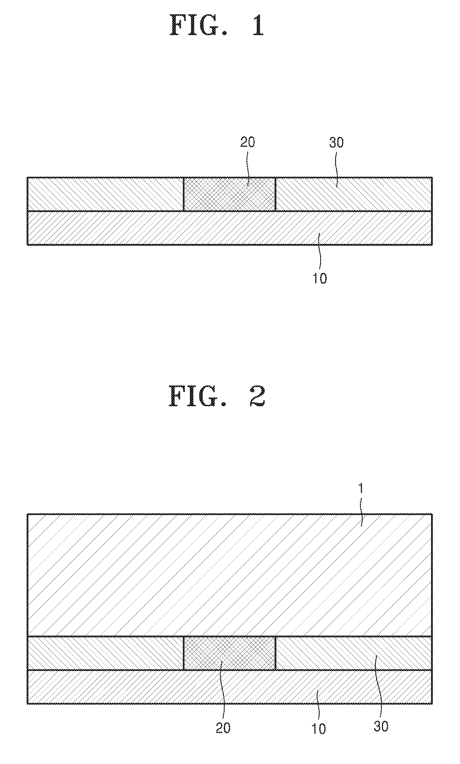
A semiconductor manufacturing method includes depositing a low-k dielectric layer, forming a trench in the low-k dielectric layer, forming a barrier layer in the trench, filling a metal on the barrier layer, planarizing the metal, and forming a capping layer on the planarized metal, wherein the capping layer includes at least two layers.
| Inventors: | Lee; Choong Man (Chungcheongnam-do, KR), Yoo; Yong Min (Seoul, KR), Kim; Young Jae (Chungcheongnam-do, KR), Chun; Seung Ju (Chungcheongnam-do, KR), Kim; Sun Ja (Chungcheongnam-do, KR) | ||||||||||
|---|---|---|---|---|---|---|---|---|---|---|---|
| Applicant: |
|
||||||||||
| Assignee: | ASM IP Holding B.V. (Almere,
NL) |
||||||||||
| Family ID: | 60330372 | ||||||||||
| Appl. No.: | 15/499,647 | ||||||||||
| Filed: | April 27, 2017 |
Prior Publication Data
| Document Identifier | Publication Date | |
|---|---|---|
| US 20170338192 A1 | Nov 23, 2017 | |
Foreign Application Priority Data
| May 17, 2016 [KR] | 10-2016-0060210 | |||
| Current U.S. Class: | 1/1 |
| Current CPC Class: | H01L 23/53238 (20130101); H01L 23/564 (20130101); H01L 21/76843 (20130101); H01L 23/5226 (20130101); H01L 21/76834 (20130101); H01L 21/0228 (20130101); H01L 21/76877 (20130101); H01L 21/02211 (20130101); H01L 21/0217 (20130101); H01L 21/7684 (20130101); H01L 23/53295 (20130101); H01L 21/76832 (20130101); H01L 21/76802 (20130101); H01L 21/02219 (20130101); H01L 21/02274 (20130101); H01L 21/02178 (20130101); H01L 21/02074 (20130101) |
| Current International Class: | H01L 21/4763 (20060101); H01L 21/768 (20060101); H01L 23/00 (20060101); H01L 21/02 (20060101); H01L 23/532 (20060101); H01L 23/522 (20060101) |
References Cited [Referenced By]
U.S. Patent Documents
| D30036 | January 1899 | Rhind |
| D31889 | November 1899 | Gill |
| D56051 | August 1920 | Cohn |
| 2059480 | November 1936 | Obermaier |
| 2161626 | June 1939 | Loughner et al. |
| 2266416 | December 1941 | Duclos |
| 2280778 | April 1942 | Anderson |
| 2410420 | November 1946 | Bennett |
| 2563931 | August 1951 | Harrison |
| 2660061 | November 1953 | Lewis |
| 2745640 | May 1956 | Cushman |
| 2990045 | September 1959 | Root |
| 3038951 | June 1962 | Mead |
| 3089507 | May 1963 | Drake et al. |
| 3094396 | June 1963 | Flugge et al. |
| 3232437 | February 1966 | Hultgren |
| 3263502 | August 1966 | Springfield Redwood |
| 3410349 | November 1968 | Troutman |
| 3588192 | June 1971 | Drutchas et al. |
| 3647387 | March 1972 | Benson |
| 3647716 | March 1972 | Koches |
| 3713899 | January 1973 | Sebestyen |
| 3718429 | February 1973 | Williamson |
| 3833492 | September 1974 | Bollyky |
| 3854443 | December 1974 | Baerg |
| 3862397 | January 1975 | Anderson et al. |
| 3867205 | February 1975 | Schley |
| 3885504 | May 1975 | Baermann |
| 3887790 | June 1975 | Ferguson |
| 3904371 | September 1975 | Neti |
| 3913058 | October 1975 | Nishio et al. |
| 3913617 | October 1975 | van Laar |
| 3947685 | March 1976 | Meinel |
| 3960559 | June 1976 | Suzuki |
| 4054071 | October 1977 | Patejak |
| 4058430 | November 1977 | Suntola et al. |
| 4093491 | June 1978 | Whelpton et al. |
| D249341 | September 1978 | Mertz |
| 4126027 | November 1978 | Smith et al. |
| 4134425 | January 1979 | Gussefeld et al. |
| 4145699 | March 1979 | Hu et al. |
| 4164959 | August 1979 | Wurzburger |
| 4176630 | December 1979 | Elmer |
| 4181330 | January 1980 | Kojima |
| 4194536 | March 1980 | Stine et al. |
| 4217463 | August 1980 | Swearingen |
| 4234449 | November 1980 | Wolson et al. |
| 4322592 | March 1982 | Martin |
| 4333735 | June 1982 | Hardy |
| 4355912 | October 1982 | Haak |
| 4389973 | June 1983 | Suntola et al. |
| 4393013 | July 1983 | McMenamin |
| 4401507 | August 1983 | Engle |
| 4414492 | November 1983 | Hanlet |
| 4436674 | March 1984 | McMenamin |
| 4444990 | April 1984 | Villar |
| 4454370 | June 1984 | Voznick |
| 4455193 | June 1984 | Jeuch et al. |
| 4466766 | August 1984 | Geren et al. |
| 4479831 | October 1984 | Sandow |
| 4499354 | February 1985 | Hill et al. |
| 4512113 | April 1985 | Budinger |
| 4527005 | July 1985 | McKelvey et al. |
| 4537001 | August 1985 | Uppstrom |
| 4548688 | October 1985 | Mathews |
| 4570328 | February 1986 | Price et al. |
| 4575636 | March 1986 | Caprari |
| 4578560 | March 1986 | Tanaka et al. |
| 4579378 | April 1986 | Snyders |
| 4579623 | April 1986 | Suzuki et al. |
| 4590326 | May 1986 | Woldy |
| 4611966 | September 1986 | Johnson |
| 4620998 | November 1986 | Lalvani |
| D288556 | March 1987 | Wallgren |
| 4653541 | March 1987 | Oehlschlaeger et al. |
| 4654226 | March 1987 | Jackson et al. |
| 4664769 | May 1987 | Cuomo et al. |
| 4681134 | July 1987 | Paris |
| 4718637 | January 1988 | Contin |
| 4721533 | January 1988 | Phillippi et al. |
| 4722298 | February 1988 | Rubin et al. |
| 4724272 | February 1988 | Raniere et al. |
| 4735259 | April 1988 | Vincent |
| 4749416 | June 1988 | Greenspan |
| 4753192 | June 1988 | Goldsmith et al. |
| 4756794 | July 1988 | Yoder |
| 4771015 | September 1988 | Kanai |
| 4780169 | October 1988 | Stark et al. |
| 4789294 | December 1988 | Sato et al. |
| 4821674 | April 1989 | deBoer et al. |
| 4827430 | May 1989 | Aid et al. |
| 4830515 | May 1989 | Cortes |
| 4837113 | June 1989 | Luttmer et al. |
| 4837185 | June 1989 | Yau et al. |
| 4854263 | August 1989 | Chang et al. |
| 4854266 | August 1989 | Simson et al. |
| 4857137 | August 1989 | Tachi et al. |
| 4857382 | August 1989 | Liu et al. |
| 4882199 | November 1989 | Sadoway et al. |
| 4916091 | April 1990 | Freeman et al. |
| 4934831 | June 1990 | Volbrecht |
| 4949848 | August 1990 | Kos |
| D311126 | October 1990 | Crowley |
| 4976996 | December 1990 | Monkowski et al. |
| 4978567 | December 1990 | Miller |
| 4984904 | January 1991 | Nakano et al. |
| 4985114 | January 1991 | Okudaira |
| 4986215 | January 1991 | Yamada |
| 4987856 | January 1991 | Hey |
| 4989992 | February 1991 | Piai |
| 4991614 | February 1991 | Hammel |
| 5013691 | May 1991 | Lory et al. |
| 5027746 | July 1991 | Frijlink |
| 5028366 | July 1991 | Harakal et al. |
| 5057436 | October 1991 | Ball |
| 5060322 | October 1991 | Delepine |
| 5061083 | October 1991 | Grimm et al. |
| 5062386 | November 1991 | Christensen |
| 5065698 | November 1991 | Koike |
| 5071258 | December 1991 | Usher et al. |
| 5074017 | December 1991 | Toya et al. |
| 5098638 | March 1992 | Sawada |
| 5098865 | March 1992 | Machado |
| 5104514 | April 1992 | Quartarone |
| 5108192 | April 1992 | Mailliet et al. |
| 5116018 | May 1992 | Friemoth et al. |
| D327534 | June 1992 | Manville |
| 5119760 | June 1992 | McMillan et al. |
| 5130003 | July 1992 | Conrad |
| 5137286 | August 1992 | Whitford |
| 5154301 | October 1992 | Kos |
| 5158128 | October 1992 | Inoue et al. |
| 5167716 | December 1992 | Boitnott et al. |
| 5176451 | January 1993 | Sasada |
| 5178682 | January 1993 | Tsukamoto et al. |
| 5181779 | January 1993 | Shia et al. |
| 5183511 | February 1993 | Yamazaki et al. |
| 5192717 | March 1993 | Kawakami |
| 5194401 | March 1993 | Adams et al. |
| 5199603 | April 1993 | Prescott |
| 5213650 | May 1993 | Wang et al. |
| 5221556 | June 1993 | Hawkins et al. |
| 5225366 | July 1993 | Yoder et al. |
| 5226383 | July 1993 | Bhat |
| 5228114 | July 1993 | Suzuki |
| 5242539 | September 1993 | Kumihashi et al. |
| 5243195 | September 1993 | Nishi |
| 5243202 | September 1993 | Mori et al. |
| 5246218 | September 1993 | Yap et al. |
| 5246500 | September 1993 | Samata et al. |
| 5259881 | November 1993 | Edwards et al. |
| 5266526 | November 1993 | Aoyama |
| 5271967 | December 1993 | Kramer et al. |
| 5278494 | January 1994 | Obigane |
| 5284519 | February 1994 | Gadgil |
| 5288684 | February 1994 | Yamazaki et al. |
| 5294778 | March 1994 | Carman et al. |
| 5306666 | April 1994 | Izumi |
| 5306946 | April 1994 | Yamamoto |
| 5310456 | May 1994 | Kadomura |
| 5314570 | May 1994 | Ikegaya et al. |
| 5315092 | May 1994 | Takahashi et al. |
| 5326427 | July 1994 | Jerbic |
| 5336327 | August 1994 | Lee |
| 5354580 | October 1994 | Goela et al. |
| 5356478 | October 1994 | Chen et al. |
| 5356672 | October 1994 | Schmitt et al. |
| 5360269 | November 1994 | Ogawa et al. |
| 5364667 | November 1994 | Rhieu |
| D353452 | December 1994 | Groenhoff |
| 5374315 | December 1994 | Deboer et al. |
| 5380367 | January 1995 | Bertone |
| 5382311 | January 1995 | Ishikawa et al. |
| 5388945 | February 1995 | Garric et al. |
| 5404082 | April 1995 | Hernandez et al. |
| 5407449 | April 1995 | Zinger |
| 5413813 | May 1995 | Cruse et al. |
| 5414221 | May 1995 | Gardner |
| 5415753 | May 1995 | Hurwitt et al. |
| 5421893 | June 1995 | Perlov |
| 5422139 | June 1995 | Fischer |
| 5423942 | June 1995 | Robbins et al. |
| 5430011 | July 1995 | Tanaka et al. |
| 5444217 | August 1995 | Moore |
| 5453124 | September 1995 | Moslehi et al. |
| 5494494 | February 1996 | Mizuno et al. |
| 5496408 | March 1996 | Motoda et al. |
| 5504042 | April 1996 | Cho et al. |
| 5514439 | May 1996 | Sibley |
| 5518549 | May 1996 | Hellwig |
| 5523616 | June 1996 | Yasuhide |
| 5527111 | June 1996 | Lysen et al. |
| 5527417 | June 1996 | Iida et al. |
| 5531835 | July 1996 | Fodor et al. |
| 5540898 | July 1996 | Davidson |
| 5558717 | September 1996 | Zhao et al. |
| 5559046 | September 1996 | Oishi et al. |
| 5574247 | November 1996 | Nishitani et al. |
| 5576629 | November 1996 | Turner |
| 5577331 | November 1996 | Suzuki |
| 5583736 | December 1996 | Anderson et al. |
| 5589002 | December 1996 | Su |
| 5589110 | December 1996 | Motoda et al. |
| 5595606 | January 1997 | Fujikawa et al. |
| 5601641 | February 1997 | Stephens |
| 5604410 | February 1997 | Vollkommer et al. |
| 5616264 | April 1997 | Nishi et al. |
| 5616947 | April 1997 | Tamura |
| 5621982 | April 1997 | Yamashita |
| 5632919 | May 1997 | MacCracken et al. |
| D380527 | July 1997 | Velez |
| 5656093 | August 1997 | Burkhart et al. |
| 5663899 | September 1997 | Zvonar et al. |
| 5665608 | September 1997 | Chapple-Sokol et al. |
| 5679215 | October 1997 | Barnes et al. |
| 5681779 | October 1997 | Pasch et al. |
| 5683517 | November 1997 | Shan |
| 5695567 | December 1997 | Kordina |
| 5697706 | December 1997 | Ciaravino et al. |
| 5700729 | December 1997 | Lee et al. |
| 5708825 | January 1998 | Sotomayor |
| 5711811 | January 1998 | Suntola et al. |
| 5716133 | February 1998 | Hosokawa et al. |
| 5718574 | February 1998 | Shimazu |
| D392855 | March 1998 | Pillow |
| 5724748 | March 1998 | Brooks |
| 5728223 | March 1998 | Murakarni et al. |
| 5730801 | March 1998 | Tepman et al. |
| 5732744 | March 1998 | Barr et al. |
| 5736314 | April 1998 | Hayes et al. |
| 5753835 | May 1998 | Gustin |
| 5761328 | June 1998 | Solberg et al. |
| 5777838 | July 1998 | Tamagawa et al. |
| 5779203 | July 1998 | Edlinger |
| 5781693 | July 1998 | Balance et al. |
| 5782979 | July 1998 | Kaneno |
| 5791782 | August 1998 | Wooten et al. |
| 5792272 | August 1998 | Van Os et al. |
| 5796074 | August 1998 | Edelstein et al. |
| 5801104 | September 1998 | Schuegraf et al. |
| 5806980 | September 1998 | Berrian |
| 5813851 | September 1998 | Nakao |
| 5819092 | October 1998 | Ferguson et al. |
| 5819434 | October 1998 | Herchen et al. |
| 5827435 | October 1998 | Seiji |
| 5827757 | October 1998 | Robinson, Jr. et al. |
| 5836483 | November 1998 | Disel |
| 5837058 | November 1998 | Chen et al. |
| 5837320 | November 1998 | Hampden-Smith et al. |
| 5844683 | December 1998 | Pavloski et al. |
| 5846332 | December 1998 | Zhao et al. |
| 5851294 | December 1998 | Young et al. |
| 5852879 | December 1998 | Schumaier |
| 5853484 | December 1998 | Jeong |
| 5855680 | January 1999 | Soininen et al. |
| 5855681 | January 1999 | Maydan et al. |
| 5857777 | January 1999 | Schuh |
| 5863123 | January 1999 | Lee |
| 5865205 | February 1999 | Wilmer |
| 5873942 | February 1999 | Park |
| 5877095 | March 1999 | Tamura et al. |
| 5879128 | March 1999 | Tietz et al. |
| 5884640 | March 1999 | Fishkin et al. |
| D409894 | May 1999 | McClurg |
| 5908672 | June 1999 | Ryu |
| 5916365 | June 1999 | Sherman |
| D412270 | July 1999 | Fredrickson |
| 5920798 | July 1999 | Higuchi et al. |
| 5937323 | August 1999 | Orczyk et al. |
| 5947718 | September 1999 | Weaver |
| 5954375 | September 1999 | Trickle et al. |
| 5961775 | October 1999 | Fujimura |
| 5968275 | October 1999 | Lee et al. |
| 5970621 | October 1999 | Bazydola |
| 5975492 | November 1999 | Brenes |
| 5979506 | November 1999 | Aarseth |
| 5982931 | November 1999 | Ishimaru |
| 5984391 | November 1999 | Vanderpot et al. |
| 5987480 | November 1999 | Donohue et al. |
| 5997588 | December 1999 | Goodwin |
| 5997768 | December 1999 | Scully |
| 5998870 | December 1999 | Lee et al. |
| 6001267 | December 1999 | Van Os et al. |
| D419652 | January 2000 | Hall et al. |
| 6013553 | January 2000 | Wallace |
| 6013920 | January 2000 | Gordon et al. |
| 6015465 | January 2000 | Kholodenko et al. |
| 6017779 | January 2000 | Miyasaka |
| 6017818 | January 2000 | Lu |
| 6024799 | February 2000 | Chen |
| 6035101 | March 2000 | Sajoto et al. |
| 6042652 | March 2000 | Hyun |
| 6044860 | April 2000 | Nue |
| 6045260 | April 2000 | Schwartz et al. |
| 6048154 | April 2000 | Wytman |
| 6050506 | April 2000 | Guo et al. |
| 6054678 | April 2000 | Miyazaki |
| 6060691 | May 2000 | Minami et al. |
| 6060721 | May 2000 | Huang |
| 6068441 | May 2000 | Raaijmakers et al. |
| 6072163 | June 2000 | Armstrong |
| 6073973 | June 2000 | Boscaljon et al. |
| 6074443 | June 2000 | Venkatesh |
| 6083321 | July 2000 | Lei et al. |
| 6086677 | July 2000 | Umotoy et al. |
| 6091062 | July 2000 | Pfahnl et al. |
| 6093252 | July 2000 | Wengert et al. |
| 6093253 | July 2000 | Lofgren |
| 6096267 | August 2000 | Kishkovich |
| 6099302 | August 2000 | Hong et al. |
| 6102565 | August 2000 | Kita et al. |
| 6104011 | August 2000 | Juliano |
| 6104401 | August 2000 | Parsons |
| 6106678 | August 2000 | Shufflebotham |
| 6119710 | September 2000 | Brown |
| 6121061 | September 2000 | Van Bilsen et al. |
| 6121158 | September 2000 | Benchikha et al. |
| 6122036 | September 2000 | Yamasaki et al. |
| 6124600 | September 2000 | Moroishi et al. |
| 6125789 | October 2000 | Gupta et al. |
| 6126848 | October 2000 | Li et al. |
| 6129044 | October 2000 | Zhao et al. |
| 6129546 | October 2000 | Sada |
| 6134807 | October 2000 | Komino |
| 6137240 | October 2000 | Bogdan et al. |
| 6140252 | October 2000 | Cho et al. |
| 6148761 | November 2000 | Majewski et al. |
| 6158941 | December 2000 | Muka et al. |
| 6160244 | December 2000 | Ohashi |
| 6161500 | December 2000 | Kopacz et al. |
| 6162323 | December 2000 | Koshimizu et al. |
| 6174809 | January 2001 | Kang et al. |
| 6178918 | January 2001 | Van Os et al. |
| 6180979 | January 2001 | Hofman et al. |
| 6187672 | February 2001 | Zhao |
| 6187691 | February 2001 | Fukuda |
| 6190634 | February 2001 | Lieber et al. |
| 6191399 | February 2001 | Van Bilsen |
| 6194037 | February 2001 | Terasaki et al. |
| 6201999 | March 2001 | Jevtic |
| 6203613 | March 2001 | Gates et al. |
| 6207932 | March 2001 | Yoo |
| 6212789 | April 2001 | Kato |
| 6214122 | April 2001 | Thompson |
| 6217658 | April 2001 | Orczyk et al. |
| 6218288 | April 2001 | Li et al. |
| 6225020 | May 2001 | Jung et al. |
| 6235858 | May 2001 | Swarup et al. |
| 6242359 | June 2001 | Misra |
| 6243654 | June 2001 | Johnson et al. |
| 6245665 | June 2001 | Yokoyama |
| 6250250 | June 2001 | Maishev et al. |
| 6257758 | July 2001 | Culbertson |
| 6264467 | July 2001 | Andreas et al. |
| 6271148 | August 2001 | Kao |
| 6274878 | August 2001 | Li et al. |
| 6281098 | August 2001 | Wang |
| 6281141 | August 2001 | Das et al. |
| 6284050 | September 2001 | Shi et al. |
| 6287965 | September 2001 | Kang et al. |
| 6293700 | September 2001 | Lund et al. |
| D449873 | October 2001 | Bronson |
| 6296909 | October 2001 | Spitsberg |
| 6299133 | October 2001 | Waragai et al. |
| 6302964 | October 2001 | Umotoy et al. |
| 6303523 | October 2001 | Cheung |
| 6305898 | October 2001 | Yamagishi et al. |
| 6311016 | October 2001 | Yanagawa et al. |
| 6312525 | November 2001 | Bright et al. |
| 6315512 | November 2001 | Tabrizi et al. |
| 6316162 | November 2001 | Jung et al. |
| D451893 | December 2001 | Robson |
| D452220 | December 2001 | Robson |
| 6325858 | December 2001 | Wengert |
| 6326597 | December 2001 | Lubomirsky et al. |
| 6329297 | December 2001 | Balish |
| 6342427 | January 2002 | Choi et al. |
| 6344084 | February 2002 | Koinuma et al. |
| 6344232 | February 2002 | Jones et al. |
| 6347636 | February 2002 | Xia |
| 6350391 | February 2002 | Livshits et al. |
| 6352945 | March 2002 | Matsuki |
| D455024 | April 2002 | Mimick et al. |
| 6367410 | April 2002 | Leahey et al. |
| 6368773 | April 2002 | Jung et al. |
| 6368987 | April 2002 | Kopacz et al. |
| 6370796 | April 2002 | Zucker |
| 6372583 | April 2002 | Tyagi |
| 6374831 | April 2002 | Chandran |
| 6375312 | April 2002 | Ikeda et al. |
| 6375750 | April 2002 | Van Os et al. |
| D457609 | May 2002 | Piano |
| 6383566 | May 2002 | Zagdoun |
| 6383955 | May 2002 | Matsuki |
| 6387207 | May 2002 | Janakiraman |
| 6391803 | May 2002 | Kim et al. |
| 6395650 | May 2002 | Callegari et al. |
| 6398184 | June 2002 | Sowada et al. |
| 6410459 | June 2002 | Blalock et al. |
| 6413321 | July 2002 | Kim et al. |
| 6413583 | July 2002 | Moghadam et al. |
| 6420279 | July 2002 | Ono et al. |
| D461233 | August 2002 | Whalen |
| D461882 | August 2002 | Piano |
| 6432849 | August 2002 | Endo et al. |
| 6435798 | August 2002 | Satoh |
| 6435865 | August 2002 | Tseng et al. |
| 6436819 | August 2002 | Zhang |
| 6437444 | August 2002 | Andideh |
| 6438502 | August 2002 | Awtrey |
| 6441350 | August 2002 | Stoddard et al. |
| 6445574 | September 2002 | Saw et al. |
| 6446573 | September 2002 | Hirayama et al. |
| 6447232 | September 2002 | Davis et al. |
| 6447651 | September 2002 | Ishikawa et al. |
| 6448192 | September 2002 | Kaushik |
| 6450757 | September 2002 | Saeki |
| 6451713 | September 2002 | Tay et al. |
| 6454860 | September 2002 | Metzner et al. |
| 6455225 | September 2002 | Kong et al. |
| 6455445 | September 2002 | Matsuki |
| 6461435 | October 2002 | Littau et al. |
| 6468924 | October 2002 | Lee |
| 6471779 | October 2002 | Nishio et al. |
| 6472266 | October 2002 | Yu et al. |
| 6475276 | November 2002 | Elers et al. |
| 6475930 | November 2002 | Junker et al. |
| 6478872 | November 2002 | Chae et al. |
| 6482331 | November 2002 | Lu et al. |
| 6482663 | November 2002 | Buckland |
| 6483989 | November 2002 | Okada et al. |
| 6494065 | December 2002 | Babbitt |
| 6494998 | December 2002 | Brcka |
| 6496819 | December 2002 | Bello et al. |
| 6499533 | December 2002 | Yamada |
| 6503079 | January 2003 | Kogano et al. |
| 6503562 | January 2003 | Saito et al. |
| 6503826 | January 2003 | Oda |
| 6506253 | January 2003 | Sakuma |
| 6507410 | January 2003 | Robertson et al. |
| 6511539 | January 2003 | Raaijmakers |
| 6514313 | February 2003 | Spiegelman |
| 6514666 | February 2003 | Choi et al. |
| 6521295 | February 2003 | Remington |
| 6521547 | February 2003 | Chang et al. |
| 6528430 | March 2003 | Kwan |
| 6528767 | March 2003 | Bagley et al. |
| 6531193 | March 2003 | Fonash et al. |
| 6531412 | March 2003 | Conti et al. |
| 6534133 | March 2003 | Kaloyeros et al. |
| 6534395 | March 2003 | Werkhoven et al. |
| 6536950 | March 2003 | Green |
| 6544906 | April 2003 | Rotondaro et al. |
| 6552209 | April 2003 | Lei et al. |
| 6558755 | May 2003 | Berry et al. |
| 6559026 | May 2003 | Rossman et al. |
| 6566278 | May 2003 | Harvey et al. |
| 6569239 | May 2003 | Arai et al. |
| 6569971 | May 2003 | Roh et al. |
| 6573030 | June 2003 | Fairbairn et al. |
| 6574644 | June 2003 | Hsu et al. |
| 6576062 | June 2003 | Matsuse |
| 6576064 | June 2003 | Griffiths et al. |
| 6576300 | June 2003 | Berry et al. |
| 6576564 | June 2003 | Agarwal |
| 6578589 | June 2003 | Mayusumi |
| 6579833 | June 2003 | McNallan et al. |
| 6580050 | June 2003 | Miller et al. |
| 6583048 | June 2003 | Vincent et al. |
| 6589707 | July 2003 | Lee et al. |
| 6589868 | July 2003 | Rossman |
| 6590251 | July 2003 | Kang et al. |
| 6594550 | July 2003 | Okrah |
| 6596653 | July 2003 | Tan |
| 6598559 | July 2003 | Vellore et al. |
| 6607868 | August 2003 | Choi |
| 6607948 | August 2003 | Sugiyama et al. |
| 6608745 | August 2003 | Tsuruta et al. |
| 6620251 | September 2003 | Kitano |
| 6624064 | September 2003 | Sahin |
| 6627268 | September 2003 | Fair et al. |
| 6627503 | September 2003 | Ma et al. |
| 6632478 | October 2003 | Gaillard et al. |
| 6633364 | October 2003 | Hayashi |
| 6635117 | October 2003 | Kinnard et al. |
| 6638839 | October 2003 | Deng et al. |
| 6645304 | November 2003 | Yamaguchi |
| 6648974 | November 2003 | Ogliari et al. |
| 6649921 | November 2003 | Cekic et al. |
| 6652924 | November 2003 | Sherman |
| 6656281 | December 2003 | Ueda |
| 6660662 | December 2003 | Ishikawa et al. |
| 6662817 | December 2003 | Yamagishi |
| 6673196 | January 2004 | Oyabu |
| 6676290 | January 2004 | Lu |
| 6682971 | January 2004 | Tsuneda et al. |
| 6682973 | January 2004 | Paton et al. |
| D486891 | February 2004 | Cronce |
| 6684659 | February 2004 | Tanaka et al. |
| 6688784 | February 2004 | Templeton |
| 6689220 | February 2004 | Nguyen |
| 6692575 | February 2004 | Omstead et al. |
| 6692576 | February 2004 | Halpin et al. |
| 6699003 | March 2004 | Saeki |
| 6699399 | March 2004 | Qian et al. |
| 6709989 | March 2004 | Ramdani et al. |
| 6710364 | March 2004 | Guldi et al. |
| 6710857 | March 2004 | Kondo |
| 6713824 | March 2004 | Mikata |
| 6716571 | April 2004 | Gabriel |
| 6720260 | April 2004 | Fair et al. |
| 6722837 | April 2004 | Inui |
| 6723642 | April 2004 | Lim et al. |
| 6730614 | May 2004 | Lim et al. |
| 6732006 | May 2004 | Haanstra et al. |
| 6734090 | May 2004 | Agarwala et al. |
| 6740853 | May 2004 | Johnson et al. |
| 6743475 | June 2004 | Skarp et al. |
| 6743738 | June 2004 | Todd et al. |
| 6745095 | June 2004 | Ben-Dov |
| 6753507 | June 2004 | Fure et al. |
| 6755221 | June 2004 | Jeong et al. |
| 6756085 | June 2004 | Waldfried |
| 6756293 | June 2004 | Li et al. |
| 6756318 | June 2004 | Nguyen et al. |
| 6759098 | July 2004 | Han |
| 6760981 | July 2004 | Leap |
| 6784108 | August 2004 | Donohoe et al. |
| D497977 | November 2004 | Engelbrektsson |
| 6811960 | November 2004 | Lee et al. |
| 6815350 | November 2004 | Kim et al. |
| 6820570 | November 2004 | Kilpela et al. |
| 6821910 | November 2004 | Adomaitis et al. |
| 6824665 | November 2004 | Shelnut et al. |
| 6825134 | November 2004 | Law et al. |
| 6828235 | December 2004 | Takano |
| 6831004 | December 2004 | Byun |
| 6835039 | December 2004 | Van Den Berg |
| 6846146 | January 2005 | Inui |
| 6846515 | January 2005 | Vrtis |
| 6846742 | January 2005 | Rossman |
| 6847014 | January 2005 | Benjamin et al. |
| 6858524 | February 2005 | Haukka et al. |
| 6858547 | February 2005 | Metzner |
| 6863019 | March 2005 | Shamouilian |
| 6863281 | March 2005 | Endou et al. |
| 6864041 | March 2005 | Brown |
| 6872258 | March 2005 | Park et al. |
| 6872259 | March 2005 | Strang |
| 6874247 | April 2005 | Hsu |
| 6874480 | April 2005 | Ismailov |
| 6875677 | April 2005 | Conley, Jr. et al. |
| 6876017 | April 2005 | Goodner |
| 6878402 | April 2005 | Chiang et al. |
| 6884066 | April 2005 | Nguyen et al. |
| 6884295 | April 2005 | Ishii |
| 6884319 | April 2005 | Kim |
| D505590 | May 2005 | Greiner |
| 6889211 | May 2005 | Yoshiura et al. |
| 6889864 | May 2005 | Lindfors et al. |
| 6895158 | May 2005 | Alyward et al. |
| 6899507 | May 2005 | Yamagishi et al. |
| 6909839 | June 2005 | Wang et al. |
| 6911092 | June 2005 | Sneh |
| 6913152 | July 2005 | Zuk |
| 6913796 | July 2005 | Albano et al. |
| 6917755 | July 2005 | Nguyen et al. |
| 6924078 | August 2005 | Lee et al. |
| 6929700 | August 2005 | Tan et al. |
| 6930041 | August 2005 | Agarwal |
| 6930059 | August 2005 | Conley, Jr. et al. |
| 6935269 | August 2005 | Lee et al. |
| 6939817 | September 2005 | Sandhu et al. |
| 6942753 | September 2005 | Choi et al. |
| 6951587 | October 2005 | Narushima |
| 6953609 | October 2005 | Carollo |
| 6955836 | October 2005 | Kumagai et al. |
| 6972055 | December 2005 | Sferlazzo |
| 6972478 | December 2005 | Waite et al. |
| 6974781 | December 2005 | Timmermans et al. |
| 6975921 | December 2005 | Verhaar |
| 6976822 | December 2005 | Woodruff |
| 6981832 | January 2006 | Zinger et al. |
| 6982046 | January 2006 | Srivastava et al. |
| 6984595 | January 2006 | Yamazaki |
| 6985788 | January 2006 | Haanstra et al. |
| 6987155 | January 2006 | Roh et al. |
| 6990430 | January 2006 | Hosek |
| 7005227 | February 2006 | Yueh et al. |
| 7005391 | February 2006 | Min |
| 7010580 | March 2006 | Fu et al. |
| 7017514 | March 2006 | Shepherd et al. |
| 7018941 | March 2006 | Cui et al. |
| 7021881 | April 2006 | Yamagishi |
| 7036453 | May 2006 | Ishikawa et al. |
| 7041609 | May 2006 | Vaartstra |
| 7045430 | May 2006 | Ahn et al. |
| 7049247 | May 2006 | Gates et al. |
| 7053009 | May 2006 | Conley, Jr. et al. |
| 7055875 | June 2006 | Bonora |
| 7062161 | June 2006 | Kusuda et al. |
| 7070178 | July 2006 | Van Der Toorn et al. |
| 7071051 | July 2006 | Jeon et al. |
| 7073834 | July 2006 | Matsumoto et al. |
| 7080545 | July 2006 | Dimeo et al. |
| 7084060 | August 2006 | Furukawa |
| 7084079 | August 2006 | Conti et al. |
| 7085623 | August 2006 | Siegers |
| 7088003 | August 2006 | Gates et al. |
| 7090394 | August 2006 | Hashikura et al. |
| 7092287 | August 2006 | Beulens et al. |
| 7098149 | August 2006 | Lukas |
| 7101763 | September 2006 | Anderson et al. |
| 7109098 | September 2006 | Ramaswamy et al. |
| 7109114 | September 2006 | Chen et al. |
| 7111232 | September 2006 | Bascom |
| 7115838 | October 2006 | Kurara et al. |
| 7122085 | October 2006 | Shero et al. |
| 7122222 | October 2006 | Xiao et al. |
| 7129165 | October 2006 | Basol et al. |
| 7132360 | November 2006 | Schaeffer et al. |
| 7135421 | November 2006 | Ahn et al. |
| 7143897 | December 2006 | Guzman et al. |
| 7147766 | December 2006 | Uzoh et al. |
| 7153542 | December 2006 | Nguyen et al. |
| 7156380 | January 2007 | Soininen |
| 7163393 | January 2007 | Adachi et al. |
| 7163721 | January 2007 | Zhang et al. |
| 7163900 | January 2007 | Weber |
| 7168852 | January 2007 | Linnarsson |
| 7172497 | February 2007 | Basol et al. |
| 7186648 | March 2007 | Rozbicki |
| 7192824 | March 2007 | Ahn et al. |
| 7192892 | March 2007 | Ahn et al. |
| 7195693 | March 2007 | Cowans |
| 7201943 | April 2007 | Park et al. |
| 7204887 | April 2007 | Kawamura et al. |
| 7205246 | April 2007 | MacNeil et al. |
| 7205247 | April 2007 | Lee et al. |
| 7207763 | April 2007 | Lee |
| 7208389 | April 2007 | Tipton et al. |
| 7210925 | May 2007 | Adachi |
| 7211524 | May 2007 | Ryu et al. |
| 7211525 | May 2007 | Shanker |
| 7214630 | May 2007 | Varadarajan et al. |
| 7223014 | May 2007 | Lojen |
| 7208413 | June 2007 | Byun et al. |
| 7234476 | June 2007 | Arai |
| 7235137 | June 2007 | Kitayama et al. |
| 7235482 | June 2007 | Wu |
| 7235501 | June 2007 | Ahn et al. |
| 7238596 | July 2007 | Kouvetakis et al. |
| 7238616 | July 2007 | Agarwal |
| 7238653 | July 2007 | Lee et al. |
| 7265061 | September 2007 | Cho et al. |
| 7274867 | September 2007 | Peukert |
| D553104 | October 2007 | Oohashi et al. |
| 7279256 | October 2007 | Son |
| 7290813 | November 2007 | Bonora |
| 7294581 | November 2007 | Haverkort et al. |
| 7296460 | November 2007 | Dimeo et al. |
| 7297641 | November 2007 | Todd et al. |
| 7298009 | November 2007 | Yan et al. |
| D557226 | December 2007 | Uchino et al. |
| 7307028 | December 2007 | Goto et al. |
| 7307178 | December 2007 | Kiyomori et al. |
| 7312148 | December 2007 | Ramaswamy et al. |
| 7312162 | December 2007 | Ramaswamy et al. |
| 7312494 | December 2007 | Ahn et al. |
| 7320544 | January 2008 | Hsieh |
| 7323401 | January 2008 | Ramaswamy et al. |
| 7326657 | February 2008 | Xia et al. |
| 7327948 | February 2008 | Shrinivasan |
| 7329947 | February 2008 | Adachi et al. |
| 7335611 | February 2008 | Ramaswamy et al. |
| 7351057 | April 2008 | Berenbak et al. |
| 7354847 | April 2008 | Chan et al. |
| 7354873 | April 2008 | Fukazawa et al. |
| 7356762 | April 2008 | van Driel |
| 7357138 | April 2008 | Ji et al. |
| 7361447 | April 2008 | Jung |
| 7376520 | May 2008 | Wong |
| 7379785 | May 2008 | Higashi et al. |
| 7381644 | June 2008 | Soubramonium et al. |
| 7387685 | June 2008 | Choi et al. |
| 7393207 | July 2008 | Imai |
| 7393418 | July 2008 | Yokogawa |
| 7393736 | July 2008 | Ahn et al. |
| 7393765 | July 2008 | Hanawa et al. |
| 7396491 | July 2008 | Marking et al. |
| 7399388 | July 2008 | Moghadam et al. |
| 7399570 | July 2008 | Lee et al. |
| 7402534 | July 2008 | Mahajani |
| 7405166 | July 2008 | Liang et al. |
| 7405454 | July 2008 | Ahn et al. |
| D575713 | August 2008 | Ratcliffe |
| 7410290 | August 2008 | Tanaka |
| 7410666 | August 2008 | Elers |
| 7411352 | August 2008 | Madocks |
| 7414281 | August 2008 | Fastow |
| D576001 | September 2008 | Brunderman |
| 7422635 | September 2008 | Zheng et al. |
| 7422653 | September 2008 | Blahnik et al. |
| 7422775 | September 2008 | Ramaswamy et al. |
| 7429532 | September 2008 | Ramaswamy et al. |
| 7431966 | October 2008 | Derderian et al. |
| 7432476 | October 2008 | Morita et al. |
| 7437060 | October 2008 | Wang et al. |
| 7442275 | October 2008 | Cowans |
| 7467632 | December 2008 | Lee et al. |
| 7475588 | January 2009 | Dimeo et al. |
| 7476291 | January 2009 | Wang et al. |
| 7479198 | January 2009 | Guffrey |
| 7482247 | January 2009 | Papasouliotis |
| 7482283 | January 2009 | Yamasaki et al. |
| D585968 | February 2009 | Elkins et al. |
| 7489389 | February 2009 | Shibazaki et al. |
| 7494882 | February 2009 | Vitale |
| 7497614 | March 2009 | Gaff |
| 7498242 | March 2009 | Kumar et al. |
| 7501292 | March 2009 | Matsushita et al. |
| 7501355 | March 2009 | Bhatia et al. |
| 7503980 | March 2009 | Kida et al. |
| D590933 | April 2009 | Vansell |
| 7514375 | April 2009 | Shanker et al. |
| D593969 | June 2009 | Li |
| 7541297 | June 2009 | Mallick et al. |
| 7547363 | June 2009 | Tomiyasu et al. |
| 7547633 | June 2009 | Ranish et al. |
| 7550396 | June 2009 | Frohberg et al. |
| 7561982 | July 2009 | Rund et al. |
| 7563715 | July 2009 | Haukka et al. |
| 7566891 | July 2009 | Rocha-Alvarez et al. |
| 7575968 | August 2009 | Sadaka et al. |
| 7579285 | August 2009 | Zimmerman et al. |
| 7579785 | August 2009 | Shinmen et al. |
| D600223 | September 2009 | Aggarwal |
| 7582555 | September 2009 | Lang |
| 7582575 | September 2009 | Fukazawa et al. |
| 7589003 | September 2009 | Kouvetakis et al. |
| 7589029 | September 2009 | Derderian et al. |
| 7591601 | September 2009 | Matsuoka et al. |
| D602575 | October 2009 | Breda |
| 7598513 | October 2009 | Kouvetakis et al. |
| 7601223 | October 2009 | Lindfors et al. |
| 7601225 | October 2009 | Tuominen et al. |
| 7601652 | October 2009 | Singh et al. |
| 7611751 | November 2009 | Elers |
| 7611980 | November 2009 | Wells et al. |
| 7618226 | November 2009 | Takizawa |
| 7621672 | November 2009 | Ripley |
| 7622369 | November 2009 | Lee et al. |
| 7622378 | November 2009 | Liu et al. |
| 7623940 | November 2009 | Huskamp et al. |
| D606952 | December 2009 | Lee |
| 7625820 | December 2009 | Papasouliotis |
| 7629277 | December 2009 | Ghatnagar |
| 7632549 | December 2009 | Goundar |
| 7640142 | December 2009 | Tachikawa et al. |
| 7645341 | January 2010 | Kennedy et al. |
| 7645484 | January 2010 | Ishizaka |
| 7648927 | January 2010 | Singh et al. |
| 7651269 | January 2010 | Comendant |
| 7651583 | January 2010 | Kent et al. |
| 7651955 | January 2010 | Ravish et al. |
| 7651959 | January 2010 | Fukazawa et al. |
| 7651961 | January 2010 | Clark |
| D609652 | February 2010 | Nagasaka |
| D609655 | February 2010 | Sugimoto |
| 7661299 | February 2010 | Kusunoki |
| 7678197 | March 2010 | Maki |
| 7678715 | March 2010 | Mungekar et al. |
| 7682454 | March 2010 | Sneh |
| 7682657 | March 2010 | Sherman |
| D613829 | April 2010 | Griffin et al. |
| D614153 | April 2010 | Fondurulia et al. |
| D614267 | April 2010 | Breda |
| D614268 | April 2010 | Breda |
| D614593 | April 2010 | Lee |
| 7690881 | April 2010 | Yamagishi |
| 7691205 | April 2010 | Ikedo |
| 7692171 | April 2010 | Kaszuba et al. |
| 7695808 | April 2010 | Tuma |
| 7713874 | May 2010 | Milligan |
| 7716993 | May 2010 | Ozawa et al. |
| 7720560 | May 2010 | Menser et al. |
| 7723648 | May 2010 | Tsukamoto et al. |
| 7727864 | June 2010 | Elers |
| 7732343 | June 2010 | Niroomand et al. |
| 7736437 | June 2010 | Cadwell et al. |
| 7736528 | June 2010 | Okita et al. |
| 7740705 | June 2010 | Li |
| 7745346 | June 2010 | Hausmann et al. |
| 7748760 | July 2010 | Kushida |
| 7749563 | July 2010 | Zheng et al. |
| 7753584 | July 2010 | Gambino et al. |
| 7754621 | July 2010 | Putjkonen |
| 7763869 | July 2010 | Matsushita et al. |
| 7767262 | August 2010 | Clark |
| 7771796 | August 2010 | Kohno et al. |
| 7780440 | August 2010 | Shibagaki et al. |
| 7781352 | August 2010 | Fukazawa et al. |
| 7789559 | September 2010 | Waser et al. |
| 7789965 | September 2010 | Matsushita et al. |
| 7790633 | September 2010 | Tarafdar et al. |
| 7798096 | September 2010 | Mahajani et al. |
| 7803722 | September 2010 | Liang |
| 7806587 | October 2010 | Kobayashi |
| 7807566 | October 2010 | Tsuji et al. |
| 7807578 | October 2010 | Bencher et al. |
| 7816278 | October 2010 | Reed et al. |
| 7824492 | November 2010 | Tois et al. |
| 7825040 | November 2010 | Fukazawa et al. |
| 7829460 | November 2010 | Streck et al. |
| 7833353 | November 2010 | Furukawahara et al. |
| 7838084 | November 2010 | Derderian et al. |
| 7842518 | November 2010 | Miyajima |
| 7842622 | November 2010 | Lee et al. |
| D629874 | December 2010 | Hermans |
| 7850449 | December 2010 | Yang et al. |
| 7851019 | December 2010 | Tuominen et al. |
| 7851232 | December 2010 | van Schravendijk et al. |
| 7858519 | December 2010 | Liu et al. |
| 7858533 | December 2010 | Liu et al. |
| 7865070 | January 2011 | Nakamura |
| 7871198 | January 2011 | Rempe et al. |
| 7874726 | January 2011 | Jacobs et al. |
| 7884918 | February 2011 | Hattori |
| 7888233 | February 2011 | Gauri |
| D634329 | March 2011 | Wastrom |
| D634719 | March 2011 | Yasuda et al. |
| 7897215 | March 2011 | Fair et al. |
| 7902582 | March 2011 | Forbes et al. |
| 7906174 | March 2011 | Wu et al. |
| 7910288 | March 2011 | Abatchev et al. |
| 7915139 | March 2011 | Lang |
| 7915667 | March 2011 | Knoefler et al. |
| 7919416 | April 2011 | Lee et al. |
| 7925378 | April 2011 | Gilchrist et al. |
| 7935940 | May 2011 | Smargiassi |
| 7939447 | May 2011 | Bauer et al. |
| 7942969 | May 2011 | Riker et al. |
| 7946762 | May 2011 | Yednak |
| 7951262 | May 2011 | Koshiishi et al. |
| 7955516 | June 2011 | Chandrachood |
| 7955650 | June 2011 | Tsuji |
| 7957708 | June 2011 | Karschnia et al. |
| 7963736 | June 2011 | Takizawa et al. |
| 7967913 | June 2011 | Hua et al. |
| 7972980 | July 2011 | Lee et al. |
| 7977256 | July 2011 | Liu et al. |
| 7981751 | July 2011 | Zhu et al. |
| D643055 | August 2011 | Takahashi |
| 7989736 | August 2011 | Park et al. |
| 7992318 | August 2011 | Kawaji |
| 7994721 | August 2011 | Espiau et al. |
| 7997795 | August 2011 | Schwagerman et al. |
| 7998875 | August 2011 | Deyoung |
| 8003174 | August 2011 | Fukazawa |
| 8003919 | August 2011 | Goto et al. |
| 8004198 | August 2011 | Bakre et al. |
| 8020315 | September 2011 | Nishimura |
| 8030129 | October 2011 | Jeong |
| 8033771 | October 2011 | Gage et al. |
| 8038835 | October 2011 | Hayashi et al. |
| 8041197 | October 2011 | Kasai et al. |
| 8041450 | October 2011 | Takizawa et al. |
| 8043972 | October 2011 | Liu et al. |
| 8046193 | October 2011 | Yetter et al. |
| 8048783 | November 2011 | Chung et al. |
| 8055378 | November 2011 | Numakura |
| 8060252 | November 2011 | Gage et al. |
| 8083853 | November 2011 | Choi et al. |
| D651291 | December 2011 | Liebson et al. |
| 8071451 | December 2011 | Berry |
| 8071452 | December 2011 | Raisanen |
| 8072578 | December 2011 | Yasuda et al. |
| 8076230 | December 2011 | Wei |
| 8076237 | December 2011 | Uzoh |
| 8076250 | December 2011 | Rajagopalan |
| 8076251 | December 2011 | Akae et al. |
| 8078310 | December 2011 | Nishimoto et al. |
| 8082946 | December 2011 | Laverdiere et al. |
| 8084104 | December 2011 | Shinriki et al. |
| 8084372 | December 2011 | You et al. |
| D652896 | January 2012 | Gether |
| 8092604 | January 2012 | Tomiyasu et al. |
| 8100583 | January 2012 | Aggarwal |
| D653734 | February 2012 | Sisk |
| D654884 | February 2012 | Honma |
| D655055 | February 2012 | Toll |
| 8110099 | February 2012 | Hersey et al. |
| 8114734 | February 2012 | Yang et al. |
| 8119466 | February 2012 | Avouris |
| 8129290 | March 2012 | Balseanu et al. |
| 8137462 | March 2012 | Fondurulia et al. |
| 8137465 | March 2012 | Shrinivasan et al. |
| 8138104 | March 2012 | Balseanu et al. |
| 8138676 | March 2012 | Mills |
| 8142862 | March 2012 | Lee et al. |
| 8143174 | March 2012 | Xia et al. |
| 8147242 | April 2012 | Shibagaki et al. |
| 8158512 | April 2012 | Ji et al. |
| 8172947 | May 2012 | Shibata et al. |
| 8173554 | May 2012 | Lee et al. |
| 8178436 | May 2012 | King |
| 8187679 | May 2012 | Dickey et al. |
| 8187951 | May 2012 | Wang |
| 8192901 | June 2012 | Kageyama |
| 8196234 | June 2012 | Glunk |
| 8197915 | June 2012 | Oka et al. |
| 8216380 | July 2012 | White et al. |
| 8231799 | July 2012 | Bera et al. |
| D665055 | August 2012 | Yanagisawa et al. |
| 8241991 | August 2012 | Hsieh et al. |
| 8242028 | August 2012 | van Schravendijk |
| 8242031 | August 2012 | Mallick et al. |
| 8246900 | August 2012 | Kasai et al. |
| 8252114 | August 2012 | Vukovic |
| 8252659 | August 2012 | Huyghabaert et al. |
| 8252691 | August 2012 | Beynet et al. |
| 8267633 | September 2012 | Obikane |
| 8272516 | September 2012 | Salvador |
| 8278176 | October 2012 | Bauer et al. |
| 8282769 | October 2012 | Iizuka |
| 8282847 | October 2012 | Romano |
| 8287648 | October 2012 | Reed et al. |
| 8293016 | October 2012 | Bahng et al. |
| 8293642 | October 2012 | Kim |
| 8298951 | October 2012 | Nakano |
| 8307472 | November 2012 | Saxon et al. |
| 8309173 | November 2012 | Tuominen et al. |
| 8323413 | December 2012 | Son |
| 8328939 | December 2012 | Choi et al. |
| 8329599 | December 2012 | Fukazawa et al. |
| 8334219 | December 2012 | Lee et al. |
| 8349083 | January 2013 | Takasuka et al. |
| D676943 | February 2013 | Kluss |
| 8367528 | February 2013 | Bauer et al. |
| 8372204 | February 2013 | Nakamura |
| 8378464 | February 2013 | Kato et al. |
| 8393091 | March 2013 | Kawamoto |
| 8394466 | March 2013 | Hong et al. |
| 8398773 | March 2013 | Jdira et al. |
| 8404499 | March 2013 | Moffatt |
| 8415258 | April 2013 | Akae |
| 8415259 | April 2013 | Lee et al. |
| 8440259 | May 2013 | Chiang et al. |
| 8444120 | May 2013 | Gregg et al. |
| 8445075 | May 2013 | Xu et al. |
| 8450191 | May 2013 | Wang |
| 8465811 | June 2013 | Ueda |
| 8466411 | June 2013 | Arai |
| 8470187 | June 2013 | Ha |
| 8484846 | July 2013 | Dhindsa |
| 8492170 | July 2013 | Xie et al. |
| 8496377 | July 2013 | Harr et al. |
| 8496756 | July 2013 | Cruse et al. |
| 8497213 | July 2013 | Yasui et al. |
| 8501599 | August 2013 | Ueno et al. |
| 8506162 | August 2013 | Schick et al. |
| 8506713 | August 2013 | Takagi |
| 8529701 | September 2013 | Morita |
| 8535767 | September 2013 | Kimura |
| D691974 | October 2013 | Osada et al. |
| 8551892 | October 2013 | Nakano |
| 8563443 | October 2013 | Fukazawa |
| 8569184 | October 2013 | Oka |
| 8586484 | November 2013 | Matsuyama et al. |
| 8591659 | November 2013 | Fang et al. |
| 8592005 | November 2013 | Ueda |
| D695240 | December 2013 | Iida et al. |
| 8608885 | December 2013 | Goto et al. |
| 8614047 | December 2013 | Ayothi et al. |
| 8616765 | December 2013 | Darabnia et al. |
| 8617411 | December 2013 | Singh |
| 8633115 | January 2014 | Chang et al. |
| D698904 | February 2014 | Milligan et al. |
| 8642488 | February 2014 | Liu et al. |
| 8647722 | February 2014 | Kobayashi et al. |
| 8664627 | March 2014 | Ishikawa et al. |
| 8667654 | March 2014 | Gros-Jean |
| 8668957 | March 2014 | Dussarrat et al. |
| 8669185 | March 2014 | Onizawa |
| 8679958 | March 2014 | Takamure et al. |
| D702188 | April 2014 | Jacobs |
| 8683943 | April 2014 | Onodera et al. |
| 8710580 | April 2014 | Sakuma et al. |
| 8711338 | April 2014 | Liu et al. |
| D705745 | May 2014 | Kurs et al. |
| D705762 | May 2014 | Yu |
| 8664127 | May 2014 | Bhatia et al. |
| 8720965 | May 2014 | Hino et al. |
| 8721791 | May 2014 | Choi et al. |
| 8722510 | May 2014 | Watanabe et al. |
| 8722546 | May 2014 | Fukazawa et al. |
| 8726837 | May 2014 | Patalay et al. |
| 8728832 | May 2014 | Raisanen et al. |
| 8742668 | June 2014 | Nakano et al. |
| 8759223 | June 2014 | Sapre et al. |
| 8764085 | July 2014 | Urabe |
| 8779502 | July 2014 | Sakuma et al. |
| 8784950 | July 2014 | Fukazawa et al. |
| 8784951 | July 2014 | Fukazawa et al. |
| 8785215 | July 2014 | Kobayashi et al. |
| 8785311 | July 2014 | Miyoshi |
| 8790743 | July 2014 | Omari |
| 8790749 | July 2014 | Omori et al. |
| 8802201 | August 2014 | Raisanen et al. |
| 8820809 | September 2014 | Ando et al. |
| 8821640 | September 2014 | Cleary et al. |
| 8841182 | September 2014 | Chen et al. |
| 8845806 | September 2014 | Aida et al. |
| 8846502 | September 2014 | Haukka et al. |
| D715410 | October 2014 | Lohmann |
| 8864202 | October 2014 | Schrameyer |
| D716742 | November 2014 | Jang et al. |
| 8877655 | November 2014 | Shero et al. |
| 8882923 | November 2014 | Saido et al. |
| 8883270 | November 2014 | Shero et al. |
| 8901016 | December 2014 | Jeongseok et al. |
| 8911553 | December 2014 | Baluja et al. |
| 8911826 | December 2014 | Adachi et al. |
| 8912101 | December 2014 | Tsuji et al. |
| D720838 | January 2015 | Yamagishi et al. |
| 8927906 | January 2015 | Tadokoro et al. |
| 8933375 | January 2015 | Dunn et al. |
| 8940646 | January 2015 | Chandrasekharan |
| D723153 | February 2015 | Borkholder |
| 8945305 | February 2015 | Marsh |
| 8945306 | February 2015 | Tsuda |
| 8945339 | February 2015 | Kakimoto |
| 8946830 | February 2015 | Jung et al. |
| 8956971 | February 2015 | Huakka |
| 8956983 | February 2015 | Swaminathan |
| D723330 | March 2015 | York |
| D724553 | March 2015 | Choi |
| D724701 | March 2015 | Yamagishi et al. |
| D725168 | March 2015 | Yamagishi |
| 8967608 | March 2015 | Mitsumori et al. |
| 8974868 | March 2015 | Ishikawa et al. |
| 8986456 | March 2015 | Fondurulia et al. |
| 8991214 | March 2015 | Hoshino et al. |
| 8991887 | March 2015 | Shin et al. |
| 8993054 | March 2015 | Jung et al. |
| 8993457 | March 2015 | Ramkumar et al. |
| D726365 | April 2015 | Weigensberg |
| D726884 | April 2015 | Yamagishi et al. |
| 8999102 | April 2015 | Miyoshi et al. |
| 9005539 | April 2015 | Halpin et al. |
| 9017481 | April 2015 | Pettinger et al. |
| 9017933 | April 2015 | Liu et al. |
| 9018093 | April 2015 | Tsuji et al. |
| 9018111 | April 2015 | Milligan et al. |
| 9018567 | April 2015 | de Ridder et al. |
| 9021985 | May 2015 | Alokozai et al. |
| 9023737 | May 2015 | Beynet et al. |
| 9023738 | May 2015 | Kato et al. |
| 9029253 | May 2015 | Milligan et al. |
| 9029272 | May 2015 | Nakano |
| D732145 | June 2015 | Yamagishi |
| D732644 | June 2015 | Yamagishi et al. |
| D733261 | June 2015 | Yamagishi et al. |
| D733262 | July 2015 | Yamagishi et al. |
| D733843 | July 2015 | Yamagishi |
| D734377 | July 2015 | Hirakida |
| D735836 | August 2015 | Yamagishi et al. |
| 9096931 | August 2015 | Yednak et al. |
| 9099505 | August 2015 | Kusakabe et al. |
| 9117657 | August 2015 | Nakano et al. |
| 9117866 | August 2015 | Marquardt et al. |
| D739222 | September 2015 | Chadbourne |
| 9123510 | September 2015 | Nakano et al. |
| 9123577 | September 2015 | Fujimoto et al. |
| 9129897 | September 2015 | Pore et al. |
| 9136108 | September 2015 | Matsushita et al. |
| 9136180 | September 2015 | MacHkaoutsan |
| 9142393 | September 2015 | Okabe et al. |
| 9142437 | September 2015 | Fosnight et al. |
| 9153441 | October 2015 | Takamure et al. |
| 9166012 | October 2015 | Sim et al. |
| 9169975 | October 2015 | Sarin et al. |
| 9171714 | October 2015 | Mori |
| 9171716 | October 2015 | Fukuda |
| D742202 | November 2015 | Cyphers et al. |
| D743357 | November 2015 | Vyne |
| D743513 | November 2015 | Yamagishi |
| 9177784 | November 2015 | Raisanen et al. |
| 9184047 | November 2015 | Liu et al. |
| 9190263 | November 2015 | Ishikawa et al. |
| 9190264 | November 2015 | Yuasa et al. |
| 9196483 | November 2015 | Lee et al. |
| 9202727 | December 2015 | Dunn et al. |
| 9214333 | December 2015 | Sims et al. |
| 9228259 | January 2016 | Haukka et al. |
| 9240412 | January 2016 | Xie et al. |
| 9245742 | January 2016 | Haukka |
| 9252024 | February 2016 | Lam et al. |
| 9257274 | February 2016 | Kang et al. |
| 9267850 | February 2016 | Aggarwal |
| 9281277 | March 2016 | Baek et al. |
| 9284642 | March 2016 | Nakano |
| 9297705 | March 2016 | Aggarwal |
| 9299557 | March 2016 | Tolle et al. |
| 9299595 | March 2016 | Dunn et al. |
| D753269 | April 2016 | Yamagishi et al. |
| D753629 | April 2016 | Plattard |
| 9305836 | April 2016 | Gates et al. |
| 9312155 | April 2016 | Mori |
| 9315897 | April 2016 | Byun |
| 9324811 | April 2016 | Weeks |
| 9324846 | April 2016 | Camillo |
| 9341296 | May 2016 | Yednak |
| 9343297 | May 2016 | Fukazawa et al. |
| 9343308 | May 2016 | Isii |
| 9343343 | May 2016 | Mori |
| 9343350 | May 2016 | Arai |
| 9349620 | May 2016 | Kamata et al. |
| 9353441 | May 2016 | Chung |
| 9365924 | June 2016 | Nonaka |
| 9368352 | June 2016 | Takamure et al. |
| 9370863 | June 2016 | Tsuji et al. |
| 9384987 | July 2016 | Jung et al. |
| 9390909 | July 2016 | Pasquale et al. |
| 9394608 | July 2016 | Shero et al. |
| 9396934 | July 2016 | Tolle |
| 9396956 | July 2016 | Fukazawa |
| 9404587 | August 2016 | Shugrue |
| 9412564 | August 2016 | Milligan |
| 9412582 | August 2016 | Sasaki et al. |
| 9443725 | September 2016 | Liu et al. |
| 9447498 | September 2016 | Shiba et al. |
| 9449793 | September 2016 | Shaji et al. |
| 9455138 | September 2016 | Fukazawa |
| 9464352 | October 2016 | Nakano et al. |
| 9478414 | October 2016 | Kobayashi et al. |
| 9478415 | October 2016 | Kimura |
| D770993 | November 2016 | Yoshida et al. |
| 9484191 | November 2016 | Winkler |
| 9514927 | December 2016 | Tolle et al. |
| 9514932 | December 2016 | Mallick et al. |
| 9543180 | January 2017 | Kamiya |
| 9556516 | January 2017 | Takamure |
| 9558931 | January 2017 | Tang |
| 9564314 | February 2017 | Takamure et al. |
| 9574268 | February 2017 | Dunn et al. |
| 9589770 | March 2017 | Winkler |
| 9605342 | March 2017 | Alokozai et al. |
| 9605343 | March 2017 | Winkler |
| 9607837 | March 2017 | Namba |
| D783351 | April 2017 | Fujino et al. |
| 9613801 | April 2017 | Carcasi et al. |
| 9627221 | April 2017 | Zaitsu et al. |
| D785766 | May 2017 | Sato |
| D787458 | May 2017 | Kim et al. |
| 9640416 | May 2017 | Arai |
| 9640448 | May 2017 | Ikegawa et al. |
| 9647114 | May 2017 | Margetis |
| 9657845 | May 2017 | Shugrue |
| 9659799 | May 2017 | Lawson |
| 9663857 | May 2017 | Nakano et al. |
| D789888 | June 2017 | Jang et al. |
| 9685320 | June 2017 | Kang et al. |
| 9691771 | June 2017 | Lansalot-Matras |
| 9698031 | July 2017 | Kobayashi et al. |
| 9708707 | July 2017 | Ditizio et al. |
| 9708708 | July 2017 | Isobe et al. |
| 9711345 | July 2017 | Shiba et al. |
| D793352 | August 2017 | Hill |
| D793572 | August 2017 | Kozuka et al. |
| 9735024 | August 2017 | Zaitsu |
| 9741559 | August 2017 | Shimura et al. |
| 9748145 | August 2017 | Kannan et al. |
| D796458 | September 2017 | Jang et al. |
| 9754779 | September 2017 | Ishikawa |
| 9754818 | September 2017 | Shiu |
| 9759489 | September 2017 | Kaneko |
| 9790595 | October 2017 | Jung et al. |
| 9793115 | October 2017 | Tolle |
| 9793135 | October 2017 | Zaitsu et al. |
| 9793148 | October 2017 | Yamagishi et al. |
| D802546 | November 2017 | Jang et al. |
| 9808246 | November 2017 | Shelton et al. |
| 9812319 | November 2017 | Fukazawa et al. |
| 9812320 | November 2017 | Pore et al. |
| 9859151 | January 2018 | Niskanen |
| 9887082 | February 2018 | Pore et al. |
| 9890456 | February 2018 | Tolle et al. |
| 9891521 | February 2018 | Kang et al. |
| 9892908 | February 2018 | Pettinger et al. |
| 9892913 | February 2018 | Margetis et al. |
| 9899291 | February 2018 | Kato |
| 9899405 | February 2018 | Kim |
| 9905420 | February 2018 | Margetis et al. |
| 9909492 | February 2018 | Tang |
| 9909214 | March 2018 | Suemori |
| 9911676 | March 2018 | Tang |
| 9916980 | March 2018 | Knaepen |
| 9929011 | March 2018 | Hawryluk et al. |
| 9960072 | May 2018 | Coomer |
| 9984869 | May 2018 | Blanquart |
| 10032628 | June 2018 | Xie et al. |
| 10023960 | July 2018 | Alokozai |
| 10032792 | July 2018 | Kim et al. |
| 10043661 | August 2018 | Kato et al. |
| 10083836 | September 2018 | Milligan |
| 10087522 | October 2018 | Raisanen et al. |
| 10087525 | October 2018 | Schmotzer et al. |
| 10090316 | October 2018 | Ootsuka |
| 10103040 | October 2018 | Oosterlaken et al. |
| 2001/0001953 | May 2001 | Griffiths et al. |
| 2001/0003191 | June 2001 | Kovacs et al. |
| 2001/0006070 | July 2001 | Shang |
| 2001/0007645 | July 2001 | Honma |
| 2001/0014514 | August 2001 | Geusic |
| 2001/0017103 | August 2001 | Takeshita et al. |
| 2001/0018267 | August 2001 | Shinriki et al. |
| 2001/0019777 | September 2001 | Tanaka et al. |
| 2001/0019900 | September 2001 | Hasegawa |
| 2001/0020715 | September 2001 | Yamasaki |
| 2001/0028924 | October 2001 | Sherman |
| 2001/0031535 | October 2001 | Agnello et al. |
| 2001/0038783 | November 2001 | Nakashima et al. |
| 2001/0040511 | November 2001 | Bushner et al. |
| 2001/0046765 | November 2001 | Cappellani et al. |
| 2001/0049080 | December 2001 | Asano |
| 2001/0049202 | December 2001 | Maeda et al. |
| 2002/0001974 | January 2002 | Chan |
| 2002/0001976 | January 2002 | Danek |
| 2002/0005400 | January 2002 | Gat et al. |
| 2002/0009119 | January 2002 | Matthew et al. |
| 2002/0011210 | January 2002 | Satoh et al. |
| 2002/0011211 | January 2002 | Halpin |
| 2002/0013792 | January 2002 | Imielinski et al. |
| 2002/0014204 | February 2002 | Pyo |
| 2002/0014483 | February 2002 | Suzuki et al. |
| 2002/0016829 | February 2002 | Defosse |
| 2002/0023677 | February 2002 | Zheng |
| 2002/0031644 | March 2002 | Malofsky et al. |
| 2002/0041931 | April 2002 | Suntola et al. |
| 2002/0043337 | April 2002 | Goodman et al. |
| 2002/0081826 | April 2002 | Rotondaro et al. |
| 2002/0064592 | May 2002 | Datta et al. |
| 2002/0064598 | May 2002 | Wang et al. |
| 2002/0069222 | June 2002 | McNeely |
| 2002/0076507 | June 2002 | Chiang et al. |
| 2002/0078893 | June 2002 | Van Os et al. |
| 2002/0079714 | June 2002 | Soucy et al. |
| 2002/0088542 | July 2002 | Nishikawa et al. |
| 2002/0096211 | July 2002 | Zheng |
| 2002/0098627 | July 2002 | Pomarede et al. |
| 2002/0108670 | August 2002 | Baker et al. |
| 2002/0109115 | August 2002 | Cederstav et al. |
| 2002/0110695 | August 2002 | Yang et al. |
| 2002/0110991 | August 2002 | Li |
| 2002/0112114 | August 2002 | Blair et al. |
| 2002/0114886 | August 2002 | Chou et al. |
| 2002/0115252 | August 2002 | Haukka et al. |
| 2002/0124883 | September 2002 | Zheng |
| 2002/0127350 | September 2002 | Ishikawa et al. |
| 2002/0134511 | September 2002 | Ushioda et al. |
| 2002/0136214 | September 2002 | Do et al. |
| 2002/0136909 | September 2002 | Yang |
| 2002/0139775 | October 2002 | Chang |
| 2002/0146512 | October 2002 | Rossman |
| 2002/0151327 | October 2002 | Levitt |
| 2002/0152244 | October 2002 | Dean et al. |
| 2002/0155219 | October 2002 | Wang et al. |
| 2002/0164420 | November 2002 | Derderian et al. |
| 2002/0172768 | November 2002 | Endo et al. |
| 2002/0174106 | November 2002 | Martin |
| 2002/0179011 | December 2002 | Jonnalagadda et al. |
| 2002/0184111 | December 2002 | Swanson |
| 2002/0187650 | December 2002 | Blalock et al. |
| 2002/0187656 | December 2002 | Tan et al. |
| 2002/0197849 | December 2002 | Mandal |
| 2003/0002562 | January 2003 | Yerlikaya et al. |
| 2003/0003607 | January 2003 | Kagoshima |
| 2003/0003635 | January 2003 | Paranjpe et al. |
| 2003/0003696 | January 2003 | Gelatos et al. |
| 2003/0010451 | January 2003 | Tzu |
| 2003/0010452 | January 2003 | Park et al. |
| 2003/0012632 | January 2003 | Saeki |
| 2003/0015294 | January 2003 | Wang |
| 2003/0015596 | January 2003 | Evans |
| 2003/0017268 | January 2003 | Hu |
| 2003/0019428 | January 2003 | Ku et al. |
| 2003/0019580 | January 2003 | Strang |
| 2003/0022523 | January 2003 | Irino et al. |
| 2003/0023338 | January 2003 | Chin et al. |
| 2003/0024901 | February 2003 | Ishikawa |
| 2003/0025146 | February 2003 | Narwankar et al. |
| 2003/0029303 | February 2003 | Hasegawa et al. |
| 2003/0029381 | February 2003 | Nishibayashi |
| 2003/0029475 | February 2003 | Hua et al. |
| 2003/0035002 | February 2003 | Moles |
| 2003/0036272 | February 2003 | Shamouilian et al. |
| 2003/0038371 | February 2003 | Hsue |
| 2003/0040158 | February 2003 | Saitoh |
| 2003/0040841 | February 2003 | Nasr et al. |
| 2003/0042419 | March 2003 | Katsumata et al. |
| 2003/0049372 | March 2003 | Cook et al. |
| 2003/0049375 | March 2003 | Nguyen et al. |
| 2003/0049937 | March 2003 | Suzuki |
| 2003/0054670 | March 2003 | Wang et al. |
| 2003/0059535 | March 2003 | Luo et al. |
| 2003/0059980 | March 2003 | Chen et al. |
| 2003/0065413 | April 2003 | Liteplo et al. |
| 2003/0066826 | April 2003 | Lee et al. |
| 2003/0071015 | April 2003 | Chinn et al. |
| 2003/0075925 | April 2003 | Lindfors et al. |
| 2003/0082296 | May 2003 | Elers et al. |
| 2003/0082307 | May 2003 | Chung et al. |
| 2003/0091938 | May 2003 | Fairbairn et al. |
| 2003/0094133 | May 2003 | Yoshidome et al. |
| 2003/0109107 | June 2003 | Hsieh et al. |
| 2003/0109951 | June 2003 | Hsiung et al. |
| 2003/0111963 | June 2003 | Tolmachev et al. |
| 2003/0116087 | June 2003 | Nguyen |
| 2003/0168750 | June 2003 | Basceri et al. |
| 2003/0121608 | July 2003 | Chen |
| 2003/0133854 | July 2003 | Tabata et al. |
| 2003/0134038 | July 2003 | Paranjpe |
| 2003/0141820 | July 2003 | White et al. |
| 2003/0143328 | July 2003 | Chen |
| 2003/0157436 | August 2003 | Manger et al. |
| 2003/0159656 | August 2003 | Tan |
| 2003/0168001 | September 2003 | Sneh |
| 2003/0168699 | September 2003 | Honda |
| 2003/0170583 | September 2003 | Nakashima |
| 2003/0173490 | September 2003 | Lappen |
| 2003/0180458 | September 2003 | Sneh |
| 2003/0183156 | October 2003 | Dando |
| 2003/0183856 | October 2003 | Wieczorek et al. |
| 2003/0188685 | October 2003 | Wang |
| 2003/0192875 | October 2003 | Bieker et al. |
| 2003/0198587 | October 2003 | Kaloyeros |
| 2003/0201541 | October 2003 | Kim |
| 2003/0209323 | November 2003 | Yokogaki |
| 2003/0209326 | November 2003 | Lee et al. |
| 2003/0211735 | November 2003 | Rossman |
| 2003/0217915 | November 2003 | Ouellet |
| 2003/0219972 | November 2003 | Green |
| 2003/0226840 | December 2003 | Dalton |
| 2003/0228772 | December 2003 | Cowans |
| 2003/0231698 | December 2003 | Yamaguchi |
| 2003/0232138 | December 2003 | Tuominen et al. |
| 2003/0232491 | December 2003 | Yamaguchi |
| 2004/0002224 | January 2004 | Chono et al. |
| 2004/0009307 | January 2004 | Koh et al. |
| 2004/0009679 | January 2004 | Yeo et al. |
| 2004/0010772 | January 2004 | McKenna et al. |
| 2004/0013577 | January 2004 | Ganguli et al. |
| 2004/0013818 | January 2004 | Moon et al. |
| 2004/0016637 | January 2004 | Yang |
| 2004/0018304 | January 2004 | Chung et al. |
| 2004/0018307 | January 2004 | Park et al. |
| 2004/0018723 | January 2004 | Byun et al. |
| 2004/0018750 | January 2004 | Sophie et al. |
| 2004/0023516 | February 2004 | Londergan et al. |
| 2004/0026372 | February 2004 | Takenaka et al. |
| 2004/0029052 | February 2004 | Park et al. |
| 2004/0036129 | February 2004 | Forbes et al. |
| 2004/0037675 | February 2004 | Zinger et al. |
| 2004/0048439 | March 2004 | Soman |
| 2004/0048492 | March 2004 | Ishikawa et al. |
| 2004/0050325 | March 2004 | Samoilov |
| 2004/0062081 | April 2004 | Drewes |
| 2004/0063289 | April 2004 | Ohta |
| 2004/0071897 | April 2004 | Verplancken et al. |
| 2004/0077182 | April 2004 | Lim et al. |
| 2004/0079960 | April 2004 | Shakuda |
| 2004/0080697 | April 2004 | Song |
| 2004/0082171 | April 2004 | Shin et al. |
| 2004/0087141 | May 2004 | Ramanathan et al. |
| 2004/0094402 | May 2004 | Gopalraja |
| 2004/0099213 | May 2004 | Adomaitis et al. |
| 2004/0101622 | May 2004 | Park et al. |
| 2004/0103914 | June 2004 | Cheng et al. |
| 2004/0106249 | June 2004 | Huotari |
| 2004/0124131 | July 2004 | Aitchison |
| 2004/0124549 | July 2004 | Curran |
| 2004/0126990 | July 2004 | Ohta |
| 2004/0129211 | July 2004 | Blonigan et al. |
| 2004/0129671 | July 2004 | Ji et al. |
| 2004/0134429 | July 2004 | Yamanaka |
| 2004/0144311 | July 2004 | Chen |
| 2004/0144980 | July 2004 | Ahn et al. |
| 2004/0146644 | July 2004 | Xia et al. |
| 2004/0151844 | August 2004 | Zhang et al. |
| 2004/0151845 | August 2004 | Nguyen et al. |
| 2004/0152287 | August 2004 | Sherrill et al. |
| 2004/0159343 | August 2004 | Shimbara et al. |
| 2004/0168627 | September 2004 | Conley et al. |
| 2004/0169032 | September 2004 | Murayama et al. |
| 2004/0187777 | September 2004 | Okamoto et al. |
| 2004/0187790 | September 2004 | Bader |
| 2004/0187928 | September 2004 | Ambrosina |
| 2004/0198069 | October 2004 | Metzner et al. |
| 2004/0200499 | October 2004 | Harvey et al. |
| 2004/0203251 | October 2004 | Kawaguchi et al. |
| 2004/0206305 | October 2004 | Choi et al. |
| 2004/0209477 | October 2004 | Buxbaum et al. |
| 2004/0211357 | October 2004 | Gadgil |
| 2004/0212947 | October 2004 | Nguyen |
| 2004/0213921 | October 2004 | Leu |
| 2004/0214399 | October 2004 | Ahn et al. |
| 2004/0214445 | October 2004 | Shimizu et al. |
| 2004/0217217 | November 2004 | Han et al. |
| 2004/0219793 | November 2004 | Hishiya et al. |
| 2004/0221807 | November 2004 | Verghese et al. |
| 2004/0231600 | November 2004 | Lee |
| 2004/0238523 | December 2004 | Kuibira et al. |
| 2004/0241998 | December 2004 | Hanson |
| 2004/0247779 | December 2004 | Selvamanickam et al. |
| 2004/0250600 | December 2004 | Bevers et al. |
| 2004/0253867 | December 2004 | Matsumoto |
| 2004/0261712 | December 2004 | Hayashi et al. |
| 2004/0266011 | December 2004 | Lee et al. |
| 2005/0000428 | January 2005 | Shero et al. |
| 2005/0003662 | January 2005 | Jurisch et al. |
| 2005/0008799 | January 2005 | Tomiyasu et al. |
| 2005/0019026 | January 2005 | Wang et al. |
| 2005/0019494 | January 2005 | Moghadam et al. |
| 2005/0020071 | January 2005 | Sonobe et al. |
| 2005/0023624 | February 2005 | Ahn et al. |
| 2005/0034674 | February 2005 | Ono |
| 2005/0037154 | February 2005 | Koh et al. |
| 2005/0037610 | February 2005 | Cha |
| 2005/0042778 | February 2005 | Peukert |
| 2005/0048797 | March 2005 | Fukazawa |
| 2005/0051093 | March 2005 | Makino et al. |
| 2005/0054228 | March 2005 | March |
| 2005/0059262 | March 2005 | Yin et al. |
| 2005/0064207 | March 2005 | Senzaki et al. |
| 2005/0064719 | March 2005 | Liu |
| 2005/0066893 | March 2005 | Soininen |
| 2005/0069651 | March 2005 | Miyoshi |
| 2005/0070123 | March 2005 | Hirano |
| 2005/0070729 | March 2005 | Kiyomori et al. |
| 2005/0072357 | April 2005 | Shero et al. |
| 2005/0074983 | April 2005 | Shinriki et al. |
| 2005/0092247 | May 2005 | Schmidt |
| 2005/0092249 | May 2005 | Kilpela et al. |
| 2005/0092733 | May 2005 | Ito et al. |
| 2005/0095770 | May 2005 | Kumagai et al. |
| 2005/0098107 | May 2005 | Du Bois et al. |
| 2005/0100669 | May 2005 | Kools et al. |
| 2005/0101154 | May 2005 | Huang |
| 2005/0101843 | May 2005 | Quinn et al. |
| 2005/0106893 | May 2005 | Wilk |
| 2005/0110069 | May 2005 | Kil et al. |
| 2005/0118804 | June 2005 | Byun et al. |
| 2005/0118837 | June 2005 | Todd |
| 2005/0120805 | June 2005 | Lane |
| 2005/0120962 | June 2005 | Ushioda et al. |
| 2005/0123690 | June 2005 | Derderian et al. |
| 2005/0130427 | June 2005 | Seok-Jun |
| 2005/0132957 | June 2005 | El-Raghy |
| 2005/0133161 | June 2005 | Carpenter et al. |
| 2005/0141591 | June 2005 | Sakano |
| 2005/0142361 | June 2005 | Nakanishi |
| 2005/0145338 | July 2005 | Park et al. |
| 2005/0153571 | July 2005 | Senzaki |
| 2005/0172895 | August 2005 | Kijima et al. |
| 2005/0173003 | August 2005 | Laverdiere et al. |
| 2005/0175789 | August 2005 | Helms |
| 2005/0181535 | August 2005 | Yun et al. |
| 2005/0181555 | August 2005 | Haukka et al. |
| 2005/0187647 | August 2005 | Wang et al. |
| 2005/0191828 | September 2005 | Al-Bayati et al. |
| 2005/0199013 | September 2005 | Vandroux et al. |
| 2005/0208718 | September 2005 | Lim et al. |
| 2005/0211167 | September 2005 | Gunji |
| 2005/0212119 | September 2005 | Shero |
| 2005/0214457 | September 2005 | Schmitt et al. |
| 2005/0214458 | September 2005 | Meiere |
| 2005/0208778 | October 2005 | Li |
| 2005/0218462 | October 2005 | Ahn et al. |
| 2005/0221618 | October 2005 | AmRhein et al. |
| 2005/0223982 | October 2005 | Park et al. |
| 2005/0223994 | October 2005 | Blomiley et al. |
| 2005/0227502 | October 2005 | Schmitt et al. |
| 2005/0229848 | October 2005 | Shinriki |
| 2005/0229849 | October 2005 | Silvetti et al. |
| 2005/0229972 | October 2005 | Hoshi et al. |
| 2005/0233477 | October 2005 | Yamazaki et al. |
| 2005/0241176 | November 2005 | Shero et al. |
| 2005/0241763 | November 2005 | Huang et al. |
| 2005/0245058 | November 2005 | Lee et al. |
| 2005/0249876 | November 2005 | Kawahara et al. |
| 2005/0250340 | November 2005 | Chen et al. |
| 2005/0251990 | November 2005 | Choi |
| 2005/0252449 | November 2005 | Nguyen et al. |
| 2005/0255257 | November 2005 | Choi et al. |
| 2005/0258280 | November 2005 | Goto et al. |
| 2005/0260347 | November 2005 | Narwankar et al. |
| 2005/0260850 | November 2005 | Loke |
| 2005/0263072 | December 2005 | Balasubramanian et al. |
| 2005/0263075 | December 2005 | Wang et al. |
| 2005/0263932 | December 2005 | Heugel |
| 2005/0271813 | December 2005 | Kher et al. |
| 2005/0274323 | December 2005 | Seidel et al. |
| 2005/0277271 | December 2005 | Beintner |
| 2005/0282101 | December 2005 | Adachi |
| 2005/0285097 | December 2005 | Shang et al. |
| 2005/0287725 | December 2005 | Kitagawa |
| 2005/0287771 | December 2005 | Seamons et al. |
| 2006/0000411 | January 2006 | Seo |
| 2006/0013674 | January 2006 | Elliott et al. |
| 2006/0013946 | January 2006 | Park et al. |
| 2006/0014384 | January 2006 | Lee et al. |
| 2006/0014397 | January 2006 | Seamons et al. |
| 2006/0016783 | January 2006 | Wu et al. |
| 2006/0019033 | January 2006 | Muthukrishnan et al. |
| 2006/0019502 | January 2006 | Park et al. |
| 2006/0021572 | February 2006 | Wolden |
| 2006/0021703 | February 2006 | Umotoy et al. |
| 2006/0024439 | February 2006 | Tuominen et al. |
| 2006/0026314 | February 2006 | Franchuk et al. |
| 2006/0040054 | February 2006 | Pearlstein et al. |
| 2006/0040508 | February 2006 | Ji |
| 2006/0046518 | March 2006 | Hill et al. |
| 2006/0051520 | March 2006 | Behle et al. |
| 2006/0051925 | March 2006 | Ahn et al. |
| 2006/0057828 | March 2006 | Omura |
| 2006/0060930 | March 2006 | Metz et al. |
| 2006/0062910 | March 2006 | Meiere |
| 2006/0063346 | March 2006 | Lee et al. |
| 2006/0068104 | March 2006 | Ishizaka |
| 2006/0068121 | March 2006 | Lee et al. |
| 2006/0068125 | March 2006 | Radhakrishnan |
| 2006/0087638 | April 2006 | Hirayanagi |
| 2006/0096540 | May 2006 | Choi |
| 2006/0099782 | May 2006 | Ritenour |
| 2006/0105566 | May 2006 | Waldfried et al. |
| 2006/0107898 | May 2006 | Blomberg |
| 2006/0110934 | May 2006 | Fukuchi |
| 2006/0113675 | June 2006 | Chang et al. |
| 2006/0113806 | June 2006 | Tsuji et al. |
| 2006/0128142 | June 2006 | Whelan et al. |
| 2006/0128168 | June 2006 | Ahn et al. |
| 2006/0130767 | June 2006 | Herchen |
| 2006/0137609 | June 2006 | Puchacz et al. |
| 2006/0147626 | July 2006 | Blomberg |
| 2006/0148180 | July 2006 | Ahn et al. |
| 2006/0154424 | July 2006 | Yang et al. |
| 2006/0156981 | July 2006 | Fondurulia |
| 2006/0163612 | July 2006 | Kouvetakis et al. |
| 2006/0166428 | July 2006 | Kamioka |
| 2006/0172531 | August 2006 | Lin et al. |
| 2006/0175669 | August 2006 | Kim et al. |
| 2006/0177855 | August 2006 | Utermohlen |
| 2006/0182885 | August 2006 | Lei et al. |
| 2006/0188360 | August 2006 | Bonora et al. |
| 2006/0191555 | August 2006 | Yoshida et al. |
| 2006/0193979 | August 2006 | Meiere et al. |
| 2006/0196420 | September 2006 | Ushakov et al. |
| 2006/0199357 | September 2006 | Wan et al. |
| 2006/0205223 | September 2006 | Smayling |
| 2006/0208215 | September 2006 | Metzner et al. |
| 2006/0211243 | September 2006 | Ishizaka et al. |
| 2006/0211259 | September 2006 | Maes |
| 2006/0213439 | September 2006 | Ishizaka |
| 2006/0216942 | September 2006 | Kim et al. |
| 2006/0219169 | October 2006 | Chen et al. |
| 2006/0223301 | October 2006 | Vanhaelemeersch et al. |
| 2006/0226117 | October 2006 | Bertram et al. |
| 2006/0228496 | October 2006 | Choi |
| 2006/0228863 | October 2006 | Zhang et al. |
| 2006/0228888 | October 2006 | Lee et al. |
| 2006/0236934 | October 2006 | Choi et al. |
| 2006/0240574 | October 2006 | Yoshie |
| 2006/0240662 | October 2006 | Conley et al. |
| 2006/0249253 | November 2006 | Dando |
| 2006/0251827 | November 2006 | Nowak |
| 2006/0252228 | November 2006 | Jeng |
| 2006/0252351 | November 2006 | Kundracik |
| 2006/0257563 | November 2006 | Doh et al. |
| 2006/0257584 | November 2006 | Derderian et al. |
| 2006/0258078 | November 2006 | Lee et al. |
| 2006/0258173 | November 2006 | Xiao et al. |
| 2006/0260545 | November 2006 | Ramaswamy et al. |
| 2006/0263522 | November 2006 | Byun |
| 2006/0264060 | November 2006 | Ramaswamy et al. |
| 2006/0264066 | November 2006 | Bartholomew |
| 2006/0266289 | November 2006 | Verghese et al. |
| 2006/0269690 | November 2006 | Watanabe et al. |
| 2006/0269692 | November 2006 | Balseanu |
| 2006/0275933 | December 2006 | Du Bois et al. |
| 2006/0278524 | December 2006 | Stowell |
| 2006/0283629 | December 2006 | Kikuchi et al. |
| 2006/0286774 | December 2006 | Singh et al. |
| 2006/0286775 | December 2006 | Singh et al. |
| 2006/0286818 | December 2006 | Wang et al. |
| 2006/0286819 | December 2006 | Seutter |
| 2006/0291982 | December 2006 | Tanaka |
| 2007/0006806 | January 2007 | Imai |
| 2007/0010072 | January 2007 | Bailey et al. |
| 2007/0012402 | January 2007 | Sneh |
| 2007/0020830 | January 2007 | Speranza |
| 2007/0020953 | January 2007 | Tsai et al. |
| 2007/0022954 | February 2007 | Iizuka et al. |
| 2007/0026148 | February 2007 | Arai et al. |
| 2007/0028842 | February 2007 | Inagawa et al. |
| 2007/0031598 | February 2007 | Okuyama et al. |
| 2007/0031599 | February 2007 | Gschwandtner et al. |
| 2007/0032082 | February 2007 | Ramaswamy et al. |
| 2007/0034477 | February 2007 | Inui |
| 2007/0037412 | February 2007 | Dip et al. |
| 2007/0042117 | February 2007 | Kupurao et al. |
| 2007/0049053 | March 2007 | Mahajani |
| 2007/0054499 | March 2007 | Jang |
| 2007/0056843 | March 2007 | Ye et al. |
| 2007/0056850 | March 2007 | Ye et al. |
| 2007/0059948 | March 2007 | Metzner et al. |
| 2007/0062439 | March 2007 | Wada et al. |
| 2007/0062453 | March 2007 | Ishikawa |
| 2007/0065578 | March 2007 | McDougall |
| 2007/0066010 | March 2007 | Ando |
| 2007/0066079 | March 2007 | Kolster et al. |
| 2007/0066084 | March 2007 | Wajda et al. |
| 2007/0077355 | April 2007 | Chacin et al. |
| 2007/0082132 | April 2007 | Shinriki |
| 2007/0082500 | April 2007 | Norman et al. |
| 2007/0084405 | April 2007 | Kim |
| 2007/0087579 | April 2007 | Kitayama et al. |
| 2007/0089670 | April 2007 | Ikedo |
| 2007/0096194 | May 2007 | Streck et al. |
| 2007/0098527 | May 2007 | Hall et al. |
| 2007/0107845 | May 2007 | Ishizawa et al. |
| 2007/0111470 | May 2007 | Smythe |
| 2007/0111545 | May 2007 | Lee et al. |
| 2007/0116873 | May 2007 | Li et al. |
| 2007/0116888 | May 2007 | Faguet |
| 2007/0119370 | May 2007 | Ma et al. |
| 2007/0123037 | May 2007 | Lee et al. |
| 2007/0123189 | May 2007 | Saito et al. |
| 2007/0125762 | June 2007 | Cui et al. |
| 2007/0128538 | June 2007 | Fairbairn et al. |
| 2007/0128876 | June 2007 | Fukiage |
| 2007/0128888 | June 2007 | Goto et al. |
| 2007/0129621 | June 2007 | Kellogg et al. |
| 2007/0134942 | June 2007 | Ahn et al. |
| 2007/0137794 | June 2007 | Qiu et al. |
| 2007/0146621 | June 2007 | Yeom |
| 2007/0148350 | June 2007 | Rahtu |
| 2007/0148990 | June 2007 | Deboer et al. |
| 2007/0155138 | July 2007 | Tomasini et al. |
| 2007/0157466 | July 2007 | Kida et al. |
| 2007/0158026 | July 2007 | Amikura |
| 2007/0163440 | July 2007 | Kim et al. |
| 2007/0163625 | July 2007 | Lee |
| 2007/0166457 | July 2007 | Yamoto et al. |
| 2007/0166966 | July 2007 | Todd et al. |
| 2007/0166999 | July 2007 | Vaarstra |
| 2007/0173071 | July 2007 | Afzali-Ardakani et al. |
| 2007/0175393 | August 2007 | Nishimura et al. |
| 2007/0175397 | August 2007 | Tomiyasu et al. |
| 2007/0178235 | August 2007 | Yamada et al. |
| 2007/0186952 | August 2007 | Honda et al. |
| 2007/0187363 | August 2007 | Oka et al. |
| 2007/0202678 | August 2007 | Plombon et al. |
| 2007/0207275 | September 2007 | Nowak et al. |
| 2007/0209590 | September 2007 | Li |
| 2007/0210890 | September 2007 | Hsu et al. |
| 2007/0215048 | September 2007 | Suzuki et al. |
| 2007/0218200 | September 2007 | Suzuki et al. |
| 2007/0218705 | September 2007 | Matsuki et al. |
| 2007/0224777 | September 2007 | Hamelin |
| 2007/0224833 | September 2007 | Morisada et al. |
| 2007/0232031 | October 2007 | Singh et al. |
| 2007/0232071 | October 2007 | Balseanu et al. |
| 2007/0232501 | October 2007 | Tonomura |
| 2007/0234955 | October 2007 | Suzuki et al. |
| 2007/0237697 | October 2007 | Clark |
| 2007/0237698 | October 2007 | Clark |
| 2007/0237699 | October 2007 | Clark |
| 2007/0241688 | October 2007 | De Vancentis et al. |
| 2007/0248767 | October 2007 | Okura |
| 2007/0249131 | October 2007 | Allen et al. |
| 2007/0251444 | November 2007 | Gros-Jean et al. |
| 2007/0251456 | November 2007 | Herchen et al. |
| 2007/0252244 | November 2007 | Srividya et al. |
| 2007/0252532 | November 2007 | De Vancentis et al. |
| 2007/0258506 | November 2007 | Schwagerman et al. |
| 2007/0264807 | November 2007 | Leone et al. |
| 2007/0266945 | November 2007 | Shuto et al. |
| 2007/0269983 | November 2007 | Sneh |
| 2007/0275166 | November 2007 | Thridandam et al. |
| 2007/0277735 | December 2007 | Mokhesi et al. |
| 2007/0281082 | December 2007 | Mokhesi et al. |
| 2007/0281105 | December 2007 | Mokhesi et al. |
| 2007/0281496 | December 2007 | Ingle et al. |
| 2007/0298362 | December 2007 | Rocha-Alvarez et al. |
| 2008/0003824 | January 2008 | Padhi et al. |
| 2008/0003838 | January 2008 | Haukka et al. |
| 2008/0006208 | January 2008 | Ueno et al. |
| 2008/0018004 | January 2008 | Steidl |
| 2008/0020591 | January 2008 | Balseanu et al. |
| 2008/0020593 | January 2008 | Wang et al. |
| 2008/0023436 | January 2008 | Gros-Jean et al. |
| 2008/0026574 | January 2008 | Brcka |
| 2008/0026597 | January 2008 | Munro et al. |
| 2008/0029790 | February 2008 | Ahn et al. |
| 2008/0031708 | February 2008 | Bonora et al. |
| 2008/0036354 | February 2008 | Letz et al. |
| 2008/0038485 | February 2008 | Fuzakawa et al. |
| 2008/0042165 | February 2008 | Sugizaki |
| 2008/0043803 | February 2008 | Bandoh |
| 2008/0050536 | February 2008 | Aing et al. |
| 2008/0050538 | February 2008 | Hirata |
| 2008/0054332 | March 2008 | Kim et al. |
| 2008/0054813 | March 2008 | Espiau et al. |
| 2008/0056860 | March 2008 | Natume |
| 2008/0057659 | March 2008 | Forbes et al. |
| 2008/0061667 | March 2008 | Gaertner et al. |
| 2008/0066778 | March 2008 | Matsushita et al. |
| 2008/0069955 | March 2008 | Hong et al. |
| 2008/0075562 | March 2008 | Maria et al. |
| 2008/0075881 | March 2008 | Won et al. |
| 2008/0076266 | March 2008 | Fukazawa et al. |
| 2008/0081104 | April 2008 | Hasebe et al. |
| 2008/0081113 | April 2008 | Clark |
| 2008/0081121 | April 2008 | Morita et al. |
| 2008/0085226 | April 2008 | Fondurulia et al. |
| 2008/0092815 | April 2008 | Chen et al. |
| 2008/0102203 | May 2008 | Wu |
| 2008/0113094 | May 2008 | Casper |
| 2008/0113096 | May 2008 | Mahajani |
| 2008/0113097 | May 2008 | Mahajani et al. |
| 2008/0118334 | May 2008 | Bonora |
| 2008/0121177 | May 2008 | Bang et al. |
| 2008/0121626 | May 2008 | Thomas et al. |
| 2008/0124197 | May 2008 | van der Meulen et al. |
| 2008/0124908 | May 2008 | Forbes et al. |
| 2008/0124946 | May 2008 | Xiao et al. |
| 2008/0132046 | June 2008 | Walther |
| 2008/0133154 | June 2008 | Krauss et al. |
| 2008/0142483 | June 2008 | Hua |
| 2008/0149031 | June 2008 | Chu et al. |
| 2008/0152463 | June 2008 | Chidambaram et al. |
| 2008/0153311 | June 2008 | Padhi et al. |
| 2008/0157157 | July 2008 | Tonomura |
| 2008/0157365 | July 2008 | Ott et al. |
| 2008/0173237 | July 2008 | Collins |
| 2008/0173238 | July 2008 | Nakashima et al. |
| 2008/0173240 | July 2008 | Furukawahara |
| 2008/0173326 | July 2008 | Gu et al. |
| 2008/0176375 | July 2008 | Erben et al. |
| 2008/0178805 | July 2008 | Paterson et al. |
| 2008/0179104 | July 2008 | Zhang |
| 2008/0179715 | July 2008 | Coppa |
| 2008/0182075 | July 2008 | Chopra |
| 2008/0182390 | July 2008 | Lemmi et al. |
| 2008/0191193 | August 2008 | Li et al. |
| 2008/0199977 | August 2008 | Weigel et al. |
| 2008/0202416 | August 2008 | Provencher |
| 2008/0202689 | August 2008 | Kim |
| 2008/0203487 | August 2008 | Hohage et al. |
| 2008/0205483 | August 2008 | Rempe et al. |
| 2008/0211423 | September 2008 | Shinmen et al. |
| 2008/0211526 | September 2008 | Shinma |
| 2008/0216077 | September 2008 | Emani et al. |
| 2008/0216742 | September 2008 | Takebayashi |
| 2008/0220619 | September 2008 | Matsushita et al. |
| 2008/0224240 | September 2008 | Ahn et al. |
| 2008/0228306 | September 2008 | Yetter et al. |
| 2008/0233288 | September 2008 | Clark |
| 2008/0237572 | October 2008 | Chui et al. |
| 2008/0241384 | October 2008 | Jeong |
| 2008/0241387 | October 2008 | Keto |
| 2008/0242116 | October 2008 | Clark |
| 2008/0248310 | October 2008 | Kim et al. |
| 2008/0257494 | October 2008 | Hayashi et al. |
| 2008/0260963 | October 2008 | Yoon et al. |
| 2008/0261413 | October 2008 | Mahajani |
| 2008/0264337 | October 2008 | Sano et al. |
| 2008/0267598 | October 2008 | Nakamura |
| 2008/0268635 | October 2008 | Yu et al. |
| 2008/0277715 | November 2008 | Ohmi et al. |
| 2008/0282970 | November 2008 | Heys et al. |
| 2008/0283962 | November 2008 | Dyer |
| 2008/0289574 | November 2008 | Jacobs et al. |
| 2008/0291964 | November 2008 | Shrimpling |
| 2008/0295872 | December 2008 | Riker et al. |
| 2008/0298945 | December 2008 | Cox |
| 2008/0299326 | December 2008 | Fukazawa |
| 2008/0299758 | December 2008 | Harada et al. |
| 2008/0302303 | December 2008 | Choi et al. |
| 2008/0305014 | December 2008 | Honda |
| 2008/0305246 | December 2008 | Choi et al. |
| 2008/0305443 | December 2008 | Nakamura |
| 2008/0315292 | December 2008 | Ji et al. |
| 2008/0317972 | December 2008 | Hendriks |
| 2009/0000550 | January 2009 | Tran et al. |
| 2009/0000551 | January 2009 | Choi et al. |
| 2009/0011145 | January 2009 | Yun |
| 2009/0011608 | January 2009 | Nabatame |
| 2009/0017631 | January 2009 | Bencher |
| 2009/0020072 | January 2009 | Mizunaga et al. |
| 2009/0023229 | January 2009 | Matsushita |
| 2009/0029503 | January 2009 | Arai |
| 2009/0029528 | January 2009 | Sanchez et al. |
| 2009/0029564 | January 2009 | Yamashita et al. |
| 2009/0033907 | February 2009 | Watson |
| 2009/0035947 | February 2009 | Horii |
| 2009/0041952 | February 2009 | Yoon et al. |
| 2009/0041984 | February 2009 | Mayers et al. |
| 2009/0042344 | February 2009 | Ye et al. |
| 2009/0042408 | February 2009 | Maeda |
| 2009/0045829 | February 2009 | Awazu |
| 2009/0050621 | February 2009 | Awazu |
| 2009/0052498 | February 2009 | Halpin et al. |
| 2009/0053023 | February 2009 | Wakabayashi |
| 2009/0053906 | February 2009 | Miya et al. |
| 2009/0056629 | March 2009 | Katz et al. |
| 2009/0057269 | March 2009 | Katz et al. |
| 2009/0061083 | March 2009 | Chiang et al. |
| 2009/0061644 | March 2009 | Chiang et al. |
| 2009/0061647 | March 2009 | Mallick et al. |
| 2009/0075491 | March 2009 | Liu et al. |
| 2009/0085156 | April 2009 | Dewey et al. |
| 2009/0090382 | April 2009 | Morisada |
| 2009/0093094 | April 2009 | Ye et al. |
| 2009/0095221 | April 2009 | Tam et al. |
| 2009/0104351 | April 2009 | Kakegawa |
| 2009/0104789 | April 2009 | Mallick et al. |
| 2009/0107404 | April 2009 | Ogliari et al. |
| 2009/0108308 | April 2009 | Yang et al. |
| 2009/0112458 | April 2009 | Nakai |
| 2009/0120580 | May 2009 | Kagoshima et al. |
| 2009/0122293 | May 2009 | Shibazaki |
| 2009/0122458 | May 2009 | Lischer et al. |
| 2009/0124131 | May 2009 | Breunsbach et al. |
| 2009/0130331 | May 2009 | Asai |
| 2009/0130859 | May 2009 | Itatani et al. |
| 2009/0136668 | May 2009 | Gregg et al. |
| 2009/0136683 | May 2009 | Fukasawa et al. |
| 2009/0139657 | June 2009 | Lee et al. |
| 2009/0142905 | June 2009 | Yamazaki |
| 2009/0142935 | June 2009 | Fukazawa et al. |
| 2009/0146322 | June 2009 | Weling et al. |
| 2009/0156015 | June 2009 | Park et al. |
| 2009/0159000 | June 2009 | Aggarwal et al. |
| 2009/0159424 | June 2009 | Liu et al. |
| 2009/0162996 | June 2009 | Ramaswarmy et al. |
| 2009/0163038 | June 2009 | Miyoshi |
| 2009/0165715 | July 2009 | Oh |
| 2009/0179365 | July 2009 | Lerner et al. |
| 2009/0186571 | July 2009 | Haro |
| 2009/0197015 | August 2009 | Kudela et al. |
| 2009/0200494 | August 2009 | Hatem |
| 2009/0204403 | August 2009 | Hollander et al. |
| 2009/0206056 | August 2009 | Xu |
| 2009/0209081 | August 2009 | Matero |
| 2009/0211523 | August 2009 | Kuppurao et al. |
| 2009/0211525 | August 2009 | Sarigiannis et al. |
| 2009/0227094 | September 2009 | Bateman |
| 2009/0230211 | September 2009 | Kobayashi et al. |
| 2009/0236014 | September 2009 | Wilson |
| 2009/0236276 | September 2009 | Kurth et al. |
| 2009/0239386 | September 2009 | Suzaki et al. |
| 2009/0242957 | October 2009 | Ma et al. |
| 2009/0246374 | October 2009 | Vukovic |
| 2009/0246399 | October 2009 | Goundar |
| 2009/0246971 | October 2009 | Reid et al. |
| 2009/0250955 | October 2009 | Aoki |
| 2009/0255901 | October 2009 | Okita |
| 2009/0261331 | October 2009 | Yang et al. |
| 2009/0269506 | October 2009 | Okura et al. |
| 2009/0269941 | October 2009 | Raisanen |
| 2009/0275205 | November 2009 | Kiehlbauch et al. |
| 2009/0277510 | November 2009 | Shikata |
| 2009/0283041 | November 2009 | Tomiyasu et al. |
| 2009/0283217 | November 2009 | Lubomirsky et al. |
| 2009/0286400 | November 2009 | Heo et al. |
| 2009/0286402 | November 2009 | Xia et al. |
| 2009/0289300 | November 2009 | Sasaki et al. |
| 2009/0302434 | December 2009 | Pallem et al. |
| 2009/0304558 | December 2009 | Patton |
| 2009/0308315 | December 2009 | de Ridder |
| 2009/0308425 | December 2009 | Yednak |
| 2009/0311857 | December 2009 | Todd et al. |
| 2009/0315093 | December 2009 | Li et al. |
| 2009/0320754 | December 2009 | Oya |
| 2009/0325391 | December 2009 | De Vusser et al. |
| 2009/0325469 | December 2009 | Koo et al. |
| 2010/0001409 | January 2010 | Humbert et al. |
| 2010/0003406 | January 2010 | Lam et al. |
| 2010/0006031 | January 2010 | Choi et al. |
| 2010/0006923 | January 2010 | Fujitsuka |
| 2010/0014479 | January 2010 | Kim |
| 2010/0015813 | January 2010 | McGinnis et al. |
| 2010/0018460 | January 2010 | Singh et al. |
| 2010/0024727 | February 2010 | Kim et al. |
| 2010/0024872 | February 2010 | Kishimoto |
| 2010/0025796 | February 2010 | Dabiran |
| 2010/0032587 | February 2010 | Hosch et al. |
| 2010/0032842 | February 2010 | Herdt et al. |
| 2010/0040441 | February 2010 | Obikane |
| 2010/0041179 | February 2010 | Lee |
| 2010/0041243 | February 2010 | Cheng et al. |
| 2010/0050943 | March 2010 | Kato et al. |
| 2010/0051597 | March 2010 | Morita et al. |
| 2010/0055312 | March 2010 | Kato et al. |
| 2010/0055442 | March 2010 | Kellock |
| 2010/0058984 | March 2010 | Marubayashi |
| 2010/0065758 | March 2010 | Liu et al. |
| 2010/0068009 | March 2010 | Kimura |
| 2010/0068891 | March 2010 | Hatanaka et al. |
| 2010/0075507 | March 2010 | Chang et al. |
| 2010/0081094 | April 2010 | Hasebe et al. |
| 2010/0089320 | April 2010 | Kim |
| 2010/0089870 | April 2010 | Hiroshima et al. |
| 2010/0090149 | April 2010 | Thompson et al. |
| 2010/0092696 | April 2010 | Shinriki |
| 2010/0093187 | April 2010 | Lee et al. |
| 2010/0102417 | April 2010 | Ganguli et al. |
| 2010/0105936 | April 2010 | Tada et al. |
| 2010/0112496 | May 2010 | Nakajima et al. |
| 2010/0116207 | May 2010 | Givens |
| 2010/0116209 | May 2010 | Kato |
| 2010/0124610 | May 2010 | Aikawa et al. |
| 2010/0124618 | May 2010 | Kobayashi et al. |
| 2010/0124621 | May 2010 | Kobayashi et al. |
| 2010/0126415 | May 2010 | Ishino et al. |
| 2010/0126539 | May 2010 | Lee et al. |
| 2010/0126605 | May 2010 | Stones |
| 2010/0129990 | May 2010 | Nishizawa et al. |
| 2010/0130015 | May 2010 | Nakajima et al. |
| 2010/0130017 | May 2010 | Luo et al. |
| 2010/0130105 | May 2010 | Lee |
| 2010/0134023 | June 2010 | Mills |
| 2010/0136216 | June 2010 | Tsuei et al. |
| 2010/0140221 | June 2010 | Kikuchi et al. |
| 2010/0143609 | June 2010 | Fukazawa et al. |
| 2010/0144162 | June 2010 | Lee et al. |
| 2010/0144968 | June 2010 | Lee et al. |
| 2010/0145547 | June 2010 | Darabnia et al. |
| 2010/0151206 | June 2010 | Wu et al. |
| 2010/0159638 | June 2010 | Jeong |
| 2010/0162752 | July 2010 | Tabata et al. |
| 2010/0162956 | July 2010 | Murakami et al. |
| 2010/0163524 | July 2010 | Arai |
| 2010/0163937 | July 2010 | Clendenning |
| 2010/0168404 | July 2010 | Girolami et al. |
| 2010/0170441 | July 2010 | Won et al. |
| 2010/0170868 | July 2010 | Lin et al. |
| 2010/0173432 | July 2010 | White et al. |
| 2010/0178137 | July 2010 | Chintalapati et al. |
| 2010/0178423 | July 2010 | Shimizu et al. |
| 2010/0180819 | July 2010 | Hatanaka et al. |
| 2010/0183825 | July 2010 | Becker et al. |
| 2010/0184302 | July 2010 | Lee et al. |
| 2010/0186669 | July 2010 | Shin et al. |
| 2010/0193501 | August 2010 | Zucker et al. |
| 2010/0195392 | August 2010 | Freeman |
| 2010/0202860 | August 2010 | Reed |
| 2010/0221452 | September 2010 | Kang |
| 2010/0229795 | September 2010 | Tanabe |
| 2010/0230051 | September 2010 | Iizuka |
| 2010/0230863 | September 2010 | Moench et al. |
| 2010/0233885 | September 2010 | Kushibiki et al. |
| 2010/0233886 | September 2010 | Yang et al. |
| 2010/0236691 | September 2010 | Yamazaki |
| 2010/0243166 | September 2010 | Hayashi et al. |
| 2010/0244688 | September 2010 | Braun et al. |
| 2010/0248465 | September 2010 | Yi et al. |
| 2010/0255198 | October 2010 | Cleary et al. |
| 2010/0255218 | October 2010 | Oka et al. |
| 2010/0255625 | October 2010 | De Vries |
| 2010/0255658 | October 2010 | Aggarwal |
| 2010/0259152 | October 2010 | Yasuda et al. |
| 2010/0266765 | October 2010 | White et al. |
| 2010/0267248 | October 2010 | Ma |
| 2010/0270675 | October 2010 | Harada |
| 2010/0246630 | November 2010 | Kaszynski et al. |
| 2010/0275846 | November 2010 | Kitagawa |
| 2010/0282163 | November 2010 | Aggarwal et al. |
| 2010/0282170 | November 2010 | Nishizawa |
| 2010/0282645 | November 2010 | Wang |
| 2010/0285237 | November 2010 | Ditizio et al. |
| 2010/0285319 | November 2010 | Kwak et al. |
| 2010/0294199 | November 2010 | Tran et al. |
| 2010/0297391 | November 2010 | Kley |
| 2010/0301752 | December 2010 | Bakre et al. |
| 2010/0304047 | December 2010 | Yang et al. |
| 2010/0307415 | December 2010 | Shero et al. |
| 2010/0317198 | December 2010 | Antonelli |
| 2010/0322604 | December 2010 | Fondurulia et al. |
| 2010/0326358 | December 2010 | Choi |
| 2011/0000619 | January 2011 | Suh |
| 2011/0006402 | January 2011 | Zhou |
| 2011/0006406 | January 2011 | Urbanowicz et al. |
| 2011/0014359 | January 2011 | Hashim |
| 2011/0014795 | January 2011 | Lee |
| 2011/0027725 | February 2011 | Tsutsumi et al. |
| 2011/0027999 | February 2011 | Sparks et al. |
| 2011/0034039 | February 2011 | Liang et al. |
| 2011/0045610 | February 2011 | van Schravendijk |
| 2011/0046314 | February 2011 | Klipp et al. |
| 2011/0048642 | March 2011 | Mihara et al. |
| 2011/0049100 | March 2011 | Han et al. |
| 2011/0052833 | March 2011 | Hanawa et al. |
| 2011/0053383 | March 2011 | Shero et al. |
| 2011/0056513 | March 2011 | Hombach et al. |
| 2011/0056626 | March 2011 | Brown et al. |
| 2011/0057248 | March 2011 | Ma et al. |
| 2011/0061810 | March 2011 | Ganguly et al. |
| 2011/0070380 | March 2011 | Shero et al. |
| 2011/0081519 | April 2011 | Dillingh |
| 2011/0083496 | April 2011 | Lin et al. |
| 2011/0086516 | April 2011 | Lee et al. |
| 2011/0089469 | April 2011 | Merckling |
| 2011/0097901 | April 2011 | Banna et al. |
| 2011/0107512 | May 2011 | Gilbert |
| 2011/0108194 | May 2011 | Yoshioka et al. |
| 2011/0108741 | May 2011 | Ingram |
| 2011/0108929 | May 2011 | Meng |
| 2011/0117490 | May 2011 | Bae et al. |
| 2011/0117737 | May 2011 | Agarwala et al. |
| 2011/0117749 | May 2011 | Sheu |
| 2011/0124196 | May 2011 | Lee |
| 2011/0139272 | June 2011 | Matsumoto et al. |
| 2011/0139748 | June 2011 | Donnelly et al. |
| 2011/0140172 | June 2011 | Chu |
| 2011/0143032 | June 2011 | Vrtis et al. |
| 2011/0143461 | June 2011 | Fish et al. |
| 2011/0159202 | June 2011 | Matsushita |
| 2011/0159673 | June 2011 | Hanawa et al. |
| 2011/0159680 | June 2011 | Yoo |
| 2011/0168330 | July 2011 | Sakaue et al. |
| 2011/0171775 | July 2011 | Yamamoto et al. |
| 2011/0175011 | July 2011 | Ehrne et al. |
| 2011/0180233 | July 2011 | Bera et al. |
| 2011/0183079 | July 2011 | Jackson et al. |
| 2011/0183269 | July 2011 | Zhu |
| 2011/0183527 | July 2011 | Cho |
| 2011/0192820 | August 2011 | Yeom et al. |
| 2011/0198417 | August 2011 | Detmar et al. |
| 2011/0198736 | August 2011 | Shero et al. |
| 2011/0210468 | September 2011 | Shannon et al. |
| 2011/0220874 | September 2011 | Hanrath |
| 2011/0236600 | September 2011 | Fox et al. |
| 2011/0237040 | September 2011 | Ng et al. |
| 2011/0239936 | October 2011 | Suzaki et al. |
| 2011/0254052 | October 2011 | Kouvetakis |
| 2011/0256675 | October 2011 | Avouris |
| 2011/0256726 | October 2011 | Lavoie et al. |
| 2011/0256727 | October 2011 | Beynet et al. |
| 2011/0256734 | October 2011 | Hausmann et al. |
| 2011/0263107 | October 2011 | Chung et al. |
| 2011/0265549 | November 2011 | Cruse et al. |
| 2011/0265715 | November 2011 | Keller |
| 2011/0265725 | November 2011 | Tsuji |
| 2011/0265951 | November 2011 | Xu et al. |
| 2011/0275018 | November 2011 | Matteo et al. |
| 2011/0275166 | November 2011 | Shero et al. |
| 2011/0277690 | November 2011 | Rozenzon et al. |
| 2011/0281417 | November 2011 | Gordon et al. |
| 2011/0283933 | November 2011 | Makarov et al. |
| 2011/0291243 | December 2011 | Seamons |
| 2011/0294075 | December 2011 | Chen et al. |
| 2011/0294288 | December 2011 | Lee et al. |
| 2011/0298062 | December 2011 | Ganguli et al. |
| 2011/0300720 | December 2011 | Fu |
| 2011/0308453 | December 2011 | Su et al. |
| 2011/0308460 | December 2011 | Hong et al. |
| 2011/0312191 | December 2011 | Ohkura et al. |
| 2012/0003500 | January 2012 | Yoshida et al. |
| 2012/0006489 | January 2012 | Okita |
| 2012/0009802 | January 2012 | Lavoie |
| 2012/0024227 | February 2012 | Takasuka et al. |
| 2012/0024479 | February 2012 | Palagashvili et al. |
| 2012/0028454 | February 2012 | Swaminathan et al. |
| 2012/0031333 | February 2012 | Kurita et al. |
| 2012/0032311 | February 2012 | Gates |
| 2012/0033695 | February 2012 | Hayashi et al. |
| 2012/0036732 | February 2012 | Varadarajan |
| 2012/0040528 | February 2012 | Kim et al. |
| 2012/0043556 | February 2012 | Dube et al. |
| 2012/0046421 | February 2012 | Darling et al. |
| 2012/0052681 | March 2012 | Marsh |
| 2012/0058630 | March 2012 | Quinn |
| 2012/0064690 | March 2012 | Hirota et al. |
| 2012/0068242 | March 2012 | Shin et al. |
| 2012/0070136 | March 2012 | Koelmel et al. |
| 2012/0070997 | March 2012 | Larson |
| 2012/0074533 | March 2012 | Aoyama |
| 2012/0077349 | March 2012 | Li et al. |
| 2012/0080756 | April 2012 | Suzuki |
| 2012/0090704 | April 2012 | Laverdiere et al. |
| 2012/0098107 | April 2012 | Raisanen et al. |
| 2012/0100464 | April 2012 | Kageyama |
| 2012/0103264 | May 2012 | Choi et al. |
| 2012/0103939 | May 2012 | Wu et al. |
| 2012/0107607 | May 2012 | Takaki et al. |
| 2012/0108039 | May 2012 | Zajaji |
| 2012/0114877 | May 2012 | Lee |
| 2012/0115250 | May 2012 | Ariga et al. |
| 2012/0115257 | May 2012 | Matsuyam et al. |
| 2012/0119337 | May 2012 | Sasaki et al. |
| 2012/0121823 | May 2012 | Chhabra |
| 2012/0122275 | May 2012 | Koo et al. |
| 2012/0122302 | May 2012 | Weisman et al. |
| 2012/0128897 | May 2012 | Xiao et al. |
| 2012/0135145 | May 2012 | Je et al. |
| 2012/0149213 | June 2012 | Nittala |
| 2012/0156108 | June 2012 | Fondurulia et al. |
| 2012/0156890 | June 2012 | Yim et al. |
| 2012/0160172 | June 2012 | Wamura et al. |
| 2012/0161405 | June 2012 | Mohn |
| 2012/0164327 | June 2012 | Sato |
| 2012/0164837 | June 2012 | Tan et al. |
| 2012/0164842 | June 2012 | Watanabe |
| 2012/0170170 | July 2012 | Gros-Jean |
| 2012/0171391 | July 2012 | Won |
| 2012/0171874 | July 2012 | Thridandam et al. |
| 2012/0175751 | July 2012 | Gatineau et al. |
| 2012/0183689 | July 2012 | Suzuki et al. |
| 2012/0187083 | July 2012 | Hashizume |
| 2012/0187305 | July 2012 | Elam et al. |
| 2012/0190178 | July 2012 | Wang et al. |
| 2012/0190185 | July 2012 | Rogers |
| 2012/0196048 | August 2012 | Ueda |
| 2012/0196450 | August 2012 | Balseanu et al. |
| 2012/0207456 | August 2012 | Kim et al. |
| 2012/0212121 | August 2012 | Lin |
| 2012/0214318 | August 2012 | Fukazawa et al. |
| 2012/0216743 | August 2012 | Itoh et al. |
| 2012/0219824 | August 2012 | Prolier et al. |
| 2012/0220139 | August 2012 | Lee et al. |
| 2012/0225561 | September 2012 | Watanabe |
| 2012/0231771 | September 2012 | Marcus |
| 2012/0238074 | September 2012 | Santhanam et al. |
| 2012/0240858 | September 2012 | Taniyama et al. |
| 2012/0241411 | September 2012 | Darling et al. |
| 2012/0252229 | October 2012 | Timans et al. |
| 2012/0263876 | October 2012 | Haukka et al. |
| 2012/0264051 | October 2012 | Angelov et al. |
| 2012/0270339 | October 2012 | Xie et al. |
| 2012/0270393 | October 2012 | Pore et al. |
| 2012/0289053 | November 2012 | Holland et al. |
| 2012/0289057 | November 2012 | DeDontney |
| 2012/0295427 | November 2012 | Bauer |
| 2012/0304935 | December 2012 | Oosterlaken et al. |
| 2012/0305026 | December 2012 | Nomura et al. |
| 2012/0305196 | December 2012 | Mori et al. |
| 2012/0305987 | December 2012 | Hirler et al. |
| 2012/0310440 | December 2012 | Darabnia et al. |
| 2012/0315113 | December 2012 | Hiroki |
| 2012/0318334 | December 2012 | Bedell et al. |
| 2012/0321786 | December 2012 | Satitpunwaycha et al. |
| 2012/0322252 | December 2012 | Son et al. |
| 2012/0325148 | December 2012 | Yamagishi et al. |
| 2012/0328780 | December 2012 | Yamagishi et al. |
| 2013/0005122 | January 2013 | Schwarzenbach et al. |
| 2013/0011983 | January 2013 | Tsai |
| 2013/0014697 | January 2013 | Kanayama |
| 2013/0014896 | January 2013 | Shoji et al. |
| 2013/0019944 | January 2013 | Hekmatshoar-Tabai et al. |
| 2013/0019945 | January 2013 | Hekmatshoar-Tabai et al. |
| 2013/0020246 | January 2013 | Hoots et al. |
| 2013/0023129 | January 2013 | Reed |
| 2013/0025786 | January 2013 | Davidkovich et al. |
| 2013/0026451 | January 2013 | Bangsaruntip et al. |
| 2013/0037858 | February 2013 | Hong et al. |
| 2013/0037886 | February 2013 | Tsai et al. |
| 2013/0048606 | February 2013 | Mao et al. |
| 2013/0052585 | February 2013 | Ayothi et al. |
| 2013/0061755 | March 2013 | Frederick |
| 2013/0064973 | March 2013 | Chen et al. |
| 2013/0065189 | March 2013 | Yoshii et al. |
| 2013/0068727 | March 2013 | Okita |
| 2013/0068970 | March 2013 | Matsushita |
| 2013/0078392 | March 2013 | Xiao et al. |
| 2013/0081702 | April 2013 | Mohammed et al. |
| 2013/0082274 | April 2013 | Yang |
| 2013/0084156 | April 2013 | Shimamoto |
| 2013/0084714 | April 2013 | Oka et al. |
| 2013/0089716 | April 2013 | Krishnamurthy et al. |
| 2013/0095664 | April 2013 | Matero et al. |
| 2013/0095973 | April 2013 | Kroneberger et al. |
| 2013/0104988 | May 2013 | Yednak et al. |
| 2013/0104992 | May 2013 | Yednak et al. |
| 2013/0115383 | May 2013 | Lu et al. |
| 2013/0115763 | May 2013 | Takamure et al. |
| 2013/0115768 | May 2013 | Pore et al. |
| 2013/0122712 | May 2013 | Kim et al. |
| 2013/0126515 | May 2013 | Shero et al. |
| 2013/0129577 | May 2013 | Halpin et al. |
| 2013/0134148 | May 2013 | Tachikawa |
| 2013/0143401 | June 2013 | Yu et al. |
| 2013/0157409 | June 2013 | Vaidya |
| 2013/0160709 | June 2013 | White |
| 2013/0161629 | June 2013 | Han et al. |
| 2013/0168354 | July 2013 | Kanarik |
| 2013/0171818 | July 2013 | Kim et al. |
| 2013/0175596 | July 2013 | Cheng et al. |
| 2013/0180448 | July 2013 | Sakaue et al. |
| 2013/0183814 | July 2013 | Huang et al. |
| 2013/0189854 | July 2013 | Hausmann et al. |
| 2013/0203266 | August 2013 | Hintze |
| 2013/0209940 | August 2013 | Sakamoto et al. |
| 2013/0210241 | August 2013 | Lavoie et al. |
| 2013/0214232 | August 2013 | Tendulkar et al. |
| 2013/0217239 | August 2013 | Mallick et al. |
| 2013/0217240 | August 2013 | Mallick et al. |
| 2013/0217241 | August 2013 | Underwood et al. |
| 2013/0217243 | August 2013 | Underwood et al. |
| 2013/0224964 | August 2013 | Fukazawa |
| 2013/0230814 | September 2013 | Dunn et al. |
| 2013/0256265 | October 2013 | Darling et al. |
| 2013/0256838 | October 2013 | Sanchez et al. |
| 2013/0256962 | October 2013 | Ranish |
| 2013/0264659 | October 2013 | Jung |
| 2013/0269612 | October 2013 | Cheng et al. |
| 2013/0270676 | October 2013 | Lindert et al. |
| 2013/0276978 | October 2013 | Bluck et al. |
| 2013/0285155 | October 2013 | Glass |
| 2013/0287526 | October 2013 | Bluck et al. |
| 2013/0288480 | October 2013 | Sanchez et al. |
| 2013/0288485 | October 2013 | Liang et al. |
| 2013/0292047 | November 2013 | Tian et al. |
| 2013/0292676 | November 2013 | Milligan et al. |
| 2013/0292807 | November 2013 | Raisanen et al. |
| 2013/0295779 | November 2013 | Chandra et al. |
| 2013/0302999 | November 2013 | Won et al. |
| 2013/0313656 | November 2013 | Tong |
| 2013/0319290 | December 2013 | Xiao et al. |
| 2013/0320429 | December 2013 | Thomas |
| 2013/0323435 | December 2013 | Xiao et al. |
| 2013/0330165 | December 2013 | Wimplinger |
| 2013/0330911 | December 2013 | Huang et al. |
| 2013/0330933 | December 2013 | Fukazawa et al. |
| 2013/0333619 | December 2013 | Omari |
| 2013/0337583 | December 2013 | Kobayashi et al. |
| 2013/0337653 | December 2013 | Kovalgin et al. |
| 2013/0340619 | December 2013 | Tammera |
| 2013/0344248 | December 2013 | Clark |
| 2014/0000843 | January 2014 | Dunn et al. |
| 2014/0001520 | January 2014 | Glass |
| 2014/0014642 | January 2014 | Elliot et al. |
| 2014/0014644 | January 2014 | Akiba et al. |
| 2014/0015186 | January 2014 | Wessel et al. |
| 2014/0020619 | January 2014 | Vincent et al. |
| 2014/0023794 | January 2014 | Mahajani et al. |
| 2014/0027884 | January 2014 | Tang et al. |
| 2014/0033978 | February 2014 | Adachi et al. |
| 2014/0036274 | February 2014 | Marquardt et al. |
| 2014/0047705 | February 2014 | Singh |
| 2014/0048765 | February 2014 | Ma et al. |
| 2014/0056679 | February 2014 | Yamabe et al. |
| 2014/0056770 | February 2014 | Bedard et al. |
| 2014/0057454 | February 2014 | Subramonium |
| 2014/0058179 | February 2014 | Stevens et al. |
| 2014/0060147 | March 2014 | Sarin et al. |
| 2014/0061770 | March 2014 | Lee |
| 2014/0062304 | March 2014 | Nakano et al. |
| 2014/0065841 | March 2014 | Matero |
| 2014/0067110 | March 2014 | Lawson et al. |
| 2014/0073143 | March 2014 | Alokozai et al. |
| 2014/0076861 | March 2014 | Cornelius et al. |
| 2014/0077240 | March 2014 | Roucka et al. |
| 2014/0084341 | March 2014 | Weeks |
| 2014/0087544 | March 2014 | Tolle |
| 2014/0094027 | April 2014 | Azumo et al. |
| 2014/0096716 | April 2014 | Chung et al. |
| 2014/0097468 | April 2014 | Okita |
| 2014/0099798 | April 2014 | Tsuji |
| 2014/0103145 | April 2014 | White et al. |
| 2014/0106574 | April 2014 | Kang et al. |
| 2014/0110798 | April 2014 | Cai |
| 2014/0113457 | April 2014 | Sims |
| 2014/0116335 | May 2014 | Tsuji et al. |
| 2014/0120487 | May 2014 | Kaneko |
| 2014/0120723 | May 2014 | Fu et al. |
| 2014/0120738 | May 2014 | Jung |
| 2014/0127907 | May 2014 | Yang |
| 2014/0138779 | May 2014 | Xie et al. |
| 2014/0141625 | May 2014 | Fukazawa et al. |
| 2014/0144500 | May 2014 | Cao et al. |
| 2014/0158786 | June 2014 | Santo |
| 2014/0159170 | June 2014 | Raisanen et al. |
| 2014/0167187 | June 2014 | Kuo et al. |
| 2014/0174354 | June 2014 | Arai |
| 2014/0175054 | June 2014 | Carlson et al. |
| 2014/0182053 | July 2014 | Huang |
| 2014/0191389 | July 2014 | Lee et al. |
| 2014/0193983 | July 2014 | Lavoie |
| 2014/0202386 | July 2014 | Taga |
| 2014/0202388 | July 2014 | Um et al. |
| 2014/0209976 | July 2014 | Yang et al. |
| 2014/0217065 | August 2014 | Winkler et al. |
| 2014/0220247 | August 2014 | Haukka et al. |
| 2014/0225065 | August 2014 | Rachmady et al. |
| 2014/0227072 | August 2014 | Lee et al. |
| 2014/0227861 | August 2014 | Wu et al. |
| 2014/0227881 | August 2014 | Lubomirsky et al. |
| 2014/0234550 | August 2014 | Winter et al. |
| 2014/0251953 | September 2014 | Winkler et al. |
| 2014/0251954 | September 2014 | Winkler et al. |
| 2014/0252134 | September 2014 | Chen |
| 2014/0252479 | September 2014 | Utomo et al. |
| 2014/0260684 | September 2014 | Christmann |
| 2014/0264902 | September 2014 | Ting |
| 2014/0272194 | September 2014 | Xiao et al. |
| 2014/0273428 | September 2014 | Shero |
| 2014/0273477 | September 2014 | Niskanen |
| 2014/0273510 | September 2014 | Chen et al. |
| 2014/0273528 | September 2014 | Niskanen |
| 2014/0273530 | September 2014 | Nguyen |
| 2014/0273531 | September 2014 | Niskanen |
| 2014/0283747 | September 2014 | Kasai et al. |
| 2014/0346142 | November 2014 | Chapuis et al. |
| 2014/0346650 | November 2014 | Raisanen et al. |
| 2014/0349033 | November 2014 | Nonaka et al. |
| 2014/0363980 | December 2014 | Kawamata et al. |
| 2014/0363983 | December 2014 | Nakano et al. |
| 2014/0363985 | December 2014 | Jang et al. |
| 2014/0367043 | December 2014 | Bishara et al. |
| 2014/0367642 | December 2014 | Guo |
| 2014/0377960 | December 2014 | Koiwa |
| 2015/0004316 | January 2015 | Thompson et al. |
| 2015/0004317 | January 2015 | Dussarrat et al. |
| 2015/0007770 | January 2015 | Chandrasekharan et al. |
| 2015/0010381 | January 2015 | Cai |
| 2015/0014632 | January 2015 | Kim et al. |
| 2015/0014823 | January 2015 | Mallikaijunan et al. |
| 2015/0017794 | January 2015 | Takamure |
| 2015/0021599 | January 2015 | Ridgeway |
| 2015/0024609 | January 2015 | Milligan et al. |
| 2015/0041431 | February 2015 | Zafiropoulo et al. |
| 2015/0048485 | February 2015 | Tolle |
| 2015/0056815 | February 2015 | Fernandez |
| 2015/0072509 | March 2015 | Chi et al. |
| 2015/0078874 | March 2015 | Sansoni |
| 2015/0079311 | March 2015 | Nakano |
| 2015/0086316 | March 2015 | Greenberg |
| 2015/0087154 | March 2015 | Guha et al. |
| 2015/0091057 | April 2015 | Xie et al. |
| 2015/0096973 | April 2015 | Dunn et al. |
| 2015/0099065 | April 2015 | Canizares et al. |
| 2015/0099072 | April 2015 | Takamure et al. |
| 2015/0099342 | April 2015 | Tsai |
| 2015/0102466 | April 2015 | Colinge |
| 2015/0111374 | April 2015 | Bao |
| 2015/0111395 | April 2015 | Hashimoto et al. |
| 2015/0122180 | May 2015 | Chang et al. |
| 2015/0132212 | May 2015 | Winkler et al. |
| 2015/0140210 | May 2015 | Jung et al. |
| 2015/0147483 | May 2015 | Fukazawa |
| 2015/0147488 | May 2015 | Choi et al. |
| 2015/0147877 | May 2015 | Jung |
| 2015/0162168 | June 2015 | Oehrlien |
| 2015/0162185 | June 2015 | Pore |
| 2015/0162214 | June 2015 | Thompson |
| 2015/0167159 | June 2015 | Halpin et al. |
| 2015/0170914 | June 2015 | Haukka et al. |
| 2015/0170947 | June 2015 | Bluck |
| 2015/0170954 | June 2015 | Agarwal |
| 2015/0171177 | June 2015 | Cheng et al. |
| 2015/0174768 | June 2015 | Rodnick |
| 2015/0179501 | June 2015 | Jhaveri et al. |
| 2015/0179564 | June 2015 | Lee et al. |
| 2015/0184291 | July 2015 | Alokozai et al. |
| 2015/0187559 | July 2015 | Sano |
| 2015/0187568 | July 2015 | Pettinger et al. |
| 2015/0117456 | August 2015 | Tsuji et al. |
| 2015/0217330 | August 2015 | Haukka |
| 2015/0217456 | August 2015 | Tsuji et al. |
| 2015/0218695 | August 2015 | Odedra |
| 2015/0225850 | August 2015 | Arora et al. |
| 2015/0228572 | August 2015 | Yang et al. |
| 2015/0240359 | August 2015 | Jdira et al. |
| 2015/0243542 | August 2015 | Yoshihara et al. |
| 2015/0243545 | August 2015 | Tang |
| 2015/0243658 | August 2015 | Joshi et al. |
| 2015/0255385 | September 2015 | Lee et al. |
| 2015/0259790 | September 2015 | Newman |
| 2015/0263033 | September 2015 | Aoyama |
| 2015/0267295 | September 2015 | Hill et al. |
| 2015/0267297 | September 2015 | Shiba |
| 2015/0267298 | September 2015 | Saitou et al. |
| 2015/0267299 | September 2015 | Hawkins |
| 2015/0267301 | September 2015 | Hill et al. |
| 2015/0270140 | September 2015 | Gupta |
| 2015/0270146 | September 2015 | Yoshihara et al. |
| 2015/0279681 | October 2015 | Knoops |
| 2015/0279708 | October 2015 | Kobayashi et al. |
| 2015/0284848 | October 2015 | Nakano et al. |
| 2015/0287626 | October 2015 | Arai |
| 2015/0287710 | October 2015 | Yun et al. |
| 2015/0292088 | October 2015 | Canizares |
| 2015/0299848 | October 2015 | Haukka |
| 2015/0308586 | October 2015 | Shugrue et al. |
| 2015/0303056 | November 2015 | Varadarajan et al. |
| 2015/0315704 | November 2015 | Nakano et al. |
| 2015/0340247 | November 2015 | Balakrishnan et al. |
| 2015/0340500 | November 2015 | Brunco |
| 2015/0343741 | December 2015 | Shibata et al. |
| 2015/0348755 | December 2015 | Han et al. |
| 2015/0361553 | December 2015 | Murakawa |
| 2015/0364371 | December 2015 | Yen |
| 2015/0367253 | December 2015 | Kanyal et al. |
| 2015/0376211 | December 2015 | Girard |
| 2015/0376785 | December 2015 | Knaapen et al. |
| 2015/0380296 | December 2015 | Antonelli et al. |
| 2016/0013022 | January 2016 | Ayoub |
| 2016/0013024 | January 2016 | Milligan et al. |
| 2016/0020092 | January 2016 | Kang et al. |
| 2016/0024656 | January 2016 | White et al. |
| 2016/0035566 | February 2016 | LaVoie |
| 2016/0051964 | February 2016 | Tolle et al. |
| 2016/0056074 | February 2016 | Na |
| 2016/0079054 | March 2016 | Chen et al. |
| 2016/0097123 | April 2016 | Shugrue et al. |
| 2016/0099150 | April 2016 | Tsai |
| 2016/0102214 | April 2016 | Dietz et al. |
| 2016/0111272 | April 2016 | Girard |
| 2016/0111438 | April 2016 | Tsutsumi et al. |
| 2016/0115590 | April 2016 | Haukka et al. |
| 2016/0133307 | May 2016 | Lee et al. |
| 2016/0133628 | May 2016 | Xie |
| 2016/0141172 | May 2016 | Kang |
| 2016/0145738 | May 2016 | Liu et al. |
| 2016/0148811 | May 2016 | Nakatani et al. |
| 2016/0148821 | May 2016 | Singh |
| 2016/0155629 | June 2016 | Hawryluk et al. |
| 2016/0163556 | June 2016 | Briggs et al. |
| 2016/0163561 | June 2016 | Hudson et al. |
| 2016/0168699 | June 2016 | Fukazawa et al. |
| 2016/0181128 | June 2016 | Mori |
| 2016/0181368 | June 2016 | Weeks |
| 2016/0190137 | June 2016 | Tsai et al. |
| 2016/0211135 | July 2016 | Noda et al. |
| 2016/0211147 | July 2016 | Fukazawa |
| 2016/0217857 | July 2016 | Paudel |
| 2016/0225607 | August 2016 | Yamamoto et al. |
| 2016/0245704 | August 2016 | Osaka et al. |
| 2016/0256187 | September 2016 | Shelton et al. |
| 2016/0268102 | September 2016 | White |
| 2016/0268107 | September 2016 | White |
| 2016/0276148 | September 2016 | Qian et al. |
| 2016/0284542 | September 2016 | Noda et al. |
| 2016/0289828 | October 2016 | Shero et al. |
| 2016/0293398 | October 2016 | Danek et al. |
| 2016/0307766 | October 2016 | Jongbloed et al. |
| 2016/0312360 | October 2016 | Rasheed et al. |
| 2016/0314964 | October 2016 | Tang et al. |
| 2016/0334709 | November 2016 | Huli et al. |
| 2016/0358772 | December 2016 | Xie |
| 2016/0362813 | December 2016 | Bao et al. |
| 2016/0365280 | December 2016 | Brink et al. |
| 2016/0372365 | December 2016 | Tang et al. |
| 2016/0372744 | December 2016 | Essaki et al. |
| 2016/0376700 | December 2016 | Haukka |
| 2016/0376704 | December 2016 | Raisanen |
| 2016/0379851 | December 2016 | Swaminathan et al. |
| 2016/0381732 | December 2016 | Moench et al. |
| 2017/0011889 | January 2017 | Winkler et al. |
| 2017/0011950 | January 2017 | Schmotzer |
| 2017/0018477 | January 2017 | Kato |
| 2017/0025280 | January 2017 | Milligan |
| 2017/0029945 | February 2017 | Kamakura |
| 2017/0033004 | February 2017 | Siew |
| 2017/0037513 | February 2017 | Haukka |
| 2017/0040164 | February 2017 | Wang |
| 2017/0040206 | February 2017 | Schmotzer et al. |
| 2017/0047446 | February 2017 | Margetis et al. |
| 2017/0051408 | February 2017 | Kosuke et al. |
| 2017/0062204 | March 2017 | Suzuki et al. |
| 2017/0062209 | March 2017 | Shiba |
| 2017/0062258 | March 2017 | Bluck |
| 2017/0091320 | March 2017 | Psota et al. |
| 2017/0092469 | March 2017 | Kurita et al. |
| 2017/0092531 | March 2017 | Coomer |
| 2017/0092847 | March 2017 | Kim et al. |
| 2017/0100742 | April 2017 | Pore et al. |
| 2017/0103907 | April 2017 | Chu et al. |
| 2017/0107621 | April 2017 | Suemori |
| 2017/0110313 | April 2017 | Tang et al. |
| 2017/0114464 | April 2017 | Iriuda |
| 2017/0117141 | April 2017 | Zhu et al. |
| 2017/0117202 | April 2017 | Tang et al. |
| 2017/0117203 | April 2017 | Tang et al. |
| 2017/0117222 | April 2017 | Kim et al. |
| 2017/0130332 | May 2017 | Stumpf |
| 2017/0136578 | May 2017 | Yoshimura |
| 2017/0154757 | June 2017 | Winkler et al. |
| 2017/0173696 | June 2017 | Sheinman |
| 2017/0186754 | June 2017 | Blomberg et al. |
| 2017/0191164 | July 2017 | Alokozai et al. |
| 2017/0196562 | July 2017 | Shelton |
| 2017/0216762 | August 2017 | Shugrue et al. |
| 2017/0232457 | August 2017 | Toshiki et al. |
| 2017/0243734 | August 2017 | Ishikawa et al. |
| 2017/0250068 | August 2017 | Ishikawa |
| 2017/0250075 | August 2017 | Caymax et al. |
| 2017/0256429 | September 2017 | Lawson et al. |
| 2017/0260649 | September 2017 | Coomer |
| 2017/0263437 | September 2017 | Li et al. |
| 2017/0267527 | September 2017 | Kim et al. |
| 2017/0267531 | September 2017 | Huakka |
| 2017/0271256 | September 2017 | Inatsuka |
| 2017/0278707 | September 2017 | Margetis et al. |
| 2017/0287681 | October 2017 | Nitadori et al. |
| 2017/0294318 | October 2017 | Yoshida et al. |
| 2017/0306478 | October 2017 | Raisanen et al. |
| 2017/0306479 | October 2017 | Raisanen et al. |
| 2017/0306480 | October 2017 | Zhu et al. |
| 2017/0316933 | November 2017 | Xie et al. |
| 2017/0316940 | November 2017 | Ishikawa |
| 2017/0317194 | November 2017 | Tang et al. |
| 2017/0338192 | November 2017 | Lee et al. |
| 2017/0342559 | November 2017 | Fukazawa et al. |
| 2017/0343896 | November 2017 | Darling et al. |
| 2017/0372884 | December 2017 | Margetis et al. |
| 2018/0010247 | January 2018 | Niskanen |
| 2018/0025890 | January 2018 | Choi |
| 2018/0025939 | January 2018 | Kovalgin et al. |
| 2018/0033616 | February 2018 | Masaru |
| 2018/0033625 | February 2018 | Yoo |
| 2018/0033645 | February 2018 | Saido et al. |
| 2018/0033674 | February 2018 | Jeong |
| 2018/0033679 | February 2018 | Pore |
| 2018/0040746 | February 2018 | Johnson et al. |
| 2018/0047749 | February 2018 | Kim |
| 2018/0057937 | March 2018 | Lee et al. |
| 2018/0061851 | March 2018 | Ootsuka |
| 2018/0069019 | March 2018 | Kim et al. |
| 2018/0076021 | March 2018 | Fukushima et al. |
| 2018/0087152 | March 2018 | Yoshida |
| 2018/0087154 | March 2018 | Pore et al. |
| 2018/0087156 | March 2018 | Kohei et al. |
| 2018/0102276 | April 2018 | Zhu et al. |
| 2018/0105930 | April 2018 | Kang et al. |
| 2018/0108587 | April 2018 | Jiang |
| 2018/0114680 | April 2018 | Kim et al. |
| 2018/0119283 | May 2018 | Fukazawa |
| 2018/0122642 | May 2018 | Raisanen |
| 2018/0122709 | May 2018 | Xie |
| 2018/0122959 | May 2018 | Calka et al. |
| 2018/0127876 | May 2018 | Tolle |
| 2018/0130652 | May 2018 | Pettinger et al. |
| 2018/0130701 | May 2018 | Chun |
| 2018/0135173 | May 2018 | Kim et al. |
| 2018/0135179 | May 2018 | Toshiyuki et al. |
| 2018/0142353 | May 2018 | Tetsuya et al. |
| 2018/0142357 | May 2018 | Yoshikazu |
| 2018/0151346 | May 2018 | Blanquart |
| 2018/0151358 | May 2018 | Margetis et al. |
| 2018/0158688 | June 2018 | Chen |
| 2018/0166258 | June 2018 | Kim et al. |
| 2018/0166315 | June 2018 | Coomer |
| 2018/0171475 | June 2018 | Maes et al. |
| 2018/0171477 | June 2018 | Kim et al. |
| 2018/0174826 | June 2018 | Raaijmakers et al. |
| 2018/0182613 | June 2018 | Blanquart et al. |
| 2018/0182618 | June 2018 | Blanquart et al. |
| 2018/0189923 | July 2018 | Goundar |
| 2018/0195174 | July 2018 | Kim et al. |
| 2018/0223429 | August 2018 | Fukazawa et al. |
| 2018/0233372 | August 2018 | Vayrynen et al. |
| 2588350 | Nov 2003 | CN | |||
| 1563483 | Jan 2005 | CN | |||
| 1664987 | Sep 2005 | CN | |||
| 1714168 | Dec 2005 | CN | |||
| 101330015 | Dec 2008 | CN | |||
| 101515563 | Aug 2009 | CN | |||
| 101522943 | Sep 2009 | CN | |||
| 101681873 | Mar 2010 | CN | |||
| 101423937 | Sep 2011 | CN | |||
| 102383106 | Mar 2012 | CN | |||
| 102008052750 | Jun 2009 | DE | |||
| 0887632 | Dec 1998 | EP | |||
| 1889817 | Feb 2008 | EP | |||
| 2036600 | Mar 2009 | EP | |||
| 2426233 | Jul 2012 | EP | |||
| 1408266 | Aug 1965 | FR | |||
| 2233614 | Jan 1975 | FR | |||
| 752-277 | Jul 1956 | GB | |||
| 58-19462 | Apr 1983 | JP | |||
| 59-211779 | Nov 1984 | JP | |||
| 61038863 | Feb 1986 | JP | |||
| H02-185038 | Jul 1990 | JP | |||
| 03-044472 | Feb 1991 | JP | |||
| H03-044472 | Feb 1991 | JP | |||
| H04-115531 | Apr 1992 | JP | |||
| H04115531 | Apr 1992 | JP | |||
| H05-23079 | Mar 1993 | JP | |||
| H05-118928 | May 1993 | JP | |||
| H05-171446 | Jul 1993 | JP | |||
| H06-053210 | Feb 1994 | JP | |||
| 1995-01-31 | Jan 1995 | JP | |||
| H07-109576 | Apr 1995 | JP | |||
| 07-034936 | Aug 1995 | JP | |||
| H07-034936 | Aug 1995 | JP | |||
| 7-272694 | Oct 1995 | JP | |||
| H07-283149 | Oct 1995 | JP | |||
| H07283149 | Oct 1995 | JP | |||
| H07-209093 | Nov 1995 | JP | |||
| 08-181135 | Jul 1996 | JP | |||
| 1996-07-12 | Jul 1996 | JP | |||
| H08-335558 | Dec 1996 | JP | |||
| H08335558 | Dec 1996 | JP | |||
| 9-89676 | Apr 1997 | JP | |||
| 10-064696 | Mar 1998 | JP | |||
| H10-064696 | Mar 1998 | JP | |||
| H10-153494 | Jun 1998 | JP | |||
| H10-227703 | Aug 1998 | JP | |||
| 10-0261620 | Sep 1998 | JP | |||
| H10-0261620 | Sep 1998 | JP | |||
| 2845163 | Jan 1999 | JP | |||
| H11-097163 | Apr 1999 | JP | |||
| H11-118615 | Apr 1999 | JP | |||
| H11-183264 | Jul 1999 | JP | |||
| H11-183265 | Jul 1999 | JP | |||
| H11-287715 | Oct 1999 | JP | |||
| 2001-15698 | Jan 2001 | JP | |||
| 2001015698 | Jan 2001 | JP | |||
| 2001342570 | Dec 2001 | JP | |||
| 2003035574 | Feb 2003 | JP | |||
| 2003153706 | May 2003 | JP | |||
| 2004014952 | Jan 2004 | JP | |||
| 2004023043 | Jan 2004 | JP | |||
| 2004091848 | Mar 2004 | JP | |||
| 2004113270 | Apr 2004 | JP | |||
| 2004128019 | Apr 2004 | JP | |||
| 2004134553 | Apr 2004 | JP | |||
| 2004294638 | Oct 2004 | JP | |||
| 2004310019 | Nov 2004 | JP | |||
| 2004538374 | Dec 2004 | JP | |||
| 2005033221 | Feb 2005 | JP | |||
| 2005507030 | Mar 2005 | JP | |||
| 2005172489 | Jun 2005 | JP | |||
| 2006059931 | Mar 2006 | JP | |||
| 2006090762 | Apr 2006 | JP | |||
| 2006153706 | Jun 2006 | JP | |||
| 2006186271 | Jul 2006 | JP | |||
| 2007027777 | Feb 2007 | JP | |||
| 3140111 | Mar 2008 | JP | |||
| 2008060304 | Mar 2008 | JP | |||
| 2008527748 | Jul 2008 | JP | |||
| 2008202107 | Sep 2008 | JP | |||
| 2009016815 | Jan 2009 | JP | |||
| 2009088421 | Apr 2009 | JP | |||
| 2009099938 | May 2009 | JP | |||
| 2009194248 | Aug 2009 | JP | |||
| 2009251216 | Oct 2009 | JP | |||
| 2010067940 | Mar 2010 | JP | |||
| 2010097834 | Apr 2010 | JP | |||
| 2010205967 | Sep 2010 | JP | |||
| 2010251444 | Oct 2010 | JP | |||
| 2011049592 | Mar 2011 | JP | |||
| 2011162830 | Aug 2011 | JP | |||
| 2012089837 | May 2012 | JP | |||
| 2012146939 | Aug 2012 | JP | |||
| 2013235912 | Nov 2013 | JP | |||
| 2014522104 | Aug 2014 | JP | |||
| 2016174158 | Sep 2016 | JP | |||
| 10-2000-0031098 | Jun 2000 | KR | |||
| 2000-07-15 | Jul 2000 | KR | |||
| 10-0295043 | Apr 2001 | KR | |||
| 10-2002-0064028 | Aug 2002 | KR | |||
| 2002-0086763 | Nov 2002 | KR | |||
| 10-0377095 | Mar 2003 | KR | |||
| 2003-0092305 | Dec 2003 | KR | |||
| 10-2005-0054122 | Jun 2005 | KR | |||
| 10-0547248 | Jan 2006 | KR | |||
| 10-0593960 | Jun 2006 | KR | |||
| 10-0688484 | Feb 2007 | KR | |||
| 10-2007-0084683 | Aug 2007 | KR | |||
| 10-2009-0055443 | Jun 2009 | KR | |||
| 10-2010-0020834 | Feb 2010 | KR | |||
| 20100020834 | Feb 2010 | KR | |||
| 10-2010-0032812 | Mar 2010 | KR | |||
| 20100032812 | Mar 2010 | KR | |||
| 10-1114219 | Feb 2012 | KR | |||
| 10-1114219 | Mar 2012 | KR | |||
| 538327 | Jun 2003 | TW | |||
| I226380 | Jan 2005 | TW | |||
| 2006-06-21 | Jun 2006 | TW | |||
| 200701301 | Jan 2007 | TW | |||
| 200731357 | Aug 2007 | TW | |||
| 201247690 | Dec 2012 | TW | |||
| 1996017107 | Jun 1996 | WO | |||
| 1997003223 | Jan 1997 | WO | |||
| 1998032893 | Jul 1998 | WO | |||
| 1999023690 | May 1999 | WO | |||
| DM/048579 | Jul 1999 | WO | |||
| 2004008491 | Jul 2002 | WO | |||
| 2004008827 | Jan 2004 | WO | |||
| 2004010467 | Jan 2004 | WO | |||
| 2005112082 | Nov 2005 | WO | |||
| 2006054854 | May 2006 | WO | |||
| 2006056091 | Jun 2006 | WO | |||
| 2006078666 | Jul 2006 | WO | |||
| 2006080782 | Aug 2006 | WO | |||
| 2006101857 | Sep 2006 | WO | |||
| 2006114781 | Nov 2006 | WO | |||
| 2007027165 | Mar 2007 | WO | |||
| 2007117718 | Oct 2007 | WO | |||
| 2007140376 | Dec 2007 | WO | |||
| 2008045972 | Apr 2008 | WO | |||
| 2008091900 | Jul 2008 | WO | |||
| 2008121463 | Oct 2008 | WO | |||
| 2008147731 | Dec 2008 | WO | |||
| 2009028619 | Mar 2009 | WO | |||
| 2009029532 | Mar 2009 | WO | |||
| 2009099776 | Aug 2009 | WO | |||
| 2009154889 | Dec 2009 | WO | |||
| 2009154896 | Dec 2009 | WO | |||
| 2010039363 | Apr 2010 | WO | |||
| 2010077533 | Jul 2010 | WO | |||
| 2010100702 | Sep 2010 | WO | |||
| 2010118051 | Oct 2010 | WO | |||
| 2010129428 | Nov 2010 | WO | |||
| 2010129430 | Nov 2010 | WO | |||
| 2010129431 | Nov 2010 | WO | |||
| 2010118051 | Jan 2011 | WO | |||
| 2011019950 | Feb 2011 | WO | |||
| 2011149640 | Dec 2011 | WO | |||
| 2012077590 | Jun 2012 | WO | |||
| 2013078065 | May 2013 | WO | |||
| 2013078066 | May 2013 | WO | |||
| 2014107290 | Jul 2014 | WO | |||
| 2015107009 | Jul 2015 | WO | |||
| 2018109553 | Jun 2016 | WO | |||
| 2018109554 | Jun 2016 | WO | |||
| 2017108713 | Jun 2017 | WO | |||
| 2017108714 | Jun 2017 | WO | |||
| 2017212546 | Dec 2017 | WO | |||
| 2018008088 | Jan 2018 | WO | |||
| 2018020316 | Feb 2018 | WO | |||
| 2018020318 | Feb 2018 | WO | |||
| 2018020320 | Feb 2018 | WO | |||
| 2018020327 | Feb 2018 | WO | |||
| 2008045972 | Apr 2018 | WO | |||
| 2018-06-21 | Jun 2018 | WO | |||
| 2018109552 | Jun 2018 | WO | |||
Other References
|
USPTO; Final Office Action dated Apr. 11, 2013 in U.S. Appl. No. 13/191,762. cited by applicant . USPTO; Office Action dated Jan. 10, 2013 in U.S. Appl. No. 13/339,609. cited by applicant . USPTO; Restriction Requirement dated Oct. 29, 2013 in U.S. Appl. No. 13/439,528. cited by applicant . UPPTO; Notice of Allowance dated Oct. 21, 2014 in U.S. Appl. No. 13/439,528. cited by applicant . USPTO; Final Office Action dated Jun. 1, 2015 in U.S. Appl. No. 13/597,108. cited by applicant . USPTO; Non-Final Office Action dated May 25, 206 in U.S. Appl. No. 13/727,324. cited by applicant . USPTO; Final Office Action dated Aug. 28, 2015 in U.S. Appl. No. 14/03 L982. cited by applicant . USPTO; Notice of Allowance dated Nov. 17, 2015 in U.S. Appl. No. 14/03 L982. cited by applicant . USPTO; Final Office Action dated Feb. 11, 2016 U.S. Appl. No. 14/090,750. cited by applicant . USPTO; Non-Final Office Action dated Mar. 14, 2017 in U.S. Appl. No. 14/938,180. cited by applicant . USPTO; Non-Final Office Action dated Aug. 12, 2016 in U.S. Appl. No. 14/981,434. cited by applicant . USPTO; Notice of Allowance dated Jul. 6, 2015 in U.S. Appl. No. 29/447,298. cited by applicant . PCT; International Search report and Written Opinion dated Nov. 12, 2010 in Application No. PCT/US2010/030126. cited by applicant . PCT; International Preliminary Report on Patentability dated Oct. 11, 2011 Application No. PCT/US2010/030126. cited by applicant . Chang et al. "Small-Subthreshold-Swing and Low-Voltage Flexible Organic Thin-Film Transistors Which Use HfLaO as the Gate Dielectric," IEEE Electron Device Letters, pp. 133-135; vol. 30, No. 2; IEEE Electron Device Society (2009). cited by applicant . Choi et al., "Improvement of Silicon Direct Bonding using Surfaces Activated by Hydrogen Plasma Treatement," Journal of the Korean Physical Society, 37, 6, 878-881 (2000). cited by applicant . Choi et al., "Low Temperature Formation of Silicon Oxide Thin Films by Atomic Layer Deposition Using NH3/O2 Plasma," ECS Solid State Letters, 2(12) p. 114-p. 116 (2013). cited by applicant . Dingemans et al., "Comparison Between Aluminum Oxide Surface Passivation Films Deposited with Thermal Aid," Plasma Aid and Pecvd, 35th IEEE PVCS, Jun. (2010). cited by applicant . Jones et al., "Growth of Aluminium Films by Low Pressure Chemical Vapour Deposition Using Tritertiarybutylaluminium," Journal of Crystal Growth 135, pp. 285-289, Elsevier Science B.V. (1994). cited by applicant . Kim et al., "Characteristics of Low Temperaure High Quality Silicon Oxide by Plasma Enhanced Atomic Layer Deposition with In-Situ Plasma Densification Process," The Electrochemical Society, ECS Transactions, College of Information and Communication Engineerign, Sungkyunkwan University, 53(1), 321-329 (2013). cited by applicant . Koo et al., "Characteristics of Al2O3 Thin Films Deposited Using Dimethylaluminum Isopropoxide and Trimethylaluminum Precursors by the Plasma-Enhanced Atomic-Layer Deposition Method," Journal of Physical Society, 48, 1, 131-136 (2006). cited by applicant . Knoops et al., "Atomic Layer Deposition of Silicon Nitride from Bis(tert-butyloamino) silane and N2 Plama," Applied Materials & Interfaces, American Chemical Society, A-E (2015). cited by applicant . Krenek et al. "IR Laser CVD of Nanodisperse Ge--Si--Sn Alloys Obtained by Dielectric Breakdown of GeH4/SiH4/SnH4 Mixtures", NanoCon, Nov. 5-7, Brno, Czech Republic, EU (2014). cited by applicant . Liu et al., "Research, Design, and Experimen of End Effector for Wafer Transfer Robot," Industrial Robot: An International Journal, 79-91 (2012). cited by applicant . Maeno, "Gecko Tape Using Carbon Nanotubes," Nitto Denko Gihou, 47, 48-51 (2009). cited by applicant . Maeng et al. Electrical properties of atomic layer disposition Hf02 and Hf0xNy on Si substrates with various crystal orientations, Journal of the Electrochemical Society, Apr. 2008, p. H267-H271, vol. 155, No. 4, Department of Materials Science and Engineering, Pohang University of Science and Technology, Pohang, Korea (2008). cited by applicant . Marsik et al., "Effect of Ultraviolet Curing Wavelength on Low-k Dielectric Material Proerties and Plasma Damage Resistance," Sciencedirect.com, 519, 11, 3619-3626 (2011). cited by applicant . Nigamananda et al., "Low-Temperature (<200oC) Plasma Enhanced Atomic Deposition of Dense Titanium Nitride Thin Films." (2012). cited by applicant . Novaro et al. Theoretical Study on a Reaction Pathway of Ziegler-Natta-Type Catalysis, J. Chem. Phys. 68(5), p. 2337-2351 (1978). cited by applicant . Presser, et al., "Effect of Pore Size on Carbon Dioxide Sorption by Carbide Derived Caton," Energy & Environmental Science 4.8, 3059-3066 (2011). cited by applicant . Provine et al., "Correlation of Film Density and Wet Etch Rate in Hydrofluoric Acid of Plama Enhanced Atomic Layer Deposited Silicon Nitride," AIP Advances, 6 (2016). cited by applicant . Radamson et al. "Growth of Sn-alloyed Group IV Materials for Photonic and Electronic Applications", Chapter 5 pp. 129-144, Manufacturing NanoStructures. cited by applicant . Athavale et al., "Realization of Atomic Layer Etching of Silicon", Journal of Vacuum Science and Technology B, vol. 14, pp. 3702-3705 (1996). cited by applicant . Shamnia et al., "PDL Oxide Enabled Doubling," Proc. of SPIE, 6924, 69240D, 1-10 (2008). cited by applicant . Yun et al., "Behavior of Various Organosilicon Molecules in PECVD Processes for Hydrocathon-Doped Silicon Oxide Films," Solid State Phenomena, vol. 124-126, 347-350 (2007). cited by applicant . USPTO; Final Office Action dated 065/17/2018 in U.S. Appl. No. 15/222,780. cited by applicant . King et al., "Atomic Layer Deposition of Amorphous Niobium Carbide-Based Thin Film Superconductors"The Journal of Physical Chemistry, 115, pp. 25063-25071 (2011). cited by applicant . Potts et al., "Room-Temperature ALD of Metal Oxide Thin Films by Energy-Enhanced ALD", Chemical Vapor Desposition, col. 19, 99. 125-133 (2013). cited by applicant . Voltaix, "Trisilylamine", Material Safety Data Sheet (2014). cited by applicant . Tseng et al, "Enhanced Block Copolymer Lithography Using Sequential Infiltration Synthesis," Journal of Physical Chemistry, Col. 115, pp. 17725-17729 (2011). cited by applicant . Tseng et al, "Etch Properties of Resists Modified by Sequential Infiltration Synthesis,", American Vacuum Society, FG01-4 (2011). cited by applicant . USPTO; Notice of Allowance dated Jul. 26, 2005 in U.S. Appl. No. 10/033,058. cited by applicant . USPTO; Non-Final Office Action dated Aug. 25, 2005 in U.S. Appl. No. 10/191,635. cited by applicant . USPTO; Final Office Action dated Apr. 25, 2006 in U.S. Appl. No. 10/191,635. cited by applicant . USPTO; Non-Final Office Action dated Nov. 20, 2006 in U.S. Appl. No. 10/191,635. cited by applicant . USPTO; Notice of Allowance dated May 21, 2007 in U.S. Appl. No. 10/191,635. cited by applicant . USPTO; Notice of Allowance dated Feb. 20, 2008 in U.S. Appl. No. 10/191,635. cited by applicant . USPTO; Non-Final Office Action dated May 13, 2003 in U.S. Appl. No. 10/222,229. cited by applicant . USPTO; Non-Final Office Action dated Oct. 22, 2003 in U.S. Appl. No. 10/222,229. cited by applicant . USPTO; Final Office Action dated Mar. 22, 2004 in U.S. Appl. No. 10/222,229. cited by applicant . USPTO; Advisory Action dated Oct. 7, 2004 in U.S. Appl. No. 10/222,229. cited by applicant . USPTO; Non-Final Office Action dated Dec. 22, 2004 in U.S. Appl. No. 10/222,229. cited by applicant . USPTO; Final Office Action dated Jun. 20, 2005 in U.S. Appl. No. 10/222,229. cited by applicant . USPTO; Advisory Action dated Nov. 16, 2005 in U.S. Appl. No. 10/222,229. cited by applicant . USPTO; Notice of Allowance dated Mar. 8, 2006 in U.S. Appl. No. 10/222,229. cited by applicant . USPTO; Non-Final Office Action dated Jan. 26, 2005 in U.S. Appl. No. 10/838,510. cited by applicant . USPTO; Notice of Allowance dated Jul. 12, 2005 in U.S. Appl. No. 10/838,510. cited by applicant . USPTO; Office Action dated Aug. 27, 2010 in U.S. Appl. No. 12/118,596. cited by applicant . USPTO; Office Action dated Feb. 15, 2011 in U.S. Appl. No. 12/118,596. cited by applicant . USPTO; Notice of Allowance dated Aug. 4, 2011 in U.S. Appl. No. 12/118,596. cited by applicant . USPTO; Non-Final Office Action dated Mar. 28, 2010 in U.S. Appl. No. 12/121,085. cited by applicant . USPTO; Notice of Allowance dated Jul. 26, 2010 in U.S. Appl. No. 12/121,085. cited by applicant . USPTO; Notice of Allowance dated Oct. 4, 2010 in U.S. Appl. No. 12/121,085. cited by applicant . USPTO; Non-Final Office Action dated Sep. 13, 2010 in U.S. Appl. No. 12/140,809. cited by applicant . USPTO; Final Office Action dated Dec. 28, 2010 in U.S. Appl. No. 12/140,809. cited by applicant . USPTO; Notice of Allowance dated Mar. 17, 2011 in U.S. Appl. No. 12/140,809. cited by applicant . USPTO; Non-Final Office Action dated Mar. 15, 2011 in U.S. Appl. No. 12/193,924. cited by applicant . USPTO; Foma; Office Action dated Sep. 30, 2011 in U.S. Appl. No. 12/193,924. cited by applicant . USPTO; Non-Final Office Action dated Oct. 24, 2012 in U.S. Appl. No. 12/193,924. cited by applicant . USPTO; Final Office Action dated Apr. 17, 2013 in U.S. Appl. No. 12/193,924. cited by applicant . USPTO; Advisory Action dated Jul. 9, 2013 in U.S. Appl. No. 12/193,924. cited by applicant . USPTO; Non-Final Office Action dated Jul. 28, 2011 in U.S. Appl. No. 12/330,096. cited by applicant . USPTO; Final Office Action dated Jan. 13, 2012 in U.S. Appl. No. 12/330,096. cited by applicant . USPTO; Notice of Allowance dated Mar. 6, 2012 in U.S. Appl. No. 12/330,096. cited by applicant . USPTO; Non-Final Office Action dated Mar. 20, 2012 in U.S. Appl. No. 12/330,096. cited by applicant . USPTO; Notice of Allowance dated Jun. 7, 2012 in U.S. Appl. No. 12/330,096. cited by applicant . USPTO; Non-Final Office Action dated Apr. 1, 2010 in U.S. Appl. No. 12/357,174. cited by applicant . USPTO; Final Office Action dated Sep. 1, 2010 in U.S. Appl. No. 12/357,174. cited by applicant . USPTO; Notice of Allowance dated Dec. 13, 2010 in U.S. Appl. No. 12/357,174. cited by applicant . USPTO; Non-Final Office Action dated Dec. 29, 2010 in U.S. Appl. No. 12/362,023. cited by applicant . USPTO; Non-Final Office Action dated Jul. 26, 2011 in U.S. Appl. No. 12/416,809. cited by applicant . USPTO; Final Office Action dated Dec. 6, 2011 in U.S. Appl. No. 12/416,809. cited by applicant . USPTO; Notice of Allowance dated Apr. 2, 2012 in U.S. Appl. No. 12/416,809. cited by applicant . USPTO; Advisory Action dated Feb. 3, 2012 in U.S. Appl. No. 12/416,809. cited by applicant . USPTO; Notice of Allowance dated Jun. 16, 2011 in U.S. Appl. No. 12/430,751. cited by applicant . USPTO; Notice of Allowance dated Jul. 27, 2011 in U.S. Appl. No. 12/430,751. cited by applicant . USPTO; Non-Final Office Action dated Aug. 3, 2011 in U.S. Appl. No. 12/436,300. cited by applicant . USPTO; Final Office Action dated Jan. 23, 2012 in U.S. Appl. No. 12/436,300. cited by applicant . USPTO; Advisory Action dated Mar. 6, 2012 in U.S. Appl. No. 12/436,300. cited by applicant . USPTO; Non-Final Office Action dated May 22, 2012 in U.S. Appl. No. 12/436,300. cited by applicant . USPTO; Notice of Allowance dated Nov. 28, 2012 in U.S. Appl. No. 12/436,300. cited by applicant . USPTO; Restriction Requirement dated Dec. 20, 2011 in U.S. Appl. No. 12/436,306. cited by applicant . USPTO; Non-Final Office Action dated Apr. 11, 2012 in U.S. Appl. No. 12/436,306. cited by applicant . USPTO; Final Office Action dated Sep. 26, 2012 in U.S. Appl. No. 12/436,306. cited by applicant . USPTO; Non-Final Office Action dated May 31, 2013 in U.S. Appl. No. 12/436,306. cited by applicant . USPTO; Final Office Action dated Oct. 17, 2013 in U.S. Appl. No. 12/436,306. cited by applicant . USPTO; Advisory Action dated Oct. 1, 2014 in U.S. Appl. No. 12/436,306. cited by applicant . USPTO; Non-Final Office Action dated Feb. 4, 2014 in U.S. Appl. No. 12/436,306. cited by applicant . USPTO; Final Office Action dated Jun. 23, 2014 in U.S. Appl. No. 12/436,306. cited by applicant . USPTO; Non- Final Office Action dated Feb. 3, 2015 in U.S. Appl. No. 12/436,306. cited by applicant . USPTO; Final Office Action dated May 13, 2015 in U.S. Appl. No. 12/436,306. cited by applicant . USPTO; Non-Final Office Action dated Oct. 14, 2015 in U.S. Appl. No. 12/436,306. cited by applicant . USPTO; Final Office Action dated Dec. 31, 2015 in U.S. Appl. No. 12/436,306. cited by applicant . USPTO; Notice of Allowance dated Feb. 3, 2016 in U.S. Appl. No. 12/436,306. cited by applicant . USPTO; Non-Final Office Action dated Aug. 3, 2011 in U.S. Appl. No. 12/436,315. cited by applicant . USPTO; Notice of Allowance dated Nov. 17, 2011 in U.S. Appl. No. 12/436,315. cited by applicant . USPTO; Notice of Allowance dated Oct. 1, 2010 in U.S. Appl. No. 12/467,017. cited by applicant . USPTO; Non-Final Office Action dated Mar. 18, 2010 in U.S. Appl. No. 12/489,252. cited by applicant . USPTO; Notice of Allowance dated Sep. 2, 2010 in U.S. Appl. No. 12/489,252. cited by applicant . USPTO; Non-Final Office Action dated Dec. 15, 2010 in U.S. Appl. No. 12/553,759. cited by applicant . USPTO; Final Office Action dated May 4, 2011 in U.S. Appl. No. 12/553,759. cited by applicant . USPTO; Advisory Action dated Jul. 13, 2011 in U.S. Appl. No. 12/553,759. cited by applicant . USPTO; Non-Final Office Action dated Sep. 6, 2011 in U.S. Appl. No. 12/553,759. cited by applicant . USPTO; Notice of Allowance dated Jan. 24, 2012 in U.S. Appl. No. 12/553,759. cited by applicant . USPTO; Non-Final Office Action dated Oct. 19, 2012 in U.S. Appl. No. 12/618,355. cited by applicant . USPTO; Final Office Action dated May 8, 2013 in U.S. Appl. No. 12/618,355. cited by applicant . USPTO; Advisory Action dated Jul. 23, 2013 in U.S. Appl. No. 12/618,355. cited by applicant . USPTO; Non-Final Office Action dated Apr. 8, 2015 in U.S. Appl. No. 12/618,355. cited by applicant . USPTO; Final Office Action dated Oct. 22, 2015 in U.S. Appl. No. 12/618,355. cited by applicant . USPTO; Advisory Action dated Mar. 4, 2016 in U.S. Appl. No. 12/618,355. cited by applicant . USPTO; Non-Final Office Action dated Jun. 30, 2016 in U.S. Appl. No. 12/618,355. cited by applicant . USPTO; Final Office Action dated Feb. 10, 2017 in U.S. Appl. No. 12/618,355. cited by applicant . USPTO; Advisory Action dated May 16, 2017 in U.S. Appl. No. 12/618,355. cited by applicant . USPTO; Non-Final Office Action dated Nov. 29, 2017 in U.S. Appl. No. 12/618,355. cited by applicant . USPTO; Final Office Action dated Aug. 10, 2018 in U.S. Appl. No. 12/618,355. cited by applicant . USPTO; Non-Final Office Action dated Feb. 16, 2012 in U.S. Appl. No. 12/618,419. cited by applicant . USPTO; Final Office Action dated Jun. 22, 2012 in U.S. Appl. No. 12/618,419. cited by applicant . USPTO; Non-Final Office Action dated Nov. 27, 2012 in U.S. Appl. No. 12/618,419. cited by applicant . USPTO; Advisory Action dated Aug. 9, 2012 in U.S. Appl. No. 12/618,419. cited by applicant . USPTO; Notice of Allowance dated Apr. 12, 2013 in U.S. Appl. No. 12/618,419. cited by applicant . USPTO; Notice of Allowance dated Oct. 9, 2013 in U.S. Appl. No. 12/618,419. cited by applicant . USPTO; Requirement for Restriction dated Sep. 12, 2011 in U.S. Appl. No. 12/718,731. cited by applicant . USPTO; Non-Final Office Action dated Dec. 6, 2011 in U.S. Appl. No. 12/718,731. cited by applicant . USPTO; Notice of Allowance dated Mar. 16, 2012 in U.S. Appl. No. 12/718,731. cited by applicant . USPTO; Restriction Requirement dated Jan. 15, 2013 in U.S. Appl. No. 12/754,223. cited by applicant . USPTO; Office Action dated Feb. 26, 2013 in U.S. Appl. No. 12/754,223. cited by applicant . USPTO; Final Office Action dated Jun. 28, 2013 in U.S. Appl. No. 12/754,223. cited by applicant . USPTO; Office Action dated Feb. 25, 2014 in U.S. Appl. No. 12/754,223. cited by applicant . USPTO; Final Office Action dated Jul. 14, 2014 in U.S. Appl. No. 12/754,223. cited by applicant . USPTO; Non-Final Office Action dated Mar. 25, 2015 in U.S. Appl. No. 12/754,223. cited by applicant . USPTO; Final Office Action dated Aug. 12, 2015 in U.S. Appl. No. 12/754,223. cited by applicant . USPTO; Notice of Allowance dated May 23, 2016 in U.S. Appl. No. 12/754,223. cited by applicant . USPTO; Office Action dated Apr. 23, 2013 in U.S. Appl. No. 12/763,037. cited by applicant . USPTO; Final Office Action dated Oct. 21, 2013 in U.S. Appl. No. 12/763,037. cited by applicant . USPTO; Office Action dated Oct. 8, 2014 in U.S. Appl. No. 12/763,037. cited by applicant . USPTO; Notice of Allowance dated Jan. 27, 2015 in U.S. Appl. No. 12/763,037. cited by applicant . USPTO; Non-Final Office Action dated Jan. 24, 2011 in U.S. Appl. No. 12/778,808. cited by applicant . USPTO; Notice of Allowance dated May 9, 2011 in U.S. Appl. No. 12/778,808. cited by applicant . USPTO; Notice of Allowance dated Oct. 12, 2012 in U.S. Appl. No. 12/832,739. cited by applicant . USPTO; Non-Final Office Action dated Oct. 16, 2012 in U.S. Appl. No. 12/847,848. cited by applicant . USPTO; Final Office Action dated Apr. 22, 2013 in U.S. Appl. No. 12/847,848. cited by applicant . USPTO; Advisory Action dated Jul. 1, 2013 in U.S. Appl. No. 12/847,848. cited by applicant . USPTO; Notice of Allowance dated Jan. 16, 2014 in U.S. Appl. No. 12/847,848. cited by applicant . USPTO; Restriction Requirement dated Sep. 25, 2012 in U.S. Appl. No. 12/854,818. cited by applicant . USPTO; Office Action dated Dec. 6, 2012 in U.S. Appl. No. 12/854,818. cited by applicant . USPTO; Final Office Action dated Mar. 13, 2013 in U.S. Appl. No. 12/854,818. cited by applicant . USPTO; Office Action dated Aug. 30, 2013 in U.S. Appl. No. 12/854,818. cited by applicant . USPTO; Final Office Action dated Mar. 26, 2014 in U.S. Appl. No. 12/854,818. cited by applicant . USPTO; Office Action dated Jun. 3, 2014 in U.S. Appl. No. 12/854,818. cited by applicant . USPTO; Non-Final Office Action dated Jul. 11, 2012 in U.S. Appl. No. 12/875,889. cited by applicant . USPTO; Notice of Allowance dated Jan. 4, 2013 in U.S. Appl. No. 12/875,889. cited by applicant . USPTO; Notice of Allowance dated Jan. 9, 2012 in U.S. Appl. No. 12/901,323. cited by applicant . USPTO; Requirement for Restriction dated Jul. 22, 2013 in U.S. Appl. No. 12/910,607. cited by applicant . USPTO; Non-Final Office Action dated Nov. 20, 2013 in U.S. Appl. No. 12/910,607. cited by applicant . USPTO; Final Office Action dated Apr. 28, 2014 in U.S. Appl. No. 12/910,607. cited by applicant . USPTO; Advisory Action dated Jul. 9, 2014 in U.S. Appl. No. 12/910,607. cited by applicant . USPTO; Notice of Allowance dated Aug. 15, 2014 in U.S. Appl. No. 12/910,607. cited by applicant . USPTO; Non-Final Office Action dated Oct. 24, 2012 in U.S. Appl. No. 12/940,906. cited by applicant . USPTO; Final Office Action dated Feb. 13, 2013 in U.S. Appl. No. 12/940,906. cited by applicant . USPTO; Notice of Allowance dated Apr. 23, 2013 in U.S. Appl. No. 12/940,906. cited by applicant . USPTO; Non-Final Office Action dated Dec. 7, 2012 in U.S. Appl. No. 12/953,870. cited by applicant . USPTO; Final Office Action dated Apr. 22, 2013 in U.S. Appl. No. 12/953,870. cited by applicant . USPTO; Advisory Action dated Jul. 8, 2013 in U.S. Appl. No. 12/953,870. cited by applicant . USPTO; Non-Final Office Action dated Aug. 28, 2013 in U.S. Appl. No. 12/953,870. cited by applicant . USPTO; Final Office Action dated Apr. 17, 2014 in U.S. Appl. No. 12/953,870. cited by applicant . USPTO; Requirement for Restriction dated Sep. 10, 2010 in U.S. Appl. No. 12/148,956. cited by applicant . USPTO; Non-Final Office Action dated Sep. 19, 2012 in U.S. Appl. No. 13/016,735. cited by applicant . USPTO; Final Office Action dated Feb. 11, 2013 in U.S. Appl. No. 13/016,735. cited by applicant . USPTO; Notice of Allowance dated Apr. 24, 2013 in U.S. Appl. No. 13/016,735. cited by applicant . USPTO; Non-Final Office Action dated Apr. 4, 2012 in U.S. Appl. No. 13/030,438. cited by applicant . USPTO; Final Office Action dated Aug. 22, 2012 in U.S. Appl. No. 13/030,438. cited by applicant . USPTO; Notice of Allowance dated Oct. 24, 2012 in U.S. Appl. No. 13/030,438. cited by applicant . USPTO; Non-Final Office Action dated Dec. 3, 2012 in U.S. Appl. No. 13/040,013. cited by applicant . USPTO; Notice of Allowance dated May 3, 2013 in U.S. Appl. No. 13/040,013. cited by applicant . USPTO; Notice of Allowance dated Sep. 13, 2012 in U.S. Appl. No. 13/085,698. cited by applicant . USPTO; Non-Final Office Action dated Mar. 29, 2013 in U.S. Appl. No. 13/094,402. cited by applicant . USPTO; Final Office Action dated Jul. 17, 2013 in U.S. Appl. No. 13/094,402. cited by applicant . USPTO; Notice of Allowance dated Sep. 30, 2013 in U.S. Appl. No. 13/094,402. cited by applicant . USPTO; Restriction Requirement dated May 8, 2013 in U.S. Appl. No. 13/102,980. cited by applicant . USPTO; Office Action dated Oct. 7, 2013 in U.S. Appl. No. 13/102,980. cited by applicant . USPTO; Final Office Action dated Mar. 25, 2014 in U.S. Appl. No. 13/102,980. cited by applicant . USPTO; Advisory Action dated Jun. 12, 2014 in U.S. Appl. No. 13/102,980. cited by applicant . USPTO; Notice of Allowance dated Jul. 3, 2014 in U.S. Appl. No. 13/102,980. cited by applicant . USPTO; Notice of Allowance dated Sep. 17, 2014 in U.S. Appl. No. 13/102,980. cited by applicant . USPTO; Requirement for Restriction dated Jun. 5, 2014 in U.S. Appl. No. 13/154,271. cited by applicant . USPTO; Non-Final Office Action dated Jul. 17, 2014 in U.S. Appl. No. 13/154,271. cited by applicant . USPTO; Final Office Action dated Jan. 2, 2015 in U.S. Appl. No. 13/154,271. cited by applicant . USPTO; Non-Final Office Action dated May 27, 2015 in U.S. Appl. No. 13/154,271. cited by applicant . USPTO; Final Office Action dated Nov. 23, 2015 in U.S. Appl. No. 13/154,271. cited by applicant . USPTO; Notice of Allowance dated Feb. 10, 2016 in U.S. Appl. No. 13/154,271. cited by applicant . USPTO; Requirement for Restriction dated Apr. 6, 2016 in U.S. Appl. No. 13/166,367. cited by applicant . USPTO; Non-Final Office Action dated Jun. 27, 2016 in U.S. Appl. No. 13/166,367. cited by applicant . USPTO; Final Office Action dated Dec. 30, 2016 in U.S. Appl. No. 13/166,367. cited by applicant . USPTO; Advisory Action dated Apr. 21, 2017 in U.S. Appl. No. 13/166,367. cited by applicant . USPTO; Requirement for Restriction dated Jun. 18, 2014 in U.S. Appl. No. 13/169,951. cited by applicant . USPTO; Non-Final Office Action dated Oct. 27, 2014 in U.S. Appl. No. 13/169,951. cited by applicant . USPTO; Final Office Action dated May 26, 2015 in U.S. Appl. No. 13/169,951. cited by applicant . USPTO; Non-Final Office Action dated Sep. 1, 2015 in U.S. Appl. No. 13/169,951. cited by applicant . USPTO; Final Office Action dated Mar. 3, 2016 in U.S. Appl. No. 13/169,951. cited by applicant . USPTO; Non-Final Office Action dated Jun. 9, 2016 in U.S. Appl. No. 13/169,951. cited by applicant . USPTO; Final Office Action dated Dec. 9, 2016 in U.S. Appl. No. 13/169,951. cited by applicant . USPTO; Advisory Action dated May 13, 2016 in U.S. Appl. No. 13/169,951. cited by applicant . USPTO; Advisory Action dated Feb. 15, 2017 in U.S. Appl. No. 13/169,951. cited by applicant . USPTO; Non-Final Office Action dated Apr. 26, 2017 in U.S. Appl. No. 13/169,951. cited by applicant . USPTO; Final Office Action dated Nov. 2, 2017 in U.S. Appl. No. 13/169,951. cited by applicant . USPTO; Advisory Action dated Feb. 8, 2018 in U.S. Appl. No. 13/169,951. cited by applicant . USPTO; Non-Final Office Action dated Apr. 6, 2018 in U.S. Appl. No. 13/169,951. cited by applicant . USPTO; Non-Final Office Action dated Jun. 24, 2014 in U.S. Appl. No. 13/181,407. cited by applicant . USPTO; Final Office Action dated Sep. 24, 2014 in U.S. Appl. No. 13/181,407. cited by applicant . USPTO; Advisory Action dated Dec. 17, 2014 in U.S. Appl. No. 13/181,407. cited by applicant . USPTO; Non-Final Office Action dated Jan. 2, 2015 in U.S. Appl. No. 13/181,407. cited by applicant . USPTO; Final Office Action dated Apr. 8, 2015 in U.S. Appl. No. 13/181,407. cited by applicant . USPTO; Requirement for Restriction Sep. 25, 2012 in U.S. Appl. No. 13/184,351. cited by applicant . USPTO; Non-Final Office Action dated Jan. 23, 2013 in U.S. Appl. No. 13/184,351. cited by applicant . USPTO; Final Office Action dated Jul. 29, 2013 in U.S. Appl. No. 13/184,351. cited by applicant . USPTO; Advisory Action dated Nov. 7, 2013 in U.S. Appl. No. 13/184,351. cited by applicant . USPTO; Non-Final Office Action dated Jul. 16, 2014 in U.S. Appl. No. 13/184,351. cited by applicant . USPTO; Final Office Action dated Feb. 17, 2015 in U.S. Appl. No. 13/184,351. cited by applicant . USPTO; Advisory Action dated May 18, 2015 in U.S. Appl. No. 13/184,351. cited by applicant . USPTO; Non-Final Office Action dated Aug. 10, 2015 in U.S. Appl. No. 13/184,351. cited by applicant . USPTO; Final Office Action dated Feb. 12, 2016 in U.S. Appl. No. 13/184,351. cited by applicant . USPTO; Non-Final Office Action dated Dec. 15, 2016 in U.S. Appl. No. 13/184,351. cited by applicant . USPTO; Final Office Action dated Jun. 15, 2017 in U.S. Appl. No. 13/184,351. cited by applicant . USPTO; Advisory Action dated Oct. 4, 2017 in U.S. Appl. No. 13/184,351. cited by applicant . USPTO; Non-Final Office Action dated Jul. 26, 2018 in U.S. Appl. No. 13/184,351. cited by applicant . USPTO; Restriction Requirement dated Aug. 21, 2014 in U.S. Appl. No. 13/187,300. cited by applicant . USPTO; Non-Final Office Action dated Sep. 17, 2014 in U.S. Appl. No. 13/187,300. cited by applicant . USPTO; Final Office Action dated Apr. 15, 2015 in U.S. Appl. No. 13/187,300. cited by applicant . USPTO; Non-Final Office Action dated Apr. 7, 2016 in U.S. Appl. No. 13/187,300. cited by applicant . USPTO; Final Office Acton dated Sep. 23, 2016 in U.S. Appl. No. 13/187,300. cited by applicant . USPTO; Non-Final Office Action dated Jan. 30, 2017 in U.S. Appl. No. 13/187,300. cited by applicant . USPTO; Final Office Action dated Aug. 9, 2017 in U.S. Appl. No. 13/187,300. cited by applicant . USPTO; Non-Final Office Action dated Oct. 1, 2012 in U.S. Appl. No. 13/191,762. cited by applicant . USPTO; Final Office Action dated Apr. 10, 2013 in U.S. Appl. No. 13/191,762. cited by applicant . USPTO; Notice of Allowance dated Aug. 15, 2013 in U.S. Appl. No. 13/191,762. cited by applicant . USPTO; Non-Final Office Action dated Oct. 22, 2012 in U.S. Appl. No. 13/238,960. cited by applicant . USPTO; Final Office Action dated May 3, 2013 in U.S. Appl. No. 13/238,960. cited by applicant . USPTO; Non-Final Office Action dated Apr. 26, 2013 in U.S. Appl. No. 13/250,721. cited by applicant . USPTO; Notice of Allowance dated Sep. 11, 2013 in U.S. Appl. No. 13/250,721. cited by applicant . USPTO; Non-Final Office Action dated Jul. 2, 2014 in U.S. Appl. No. 13/283,408. cited by applicant . USPTO; Final Office Action dated Jan. 29, 2015 in U.S. Appl. No. 13/283,408. cited by applicant . USPTO; Non-Final Office Action dated Jun. 17, 2015 in U.S. Appl. No. 13/283,408. cited by applicant . USPTO; Final Office Action dated Dec. 18, 2015 in U.S. Appl. No. 13/283,408. cited by applicant . USPTO; Advisory Action dated Mar. 28, 2016 in U.S. Appl. No. 13/283,408. cited by applicant . USPTO; Notice of Allowance dated Mar. 28, 2016 in U.S. Appl. No. 13/283,408. cited by applicant . USPTO; Restriction Requirement dated Dec. 16, 2013 in U.S. Appl. No. 13/284,642. cited by applicant . USPTO; Restriction Requirement dated Apr. 21, 2014 in U.S. Appl. No. 13/284,642. cited by applicant . USPTO; Office Action dated Jul. 30, 2014 in U.S. Appl. No. 13/284,642. cited by applicant . USPTO; Notice of Allowance dated Feb. 11, 2015 in U.S. Appl. No. 13/284,642. cited by applicant . USPTO; Restriction Requirement dated Oct. 2, 2013 in U.S. Appl. No. 13/312,591. cited by applicant . USPTO; Office Action dated Jan. 28, 2014 in U.S. Appl. No. 13/312,591. cited by applicant . USPTO; Final Office Action dated May 14, 2014 in U.S. Appl. No. 13/312,591. cited by applicant . USPTO; Advisory Action dated Aug. 26, 2014 in U.S. Appl. No. 13/312,591. cited by applicant . USPTO; Non-Final Office Action dated Nov. 26, 2014 in U.S. Appl. No. 13/312,591. cited by applicant . USPTO; Final Office Action dated Mar. 20, 2015 in U.S. Appl. No. 13/312,591. cited by applicant . USPTO; Notice of Allowance dated May 14, 2015 in U.S. Appl. No. 13/312,591. cited by applicant . USPTO; Notice of Allowance dated Jun. 11, 2015 in U.S. Appl. No. 13/312,591. cited by applicant . USPTO; Requirement for Restriction dated Nov. 26, 2013 in U.S. Appl. No. 13/333,420. cited by applicant . USPTO; Non-Final Office Action dated Apr. 9, 2014 in U.S. Appl. No. 13/333,420. cited by applicant . USPTO; Notice of Allowance dated Sep. 15, 2014 in U.S. Appl. No. 13/333,420. cited by applicant . USPTO; Requirement for Restriction dated Jan. 10, 2013 in U.S. Appl. No. 13/339,609. cited by applicant . USPTO; Office Action dated Feb. 11, 2013 in U.S. Appl. No. 13/339,609. cited by applicant . USPTO; Final Office Action dated May 17, 2013 in U.S. Appl. No. 13/339,609. cited by applicant . USPTO; Office Action dated Aug. 29, 2013 in U.S. Appl. No. 13/339,609. cited by applicant . USPTO; Final Office Action dated Dec. 18, 2013 in U.S. Appl. No. 13/339,609. cited by applicant . USPTO; Notice of Allowance dated Apr. 7, 2014 in U.S. Appl. No. 13/339,609. cited by applicant . USPTO; Non-Final Office Action dated Oct. 10, 2012 in U.S. Appl. No. 13/406,791. cited by applicant . USPTO; Final Office Action dated Jan. 31, 2013 in U.S. Appl. No. 13/406,791. cited by applicant . USPTO; Advisory Action dated Mar. 27, 2013 in U.S. Appl. No. 13/406,791. cited by applicant . USPTO; Non-Final Office Action dated Apr. 25, 2013 in U.S. Appl. No. 13/406,791. cited by applicant . USPTO; Final Office Action dated Aug. 23, 2013 in U.S. Appl. No. 13/406,791. cited by applicant . USPTO; Advisory Action dated Oct. 29, 2013 in U.S. Appl. No. 13/406,791. cited by applicant . USPTO; Non-Final Office Action dated Dec. 4, 2013 in U.S. Appl. No. 13/406,791. cited by applicant . USPTO; Final Office Action dated Apr. 21, 2014 in U.S. Appl. No. 13/406,791. cited by applicant . USPTO; Non-Final Office Action dated Jan. 14, 2013 in U.S. Appl. No. 13/410,970. cited by applicant . USPTO; Notice of Allowance dated Feb. 14, 2013 in U.S. Appl. No. 13/410,970. cited by applicant . USPTO; Non-Final Office Action dated Feb. 13, 2014 in U.S. Appl. No. 13/411,271. cited by applicant . USPTO; Non-Final Office Action dated Jul. 31, 2014 in U.S. Appl. No. 13/411,271. cited by applicant . USPTO; Advisory Action dated Apr. 22, 2015 in U.S. Appl. No. 13/411,271. cited by applicant . USPTO; Final Office Action dated Jan. 16, 2015 in U.S. Appl. No. 13/411,271. cited by applicant . USPTO; Notice of Allowance dated Oct. 6, 2015 in U.S. Appl. No. 13/411,271. cited by applicant . USPTO; Office Action dated Feb. 4, 2014 in U.S. Appl. No. 13/439,528. cited by applicant . USPTO; Final Office Action dated Jul. 8, 2014 in U.S. Appl. No. 13/439,528. cited by applicant . USPTO; Notice of Allowance dated Oct. 21, 2014 in U.S. Appl. No. 13/439,528. cited by applicant . USPTO; Non-Final Office Action dated Apr. 11, 2013 in U.S. Appl. No. 13/450,368. cited by applicant . USPTO; Notice of Allowance dated Jul. 17, 2013 in U.S. Appl. No. 13/450,368. cited by applicant . USPTO; Office Action dated May 23, 2013 in U.S. Appl. No. 13/465,340. cited by applicant . USPTO; Final Office Action dated Oct. 30, 2013 in U.S. Appl. No. 13/465,340. cited by applicant . USPTO; Notice of Allowance dated Feb. 12, 2014 in U.S. Appl. No. 13/465,340. cited by applicant . USPTO; Non-Final Office Action dated Oct. 17, 2013 in U.S. Appl. No. 13/493,897. cited by applicant . USPTO; Notice of Allowance dated Mar. 20, 2014 in U.S. Appl. No. 13/493,897. cited by applicant . USPTO; Office Action dated Dec. 20, 2013 in U.S. Appl. No. 13/535,214. cited by applicant . USPTO; Final Office Action dated Jun. 18, 2014 in U.S. Appl. No. 13/535,214. cited by applicant . USPTO; Notice of Allowance dated Oct. 23, 2014 in U.S. Appl. No. 13/535,214. cited by applicant . USPTO; Non-Final Office Action dated Sep. 11, 2013 in U.S. Appl. No. 13/550,419. cited by applicant . USPTO; Final Office Action dated Jan. 27, 2014 in U.S. Appl. No. 13/550,419. cited by applicant . USPTO; Advisory Action dated Mar. 31, 2014 in U.S. Appl. No. 13/550,419. cited by applicant . USPTO; Notice of Allowance dated May 29, 2014 in U.S. Appl. No. 13/550,419. cited by applicant . USPTO; Non-Final Office Action dated Aug. 8, 2014 in U.S. Appl. No. 13/563,066. cited by applicant . USPTO; Final Office Action dated Feb. 12, 2015 in U.S. Appl. No. 13/563,066. cited by applicant . USPTO; Advisory Action dated Apr. 16, 2015 in U.S. Appl. No. 13/563,066. cited by applicant . USPTO; Notice of Allowance dated Jun. 12, 2015 in U.S. Appl. No. 13/563,066. cited by applicant . USPTO; Notice of Allowance dated Jul. 16, 2015 in U.S. Appl. No. 13/563,066. cited by applicant . USPTO; Non-Final Office Action dated May 28, 2013 in U.S. Appl. No. 13/563,274. cited by applicant . USPTO; Notice of Allowance dated Sep. 27, 2013 in U.S. Appl. No. 13/563,274. cited by applicant . USPTO; Non-Final Office Action dated Nov. 7, 2013 in U.S. Appl. No. 13/565,564. cited by applicant . USPTO; Final Office Action dated Feb. 28, 2014 in U.S. Appl. No. 13/565,564. cited by applicant . USPTO; Advisory Action dated May 5, 2014 in U.S. Appl. No. 13/565,564. cited by applicant . USPTO; Non-Final Office Action dated Jul. 2, 2014 in U.S. Appl. No. 13/565,564. cited by applicant . USPTO; Notice of Allowance dated Nov. 3, 2014 in U.S. Appl. No. 13/565,564. cited by applicant . USPTO; Notice of Allowance dated Sep. 13, 2013 in U.S. Appl. No. 13/566,069. cited by applicant . USPTO; Non-Final Office Action dated Aug. 30, 2013 in U.S. Appl. No. 13/570,067. cited by applicant . USPTO; Notice of Allowance dated Jan. 6, 2014 in U.S. Appl. No. 13/570,067. cited by applicant . USPTO; Non-Final Office Action dated Oct. 15, 2014 in U.S. Appl. No. 13/597,043. cited by applicant . USPTO; Final Office Action dated Mar. 13, 2015 in U.S. Appl. No. 13/597,043. cited by applicant . USPTO; Notice of Allowance dated Aug. 28, 2015 in U.S. Appl. No. 13/597,043. cited by applicant . USPTO; Non-Final Office Action dated Feb. 12, 2015 in U.S. Appl. No. 13/597,108. cited by applicant . USPTO; Final Office Action dated Jun. 01, 2015 in U.S. Appl. No. 13/597,108. cited by applicant . USPTO; Advisory Action dated Sep. 2, 2015 in U.S. Appl. No. 13/597,108. cited by applicant . USPTO; Non-Final Office Action dated Dec. 8, 2015 in U.S. Appl. No. 13/597,108. cited by applicant . USPTO; Final Office Action dated Jun. 2, 2016 in U.S. Appl. No. 13/597,108. cited by applicant . USPTO; Non-Final Office Action dated Sep. 15, 2016 in U.S. Appl. No. 13/597,108. cited by applicant . USPTO; Notice of Allowance dated Mar. 7, 2017 in U.S. Appl. No. 13/597,108. cited by applicant . USPTO; Notice of Allowance dated Mar. 27, 2014 in U.S. Appl. No. 13/604,498. cited by applicant . USPTO; Restriction Requirement dated Jul. 9, 2013 in U.S. Appl. No. 13/612,538. cited by applicant . USPTO; Office Action dated Nov. 15, 2013 in U.S. Appl. No. 13/612,538. cited by applicant . USPTO; Office Action dated Jul. 10, 2014 in U.S. Appl. No. 13/612,538. cited by applicant . USPTO; Notice of Allowance dated Feb. 25, 2015 in U.S. Appl. No. 13/612,538. cited by applicant . USPTO; Requirement for Restriction dated Feb. 4, 2015 in U.S. Appl. No. 13/646,403. cited by applicant . USPTO; Non-Final Office Action dated Apr. 15, 2015 in U.S. Appl. No. 13/646,403. cited by applicant . USPTO; Final Office Action dated Oct. 15, 2015 in U.S. Appl. No. 13/646,403. cited by applicant . USPTO; Notice of Allowance dated Feb. 2, 2016 in U.S. Appl. No. 13/646,403. cited by applicant . USPTO; Requirement for Restriction dated Apr. 11, 2014 in U.S. Appl. No. 13/646,471. cited by applicant . USPTO; Non-Final Office Action dated May 15, 2014 in U.S. Appl. No. 13/646,471. cited by applicant . USPTO; Final Office Action dated Aug. 18, 2014 in U.S. Appl. No. 13/646,471. cited by applicant . USPTO; Advisory Action dated Nov. 14, 2014 in U.S. Appl. No. 13/646,471. cited by applicant . USPTO; Non-Final Office Action dated Dec. 16, 2014 in U.S. Appl. No. 13/646,471. cited by applicant . USPTO; Final Office Action dated Apr. 21, 2015 in U.S. Appl. No. 13/646,471. cited by applicant . USPTO; Non-Final Office Action dated Aug. 19, 2015 in U.S. Appl. No. 13/646,471. cited by applicant . USPTO; Final Office Action dated Jan. 22, 2016 in U.S. Appl. No. 13/646,471. cited by applicant . USPTO; Advisory Action dated Apr. 15, 2016 in U.S. Appl. No. 13/646,471. cited by applicant . USPTO; Non-Final Office Action dated Jun. 2, 2016 in U.S. Appl. No. 13/646,471. cited by applicant . USPTO; Final Office Action dated Oct. 20, 2016 in U.S. Appl. No. 13/646,471. cited by applicant . USPTO; Restriction Requirement dated Mar. 4, 2015 in U.S. Appl. No. 13/651,144. cited by applicant . USPTO; Non-Final Office Action dated May 28, 2015 in U.S. Appl. No. 13/651,144. cited by applicant . USPTO; Final Office Action dated Dec. 14, 2017 in U.S. Appl. No. 13/651,144. cited by applicant . USPTO; Final Office Action dated Nov. 19, 2015 in U.S. Appl. No. 13/651,144. cited by applicant . USPTO; Non-Final Office Action dated May 10, 2016 in U.S. Appl. No. 13/651,144. cited by applicant . USPTO; Final Office Action dated Sep. 20, 2016 in U.S. Appl. No. 13/651,144. cited by applicant . USPTO; Non-Final Office Action dated May 17, 2017 in U.S. Appl. No. 13/651,144. cited by applicant . USPTO; Non-Final Office Action dated Dec. 14, 2017 in U.S. Appl. No. 13/651,144. cited by applicant . USPTO; Advisory Action dated Apr. 19, 2018 in U.S. Appl. No. 13/651,144. cited by applicant . Uspto; Non-Final Office Action dated Nov. 19, 2015 in Application No. 14/659,437. cited by applicant . USPTO; Final Office Action dated Mar. 17, 2016 in U.S. Appl. No. 14/659,437. cited by applicant . USPTO; Notice of Allowance dated May 31, 2016 in U.S. Appl. No. 14/659,437. cited by applicant . USPTO; Requirement for Restriction dated Dec. 24, 2014 in U.S. Appl. No. 13/665,366. cited by applicant . USPTO; Non-Final Office Action dated Jun. 18, 2015 in U.S. Appl. No. 13/665,366. cited by applicant . USPTO; Final Office Action dated Mar. 1, 2016 in U.S. Appl. No. 13/665,366. cited by applicant . USPTO; Advisory Action dated May 13, 2016 in U.S. Appl. No. 13/665,366. cited by applicant . USPTO; Non-Final Office Action dated Jun. 17, 2016 in U.S. Appl. No. 13/665,366. cited by applicant . USPTO; Final Office Action dated May 3, 2017 in U.S. Appl. No. 13/665,366. cited by applicant . USPTO; Non-Final Office Action dated Apr. 3, 2015 in U.S. Appl. No. 13/677,133. cited by applicant . USPTO; Notice of Allowance dated Aug. 4, 2015 in U.S. Appl. No. 13/677,133. cited by applicant . USPTO; Notice of Allowance dated Aug. 24, 2015 in U.S. Appl. No. 13/677,133. cited by applicant . USPTO; Office Action dated Jun. 2, 2014 in U.S. Appl. No. 13/677,151. cited by applicant . USPTO; Final Office Action dated Nov. 14, 2014 in U.S. Appl. No. 13/677,151. cited by applicant . USPTO; Notice of Allowance dated Feb. 26, 2015 in U.S. Appl. No. 13/677,151. cited by applicant . USPTO; Notice of Allowance dated Mar. 17, 2015 in U.S. Appl. No. 13/677,151. cited by applicant . USPTO; Non-Final Office Action dated Aug. 20, 2013 in U.S. Appl. No. 13/679,502. cited by applicant . USPTO; Final Office Action dated Feb. 25, 2014 in U.S. Appl. No. 13/679,502. cited by applicant . USPTO; Notice of Allowance dated May 2, 2014 in U.S. Appl. No. 13/679,502. cited by applicant . USPTO; Non-Final Office Action dated Jul. 21, 2015 in U.S. Appl. No. 13/727,324. cited by applicant . USPTO; Final Office Action dated Jan. 22, 2016 in U.S. Appl. No. 13/727,324. cited by applicant . USPTO; Advisory Action dated Apr. 6, 2016 in U.S. Appl. No. 13/727,324. cited by applicant . USPTO; Non-Final Office Action dated May 25, 2016 in U.S. Appl. No. 13/727,324. cited by applicant . USPTO; Final Office Action dated Dec. 1, 2016 in U.S. Appl. No. 13/727,324. cited by applicant . USPTO; Notice of Allowance dated Mar. 1, 2017 in U.S. Appl. No. 13/727,324. cited by applicant . USPTO; Non-Final Office Action dated Oct. 24, 2013 in U.S. Appl. No. 13/749,878. cited by applicant . USPTO; Non-Final Office Action dated Jun. 18, 2014 in U.S. Appl. No. 13/749,878. cited by applicant . USPTO; Final Office Action dated Dec. 10, 2014 in U.S. Appl. No. 13/749,878. cited by applicant . USPTO; Notice of Allowance Mar. 13, 2015 dated in U.S. Appl. No. 13/749,878. cited by applicant . USPTO; Non-Final Office Action dated Sep. 16, 2013 in U.S. Appl. No. 13/760,160. cited by applicant . USPTO; Final Office Action dated Dec. 27, 2013 in U.S. Appl. No. 13/760,160. cited by applicant . USPTO; Non-Final Office Action dated Jun. 4, 2014 in U.S. Appl. No. 13/760,160. cited by applicant . USPTO; Final Office Action dated Sep. 25, 2014 in U.S. Appl. No. 13/760,160. cited by applicant . USPTO; Final Office Action dated Jan. 28, 2015 in U.S. Appl. No. 13/760,160. cited by applicant . USPTO; Final Office Action dated May 12, 2015 in U.S. Appl. No. 13/760,160. cited by applicant . USPTO; Notice of Allowance dated Oct. 21, 2015 in U.S. Appl. No. 13/760,160. cited by applicant . USPTO; Notice of Allowance dated Jan. 20, 2016 in U.S. Appl. No. 13/760,160. cited by applicant . USPTO; Office Action dated Apr. 23, 2014 in U.S. Appl. No. 13/784,362. cited by applicant . USPTO; Notice of Allowance dated Aug. 13, 2014 in U.S. Appl. No. 13/784,362. cited by applicant . USPTO; Non-Final Office Action dated Dec. 19, 2013 in U.S. Appl. No. 13/784,388. cited by applicant . USPTO; Notice of Allowance dated Jun. 4, 2014 in U.S. Appl. No. 13/784,388. cited by applicant . USPTO; Restriction Requirement dated May 8, 2014 in U.S. Appl. No. 13/791,246. cited by applicant . USPTO; Non-Final Office Action dated Sep. 19, 2014 in U.S. Appl. No. 13/791,246. cited by applicant . USPTO; Final Office Action dated Mar. 25, 2015 in U.S. Appl. No. 13/791,246. cited by applicant . USPTO; Non-Final Office Action dated Oct. 26, 2015 in U.S. Appl. No. 13/791,246. cited by applicant . USPTO; Final Office Action dated Apr. 20, 2016 in U.S. Appl. No. 13/791,246. cited by applicant . USPTO; Advisory Action dated Jul. 13, 2016 in U.S. Appl. No. 13/791,246. cited by applicant . USPTO; Non-Final Office Action dated Aug. 11, 2016 in U.S. Appl. No. 13/791,246. cited by applicant . USPTO; Notice of Allowance dated Oct. 19, 2016 in U.S. Appl. No. 13/791,246. cited by applicant . USPTO; Notice of Allowance dated Nov. 25, 2016 in U.S. Appl. No. 13/791,246. cited by applicant . USPTO; Non-Final Office Action dated Nov. 6, 2015 in U.S. Appl. No. 13/791,339. cited by applicant . USPTO; Final Office Action dated Apr. 12, 2016 in U.S. Appl. No. 13/791,339. cited by applicant . USPTO; Advisory Action dated Jul. 14, 2016 in U.S. Appl. No. 13/791,339. cited by applicant . USPTO; Notice of Allowance dated Aug. 24, 2016 in U.S. Appl. No. 13/791,339. cited by applicant . USPTO; Non-Final Office Action dated Mar. 21, 2014 in U.S. Appl. No. 13/799,708. cited by applicant . USPTO; Notice of Allowance dated Oct. 31, 2014 in U.S. Appl. No. 13/799,708. cited by applicant . USPTO; Non-Final Office Action dated Sep. 1, 2016 in U.S. Appl. No. 14/827,177. cited by applicant . USPTO; Restriction Requirement dated Jun. 26, 2014 in U.S. Appl. No. 13/874,708. cited by applicant . USPTO; Non-Final Office Action dated Oct. 9, 2014 in U.S. Appl. No. 13/874,708. cited by applicant . USPTO; Notice of Allowance dated Mar. 10, 2015 in U.S. Appl. No. 13/874,708. cited by applicant . USPTO; Notice of Allowance dated Apr. 10, 2014 in U.S. Appl. No. 13/901,341. cited by applicant . USPTO; Notice of Allowance dated Jun. 6, 2014 in U.S. Appl. No. 13/901,341. cited by applicant . USPTO; Non-Final Office Action dated Jan. 2, 2015 in U.S. Appl. No. 13/901,372. cited by applicant . USPTO; Final Office Action dated Apr. 16, 2015 in U.S. Appl. No. 13/901,372. cited by applicant . USPTO; Notice of Allowance dated Aug. 5, 2015 in U.S. Appl. No. 13/901,372. cited by applicant . USPTO; Advisory Action dated Jun. 29, 2015 in U.S. Appl. No. 13/901,372. cited by applicant . USPTO; Non-Final Office Action dated Jul. 8, 2015 in U.S. Appl. No. 13/901,400. cited by applicant . USPTO; Final Office Action dated Jan. 14, 2016 in U.S. Appl. No. 13/901,400. cited by applicant . USPTO; Notice of Allowance dated Apr. 12, 2016 in U.S. Appl. No. 13/901,400. cited by applicant . USPTO; Non-Final Office Action dated Apr. 24, 2014 in U.S. Appl. No. 13/912,666. cited by applicant . USPTO; Final Office Action dated Sep. 25, 2014 in U.S. Appl. No. 13/912,666. cited by applicant . USPTO; Advisory Action dated Dec. 11, 2014 in U.S. Appl. No. 13/912,666. cited by applicant . USPTO; Non-Final Office Action dated Jan. 26, 2015 in U.S. Appl. No. 13/912,666. cited by applicant . USPTO; Notice of Allowance dated Jun. 25, 2015 in U.S. Appl. No. 13/912,666. cited by applicant . USPTO; Requirement for Restriction dated Sep. 4, 2014 in U.S. Appl. No. 13/915,732. cited by applicant . USPTO; Non-Final Office Action dated Dec. 16, 2014 in U.S. Appl. No. 13/915,732. cited by applicant . USPTO; Final Office Action dated Apr. 10, 2015 in U.S. Appl. No. 13/915,732. cited by applicant . USPTO; Notice of Allowance dated Jun. 19, 2015 in U.S. Appl. No. 13/915,732. cited by applicant . USPTO; Notice of Allowance dated Mar. 17, 2015 in U.S. Appl. No. 13/923,197. cited by applicant . USPTO; Non-Final Office Action dated Sep. 12, 2014 in U.S. Appl. No. 13/941,134. cited by applicant . USPTO; Notice of Allowance dated Jan. 20, 2015 in U.S. Appl. No. 13/941,134. cited by applicant . USPTO; Restriction Requirement dated Apr. 30, 2015 in U.S. Appl. No. 13/941,216. cited by applicant . USPTO; Non-Final Office Action dated Jul. 30, 2015 in U.S. Appl. No. 13/941,216. cited by applicant . USPTO; Final Office Action dated Mar. 1, 2016 in U.S. Appl. No. 13/941,216. cited by applicant . USPTO; Non-Final Office Action dated Jun. 15, 2016 in U.S. Appl. No. 13/941,216. cited by applicant . USPTO; Notice of Allowance dated Sep. 13, 2016 in U.S. Appl. No. 13/941,216. cited by applicant . USPTO; Notice of Allowance dated Nov. 14, 2016 in U.S. Appl. No. 13/941,216. cited by applicant . USPTO; Non-Final Office Action dated Jan. 14, 2014 in U.S. Appl. No. 13/941,226. cited by applicant . USPTO; Non-Final Office Action dated Jul. 8, 2014 in U.S. Appl. No. 13/941,226. cited by applicant . USPTO; Non-Final Office Action dated Feb. 3, 2015 in U.S. Appl. No. 13/941,226. cited by applicant . USPTO; Final Office Action dated Feb. 12, 2016 in U.S. Appl. No. 13/941,226. cited by applicant . USPTO; Advisory Action dated Jul. 29, 2016 in U.S. Appl. No. 13/941,226. cited by applicant . USPTO; Non-Final Office Action dated Aug. 8, 2017 in U.S. Appl. No. 13/941,226. cited by applicant . USPTO; Restriction Requirement dated Sep. 16, 2014 in U.S. Appl. No. 13/948,055. cited by applicant . USPTO; Non-Final Office Action dated Oct. 30, 2014 in U.S. Appl. No. 13/948,055. cited by applicant . USPTO; Notice of Allowance dated Feb. 27, 2015 in U.S. Appl. No. 13/948,055. cited by applicant . USPTO; Notice of Allowance dated Mar. 31, 2015 in U.S. Appl. No. 13/948,055. cited by applicant . USPTO; Non-Final Office Action dated Jun. 29, 2015 in U.S. Appl. No. 13/966,782. cited by applicant . USPTO; Final Office Action dated Jan. 4, 2016 in U.S. Appl. No. 13/966,782. cited by applicant . USPTO; Notice of Allowance dated Mar. 21, 2016 in U.S. Appl. No. 13/966,782. cited by applicant . USPTO; Notice of Allowance dated Oct. 7, 2015 in U.S. Appl. No. 13/973,777. cited by applicant . USPTO; Non-Final Office Action dated Feb. 20, 2015 in U.S. Appl. No. 14/018,231. cited by applicant . USPTO; Notice of Allowance dated Jul. 20, 2015 in U.S. Appl. No. 14/018,231. cited by applicant . USPTO; Restriction Requirement Action dated Jan. 28, 2015 in U.S. Appl. No. 14/018,345. cited by applicant . USPTO; Non-Final Office Action dated Apr. 7, 2015 in U.S. Appl. No. 14/018,345. cited by applicant . USPTO; Final Office Action dated Sep. 14, 2015 in U.S. Appl. No. 14/018,345. cited by applicant . USPTO; Notice of Allowance dated Jan. 14, 2016 in U.S. Appl. No. 14/018,345. cited by applicant . USPTO; Notice of Allowance dated Mar. 17, 2016 in U.S. Appl. No. 14/018,345. cited by applicant . USPTO; Non-Final Office Action dated Mar. 26, 2015 in U.S. Appl. No. 14/031,982. cited by applicant . USPTO; Final Office Action dated Aug. 28, 2015 in U.S. Appl. No. 14/031,982. cited by applicant . USPTO; Notice of Allowance dated Nov. 17, 2015 in U.S. Appl. No. 14/031,982. cited by applicant . USPTO; Non-Final Office Action Restriction dated Jan. 2, 2015 in U.S. Appl. No. 14/040,196. cited by applicant . USPTO; Non-Final Office Action dated Apr. 28, 2015 in U.S. Appl. No. 14/040,196. cited by applicant . USPTO; Notice of Allowance dated Sep. 11, 2015 in U.S. Appl. No. 14/040,196. cited by applicant . USPTO; Non-Final Action dated Dec. 3, 2015 in U.S. Appl. No. 14/050,150. cited by applicant . USPTO; Final Office Action dated Jun. 15, 2016 in U.S. Appl. No. 14/050,150. cited by applicant . USPTO; Final Office Action dated Jul. 8, 2016 in U.S. Appl. No. 14/050,150. cited by applicant . USPTO; Notice of Allowance dated Oct. 20, 2016 in U.S. Appl. No. 14/050,150. cited by applicant . USPTO; Non-Final Office Action dated Dec. 15, 2014 in U.S. Appl. No. 14/065,114. cited by applicant . USPTO; Final Office Action dated Jun. 19, 2015 in U.S. Appl. No. 14/065,114. cited by applicant . USPTO; Advisory Action dated Aug. 24, 2015 in U.S. Appl. No. 14/065,114. cited by applicant . USPTO; Non-Final Office Action dated Oct. 7, 2015 in U.S. Appl. No. 14/065,114. cited by applicant . USPTO; Notice of Allowance dated Feb. 22, 2016 in U.S. Appl. No. 14/065,114. cited by applicant . USPTO; Non-Final Office Action dated Nov. 14, 2014 in U.S. Appl. No. 14/069,244. cited by applicant . USPTO; Notice of Allowance dated Mar. 25, 2015 in U.S. Appl. No. 14/069,244. cited by applicant . USPTO; Non-Final Office Action dated Mar. 19, 2015 in U.S. Appl. No. 14/079,302. cited by applicant . USPTO; Final Office Action dated Sep. 1, 2015 in U.S. Appl. No. 14/079,302. cited by applicant . USPTO; Non-Final Office Action dated Dec. 23, 2015 in U.S. Appl. No. 14/079,302. cited by applicant . USPTO; Non-Final Office Action dated Apr. 27, 2016 in U.S. Appl. No. 14/079,302. cited by applicant . USPTO; Final Office Action dated Aug. 22, 2016 in U.S. Appl. No. 14/079,302. cited by applicant . USPTO; Notice of Allowance dated Dec. 14, 2016 in U.S. Appl. No. 14/079,302. cited by applicant . USPTO; Requirement for Restriction dated Aug. 11, 2015 in U.S. Appl. No. 14/090,750. cited by applicant . USPTO; Non-Final Office Action dated Sep. 9, 2015 in U.S. Appl. No. 14/090,750. cited by applicant . USPTO; Final Office Action dated Feb. 11, 2016 in U.S. Appl. No. 14/090,750. cited by applicant . USPTO; Advisory Action dated May 5, 2016 in U.S. Appl. No. 14/090,750. cited by applicant . USPTO; Non-Final Office Action dated Jun. 14, 2016 in U.S. Appl. No. 14/090,750. cited by applicant . USPTO; Advisory Action dated Dec. 21, 2016 in U.S. Appl. No. 14/090,750. cited by applicant . USPTO; Advisory Action dated Jan. 30, 2018 in U.S. Appl. No. 14/090,750. cited by applicant . USPTO; Final Office Action dated Sep. 28, 2016 in U.S. Appl. No. 14/090,750. cited by applicant . USPTO; Non Final Office Action dated Jun. 23, 2017 in U.S. Appl. No. 14/090,750. cited by applicant . USPTO; Final Office Action dated Nov. 17, 2017 in U.S. Appl. No. 14/090,750. cited by applicant . USPTO; Non-Final Office Action dated Mar. 12, 2018 in U.S. Appl. No. 14/090,750. cited by applicant . USPTO; Non-Final Office Action dated Mar. 19, 2015 in U.S. Appl. No. 14/166,462. cited by applicant . USPTO; Notice of Allowance dated Sep. 3, 2015 in U.S. Appl. No. 14/166,462. cited by applicant . USPTO; Non-Final Office Action dated Nov. 17, 2015 in U.S. Appl. No. 14/172,220. cited by applicant . USPTO; Office Action dated May 29, 2014 in U.S. Appl. No. 14/183,187. cited by applicant . USPTO; Final Office Action dated Nov. 7, 2014 in U.S. Appl. No. 14/183,187. cited by applicant . USPTO; Advisory Action dated Feb. 20, 2015 in U.S. Appl. No. 14/183,187. cited by applicant . USPTO; Non-Final Office Action dated Mar. 16, 2015 in U.S. Appl. No. 14/183,187. cited by applicant . USPTO; Notice of Allowance dated Aug. 31, 2015 in U.S. Appl. No. 14/183,187. cited by applicant . USPTO; Final Office Action dated Jul. 10, 2015 in U.S. Appl. No. 14/183,187. cited by applicant . USPTO; Requirement for Restriction dated Sep. 24, 2015 in U.S. Appl. No. 14/188,760. cited by applicant . USPTO; Non-Final Office Action dated Jan. 11, 2016 in U.S. Appl. No. 14/188,760. cited by applicant . USPTO; Final Office Action dated Aug. 25, 2016 in U.S. Appl. No. 14/188,760. cited by applicant . USPTO; Advisory Action dated Jan. 12, 2017 in U.S. Appl. No. 14/188,760. cited by applicant . USPTO; Non-Final Office Action dated Mar. 23, 2017 in U.S. Appl. No. 14/188,760. cited by applicant . USPTO; Final Office Action dated Oct. 5, 2017 in U.S. Appl. No. 14/188,760. cited by applicant . USPTO; Advisory Action dated Jan. 3, 2018 in U.S. Appl. No. 14/188,760. cited by applicant . USPTO; Non-Final Office Action dated Apr. 18, 2018 in U.S. Appl. No. 14/188,760. cited by applicant . USPTO; Non-Final Office Action dated Oct. 8, 2015 in U.S. Appl. No. 14/218,374. cited by applicant . USPTO; Final Office Action dated Feb. 23, 2016 in U.S. Appl. No. 14/218,374. cited by applicant . USPTO; Advisory Action dated Apr. 29, 2016 in U.S. Appl. No. 14/218,374. cited by applicant . USPTO; Notice of Allowance dated Aug. 5, 2016 in U.S. Appl. No. 14/218,374. cited by applicant . USPTO; Restriction Requirement dated May 20, 2016 in U.S. Appl. No. 14/218,690. cited by applicant . USPTO; Non-Final Office Action dated Jul. 15, 2016 in U.S. Appl. No. 14/218,690. cited by applicant . USPTO; Final Office Action dated Nov. 14, 2016 in U.S. Appl. No. 14/218,690. cited by applicant . USPTO; Non-Final Office Action dated Apr. 6, 2017 in U.S. Appl. No. 14/218,690. cited by applicant . USPTO; Final Office Action dated Jul. 20, 2017 in U.S. Appl. No. 14/218,690. cited by applicant . USPTO; Non-Final Office Action dated Jan. 11, 2018 in U.S. Appl. No. 14/218,690. cited by applicant . USPTO; Final Office Action dated May 24, 2018 in U.S. Appl. No. 14/218,690. cited by applicant . USPTO; Non-Final Office Action dated Sep. 22, 2015 in U.S. Appl. No. 14/219,839. cited by applicant . USPTO; Final Office Action dated Mar. 25, 2016 in U.S. Appl. No. 14/219,839. cited by applicant . USPTO; Non-Final Office Action dated Dec. 22, 2016 in U.S. Appl. No. 14/219,839. cited by applicant . USPTO; Advisory Action dated Jun. 30, 2016 in U.S. Appl. No. 14/219,839. cited by applicant . USPTO; Final Office Action dated Jul. 6, 2017 in U.S. Appl. No. 14/219,839. cited by applicant . USPTO; Non-Final Office Action dated Mar. 27, 2018 in U.S. Appl. No. 14/219,839. cited by applicant . USPTO; Non-Final Office Action dated Nov. 25, 2015 in U.S. Appl. No. 14/219,879. cited by applicant . USPTO; Final Office action dated May 19, 2016 in U.S. Appl. No. 14/219,879. cited by applicant . USPTO; Advisory Action dated Aug. 22, 2016 in U.S. Appl. No. 14/219,879. cited by applicant . USPTO; Non-Final Office Action dated Dec. 23, 2016 in U.S. Appl. No. 14/219,879. cited by applicant . USPTO; Final Office action dated Jul. 6, 2017 in U.S. Appl. No. 14/219,879. cited by applicant . USPTO; Advisory Action dated Oct. 5, 2017 in U.S. Appl. No. 14/219,879. cited by applicant . USPTO; Non-Final Office Action dated Apr. 6, 2018 in U.S. Appl. No. 14/219,879. cited by applicant . USPTO; Non-Final Office Action dated Sep. 18, 2015 in U.S. Appl. No. 14/244,689. cited by applicant . USPTO; Notice of Allowance dated Feb. 11, 2016 in U.S. Appl. No. 14/244,689. cited by applicant . USPTO; Non-Final Office Action dated Oct. 7, 2015 in U.S. Appl. No. 14/246,969. cited by applicant . USPTO; Final Office Action dated May 4, 2016 in U.S. Appl. No. 14/246,969. cited by applicant . USPTO; Advisory Action dated Aug. 2, 2016 in U.S. Appl. No. 14/246,969. cited by applicant . USPTO; Non Final Office Action dated Aug. 12, 2016 in U.S. Appl. No. 14/246,969. cited by applicant . USPTO; Notice of Allowance dated Feb. 27, 2017 in U.S. Appl. No. 14/246,969. cited by applicant . USPTO; Non-Final Office Action dated Nov. 20, 2015 in U.S. Appl. No. 14/260,701. cited by applicant . USPTO; Notice of Allowance dated Jun. 2, 2016 in U.S. Appl. No. 14/260,701. cited by applicant . USPTO; Notice of Allowance dated Feb. 23, 2016 in U.S. Appl. No. 14/327,134. cited by applicant . USPTO; Requirement for Restriction dated Jun. 15, 2015 in U.S. Appl. No. 14/268,348. cited by applicant . USPTO; Non-Final Office Action dated Aug. 19, 2015 in U.S. Appl. No. 14/268,348. cited by applicant . USPTO; Non-Final Office Action dated Jan. 6, 2016 in U.S. Appl. No. 14/268,348. cited by applicant . USPTO; Final Office Action dated Apr. 29, 2016 in U.S. Appl. No. 14/268,348. cited by applicant . USPTO; Notice of Allowance dated Aug. 30, 2016 in U.S. Appl. No. 14/268,348. cited by applicant . USPTO; Requirement for Restriction dated May 21, 2015 in U.S. Appl. No. 14/281,477. cited by applicant . USPTO; Non-Final Office Action dated Oct. 20, 2015 in U.S. Appl. No. 14/281,477. cited by applicant . USPTO; Advisory Action dated Mar. 28, 2016 in U.S. Appl. No. 14/281,477. cited by applicant . USPTO; Non-Final Office Action dated Jan. 13, 2017 in U.S. Appl. No. 14/444,744. cited by applicant . USPTO; Final Office Action dated Jul. 10, 2017 in U.S. Appl. No. 14/444,744. cited by applicant . USPTO; Non-Final Office Action dated Nov. 29, 2017 in U.S. Appl. No. 14/444,744. cited by applicant . USPTO; Final Office Action dated Mar. 28, 2018 in U.S. Appl. No. 14/444,744. cited by applicant . USPTO; Non-Final Office Action Dated Jul. 27, 2018 in U.S. Appl. No. 14/444,744. cited by applicant . USPTO; Non-Final Office Action dated May 18, 2016 in U.S. Appl. No. 14/449,838. cited by applicant . USPTO; Notice of Allowance dated Nov. 28, 2016 in U.S. Appl. No. 14/449,838. cited by applicant . USPTO; Non-Final Office Action dated Feb. 12, 2015 in U.S. Appl. No. 14/457,058. cited by applicant . USPTO; Final Office Action dated Jul. 14, 2015 in U.S. Appl. No. 14/457,058. cited by applicant . USPTO; Non-Final Office Action dated Nov. 6, 2015 in U.S. Appl. No. 14/457,058. cited by applicant . USPTO; Final Office Acton dated Jun. 17, 2016 in U.S. Appl. No. 14/457,058. cited by applicant . USPTO; Advisory Action dated Sep. 21, 2016 in U.S. Appl. No. 14/457,058. cited by applicant . USPTO; Non-Final Office Action dated Oct. 6, 2016 in Appl. No. 14/457,058. cited by applicant . USPTO; Final Office Acton dated May 4, 2017 in U.S. Appl. No. 14/457,058. cited by applicant . USPTO; Non-Final Office Action dated Oct. 19, 2017 in U.S. Appl. No. 14/457,058. cited by applicant . USPTO; Final Office Action dated Jun. 14, 2018 in U.S. Appl. No. 14/457,058. cited by applicant . USPTO; Non-Final Office Action dated Sep. 16, 2016 in U.S. Appl. No. 14/465,252. cited by applicant . USPTO; Final Office Action dated Nov. 1, 2016 in U.S. Appl. No. 14/465,252. cited by applicant . USPTO; Non-Final Office Action dated Mar. 6, 2017 in U.S. Appl. No. 14/465,252. cited by applicant . USPTO; Final Office Action dated Jun. 9, 2017 in U.S. Appl. No. 14/465,252. cited by applicant . USPTO; Notice of Allowance dated Oct. 3, 2017 in U.S. Appl. No. 14/465,252. cited by applicant . USPTO; Non-Final Office Action dated May 31, 2018 in U.S. Appl. No. 15/491,726. cited by applicant . USPTO; Requirement for Restriction dated Sep. 3, 2015 in U.S. Appl. No. 14/498,036. cited by applicant . USPTO; Non-Final Office Action dated Nov. 24, 2015 in U.S. Appl. No. 14/498,036. cited by applicant . USPTO; Final Office Action dated Apr. 5, 2016 in U.S. Appl. No. 14/498,036. cited by applicant . USPTO; Advisory Action dated Jun. 16, 2016 in U.S. Appl. No. 14/498,036. cited by applicant . USPTO; Notice of Allowance dated Aug. 17, 2016 in U.S. Appl. No. 14/498,036. cited by applicant . USPTO; Requirement for Restriction dated Mar. 20, 2015 in U.S. Appl. No. 14/505,290. cited by applicant . USPTO; Non-Final Office Action dated Apr. 10, 2015 in U.S. Appl. No. 14/505,290. cited by applicant . USPTO; Notice of Allowance dated Aug. 21, 2015 in U.S. Appl. No. 14/505,290. cited by applicant . USPTO; Non-Final Office Action dated Dec. 17, 2015 in U.S. Appl. No. 14/508,296. cited by applicant . USPTO; Final Office Action dated May 26, 2016 in U.S. Appl. No. 14/508,296. cited by applicant . USPTO; Advisory Action dated Aug. 17, 2016 in U.S. Appl. No. 14/508,296. cited by applicant . USPTO; Non-Final Office Action dated Sep. 8, 2016 in U.S. Appl. No. 14/508,296. cited by applicant . USPTO; Final Office Action dated Dec. 7, 2016 in U.S. Appl. No. 14/508,296. cited by applicant . USPTO; Notice of Allowance dated Jan. 27, 2017 in U.S. Appl. No. 14/508,296. cited by applicant . USPTO; Restriction for Requirement dated Dec. 30, 2016 in U.S. Appl. No. 14/508,489. cited by applicant . USPTO; Non-Final Office Action dated Apr. 6, 2017 in U.S. Appl. No. 14/508,489. cited by applicant . USPTO; Final Office Action dated Oct. 4, 2017 in U.S. Appl. No. 14/508,489. cited by applicant . USPTO; Non-Final Office Action dated May 15, 2018 in U.S. Appl. No. 14/508,489. cited by applicant . USPTO; Non-Final Office Action dated Jan. 16, 2015 in U.S. Appl. No. 14/563,044. cited by applicant . USPTO; Final Office Action dated Jul. 16, 2015 in U.S. Appl. No. 14/563,044. cited by applicant . USPTO; Notice of Allowance dated Oct. 15, 2015 in U.S. Appl. No. 14/563,044. cited by applicant . USPTO; Notice of Allowance dated Dec. 2, 2015 in U.S. Appl. No. 14/563,044. cited by applicant . USPTO; Non-Final Office Action dated May 4, 2016 in U.S. Appl. No. 14/568,647. cited by applicant . USPTO; Final Office Action dated Sep. 29, 2016 in U.S. Appl. No. 14/568,647. cited by applicant . USPTO; Advisory Action dated Dec. 21, 2016 in U.S. Appl. No. 14/568,647. cited by applicant . USPTO; Non-Final Office Action dated Feb. 2, 2017 in U.S. Appl. No. 14/568,647. cited by applicant . USPTO; Final Office Action dated May 19, 2017 in U.S. Appl. No. 14/568,647. cited by applicant . USPTO; Non-Final Office Action dated Sep. 14, 2017 in U.S. Appl. No. 14/568,647. cited by applicant . USPTO; Final Office Action dated Jan. 23, 2018 in U.S. Appl. No. 14/568,647. cited by applicant . USPTO; Advisory Action dated Apr. 12, 2018 in U.S. Appl. No. 14/568,647. cited by applicant . USPTO; Non-Final Office Action dated May 25, 2018 in U.S. Appl. No. 14/568,647. cited by applicant . USPTO; Non-Final Office Action dated Oct. 1, 2015 in U.S. Appl. No. 14/571,126. cited by applicant . USPTO; Final Office Action dated Feb. 22, 2016 in U.S. Appl. No. 14/571,126. cited by applicant . USPTO; Notice of Allowance dated May 18, 2016 in U.S. Appl. No. 14/571,126. cited by applicant . USPTO; Notice of Allowance dated Jun. 2, 2016 in U.S. Appl. No. 14/571,126. cited by applicant . USPTO; Non-Final Office Action dated Nov. 25, 2015 in U.S. Appl. No. 14/598,532. cited by applicant . USPTO; Notice of Allowance dated May 16, 2016 in U.S. Appl. No. 14/598,532. cited by applicant . USPTO; Non-Final Office Action dated Jan. 15, 2016 in U.S. Appl. No. 14/606,364. cited by applicant . USPTO; Restriction Requirement dated Mar. 7, 2016 in U.S. Appl. No. 14/606,364. cited by applicant . USPTO; Final Office Action dated Jun. 14, 2016 in U.S. Appl. No. 14/606,364. cited by applicant . USPTO; Advisory Action dated Aug. 25, 2016 in U.S. Appl. No. 14/606,364. cited by applicant . USPTO; Non-Final Office Action dated Sep. 27, 2016 in U.S. Appl. No. 14/606,354. cited by applicant . USPTO; Final Office Action dated Jan. 12, 2017 in U.S. Appl. No. 14/606,364. cited by applicant . USPTO; Non-Final Office Action dated May 10, 2017 in U.S. Appl. No. 14/606,364. cited by applicant . USPTO; Non-Final Office Action dated Mar. 3, 2016 in U.S. Appl. No. 14/622,603. cited by applicant . USPTO; Notice of Allowance dated Aug. 2, 2016 in U.S. Appl. No. 14/622,603. cited by applicant . USPTO; Notice of Allowance dated Feb. 16, 2016 in U.S. Appl. No. 14/634,342. cited by applicant . USPTO; Non-Final Office Action dated Oct. 19, 2017 in U.S. Appl. No. 14/645,234. cited by applicant . USPTO; Non-Final Office Action dated May 16, 2018 in U.S. Appl. No. 14/645,234. cited by applicant . USPTO; Final Office Action dated Aug. 10, 2018 in U.S. Appl. No. 14/645,234. cited by applicant . USPTO; Non-Final Office Action dated Jun. 7, 2017 in U.S. Appl. No. 14/656,588. cited by applicant . USPTO; Final Office Action dated Dec. 26, 2017 in U.S. Appl. No. 14/656,588. cited by applicant . USPTO; Non-Final Office Action dated Apr. 6, 2018 in U.S. Appl. No. 14/656,588. cited by applicant . USPTO; Requirement for Restriction dated Oct. 26, 2015 in U.S. Appl. No. 14/659,152. cited by applicant . USPTO; Non-Final Office Action dated Mar. 21, 2016 in U.S. Appl. No. 14/659,152. cited by applicant . USPTO; Final Office Action dated Jul. 29, 2016 in U.S. Appl. No. 14/659,152. cited by applicant . USPTO; Notice of Allowance dated Nov. 22, 2016 in U.S. Appl. No. 14/659,152. cited by applicant . USPTO; Non-Final Office Action dated Nov. 19, 2015 in U.S. Appl. No. 14/659,437. cited by applicant . USPTO; Non-Final Office Action dated Sep. 7, 2017 in U.S. Appl. No. 14/660,755. cited by applicant . USPTO; Restriction Requirement dated Sep. 11, 2017 in U.S. Appl. No. 14/660,755. cited by applicant . USPTO; Notice of Allowance dated Oct. 2, 2017 in U.S. Appl. No. 14/660,755. cited by applicant . USPTO; Notice of Allowance dated Mar. 25, 2016 in U.S. Appl. No. 14/693,138. cited by applicant . USPTO; Requirement for Restriction dated Jul. 5, 2017 in U.S. Appl. No. 14/752,712. cited by applicant . USPTO; Non-Final Office Action dated Aug. 3, 2017 in U.S. Appl. No. 14/752,712. cited by applicant . USPTO; Final Office Action dated Nov. 29, 2017 in U.S. Appl. No. 14/752,712. cited by applicant . USPTO; Advisory Action dated Feb. 15, 2018 in U.S. Appl. No. 14/752,712. cited by applicant . USPTO; Non-Final Office Action dated Mar. 21, 2018 in U.S. Appl. No. 14/752,712. cited by applicant . USPTO; Non-Final Office Action dated Nov. 29, 2017 in U.S. Appl. No. 14/793,323. cited by applicant . USPTO; Final Office Action dated Mar. 29, 2018 in U.S. Appl. No. 14/793,323. cited by applicant . USPTO; Non-Final Office Action dated Aug. 10, 2018 in U.S. Appl. No. 14/793,323. cited by applicant . USPTO; Non-Final Office Action dated Jun. 16, 2017 in U.S. Appl. No. 14/798,136. cited by applicant . USPTO; Notice of Allowance dated Oct. 5, 2017 in U.S. Appl. No. 14/798,136. cited by applicant . USPTO; Non-Final Office Action dated Mar. 30, 2016 in U.S. Appl. No. 14/808,979. cited by applicant . USPTO; Final Office Acton dated Sep. 30, 2016 in U.S. Appl. No. 14/808,979. cited by applicant . USPTO; Non-Final Office Action dated Dec. 20, 2016 in U.S. Appl. No. 14/808,979. cited by applicant . USPTO; Final Office Action dated Jun. 8, 2017 in U.S. Appl. No. 14/808,979. cited by applicant . USPTO; Non-Final Office Action dated Sep. 21, 2017 in U.S. Appl. No. 14/808,979. cited by applicant . USPTO; Final Office Action dated Mar. 14, 2018 in U.S. Appl. No. 14/808,979. cited by applicant . USPTO; Notice of Allowance dated Jun. 27, 2018 in U.S. Appl. No. 14/808,979. cited by applicant . USPTO; Non-Final Office Action dated Feb. 23, 2018 in U.S. Appl. No. 14/817,953. cited by applicant . USPTO; Notice of Allowance dated Jul. 11, 2018 in U.S. Appl. No. 14/817,953. cited by applicant . USPTO; Requirement for Restriction dated Mar. 17, 2016 in U.S. Appl. No. 14/827,177. cited by applicant . USPTO; Notice of Allowance dated Jan. 27, 2017 in U.S. Appl. No. 14/827,177. cited by applicant . USPTO; Requirement for Restriction dated Aug. 8, 2016 in U.S. Appl. No. 14/829,565. cited by applicant . USPTO; Non-Final Office Action dated Sep. 9, 2016 in U.S. Appl. No. 14/829,565. cited by applicant . USPTO; Final Office Action dated Feb. 9, 2017 in U.S. Appl. No. 14/829,565. cited by applicant . USPTO; Advisory Action dated Apr. 20, 2017 in U.S. Appl. No. 14/829,565. cited by applicant . USPTO; Non-Final Office Action dated Sep. 19, 2017 in U.S. Appl. No. 14/829,565. cited by applicant . USPTO; Final Office Action dated Mar. 5, 2018 in U.S. Appl. No. 14/829,565. cited by applicant . USPTO; Non-Final Office Action dated Apr. 29, 2016 in U.S. Appl. No. 14/835,637. cited by applicant . USPTO; Final Office Action dated Nov. 25, 2016 in U.S. Appl. No. 14/835,637. cited by applicant . USPTO; Advisory Action dated Feb. 14, 2017 in U.S. Appl. No. 14/835,637. cited by applicant . USPTO; Notice of Allowance dated Apr. 25, 2017 in U.S. Appl. No. 14/835,637. cited by applicant . USPTO; Non-Final Office Action dated Jul. 29, 2016 in U.S. Appl. No. 14/884,695. cited by applicant . USPTO; Final Office Action dated Feb. 9, 2017 in U.S. Appl. No. 14/884,695. cited by applicant . USPTO; Advisory Action dated Apr. 20, 2017 in U.S. Appl. No. 14/884,695. cited by applicant . USPTO; Non-Final Office Action dated May 18, 2017 in U.S. Appl. No. 14/884,695. cited by applicant . USPTO; Requirement for Restriction dated Dec. 1, 2016 in U.S. Appl. No. 14/886,571. cited by applicant . USPTO; Non-Final Office Action dated May 18, 2017 in U.S. Appl. No. 14/886,571. cited by applicant . USPTO; Final Office Action dated Sep. 21, 2017 in U.S. Appl. No. 14/886,571. cited by applicant . USPTO; Notice of Allowance dated Dec. 6, 2017 in U.S. Appl. No. 14/886,571. cited by applicant . USPTO; Requirement for Restriction dated Sep. 20, 2016 in U.S. Appl. No. 14/919,536. cited by applicant . USPTO; Non-Final Office Action dated Dec. 1, 2016 in U.S. Appl. No. 14/919,536. cited by applicant . USPTO; Final Office Action dated Mar. 28, 2017 in U.S. Appl. No. 14/919,536. cited by applicant . USPTO; Non-Final Office Action dated Aug. 29, 2017 in U.S. Appl. No. 14/919,536. cited by applicant . USPTO; Final Office Action dated May 11, 2018 in U.S. Appl. No. 14/919,536. cited by applicant . USPTO; Non-Final Office Action dated May 3, 2016 in U.S. Appl. No. 14/937,053. cited by applicant . USPTO; Notice of Allowance dated Jul. 26, 2016 in U.S. Appl. No. 14/937,053. cited by applicant . USPTO; Requirement for Restriction dated Sep. 15, 2016 in U.S. Appl. No. 14/938,180. cited by applicant . USPTO; Non-Final Office Action dated Dec. 15, 2016 in U.S. Appl. No. 14/938,180. cited by applicant . USPTO; Notice of Allowance dated Nov. 9, 2017 in U.S. Appl. No. 14/938,180. cited by applicant . USPTO; Non-Final Office Action dated Apr. 14, 2017 in U.S. Appl. No. 14/956,115. cited by applicant . USPTO; Final Office Action dated Jul. 21, 2017 in U.S. Appl. No. 14/956,115. cited by applicant . USPTO; Notice of Allowance dated Dec. 14, 2017 in U.S. Appl. No. 14/956,115. cited by applicant . USPTO; Notice of Allowance dated Feb. 3, 2017 in U.S. Appl. No. 14/977,291. cited by applicant . Uspto; Non-Final Office Action dated Aug. 12, 2016 in Application No. 14/981,434. cited by applicant . USPTO; Notice of Allowance dated Nov. 21, 2016 in U.S. Appl. No. 14/981,434. cited by applicant . USPTO; Non-Final Office Action dated Jan. 12, 2017 in U.S. Appl. No. 14/981,468. cited by applicant . USPTO; Notice of Allowance dated Jun. 7, 2017 in U.S. Appl. No. 14/981,468. cited by applicant . USPTO; Non-Final Office Action dated Mar. 22, 2016 in U.S. Appl. No. 14/987,420. cited by applicant . USPTO; Non-Final Office Action dated Dec. 14, 2016 in U.S. Appl. No. 14/997,683. cited by applicant . USPTO; Final Office Action dated Apr. 14, 2017 in U.S. Appl. No. 14/997,683. cited by applicant . USPTO; Non-Final Office Action dated Sep. 1, 2017 in U.S. Appl. No. 14/997,683. cited by applicant . USPTO; Final Office Action dated Feb. 6, 2018 in U.S. Appl. No. 14/997,683. cited by applicant . USPTO; Advisory Action dated May 2, 2018 in U.S. Appl. No. 14/997,683. cited by applicant . USPTO; Non-Final Office Action dated Jun. 20, 2018 in U.S. Appl. No. 14/997,683. cited by applicant . USPTO; Non-Final Office Action dated Sep. 23, 2016 in U.S. Appl. No. 15/048,422. cited by applicant . USPTO; Notice of Allowance dated May 4, 2017 in U.S. Appl. No. 15/048,422. cited by applicant . USPTO; Requirement for Restriction dated Apr. 19, 2017 in U.S. Appl. No. 15/050,159. cited by applicant . USPTO; Non-Final Office Action dated Aug. 4, 2017 in U.S. Appl. No. 15/050,159. cited by applicant . USPTO; Notice of Allowance dated Feb. 7, 2018 in U.S. Appl. No. 15/050,159. cited by applicant . USPTO; Non-Final Office Action dated Apr. 22, 2016 in U.S. Appl. No. 15/055,122. cited by applicant . USPTO; Notice of Allowance dated Sep. 15, 2016 in U.S. Appl. No. 15/055,122. cited by applicant . USPTO; Non-Final Office Action dated Feb. 20, 2018 in U.S. Appl. No. 15/060,412. cited by applicant . USPTO; Requirement for Restriction dated Jun. 4, 2018 in U.S. Appl. No. 15/067,028. cited by applicant . USPTO; Requirement for Restriction dated Jun. 28, 2018 in U.S. Appl. No. 15/074,813. cited by applicant . USPTO; Non-Final Office Action dated Jan. 9, 2018 in U.S. Appl. No. 15/135,224. cited by applicant . USPTO; Notice of Allowance dated Jun. 29, 2018 in U.S. Appl. No. 15/135,224. cited by applicant . USPTO; Non-Final Office Action dated Jan. 9, 2018 in U.S. Appl. No. 15/135,258. cited by applicant . USPTO; Final Office Action dated Jul. 6, 2018 in U.S. Appl. No. 15/135,258. cited by applicant . USPTO; Non-Final Office Action dated Jan. 9, 2018 in U.S. Appl. No. 15/135,333. cited by applicant . USPTO; Non Final Office Action dated Nov. 21, 2016 in U.S. Appl. No. 15/144,481. cited by applicant . USPTO; Final Office Action dated May 26, 2017 in U.S. Appl. No. 15/144,481. cited by applicant . USPTO; Non-Final Office Action dated Sep. 21, 2017 in U.S. Appl. No. 15/144,481. cited by applicant . USPTO; Notice of Allowance dated Apr. 11, 2018 in U.S. Appl. No. 15/144,481. cited by applicant . USPTO; Non-Final Office Action dated Apr. 13, 2017 in U.S. Appl. No. 15/144,506. cited by applicant . USPTO; Final Office Action dated Oct. 10, 2017 in U.S. Appl. No. 15/144,506. cited by applicant . USPTO; Final Office Action dated Jul. 26, 2018 in U.S. Appl. No. 15/144,506. cited by applicant . USPTO; Requirement for Restriction dated Jun. 22, 2018 in U.S. Appl. No. 15/182,504. cited by applicant . USPTO; Non-Final Office Action dated Nov. 28, 2016 in U.S. Appl. No. 15/203,632. cited by applicant . USPTO; Final Office Action dated Jun. 7, 2017 in U.S. Appl. No. 15/203,632. cited by applicant . USPTO; Advisory Action dated Aug. 23, 2017 in U.S. Appl. No. 15/203,632. cited by applicant . USPTO; Notice of Allowance dated Sep. 20, 2017 in U.S. Appl. No. 15/203,632. cited by applicant . USPTO; Non-Final Office Action dated Nov. 29, 2016 in U.S. Appl. No. 15/203,642. cited by applicant . USPTO; Final Office Action dated Apr. 13, 2017 in U.S. Appl. No. 15/203,642. cited by applicant . USPTO; Advisory Action dated Jun. 22, 2017 in U.S. Appl. No. 15/203,642. cited by applicant . USPTO; Notice of Allowance dated Aug. 7, 2017 in U.S. Appl. No. 15/203,642. cited by applicant . USPTO; Non-Final Office Action dated Jun. 1, 2017 in U.S. Appl. No. 15/205,827. cited by applicant . USPTO; Final Office Action dated Oct. 16, 2017 in U.S. Appl. No. 15/205,827. cited by applicant . USPTO; Non-Final Office Action dated May 14, 2018 in U.S. Appl. No. 15/205,827. cited by applicant . USPTO; Requirement for Restriction dated Jan. 26, 2017 in U.S. Appl. No. 15/205,890. cited by applicant . USPTO; Non-Final Office Action dated Mar. 31, 2017 in U.S. Appl. No. 15/205,890. cited by applicant . USPTO; Notice of Allowance dated Oct. 16, 2017 in U.S. Appl. No. 15/205,890. cited by applicant . USPTO; Non-Final Office Action dated Jan. 20, 2017 in U.S. Appl. No. 15/210,256. cited by applicant . USPTO; Notice of Allowance dated May 18, 2017 in U.S. Appl. No. 15/210,256. cited by applicant . USPTO; Notice of Allowance dated Jul. 24, 2017 in U.S. Appl. No. 15/210,256. cited by applicant . USPTO; Requirement for Restriction dated Apr. 3, 2017 in U.S. Appl. No. 15/222,715. cited by applicant . USPTO; Non Final Office Action dated Apr. 21, 2017 in U.S. Appl. No. 15/222,715. cited by applicant . USPTO; Notice of Allowance dated Jul. 14, 2017 in U.S. Appl. No. 15/222,715. cited by applicant . USPTO; Notice of Allowance dated Sep. 27, 2017 in U.S. Appl. No. 15/222,715. cited by applicant . USPTO; Non-Final Office Action dated Feb. 3, 2017 in U.S. Appl. No. 15/222,738. cited by applicant . USPTO; Notice of Allowance dated Feb. 3, 2017 in U.S. Appl. No. 15/222,738. cited by applicant . USPTO; Notice of Allowance dated Aug. 23, 2017 in U.S. Appl. No. 15/222,738. cited by applicant . USPTO; Non-Final Office Action dated Jan. 17, 2017 in U.S. Appl. No. 15/222,749. cited by applicant . USPTO; Final Office Action dated May 5, 2017 in U.S. Appl. No. 15/222,749. cited by applicant . USPTO; Non-Final Office Action dated Sep. 7, 2017 in U.S. Appl. No. 15/222,749. cited by applicant . USPTO; Final Office Action dated Jun. 4, 2018 in U.S. Appl. No. 15/222,749. cited by applicant . USPTO; Non-Final Office Action dated Jan. 3, 2017 in U.S. Appl. No. 15/222,780. cited by applicant . USPTO; Final Office Action dated May 5, 2017 in U.S. Appl. No. 15/222,780. cited by applicant . USPTO; Non-Final Office Action dated Sep. 7, 2017 in U.S. Appl. No. 15/222,780. cited by applicant . USPTO; Final Office Action dated May 17, 2018 in U.S. Appl. No. 15/222,780. cited by applicant . USPTO; Requirement for Restriction dated Dec. 5, 2017 in U.S. Appl. No. 15/254,605. cited by applicant . USPTO; Notice of Allowance dated Jul. 12, 2018 in U.S. Appl. No. 15/254,605. cited by applicant . USPTO; Non-Final Office Action dated Aug. 28, 2017 in U.S. Appl. No. 15/254,724. cited by applicant . USPTO; Notice of Allowance dated Jan. 17, 2018 in U.S. Appl. No. 15/254,724. cited by applicant . USPTO; Notice of Allowance dated Apr. 2, 2018 in U.S. Appl. No. 15/254,724. cited by applicant . USPTO; Non-Final Office Action dated May 22, 2018 in U.S. Appl. No. 15/262,990. cited by applicant . USPTO; Non-Final Office Action dated Aug. 3, 2018 in U.S. Appl. No. 15/273,488. cited by applicant . USPTO; Non-Final Office Action dated Jul. 2, 2018 in U.S. Appl. No. 15/286,503. cited by applicant . USPTO; Requirement for Restriction dated Sep. 12, 2017 in U.S. Appl. No. 15/377,439. cited by applicant . USPTO; Non-Final Office Action dated Oct. 23, 2017 in U.S. Appl. No. 15/377,439. cited by applicant . USPTO; Final Office Action dated Apr. 16, 2018 in U.S. Appl. No. 15/377,439. cited by applicant . USPTO; Advisory Action dated Aug. 8, 2018 in U.S. Appl. No. 15/377,439. cited by applicant . USPTO; Notice of Allowance dated Aug. 8, 2017 in U.S. Appl. No. 15/380,895. cited by applicant . USPTO; Notice of Allowance dated Oct. 11, 2017 in U.S. Appl. No. 15/380,895. cited by applicant . USPTO; Non-Final Office Action dated Jan. 4, 2018 in U.S. Appl. No. 15/380,921. cited by applicant . USPTO; Requirement for Restriction dated Sep. 21, 2017 in U.S. Appl. No. 15/380,921. cited by applicant . USPTO; Final Office Action dated Jun. 28, 2018 in U.S. Appl. No. 15/380,921. cited by applicant . USPTO; Final Office Action dated May 15, 2018 in U.S. Appl. No. 15/388,410. cited by applicant . USPTO; Non-Final Office Action dated Aug. 11, 2017 in U.S. Appl. No. 15/397,237. cited by applicant . USPTO; Notice of Allowance dated Dec. 22, 2017 in U.S. Appl. No. 15/397,237. cited by applicant . USPTO; Non-Final Office Action dated Apr. 12, 2017 in U.S. Appl. No. 15/397,319. cited by applicant . USPTO; Final Office Action dated Jul. 12, 2017 in U.S. Appl. No. 15/397,319. cited by applicant . USPTO; Notice of Allowance dated Dec. 15, 2017 in U.S. Appl. No. 15/397,319. cited by applicant . USPTO; Non-Final Office Action dated Aug. 7, 2018 in U.S. Appl. No. 15/428,808. cited by applicant . USPTO; Non-Final Office Action dated Apr. 6, 2018 in U.S. Appl. No. 15/434,051. cited by applicant . USPTO; Notice of Allowance dated Oct. 6, 2017 in U.S. Appl. No. 15/450,199. cited by applicant . USPTO; Non-Final Office Action dated Dec. 15, 2017 in U.S. Appl. No. 15/466,149. cited by applicant . USPTO; Notice of Allowance dated Apr. 20, 2018 in U.S. Appl. No. 15/466,149. cited by applicant . USPTO; Non-Final Office Action dated Oct. 4, 2017 in U.S. Appl. No. 15/489,453. cited by applicant . USPTO; Final Office Action dated Apr. 19, 2018 in U.S. Appl. No. 15/489,453. cited by applicant . USPTO; Notice of Allowance dated Dec. 19, 2017 in U.S. Appl. No. 15/489,660. cited by applicant . USPTO; Non-Final Office Action dated Apr. 6, 2018 in U.S. Appl. No. 15/472,750. cited by applicant . USPTO; Non-Final Office Action dated Dec. 6, 2017 in U.S. Appl. No. 15/476,035. cited by applicant . USPTO; Notice of Allowance dated Mar. 21, 2018 in U.S. Appl. No. 15/476,035. cited by applicant . USPTO; Notice of Allowance dated Aug. 14, 2018 in U.S. Appl. No. 15/476,035. cited by applicant . USPTO; Non-Final Office Action dated Jan. 16, 2018 in U.S. Appl. No. 15/499,647. cited by applicant . USPTO; Notice of Allowance dated May 23, 2018 in U.S. Appl. No. 15/499,647. cited by applicant . USPTO; Non-Final Office Action dated Jun. 21, 2018 in U.S. Appl. No. 15/499,647. cited by applicant . USPTO; Office Action dated May 3, 2018 in U.S. Appl. No. 15/589,861. cited by applicant . USPTO; Requirement of Restriction dated Mar. 30, 2018 in U.S. Appl. No. 15/589,849. cited by applicant . USPTO; Office Action dated Aug. 30, 2018 in U.S. Appl. No. 15/589,849. cited by applicant . USPTO; Non-Final Office Action dated Apr. 4, 2018 in U.S. Appl. No. 15/592,730. cited by applicant . USPTO; Requirement for Restriction dated Aug. 1, 2018 in U.S. Appl. No. 15/627,189. cited by applicant . USPTO; Non-Final Office Action dated Jun. 5, 2018 in U.S. Appl. No. 15/650,686. cited by applicant . USPTO; Requirement for Restriction dated Apr. 6, 2018 in U.S. Appl. No. 15/659,631. cited by applicant . USPTO; Non-Final Office Action dated Aug. 9, 2018 in U.S. Appl. No. 15/660,805. cited by applicant . USPTO; Non-Final Office Action dated Jul. 27, 2018 in U.S. Appl. No. 15/673,110. cited by applicant . USPTO; Non-Final Office Action dated Apr. 25, 2018 in U.S. Appl. No. 15/673,278. cited by applicant . USPTO; Non-Final Office Action dated Jan. 18, 2018 in U.S. Appl. No. 15/683,701. cited by applicant . USPTO; Final Office Action dated Aug. 24, 2018 in U.S. Appl. No. 15/683,701. cited by applicant . USPTO; Non-Final Office Action dated Aug. 9, 2018 in U.S. Appl. No. 15/691,241. cited by applicant . USPTO; Requirement for Restriction dated Jul. 11, 2018 in U.S. Appl. No. 15/707,786. cited by applicant . USPTO; Requirement for Restriction dated May 11, 2018 in U.S. Appl. No. 15/711,989. cited by applicant . USPTO; Non-Final Office Action dated Jun. 14, 2018 in U.S. Appl. No. 15/711,989. cited by applicant . USPTO; Non-Final Office Action dated May 29, 2018 in U.S. Appl. No. 15/719,208. cited by applicant . USPTO; Non-Final Office Action dated Apr. 19, 2018 in U.S. Appl. No. 15/726,959. cited by applicant . USPTO; Non-Final Office Action dated May 17, 2018 in U.S. Appl. No. 15/729,485. cited by applicant . USPTO; Non-Final Office Action dated Jun. 26, 2018 in U.S. Appl. No. 15/796,593. cited by applicant . USPTO; Non-Final Office Action dated Dec. 26, 2017 in U.S. Appl. No. 15/798,120. cited by applicant . USPTO; Notice of Allowance dated Jun. 13, 2018 in U.S. Appl. No. 15/798,120. cited by applicant . USPTO; Requirement for Restriction dated Apr. 6, 2018 in U.S. Appl. No. 15/798,201. cited by applicant . USPTO; Non-Final Office Action dated Aug. 9, 2018 in U.S. Appl. No. 15/798,201. cited by applicant . USPTO; Non-Final Office Action dated Jul. 2, 2018 in U.S. Appl. No. 15/815,483. cited by applicant . USPTO; Requirement for Restriction dated Mar. 21, 2018 in U.S. Appl. No. 15/863,340. cited by applicant . USPTO; Non-Final Office Action dated Jul. 23, 2018 in U.S. Appl. No. 15/863,340. cited by applicant . USPTO; Notice of Allowance dated May 14, 2012 in U.S. Appl. No. 29/411,637. cited by applicant . USPTO; Notice of Allowance dated Oct. 2, 2013 in U.S. Appl. No. 29/412,887. cited by applicant . USPTO; Non-Final Office Action dated Mar. 16, 2015 in U.S. Appl. No. 29/447,298. cited by applicant . USPTO; Notice of Allowance dated Jul.B 6, 2015 in U.S. Appl. No. 29/447,298. cited by applicant . USPTO; Notice of Allowance dated Dec. 19, 2013 in U.S. Appl. No. 29/448,094. cited by applicant . USPTO; Notice of Allowance dated Nov. 26, 2014 in U.S. Appl. No. 29/481,301. cited by applicant . USPTO; Notice of Allowance dated Feb. 17, 2015 in U.S. Appl. No. 29/481,308. cited by applicant . USPTO; Requirement for Restriction dated Dec. 1, 2014 in U.S. Appl. No. 29/481,312. cited by applicant . USPTO; Notice of Allowance dated Jan. 12, 2015 in U.S. Appl. No. 29/481,312. cited by applicant . USPTO; Requirement for Restriction dated Dec. 4, 2014 in U.S. Appl. No. 29/481,315. cited by applicant . USPTO; Notice of Allowance dated Apr. 30, 2015 in U.S. Appl. No. 29/481,315. cited by applicant . USPTO; Notice of Allowance dated May 11, 2015 in U.S. Appl. No. 29/511,011. cited by applicant . USPTO; Notice of Allowance dated May 11, 2015 in U.S. Appl. No. 29/514,153. cited by applicant . USPTO; Notice of Allowance dated Dec. 14, 2015 in U.S. Appl. No. 29/514,264. cited by applicant . USPTO; Notice of Allowance dated Jun. 16, 2017 in U.S. Appl. No. 29/570,711. cited by applicant . USPTO; Notice of Allowance dated Jun. 26, 2018 in U.S. Appl. No. 29/604,288. cited by applicant . PCT; International Preliminary Report on Patentability dated Nov. 24, 2009 and International Search Report dated Jul. 31, 2008 in Application No. PCT/US2008/063919. cited by applicant . PCT; International Preliminary Report on Patentability dated Feb. 24, 2010 in Application No. PCT/US2008/074063. cited by applicant . PCT; International Preliminary Report on Patentability dated Nov. 26, 2009 in Application No. PCT/US2009/043454. cited by applicant . PCT; International Preliminary Report on Patentability dated Jun. 14, 2011 in Application No. PCT/US2009/066377. cited by applicant . PCT; International Preliminary Report on Patentability dated Oct. 11, 2011 in Application No. PCT/US2010/030126. cited by applicant . PCT; International Preliminary Report on Patentability dated Nov. 9, 2011 in Application No PCT/US2010/03344. cited by applicant . PCT; International Preliminary Report on Patentability dated Nov. 9, 2011 in Application No. PCT/US2010/033248. cited by applicant . PCT; International Preliminary Report on Patentability dated Nov. 9, 2011 in Application No PCT/US2010/033252. cited by applicant . PCT; International Search report and Written Opinion dated Jan. 20, 2011 in Application No. PCT/US2010/045368. cited by applicant . PCT; International Search report and Written Opinion dated Feb. 6, 2013 in Application No. PCT/US2012/065343. cited by applicant . PCT; International Search report and Written Opinion dated Feb. 13, 2013 in Application No. PCT/US2012/065347. cited by applicant . PCT; International Search Report and Written Opinion dated Nov. 16, 2017 in Application No. PCT/IB2017/001015. cited by applicant . PCT; International Search Report and Written Opinion dated Nov. 13, 2017 in Application No. PCT/IB2017/001050. cited by applicant . PCT; International Search Report and Written Opinion dated Nov. 30, 2017 in Application No. PCT/IB2017/001070. cited by applicant . PCT; International Search Report and Written Opinion dated Jan. 25, 2018 in Application No. PCT/IB2017/001262. cited by applicant . PCT; International Search Report and Written Opinion dated Jun. 1, 2018 in Application No. PCT/IB2017/001644. cited by applicant . PCT; International Search Report and Written Opinion dated Jun. 1, 2018 in Application No. PCT/IB2017/001656. cited by applicant . Chinese Patent Office; Office Action dated Jan. 10, 2013 in Application No. 201080015699.9. cited by applicant . Chinese Patent Office; Office Action dated Aug. 01, 2013 in Application No. 201080015699.9. cited by applicant . Chinese Patent Office; Office Action dated Jan. 21, 2014 in Application No. 201080015699.9. cited by applicant . Chinese Patent Office; Office Action dated Jul. 24, 2014 in Application No. 201080015699.9. cited by applicant . Chinese Patent Office; Office Action dated Jan. 12, 2015 in Application No. 201080015699.9. cited by applicant . Chinese Patent Office; Office Action dated Dec. 10, 2013 in Application No. 201080020267.7. cited by applicant . Chinese Patent Office; Office Action dated Jan. 21, 2013 in Application No. 201080020268.1. cited by applicant . Chinese Patent Office; Office Action dated Sep. 26, 2013 in Application No. 201080020268.1. cited by applicant . Chinese Patent Office; Office Action dated Apr. 3, 2014 in Application No. 201080020268.1. cited by applicant . Chinese Patent Office; Office Action dated Sep. 23, 2014 in Application No. 201080020268.1. cited by applicant . Chinese Patent Office; Office Action dated Apr. 7, 2015 in Application No. 201080020268.1. cited by applicant . Chinese Patent Office; Office Action dated May 24, 2013 in Application No. 201080036764.6. cited by applicant . Chinese Patent Office; Office Action dated Jan. 2, 2014 in Application No. 201080036764.6. cited by applicant . Chinese Patent Office; Office Action dated Jul. 1, 2014 in Application No. 201080036764.6. cited by applicant . Chinese Patent Office; Office Action dated Feb. 8, 2014 in Application No. 201110155056. cited by applicant . Chinese Patent Office; Office Action dated Sep. 16, 2014 in Application No. 201110155056. cited by applicant . Chinese Patent Office; Office Action dated Feb. 9, 2015 in Application No. 201110155056. cited by applicant . Chinese Patent Office; Office Action dated Dec. 4, 2015 in Application No. 201210201995.9. cited by applicant . Chinese Patent Office; Office Action dated Jul. 14, 2016 in Application No. 201210201995.9. cited by applicant . Chinese Patent Office; Office Action dated Jan. 20, 2017 in Application No. 201210201995.9. cited by applicant . Chinese Patent Office; Office Action dated Dec. 24, 2015 in Application No. 201280057466.4. cited by applicant . Chinese Patent Office; Office Action dated Dec. 4, 2015 in Application No. 201280057542.1. cited by applicant . Chinese Patent Office; Office Action dated May 16, 2016 in Application No. 201280057542.1. cited by applicant . Chinese Patent Office; Office Action dated Sep. 9, 2016 in Application No. 201280057542.1. cited by applicant . Chinese Patent Office; Office Action dated Dec. 5, 2016 in Application No. 201310412808.6. cited by applicant . Chinese Patent Office; Office Action dated Feb. 5, 2018 in Application No. 201410331047.6. cited by applicant . European Patent Office; Supplementary European Search Report and Opinion dated Nov. 09, 2012 in Application No. 08798519.8. cited by applicant . European Patent Office; Office Action dated Jul. 18, 2016 in Application No. 08798519.8. cited by applicant . European Patent Office; Extended European Search Report dated Dec. 9, 2016 in Application No. 9767208.3. cited by applicant . European Patent Office; Supplementary European Search Report and Opinion dated Jan. 5, 2017 in Application No. 09836647.9. cited by applicant . European Patent Office; Office Action dated Feb. 28, 2018 in Application No. 09836647.9. cited by applicant . Japanese Patent Office; Office Action dated Dec. 20, 2011 in Application No. 2010-522075. cited by applicant . Japanese Patent Office; Office Action dated Apr. 11, 2012 in Application No. 2010-522075. cited by applicant . Japanese Patent Office; Office Action dated May 31, 2012 in Application No. 2011-514650. cited by applicant . Japanese Patent Office; Office Action dated Sep. 11, 2012 in Application No. 2011-514650. cited by applicant . Japanese Patent Office; Office Action dated Dec. 25, 2013 in Application No. 2012-504786. cited by applicant . Japanese Patent Office; Office Action dated Jan. 25, 2014 in Application No. 2012-504786. cited by applicant . Japanese Patent Office; Office Action dated Dec. 1, 2014 in Application No. 2012-504786. cited by applicant . Japanese Patent Office; Office Action dated Mar. 11, 2013 in Application No. 2012-509857. cited by applicant . Korean Patent Office; Office Action dated Dec. 10, 2015 in Application No. 10-2010-0028336. cited by applicant . Korean Patent Office; Final Office Action dated Jun. 29, 2016 in Application No. 10-2010-0028336. cited by applicant . Korean Patent Office; Office Action dated Mar. 3, 2016 in Application No. 10-2010-0067768. cited by applicant . Korean Patent Office; Office Action dated Aug. 1, 2016 in Application No. 10-2010-0067768. cited by applicant . Korean Patent Office; Office Action dated May 2, 2016 in Application No. 10-2010-0082446. cited by applicant . Korean Patent Office; Office Action dated Sep. 19, 2016 in Application No. 10-2010-0082446. cited by applicant . Korean Patent Office; Office Action dated Nov. 24, 2017 in Application No. 10-20110036449. cited by applicant . Korean Patent Office; Office Action dated May 23, 2017 in Application No. 10-20110036449. cited by applicant . Korean Patent Office; Office Action dated Sep. 4, 2017 in Application No. 10-2011-0087600. cited by applicant . Korean Patent Office; Office Action dated Oct. 23, 2017 in Application No. 10-2011-0142924. cited by applicant . Korean Patent Office; Office Action dated Dec. 11, 2015 in Application No. 10-20117023416. cited by applicant . Korean Patent Office; Office Action dated Mar. 13, 2016 in Application No. 10-20117023416. cited by applicant . Korean Patent Office; Office Action dated Oct. 30, 2017 in Application No. 10-2012-0041878. cited by applicant . Korean Patent Office; Office Action dated Mar. 21, 2018 in Application No. 20120042518. cited by applicant . Korean Patent Office; Office Action dated Mar. 21, 2018 in Application No. 10-2012-0064526. cited by applicant . Korean Patent Office; Office Action dated Mar. 30, 2018 in Application No. 10-2012-0076564. cited by applicant . Korean Patent Office; Office Action dated Apr. 30, 2018 in Application No. 10-2012-0103114. cited by applicant . Korean Patent Office; Office Action dated Oct. 24, 2016 in Application No. 10-20127004062. cited by applicant . Korean Patent Office; Office Action dated Jul. 24, 2017 in Application No. 10-20127004062. cited by applicant . Korean Patent Office; Office Action dated Sep. 28, 2017 in Application No. 10-20147017112. cited by applicant . Korean Patent Office; Office Action dated Nov. 9, 2016 in Application No. 10-20167023913. cited by applicant . Korean Patent Office; Office Action dated Sep. 15, 2017 in Application No. 30-2017-0001320. cited by applicant . Korean Patent Office; Office Action dated Jul. 11, 2018 in Application No. 30-2018-006016. cited by applicant . Taiwanese Patent Office; Office Action dated Aug. 30, 2013 in Application No. 97132391. cited by applicant . Taiwanese Patent Office; Office Action dated Dec. 20, 2013 in Application No. 98117513. cited by applicant . Taiwan Patent Office; Office Action dated Jul. 4, 2014 in Application No. 099110511. cited by applicant . Taiwanese Patent Office; Office Action dated Aug. 27, 2014 in Application No. 99114329. cited by applicant . Taiwanese Patent Office; Office Action dated Dec. 26, 2014 in Application No. 99114330. cited by applicant . Taiwanese Patent Office; Office Action dated Aug. 14, 2014 in Application No. 99114331. cited by applicant . Taiwan Patent Office; Office Action dated Dec. 19, 2014 in Taiwan Application No. 099127063. cited by applicant . Taiwanese Patent Office; Office Action received in Application No. 100113130. cited by applicant . Taiwan Patent Office; Office Action dated May 13, 2016 in Taiwan Application No. 101142582. cited by applicant . Taiwanese Patent Office; Office Action dated Aug. 1, 2016 in Application No. 101124745. cited by applicant . Taiwanese Patent Office; Office Action received in Application No. 102113028. cited by applicant . Taiwanese Patent Office; Office Action received in Application No. 102115605. cited by applicant . Taiwanese Patent Office; Office Action dated Feb. 24, 2017 in Application No. 102115605. cited by applicant . Taiwanese Patent Office; Office Action received in Application No. 102125191. cited by applicant . Taiwanese Patent Office; Office Action dated Dec. 6, 2016 in Application No. 102126071. cited by applicant . Taiwanese Patent Office; Office Action dated May 17, 2018 in Application No. 102126071. cited by applicant . Taiwanese Patent Office; Office Action dated Feb. 10, 2017 in Application No. 102127065. cited by applicant . Taiwanese Patent Office; Office Action dated Mar. 11, 2016 in Application No. 102129262. cited by applicant . Taiwanese Patent Office; Office Action dated Dec. 29, 2016 in Application No. 102129397. cited by applicant . Taiwanese Patent Office; Office Action dated Nov. 4, 2016 in Application No. 102131839. cited by applicant . Taiwanese Patent Office; Office Action dated Dec. 2, 2016 in Application No. 102136496. cited by applicant . Taiwanese Patent Office; Office Action dated Jan. 10, 2018 in Application No. 102136496. cited by applicant . Taiwanese Patent Office; Office Action dated Nov. 11, 2016 in Application No. 102132952. cited by applicant . Taiwanese Patent Office; Office Action dated Jul. 17, 2017 in Application No. 103101400. cited by applicant . Taiwanese Patent Office; Office Action dated Feb. 23, 2017 in Application No. 103102563. cited by applicant . Taiwanese Patent Office; Office Action dated Mar. 3, 2017 in Application No. 103105251. cited by applicant . Taiwanese Patent Office; Office Action received in Application No. 103106021. cited by applicant . Taiwanese Patent Office; Office Action dated Oct. 31, 2017 in Application No. 103106022. cited by applicant . Taiwanese Patent Office; Office Action dated Jul. 5, 2017 in Application No. 103117477. cited by applicant . Taiwanese Patent Office; Office Action dated Nov. 22, 2017 in Application No. 103117478. cited by applicant . Taiwanese Patent Office; Office Action dated May 19, 2017 in Application No. 103120478. cited by applicant . Taiwanese Patent Office; Office Action dated Nov. 8, 2017 in Application No. 103124509. cited by applicant . Taiwanese Patent Office; Office Action dated Nov. 20, 2017 in Application No. 103127588. cited by applicant . Taiwanese Patent Office; Office Action dated Sep. 19, 2017 in Application No. 103127734. cited by applicant . Taiwanese Patent Office; Office Action dated Nov. 22, 2017 in Application No. 103134537. cited by applicant . Taiwanese Patent Office; Office Action dated Aug. 24, 2017 in Application No. 103136251. cited by applicant . Taiwanese Patent Office; Office Action dated Feb. 26, 2018 in Application No. 103138510. cited by applicant . Taiwanese Patent Office; Office Action dated May 21, 2018 in Application No. 103139014. cited by applicant . Taiwanese Patent Office; Office Action dated Jun. 22, 2018 in Application No. 104105533. cited by applicant . Taiwanese Patent Office; Office Action dated Jun. 13, 2018 in Application No. 104111910. cited by applicant . Taiwanese Patent Office; Office Action received in Application No. 106117181. cited by applicant . Bearzotti, et al., "Fast Humidity Response of a Metal Halide-Doped Novel Polymer," Sensors and Actuators B, 7, pp. 451-454, (1992). cited by applicant . Becker et al., "Atomic Layer Deposition of Insulating Hafnium and Zirconium Nitrides," Chem. Mater., 16, 3497-3501 (2004). cited by applicant . Bhatnagar et al., "Copper Interconnect Advances to Meet Moore's Law Milestones," Solid State Technology, 52, 10 (2009). cited by applicant . Buriak, "Organometallic Chemistry on Silicon and Germanium Surfaces," Chemical Reviews, 102, 5 (2002). cited by applicant . Cant et al., "Chemisorption Sites on Porous Silica Glass and on Mixed-Oxide Catalysis," Can. J. Chem. 46, 1373 (1968). cited by applicant . Chang et al. "Small-Subthreshold-Swing and Low-Voltage Flexible Organic Thin-Film Transistors Which Use HfLaO as the Gate Dielectric," IEEE Electron Device Letters, Feb. 2009, pp. 133-135; vol. 30, No. 2; IEEE Electron Device Society. cited by applicant . Chatterjee et al., "Sub-100nm Gate Length Metal Gate NMOS Transistors Fabricated by a Replacement by a Replacement Gate Process," IEEE Semiconductor Process and Device Center, 821-824 (1997). cited by applicant . Chen et al., "A Self-Aligned Airgap Interconnect Scheme," IEEE International Interconnect Technology Conference, vol. 1-3, 146-148 (2009). cited by applicant . Choi et al., "Improvement of Silicon Direct Bonding using Surfaces Activated by Hydrogen Plasma Treatment," Journal of the Korean Physical Society, 37, 6, 878-881 (2000). cited by applicant . Choi et al., "Low Temperature Formation of Silicon Oxide Thin Films by Atomic Layer Deposition Using NH3/02 Plasma," ECS Solid State Letters, 2(12) P114-P116 (2013). cited by applicant . Coates, "Process Analytical Technology: Spectroscopic Tools and Implementation Strategies for the Chemical and Pharmaceutical Industries." Blackwell Publishing Ltd, 91-132, (2005). cited by applicant . Crowell, "Chemical methods of thin film deposition: Chemical vapor deposition, atomic layer deposition, and related technologies," Journal of Vacuum Science & Technology a 21.5, (2003): S88-S95. cited by applicant . Cui et al., "Impact of Reductive N2/H2 Plasma on Porous Low-Dielectric Constant SiCOH Thin Films," Journal of Applied Physics 97, 113302, 1-8 (2005). cited by applicant . Dingemans et al., "Comparison Between Aluminum Oxide Surface Passivation Films Deposited with Thermal Aid,"Plasma Aid and Pecvd, 35th IEEE PVCS, June (2010). cited by applicant . Drummond et al., "Hydrophobic Radiofrequency Plasma-Deposited Polymer Films: Dielectric Properties and Surface Forces," Colloids and Surfaces A, 129-130, 117-129 (2006). cited by applicant . Easley et al., "Thermal Isolation of Microchip Reaction Chambers for Rapid Non-Contact DNA Amplification," J. Micromech. Microeng. 17, 1758-1766 (2007). cited by applicant . Elam et al., "New Insights into Sequential Infiltration Synthesis", ECS Transactions, vol. 69, pp. 147-157 (2015). cited by applicant . Ge et al., "Carbon Nanotube-Based Synthetic Gecko Tapes," Department of Polymer Science, PNAS, 10792-10795 (2007). cited by applicant . George et al., "Atomic Layer Deposition: An Overview," Chem. Rev. 110, 111-131 (2010). cited by applicant . Grill et al., "The Effect of Plasma Chemistry on the Damage Induced Porous SiCOH Dielectrics," IBM Research Division, RC23683 (W0508-008), Materials Science, 1-19 (2005). cited by applicant . Guan et al., "Voltage gated ion and molecule transport in engineered nanochannels: theory, fabrication and applications," Nanotechnology 25 (2014) 122001. cited by applicant . Gupta et al., "Conversion of Metal Carbides to Carbide Derived Carbon by Reactive Ion Etching in Halogen Gas," Proceedings of SPIE--The International Society for Optical Engineering and Nanotechnologies for Space Applications, ISSN: 0277-786X (2006). cited by applicant . Harrison et al., "Poly-gate Replacement Through Contact Hole (PRETCH): A New Method for High-K/ Metal Gate and Multi-Oxide Implementation on Chip," IEEE (2004). cited by applicant . Heo et al., "Structural Characterization of Nanoporous Low-Dielectric Constant SiCOH Films Using Organosilane Precursors," NSTI-Nanotech, vol. 4, 122-123 (2007). cited by applicant . Henke et al., "X-Ray Interactions: Photo absorption, Scattering, Transmission, and Reflection at E = 50-30,000 eV, Z = 1-92," Atomic Data and Nuclear Data Tables, 54, 181-342 (1993). cited by applicant . H.J. Yun et al., "Comparison of Atomic Scale Etching of Poly-Si in Inductively Coupled Ar and He Plasmas", Korean Journal of Chemical Engineering, vol. 24, 670-673 (2007). cited by applicant . Hubert et al., "A Stacked SONOS Technology, up to 4 Levels and 6nm Crystalline Nanowires, With Gate-All-Around or Independent Gates (-Flash), Suitable for Full 3D Integration," Minatec, IEDM09-637 -- 640 (2009). cited by applicant . Hudis, "Surface Crosslinking of Polyethylene Using a Hydrogen Glow Discharge," J. Appl. Polym. Sci., 16 (1972) 2397. cited by applicant . Jones et al., "Growth of Aluminum Films by Low Pressure Chemical Vapour Deposition Using Tritertiarybutylaluminium," Journal of Crystal Growth 135, pp. 285-289, Elsevier Science B.V. (1994). cited by applicant . Jones et al., "Recent Developments in Metalorganic Precursors for Metalorganic Chemical Vapour Deposition," Journal of Crystal Growth 146, pp. 503-510, Elsevier Science B.V. (1995). cited by applicant . Jung et al., "Double Patterning of Contact Array with Carbon Polymer," Proc. Of SPIE, 6924, 69240C, 1-10 (2008). cited by applicant . Katamreddy et al., "ALD and Characterization of Aluminum Oxide Deposited on Si(100) using Tris(diethylamino) Aluminum and Water Vapor," Journal of The Electrochemical Society, 153 (10) C701-C706 (2006). cited by applicant . Kim et al., "Passivation Effect on Low-k S/OC Dielectrics by H2 Plasma Treatment," Journal of the Korean Physical Society, 40, 1, 94-98 (2002). cited by applicant . Kim et al., "Characteristics of Low Temperature High Quality Silicon Oxide by Plasma Enhanced Atomic Layer Deposition with In-Situ Plasma Densification Process," The Electrochemical Society, ECS Transactions, College of Information and Communication Engineering, Sungkyunkwan University, 53(1), 321-329 (2013). cited by applicant . King, Plasma Enhanced Atomic Layer Deposition of SiNx: H and SiO2, J. Vac. Sci. Technol., A29(4) (2011). cited by applicant . Klug et al., "Atomic Layer Deposition of Amorphous Niobium Carbide-Based Thin Film Superconductors," The Journal of Physical Chemistry C, vol. 115, Pgs. 25063-25071, (2011). cited by applicant . Kobayshi, et al., "Temperature Dependence of SiO2 Film Growth with Plasma-Enhanced Atomic Layer Deposition," regarding Thin Solid Films, published by Elsevier in the International Journal on the Science and Technology of Condensed Matter, in vol. 520, No. 11, 3994-3998 (2012). cited by applicant . Koo et al., "Characteristics of A1203 Thin Films Deposited Using Dimethylaluminum Isopropoxide and Trimethylaluminum Precursors by the Plasma-Enhanced Atomic-Layer Deposition Method," Journal of Physical Society, 48, 1, 131-136 (2006). cited by applicant . Koutsokeras et al. "Texture and Microstructure Evolution in Single-Phase TixTa1--xN Alloys of Rocksalt Structure," Journal of Applied Physics, 110, pp. 043535-1-043535-6, (2011). cited by applicant . Knoops et al., "Atomic Layer Deposition of Silicon Nitride from Bis(tert-butyloamino) silane and N2 Plasma," Applied Materials & Interfaces, American Chemical Society, A-E (2015). cited by applicant . Krenek et al. "IR Laser CVD of Nanodisperse Ge--Si--Sn Alloys Obtained by Dielectric Breakdown of GeH4/SiH4/SnH4 Mixtures", NanoCon 2014, Nov. 5th-7th, Brno, Czech Republic, EU. cited by applicant . Kurosawa et al., "Synthesis and Characterization of Plasma-Polymerized Hexamethyldisiloxane Films," Thin Solid Films, 506-507, 176-179 (2006). cited by applicant . Lanford et al., "The Hydrogen Content of Plasmadeposited Silicon Nitride," J. Appl. Phys., 49, 2473 (1978). cited by applicant . Lee et al., Layer Selection by Multi-Level Permutation in 3-D Stacked NAND Flash Memory, IEEE Electron Device Letters, vol. 37, No. 7, 866-869 (2016). cited by applicant . Lieberman, et al., "Principles of Plasma Discharges and Materials Processing," Second Edition, 368-381. cited by applicant . Lim et al., "Low-Temperature Growth of SiO2 Films by Plasma-Enhanced Atomic Layer Deposition," ETRI Journal, 27 (1), 118-121 (2005). cited by applicant . Liu et al., "Research, Design, and Experiment of End Effector for Wafer Transfer Robot," Industrial Robot: An International Journal, 79-91 (2012). cited by applicant . Longrie et al., "Plasma-Enhanced ALD of Platinum with O2, N2 and NH3 Plasmas", ECS Journal of Solid State Science and Technology, vol. 1, pp. Q123-Q129 (2012). cited by applicant . Mackus et al., "Optical Emission Spectroscopy as a Tool for Studying Optimizing and Monitoring Plasma-Assisted Atomic Layer Deposition Processes," Journal of Vacuum Science and Technology, 77-87 (2010). cited by applicant . Maeno, "Gecko Tape Using Carbon Nanotubes," Nitto Denko Gihou, 47, 48-51. cited by applicant . Maeng et al. Electrical properties of atomic layer disposition Hf02 and Hf0xNy on Si substrates with various crystal orientations, Journal of the Electrochemical Society, 2008-04, p. H267-H271, vol. 155, No. 4, Department of Materials Science and Engineering, Pohang University of Science and Technology, Pohang, Korea. cited by applicant . Marsik et al., "Effect of Ultraviolet Curing Wavelength on Low-k Dielectric Material Properties and Plasma Damage Resistance," Sciencedirect.com, 519, 11, 3619-3626 (2011). cited by applicant . Mason et al., "Hydrolysis of Tri-tert-butylaluminum: The First Structural Characterization of Alkylalumoxanes [(R2A1)2O]n and (RAIO)n," J. American Chemical Society, vol. 115, No. 12, pp. 4971-4984 (1993). cited by applicant . Massachusetts Institute of Technology Lincoln Laboratory, "Solid State Research," Quarterly Technical Report (1995). cited by applicant . Maydannik et al., "Spatial atomic layer deposition: Performance of low temperature H2O and 03oxidant chemistry for flexible electronics encapsulation", Journal of Vacuum Science and Technology: Part A AVS/AIP, vol. 33 (1901). cited by applicant . Meng et al., "Atomic Layer of Deposition of Silicon Nitride Thin Films: A Review of Recent Progress, Challenges, and Outlooks," Materials, 9, 1007 (2016). cited by applicant . Mix et al., "Characterization of plasma-polymerized allyl alcohol polymers and copolymers with styrene," Adhes. Sci. Technol., 21 (2007), S. 487-507. cited by applicant . Moeen, "Design, Modelling and Characterization of Si/SiGe Structures for IR Bolometer Applications," KTH Royal Institute of Technology. Information and Communication Technology, Department of Integrated Devices and Circuits, Stockholm Sweden (2015). cited by applicant . Morishige et al., "Thermal Desorption and Infrared Studies of Ammonia Amines and Pyridines Chemisorbed on Chromic Oxide," J. Chem. Soc., Faraday Trans. 1, 78, 2947-2957 (1982). cited by applicant . Mosleh et al., "Enhancement of Material Quality of (Si)GeSn Films Grown by SnC14 Precursor," ECS Transactions, 69 (5), 279-285 (2015). cited by applicant . Mukai et al., "A Study of CD Budget in Spacer Patterning Technology," Proc. Of SPIE, 6924, 1-8 (2008). cited by applicant . Nigamananda et al., "Low-Temperature (<200oC) Plasma Enhanced Atomic Deposition of Dense Titanium Nitride Thin Films." cited by applicant . Nogueira et al., "Production of Highly Hydrophobic Films Using Low Frequency and High Density Plasma," Revista Brasileira de Aplicacoes de Vacuo, 25(1), 45-53 (2006). cited by applicant . Novaro et al. Theoretical Study on a Reaction Pathway of Ziegler-Natta-Type Catalysis, J. Chem. Phys. 68(5), Mar. 1, 1978 p. 2337-2351. cited by applicant . S. Okamoto et al., "Luminescent Properties of Pr3+--sensitized LaPO4: Gd3+Ultraviolet-B Phosphor Under Vacuum-Ultraviolet Light Excitation," J. App. Phys. 106, 013522 (2009). cited by applicant . Park "Substituted Aluminum Metal Gate on High-K Dielectric for Low Work-Function and Fermi-Level Pinning Free," 4 pages, IEEE 0/7803-8684-1/04 (2004). cited by applicant . Portet et al., "Impact of Synthesis Conditions on Surface Chemistry and Structure of Carbide-Derived Carbons," Thermochimica Acta, 497, 137-142 (2010). cited by applicant . Potts et al., "Low Temperature Plasma-Enhanced Atomic Layer Deposition of metal Oxide Thin Films," Journal of the Electrochemical Society, 157, 66-74 (2010). cited by applicant . Potts et al., "Room-Temperature Ald of Metal Oxide Thin Films by Energy-Enhanced ALD", Chemical Vapor Deposition, vol. 19, pp. 125-133 (2013). cited by applicant . Presser, et al., "Effect of Pore Size on Carbon Dioxide Sorption by Carbide Derived Carbon," Energy & Environmental Science 4.8, 3059-3066 (2011). cited by applicant . Provine et al., "Correlation of Film Density and Wet Etch Rate in Hydrofluoric Acid of Plasma Enhanced Atomic Layer Deposited Silicon Nitride," AIP Advances, 6 (2016). cited by applicant . Radamson et al. "Growth of Sn-alloyed Group IV Materials for Photonic and Electronic Applications", Chapter 5 pp. 129-144, Manugacturing Nano Structures. cited by applicant . Sakuma et al., "Highly Scalable Horizontal Channel 3-D NAND Memory Excellent in Compatibility with Conventional Fabrication Technology," IEEE Electron Device Letters, vol. 34, No. 9, 1142-1144 (2013). cited by applicant . Salim, "In-situ Fourier Transform Infrared Spectroscopy of Chemistry and Growth in Chemical Vapor Deposition," Massachusetts Institute of Technology, 187 pages (1995). cited by applicant . Salim et al., "In Situ Concentration Monitoring in a Vertical OMVPE Reactor by Fiber-Optics-Based Fourier Transform Infrared Spectroscopy," Journal of Crystal Growth 169, pp. 443-449, Elsevier Science B.V. (1996). cited by applicant . Schmatz et al., "Unusual Isomerization Reactions in 1.3-Diaza-2-Silcyclopentanes," Organometallics, 23, 1180-1182 (2004). cited by applicant . Scientific and Technical Information Center EIC 2800 Search Report dated Feb. 16, 2012. cited by applicant . Selvaraj et al., "Selective Atomic Layer Deposition of Zirconia on Copper Patterned Silicon Substrates Using Ethanol as Oxygen Source as Well as Copper Reductant," J. Vac. Sci. Technol. A32(1), (2014). cited by applicant . Selvaraj et al., "Surface Selective Atomic Layer Deposition of Hafnium Oxide for Copper Diffusion Barrier Application Using Tetrakis (diethylamino) Hafnium and Ethanol," 225th ECS Meeting, Meeting Abstract, (May 12, 2014). cited by applicant . S.D. Athavale and D.J. Economou, "Realization of Atomic Layer Etching of Silicon", Journal of Vacuum Science and Technology B, col. 14, year 1996, pp. 3702-3705. cited by applicant . Shamma et al., "PDL Oxide Enabled Doubling," Proc. Of SPIE, 6924, 69240D, 1-10 (2008). cited by applicant . Tseng et al., "Etch Properties of Resists Modified by Sequential Infiltration Synthesis," American Vacuum Society (2011). cited by applicant . Tseng et al., "Enhanced Block Copolymer Lithography Using Sequntial Infiltration Synthesis," Journal of Physical Chemistry, vol. 5, 17725-17729 (2011). cited by applicant . Varma, et al., "Effect of Metal Halides on Thermal, Mechanical, and Electrical Properties of Polypyromelitimide Films," Journal of Applied Polymer Science, vol. 32, pp. 3987-4000, (1986). cited by applicant . Voltaix, "Meterial Safety Data Sheet for: Trisilylamine", pp. 1-8, (2014). cited by applicant . Wang et al., "Tritertiarybutylaluminum as an Organometallic Source for Epitaxial Growth of AlGaSb," Appl. Phys. Lett. 67(10), Sep. 4, pp. 1384-1386, American Institute of Physics (1995). cited by applicant . Wirths, et al, "SiGeSn Growth tudies Using Reduced Pressure Chemical Vapor Deposition Towards Optoeleconic Applications," This Soid Films, 557, 183-187 (2014). cited by applicant . Yoshida, et al., Threshold Voltage Tuning for 10NM and Beyond CMOS Integration, Solid State Technology, 57(7): 23-25 (2014). cited by applicant . Yu et al., "Modulation of the Ni FUSI Workfunction by Yb Doping: from Midgap to N-Type Band-Edge," 4 pages, IEEE 0-7803-9269-8/05 (2005). cited by applicant . Yun et al., "Behavior of Various Organosilicon Molecules in PECVD Processes for Hydrocarbon-Doped Silicon Oxide Films," Solid State Phenomena, vol. 124-126, 347-350 (2007). cited by applicant . Yun et al., "Single-Crystalline Si Stacked Array (STAR) NAND Flash Memory," IEEE Transactions on Electron Devices, vol. 58, No. 4, 1006-1014 (2011). cited by applicant . Yun et al., "Effect of Plasma on Characteristics of Zirconium Oxide Films Deposited by Plasma-Enhanced Atomic Layer Deposition," Electrochemical and Solid State Letters, 8(11) F47-F50 (2005). cited by applicant . Yushin et al., "Carbon-Derived Carbon," Department of Materials Science and Engineering, Taylor & Francis Group, LLC (2006). cited by applicant . Chemistry Stack Exchange, "Why is CF4 Non-Polar and CHF Polar," https://chemistry.stackexchange.com/questions/31604/why-is-cf4-non-polar-- and-chf3-polar, (2015). cited by applicant . USPTO; Notice of Allowance dated Jun. 28, 2017 in U.S. Appl. No. 13/166,367. cited by applicant . USPTO; Non-Final Office Action dated Sep. 20, 2018 in U.S. Appl. No. 13/651,144. cited by applicant . USPTO; Notice of Allowance dated Aug. 13, 2018 in U.S. Appl. No. 13/941,226. cited by applicant . USPTO; Notice of Allowance dated Oct. 3, 2018 in U.S. Appl. No. 13/941,226. cited by applicant . USPTO; Notice of Allowance dated Aug. 29, 2018 in U.S. Appl. No. 14/090,750. cited by applicant . USPTO; Notice of Allowance dated Sep. 24, 2018 in U.S. Appl. No. 14/218,690. cited by applicant . USPTO; Final Office Action dated Sep. 5, 2018 in U.S. Appl. No. 14/752,712. cited by applicant . USPTO; Advisory Action dated Aug. 10, 2018 in U.S. Appl. No. 14/829,565. cited by applicant . USPTO; Non-Final Office Action dated Sep. 6, 2018 in U.S. Appl. No. 14/829,565. cited by applicant . USPTO; Notice of Allowance dated Oct. 20, 2017 in U.S. Appl. No. 14/884,695. cited by applicant . USPTO; Notice of Allowance dated Oct. 4, 2018 in U.S. Appl. No. 14/919,536. cited by applicant . USPTO; Non-Final Office Action dated Aug. 27, 2018 in U.S. Appl. No. 15/067,028. cited by applicant . USPTO; Notice of Allowance dated Oct. 14, 2018 in U.S. Appl. No. 15/135,333. cited by applicant . USPTO; Notice of Allowance dated May 22, 2017 in U.S. Appl. No. 15/222,738. cited by applicant . USPTO; Notice of Allowance dated Sep. 10, 2018 in U.S. Appl. No. 15/222,749. cited by applicant . USPTO; Non-Final Office Action dated Oct. 1, 2018 in U.S. Appl. No. 15/222,780. cited by applicant . USPTO; Non-Final Office Action dated Sep. 13, 2018 in U.S. Appl. No. 15/262,990. cited by applicant . USPTO; Non-Final Office Action dated Oct. 3, 2017 in U.S. Appl. No. 15/388,410. cited by applicant . USPTO; Non-Final Office Action dated Sep. 20, 2018 in U.S. Appl. No. 15/410,503. cited by applicant . USPTO; Final Office Action dated Aug. 29, 2018 in U.S. Appl. No. 15/434,051. cited by applicant . USPTO; Non-Final Office Action dated Sep. 10, 2018 in U.S. Appl. No. 15/489,453. cited by applicant . USPTO; Notice of Allowance dated Jul. 18, 2018 in U.S. Appl. No. 15/640,239. cited by applicant . USPTO; Notice of Allowance dated Aug. 30, 2018 in U.S. Appl. No. 15/640,239. cited by applicant . USPTO; Non-Final Office Action dated Sep. 21, 2017 in U.S. Appl. No. 15/659,631. cited by applicant . USPTO; Non-Final Office Action dated Aug. 27, 2018 in U.S. Appl. No. 15/662,107. cited by applicant . USPTO; Requirement for Restriction dated Sep. 11, 2018 in U.S. Appl. No. 15/672,063. cited by applicant . USPTO; Requirement for Restriction dated Aug. 14, 2018 in U.S. Appl. No. 15/705,955. cited by applicant . USPTO; Non-Final Office Action dated Oct. 4, 2018 in U.S. Appl. No. 15/726,222. cited by applicant . USPTO; Restriction Requirement dated Aug. 31, 2018 in U.S. Appl. No. 15/795,056. cited by applicant . USPTO; Non-Final Office Action dated Jun. 26, 2018 in U.S. Appl. No. 15/796,693. cited by applicant . USPTO; Non-Final Office Action dated Sep. 10, 2018 in U.S. Appl. No. 15/836,547. cited by applicant . European Patent Office; Office Action dated Aug. 10, 2018 in Application No. 09767208.3. cited by applicant . Korean Patent Office; Office Action dated Apr. 2, 2018 in Application No. 10-2011-0036449. cited by applicant . Korean Patent Office; Office Action dated Sep. 18, 2018 in Application No. 10-2012-0064526. cited by applicant . Korean Patent Office; Office Action dated Sep. 27, 2018 in Application No. 10-2012-0076564. cited by applicant . Korean Patent Office; Office Action dated Sep. 28, 2017 in Application No. 10-2017-7023740. cited by applicant . Taiwanese Patent Office; Office Action dated Sep. 26, 2018 in Application No. 103132230. cited by applicant . Taiwanese Patent Office; Office Action dated May 21, 2018 Application No. 103139014. cited by applicant . Taiwanese Patent Office; Office Action dated Jul. 9, 2018 in Application No. 104107876. cited by applicant . Taiwanese Patent Office; Office Action dated Aug. 7, 2018 Application No. 104107888. cited by applicant . Taiwanese Patent Office; Office Action dated Jul. 9, 2018 in Application No. 104110326. cited by applicant . Taiwanese Patent Office; Office Action dated Jul. 11, 2018 in Application No. 104124377. cited by applicant . Taiwanese Patent Office; Office Action dated Jun. 25, 2018 in Application No. 106138800. cited by applicant . Taiwanese Patent Office; Office Action dated Aug. 31, 2018 in Application No. 10720809210. cited by applicant . WIPO; International Search Report and Written Opinion dated Jul. 9, 2018 in Application No. PCT/IB2018/000419. cited by applicant . WIPO; International Search Report and Written Opinion dated Sep. 14, 2018 in Application No. PCT/IB2017/001640. cited by applicant . Crystal Is "Application Note: Using UV Reflective Materials to Maximize Disinfection"; AN011; Jun. 16, 2016. cited by applicant . Kukli, Kaupo, et al., "Properties of hafnium oxide films grown by atomic layer deposition from hafnium tetraiodide and oxygen". Journal of Applied Physics, vol. 92. No. 10, Nov. 15, 2002, pp. 5698-5703. cited by applicant . Liang et al. "Conversion of Metal Carbides to Carbide Derived Carbon by Reactive Ion Etching in Halogen Gas" Micro (MEMS) and Nantoechnologies for Space Applications, Thomas George et al. vol. 6223, 2006 pp. 62230JI-62230J-11 lines 3-14 in the "Abstract" section and lines 7-9 in the "Introduction" section of p. 1, lines 3-4 in the "Introduction" section and lines 3-4 in the "Experimental Procedure" section of p. 2. cited by applicant . Making Your Own Timber Dogs, Paul Sellers blog, Published on Nov. 18, 2014, [online], [site visted Jun. 10, 2017]. Available from Internet, <URL: https://paulsellers.com/2014/11/making-your-own-. cited by applicant . "Polyurethane_HF"; webpage; no date. cited by applicant . Xu et al., "14NM Metal Gate Film Stack Development and Challenges," SMIC et al. (2016). cited by applicant. |
Primary Examiner: Smith; Bradley
Attorney, Agent or Firm: Snell & Wilmer L.L.P.
Claims
What is claimed is:
1. A method of forming a metal interconnection, the method comprising: depositing a low-k dielectric layer; forming a trench in the low-k dielectric layer; forming a barrier layer in the trench; filling a metal on the barrier layer; planarizing the metal; and forming a capping layer on the planarized metal, wherein the capping layer comprises at least two layers and has a thickness equal to or less than 100 .ANG., wherein the forming of the capping layer comprises depositing a first nitride layer and a second nitride layer, and wherein the depositing of the first nitride layer and the second nitride layer comprises: depositing an aluminum nitride (AlN) layer; and depositing a silicon nitride (SiN) layer, wherein a ratio of a thickness of the AIN layer to a thickness of the SiN layer ranges from 1:15 to 1:2, and wherein, when the capping layer comprising the AlN layers and SiN layer is exposed for 17 hours at a temperature of 85.degree. C. and a humidity of 85%, a change in strees of a thin film is equal to or less than 50 MPa.
2. The method of claim 1, wherein the AlN layer is formed by using a plasma-enhanced atomic layer deposition (PEALD) method.
3. The method of claim 2, wherein the depositing of the AlN layer comprises a plurality of cycles, wherein each of the plurality of cycles comprises: supplying an aluminum (Al) source gas; supplying a purge gas; supplying a reactive gas and activating the reactive gas by using plasma; and supplying the purge gas, wherein the purge gas is continuously supplied to a reaction space during the plurality of cycles.
4. The method of claim 3, wherein the Al source gas comprises trimethyl aluminum (Al(CH.sub.3).sub.3 or TMA), and the reactive gas comprises a gas mixture of nitrogen and hydrogen.
5. The method of claim 1, wherein the SiN layer is formed by using a pulsed plasma-enhanced chemical vapor deposition (P-PECVD) method.
6. The method of claim 1, wherein a thickness of the SiN layer is at least 30 .ANG..
7. The method of claim 1, wherein the first nitride layer and the second nitride layer are formed in-situ in the same reactor.
8. A method of forming a metal interconnection, the method comprising: depositing a low-k dielectric layer; forming a trench in the low-k dielectric layer; forming a barrier layer in the trench; filling a metal on the barrier layer; planarizing the metal; and forming a capping layer on the planarized metal, wherein the capping layer comprises at least two layers and has a thickness equal to or less than 100 .ANG., wherein the forming of the capping layer comprises depositing a first nitride layer and a second nitride layer, wherein the depositing of the first nitride layer and the second nitride layer comprises: depositing an aluminum nitride (AlN) layer; and depositing a silicon nitride (SiN) layer, wherein the SiN layer is formed by using a pulsed plasma-enhanced chemical vapor deposition (P-PECVD) method, wherein the depositing of the SiN layer comprises a plurality of cycles, wherein each of the plurality of cycles comprises: supplying a silicon (Si) source gas; supplying a purge gas; supplying a reactive gas and activating the reactive gas by using plasma; and supplying the purge gas, and wherein the reactive gas, the purge gas, and the plasma are continuously supplied to a reaction space during the plurality of cycles.
9. The method of claim 8, wherein the Si source gas comprises Si and H elements.
10. The method of claim 9, wherein the Si source gas comprises at least one from among SiH.sub.4, bis(diethylamino) silane (BDEAS), and diisopropylamino silane (DIPAS).
11. The method of claim 8, wherein the reactive gas comprises a gas mixture of nitrogen and hydrogen.
12. A method of forming a metal interconnection, the method comprising: depositing a low-k dielectric layer; forming a trench in the low-k dielectric layer; forming a barrier layer in the trench; filling a metal on the barrier layer; planarizing the metal; and forming a capping layer on the planarized metal, wherein the capping layer comprises at least two layers and has a thickness equal to or less than 100 .ANG., wherein the forming of the capping layer comprises depositing a first nitride layer and a second nitride layer, wherein the depositing of the first nitride layer and the second nitride layer comprises: depositing an aluminum nitride (AlN) layer; and depositing a silicon nitride (SiN) layer, wherein the SiN layer is formed by using a pulsed plasma-enhanced chemical vapor deposition (P-PECVD) method, wherein the method further comprises performing plasma processing before the deposition of the first nitride layer and the second nitride layer, wherein performing the plasma processing comprises at least one cycle, wherein each of the at least one cycle comprises: supplying a nitrogen-containing gas; activating the nitrogen-containing gas by using plasma; and supplying a purge gas, and wherein a metal oxide on the metal is reduced into a metal during the cycle.
13. A method of forming a metal interconnection, the method comprising: depositing a low-k dielectric layer; forming a trench in the low-k dielectric layer; forming a barrier layer in the trench; filling a metal on the barrier layer; planarizing the metal; and forming a capping layer on the planarized metal, wherein the capping layer comprises at least two layers and has a thickness equal to or less than 100 .ANG., wherein the forming of the capping layer comprises depositing a first nitride layer and a second nitride layer, wherein the depositing of the first nitride layer and the second nitride layer comprises: depositing an aluminum nitride (AlN) layer; and depositing a silicon nitride (SiN) layer, wherein the SiN layer is formed by using a pulsed plasma-enhanced chemical vapor deposition (P-PECVD) method, and, wherein the forming of the capping layer is performed at a temperature ranging from about 250.degree. C. to about 350.degree. C.
14. A method of forming a metal interconnection, the method comprising: depositing a low-k dielectric layer; forming a trench in the low-k dielectric layer; forming a barrier layer in the trench; filling a metal on the barrier layer; planarizing the metal; and forming a capping layer on the planarized metal, wherein the capping layer comprises at least two layers and has a thickness equal to or less than 100 .ANG., wherein the forming of the capping layer comprises depositing a first nitride layer and a second nitride layer, wherein the depositing of the first nitride layer and the second nitride layer comprises: depositing an aluminum nitride (AlN) layer; and depositing a silicon nitride (SiN) layer, wherein the SiN layer is formed by using a plasma-enhanced atomic layer deposition (PEALD) method, and wherein a ratio of power of plasma supplied during the depositing of the AlN layer to power of plasma supplied during the depositing of the SiN layer ranges from about 10:1 to 8:1.
15. A method of manufacturing a semiconductor device, the method comprising: depositing a low-k dielectric layer; forming a trench in the low-k dielectric layer; forming a barrier layer in the trench; filling copper on the barrier layer to form a copper layer; planarizing the copper layer; applying plasma to the planarized copper layer; forming an aluminum nitride (AlN) layer on the planarized copper layer by using a plasma-enhanced atomic layer deposition (PEALD) method; and forming a silicon nitride (SiN) layer on the AlN layer in-situ in a reactor in which the AlN layer has been formed, wherein a sum of a thickness of the AlN layer and a thickness of the SiN layer ranges from about 50 .ANG. to about 100.ANG., and wherein the forming the AlN layer and the forming of the SiN layer are performed at a temperature ranging from about 250.degree. C. to about 350.degree. C.
16. A method of manufacturing a semiconductor device, the method comprising: forming a first dielectric layer; forming a first metal layer in the first dielectric layer; and forming a capping layer with a thickness less than 100 .ANG. on the first dielectric layer and the first metal layer, wherein the forming of the capping layer comprises: forming an aluminum nitride layer; and forming a silicon nitride layer on the aluminum nitride layer, and wherein the aluminum nitride layer is located between the first metal layer and the silicon nitride layer; and forming a second dielectric layer on the said capping layer; forming a second metal layer in the said second dielectric layer; and forming a second capping layer with a thickness less than 100 .ANG. on the second dielectric layer and the second first metal layer, wherein the forming of the second capping layer comprises: forming an second aluminum nitride layer; forming a second silicon nitride layer on the second aluminum nitride layer; and wherein a part of the second metal layer contacts the first metal layer and the side wall of the said first capping, layer.
Description
CROSS-REFERENCE TO RELATED APPLICATION
This application claims the benefit of Korean Patent Application No. 10-2016-0060210, filed on May 17, 2016, in the Korean Intellectual Property Office, the disclosure of which is incorporated herein in its entirety by reference.
BACKGROUND
1. Field
One or more embodiments relate to a method of forming a metal interconnection and a method of fabricating a semiconductor device in the semiconductor device manufacturing apparatus using the method.
2. Description of the Related Art
As the size of semiconductor device shrinks, a response time of the semiconductor device slows down due to line resistances of metal interconnections in wiring structures and dielectric constants of interlayer dielectric layers that surround the metal interconnections. Such problems are referred to as resistance-capacitance (RC) delay. In order to reduce RC delay, materials of the metal interconnections are changed from aluminum to copper with a resistance lower than that of aluminum and materials of the interlayer dielectric layers that surround the metal interconnections are changed to materials having lower dielectric constants.
According to the prior art, a SiCN layer is deposited on a wiring layer after a chemical-mechanical planarization (CMP) process. The SiCN layer prevents an etching gas (e.g., a dry etching gas) or water (H.sub.2O) from penetrating into an interlayer dielectric layer having a porous structure and a low dielectric constant and is used as an etch-stop layer (ESL). Meanwhile, as the size of a device shrinks, there is a demand for a thinner SiCN layer. However, the thinner SiCN film (e.g. with a thickness less than 100 .ANG.) results in a limitation in preventing moisture or water from penetrating into a sub-layer low-k film (due to the limitation of a dielectric constant, etc.).
SUMMARY
One or more embodiments include a method of depositing a thin film with a thickness that is less than that of an existing capping layer (i.e., a SiCN layer) and excellent hermetic properties for protecting a sub-layer low-k layer from water or moisture.
Additional aspects will be set forth in part in the description which follows and, in part, will be apparent from the description, or may be learned by practice of the presented embodiments.
According to one or more embodiments, a method of forming a metal interconnection includes: depositing a low-k dielectric layer; forming a trench in the low-k dielectric layer; forming a barrier layer in the trench; filling a metal on the barrier layer; planarizing the metal; and forming a capping layer on the planarized metal, wherein the capping layer includes at least two layers and has a thickness equal to or less than 100 .ANG..
The forming of the capping layer may include depositing a first nitride layer and a second nitride layer.
The depositing of the first nitride layer and the second nitride layer may include: depositing an aluminum nitride (AlN) layer; and depositing a silicon nitride (SiN) layer.
The AlN layer may be formed by using a plasma-enhanced atomic layer deposition (PEALD) method. The deposition of the AlN layer may include a plurality of cycles, wherein each of the plurality of cycles includes: supplying an aluminum (Al) source gas; supplying a purge gas; supplying a reactive gas and activating the reactive gas by using plasma; and supplying the purge gas, wherein the purge gas is continuously supplied to a reactive space during the plurality of cycles. The Al source gas may include trimethyl aluminum (Al(CH.sub.3).sub.3 or TMA), and the reactive gas may include a gas mixture of nitrogen and hydrogen.
The SiN layer may be formed by using a pulsed plasma-enhanced chemical vapor deposition (pulsed-PECVD, P-PECVD) method. The deposition of the SiN layer may include a plurality of cycles, wherein each of the plurality of cycles includes: supplying a silicon (Si) source gas; supplying a purge gas; supplying a reactive gas and activating the reactive gas by using plasma; and supplying the purge gas, wherein the reactive gas, the purge gas, and the plasma are continuously supplied to a reactive space during the plurality of cycles.
The Si source gas may include a silane gas.
The Si source gas may include at least one from among SiH.sub.4, bis(diethylamino) silane (BDEAS), and diisopropylamino silane (DIPAS).
The reactive gas may include a gas mixture of nitrogen and hydrogen.
A thickness of the SiN layer may be at least 30 .ANG..
The method may further include performing plasma processing during the deposition of the first nitride layer and the second nitride layer, wherein the performing of the plasma processing includes at least one cycle, wherein each of the at least one cycle includes: supplying a nitrogen-containing gas; activating the nitrogen-containing gas by using plasma; and supplying a purge gas, wherein a metal oxide on the metal is reduced into a metal due to the cycle.
The forming of the capping layer may be performed at a temperature ranging from about 250.degree. C. to about 350.degree. C.
The first nitride layer and the second nitride layer may be formed in-situ in a same reactor.
A ratio of a thickness of the AlN layer to a thickness of the SiN layer may range from 1:1.5 to 1:2.
When the capping layer including the AlN layer and the SiN layer is exposed for 17 hours at a temperature of 85.degree. C. and a humidity of 85%, a change in a stress of a thin film may be equal to or less than 50 MPa.
A ratio of power of plasma supplied during the deposition of the AlN layer to power of plasma supplied during the deposition of the SiN layer may range from about 10:1 to 8:1.
According to one or more embodiments, a method of manufacturing a device in a semiconductor apparatus includes: depositing a low-k dielectric layer; forming a trench in the low-k dielectric layer; forming a barrier layer in the trench; filling copper on the barrier layer to form a copper layer; planarizing the copper layer; applying plasma to the planarized copper layer; forming an aluminum nitride (AlN) layer on the planarized copper layer by using a plasma-enhanced atomic layer deposition (PEALD) method; and forming a silicon nitride (SiN) layer on the AlN layer in-situ in a reactor in which the AlN layer has been formed, wherein a sum of a thickness of the AlN layer and a thickness of the SiN layer ranges from about 50 .ANG. to about 100 .ANG., wherein the forming the AlN layer and the forming of the SiN layer are performed at a temperature ranging from about 250.degree. C. to about 350.degree. C.
According to one or more embodiments, a method of manufacturing a device in a semiconductor apparatus includes: forming a first dielectric layer; forming a first metal layer in the first dielectric layer; and forming a capping layer with a thickness less than 100 .ANG. on the first dielectric layer and the first metal layer, wherein the forming of the capping layer includes: forming an aluminum nitride layer; and forming a silicon nitride layer on the aluminum nitride layer.
According to one or more embodiments, a semiconductor device manufactured in a semiconductor apparatus includes: a first metal layer; a first dielectric layer surrounding a side surface of the first metal layer; an aluminum nitride layer contacting at least a part of the first metal layer and the first dielectric layer; a silicon nitride layer on the aluminum nitride layer; a second metal layer contacting a top surface of the first metal layer, a side surface of the aluminum nitride layer, and a side surface of the silicon nitride layer; and a second dielectric layer surrounding a side surface of the second metal layer, wherein a sum of a thickness of the aluminum nitride layer and a thickness of the silicon nitride layer is less than 100 .ANG..
BRIEF DESCRIPTION OF THE DRAWINGS
These and/or other aspects will become apparent and more readily appreciated from the following description of the embodiments, taken in conjunction with the accompanying drawings in which:
FIGS. 1 through 8 are cross-sectional views for explaining a method of forming a metal interconnection, according to embodiments;
FIG. 9 is a flowchart of a method of forming a metal interconnection and a method of manufacturing a device in a semiconductor manufacturing apparatus according to embodiments;
FIG. 10 is a timing diagram for explaining a method of forming a metal interconnection and a method of manufacturing a device in a semiconductor manufacturing apparatus according to embodiments;
FIGS. 11 through 12 are cross-sectional views for explaining a method of forming a metal interconnection according to other embodiments; and
FIG. 13 is a diagram for explaining an experiment for determining whether a double-layer structure has appropriate hermetic properties on a substrate according to an embodiment.
DETAILED DESCRIPTION
The present disclosure will now be described more fully with reference to the accompanying drawings, in which embodiments of the present disclosure are shown.
The present disclosure now will be described more fully hereinafter with reference to the accompanying drawings. The present disclosure may, however, be embodied in many different forms and should not be construed as limited to the embodiments set forth herein. Rather, these embodiments are provided so that this disclosure will be thorough and complete, and will fully convey the scope of the present disclosure to one of ordinary skill in the art.
The terminology used herein is for the purpose of describing embodiments only and is not intended to be limiting of embodiments of the present disclosure. As used herein, the singular forms "a", "an", and "the" are intended to include the plural forms as well, unless the context clearly indicates otherwise. It will be further understood that the terms "comprises", "comprising", "includes", and/or "including", when used herein, specify the presence of stated features, integers, steps, operations, elements, components, and/or groups, but do not preclude the presence or addition of one or more other features, integers, steps, operations, elements, components, and/or groups thereof. As used here, the term "and/or" includes any and all combinations of one or more of the associated listed items.
It will be understood that although the terms "first", "second", etc. may be used herein to describe various members, regions, layers, and/or portions, these members, regions, layers, and/or portions should not be limited by these terms. The terms do not refer to a specific order, a vertical relationship, or a preference, and are only used to distinguish one member, region, or portion from another member, region, or portion. Accordingly, a first member, region, or portion which will be described below may refer to a second member, region, or portion without departing from the teaching of the present disclosure.
The present disclosure will now be described more fully with reference to the accompanying drawings, in which embodiments of the present disclosure are shown. In the drawings, variations from the shapes of the illustrations as a result, for example, of manufacturing techniques and/or tolerances, are to be expected. Thus, embodiments should not be construed as limited to the particular shapes of regions illustrated herein but may be to include deviations in shapes that result, for example, from manufacturing.
Expressions such as "at least one of" when preceding a list of elements, modify the entire list of elements and do not modify the individual elements of the list.
FIGS. 1 through 8 are cross-sectional views for explaining a method of forming a metal interconnection (and a method of manufacturing a semiconductor manufacturing apparatus), according to embodiments.
First, referring to FIG. 1, a circuit element 20 is formed on a substrate 10. Although the circuit element 20 has a simple quadrangular shape in FIG. 1, the circuit element 20 may have any of various other shapes. For example, the circuit element 20 may be a gate structure or a capacitor structure of a memory device, or may be a photodiode or a driving transistor of an image device. An insulating layer 30 may be formed around the circuit element 20.
Although the circuit element 20 protrudes from the substrate 10 in FIG. 1, the circuit element 20 may be a doped region formed in the substrate 10 or a structure (e.g., a buried gate structure) formed in the substrate 10. In this case, the insulating layer 30 may be an element included in the substrate 10.
Referring to FIG. 2, an interlayer dielectric layer 1 is formed on the circuit element 20. The interlayer dielectric layer 1 may be formed on the insulating layer 30. In an optional embodiment, the interlayer dielectric layer 1 and the insulating layer 30 may be formed at the same time. The interlayer dielectric layer 1 may be deposited so that the interlayer dielectric layer 1 has a thickness suitable for a via structure.
Referring to FIG. 3, the circuit element 20 is exposed by etching the interlayer dielectric layer 1. Although a via-hole structure including double trenches (i.e., a hole structure including an upper hole UH and a lower hole LH with different thicknesses) is illustrated in FIG. 3, the via-hole structure is not limited thereto. The via-hole structure may have a shape including a single trench or a shape including multiple trenches.
In order to form the via-hole structure including the double trenches, the following process may be used. First step: A first photosensitive pattern having an opening with a first width is formed on the interlayer dielectric layer 1. Second step: The upper hole UH with the first width is formed by a first etching (i.e. etching the interlayer dielectric layer 1 by using the first photosensitive pattern as a mask). Third step: A second photosensitive pattern that contacts a side wall of the upper hole UH and exposes a part of the bottom of the upper hole UH is formed. Fourth step: The lower hole LH with a second width is formed by a second etching (i.e. etching the interlayer dielectric layer 1 by using the second photosensitive pattern as a mask), the second width being less than the first width. Fifth step: The second photosensitive pattern (and the first photosensitive pattern) is removed.
The present disclosure is not limited to the above process, and any of other processes for forming the via-hole structure including the double trenches may be used. For example, a lower interlayer dielectric layer may be formed while the interlayer dielectric layer 1 is formed, an etch-stop layer having an opening with a second width may be formed on the lower interlayer dielectric layer, and then an upper interlayer dielectric layer may be formed on the etch-stop layer. In this case, when the upper interlayer dielectric layer is etched, the etch-stop layer and the opening with the second width are exposed, and the lower insulating layer under the etch-stop layer is not etched and the lower insulating layer under the opening with the second width is etched. Accordingly, an upper hole with a first width may be formed in the upper interlayer dielectric layer and a lower hole with the second width may be formed in the lower interlayer dielectric layer.
Referring to FIG. 4, a diffusion barrier layer 3 is formed on the via-hole structure including the double trenches. The diffusion barrier layer 3 may prevent a metal element of a via structure from diffusing into the interlayer dielectric layer 1. The diffusion barrier layer 3 may include at least one from among, for example, tantalum (Ta), tantalum nitride (TaN), titanium (Ti), titanium nitride (TiN), tungsten (W), tungsten nitride (WN), tantalum silicon nitride (TaSiN), titanium silicon nitride (TiSiN), and tungsten silicon nitride (WSiN).
Referring to FIG. 5, a metal layer 2 is formed on the diffusion barrier layer 3. The metal layer 2 may include, for example, copper, and may be formed of another metal material in consideration of a thermal expansion coefficient difference from an ambient material. Although not shown in FIG. 5, when the metal layer 2 is formed by using copper, a copper seed layer may be first formed on the diffusion barrier layer 3 and then the metal layer 2 may be formed by using the copper seed layer.
Referring to FIG. 6, a top surface of the metal layer 2 is planarized by removing a part of the metal layer 2 by using a planarization process. A chemical mechanical polishing (CMP) process may be used to planarize the top surface of the metal layer 2.
Referring to FIGS. 7 and 8, a capping layer having a double-layer structure may be formed on the planarized metal layer 2. The capping layer may prevent a dry etching gas, water (H.sub.2O), oxygen (O.sub.2), or soluble chemical species used in CMP from diffusing/penetrating into the interlayer dielectric layer 1 or a metal interconnection (e.g. a copper wiring) during a subsequent wiring process.
Once water or oxygen penetrates into the interlayer dielectric layer 1, a dielectric constant of the interlayer dielectric layer 1 may increase, RC delay may increase, and a response time of a device may slow down. According to the present disclosure, since the capping layer having the double-layer structure is used, such problems may be solved. Also, when an upper interlayer dielectric layer is formed on the lower metal layer 2 in order to form the capping layer including two metal layers, a metal component may be prevented from diffusing from the metal layer 2 to the upper interlayer dielectric layer 1 and the metal layer 2 may be prevented from corroding, owing to the capping layer of the double-layer structure.
The applicant has recognized that as a size of a device shrinks (and a thickness of a capping layer decreases), hermetic properties of a capping layer that includes an existing SiCN single layer against water or moisture decrease, and thus has invented a method of depositing a film with excellent hermetic properties even by using a capping layer with a thinner thickness.
The method may be performed by using the following process. A first layer 4 is deposited on the metal layer 2 (see FIG. 7). A second layer 5 is deposited on the first layer 4 (see FIG. 8).
A sum of thicknesses of the first layer 4 and the second layer 5 may be equal to or less than 100 .ANG.. Also, each of the first layer 4 and the second layer 5 may be, for example, a nitride layer. Accordingly, the forming of the capping layer having the double-layer structure according to an embodiment may include depositing a first nitride layer and a second nitride layer. The first nitride layer and the second nitride layer may be sequentially deposited, and may be formed, for example, in-situ in the same reactor.
In an embodiment, the first layer 4 may be an aluminum nitride (AlN) layer and the second layer 5 may be a silicon nitride (SiN) layer. For example, the AlN layer may be formed by using plasma-enhanced (PEALD). Also, the SiN layer may be formed by using PEALD or pulsed plasma-enhanced chemical vapor deposition (P-PECVD). Accordingly, the forming of the capping layer may be performed at a low temperature ranging from, for example, about 250.degree. C. to about 350.degree. C.
In a PEALD method, a precursor and plasma may be alternately and intermittently supplied to a reactor repeatedly. In a P-PECVD method, plasma may be continuously supplied to the reactor and a precursor may be intermittently supplied.
FIG. 9 is a flowchart of a method of forming a metal interconnection and a method of manufacturing a device in a semiconductor manufacturing apparatus according to embodiments. The manufacturing method may be a modification of the manufacturing method according to the above embodiments, and a repeated explanation thereof will not be given.
Referring to FIG. 9, a process of forming a capping layer having a double-layer structure on the metal layer 2 may be performed as follows.
In operation S110, plasma processing is performed.
In operation S120, AlN is deposited by using PEALD.
In operation S130, SiN is deposited by using P-PECVD.
Operations S110 through S130 are continuously performed in-situ in a reactor at the same temperature ranging from about 250.degree. C. to about 350.degree. C.
First, operation S110, in which plasma processing is performed, is a step of reducing a metal oxide (e.g., a copper oxide (CuO)) formed on the metal layer 2 (e.g., a copper wiring interconnection) in a CMP process that is a front-end process into a metal (e.g., copper).
In the present disclosure, a gas mixture of ammonia (NH.sub.3), nitrogen (N.sub.2), and hydrogen (H.sub.2) is supplied to a reaction space in which the substrate 10 is mounted and plasma is activated. Power of the plasma may range from about 50 W to about 300 W. As the plasma is activated, a metal oxide may be reduced and a process residue remaining on a surface of the planarized metal layer 2 (see FIG. 6) may be removed.
Operation S110 has a cycle including a step of activating plasma and a step of performing a purge process. In the present embodiment, the cycle is performed only once. However, an in an optional embodiment, the cycle may be performed a plurality of times.
A process condition in operation S110, in which the plasma processing is performed, is briefed as follows. Process temperature: 250.degree. C.-350.degree. C. Reactive gas: N.sub.2/H.sub.2/NH.sub.3 (gas mixture) Power of plasma: 100 W-300 W Process pressure: 2 Torr-4 Torr Process sequence: plasma ignition/purge Repetition number: 1 cycle
Although a method of generating plasma in a reactive space is used in the present embodiment, according to an optional embodiment, plasma processing may be performed by generating active species by using remote plasma and the active species may be supplied into the reaction space.
Operation S120, in which AlN is deposited, is performed by using a PEALD method. In the present embodiment, trimethyl aluminum (Al(CH.sub.3).sub.3 or TMA) is used as a aluminum (Al) source gas and a gas mixture of N.sub.2/H.sub.2 is used as a reactive gas. When operation S120, in which an AlN layer is deposited, has a cycle including a step of supplying TMA, a step of performing a purge process, a step of supplying plasma along with a gas mixture of N.sub.2/H.sub.2, and a step of performing a purge process, the cycle is repeatedly performed 18 times until the AlN layer has a thickness of 20 .ANG..
A process condition in operation S120, in which the AlN layer is deposited, is briefed as follows. Process temperature: 250.degree. C. to 350.degree. C. Source gas: TMA (trimethyl aluminum) Reactive gas: N.sub.2/H.sub.2 (gas mixture) Purge gas: argon (Ar) Power of plasma: 200 W-400 W Process pressure: 2 Torr-4 Torr Process sequence: TMA supply/purge/plasma ignition/purge Repetition number: 18 cycles (20 .ANG.)
Although a method of generating plasma in a reactive space is used in the present embodiment, according to an optional embodiment, plasma processing may be performed by generating active species by using remote plasma and the active species may be supplied into the reaction space as described above.
Operation S130, in which SiN is deposited, is performed by using a P-PECVD method. In the present embodiment, silane (SiH.sub.4) is used as a silicon (Si) source and a gas mixture of N.sub.2/H.sub.2 is used as a reactive gas. In the present embodiment, a reactive gas, a purge gas, and plasma are continuously supplied and SiH.sub.4 is intermittently supplied. In a preferable embodiment, when one cycle is performed by supplying SiH.sub.4 for 0.2 seconds and supplying a purge gas for 2 seconds, the cycle is repeatedly performed, for example, 50 times, until a thickness of a SiN layer is 30 .ANG..
A process condition in operation S130, in which the SiN layer is deposited, is briefed as follows. Process temperature: 250.degree. C.-350.degree. C. Source gas: SiH.sub.4 Reactive gas: N.sub.2/H.sub.2 (gas mixture) Purge gas: Ar Power of plasma: 20 W-50 W Process pressure: 2 Torr-4 Torr Process sequence: SiH.sub.4 supply/purge Repetition number: 50 cycles (30 .ANG.)
Although a method of generating plasma in a reaction space is used in the present embodiment, according to an optional embodiment, plasma processing may be performed by generating active species by using remote plasma and the active species may be supplied into the reaction space as described above. Also, although SiH.sub.4 is used as a silane-based source gas in the present embodiment, any of other silane-based source gases may be used. That is, an aminosilane-based silicon source gas such as bisdiethylaminosilane (BDEAS), bisethylmethylaminosilane (BEMAS), or diisoprophylaminosilane (DIPAS), a silane chloride-based silicon source gas such as dichlorosilane (DCS), trichlorosilane (TCS), or hexachlorodisilane (HCD), or a combination thereof may be used as a source gas in operation S130.
In the above embodiment, since a capping layer having a double-layer structure of AlN/SiN is deposited, excellent hermetic properties against water or moisture may be ensured. Copper may be prevented from diffusing into a low-k interlayer dielectric layer and moisture may be prevented from penetrating into the low-k interlayer dielectric layer in a metal (copper) wiring process. That is, the applicant has found that, a thin AlN/SiN layer, instead of an existing thick SiCN layer, is realized and excellent hermetic properties against water or moisture are ensured, and the thin film of AiN/SiN with a thickness equal to or less than 100 .ANG. that is required as a size of a device shrinks may be formed.
Also, in the above embodiment, since a plasma process, instead of an existing thermal process, is used at a low temperature, deformation of and damage to a sub-layer low-k dielectric layer may be minimized. Since a film is deposited by using a PEALD process, the film may be more finely and uniformly deposited than a film formed by using a CVD. A ratio of power of plasma for more efficiently achieving such effects is the same as a value obtained in the above embodiment. That is, power of plasma supplied during the depositing of the AlN layer ranges from about 200 W to about 400 W, and power of plasma supplied during the depositing of the SiN layer ranges from about 20 W to about 50 W. The inventor has found that it is optimal for a ratio of power of plasma supplied during the depositing of the AlN layer to power of plasma supplied during the depositing of the SiN layer to range from 10:1 to 8:1.
In addition, according to the above embodiment, since two layers are continuously deposited in-situ in one reactor, a film with excellent hermetic properties may be deposited without exposure to air and without deformation due to the exposure.
FIG. 10 is a timing diagram for explaining a method of forming a metal interconnection and a method of manufacturing a device in a semiconductor manufacturing apparatus according to embodiments. The manufacturing method may be a modification of the manufacturing method according to the above embodiments, and thus a repeated explanation thereof will not be given.
Referring to FIG. 10, operation S110 is a step of performing plasma treatment process during a period from a time t0 to a time t2. During operation S110, a metal oxide (e.g., a copper oxide) formed on a surface of a metal interconnection (e.g., a copper wiring) during a CMP front-end process is reduced into a metal element.
For example, a copper wiring may be used as the metal interconnection, and an inert purge gas (e.g., N.sub.2) may be used as a reactive gas. In this case, a source gas (e.g., a precursor) may not be supplied.
In an optional embodiment, NH.sub.3 may be supplied as a reactive gas and the reactive gas may be activated by using plasma to reduce a copper oxide. In this case, a purge gas may be supplied additionally.
Although operation S110 may be performed x times, operation S110 is performed only once in an embodiment.
Operation S120 is a step of performing a PEALD process during a period from the time t2 to a time t6. During operation S120, a precursor that is a source gas and a reactant (e.g., a reactive gas) may be sequentially supplied. In more detail, the source gas may be supplied during a period from the time t2 to a time t3 and the reactive gas may be supplied during a period from a time t4 to a time t5. A purge gas may be supplied during the period from the time t2 to the time t6.
As plasma is supplied during the period from the time t4 to the time t5, the reactive gas may be activated and the activated reactive gas may react with the source gas deposited to a thickness of an atomic layer level to deposit a film on the substrate 10. In an embodiment, during operation S120, an AlN layer may be deposited by using TMA as the source gas and a gas mixture of N.sub.2 and H.sub.2 or NH.sub.3 as the reactive gas.
When steps performed during the period from the time t2 to the time t6 are referred to as one cycle, a plurality of atomic layers may be deposited by repeatedly performing the cycle m times. Preferably, an AlN layer with a thickness equal to or greater than 10 .ANG. may be deposited by repeatedly performing the cycle. More preferably, an AlN layer may be formed to have a thickness ranging from about 20 .ANG. to about 30 .ANG..
Although the reactive gas is supplied during the period from the time t4 to the time t5 (that is, after the time t4) during which the plasma is supplied in operation S120 of FIG. 10, the reactive gas may start to be supplied before the time t4 at which the plasma is supplied. Accordingly, a reactive gas density in a reaction space may become more uniform. Accordingly, since the reactive gas is supplied before the time t4, an active species density in the reaction space may become more uniform and properties (e.g., a wet etch rate ratio (WERR)) of a deposited film over the substrate may become more uniform.
In some embodiments, an inert gas such as Ar may be used as a purge gas. The purge gas may be continuously supplied to a reactor during the period from the time t2 to the time t6. In this case, as described above, a gas mixture of N.sub.2 and H.sub.2 or NH.sub.3 may be supplied as a reactive gas.
In an optional embodiment, a nitrogen gas may be used as a purge gas. The nitrogen gas may be used as a reactive purge gas, and in this case, the nitrogen gas may be activated only when plasma is supplied and may react with a source gas to form an AlN layer.
Operation S130 is a step of depositing a SiN thin film by using a P-PECVD method. The deposition of the SiN thin film by using the P-PECVD method may be performed in-situ in the reactor in which operation S120 has been performed by using the PEALD method.
The AlN layer deposited in operation S120 may be oxidized when being exposed to air. Accordingly, the AlN/SiN layer may be deposited in-situ by continuously performing operation S130 in the same reactor. An AlN/SiN layer may be deposited by continuously performing operation S130 in the same reactor.
In operation S130, a reactive gas, a purge gas, and plasma are continuously supplied during a period from the time t6 to a time t10, whereas a source gas is intermittently supplied during a period from the time t6 to a time t7. When steps performed during the period from the time t6 to the time t10 are referred to as one cycle, a SiN thin film with a desired thickness may be deposited by repeatedly performing the cycle n times. In operation S130, a gas mixture of N.sub.2 and H.sub.2 or NH.sub.3 may be used as the reactive gas. In an embodiment, a SiN thin film may be deposited to a thickness equal to or greater than 30 .ANG.. In a preferable embodiment, a SiN thin film may be deposited to a thickness ranging from about 30 .ANG. to about 60 .ANG..
Since the AlN layer may have a thickness ranging from about 20 .ANG. to about 30 .ANG. and the SiN thin film may have a thickness ranging from about 30 .ANG. to about 60 .ANG. as described above, a ratio of a thickness of the AlN layer to a thickness of the SiN layer may range from 1:1.5 to 1:2. However, a thickness of the AlN layer, a thickness of the SiN layer, and a ratio between the thicknesses above are conditions introduced to satisfy a process condition required in designing a device in which the film has to have a thickness of less than 100 .ANG. and to have excellent hermetic properties (see FIG. 13). Accordingly, an individual thickness (i.e., a thickness of an individual layer) of a double-film structure according to the present disclosure is not limited thereto.
In an optional embodiment, during operations S110 through S130, a process temperature may be maintained at a low temperature ranging from about 250.degree. C. to about 350.degree. C. Accordingly, while a multi-metal layer structure is formed, damage to a sub interlayer dielectric layer (in particular, a low-k dielectric layer) may be prevented. Also, since plasma is applied during operations S110 through S130, a reaction time may speed up, a deposition rate may be higher than that of an existing thermal ALD process, and productivity per unit time may increase. Also, since a thin film with a thin thickness is deposited in cycles, thin film uniformity may be improved.
FIGS. 11 and 12 are cross-sectional views illustrating a metal interconnection of a device manufactured in a semiconductor apparatus according to other embodiments. A metal interconnection and a semiconductor device including the metal interconnection according to embodiments may be a structure formed by using the manufacturing method according to the above embodiments, and thus a repeated explanation thereof will not be given.
Referring to FIG. 11, a metal interconnection may be, for example, a copper wiring, and may be applied to a logic device or a memory device. The metal interconnection may include the interlayer dielectric layer 1 that is a low-k dielectric layer, the metal layer 2, the diffusion barrier layer 3, and a capping layer.
The interlayer dielectric layer 1 may be formed of a material having a low dielectric constant equal to or less than 2.5, and may include a tetraethyl orthosilicate (Si(C.sub.2H.sub.5O).sub.4 or TEOS)-based material (e.g., SiOC or SICOH). The interlayer dielectric layer 1 may have a porous structure. The interlayer dielectric layer 1 may surround side surfaces of the metal layer 2 and the diffusion barrier layer 3.
The diffusion barrier layer 3 may prevent a metal element of the metal layer 2 from diffusing and affecting film quality of the interlayer dielectric layer 1 as described above. The metal layer 2 is a wiring layer formed of aluminum or copper, and the diffusion barrier layer 3 and the metal layer 2 may be referred to as one element (e.g., the metal layer 2).
The capping layer may have a double-layer structure including the first layer 4 and the second layer 5 as described above, and may include a first nitride layer (e.g., an aluminum nitride layer) and a second nitride layer (e.g., a silicon nitride layer). The first layer 4 may contact at least a part (e.g., a top surface) of the metal layer 2 and the interlayer dielectric layer 1. The first layer 4 may directly contact the metal layer 2 and the interlayer dielectric layer 1 (that is, with no element therebetween). The second layer 5 may be located on the first layer 4. In an optional embodiment, since the first layer and the second layer are formed in-situ, the first and second layers 4 and 5 may directly contact each other.
FIG. 12 is a view illustrating a bi-layer wiring structure obtained by forming an additional wiring structure (i.e., a second metal layer 2') on a wiring structure (i.e., the metal layer 2 (referred to as the first metal layer 2)) of FIG. 11.
Referring to FIG. 12, the second metal layer 2' may be formed on the first metal layer 2. In more detail, for example, when the first layer 4 is an aluminum nitride layer and the second layer 5 is a silicon nitride layer, the second metal layer 2' may contact a top surface of the first metal layer 2, a side surface of the aluminum nitride layer, and a side surface of the silicon nitride layer.
Although the second metal layer is denoted by 2' in the present embodiment of FIG. 12, the metal layer (or the second metal layer) is not limited to 2'. For example, the second metal layer may be construed as including a diffusion barrier layer 3' including metal as described above. In this case, the second metal layer may directly contact a top surface of the first metal layer 2, a side surface of the aluminum nitride layer, and a side surface of the silicon nitride layer.
FIG. 13 is a diagram for explaining an experiment for determining whether a double-layer structure has appropriate hermetic properties on a substrate according to an embodiment. The substrate includes a metal layer, a diffusion barrier layer, and an interlayer dielectric layer (including, for example, TEOS) according to the above embodiments. In particular, TEOS easily absorbs water. As TEOS absorbs water, a volume of the substrate increases and a compressive stress is generated (see portion FAIL at the bottom right).
In order to form a capping layer for preventing the permeation of water, when the capping layer is exposed for 17 hours in an atmosphere with a temperature of 85.degree. C. and a humidity of 85%, a change in a stress of a substrate has to be less than 50 MPa. In general, as a thickness of a capping layer decreases, the capping layer is more vulnerable to the permeation of water. When a conventional SiCN capping layer has a thickness equal to or less than 100 .ANG., a condition that a change in a stress has to be less than 50 MPa is not satisfied.
However, according to embodiments, since a double-layer structure including different materials is used, a condition that a change in a stress has to be less than 50 MPa may be satisfied.
Table 1 shows a result obtained after evaluating hermetic properties of a double-layer structure (including AlN 20 .ANG./SiN 30 .ANG.) according to an embodiment against water (H.sub.2O) through the experiment of FIG. 13.
TABLE-US-00001 TABLE 1 Slot AlN SiN Si Change in No. thickness thickness precursor stress (.DELTA.MPa) Pass/Fail 01 20 30 BDEAS -38 Pass 02 20 40 BDEAS -40 Pass 03 20 30 SiH.sub.4 -4 Pass 04 20 40 SiH.sub.4 -5 Pass
As shown in Table 1, hermetic properties of an existing SiCN layer with a thickness equal to or less than 100 .ANG. degrade whereas a layer with a thinner thickness according to the present disclosure has excellent hermetic properties.
According to the one or more embodiments, instead of a SiCN film that is an existing capping layer, an AlN thin film is deposited and a SiN thin film is deposited on the AlN thin film. Due to such a double-layer structure, a capping layer may have a thickness of several nanometers which is less than that of the SiCN film and may ensure excellent hermetic properties.
Embodiments should not be construed as limited to the particular shapes of portions illustrated herein for better understanding of the present disclosure but may be to include deviations in shapes.
While one or more embodiments have been described with reference to the figures, it will be understood by one of ordinary skill in the art that various changes in form and details may be made therein without departing from the spirit and scope of the disclosure as defined by the following claims.
* * * * *
References
D00000
D00001
D00002
D00003
D00004
D00005
D00006
D00007
XML
uspto.report is an independent third-party trademark research tool that is not affiliated, endorsed, or sponsored by the United States Patent and Trademark Office (USPTO) or any other governmental organization. The information provided by uspto.report is based on publicly available data at the time of writing and is intended for informational purposes only.
While we strive to provide accurate and up-to-date information, we do not guarantee the accuracy, completeness, reliability, or suitability of the information displayed on this site. The use of this site is at your own risk. Any reliance you place on such information is therefore strictly at your own risk.
All official trademark data, including owner information, should be verified by visiting the official USPTO website at www.uspto.gov. This site is not intended to replace professional legal advice and should not be used as a substitute for consulting with a legal professional who is knowledgeable about trademark law.