Sputtering target for a physical vapor deposition chamber
Savandaiah , et al. January 26, 2
U.S. patent number D908,645 [Application Number D/703,194] was granted by the patent office on 2021-01-26 for sputtering target for a physical vapor deposition chamber. This patent grant is currently assigned to APPLIED MATERIALS, INC.. The grantee listed for this patent is APPLIED MATERIALS, INC.. Invention is credited to David Gunther, Siew Kit Hoi, Kirankumar Neelasandra Savandaiah.


View All Diagrams
| United States Patent | D908,645 |
| Savandaiah , et al. | January 26, 2021 |
Sputtering target for a physical vapor deposition chamber
Claims
CLAIM We claim the ornamental design for a sputtering target for a physical vapor deposition chamber, as shown and described.
| Inventors: | Savandaiah; Kirankumar Neelasandra (Karnataka, IN), Gunther; David (San Jose, CA), Hoi; Siew Kit (Singapore, SG) | ||||||||||
|---|---|---|---|---|---|---|---|---|---|---|---|
| Applicant: |
|
||||||||||
| Assignee: | APPLIED MATERIALS, INC. (Santa
Clara, CA) |
||||||||||
| Appl. No.: | D/703,194 | ||||||||||
| Filed: | August 26, 2019 |
| Current U.S. Class: | D13/182 |
| Current International Class: | 1303 |
| Field of Search: | ;D13/182,184,199 ;D15/144.1,144.2,150,199 ;D23/213 |
References Cited [Referenced By]
U.S. Patent Documents
| 5320728 | June 1994 | Tepman |
| D351450 | October 1994 | Maryska |
| D363464 | October 1995 | Fukasawa |
| D376744 | December 1996 | Eisenblatter |
| D381030 | July 1997 | Tepman |
| D411516 | June 1999 | Lmafuku et al. |
| D423026 | April 2000 | Shimazu |
| 6086725 | July 2000 | Abburi et al. |
| 6114216 | September 2000 | Yieh et al. |
| D446231 | August 2001 | Kuraoka et al. |
| 6390905 | May 2002 | Korovin et al. |
| 6659850 | December 2003 | Korovin et al. |
| D487254 | March 2004 | Suenaga |
| D496951 | October 2004 | Brasseur et al. |
| 6815352 | November 2004 | Tamura et al. |
| D503729 | April 2005 | Leeuw et al. |
| D553104 | October 2007 | Oohashi et al. |
| D557226 | December 2007 | Uchino |
| D559066 | January 2008 | Tano et al. |
| D559993 | January 2008 | Nagakubo et al. |
| D559994 | January 2008 | Nagakubo et al. |
| D562856 | February 2008 | Hawley et al. |
| D570310 | June 2008 | Sasaki |
| D571383 | June 2008 | Ota et al. |
| D571831 | June 2008 | Ota et al. |
| D571833 | June 2008 | Ota et al. |
| D572733 | July 2008 | Ota et al. |
| 7402098 | July 2008 | Severson et al. |
| D582949 | December 2008 | Yamashita |
| D584591 | January 2009 | Tano et al. |
| D592029 | May 2009 | Tano et al. |
| D592030 | May 2009 | Tano et al. |
| D600660 | September 2009 | Sato |
| D600989 | September 2009 | Tano et al. |
| D614593 | April 2010 | Lee et al. |
| D616389 | May 2010 | Takahashi |
| D616390 | May 2010 | Sato |
| D633452 | March 2011 | Namiki et al. |
| D649126 | November 2011 | Takahashi |
| D669509 | October 2012 | Krink et al. |
| 8371904 | February 2013 | Jindal et al. |
| D678745 | March 2013 | Nguyen |
| 8398833 | March 2013 | Lee et al. |
| D683806 | June 2013 | Dueck |
| D687790 | August 2013 | Krishnan et al. |
| D687791 | August 2013 | Krishnan et al. |
| D691974 | October 2013 | Osada |
| D694790 | December 2013 | Matsumoto et al. |
| D703162 | April 2014 | Tamaso |
| D716742 | November 2014 | Jang et al. |
| D724553 | March 2015 | Choi et al. |
| D732094 | June 2015 | Jussel et al. |
| D732145 | June 2015 | Yamagishi et al. |
| D733843 | July 2015 | Yamagishi et al. |
| D741823 | October 2015 | Tateno et al. |
| D741921 | October 2015 | Jarvius et al. |
| D750728 | March 2016 | Kremer |
| D767234 | September 2016 | Kirkland et al. |
| D769200 | October 2016 | Fukushima et al. |
| 9475996 | October 2016 | Mandle |
| D770992 | November 2016 | Tauchi et al. |
| D790039 | June 2017 | Hawrylchak |
| D790041 | June 2017 | Jang et al. |
| D793572 | August 2017 | Kozuka et al. |
| D794753 | August 2017 | Miller |
| D795208 | August 2017 | Sasaki et al. |
| D796458 | September 2017 | Jang et al. |
| D797067 | September 2017 | Zhang |
| D797691 | September 2017 | Joubert et al. |
| D798248 | September 2017 | Hanson |
| D801942 | November 2017 | Riker |
| D808349 | January 2018 | Fukushima et al. |
| D810705 | February 2018 | Krishnan et al. |
| D813181 | March 2018 | Okajima et al. |
| D825504 | August 2018 | Zhang |
| D825505 | August 2018 | Hanson |
| D830435 | October 2018 | Wakisaka et al. |
| D830981 | October 2018 | Jeong et al. |
| D836572 | December 2018 | Riker |
| D837755 | January 2019 | Riker |
| D839224 | January 2019 | Yamaki et al. |
| D846514 | April 2019 | Yoshida et al. |
| D851613 | June 2019 | Johanson |
| 10442056 | October 2019 | Namiki et al. |
| D868124 | November 2019 | Riker |
| D869409 | December 2019 | Riker |
| D877101 | March 2020 | Johanson |
| 10662520 | May 2020 | West |
| D888903 | June 2020 | Gunther |
| D891382 | July 2020 | Koppa |
| D893441 | August 2020 | Rao |
| D894137 | August 2020 | Johanson |
| 10811232 | October 2020 | Srikantaiah |
| 2004/0149567 | August 2004 | Kosyachkov |
| 2005/0152089 | July 2005 | Matsuda et al. |
| 2005/0193952 | September 2005 | Goodman et al. |
| 2007/0076345 | April 2007 | Bang |
| 2008/0173541 | July 2008 | Lee et al. |
| 2008/0308416 | December 2008 | Allen et al. |
| 2009/0260982 | October 2009 | Riker et al. |
| 2010/0096261 | April 2010 | Hoffman et al. |
| 2010/0108500 | May 2010 | Hawrylchak et al. |
| 2010/0170786 | July 2010 | Wang et al. |
| 2012/0033340 | February 2012 | Roy et al. |
| 2013/0316628 | November 2013 | Jang et al. |
| 2014/0261180 | September 2014 | Yoshidome et al. |
| 2015/0170888 | June 2015 | Riker et al. |
| 2015/0357169 | December 2015 | Yuan et al. |
| 2016/0002776 | January 2016 | Nal et al. |
| 2016/0002788 | January 2016 | Nal et al. |
| 2016/0035547 | February 2016 | Johanson et al. |
| 206573738 | Oct 2017 | CN | |||
| D1420846 | Aug 2011 | JP | |||
| D1421157 | Aug 2011 | JP | |||
| D1422692 | Sep 2014 | JP | |||
| 223429 | May 1994 | TW | |||
| 223430 | May 1994 | TW | |||
| D146490 | Apr 2012 | TW | |||
Other References
|
US. Appl. No. 29/671,900, filed Nov. 30.2018. cited by applicant . U.S. Appl. No. 29/639,953, filed Mar. 9, 2018. cited by applicant . U.S. Appl. No. 29/690,617, filed May 9, 2019. cited by applicant . U.S. Appl. No. 29/629,062, filed Dec. 11, 2017. cited by applicant . Search Report for Taiwan Design Application No. 106301373 dated Jun. 20, 2017. cited by applicant . Search Report for Taiwan Design Application No. 107305358 dated Feb. 21, 2019. cited by applicant . Search Report for Taiwan Design Application No. 1077303086 dated Jul. 6, 2018. cited by applicant . Sputtering Targets, posted at Angstrom Sciences, posting date May 5, 2016. Site visited Apr. 1, 2019. URL. <https://web.archive.org/web/20160505015447/https://www.angstromscienc- es.com/sputtering-targets> (Year: 2016). cited by applicant . Sputtering Targets for LSis, posted at JX Nippon Mining & Metals, posting date Mar. 22, 2016. Site visited Apr. 1, 2019, URL: <https://web .archive .org/web/20 160322055046/http :1/www.nmm.jx-group.co.jp/english/products/04_supa/target_adv.html> (Year: 2016). cited by applicant. |
Primary Examiner: Stout; Michael C
Assistant Examiner: Butac; Fritzgerald L
Attorney, Agent or Firm: Moser Taboada
Description
FIG. 1 is a top perspective view of a sputtering target for a physical vapor deposition chamber, according to one embodiment of the novel design.
FIG. 2 is a bottom perspective view thereof.
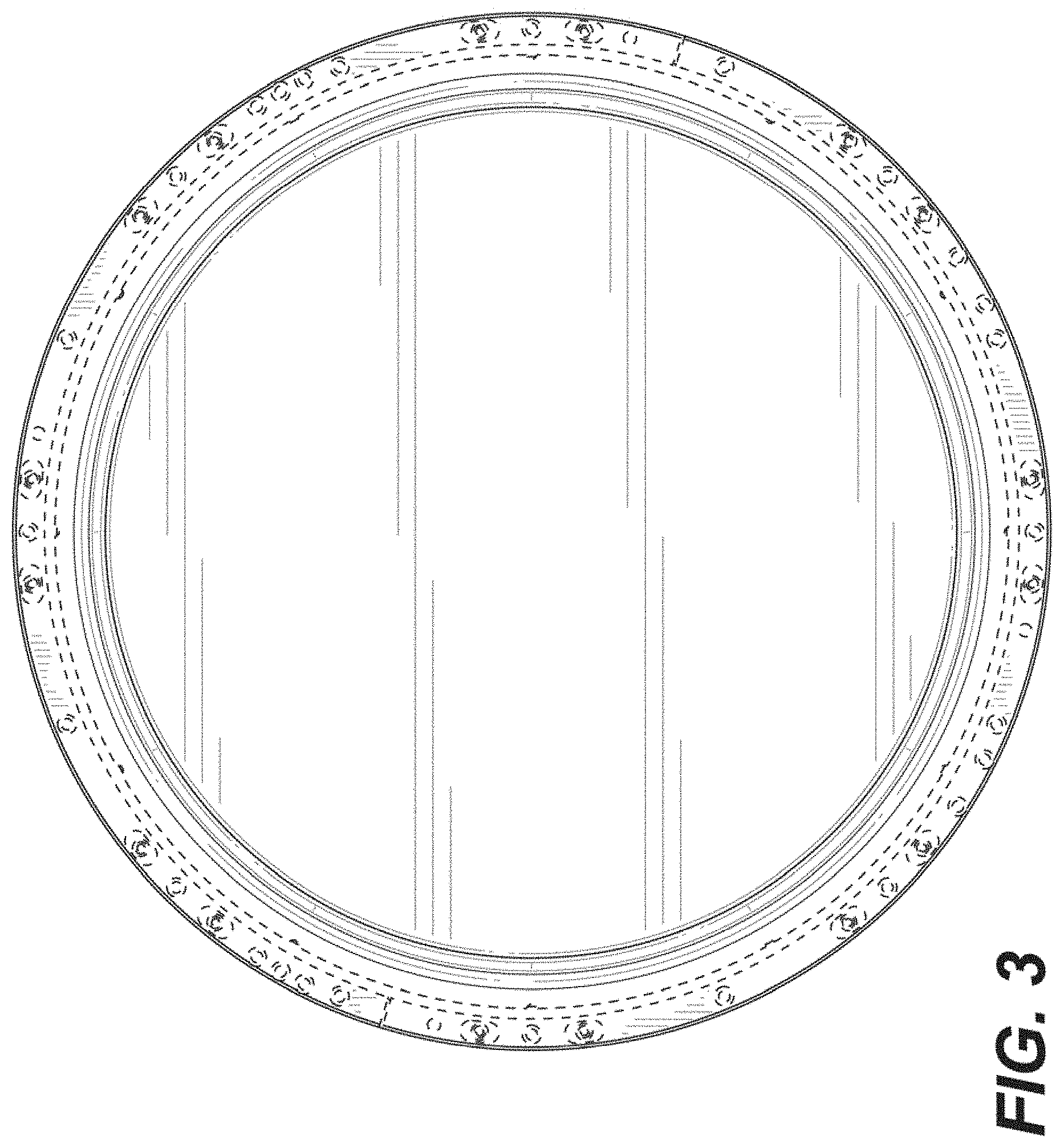
FIG. 3 is a top plan view thereof.
FIG. 4 is a bottom plan view thereof.
FIG. 5 is a right side plan view thereof.
FIG. 6 is a left side plan view thereof.
FIG. 7 is a front view thereof.
FIG. 8 is a back view thereof.
FIG. 9 is an enlarged cross sectional view taken along line 9-9 in FIG. 4.
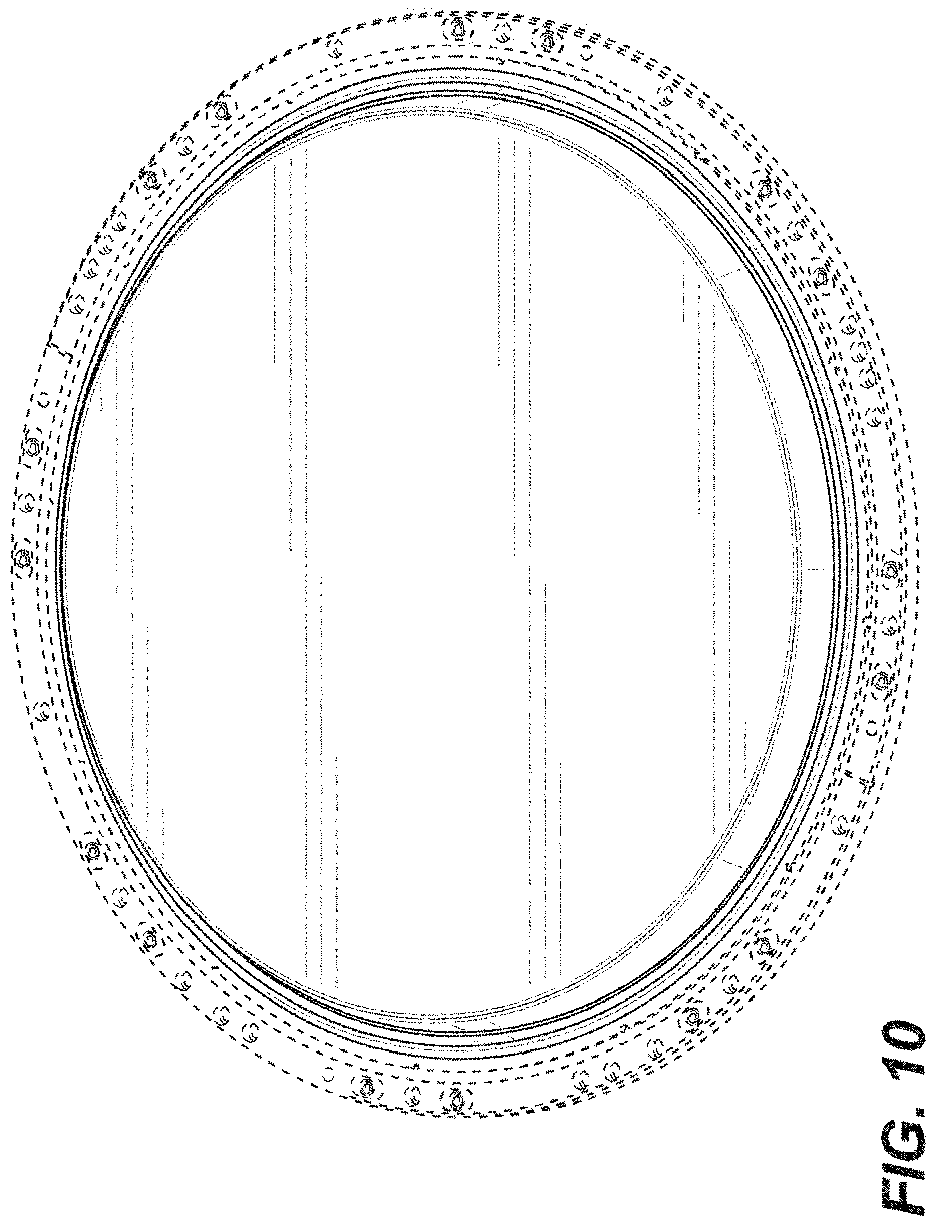
FIG. 10 is a top perspective view of a sputtering target for a physical vapor deposition chamber, according to another embodiment of the novel design.
FIG. 11 is a bottom perspective view thereof.
FIG. 12 is a top plan view thereof.
FIG. 13 is a bottom plan view thereof.
FIG. 14 is a right side plan view thereof.
FIG. 15 is a left side plan view thereof.
FIG. 16 is a front view thereof.
FIG. 17 is a back view thereof; and,
FIG. 18 is an enlarged cross sectional view taken along line 18-18 in FIG. 13.
The broken lines show portions of a sputtering target for a physical vapor deposition chamber which form no part of the claimed design.
* * * * *
References
D00000
D00001
D00002
D00003
D00004
D00005
D00006
D00007
D00008
D00009
D00010
D00011
D00012

XML
uspto.report is an independent third-party trademark research tool that is not affiliated, endorsed, or sponsored by the United States Patent and Trademark Office (USPTO) or any other governmental organization. The information provided by uspto.report is based on publicly available data at the time of writing and is intended for informational purposes only.
While we strive to provide accurate and up-to-date information, we do not guarantee the accuracy, completeness, reliability, or suitability of the information displayed on this site. The use of this site is at your own risk. Any reliance you place on such information is therefore strictly at your own risk.
All official trademark data, including owner information, should be verified by visiting the official USPTO website at www.uspto.gov. This site is not intended to replace professional legal advice and should not be used as a substitute for consulting with a legal professional who is knowledgeable about trademark law.