Lithographic apparatus and device manufacturing method
Lof , et al.
U.S. patent number 10,678,139 [Application Number 16/245,400] was granted by the patent office on 2020-06-09 for lithographic apparatus and device manufacturing method. This patent grant is currently assigned to ASML Netherlands B.V.. The grantee listed for this patent is ASML NETHERLANDS B.V.. Invention is credited to Erik Theodorus Maria Bijlaart, Hans Butler, Joannes Theodoor De Smit, Arie Jeffrey Den Boef, Sjoerd Nicolaas Lambertus Donders, Christiaan Alexander Hoogendam, Aleksey Yurievich Kolesnychenko, Mark Kroon, Joeri Lof, Erik Roelof Loopstra, Hendricus Johannes Maria Meijer, Jeroen Johannes Sophia Maria Mertens, Johannes Catherinus Hubertus Mulkens, Joost Jeroen Ottens, Roelof Aeilko Siebrand Ritsema, Timotheus Franciscus Sengers, Klaus Simon, Alexander Straaijer, Bob Streefkerk, Marcus Adrianus Van De Kerkhof, Helmar Van Santen, Frank Van Schaik.


| United States Patent | 10,678,139 |
| Lof , et al. | June 9, 2020 |
Lithographic apparatus and device manufacturing method
Abstract
A lithographic projection apparatus is disclosed in which a space between the projection system and a sensor is filled with a liquid.
| Inventors: | Lof; Joeri (Eindhoven, NL), Butler; Hans (Best, NL), Donders; Sjoerd Nicolaas Lambertus ('s-Hertogenbosch, NL), Kolesnychenko; Aleksey Yurievich (Helmond, NL), Loopstra; Erik Roelof (Heeze, NL), Meijer; Hendricus Johannes Maria (Veldhoven, NL), Mulkens; Johannes Catherinus Hubertus (Waalre, NL), Ritsema; Roelof Aeilko Siebrand (Eindhoven, NL), Van Schaik; Frank (Eindhoven, NL), Sengers; Timotheus Franciscus ('s-Hertogenbosch, NL), Simon; Klaus (Eindhoven, NL), De Smit; Joannes Theodoor (Eindhoven, NL), Straaijer; Alexander (Eindhoven, NL), Streefkerk; Bob (Tilburg, NL), Bijlaart; Erik Theodorus Maria (Rosmalen, NL), Hoogendam; Christiaan Alexander (Veldhoven, NL), Van Santen; Helmar (Amsterdam, NL), Van De Kerkhof; Marcus Adrianus (Helmond, NL), Kroon; Mark (Utrecht, NL), Den Boef; Arie Jeffrey (Waalre, NL), Ottens; Joost Jeroen (Veldhoven, NL), Mertens; Jeroen Johannes Sophia Maria (Duizel, NL) | ||||||||||
|---|---|---|---|---|---|---|---|---|---|---|---|
| Applicant: |
|
||||||||||
| Assignee: | ASML Netherlands B.V.
(Veldhoven, NL) |
||||||||||
| Family ID: | 34108333 | ||||||||||
| Appl. No.: | 16/245,400 | ||||||||||
| Filed: | January 11, 2019 |
Prior Publication Data
| Document Identifier | Publication Date | |
|---|---|---|
| US 20190250518 A1 | Aug 15, 2019 | |
Related U.S. Patent Documents
| Application Number | Filing Date | Patent Number | Issue Date | ||
|---|---|---|---|---|---|
| 15385584 | Dec 20, 2016 | 10180629 | |||
| 13306532 | Nov 29, 2011 | 9541843 | |||
| 12698932 | Feb 2, 2010 | 8482845 | |||
| 11482122 | Jul 7, 2006 | 8154708 | |||
| 10857614 | Jun 1, 2004 | 7213963 | |||
Foreign Application Priority Data
| Jun 9, 2003 [EP] | 03253636 | |||
| Aug 29, 2003 [EP] | 03255395 | |||
| Nov 10, 2003 [EP] | 03257068 | |||
| Current U.S. Class: | 1/1 |
| Current CPC Class: | G03F 7/70883 (20130101); G03F 7/70141 (20130101); G03F 7/70341 (20130101); G03F 7/7085 (20130101) |
| Current International Class: | G03F 7/20 (20060101) |
| Field of Search: | ;355/30,53 |
References Cited [Referenced By]
U.S. Patent Documents
| 3573975 | April 1971 | Dhaka et al. |
| 3648587 | March 1972 | Stevens |
| 3903413 | September 1975 | Manning |
| 4280054 | July 1981 | Guarino |
| 4346164 | August 1982 | Tabarelli et al. |
| 4358198 | November 1982 | Moriyama et al. |
| 4390273 | June 1983 | Loebach et al. |
| 4396705 | August 1983 | Akeyama et al. |
| 4465368 | August 1984 | Matsuura et al. |
| 4480910 | November 1984 | Takanashi et al. |
| 4509852 | April 1985 | Tabarelli et al. |
| 4540277 | September 1985 | Mayer et al. |
| 4853880 | August 1989 | Akamatsu et al. |
| 4887904 | December 1989 | Nakazato et al. |
| 4999669 | March 1991 | Sakamoto et al. |
| 5040020 | August 1991 | Rauschenbach et al. |
| 5121256 | June 1992 | Corle et al. |
| 5162642 | November 1992 | Akamatsu et al. |
| 5229872 | July 1993 | Mumola |
| 5243195 | September 1993 | Nishi |
| 5258823 | November 1993 | Akamatsu |
| 5296891 | March 1994 | Vogt et al. |
| 5517344 | May 1996 | Hu et al. |
| 5523193 | June 1996 | Nelson |
| 5528118 | June 1996 | Lee |
| 5610683 | March 1997 | Takahashi |
| 5623853 | April 1997 | Novak et al. |
| 5633968 | May 1997 | Sheem |
| 5654553 | August 1997 | Kawakubo et al. |
| 5668672 | September 1997 | Oomura |
| 5689377 | November 1997 | Takahashi |
| 5715039 | February 1998 | Fukuda et al. |
| 5825043 | October 1998 | Suwa |
| 5835275 | November 1998 | Takahashi et al. |
| 5874820 | February 1999 | Lee |
| 5883704 | March 1999 | Nishi et al. |
| 5900354 | May 1999 | Batchelder |
| 5969441 | October 1999 | Loopstra et al. |
| 5985496 | November 1999 | Okumura et al. |
| 5997963 | December 1999 | Davison et al. |
| 6031946 | February 2000 | Bergmann et al. |
| 6046792 | April 2000 | Van Der Werf et al. |
| 6078380 | June 2000 | Taniguchi et al. |
| 6137561 | October 2000 | Imai |
| 6191429 | February 2001 | Suwa |
| 6236634 | May 2001 | Lee et al. |
| 6333775 | December 2001 | Haney et al. |
| 6417914 | July 2002 | Li |
| 6560032 | May 2003 | Hatano |
| 6600547 | July 2003 | Watson et al. |
| 6603130 | August 2003 | Bisschops et al. |
| 6603530 | August 2003 | Kohno |
| 6618122 | September 2003 | Bisschops et al. |
| 6633365 | October 2003 | Suenaga |
| 6646729 | November 2003 | Van Der Laan et al. |
| 6650399 | November 2003 | Baselmans et al. |
| 6710849 | March 2004 | Kwan et al. |
| 6741331 | May 2004 | Boonman et al. |
| 6757048 | June 2004 | Arakawa |
| 6762826 | July 2004 | Tsukamoto et al. |
| 6784432 | August 2004 | Wieczorek |
| 6785006 | August 2004 | Nishida |
| 6787789 | September 2004 | Van Der Laan |
| 6788477 | September 2004 | Lin |
| 6801301 | October 2004 | Miyajima et al. |
| 6842256 | January 2005 | Hill |
| 6867844 | March 2005 | Vogel et al. |
| 6952253 | October 2005 | Lof et al. |
| 6954256 | October 2005 | Flagello et al. |
| 7009682 | March 2006 | Bleeker |
| 7075616 | July 2006 | Derksen et al. |
| 7081943 | July 2006 | Lof et al. |
| 7098991 | August 2006 | Nagasaka et al. |
| 7110081 | September 2006 | Hoogendam et al. |
| 7199858 | April 2007 | Lof et al. |
| 7213963 | May 2007 | Lof |
| 7224436 | May 2007 | Derksen et al. |
| 7227616 | June 2007 | Graeupner |
| 7372541 | May 2008 | Lof et al. |
| 7388648 | June 2008 | Lof et al. |
| 7486380 | February 2009 | Hazelton et al. |
| 7593093 | September 2009 | Lof et al. |
| 7760324 | July 2010 | Benschop et al. |
| 7843550 | November 2010 | Ishii et al. |
| 7932999 | April 2011 | Hoogendam et al. |
| 7982850 | July 2011 | Lof et al. |
| 8482845 | July 2013 | Lof et al. |
| 8797503 | August 2014 | Lof et al. |
| 9091940 | July 2015 | Derksen et al. |
| 9097987 | August 2015 | Hoogendam et al. |
| 9360765 | June 2016 | Hoogendam et al. |
| 9366972 | June 2016 | Lof et al. |
| 9482966 | November 2016 | Lof et al. |
| 9740107 | August 2017 | Lof et al. |
| 2001/0038442 | November 2001 | Hansell et al. |
| 2002/0018190 | February 2002 | Nogawa et al. |
| 2002/0020821 | February 2002 | Van Santen et al. |
| 2002/0026878 | March 2002 | Kwan et al. |
| 2002/0037461 | March 2002 | Van Der Werf et al. |
| 2002/0041377 | April 2002 | Hagiwara et al. |
| 2002/0057423 | May 2002 | Nogawa |
| 2002/0061469 | May 2002 | Tanaka |
| 2002/0079455 | June 2002 | Wieczorek |
| 2002/0081760 | June 2002 | Whatmore |
| 2002/0101574 | August 2002 | Tsuji |
| 2002/0118370 | August 2002 | Nishida |
| 2002/0145717 | October 2002 | Baselmans et al. |
| 2002/0163629 | November 2002 | Switkes et al. |
| 2002/0163630 | November 2002 | Bisschops et al. |
| 2002/0167642 | November 2002 | Jones et al. |
| 2002/0167651 | November 2002 | Boonman et al. |
| 2002/0196421 | December 2002 | Tanaka et al. |
| 2003/0030916 | February 2003 | Suenaga |
| 2003/0071982 | April 2003 | Miyajima et al. |
| 2003/0095244 | May 2003 | Komatsu |
| 2003/0123040 | July 2003 | Almogy |
| 2003/0174408 | September 2003 | Rostalski et al. |
| 2003/0213921 | November 2003 | Van De Moosdijk et al. |
| 2004/0000627 | January 2004 | Schuster |
| 2004/0021844 | February 2004 | Suenaga |
| 2004/0036850 | February 2004 | Tsukamoto et al. |
| 2004/0069329 | April 2004 | de Larios et al. |
| 2004/0075895 | April 2004 | Lin |
| 2004/0108467 | June 2004 | Eurlings et al. |
| 2004/0109237 | June 2004 | Epple et al. |
| 2004/0114117 | June 2004 | Bleeker |
| 2004/0114124 | June 2004 | Hoeks et al. |
| 2004/0118184 | June 2004 | Violette |
| 2004/0119954 | June 2004 | Kawashima et al. |
| 2004/0125351 | July 2004 | Krautschik |
| 2004/0135099 | July 2004 | Simon et al. |
| 2004/0136494 | July 2004 | Lof et al. |
| 2004/0160582 | August 2004 | Lof et al. |
| 2004/0165159 | August 2004 | Lof et al. |
| 2004/0169834 | September 2004 | Richter et al. |
| 2004/0169924 | September 2004 | Flagello et al. |
| 2004/0180294 | September 2004 | Baba-Ali et al. |
| 2004/0180299 | September 2004 | Rolland et al. |
| 2004/0207824 | October 2004 | Lof et al. |
| 2004/0211920 | October 2004 | Derksen et al. |
| 2004/0224265 | November 2004 | Endo et al. |
| 2004/0224525 | November 2004 | Endo et al. |
| 2004/0227923 | November 2004 | Flagello et al. |
| 2004/0233405 | November 2004 | Kato et al. |
| 2004/0253547 | December 2004 | Endo et al. |
| 2004/0253548 | December 2004 | Endo et al. |
| 2004/0257544 | December 2004 | Vogel et al. |
| 2004/0259008 | December 2004 | Endo et al. |
| 2004/0259040 | December 2004 | Endo et al. |
| 2004/0263808 | December 2004 | Sewell |
| 2004/0263809 | December 2004 | Nakano |
| 2005/0002004 | January 2005 | Kolesnychenko et al. |
| 2005/0007569 | January 2005 | Streefkerk et al. |
| 2005/0007570 | January 2005 | Streefkerk et al. |
| 2005/0018155 | January 2005 | Cox et al. |
| 2005/0018156 | January 2005 | Mulkens et al. |
| 2005/0024609 | February 2005 | De Smit et al. |
| 2005/0030497 | February 2005 | Nakamura |
| 2005/0030498 | February 2005 | Mulkens |
| 2005/0030506 | February 2005 | Schuster |
| 2005/0036121 | February 2005 | Hoogendam et al. |
| 2005/0036183 | February 2005 | Yeo et al. |
| 2005/0036184 | February 2005 | Yeo et al. |
| 2005/0036213 | February 2005 | Mann et al. |
| 2005/0037269 | February 2005 | Levinson |
| 2005/0041225 | February 2005 | Sengers et al. |
| 2005/0042554 | February 2005 | Dierichs et al. |
| 2005/0046813 | March 2005 | Streefkerk et al. |
| 2005/0046934 | March 2005 | Ho et al. |
| 2005/0048223 | March 2005 | Pawloski et al. |
| 2005/0052632 | March 2005 | Miyajima |
| 2005/0068639 | March 2005 | Pierrat et al. |
| 2005/0073670 | April 2005 | Carroll |
| 2005/0078287 | April 2005 | Sengers et al. |
| 2005/0084794 | April 2005 | Meagley et al. |
| 2005/0094116 | May 2005 | Flagello et al. |
| 2005/0099635 | May 2005 | Kakuchi et al. |
| 2005/0100745 | May 2005 | Lin et al. |
| 2005/0110973 | May 2005 | Streefkerk et al. |
| 2005/0117224 | June 2005 | Shafer et al. |
| 2005/0122497 | June 2005 | Lyons et al. |
| 2005/0122505 | June 2005 | Miyajima |
| 2005/0132914 | June 2005 | Mulkens et al. |
| 2005/0134815 | June 2005 | Van Santen et al. |
| 2005/0134817 | June 2005 | Nakamura |
| 2005/0141098 | June 2005 | Schuster |
| 2005/0145265 | July 2005 | Ravkin et al. |
| 2005/0145803 | July 2005 | Hakey et al. |
| 2005/0146694 | July 2005 | Tokita |
| 2005/0146695 | July 2005 | Kawakami |
| 2005/0147920 | July 2005 | Lin et al. |
| 2005/0153424 | July 2005 | Coon |
| 2005/0158673 | July 2005 | Hakey et al. |
| 2005/0164502 | July 2005 | Deng et al. |
| 2005/0174549 | August 2005 | Duineveld et al. |
| 2005/0175940 | August 2005 | Dierichs |
| 2005/0185269 | August 2005 | Epple et al. |
| 2005/0190435 | September 2005 | Shafer et al. |
| 2005/0190455 | September 2005 | Rostalski et al. |
| 2005/0205108 | September 2005 | Chang et al. |
| 2005/0213061 | September 2005 | Hakey et al. |
| 2005/0213072 | September 2005 | Schenker et al. |
| 2005/0217135 | October 2005 | O'Donnell et al. |
| 2005/0217137 | October 2005 | Smith et al. |
| 2005/0217703 | October 2005 | O'Donnell |
| 2005/0219481 | October 2005 | Cox et al. |
| 2005/0219482 | October 2005 | Baselmans et al. |
| 2005/0219499 | October 2005 | Maria Zaal et al. |
| 2005/0225734 | October 2005 | De Smit et al. |
| 2005/0226737 | October 2005 | Weissenrieder et al. |
| 2005/0231694 | October 2005 | Kolesnychenko et al. |
| 2005/0237501 | October 2005 | Furukawa et al. |
| 2005/0243292 | November 2005 | Baselmans et al. |
| 2005/0243328 | November 2005 | Wegmann et al. |
| 2005/0245005 | November 2005 | Benson |
| 2005/0253090 | November 2005 | Gau et al. |
| 2005/0259232 | November 2005 | Streefkerk et al. |
| 2005/0259233 | November 2005 | Streefkerk et al. |
| 2005/0259234 | November 2005 | Hirukawa et al. |
| 2005/0264778 | December 2005 | Lof et al. |
| 2005/0270505 | December 2005 | Smith |
| 2006/0023186 | February 2006 | Binnard |
| 2006/0103832 | May 2006 | Hazelton et al. |
| 2006/0114445 | June 2006 | Ebihara |
| 2006/0170891 | August 2006 | Nishinaga et al. |
| 2006/0181690 | August 2006 | Nishinaga et al. |
| 2006/0209414 | September 2006 | Van Santen et al. |
| 2006/0261288 | November 2006 | Van Santen |
| 2006/0285100 | December 2006 | Hamatani et al. |
| 2007/0013888 | January 2007 | Flagello et al. |
| 2007/0076181 | April 2007 | Ishii et al. |
| 2007/0076182 | April 2007 | Hazelton et al. |
| 2007/0132970 | June 2007 | Lof et al. |
| 2007/0146665 | June 2007 | Ottens et al. |
| 2007/0177125 | August 2007 | Shibazaki |
| 2007/0247602 | October 2007 | Binnard |
| 2007/0268471 | November 2007 | Lof et al. |
| 2009/0279061 | November 2009 | Jacobs et al. |
| 2013/0250270 | September 2013 | Lof et al. |
| 2017/0010545 | January 2017 | Lof et al. |
| 2017/0102621 | April 2017 | Lof et al. |
| 1341277 | Mar 2002 | CN | |||
| 206 607 | Feb 1984 | DE | |||
| 221 563 | Apr 1985 | DE | |||
| 224448 | Jul 1985 | DE | |||
| 242880 | Feb 1987 | DE | |||
| 0023231 | Feb 1981 | EP | |||
| 0418427 | Mar 1991 | EP | |||
| 0 605 103 | Jul 1994 | EP | |||
| 0 834 773 | Apr 1998 | EP | |||
| 10-154659 | Jun 1998 | EP | |||
| 1039511 | Sep 2000 | EP | |||
| 1 82 511 | Feb 2002 | EP | |||
| 1 477 856 | Nov 2004 | EP | |||
| 1 494 267 | Jan 2005 | EP | |||
| 1 571 696 | Sep 2005 | EP | |||
| 1 571 701 | Sep 2005 | EP | |||
| 1 628 329 | Feb 2006 | EP | |||
| 2474708 | Jul 1981 | FR | |||
| 57-153433 | Sep 1982 | JP | |||
| 58-202448 | Nov 1983 | JP | |||
| 59-19912 | Feb 1984 | JP | |||
| 62-065326 | Mar 1987 | JP | |||
| 62-121417 | Jun 1987 | JP | |||
| 63-157419 | Jun 1988 | JP | |||
| 2-47515 | Feb 1990 | JP | |||
| 04-305915 | Oct 1992 | JP | |||
| 04-305917 | Oct 1992 | JP | |||
| 5-62877 | Mar 1993 | JP | |||
| 5-251544 | Sep 1993 | JP | |||
| 5-304072 | Nov 1993 | JP | |||
| 06-84757 | Mar 1994 | JP | |||
| 06-124873 | May 1994 | JP | |||
| 06-168866 | Jun 1994 | JP | |||
| 6-168866 | Jun 1994 | JP | |||
| 07-132262 | May 1995 | JP | |||
| 07-220990 | Aug 1995 | JP | |||
| 08-316125 | Nov 1996 | JP | |||
| 09-066429 | Mar 1997 | JP | |||
| 09-184787 | Jul 1997 | JP | |||
| 10-92728 | Apr 1998 | JP | |||
| 10-135316 | May 1998 | JP | |||
| 10-160582 | Jun 1998 | JP | |||
| 10-228661 | Aug 1998 | JP | |||
| 10-255319 | Sep 1998 | JP | |||
| 10-303114 | Nov 1998 | JP | |||
| 10-340846 | Dec 1998 | JP | |||
| 11-126112 | May 1999 | JP | |||
| 11-176727 | Jul 1999 | JP | |||
| H11-239758 | Sep 1999 | JP | |||
| 11-297615 | Oct 1999 | JP | |||
| 2000-058436 | Feb 2000 | JP | |||
| 2000-097616 | Apr 2000 | JP | |||
| 2000-331931 | Nov 2000 | JP | |||
| 2001-091849 | Apr 2001 | JP | |||
| 2001-281050 | Oct 2001 | JP | |||
| 2002-5737 | Jan 2002 | JP | |||
| 2002-071513 | Mar 2002 | JP | |||
| 2002-071514 | Mar 2002 | JP | |||
| 2002-513856 | May 2002 | JP | |||
| 2002-170754 | Jun 2002 | JP | |||
| 2002-170765 | Jun 2002 | JP | |||
| 2002-246309 | Aug 2002 | JP | |||
| 2002-250678 | Sep 2002 | JP | |||
| 2002-296005 | Oct 2002 | JP | |||
| 2003-332213 | Nov 2003 | JP | |||
| 2004-165666 | Jun 2004 | JP | |||
| 2004-193252 | Jul 2004 | JP | |||
| 2004-289126 | Oct 2004 | JP | |||
| 2005-012201 | Jan 2005 | JP | |||
| 2005-101488 | Apr 2005 | JP | |||
| 2005-223275 | Aug 2005 | JP | |||
| 2005-277363 | Oct 2005 | JP | |||
| 1 628 330 | Feb 2006 | JP | |||
| 2006-523377 | Oct 2006 | JP | |||
| 2007-142460 | Jun 2007 | JP | |||
| 4362867 | Nov 2009 | JP | |||
| 2010-135857 | Jun 2010 | JP | |||
| 98/33096 | Jul 1998 | WO | |||
| 98/38597 | Sep 1998 | WO | |||
| 98/38597 | Sep 1998 | WO | |||
| 98/40791 | Sep 1998 | WO | |||
| 99/39375 | Aug 1999 | WO | |||
| 99/49504 | Sep 1999 | WO | |||
| 99/060361 | Nov 1999 | WO | |||
| 01/22480 | Mar 2001 | WO | |||
| 02/090905 | Nov 2002 | WO | |||
| 02/091078 | Nov 2002 | WO | |||
| 03/077036 | Sep 2003 | WO | |||
| 03/077037 | Sep 2003 | WO | |||
| 03/085708 | Oct 2003 | WO | |||
| 2004/019128 | Mar 2004 | WO | |||
| 2004/053596 | Jun 2004 | WO | |||
| 2004/053950 | Jun 2004 | WO | |||
| 2004/053951 | Jun 2004 | WO | |||
| 2004/053952 | Jun 2004 | WO | |||
| 2004/053953 | Jun 2004 | WO | |||
| 2004/053954 | Jun 2004 | WO | |||
| 2004/053955 | Jun 2004 | WO | |||
| 2004/053956 | Jun 2004 | WO | |||
| 2004/053957 | Jun 2004 | WO | |||
| 2004/053958 | Jun 2004 | WO | |||
| 2004/053959 | Jun 2004 | WO | |||
| 2004/055803 | Jul 2004 | WO | |||
| 2004/057295 | Jul 2004 | WO | |||
| 2004/057589 | Jul 2004 | WO | |||
| 2004/057590 | Jul 2004 | WO | |||
| 2004/077154 | Sep 2004 | WO | |||
| 2004/081666 | Sep 2004 | WO | |||
| 2004/090577 | Oct 2004 | WO | |||
| 2004/090633 | Oct 2004 | WO | |||
| 2004/090634 | Oct 2004 | WO | |||
| 2004/092830 | Oct 2004 | WO | |||
| 2004/092833 | Oct 2004 | WO | |||
| 2004/093130 | Oct 2004 | WO | |||
| 2004/093159 | Oct 2004 | WO | |||
| 2004/093160 | Oct 2004 | WO | |||
| 2004/095135 | Nov 2004 | WO | |||
| 2004/105107 | Dec 2004 | WO | |||
| 2004/112108 | Dec 2004 | WO | |||
| 2005/001432 | Jan 2005 | WO | |||
| 2005/001572 | Jan 2005 | WO | |||
| 2005/003864 | Jan 2005 | WO | |||
| 2005/006026 | Jan 2005 | WO | |||
| 2005/008339 | Jan 2005 | WO | |||
| 2005/010611 | Feb 2005 | WO | |||
| 2005/013008 | Feb 2005 | WO | |||
| 2005/015283 | Feb 2005 | WO | |||
| 2005/017625 | Feb 2005 | WO | |||
| 2005/019935 | Mar 2005 | WO | |||
| 2005/022266 | Mar 2005 | WO | |||
| 2005/022616 | Mar 2005 | WO | |||
| 2005/024325 | Mar 2005 | WO | |||
| 2005/024517 | Mar 2005 | WO | |||
| 2005/034174 | Apr 2005 | WO | |||
| 2005/050324 | Jun 2005 | WO | |||
| 2005/054953 | Jun 2005 | WO | |||
| 2005/054955 | Jun 2005 | WO | |||
| 2005/059617 | Jun 2005 | WO | |||
| 2005/059618 | Jun 2005 | WO | |||
| 2005/059645 | Jun 2005 | WO | |||
| 2005/059654 | Jun 2005 | WO | |||
| 2005/062128 | Jul 2005 | WO | |||
| 2005/064400 | Jul 2005 | WO | |||
| 2005/064405 | Jul 2005 | WO | |||
| 2005/069055 | Jul 2005 | WO | |||
| 2005/069078 | Jul 2005 | WO | |||
| 2005/069081 | Jul 2005 | WO | |||
| 2005/071491 | Aug 2005 | WO | |||
| 2005/074606 | Aug 2005 | WO | |||
| 2005/076084 | Aug 2005 | WO | |||
| 2005/081030 | Sep 2005 | WO | |||
| 2005/081067 | Sep 2005 | WO | |||
| 2005/098504 | Oct 2005 | WO | |||
| 2005/098505 | Oct 2005 | WO | |||
| 2005/098506 | Oct 2005 | WO | |||
| 2005/106589 | Nov 2005 | WO | |||
| 2005/111689 | Nov 2005 | WO | |||
| 2005/111722 | Nov 2005 | WO | |||
| 2005/119368 | Dec 2005 | WO | |||
| 2005/119369 | Dec 2005 | WO | |||
Other References
|
US. Office Action issued in corresponding U.S. Appl. No. 16/229,102, dated Apr. 19, 2019. cited by applicant . U.S. Notice of Allowance issued in corresponding U.S. Appl. No. 14/937,724, dated May 1, 2019. cited by applicant . Information Disclosure Statement filed Dec. 1, 2006 for U.S. Appl. No. 11/606,913. cited by applicant . Information Disclosure Statement filed Dec. 1, 2006 for U.S. Appl. No. 11/606,909. cited by applicant . Office Action dated Apr. 6, 2007 issued for U.S. Appl. No. 11/606,913. cited by applicant . Office Action dated Nov. 6, 2006 issued for U.S. Appl. No. 11/002,900. cited by applicant . Office Action dated May 22, 2006 issued for U.S. Appl. No. 11/002,900. cited by applicant . Third Preliminary Amendment dated Aug. 17, 2005 for U.S. Appl. No. 11/147,285. cited by applicant . Office Action dated Sep. 29, 2008 issued for U.S. Appl. No. 11/606,909. cited by applicant . Office Action dated Dec. 28, 2007 issued for U.S. Appl. No. 11/606,913. cited by applicant . Office Action dated Sep. 17, 2007 issued for U.S. Appl. No. 11/002,900. cited by applicant . Emerging Lithographic Technologies VI, Proceedings of SPIE, vol. 4688 (2002), "Semiconductor Foundry, Lithography, and Partners", B.J. Lin, pp. 11-24. cited by applicant . Optical Microlithography XV, Proceedings of SPIE, vol. 4691 (2002), "Resolution Enhancement of 157 nm Lithography by Liquid Immersion", M. Switkes et al., pp. 459-465. cited by applicant . J. Microlith., Microfab., Microsyst., vol. 1 No. 3, Oct. 2002, Society of Photo-Optical Instrumentation Engineers, "Resolution enhancement of 157 nm lithography by liquid immersion", M. Switkes et al., pp. 1-4. cited by applicant . S. Owa et al., "Immersion lithography; its potential performance and issues", Proceedings of SPIE vol. 5040, 2003, pp. 724-733. cited by applicant . European Search Report for EP 02257938 dated Sep. 25, 2003. cited by applicant . M. Switkes et al., "Immersion Lithography at 157 nm," MIT Lincoln Lab, Orlando Jan. 2001, Dec. 17, 2001. cited by applicant . M. Switkes et al., "Immersion Lithography at 157 nm," J. Vac. Sci. Technol. B., vol. 19, No. 6, Nov./Dec. 2001, pp. 2353-2356. cited by applicant . M. Switkes et al., "Immersion Lithography: Optics for the 50 nm Node," 157 Anvers-1, Sep. 4, 2002. cited by applicant . B.J. Lin, "Drivers, Prospects and Challenges for Immersion Lithography," TSMC, Inc., Sep. 2002. cited by applicant . B.J. Lin, "Proximity Printing Through Liquid," IBM Technical Disclosure Bulletin, vol. 20, No. 11B, Apr. 1978, p. 4997. cited by applicant . B.J. Lin, "The Paths to Subhalf-Micrometer Optical Lithography," SPIE vol. 922, Optical/Laser Microlithography (1988), pp. 256-269. cited by applicant . G.W.W. Stevens, "Reduction of Waste Resulting from Mask Defects," Solid State Technology, Aug. 1978, vol. 21 008, pp. 68-72. cited by applicant . S. Owa et al., "Advantage and Feasibility of Immersion Lithography," Proc. SPIE 5040 (2003). cited by applicant . Nikon Precision Europe GmbH, "Investor Relations--Nikon's Real Solutions," May 15, 2003. cited by applicant . H. Kawata et al., "Optical Projection Lithography using Lenses with Numerical Apertures Greater than Unity," Microelectronic Engineering 9 (1989), pp. 31-36. cited by applicant . J.A. Hoffnagle et al., "Liquid Immersion Deep-Ultraviolet Interferometric Lithography," J. Vac. Sci. Technol. B., vol. 17, No. 6, Nov./Dec. 1999, pp. 3306-3309. cited by applicant . B.W. Smith et al., "Immersion Optical Lithography at 193 nm," Future Fab International, vol. 15, Jul. 11, 2003. cited by applicant . H. Kawata et al., "Fabrication of 0.2.mu.m Fine Patterns Using Optical Projection Lithography with an Oil Immersion Lens," Jpn. J. Appl. Phys. vol. 31 (1992), pp. 4174-4177. cited by applicant . G. Owen et al., "1/8.mu.m Optical Lithography," J. Vac. Sci. Technol. B., vol. 10, No. 6, Nov./Dec. 1992, pp. 3032-3036. cited by applicant . H. Hogan, "New Semiconductor Lithography Makes a Splash," Photonics Spectra, Photonics Technology World, Oct. 2003 Edition, pp. 1-3. cited by applicant . S. Owa and N. Nagasaka, "Potential Performance and Feasibility of Immersion Lithography," NGL Workshop 2003, Jul. 10, 2003, Slide Nos. 1-33. cited by applicant . European Search Report dated May 3, 2004 for EP 03257068.1. cited by applicant . S. Owa et al., "Update on 193nm immersion exposure tool," Litho Forum, International SEMATECH, Los Angeles, Jan. 27-29, 2004, Slide Nos. 1-51. cited by applicant . H. Hata, "The Development of Immersion Exposure Tools," Litho Forum, International Sematech, Los Angeles, Jan. 27-29, 2004, Slide Nos. 1-22. cited by applicant . T. Matsuyama et al., "Nikon Projection Lens Update," SPIE Microlithography 2004, 5377-65, Mar. 2004. cited by applicant . "Depth-of-Focus Enhancement Using High Refractive Index Layer on the Imaging Layer," IBM Technical Disclosure Bulletin, vol. 27, No. 11, Apr. 1985, p. 6521. cited by applicant . A. Suzuki, "Lithography Advances on Multiple Fronts," EEdesign, EE Times, Jan. 5, 2004. cited by applicant . B.J. Lin, "The k.sub.3 coefficient in nonparaxial .lamda./NA scaling equations for resolution, depth of focus, and immersion lithography," J. Microlith., Microfab., Microsyst., 1(1):7-12 (2002). cited by applicant . European Search Report for EP 03257068 completed Aug. 17, 2004. cited by applicant . Examination Report for EP Patent Appln. No. 03257072.3 dated Mar. 28, 2008. cited by applicant . European Search Report for EP Patent Appln. No. 03257068.1 dated May 3, 2004. cited by applicant . European Search Report for EP Patent Appln. No. 03255395.0 dated Aug. 19, 2004. cited by applicant . Japanese Office Action issued for Japanese Patent Application No. 2003-417260, dated Dec. 18, 2006. cited by applicant . Japanese Official Action issued for Japanese Patent Application No. 2004-169275, dated Jul. 12, 2007. cited by applicant . English Translation of JP 10-228661 (dated Aug. 25, 1998). cited by applicant . European Office Action dated Jan. 3, 2012 in corresponding European Patent. cited by applicant . U.S. Office Action dated Sep. 25, 2012 in corresponding U.S. Patent Application No. cited by applicant . U.S. Office Action dated Sep. 27, 2012 in corresponding U.S. Appl. No. 12/698,932. cited by applicant . Japanese Office Action dated Jul. 24, 2012 in corresponding Japanese Patent Application No. 2011-243516. cited by applicant . U.S. Office Action dated Mar. 4, 2013 in corresponding U.S. Appl. No. 12/850,472. cited by applicant . U.S. Office Action dated May 28, 2013 in corresponding U.S. Appl. No. 13/149,404. cited by applicant . Japanese Office Action dated Jun. 12, 2013 in corresponding Japanese Patent Application No. 2012-027270. cited by applicant . Japanese Office Action dated May 31, 2013 in corresponding Japanese Patent Application No. 2011-281445. cited by applicant . U.S. Office Action dated Aug. 8, 2013 in corresponding U.S. Appl. No. 13/195,248. cited by applicant . U.S. Office Action dated Aug. 8, 2013 in corresponding U.S. Appl. No. 13/194,136. cited by applicant . Chinese Office Action dated Jul. 1, 2013 in corresponding Chinese Patent Application No. 201110083335.0. cited by applicant . U.S. Office Action dated Oct. 25, 2013 in corresponding U.S. Appl. No. 13/722,830. cited by applicant . U.S. Office Action dated Sep. 9, 2013 in corresponding U.S. Appl. No. 13/149,404. cited by applicant . Singapore Search Report and Written Opinion dated Nov. 4, 2013 in corresponding Singapore Patent Application No. 201005011-0. cited by applicant . U.S. Office Action dated Nov. 12, 2013 in corresponding U.S. Appl. No. 13/195,248. cited by applicant . U.S. Office Action dated Nov. 15, 2013 in corresponding U.S. Appl. No. 13/194,136. cited by applicant . U.S. Office Action dated Nov. 20, 2013 in corresponding U.S. Appl. No. 12/512,754. cited by applicant . Japanese Office Action dated Nov. 8, 2013 in corresponding Japanese Patent Application No. 2012-066781. cited by applicant . U.S. Office Action dated Feb. 24, 2014 in corresponding U.S. Appl. No. 13/722,830. cited by applicant . U.S. Official Action dated Mar. 17, 2014 in corresponding U.S. Appl. No. 13/149,404. cited by applicant . U.S. Office Action dated Apr. 3, 2014 in corresponding U.S. Appl. No. 12/512,754. cited by applicant . U.S. Office Action dated Apr. 4, 2014 in corresponding U.S. Appl. No. 13/195,248. cited by applicant . U.S. Office Action dated Apr. 3, 2014 in corresponding U.S. Appl. No. 13/194,136. cited by applicant . U.S. Office Action dated Aug. 21, 2014 in corresponding U.S. Appl. No. 13/194,136. cited by applicant . U.S. Official Action dated Dec. 31, 2014 in corresponding U.S. Appl. No. 13/692,865. cited by applicant . U.S. Office Action dated Apr. 2, 2015 in corresponding U.S. Appl. No. 13/615,190. cited by applicant . V. LeRoux et al., "A reflection lithography using multicharged ions," Microelectronic Engineering, vol. 57-58, pp. 239-245 (Sep. 2001). cited by applicant . Ivor Brodie et al., "A Multiple-Electron-Beam Exposure System for High-Throughput, Direct-Write Submicrometer Lithography," IEEE Transactions on Electron Devices, vol. EDS-28, No. 11, pp. 1422-1428 (Nov. 1981). cited by applicant . Yuen-Chuen Chan et al., "Development and applications of a laser writing lithography system for maskless patterning," Opt. Eng., vol. 37, No. 9, pp. 2521-2530 (Sep. 1998). cited by applicant . W. Ha er-Grohne et al., "An electron optical metrology system for pattern placement measurements," Meas. Sci. Technol., vol. 9, pp. 1120-1128 (1998). cited by applicant . Shoji Maruo et al., "Submicron stereolithography for the production of freely movable mechanisms by using single-photon polymerization," Sensors and Actuators A, vol. 100, pp. 70-76 (Aug. 2002). cited by applicant . F. Abboud et al., "Evaluation of the MEBES.RTM. 4500 reticle writer to commercial requirements of 250 nm design rule IC devices," Proc of SPIE, vol. 2793, pp. 438-451 (Jul. 24, 1996). cited by applicant . Toru Tojo et al., "Advanced electron beam writing system EX-11 for next-generation mask fabrication," Proc. of SPIE, vol. 3748, pp. 416-425 (Sep. 1999). cited by applicant . Yoshiyuki Tomita et al., "A surface motor-driven precise positioning system," Precision Engineering, vol. 16, No. 3, pp. 184-191 (Jul. 1994). cited by applicant . Chang-Woo Lee et al., "An ultraprecision stage for alignment of wafers in advanced microlithography," Precision Engineering, vol. 21, No, 2/3, pp. 113-122, (Sep./Dec. 1997). cited by applicant . H. Loschner et al., "Ion projection lithography for vacuum microelectronics," J. Vac. Sci. Technol, B, vol. 11, No. 2, pp. 487-492 (Mar./Apr. 1993). cited by applicant . Hans Loeschner et al., "Large-Field Ion-Optics for Projection and Proximity Printing and for Mask-Less Lithography (ML2)," Proc. of SPIE, vol. 4688, pp. 595-606 (Jul. 2002). cited by applicant . Won-jong Kim et al., "Modeling and Vector Control of Planar Magnetic Levitator," IEEE Transactions on Industry Applications, vol. 34, No. 6, pp. 1254-1262 (Nov./ Dec. 1998). cited by applicant . Rodney Kendall et al., "A servo guided X-Y-theta stage for electron beam lithography," J. Vac. Sci. Technol. B, vol. 9, No. 6, pp. 3019-3023 (Nov./Dec. 1991). cited by applicant . T. Kato et al., "Submicron pattern fabrication by focused Ion beams," J. Vac. Sci. Technol. B, vol. 3, No. 1, pp. 50-53 (Jan./Feb. 1985). cited by applicant . Hans C. Pfeiffer, "PREVAIL: Proof-of-Concept System and Results," Microelectronic Engineering, vol. 53, pp. 61-66 (2000). cited by applicant . L.M. Buchmann et al., "Lithography with High Depth of Focus by an Ion Projection System," Journal of Microelectromechanical Systems, vol. 1, No. 3, pp. 116-120 (Sep. 1992). cited by applicant . T.C. Bailey et al., "Step and Flash Imprint Lithography: An Efficient Nanoscale Printing Technology," Journal of Photopolymer Science and Technology, vol. 15, No. 3, pp. 481-486 (Jan. 2002). cited by applicant . Oui-Serg Kim et al., "Positioning Performance and Straightness Error Compensation of the Magnetic Levitation Stage Supported by the Linear Magnetic Bearing," IEEE Transactions on Industrial Electronics, vol. 50, No. 2, pp. 374-378 (Apr. 2003). cited by applicant . Ampere A. Tseng et al., "Electron Beam Lithography in Nanoscale Fabrication: Recent Development," IEEE Transactions on Electronics Packaging Manufacturing, vol. 26, No. 2, pp. 141-149 (Apr. 2003). cited by applicant . Qing Ji, "Maskless, Resistless Ion Beam Lithography Processes," University of Berkeley, 128 pages (Spring 2003). cited by applicant . Rlk Kneppers, "HP Laser Interferometers," Vaisala News, vol. 151, pp. 34-37 (1999). cited by applicant . R.S. Dhaliwal et al., "PREVAIL--Electron projection technology approach for next-generation lithography," IBM J. Res. & Dev., vol. 45, No. 5, pp. 615-638 (Sep. 2001). cited by applicant . Kazuaki Suzuki, "EPL Technology Development," Proc. of SPIE, vol. 4754, pp. 775-789 (Jul. 2002). cited by applicant . G. Stengl et al., "Current status of Ion Projection Lithography," Proc. of SPIE, vol. 537, pp. 138-145 (1985). cited by applicant . Ernst Thielicke et al., "Microactuators and their technologies," Mechatronics, vol. 10, pp. 431-455 (2000). cited by applicant . G. Stangl et al., "Submicron Lithography and DUV-Master Masks Made by Ion Projection Lithography," Microelectronic Engineering, vol. 3, pp. 167-171 (1985). cited by applicant . G. Stengl et al., "Ion projection lithography machine IPLM01: A new tool for sub-0.5-micron modification of materials," J. Vac. Sci. Technol. B, vol. 4, No. 1, pp. 194-200 (Jan./Feb. 1986). cited by applicant . Carl G. Chen et al., "Nanometer-accurate Grating Fabrication with Scanning Beam Interference Lithography," Proc. of SPIE, vol. 4936, pp. 126-134 (Nov. 2002). cited by applicant . G. de Zwart et al., "Performance of a Step and Scan System for DUV Lithography," SPIE Symposium on Optical Microlithography in Santa Clara, pp. 0-18 (Mar. 1997). cited by applicant . Jan Mulkens et al., "ASML Optical Lithography Solutions for 65 nm and 45 nm Node," Semicon Japan, pp. 1-29, (Dec. 5, 2003). cited by applicant . Arnold et al., "193nm Immersion Lithography," International Sematech Litho Forum, Slides 1-22, (Jan. 28, 2004). cited by applicant . U.S. Office Action dated Sep. 30, 2015 in corresponding U.S. Appl. No. 13/615,190. cited by applicant . U.S. Office Action dated Oct. 7, 2015 in corresponding U.S. Appl. No. 14/816,997. cited by applicant . U.S. Office Action dated Oct. 7, 2015 in corresponding U.S. Appl. No. 14/701,236. cited by applicant . U.S. Office Action dated Jun. 29, 2016 in corresponding U.S. Appl. No. 15/167,357. cited by applicant . U.S. Office Action dated Oct. 20, 2016 in corresponding U.S. Appl. No. 15/178,522. cited by applicant . Japanese Office Action dated Nov. 6, 2012 in corresponding Japanese Patent Application No. 2011-243513. cited by applicant . U.S. Office Action dated Nov. 26, 2012 in corresponding U.S. Appl. No. 12/698,938. cited by applicant . U.S. Office Action dated Oct. 24, 2012 in corresponding U.S. Appl. No. 12/512,754. cited by applicant . U.S. Office Action dated Oct. 15, 2012 in corresponding U.S. Appl. No. 13/149,404. cited by applicant . U.S. Office Action dated Jan. 18, 2017 in corresponding U.S. Appl. No. 14/743,775. cited by applicant . U.S. Office Action dated Jun. 2, 2017 in corresponding U.S. Appl. No. 15/448,438. cited by applicant . Final Office Action dated Dec. 27, 2017 in corresponding U.S. Appl. No. 14/743,775. cited by applicant . Non-Final Office Action dated Dec. 29, 2017 in corresponding U.S. Appl. No. 15/185,626. cited by applicant . Non-final Office Action issued in corresponding U.S. Appl. No. 15/653,435, dated Apr. 19, 2018, 10 pages. cited by applicant . Non-final Office Action issued in corresponding U.S. Appl. No. 15/862,604, dated Apr. 27, 2018, 9 pages. cited by applicant . Non-final Office Action issued in corresponding U.S. Appl. No. 14/937,724, dated May 14, 2018, 10 pages. cited by applicant . Final Office action issued in corresponding U.S. Appl. No. 15/862,604, dated Sep. 19, 2018. cited by applicant . U.S. Notice of Allowance issued in corresponding U.S. Appl. No. 16/382,483, dated Jul. 16, 2019. cited by applicant . U.S. Notice of Allowance issued in corresponding U.S. Appl. No. 16/229,102, dated Jun. 12, 2019. cited by applicant . U.S. Office Action issued in corresponding U.S. Appl. No. 16/229,102, dated Dec. 12, 2019. cited by applicant. |
Primary Examiner: Nguyen; Hung
Attorney, Agent or Firm: Pillsbury Winthrop Shaw Pittman LLP
Parent Case Text
This application is a continuation of U.S. patent application Ser. No. 15/385,584, filed Dec. 20, 2016, now U.S. Pat. No. 10,180,629, which is a continuation of U.S. patent application Ser. No. 13/306,532, filed Nov. 29, 2011, now U.S. Pat. No. 9,541,843, which is a continuation application of U.S. patent application Ser. No. 12/698,932, filed Feb. 2, 2010, now U.S. Pat. No. 8,482,845, which is a continuation of U.S. patent application Ser. No. 11/482,122, filed Jul. 7, 2006, now U.S. Pat. No. 8,154,708, which is a continuation application of U.S. patent application Ser. No. 10/857,614, filed Jun 1, 2004, now U.S, Pat. No. 7,213,963, which in turn claims priority from European patent applications EP 03253636.9, filed Jun. 9, 2003, EP 03255395.0, filed Aug. 29, 2003, and EP 03257068.1, filed Nov. 10, 2003, each foregoing application incorporated herein in its entirety by reference.
Claims
The invention claimed is:
1. A support apparatus for a lithographic tool comprising a projection system adapted to project a patterned beam onto a target portion of a substrate, and a liquid supply system configured to at least partly fill a space between the projection system and an object on the support apparatus, with a liquid, the support apparatus comprising: a body having a recess configured to support a substrate therein; and a sensor capable of being positioned to be illuminated by radiation from above the body when the body and sensor is in the lithographic tool and once the radiation has passed through the liquid, a surface of a part of the sensor arranged to be essentially coplanar with a surface of, or on, the body and the sensor configured to detect the radiation.
2. The support apparatus of claim 1, wherein the sensor comprises a transmission image sensor configured to sense the radiation.
3. The support apparatus of claim 1, further comprising a port configured to drain liquid from the recess.
4. The support apparatus of claim 1, wherein the sensor comprises a spot or dose sensor, an integrated lens interferometer and scanner, an alignment mark, or any combination of the foregoing.
5. The support apparatus of claim 1, further comprising an edge member configured to at least partly surround an edge of the part of the sensor and having a primary surface arranged to face the projection system, the primary surface of the edge member configured to be substantially co-planar with a primary surface of the part of the sensor.
6. The support apparatus of claim 1, wherein the part of the sensor is configured to be in contact with the liquid and the radiation is configured to come from the projection system or an alignment system.
7. The support apparatus of claim 1, wherein the radiation is the patterned beam.
8. A substrate support for a lithographic apparatus comprising a projection system adapted to project a patterned beam onto a target portion of a substrate, and a liquid supply system configured to at least partly fill a space between the projection system and an object on the substrate support, with a liquid, the substrate support comprising: a body having a support surface configured to support a substrate; an edge member configured to surround an edge of the substrate, an object, or both, when positioned on the body, the edge member having a surface arranged to face toward the projection system and to be essentially coplanar with a surface of the substrate or the object; and a port to drain liquid entering a gap between the edge member and the substrate, the object, or both, the port arranged to be positioned on a side of the gap opposite the projection system.
9. The support of claim 8, wherein the edge member is moveably mounted relative to the body.
10. The support of claim 8, wherein the body comprises a hydrophobic layer located lower than the edge member and/or lower than the substrate, the object, or both, when located on the body.
11. The support of claim 8, wherein the body comprises a plurality of protrusions configured to support the substrate and the port is provided below a plane defined by distal ends of the protrusions.
12. The support of claim 11, wherein the edge member forms a wall that surrounds the plurality of protrusions and surrounds a vacuum device configured to attract the substrate to the protrusions.
13. The support of claim 8, wherein the port is arranged in a groove surrounding the support surface.
14. An immersion lithographic projection apparatus comprising: the support of claim 8; a projection system configured to project a beam of radiation onto a substrate when supported on the support; and a liquid supply system configured to provide a liquid, through which the beam is to be projected, in a space between the projection system and the support.
15. A substrate support for a lithographic apparatus comprising a projection system adapted to project a patterned beam onto a target portion of a substrate, and a liquid supply system configured to at least partly fill a space between the projection system and an object on the substrate support, with a liquid, the substrate support comprising: a body having a support surface configured to support a substrate; a port to drain liquid from the liquid supply system entering a gap between an edge of the body and the substrate, an object, or both, the port arranged to be positioned on a side of the gap opposite the projection system; and a hydrophobic surface located lower than the gap and arranged to contact liquid entering the gap.
16. The support of claim 15, wherein the body has a surface that is arranged to face toward the projection system and to be essentially coplanar with a surface of the substrate, the object, or both.
17. The support of claim 15, wherein the body comprises a plurality of protrusions configured to support the substrate and the port is provided below a plane defined by distal ends of the protrusions.
18. The support of claim 17, wherein the edge member forms a wall that surrounds the plurality of protrusions and surrounds a vacuum device configured to attract the substrate to the protrusions.
19. The support of claim 15, wherein the port is located in a groove surrounding the support surface.
20. An immersion lithographic projection apparatus comprising: the support of claim 15; a projection system configured to project a beam of radiation onto a substrate when supported on the support; and a liquid supply system configured to provide a liquid, through which the beam is to be projected, in a space between the projection system and the support.
21. A substrate support configured to hold a substrate for a projection system and a liquid supply system of a lithographic projection apparatus, the projection system configured to project a beam of radiation onto a target portion of the substrate and the liquid supply system configured to provide a liquid, through which the beam is to be projected, in a space below the projection system and configured to confine the liquid to a localized area smaller than a surface of the substrate, the substrate support comprising: an edge member moveable from a surface of the substrate support, the edge member configured to at least partly surround an edge of the substrate and an object positioned on the substrate support and to provide a primary surface arranged to face the projection system, the primary surface arranged to be essentially co-planar with a primary surface of the substrate and the object; and an outlet configured to drain at least part of the liquid passing through a gap between the edge member and the substrate.
22. The substrate support of claim 21, further comprising a hydrophobic layer adjacent an edge portion of the edge member and the substrate, the object, or both, and arranged to be on an opposite side of the primary surface of the edge member and of the substrate, of the object, or both, to the projection system.
23. The substrate support of claim 22, wherein the liquid has a contact angle of greater than 90 .degree. with the hydrophobic layer.
24. The substrate support of claim 21, wherein the edge member has a projection with a top surface co-planar with the primary surface of the edge member and arranged to extend towards an optical axis of the lithographic projection apparatus.
25. The substrate support of claim 21, further comprising a member configured to span a gap and to abut or at least partly overlap, in the direction of an optical axis of the lithographic projection apparatus, the edge member.
26. The substrate support of claim 21, wherein the object comprises a sensor.
27. An immersion lithographic projection apparatus comprising: the substrate support of claim 21; a projection system configured to project a beam of radiation onto a substrate when supported on the substrate support; and a liquid supply system configured to provide a liquid, through which the beam is to be projected, in a space between the projection system and the substrate support.
28. A movable table for a projection system and a liquid supply system of a lithographic projection apparatus, the projection system configured to project a radiation beam onto a target portion of a substrate and the liquid supply system configured to provide a liquid, through which the beam is to be projected, in a space below the projection system and configured to confine the liquid to a localized area smaller than a surface of the substrate, the movable table comprising: an edge member configured to at least partly surround an edge of an object, when on the table, and to provide a primary surface arranged to face the projection system, the primary surface arranged to be essentially co-planar with a primary surface of the object; and an outlet configured to drain at least part of the liquid passing through a gap between the edge member and the object.
29. The table of claim 28, wherein the edge member is moveable from a surface of the table.
30. The table of claim 28, further comprising a hydrophobic surface located below the primary surfaces of the edge member and the object and arranged to contact liquid entering a gap between the edge member and the object.
31. The table of claim 28, Wherein the outlet comprises an opening to accept at least part of the liquid passing through the gap between the edge member and the object and defined in a surface arranged to face the projection system.
32. An immersion lithographic projection apparatus comprising: the table of claim 28: a projection system configured to project a beam of radiation onto a substrate; and a liquid supply system configured to provide a liquid, through which the beam is to be projected, in a space between the projection system and the substrate.
33. A movable table for a lithographic projection apparatus comprising a projection system configured to project a radiation beam onto a target portion of a substrate and a liquid supply system configured to provide a liquid, through which the beam is to be projected, in a space below the projection system and configured to confine the liquid to a localized area smaller than a surface of the substrate, the movable table comprising: an edge member configured to at least partly surround an edge of an object, when on the table, and to provide a primary surface arranged to face the projection system, the primary surface arranged to be essentially co-planar with a primary surface of the object; and a hydrophobic surface located below the primary surfaces of the edge member and the object and arranged to contact liquid entering a gap between the edge member and the object.
34. The table of claim 33, wherein the edge member is moveable from a surface of the table.
35. The table of claim 33, further comprising an opening to accept at least part of the liquid passing through a gap between the edge member end the object, the opening defined in a surface arranged to face the projection system.
36. An immersion lithographic projection apparatus comprising: the table of claim 33; a projection system configured to project a beam of radiation onto a substrate; and a liquid supply system configured to provide a liquid, through which the beam is to be projected, in a space between the projection system and the substrate.
Description
FIELD
The present invention relates to a lithographic projection apparatus and a device manufacturing method.
BACKGROUND
The term "patterning device" as here employed should be broadly interpreted as referring to any device that can be used to endow an incoming radiation beam with a patterned cross-section, corresponding to a pattern that is to be created in a target portion of the substrate; the term "light valve" can also be used in this context. Generally, the pattern will correspond to a particular functional layer in a device being created in the target portion, such as an integrated circuit or other device (see below). Examples of such a patterning device include:
A mask. The concept of a mask is well known in lithography, and it includes mask types such as binary, alternating phase-shift, and attenuated phase-shift, as well as various hybrid mask types. Placement of such a mask in the radiation beam causes selective transmission (in the case of a transmissive mask) or reflection (in the case of a reflective mask) of the radiation impinging on the mask, according to the pattern on the mask. In the case of a mask, the support structure will generally be a mask table, which ensures that the mask can be held at a desired position in the incoming radiation beam, and that it can be moved relative to the beam if so desired.
A programmable mirror array. One example of such a device is a matrix-addressable surface having a viscoelastic control layer and a reflective surface. The basic principle behind such an apparatus is that (for example) addressed areas of the reflective surface reflect incident light as diffracted light, whereas unaddressed areas reflect incident light as undiffracted light. Using an appropriate filter, the undiffracted light can be filtered out of the reflected beam, leaving only the diffracted light behind; in this manner, the beam becomes patterned according to the addressing pattern of the matrix-addressable surface. An alternative embodiment of a programmable mirror array employs a matrix arrangement of tiny mirrors, each of which can be individually tilted about an axis by applying a suitable localized electric field, or by employing piezoelectric actuation means. Once again, the mirrors are matrix-addressable, such that addressed mirrors will reflect an incoming radiation beam in a different direction to unaddressed mirrors; in this manner, the reflected beam is patterned according to the addressing pattern of the matrix-addressable mirrors. The matrix addressing can be performed using suitable electronics. In both of the situations described hereabove, the patterning device can comprise one or more programmable mirror arrays. More information on mirror arrays as here referred to can be gleaned, for example, from U.S. Pat. Nos. 5,296,891 and 5,523,193, and PCT patent application publications WO 98/38597 and WO 98/33096, which are incorporated herein by reference. In the case of a programmable mirror array, the support structure may be embodied as a frame or table, for example, which may be fixed or movable as required.
A programmable LCD array. An example of such a construction is given in U.S. Pat. No. 5,229,872, which is incorporated herein by reference. As above, the support structure in this case may be embodied as a frame or table, for example, which may be fixed or movable as required.
For purposes of simplicity, the rest of this text may, at certain locations, specifically direct itself to examples involving a mask and mask table; however, the general principles discussed in such instances should be seen in the broader context of the patterning device as hereabove set forth.
Lithographic projection apparatus can be used, for example, in the manufacture of integrated circuits (ICs). In such a case, the patterning device may generate a circuit pattern corresponding to an individual layer of the IC, and this pattern can be imaged onto a target portion (e.g. comprising one or more dies) on a substrate (silicon wafer) that has been coated with a layer of radiation-sensitive material (resist). In general, a single wafer will contain a whole network of adjacent target portions that are successively irradiated via the projection system, one at a time. In current apparatus, employing patterning by a mask on a mask table, a distinction can be made between two different types of machine. In one type of lithographic projection apparatus, each target portion is irradiated by exposing the entire mask pattern onto the target portion at one time; such an apparatus is commonly referred to as a stepper. In an alternative apparatus--commonly referred to as a step-and-scan apparatus--each target portion is irradiated by progressively scanning the mask pattern under the projection beam in a given reference direction (the "scanning" direction) while synchronously scanning the substrate table parallel or anti-parallel to this direction; since, in general, the projection system will have a magnification factor M (generally <1), the speed Vat which the substrate table is scanned will be a factor M times that at which the mask table is scanned. More information with regard to lithographic devices as here described can be gleaned, for example, from U.S. Pat. No. 6,046,792, incorporated herein by reference.
In a manufacturing process using a lithographic projection apparatus, a pattern (e.g. in a mask) is imaged onto a substrate that is at least partially covered by a layer of radiation-sensitive material (resist). Prior to this imaging step, the substrate may undergo various procedures, such as priming, resist coating and a soft bake. After exposure, the substrate may be subjected to other procedures, such as a post-exposure bake (PEB), development, a hard bake and measurement/inspection of the imaged features. This array of procedures is used as a basis to pattern an individual layer of a device, e.g. an IC. Such a patterned layer may then undergo various processes such as etching, ion-implantation (doping), metallization, oxidation, chemo-mechanical polishing, etc., all intended to finish off an individual layer. If several layers are required, then the whole procedure, or a variant thereof, will have to be repeated for each new layer. Eventually, an array of devices will be present on the substrate (wafer). These devices are then separated from one another by a technique such as dicing or sawing, whence the individual devices can be mounted on a carrier, connected to pins, etc. Further information regarding such processes can be obtained, for example, from the book "Microchip Fabrication: A Practical Guide to Semiconductor Processing", Third Edition, by Peter van Zant, McGraw Hill Publishing Co., 1997, ISBN 0-07-067250-4, incorporated herein by reference.
For the sake of simplicity, the projection system may hereinafter be referred to as the "projection lens"; however, this term should be broadly interpreted as encompassing various types of projection system, including refractive optics, reflective optics, and catadioptric systems, for example. The radiation system may also include components operating according to any of these design types for directing, shaping or controlling the projection beam of radiation, and such components may be referred to below, collectively or singularly, as a "lens". Further, the lithographic apparatus may be of a type having two or more substrate tables (and/or two or more mask tables). In such "multiple stage" devices the additional tables may be used in parallel, or preparatory steps may be carried out on one or more tables while one or more other tables are being used for exposures. Dual stage lithographic apparatus are described, for example, in U.S. Pat. No. 5,969,441 and PCT patent application publication WO 98/40791, incorporated herein by reference.
It has been proposed to immerse the substrate in a lithographic projection apparatus in a liquid having a relatively high refractive index, e.g. water, so as to fill the space between the final optical element of the projection system and the substrate. The point of this is to enable imaging of smaller features because the exposure radiation will have a shorter wavelength in the liquid than in gas (e.g., air) or in a vacuum. (The effect of the liquid may also be regarded as increasing the effective NA of the system).
However, submersing the substrate or substrate and substrate table in a bath of liquid (see for example U.S. Pat. No. 4,509,852, hereby incorporated in its entirety by reference) means that there is a large body of liquid that must be accelerated during a scanning exposure. This requires additional or more powerful motors and turbulence in the liquid may lead to undesirable and unpredictable effects.
One of the solutions proposed is for a liquid supply system to provide liquid on only a localized area of the substrate and in between the final element of the projection system and the substrate (the substrate generally has a larger surface area than the final element of the projection system). One way which has been proposed to arrange for this is disclosed in PCT patent application publication WO 99/49504, hereby incorporated in its entirety by reference. As illustrated in FIGS. 14 and 15, liquid is supplied by at least one inlet IN onto the substrate, preferably along the direction of movement of the substrate relative to the final element, and is removed by at least one outlet OUT after having passed under the projection system. That is, as the substrate is scanned beneath the element in a -X direction, liquid is supplied at the +X side of the element and taken up at the -X side. FIG. 15 shows the arrangement schematically in which liquid is supplied via inlet IN and is taken up on the other side of the element by outlet OUT which is connected to a low pressure source. In the illustration of FIG. 14 the liquid is supplied along the direction of movement of the substrate relative to the final element, though this does not need to be the case. Various orientations and numbers of in- and out-lets positioned around the final element are possible, one example is illustrated in FIG. 23 in which four sets of an inlet with an outlet on either side are provided in a regular pattern around the final element.
SUMMARY
Accordingly, it would be advantageous, for example, to provide an immersion lithographic projection apparatus with improved functionality.
According to an aspect of the invention, there is provided a lithographic projection apparatus comprising:
an illuminator adapted to condition a beam of radiation;
a support structure configured to hold a patterning device, the patterning device configured to pattern the beam of radiation according to a desired pattern;
a substrate table configured to hold a substrate;
a projection system adapted to project the patterned beam onto a target portion of the substrate;
a liquid supply system configured to at least partly fill a space between the projection system and an object on the substrate table, with a liquid; and
a sensor capable of being positioned to be illuminated by the beam of radiation once it has passed through the liquid.
By passing a beam of radiation for a sensor through liquid, no elaborate measures need to be taken to compensate the signals from the sensor to take account of the parameters measured by the sensor being measured through a different medium to that which the substrate is imaged through. However, it may be necessary to ensure that the design of the sensor is such that it is compatible for use when covered with liquid. An example sensor includes an alignment sensor configured to align the substrate table relative to the projection system, a transmission image sensor, a focus sensor, a spot or dose sensor, an integrated lens interferometer and scanner sensor and even an alignment mark. In the case of an alignment sensor, the measurement gratings of the sensor may have a pitch than less than 500 nm, such pitch possibly improving the resolution of the alignment sensor.
According to a further aspect of the present invention, there is provided a device manufacturing method comprising:
projecting a beam of radiation through a liquid onto a sensor; and
projecting the beam of radiation as patterned using a projection system of a lithographic apparatus through the liquid onto a target portion of a substrate.
Although specific reference may be made in this text to the use of the apparatus according to the invention in the manufacture of ICs, it should be explicitly understood that such an apparatus has many other possible applications. For example, it may be employed in the manufacture of integrated optical systems, guidance and detection patterns for magnetic domain memories, liquid-crystal display panels, thin-film magnetic heads, etc. The skilled artisan will appreciate that, in the context of such alternative applications, any use of the terms "reticle", "wafer" or "die" in this text should be considered as being replaced by the more general terms "mask", "substrate" and "target portion", respectively.
In the present document, the terms "radiation" and "beam" are used to encompass all types of electromagnetic radiation, including ultraviolet radiation (e.g. with a wavelength of 365, 248, 193, 157 or 126 nm).
BRIEF DESCRIPTION OF THE DRAWINGS
Embodiments of the invention will now be described, by way of example only, with reference to the accompanying schematic drawings in which corresponding reference symbols indicate corresponding parts:
FIG. 1 depicts a lithographic projection apparatus according to an embodiment of the invention;
FIG. 2 depicts the liquid reservoir of a first embodiment of the invention;
FIG. 3 illustrates a second embodiment of the invention;
FIG. 4 illustrates an alternative form of the second embodiment of the present invention;
FIG. 5 illustrates a detail of the second embodiment of the present invention;
FIG. 6a illustrates a first version of a third embodiment of the present invention;
FIG. 6b illustrates a second version of the third embodiment;
FIG. 6c illustrates a third version of the third embodiment;
FIG. 7 illustrates in detail further aspects of the first version of the third embodiment of the present invention;
FIG. 8 illustrates a fourth embodiment of the present invention;
FIG. 9 illustrates an fifth embodiment of the present invention;
FIG. 10 illustrates a sixth embodiment of the present invention;
FIG. 11 illustrates a seventh embodiment of the present invention;
FIG. 12 illustrates an eighth embodiment of the present invention;
FIG. 13 illustrates a eighth embodiment of the present invention;
FIG. 14 illustrates an alternative liquid supply system according to an embodiment of the invention;
FIG. 15 illustrates, in plan, the system of FIG. 14;
FIG. 16 depicts an ILIAS sensor module;
FIG. 17 depicts an ILIAS sensor module with an elongated transmissive plate according to an embodiment of the present invention;
FIG. 18 depicts an ILIAS sensor module with a filler sheet according to an embodiment of the present invention; and
FIGS. 19a and 19b depict a luminescence based DUV transmission image sensor.
DETAILED DESCRIPTION
Embodiment 1
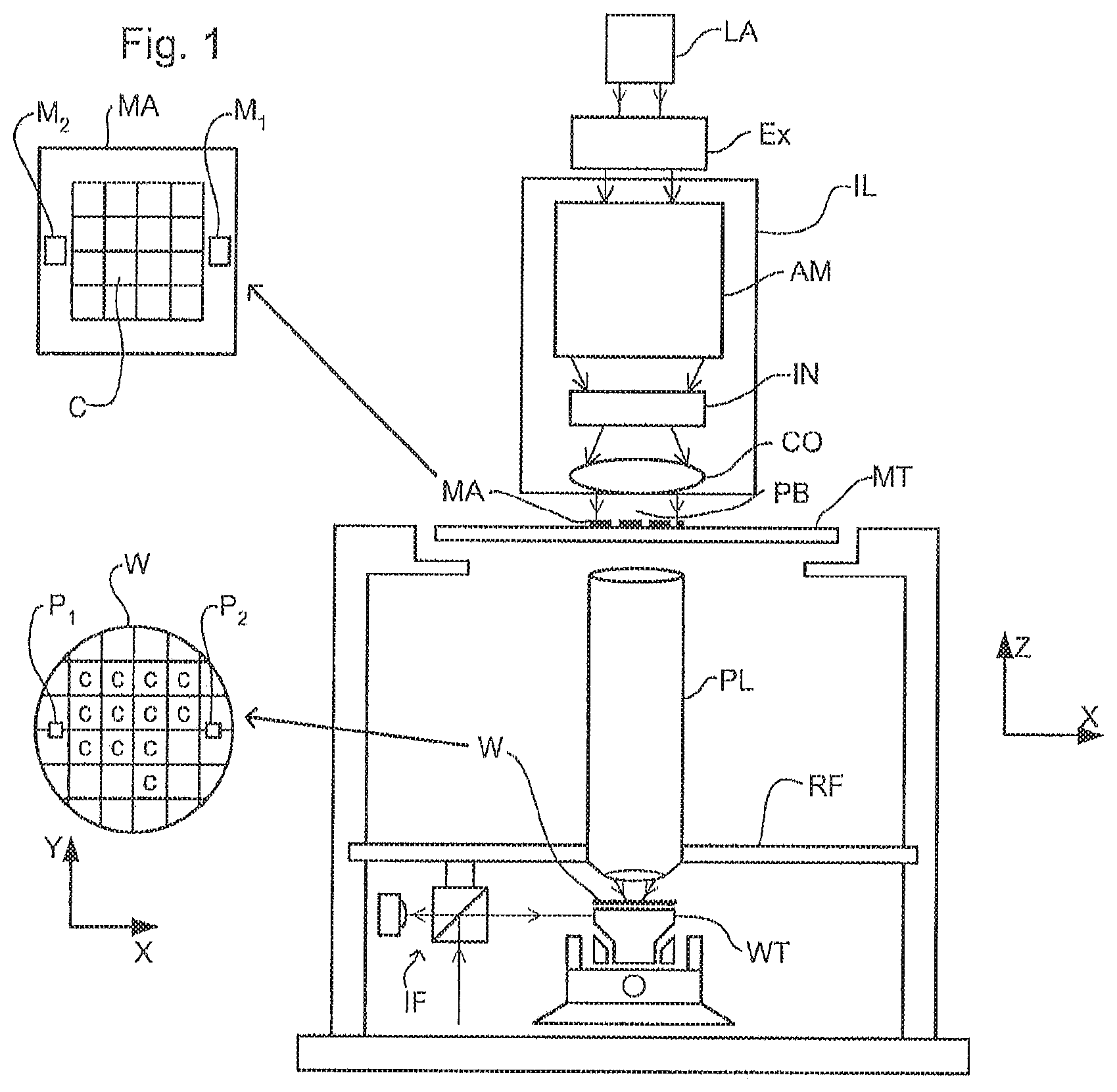
FIG. 1 schematically depicts a lithographic projection apparatus according to a particular embodiment of the invention. The apparatus comprises: a radiation system Ex, IL, for supplying a projection beam PB of radiation (e.g. DUV radiation), which in this particular case also comprises a radiation source LA; a first object table (mask table) MT provided with a mask holder for holding a mask MA (e.g. a reticle), and connected to a first positioning device for accurately positioning the mask with respect to item PL; a second object table (substrate table) WT provided with a substrate holder for holding a substrate W (e.g. a resist-coated silicon wafer), and connected to a second positioning device for accurately positioning the substrate with respect to item PL; a projection system ("projection lens") PL (e.g. a refractive system) for imaging an irradiated portion of the mask MA onto a target portion C (e.g. comprising one or more dies) of the substrate W.
As here depicted, the apparatus is of a transmissive type (e.g. has a transmissive mask). However, in general, it may also be of a reflective type, for example (e.g. with a reflective mask). Alternatively, the apparatus may employ another kind of patterning device, such as a programmable mirror array of a type as referred to above.
The source LA (e.g. an excimer laser) produces a beam of radiation. This beam is fed into an illumination system (illuminator) IL, either directly or after having traversed conditioning means, such as a beam expander Ex, for example. The illuminator IL may comprise adjusting means AM for setting the outer and/or inner radial extent (commonly referred to as .sigma.-outer and .sigma.-inner, respectively) of the intensity distribution in the beam. In addition, it will generally comprise various other components, such as an integrator IN and a condenser CO. In this way, the beam PB impinging on the mask MA has a desired uniformity and intensity distribution in its cross-section.
It should be noted with regard to FIG. 1 that the source LA may be within the housing of the lithographic projection apparatus (as is often the case when the source LA is a mercury lamp, for example), but that it may also be remote from the lithographic projection apparatus, the radiation beam which it produces being led into the apparatus (e.g. with the aid of suitable directing mirrors); this latter scenario is often the case when the source LA is an excimer laser. The current invention and claims encompass at least both of these scenarios.
The beam PB subsequently intercepts the mask MA, which is held on a mask table MT. Having traversed the mask MA, the beam PB passes through the projection system PL, which focuses the beam PB onto a target portion C of the substrate W. With the aid of the second positioning device (and interferometric measuring device IF), the substrate table WT can be moved accurately, e.g. so as to position different target portions C in the path of the beam PB. Similarly, the first positioning device can be used to accurately position the mask MA with respect to the path of the beam PB, e.g. after mechanical retrieval of the mask MA from a mask library, or during a scan. In general, movement of the object tables MT, WT will be realized with the aid of a long-stroke module (course positioning) and a short-stroke module (fine positioning), which are not explicitly depicted in FIG. 1. However, in the case of a stepper (as opposed to a step-and-scan apparatus) the mask table MT may just be connected to a short stroke actuator, or may be fixed.
The depicted apparatus can be used in two different modes:
1. In step mode, the mask table MT is kept essentially stationary, and an entire mask image is projected at one time (i.e. a single "flash") onto a target portion C. The substrate table WT is then shifted in the X and/or Y directions so that a different target portion C can be irradiated by the beam PB;
2. In scan mode, essentially the same scenario applies, except that a given target portion C is not exposed in a single "flash". Instead, the mask table MT is movable in a given direction (the so-called "scan direction", e.g. the Y direction) with a speed v, so that the projection beam PB is caused to scan over a mask image; concurrently, the substrate table WT is simultaneously moved in the same or opposite direction at a speed V=Mv, in which M is the magnification of the projection system PL (typically, M=1/4 or 1/5). In this manner, a relatively large target portion C can be exposed, without having to compromise on resolution.
FIG. 2 shows a liquid reservoir 10 between the projection system PL and the substrate W which is positioned on the substrate stage WT. The liquid reservoir 10 is filled with a liquid 11 having a relatively high refractive index, e.g. water or a suspension of particles in water, provided via inlet/outlet ducts 13. The liquid has the effect that the radiation of the projection beam is a shorter wavelength in the liquid than in gas (e.g., air) or in a vacuum, allowing smaller features to be resolved. It is well known that the resolution limit of a projection system is determined, inter alia, by the wavelength of the projection beam and the numerical aperture of the system. The presence of the liquid may also be regarded as increasing the effective numerical aperture. Furthermore, at fixed numerical aperture, the liquid is effective to increase the depth of field.
The reservoir 10 forms, in an embodiment, a contactless seal to the substrate W around the image field of the projection system PL so that the liquid is confined to fill the space between the substrate's primary surface, which faces the projection system PL, and the final optical element of the projection system PL. The reservoir is formed by a seal member 12 positioned below and surrounding the final element of the projection system PL. Thus, the liquid supply system provides liquid on only a localized area of the substrate. The seal member 12 forms part of the liquid supply system for filling the space between the final element of the projection system and the substrate with a liquid. This liquid is brought into the space below the projection system and within the seal member 12. In an embodiment, the seal member 12 extends a little above the bottom element of the projection system and the liquid rises above the final element so that a buffer of liquid is provided. The seal member 12 has an inner periphery that at the upper end closely conforms to the shape of the projection system or the final elements thereof and may, e.g. be round. At the bottom the inner periphery closely conforms to the shape of the image field, e.g. rectangular, though this is not necessarily so. The seal member is substantially stationary in the XY plane relative to the projection system though there may be some relative movement in the Z direction (in the direction of the optical axis). A seal is formed between the seal member and the surface of the substrate. In an implementation, this seal is a contactless seal and may be a gas seal.
The liquid 11 is confined in the reservoir 10 by a seal device 16. As illustrated in FIG. 2, the seal device is a contactless seal i.e. a gas seal. The gas seal is formed by gas, e.g. air or synthetic air, provided under pressure via inlet 15 to the gap between seal member 12 and substrate W and extracted by first outlet 14. The over pressure on the gas inlet 15, vacuum level or under pressure on the first outlet 14 and the geometry of the gap are arranged so that there is a high-velocity gas flow inwards towards the optical axis of the apparatus that confines the liquid 11. As with any seal, some liquid is likely to escape, for example up the first outlet 14.
FIGS. 14 and 15 also depict a liquid reservoir defined by inlet(s) IN, outlet(s) OUT, the substrate W and the final element of projection system PL. Like the liquid supply system of FIG. 2 the liquid supply system illustrated in FIGS. 14 and 15, comprising inlet(s) IN and outlet(s) OUT, supplies liquid to the primary surface of the substrate in a localized area between the final element of the projection system and the substrate and can suffer from loss of liquid at the substrate edge.
Thus, as used herein for the embodiments, the liquid supply system can comprise that as described in relation to FIG. 2 and FIGS. 14 and 15.
Embodiment 2
A second embodiment is illustrated in FIGS. 3 to 5 and is the same or similar as the first embodiment except as described below.
In the embodiment of FIGS. 3 and 4 an edge liquid supply system provides liquid to a reservoir 30 via a port 40. The liquid in the reservoir 30 is optionally the same as the immersion liquid in the liquid supply system. The reservoir 30 is positioned on the opposite side of the substrate W to the projection system PL and adjacent the edge of the substrate W and the edge of the edge seal member 17, 117. In FIG. 4, the edge seal member 17 is comprised of an element which is separate to the substrate table WT whereas in FIG. 3 the edge seal member 117 is provided by an integral portion of the substrate table WT. As can be seen most clearly from FIG. 3, the substrate W is supported on the substrate table WT by a so-called pimple table 20. The pimple table 20 comprises a plurality of projections on which the substrate W rests. The substrate W is held in place by, e.g., a vacuum source sucking the substrate onto the top surface of the substrate table WT. With the use of the reservoir 30, when the edge of the substrate W is being imaged, (i.e. when liquid in the liquid supply system between the projection system PL and the substrate W traverses across an edge of the substrate W), liquid cannot escape from the liquid supply system into the gap between the edge seal member 17, 117 and the substrate W because that space is already filled with liquid.
The mechanism 170 shown in FIG. 4 for moving the edge seal member 17 relative to the remainder of the substrate table WT is illustrated in detail in FIG. 5. The reason for moving the edge seal member 17 in this way is so that its primary surface can be made to be substantially co-planar with the primary surface of the substrate W. This allows a smooth movement of the liquid supply system over edge portions of the substrate W so that the bottom inner periphery of the liquid supply system can be moved to positions partly on the primary surface of substrate W and partly on the primary surface of the edge seal member 17.
A level sensor (not illustrated) is used to detect the relative heights of the primary surfaces of the substrate W and the edge seal member 17. Based on the results of the level sensor, control signals are sent to the actuator 171 in order to adjust the height of the primary surface of the edge seal member 17. A closed loop actuator could also be used for this purpose.
In an implementation, the actuator 171 is a rotating motor which rotates a shaft 176. The shaft 176 is connected to a circular disc at the end distal to the motor 171. The shaft 176 is connected away from the centre of the disc. The disc is located in a circular recess in a wedge portion 172. Ball bearings may be used to reduce the amount of friction between the circular disc and the sides of the recess in the wedge portion 172. The motor 171 is held in place by leaf springs 177. On actuation of the motor the wedge portion is driven to the left and right as illustrated (i.e. in the direction of the slope of the wedge portion) because of the excentre position of the shaft 176 in the disc. The motor is prevented from moving in the same direction as the direction of movement of the wedge portion 172 by the springs 177.
As the wedge portion 172 moves left and right as illustrated in FIG. 5, its top surface 175 (which is the surface of the wedge which is sloped in relation to the primary surface of the edge seal member 17) contacts the bottom sloped surface of a further wedge member 173 which is fixed to the bottom of the edge seal member 17. The edge seal member 17 is prevented from moving in the direction of movement of the wedge member 172 so that when the wedge member 172 moves left and right the edge seal member 17 is lowered and raised respectively. Some biasing of the edge seal member 17 towards the substrate table WT may be necessary.
Obviously the further wedge member 173 could be replaced by an alternative shape, for example a rod positioned perpendicularly to the direction of movement of the wedge 172. If the coefficient of friction between the wedge member 172 and the further wedge member 173 is greater than the tangent of the wedge angle then the actuator 170 is self-braking meaning that no force may be needed on the wedge member 172 to hold it in place. This is advantageous as the system will then be stable when the actuator 171 is not actuated. The accuracy of the mechanism 170 is of the order of a few .mu.m.
Especially in the case of the edge seal member 117 being an integral part of the substrate table WT, a mechanism may be provided to adjust the height of the substrate W or the member supporting the substrate W so that the primary surfaces of the edge seal member 17, 117 and the substrate can be made substantially co-planar.
Embodiment 3
A third embodiment is illustrated in FIGS. 6 and 7 and is the same or similar as the first embodiment except as described below.
This embodiment is described in relation to an edge seal member 117 which is an integral part of the substrate table WT. However, this embodiment is equally applicable to an edge seal member 17 which is movable relative to the substrate table WT.
In a first version of this embodiment as illustrated in FIG. 6a, a further edge seal member 500 is used to bridge the gap between the edge seal member 117 and the substrate W. The further edge seal member is affixed to the edge seal member 117. The further edge seal member 500 is removably attachable against the surface of the substrate W opposite the primary surface. In this embodiment the further edge seal member 500 can be a flexible edge seal member which is actuatable to contact the under surface of the substrate W. When the flexible edge seal member 500 is deactivated it falls away from the substrate under gravity. The way this is achieved is illustrated in FIG. 7 and is described below.
It is likely that the further edge seal member 500 will not prevent all of the immersion liquid from the liquid supply system from entering the space under the substrate W and for this reason a port 46 connected to a low pressure source may be provided under the substrate W adjacent edges of the edge seal member 117 and the substrate W in some or all of the versions of this embodiment. Of course the design of the area under the substrate could be the same as that of the second embodiment.
The same system can be used for sensors such as a transmission image sensor (TIS) on the substrate table as opposed for the substrate W. In the case of sensors, as the sensors do not move, the further edge seal member 500 can be permanently attached to the sensor, for example using glue.
Furthermore, the further edge seal member 500 can be arranged to engage with the top surface of the object (that surface closest to the projection system) rather than the bottom surface. Also, the further edge seal member 500 may be provided attached to or near the top surface of the edge seal member 117 as opposed to under the edge seal member 117 as is illustrated in FIG. 6a.
A second version of this embodiment is illustrated in FIG. 6b. Two further edge seal members 500a, 500b are used. The first of these edge seal members 500a is the same as in the first version. The second of these edge seal members 500b is affixed to the substrate table 20 i.e. underneath the substrate W and extends with its free end radially outwardly from its attachment point. The second further edge seal member 500b clamps the first further edge seal member 500a against the substrate W. Compressed gas can be used to deform or move the second further edge seal member 500b.
A third version of this embodiment is shown in FIG. 6c. The third version is the same as the second version except the first further edge seal member 500c clamps the second fu
D00000
D00001
D00002
D00003
D00004
D00005
D00006
D00007
D00008
D00009
D00010
XML
uspto.report is an independent third-party trademark research tool that is not affiliated, endorsed, or sponsored by the United States Patent and Trademark Office (USPTO) or any other governmental organization. The information provided by uspto.report is based on publicly available data at the time of writing and is intended for informational purposes only.
While we strive to provide accurate and up-to-date information, we do not guarantee the accuracy, completeness, reliability, or suitability of the information displayed on this site. The use of this site is at your own risk. Any reliance you place on such information is therefore strictly at your own risk.
All official trademark data, including owner information, should be verified by visiting the official USPTO website at www.uspto.gov. This site is not intended to replace professional legal advice and should not be used as a substitute for consulting with a legal professional who is knowledgeable about trademark law.