Elastic membrane for semiconductor wafer polishing
Yamaki , et al. Ja
U.S. patent number D839,224 [Application Number D/606,998] was granted by the patent office on 2019-01-29 for elastic membrane for semiconductor wafer polishing. This patent grant is currently assigned to EBARA CORPORATION. The grantee listed for this patent is EBARA CORPORATION. Invention is credited to Makoto Fukushima, Masahiko Kishimoto, Osamu Nabeya, Keisuke Namiki, Tomoko Owada, Shingo Togashi, Satoru Yamaki.


| United States Patent | D839,224 |
| Yamaki , et al. | January 29, 2019 |
Elastic membrane for semiconductor wafer polishing
Claims
CLAIM The ornamental design for an elastic membrane for semiconductor wafer polishing, as shown and described.
| Inventors: | Yamaki; Satoru (Tokyo, JP), Fukushima; Makoto (Tokyo, JP), Namiki; Keisuke (Tokyo, JP), Nabeya; Osamu (Tokyo, JP), Togashi; Shingo (Tokyo, JP), Owada; Tomoko (Tokyo, JP), Kishimoto; Masahiko (Tokyo, JP) | ||||||||||
|---|---|---|---|---|---|---|---|---|---|---|---|
| Applicant: |
|
||||||||||
| Assignee: | EBARA CORPORATION (Tokyo,
JP) |
||||||||||
| Appl. No.: | D/606,998 | ||||||||||
| Filed: | June 9, 2017 |
Foreign Application Priority Data
| Dec 12, 2016 [JP] | 2016-026913 | |||
| Dec 12, 2016 [JP] | 2016-026914 | |||
| Dec 12, 2016 [JP] | 2016-026915 | |||
| Current U.S. Class: | D13/182 |
| Current International Class: | 1303 |
| Field of Search: | ;D13/182 ;451/66,288,289 |
References Cited [Referenced By]
U.S. Patent Documents
| D363464 | October 1995 | Fukasawa |
| D411516 | June 1999 | Imafuku et al. |
| 6659850 | December 2003 | Korovin |
| D546784 | July 2007 | Hayashi |
| D553104 | October 2007 | Oohashi et al. |
| D557226 | December 2007 | Uchino |
| D559993 | January 2008 | Nagakubo |
| D559994 | January 2008 | Nagakubo |
| D633452 | March 2011 | Namiki |
| D634719 | March 2011 | Yasuda |
| D649126 | November 2011 | Takahashi |
| 8469776 | June 2013 | Zuniga |
| D709536 | July 2014 | Yoshimura |
| D709538 | July 2014 | Mizukami |
| D709539 | July 2014 | Kuwabara |
| D711330 | August 2014 | Fukushima |
| 8859070 | October 2014 | Yasuda |
| D729753 | May 2015 | Fukushima |
| 9376752 | June 2016 | Goel |
| D767234 | September 2016 | Kirkland |
| D769200 | October 2016 | Fukushima et al. |
| D770990 | November 2016 | Fukushima et al. |
| D770992 | November 2016 | Tauchi |
| D783922 | April 2017 | Kirkland |
| D797067 | September 2017 | Zhang |
| D808349 | January 2018 | Fukushima |
| D810705 | February 2018 | Krishnan |
| 2009/0247057 | October 2009 | Kobayashi |
| 2013/0316628 | November 2013 | Jang |
| 2014/0262193 | September 2014 | Im |
| 2016/0002788 | January 2016 | Nal |
| 2017/0009367 | January 2017 | Harris |
Attorney, Agent or Firm: Pearne & Gordon LLP
Description
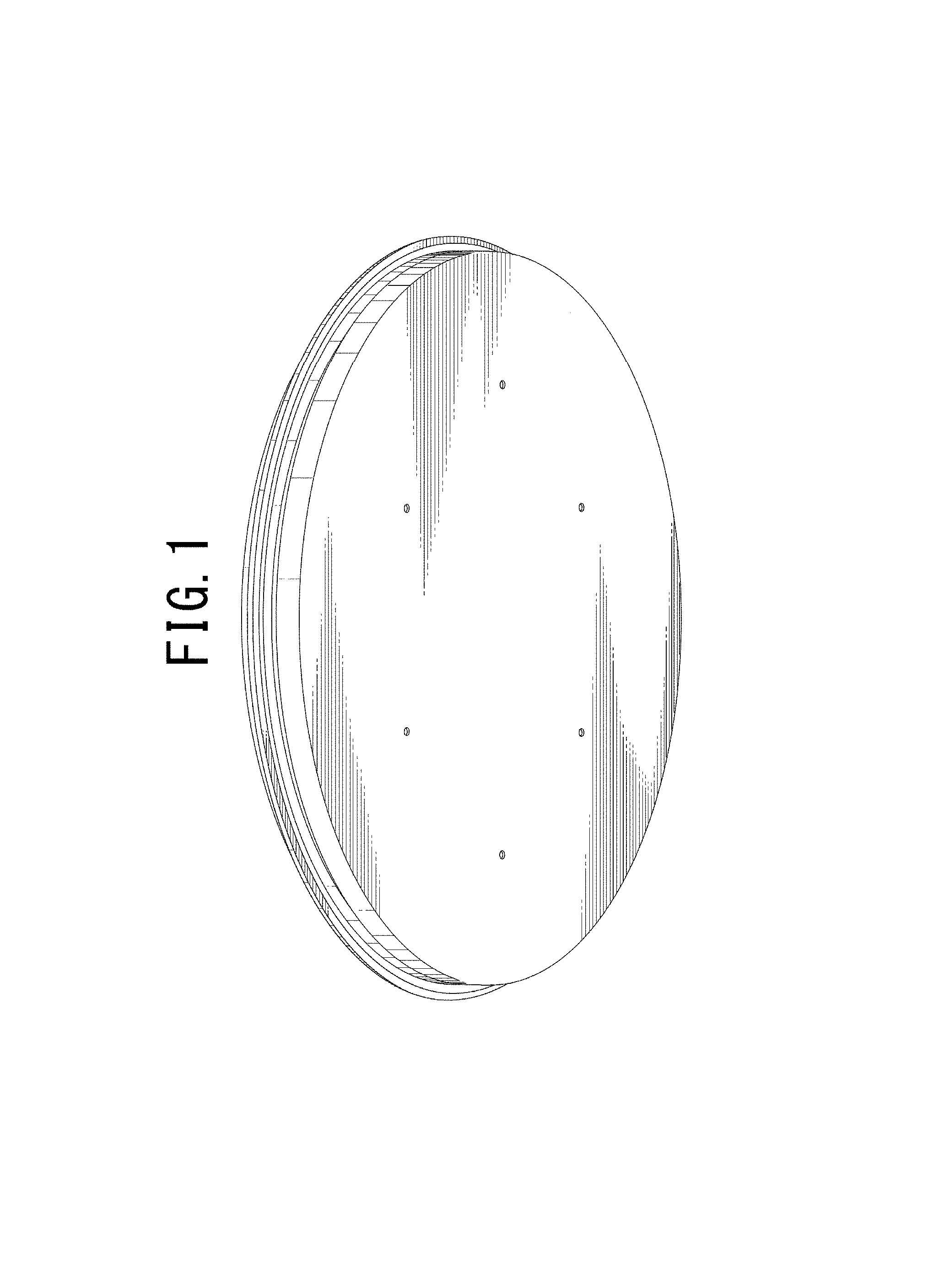
FIG. 1 is a bottom perspective view of an elastic membrane for semiconductor wafer polishing showing our new design;
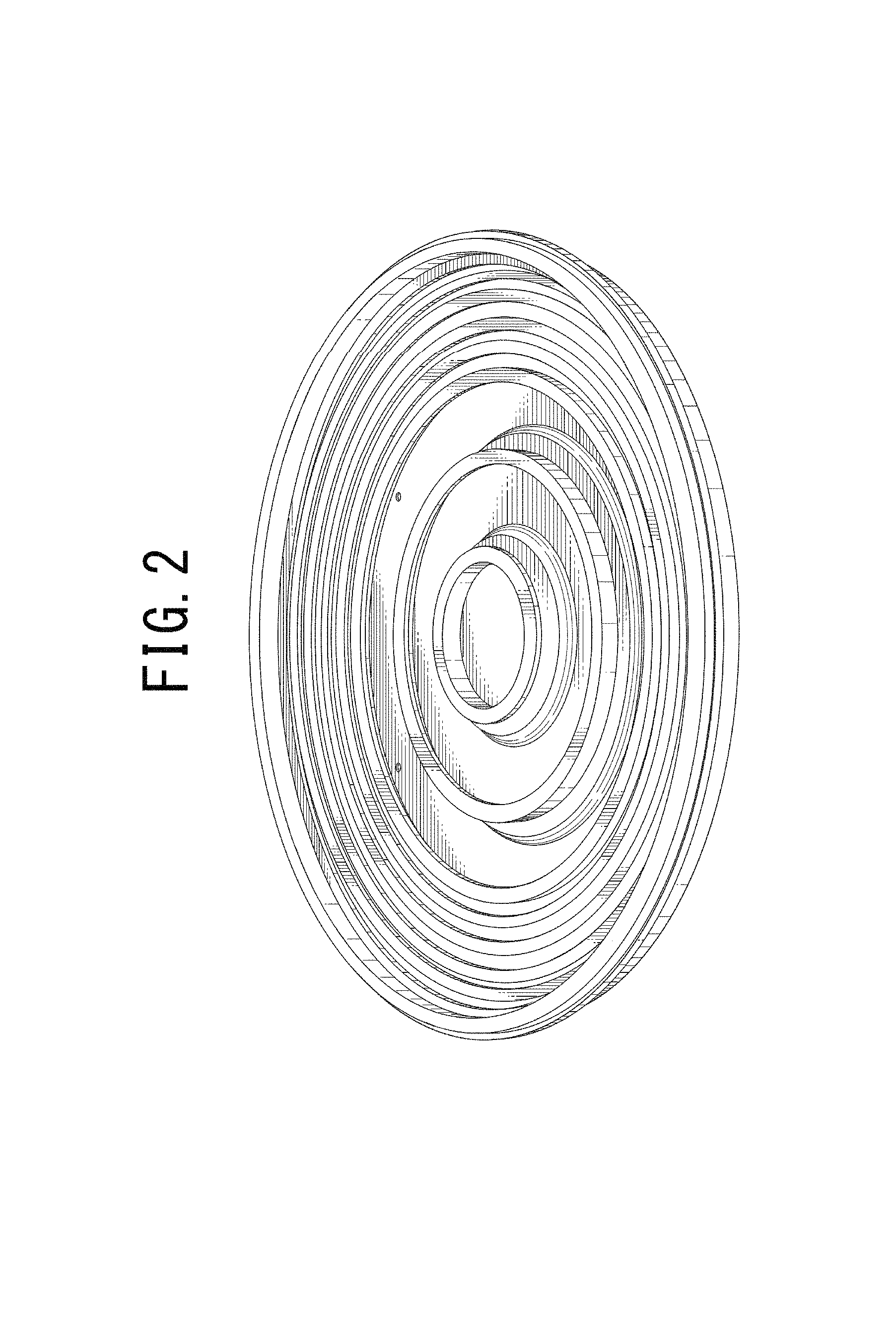
FIG. 2 is a top perspective view thereof;
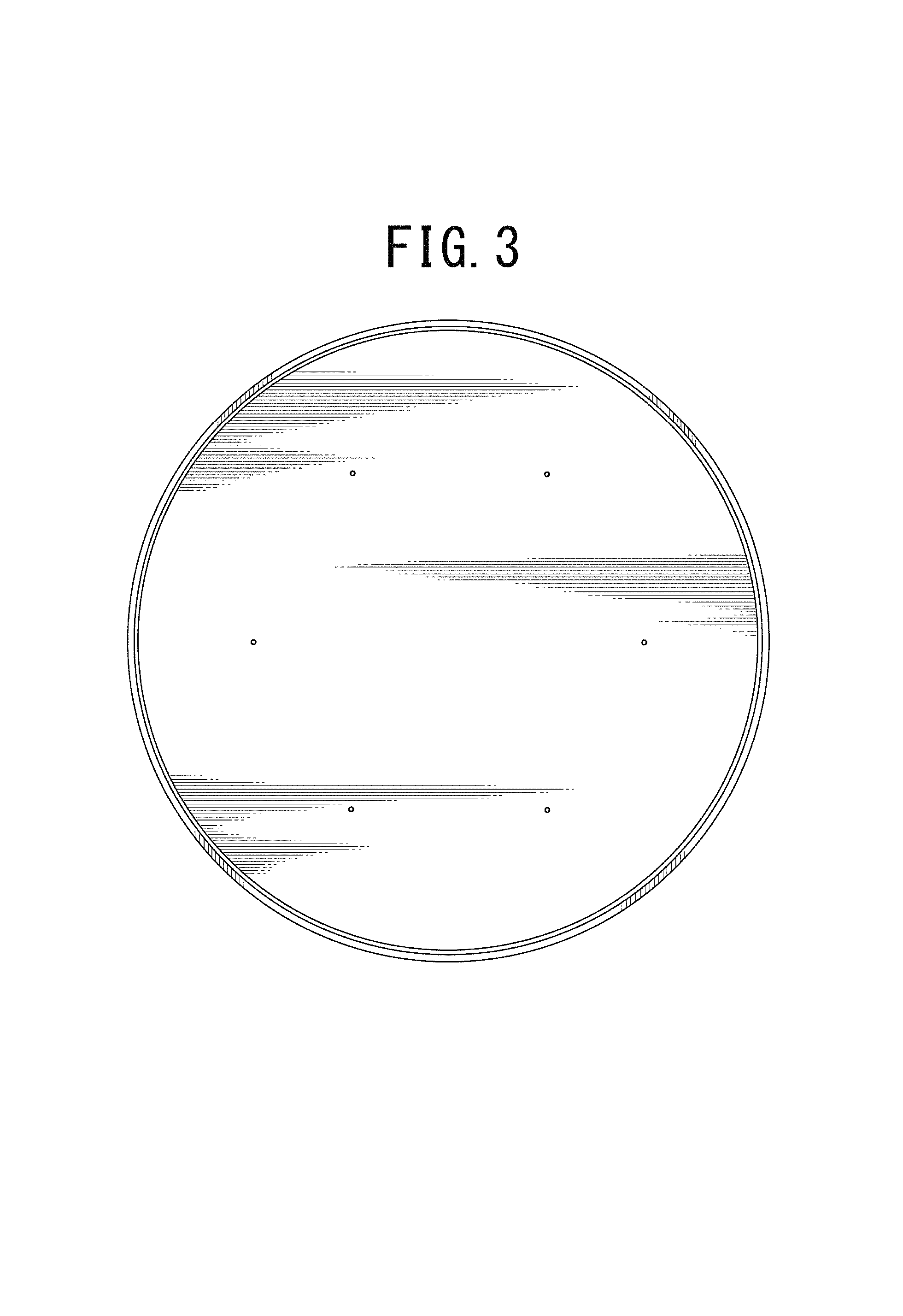
FIG. 3 is a bottom view thereof;
FIG. 4 is a top view thereof;
FIG. 5 is a front view thereof, a rear view being identical thereto;
FIG. 6 is a right-side view thereof, a left-side view being identical thereto;
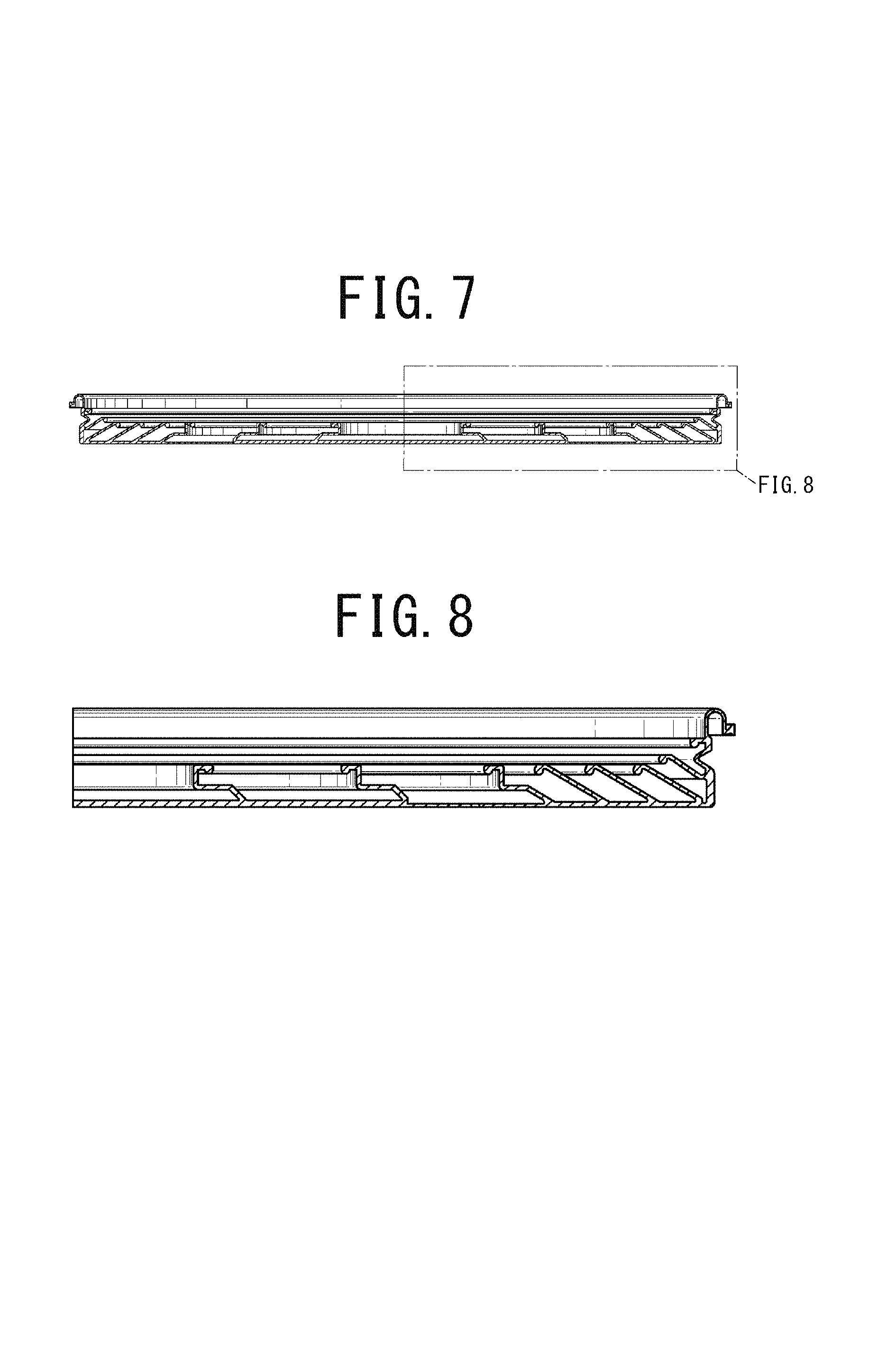
FIG. 7 is a cross-sectional view taken along line 7-7 of FIG. 4; and,
FIG. 8 is an enlarged portion view labeled FIG. 8 in FIG. 7.
The dash-dot lines in FIG. 7 represent the boundary line of the enlarged portion view shown in FIG. 8.
* * * * *
D00000
D00001
D00002
D00003
D00004
D00005
D00006
XML
uspto.report is an independent third-party trademark research tool that is not affiliated, endorsed, or sponsored by the United States Patent and Trademark Office (USPTO) or any other governmental organization. The information provided by uspto.report is based on publicly available data at the time of writing and is intended for informational purposes only.
While we strive to provide accurate and up-to-date information, we do not guarantee the accuracy, completeness, reliability, or suitability of the information displayed on this site. The use of this site is at your own risk. Any reliance you place on such information is therefore strictly at your own risk.
All official trademark data, including owner information, should be verified by visiting the official USPTO website at www.uspto.gov. This site is not intended to replace professional legal advice and should not be used as a substitute for consulting with a legal professional who is knowledgeable about trademark law.