Systems and methods utilizing solid-phase etchants
Chen , et al. December 22, 2
U.S. patent number 10,872,778 [Application Number 16/028,928] was granted by the patent office on 2020-12-22 for systems and methods utilizing solid-phase etchants. This patent grant is currently assigned to Applied Materials, Inc.. The grantee listed for this patent is Applied Materials, Inc.. Invention is credited to Zhijun Chen, Nitin Ingle, Chia-Ling Kao, Anchuan Wang.


| United States Patent | 10,872,778 |
| Chen , et al. | December 22, 2020 |
Systems and methods utilizing solid-phase etchants
Abstract
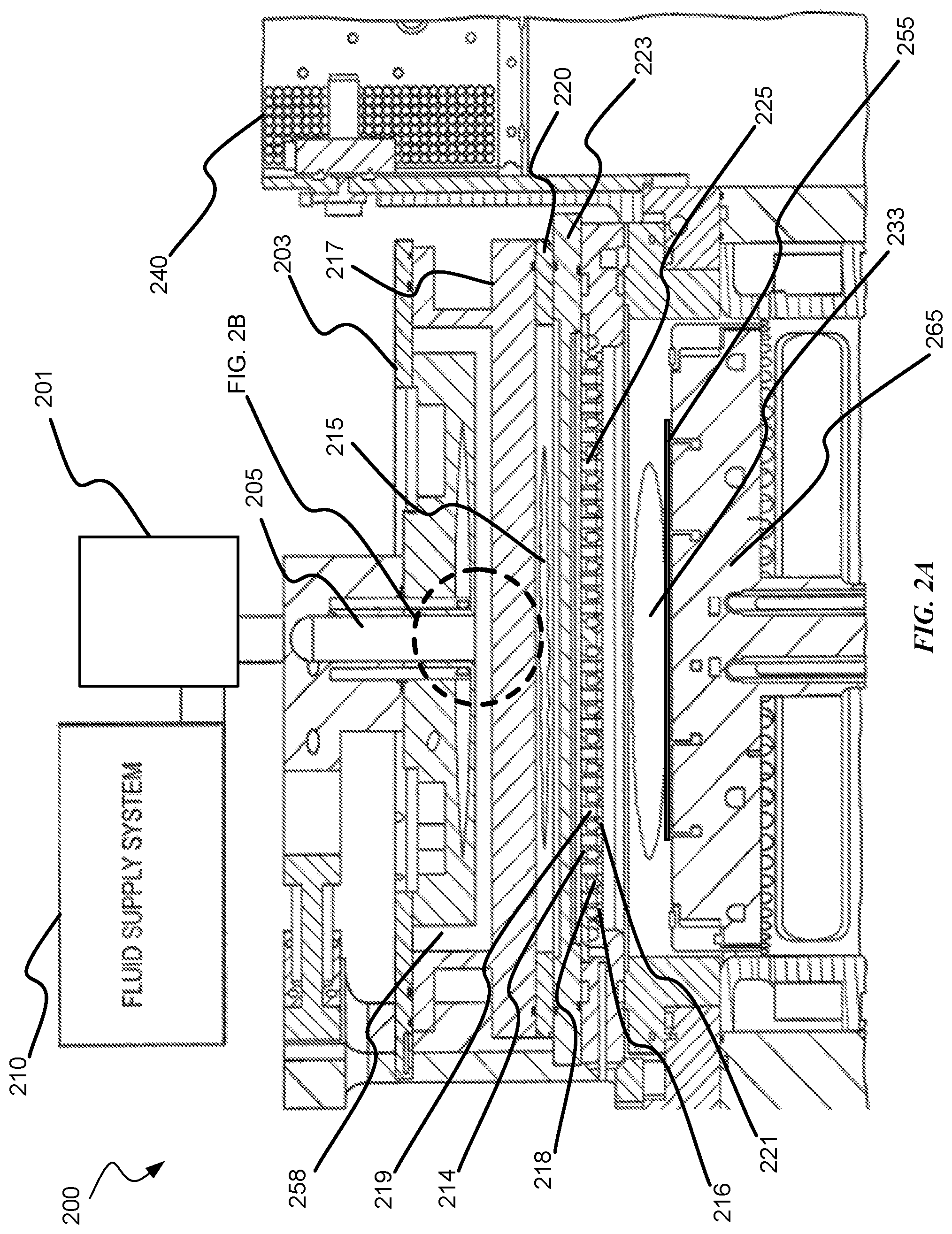
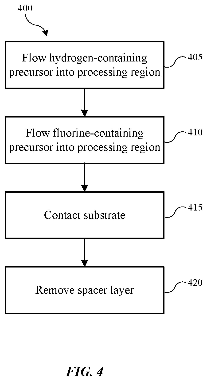
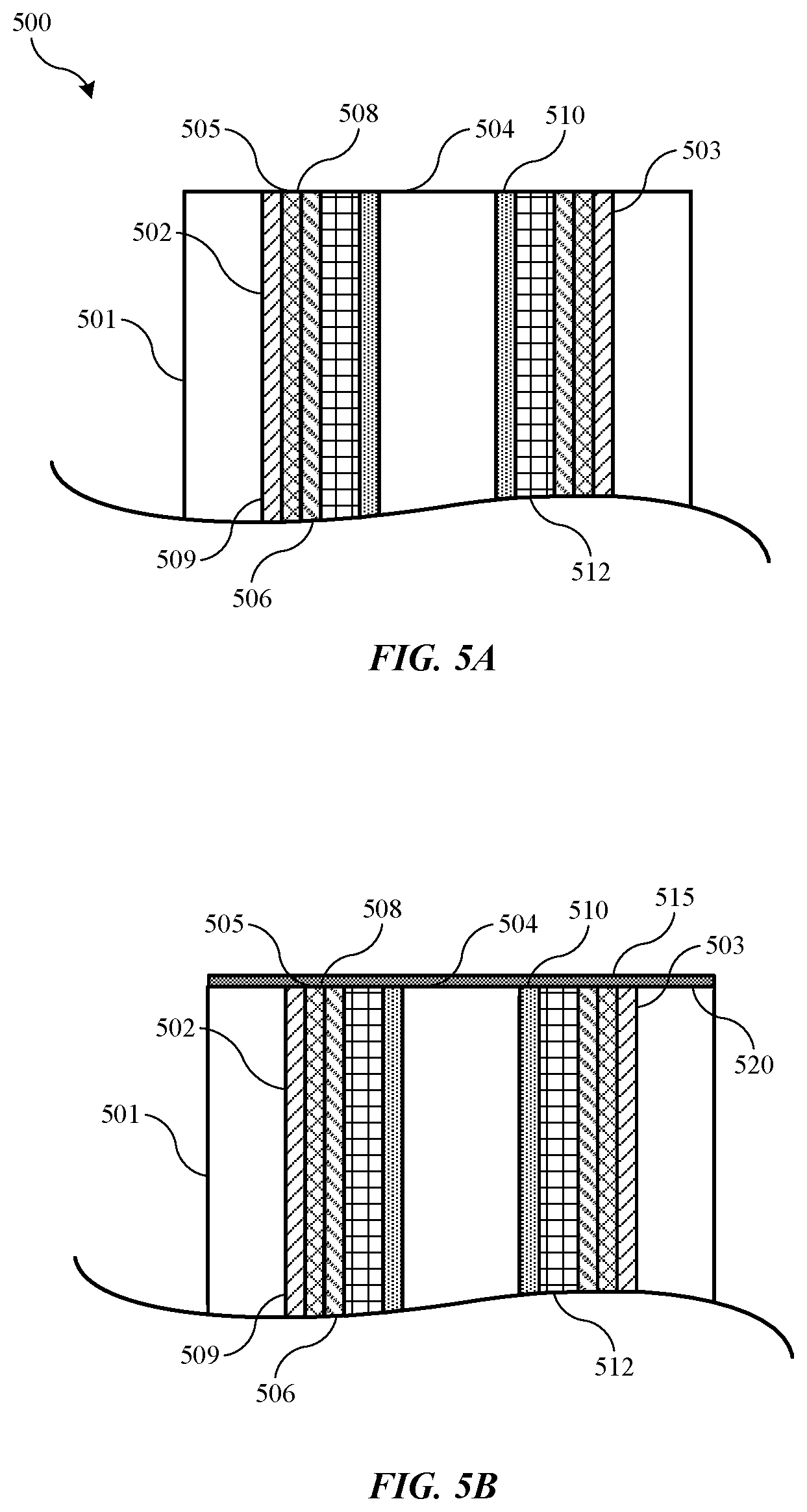
Exemplary etching methods may include flowing a hydrogen-containing precursor into a substrate processing region of a semiconductor processing chamber. The methods may include flowing a fluorine-containing precursor into the substrate processing region. The methods may include contacting a substrate housed in the substrate processing region with the hydrogen-containing precursor and the fluorine-containing precursor. The substrate may define a trench. A spacer may be formed along a sidewall of the trench, and the spacer may include a plurality of layers including a first layer of a carbon-containing material, a second layer of an oxygen-containing material, and a third layer of a carbon-containing material. The second layer of the spacer may be disposed between the first layer and third layer of the spacer. The methods may also include removing the oxygen-containing material.
| Inventors: | Chen; Zhijun (San Jose, CA), Kao; Chia-Ling (San Jose, CA), Wang; Anchuan (San Jose, CA), Ingle; Nitin (San Jose, CA) | ||||||||||
|---|---|---|---|---|---|---|---|---|---|---|---|
| Applicant: |
|
||||||||||
| Assignee: | Applied Materials, Inc. (Santa
Clara, CA) |
||||||||||
| Family ID: | 1000005258215 | ||||||||||
| Appl. No.: | 16/028,928 | ||||||||||
| Filed: | July 6, 2018 |
Prior Publication Data
| Document Identifier | Publication Date | |
|---|---|---|
| US 20200013632 A1 | Jan 9, 2020 | |
| Current U.S. Class: | 1/1 |
| Current CPC Class: | H01L 21/31105 (20130101); H01L 21/02164 (20130101); H01L 21/67063 (20130101); H01L 21/311 (20130101); H01L 21/7682 (20130101) |
| Current International Class: | H01L 21/768 (20060101); H01L 21/02 (20060101); C23C 16/00 (20060101); H01L 21/311 (20060101); H01L 21/67 (20060101) |
References Cited [Referenced By]
U.S. Patent Documents
| 2369620 | February 1945 | Sullivan et al. |
| 3401302 | September 1968 | Thorpe |
| 3451840 | June 1969 | Hough |
| 3537474 | November 1970 | Rohrer |
| 3756511 | September 1973 | Shinroku |
| 3937857 | February 1976 | Brummett et al. |
| 3969077 | July 1976 | Hill |
| 4006047 | February 1977 | Brummett et al. |
| 4190488 | February 1980 | Winters |
| 4209357 | June 1980 | Gorin et al. |
| 4214946 | July 1980 | Forget et al. |
| 4232060 | November 1980 | Mallory, Jr. |
| 4234628 | November 1980 | DuRose |
| 4265943 | May 1981 | Goldstein et al. |
| 4340462 | July 1982 | Koch |
| 4341592 | July 1982 | Shortes et al. |
| 4361418 | November 1982 | Tscheppe |
| 4361441 | November 1982 | Tylko |
| 4364803 | December 1982 | Nidola et al. |
| 4368223 | January 1983 | Kobayashi et al. |
| 4374698 | February 1983 | Sanders et al. |
| 4397812 | August 1983 | Mallory, Jr. |
| 4468413 | August 1984 | Bachmann |
| 4503807 | March 1985 | Nakayama et al. |
| 4565601 | January 1986 | Kakehi et al. |
| 4579618 | April 1986 | Celestino et al. |
| 4585920 | April 1986 | Hoog et al. |
| 4600464 | July 1986 | Desliets et al. |
| 4610775 | September 1986 | Phifer |
| 4625678 | December 1986 | Shloya et al. |
| 4632857 | December 1986 | Mallory, Jr. |
| 4656052 | April 1987 | Satou et al. |
| 4656076 | April 1987 | Vetanen et al. |
| 4668335 | May 1987 | Mockler |
| 4690746 | September 1987 | McInerney et al. |
| 4715937 | December 1987 | Moslehi et al. |
| 4749440 | June 1988 | Blackwood et al. |
| 4753898 | June 1988 | Parrillo et al. |
| 4786360 | November 1988 | Cote et al. |
| 4792378 | December 1988 | Rose et al. |
| 4793897 | December 1988 | Dunfield et al. |
| 4807016 | February 1989 | Douglas |
| 4810520 | March 1989 | Wu |
| 4816638 | March 1989 | Ukai et al. |
| 4820377 | April 1989 | Davis et al. |
| 4828649 | May 1989 | Davis |
| 4857140 | August 1989 | Loewenstein |
| 4867841 | September 1989 | Loewenstein et al. |
| 4904621 | February 1990 | Loewenstein et al. |
| 4913929 | April 1990 | Moslehi et al. |
| 4919750 | April 1990 | Bausmith et al. |
| 4946903 | August 1990 | Gardella et al. |
| 4951601 | August 1990 | Maydan et al. |
| 4960488 | October 1990 | Law et al. |
| 4980018 | December 1990 | Mu et al. |
| 4981551 | January 1991 | Palmour |
| 4985372 | January 1991 | Narita et al. |
| 4987856 | January 1991 | Hey et al. |
| 4991542 | February 1991 | Kohmura et al. |
| 4992136 | February 1991 | Tachi et al. |
| 4993358 | February 1991 | Mahawili |
| 4994404 | February 1991 | Sheng et al. |
| 5000113 | March 1991 | Wang et al. |
| 5006192 | April 1991 | Deguchi |
| 5010842 | April 1991 | Oda et al. |
| 5013691 | May 1991 | Lory et al. |
| 5028565 | July 1991 | Chang |
| 5030319 | July 1991 | Nishino et al. |
| 5038713 | August 1991 | Kawakami et al. |
| 5045244 | September 1991 | Marlett |
| 5061838 | October 1991 | Lane et al. |
| 5069938 | December 1991 | Lorimer et al. |
| 5074456 | December 1991 | Degner et al. |
| 5083030 | January 1992 | Stavov |
| 5089441 | February 1992 | Moslehi |
| 5089442 | February 1992 | Olmer |
| 5147692 | September 1992 | Bengston |
| 5156881 | October 1992 | Okano et al. |
| 5180435 | January 1993 | Markunas et al. |
| 5186718 | February 1993 | Tepman et al. |
| 5188706 | February 1993 | Hori et al. |
| 5198034 | March 1993 | deBoer et al. |
| 5200016 | April 1993 | Namose |
| 5203911 | April 1993 | Sricharoenchalkit et al. |
| 5215787 | June 1993 | Homma |
| 5217559 | June 1993 | Moslehi et al. |
| 5221427 | June 1993 | Koinuma et al. |
| 5228501 | July 1993 | Tepman et al. |
| 5231690 | July 1993 | Soma et al. |
| 5235139 | August 1993 | Bengston et al. |
| 5238499 | August 1993 | van de Ven et al. |
| 5240497 | August 1993 | Shacham et al. |
| 5248371 | September 1993 | Maher et al. |
| 5248527 | September 1993 | Uchida et al. |
| 5252178 | October 1993 | Moslehi |
| 5266157 | November 1993 | Kadomura |
| 5269881 | December 1993 | Sekiya |
| 5270125 | December 1993 | America et al. |
| 5271972 | December 1993 | Kwok et al. |
| 5275977 | January 1994 | Otsubo et al. |
| 5277750 | January 1994 | Wolgang |
| 5279669 | January 1994 | Lee |
| 5279865 | January 1994 | Chebi et al. |
| 5288518 | February 1994 | Homma |
| 5290382 | March 1994 | Zarowin et al. |
| 5290383 | March 1994 | Koshimizu |
| 5292370 | March 1994 | Tsai et al. |
| 5292682 | March 1994 | Stevens et al. |
| 5300463 | April 1994 | Cathey et al. |
| 5302233 | April 1994 | Kim et al. |
| 5304250 | April 1994 | Sameshima et al. |
| 5306530 | April 1994 | Strongin et al. |
| 5314724 | May 1994 | Tsukune et al. |
| 5319247 | June 1994 | Matsuura |
| 5326427 | July 1994 | Jerbic |
| 5328558 | July 1994 | Kawamura et al. |
| 5328810 | July 1994 | Lowrey et al. |
| 5330578 | July 1994 | Sakama |
| 5334552 | August 1994 | Homma |
| 5345999 | September 1994 | Hosokawa |
| 5352636 | October 1994 | Beinglass |
| 5356478 | October 1994 | Chen et al. |
| 5362526 | November 1994 | Wang et al. |
| 5366585 | November 1994 | Robertson et al. |
| 5368897 | November 1994 | Kurihara et al. |
| 5378316 | January 1995 | Franke et al. |
| 5380560 | January 1995 | Kaja et al. |
| 5382311 | January 1995 | Ishikawa et al. |
| 5384284 | January 1995 | Doan et al. |
| 5385763 | January 1995 | Okano et al. |
| 5399237 | March 1995 | Keswick et al. |
| 5399529 | March 1995 | Homma |
| 5403434 | April 1995 | Moslehi |
| 5413670 | May 1995 | Langan et al. |
| 5413967 | May 1995 | Matsuda et al. |
| 5415890 | May 1995 | Kloiber et al. |
| 5416048 | May 1995 | Blalock et al. |
| 5420075 | May 1995 | Homma et al. |
| 5429995 | July 1995 | Nishiyama et al. |
| 5439553 | August 1995 | Grant et al. |
| 5451169 | September 1995 | Corbett, III et al. |
| 5451259 | September 1995 | Krogh |
| 5454170 | October 1995 | Cook |
| 5464499 | November 1995 | Moslehi |
| 5468342 | November 1995 | Nulty et al. |
| 5474589 | December 1995 | Ohga et al. |
| 5478403 | December 1995 | Shinigawa et al. |
| 5478462 | December 1995 | Walsh |
| 5483920 | January 1996 | Pryor |
| 5494494 | February 1996 | Mizuno et al. |
| 5500249 | March 1996 | Telford et al. |
| 5505816 | April 1996 | Barnes et al. |
| 5510216 | April 1996 | Calabrese et al. |
| 5516367 | May 1996 | Lei et al. |
| 5518962 | May 1996 | Murao |
| 5531835 | July 1996 | Fodor et al. |
| 5534070 | July 1996 | Okamura et al. |
| 5536360 | July 1996 | Nguyen et al. |
| 5549780 | August 1996 | Koinuma et al. |
| 5556521 | September 1996 | Ghanbari |
| 5558717 | September 1996 | Zhao et al. |
| 5560779 | October 1996 | Knowles et al. |
| 5563105 | October 1996 | Dobuzinsky et al. |
| 5567243 | October 1996 | Foster et al. |
| 5571576 | November 1996 | Qian et al. |
| 5575853 | November 1996 | Arami et al. |
| 5578130 | November 1996 | Hayashi et al. |
| 5578161 | November 1996 | Auda |
| 5580385 | December 1996 | Paranjpe et al. |
| 5580421 | December 1996 | Hiatt et al. |
| 5591269 | January 1997 | Arami et al. |
| 5592358 | January 1997 | Shamouilian |
| 5595606 | January 1997 | Fujikawa et al. |
| 5597439 | January 1997 | Salzman |
| 5599740 | February 1997 | Jang et al. |
| 5614055 | March 1997 | Fairbairn et al. |
| 5616518 | April 1997 | Foo et al. |
| 5624582 | April 1997 | Cain |
| 5626922 | May 1997 | Miyanaga et al. |
| 5628829 | May 1997 | Foster et al. |
| 5635086 | June 1997 | Warren, Jr. |
| 5645645 | July 1997 | Zhang et al. |
| 5648125 | July 1997 | Cane |
| 5648175 | July 1997 | Russell et al. |
| 5656093 | August 1997 | Burkhart et al. |
| 5660957 | August 1997 | Chou et al. |
| 5661093 | August 1997 | Ravi et al. |
| 5670066 | September 1997 | Barnes et al. |
| 5674787 | October 1997 | Zhao et al. |
| 5676758 | October 1997 | Hasgawa et al. |
| 5679606 | October 1997 | Wang et al. |
| 5685946 | November 1997 | Fathauer et al. |
| 5688331 | November 1997 | Aruga et al. |
| 5695810 | December 1997 | Dubin et al. |
| 5712185 | January 1998 | Tsai et al. |
| 5716500 | February 1998 | Bardos et al. |
| 5716506 | February 1998 | Maclay et al. |
| 5719085 | February 1998 | Moon et al. |
| 5733816 | March 1998 | Iyer et al. |
| 5747373 | May 1998 | Yu |
| 5753886 | May 1998 | Iwamura et al. |
| 5755859 | May 1998 | Brusic et al. |
| 5756400 | May 1998 | Ye et al. |
| 5756402 | May 1998 | Jimbo et al. |
| 5772770 | June 1998 | Suda et al. |
| 5781693 | July 1998 | Ballance et al. |
| 5786276 | July 1998 | Brooks et al. |
| 5788825 | August 1998 | Park et al. |
| 5789300 | August 1998 | Fulford |
| 5792376 | August 1998 | Kanai et al. |
| 5800686 | September 1998 | Littau et al. |
| 5804259 | September 1998 | Robles |
| 5812403 | September 1998 | Fong et al. |
| 5814238 | September 1998 | Ashby et al. |
| 5814365 | September 1998 | Mahawill |
| 5820723 | October 1998 | Benjamin et al. |
| 5824599 | October 1998 | Schacham-Diamand et al. |
| 5830805 | November 1998 | Schacham-Diamand et al. |
| 5835334 | November 1998 | McMillin et al. |
| 5843538 | December 1998 | Ehrsam et al. |
| 5843847 | December 1998 | Pu et al. |
| 5844195 | December 1998 | Fairbairn et al. |
| 5846332 | December 1998 | Zhao et al. |
| 5846373 | December 1998 | Pirkle et al. |
| 5846375 | December 1998 | Gilchrist et al. |
| 5846598 | December 1998 | Semkow et al. |
| 5849639 | December 1998 | Molloy et al. |
| 5850105 | December 1998 | Dawson et al. |
| 5855681 | January 1999 | Maydan et al. |
| 5855685 | January 1999 | Tobe et al. |
| 5856240 | January 1999 | Sinha et al. |
| 5858876 | January 1999 | Chew |
| 5863376 | January 1999 | Wicker |
| 5865896 | February 1999 | Nowak |
| 5866483 | February 1999 | Shiau et al. |
| 5868897 | February 1999 | Ohkawa |
| 5872052 | February 1999 | Iyer |
| 5872058 | February 1999 | Van Cleemput et al. |
| 5882424 | March 1999 | Taylor et al. |
| 5882786 | March 1999 | Nassau et al. |
| 5883012 | March 1999 | Chiou |
| 5885404 | March 1999 | Kim et al. |
| 5885749 | March 1999 | Huggins et al. |
| 5888906 | March 1999 | Sandhu et al. |
| 5891349 | April 1999 | Tobe et al. |
| 5891513 | April 1999 | Dubin et al. |
| 5897751 | April 1999 | Makowiecki |
| 5899752 | May 1999 | Hey et al. |
| 5900163 | May 1999 | Yi et al. |
| 5904827 | May 1999 | Reynolds |
| 5907790 | May 1999 | Kellam |
| 5910340 | June 1999 | Uchida et al. |
| 5913147 | June 1999 | Dubin et al. |
| 5913978 | June 1999 | Kato et al. |
| 5915190 | June 1999 | Pirkle |
| 5918116 | June 1999 | Chittipeddi |
| 5919332 | July 1999 | Koshiishi et al. |
| 5920792 | July 1999 | Lin |
| 5926737 | July 1999 | Ameen et al. |
| 5928528 | July 1999 | Kubota et al. |
| 5932077 | August 1999 | Reynolds |
| 5933757 | August 1999 | Yoshikawa et al. |
| 5935334 | August 1999 | Fong et al. |
| 5935340 | August 1999 | Xia et al. |
| 5937323 | August 1999 | Orczyk et al. |
| 5939831 | August 1999 | Fong et al. |
| 5942075 | August 1999 | Nagahata et al. |
| 5944049 | August 1999 | Beyer et al. |
| 5944902 | August 1999 | Redeker et al. |
| 5948702 | September 1999 | Rotondaro |
| 5951601 | September 1999 | Lesinski et al. |
| 5951776 | September 1999 | Selyutin et al. |
| 5951896 | September 1999 | Mahawill |
| 5953591 | September 1999 | Ishihara et al. |
| 5953635 | September 1999 | Andideh |
| 5963840 | October 1999 | Xia et al. |
| 5968379 | October 1999 | Zhao et al. |
| 5968587 | October 1999 | Frankel et al. |
| 5968610 | October 1999 | Liu et al. |
| 5969422 | October 1999 | Ting et al. |
| 5976327 | November 1999 | Tanaka |
| 5982100 | November 1999 | Ghanbari |
| 5990000 | November 1999 | Hong et al. |
| 5990013 | November 1999 | Berenguer et al. |
| 5993916 | November 1999 | Zhao et al. |
| 5994209 | November 1999 | Yieh et al. |
| 5997649 | December 1999 | Hillman |
| 5997721 | December 1999 | Limbach et al. |
| 5997962 | December 1999 | Ogasawara et al. |
| 6004884 | December 1999 | Abraham |
| 6007635 | December 1999 | Mahawill |
| 6007785 | December 1999 | Liou |
| 6010962 | January 2000 | Liu et al. |
| 6013191 | January 2000 | Nasser-Faili et al. |
| 6013584 | January 2000 | M'Saad |
| 6015724 | January 2000 | Yamazaki et a |
| 6015747 | January 2000 | Lopatin et al. |
| 6017414 | January 2000 | Koemtzopoulos et al. |
| 6019848 | February 2000 | Kiyama et al. |
| 6020271 | February 2000 | Yanagida |
| 6030666 | February 2000 | Lam et al. |
| 6030881 | February 2000 | Papasouliotis et al. |
| 6035101 | March 2000 | Sajoto et al. |
| 6036878 | March 2000 | Collins et al. |
| 6037018 | March 2000 | Jang et al. |
| 6037266 | March 2000 | Tao et al. |
| 6039834 | March 2000 | Tanaka et al. |
| 6039851 | March 2000 | Iyer |
| 6053982 | April 2000 | Halpin et al. |
| 6059643 | May 2000 | Hu et al. |
| 6063683 | May 2000 | Wu et al. |
| 6063712 | May 2000 | Gilton et al. |
| 6065424 | May 2000 | Shacham-Diamand et al. |
| 6065425 | May 2000 | Takaki et al. |
| 6072147 | June 2000 | Koshiishi |
| 6072227 | June 2000 | Yau et al. |
| 6074512 | June 2000 | Collins et al. |
| 6074514 | June 2000 | Bjorkman et al. |
| 6077384 | June 2000 | Collins et al. |
| 6077386 | June 2000 | Smith, Jr. et al. |
| 6077780 | June 2000 | Dubin |
| 6079356 | June 2000 | Umotoy et al. |
| 6080529 | June 2000 | Ye et al. |
| 6081414 | June 2000 | Flanigan et al. |
| 6083344 | July 2000 | Hanawa et al. |
| 6083844 | July 2000 | Bui-Le et al. |
| 6086677 | July 2000 | Umotoy et al. |
| 6087278 | July 2000 | Kim et al. |
| 6090212 | July 2000 | Mahawill |
| 6093457 | July 2000 | Okumura |
| 6093594 | July 2000 | Yeap et al. |
| 6099697 | August 2000 | Hausmann |
| 6107199 | August 2000 | Allen et al. |
| 6110530 | August 2000 | Chen et al. |
| 6110832 | August 2000 | Morgan et al. |
| 6110836 | August 2000 | Cohen et al. |
| 6110838 | August 2000 | Loewenstein |
| 6113771 | September 2000 | Landau et al. |
| 6114216 | September 2000 | Yieh et al. |
| 6117245 | September 2000 | Mandrekar et al. |
| 6120640 | September 2000 | Shih et al. |
| 6124003 | September 2000 | Mikami et al. |
| 6126753 | October 2000 | Shinriki et al. |
| 6132512 | October 2000 | Horie et al. |
| 6136163 | October 2000 | Cheung et al. |
| 6136165 | October 2000 | Moslehi et al. |
| 6136685 | October 2000 | Narwankar et al. |
| 6136693 | October 2000 | Chan et al. |
| 6140234 | October 2000 | Uzoh et al. |
| 6144099 | November 2000 | Lopatin et al. |
| 6147009 | November 2000 | Grill et al. |
| 6148761 | November 2000 | Majewski et al. |
| 6149828 | November 2000 | Vaartstra |
| 6150628 | November 2000 | Smith et al. |
| 6153935 | November 2000 | Edelstein et al. |
| 6161500 | December 2000 | Kopacz et al. |
| 6161576 | December 2000 | Maher et al. |
| 6162302 | December 2000 | Raghavan et al. |
| 6162370 | December 2000 | Hackett et al. |
| 6165912 | December 2000 | McConnell et al. |
| 6167834 | January 2001 | Wang et al. |
| 6169021 | January 2001 | Akram et al. |
| 6170428 | January 2001 | Redeker et al. |
| 6170429 | January 2001 | Schoepp |
| 6171661 | January 2001 | Zheng et al. |
| 6174450 | January 2001 | Patrick et al. |
| 6174810 | January 2001 | Patrick et al. |
| 6174812 | January 2001 | Hsuing et al. |
| 6176198 | January 2001 | Kao et al. |
| 6176667 | January 2001 | Fairbairn |
| 6177245 | January 2001 | Ward et al. |
| 6179924 | January 2001 | Zhao et al. |
| 6180523 | January 2001 | Lee et al. |
| 6182602 | February 2001 | Redeker et al. |
| 6182603 | February 2001 | Shang et al. |
| 6184121 | February 2001 | Buchwalter et al. |
| 6184489 | February 2001 | Ito et al. |
| 6186091 | February 2001 | Chu et al. |
| 6189483 | February 2001 | Ishikawa et al. |
| 6190233 | February 2001 | Hong et al. |
| 6194038 | February 2001 | Rossman |
| 6197181 | March 2001 | Chen |
| 6197364 | March 2001 | Paunovic et al. |
| 6197680 | March 2001 | Lin et al. |
| 6197688 | March 2001 | Simpson |
| 6197705 | March 2001 | Vassiliev |
| 6198616 | March 2001 | Dahimene et al. |
| 6200412 | March 2001 | Kilgore et al. |
| 6203863 | March 2001 | Liu et al. |
| 6204200 | March 2001 | Shieh et al. |
| 6210486 | April 2001 | Mizukami et al. |
| 6217658 | April 2001 | Orczyk et al. |
| 6220201 | April 2001 | Nowak |
| 6225745 | May 2001 | Srivastava |
| 6228233 | May 2001 | Lakshmikanthan et al. |
| 6228751 | May 2001 | Yamazaki et al. |
| 6228758 | May 2001 | Pellerin et al. |
| 6235643 | May 2001 | Mui et al. |
| 6237527 | May 2001 | Kellerman et al. |
| 6238513 | May 2001 | Arnold et al. |
| 6238582 | May 2001 | Williams et al. |
| 6197151 | June 2001 | Kaji et al. |
| 6241845 | June 2001 | Gadgil et al. |
| 6242349 | June 2001 | Nogami et al. |
| 6242360 | June 2001 | Fischer et al. |
| 6244211 | June 2001 | Nishikawa et al. |
| 6245396 | June 2001 | Nogami |
| 6245670 | June 2001 | Cheung et al. |
| 6251236 | June 2001 | Stevens |
| 6251802 | June 2001 | Moore et al. |
| 6258170 | July 2001 | Somekh et al. |
| 6258220 | July 2001 | Dordi et al. |
| 6258223 | July 2001 | Cheung et al. |
| 6258270 | July 2001 | Hilgendorff et al. |
| 6261637 | July 2001 | Oberle |
| 6267074 | July 2001 | Okumura |
| 6277733 | August 2001 | Smith |
| 6277752 | August 2001 | Chen |
| 6277763 | August 2001 | Kugimiya et al. |
| 6281072 | August 2001 | Li et al. |
| 6281135 | August 2001 | Han et al. |
| 6284146 | September 2001 | Kim et al. |
| 6291282 | September 2001 | Wilk et al. |
| 6291348 | September 2001 | Lopatin et al. |
| 6302964 | October 2001 | Umotoy et al. |
| 6303044 | October 2001 | Koemtzopoulos et al. |
| 6303418 | October 2001 | Cha et al. |
| 6306246 | October 2001 | Melvin et al. |
| 6306772 | October 2001 | Lin |
| 6308654 | October 2001 | Schneider et al. |
| 6308776 | October 2001 | Sloan |
| 6310755 | October 2001 | Busato et al. |
| 6312554 | November 2001 | Ye |
| 6312995 | November 2001 | Yu |
| 6319387 | November 2001 | Krishnamoorthy et al. |
| 6321587 | November 2001 | Laush |
| 6322716 | November 2001 | Qiao et al. |
| 6323128 | November 2001 | Sambucetti et al. |
| 6335288 | January 2002 | Kwan et al. |
| 6340435 | January 2002 | Bjorkman et al. |
| 6342733 | January 2002 | Hu et al. |
| RE37546 | February 2002 | Mahawill |
| 6344410 | February 2002 | Lopatin et al. |
| 6348407 | February 2002 | Gupta et al. |
| 6350320 | February 2002 | Sherstinsky et al. |
| 6350697 | February 2002 | Richardson |
| 6351013 | February 2002 | Luning et al. |
| 6352081 | March 2002 | Lu et al. |
| 6355573 | March 2002 | Okumura |
| 6358827 | March 2002 | Chen et al. |
| 6364949 | April 2002 | Or et al. |
| 6364954 | April 2002 | Umotoy et al. |
| 6364957 | April 2002 | Schneider et al. |
| 6375748 | April 2002 | Yudovsky et al. |
| 6376386 | April 2002 | Oshima |
| 6379575 | April 2002 | Yin et al. |
| 6383896 | May 2002 | Kirimura et al. |
| 6383951 | May 2002 | Li |
| 6387207 | May 2002 | Janakiraman et al. |
| 6391753 | May 2002 | Yu |
| 6395150 | May 2002 | Van Cleemput et al. |
| 6403491 | June 2002 | Liu et al. |
| 6415736 | July 2002 | Hao et al. |
| 6416647 | July 2002 | Dordi et al. |
| 6418874 | July 2002 | Cox et al. |
| 6423284 | July 2002 | Arno |
| 6427623 | August 2002 | Ko |
| 6429465 | August 2002 | Yagi et al. |
| 6432819 | August 2002 | Pavate et al. |
| 6432831 | August 2002 | Dhindsa et al. |
| 6436193 | August 2002 | Kasai et al. |
| 6436816 | August 2002 | Lee et al. |
| 6437512 | August 2002 | Chen et al. |
| 6440863 | August 2002 | Tsai et al. |
| 6441492 | August 2002 | Cunningham |
| 6444083 | September 2002 | Steger et al. |
| 6446572 | September 2002 | Brcka |
| 6447636 | September 2002 | Qian et al. |
| 6448537 | September 2002 | Nering |
| 6458718 | October 2002 | Todd |
| 6461974 | October 2002 | Ni et al. |
| 6462371 | October 2002 | Weimer et al. |
| 6462372 | October 2002 | Xia et al. |
| 6463782 | October 2002 | Shen et al. |
| 6465051 | October 2002 | Sahin et al. |
| 6465350 | October 2002 | Taylor et al. |
| 6465366 | October 2002 | Nemani et al. |
| 6477980 | November 2002 | White et al. |
| 6479373 | November 2002 | Dreybrodt et al. |
| 6488984 | December 2002 | Wada et al. |
| 6494959 | December 2002 | Samoilov et al. |
| 6499425 | December 2002 | Sandhu et al. |
| 6500728 | December 2002 | Wang |
| 6503843 | January 2003 | Xia et al. |
| 6506291 | January 2003 | Tsai et al. |
| 6509283 | January 2003 | Thomas |
| 6509623 | January 2003 | Zhao |
| 6516815 | February 2003 | Stevens et al. |
| 6518548 | February 2003 | Sugaya et al. |
| 6527968 | March 2003 | Wang et al. |
| 6528409 | March 2003 | Lopatin et al. |
| 6528751 | March 2003 | Hoffman et al. |
| 6531069 | March 2003 | Srivastava et al. |
| 6537707 | March 2003 | Lee |
| 6537733 | March 2003 | Campana et al. |
| 6541397 | April 2003 | Bencher |
| 6541671 | April 2003 | Martinez et al. |
| 6544340 | April 2003 | Yudovsky |
| 6547977 | April 2003 | Yan et al. |
| 6551924 | April 2003 | Dalton et al. |
| 6558564 | May 2003 | Loewenhardt |
| 6565661 | May 2003 | Nguyen |
| 6565729 | May 2003 | Chen et al. |
| 6569773 | May 2003 | Gellrich et al. |
| 6572937 | June 2003 | Hakovirta et al. |
| 6573030 | June 2003 | Fairbairn et al. |
| 6573606 | June 2003 | Sambucetti et al. |
| 6585851 | July 2003 | Ohmi et al. |
| 6586163 | July 2003 | Okabe et al. |
| 6596599 | July 2003 | Guo |
| 6596654 | July 2003 | Bayman et al. |
| 6602434 | August 2003 | Hung et al. |
| 6602806 | August 2003 | Xia et al. |
| 6603269 | August 2003 | Vo et al. |
| 6605874 | August 2003 | Leu et al. |
| 6616967 | September 2003 | Test |
| 6627532 | September 2003 | Gaillard et al. |
| 6635575 | October 2003 | Xia et al. |
| 6635578 | October 2003 | Xu et al. |
| 6638810 | October 2003 | Bakli et al. |
| 6645301 | November 2003 | Sainty et al. |
| 6645550 | November 2003 | Cheung et al. |
| 6656831 | December 2003 | Lee et al. |
| 6656837 | December 2003 | Xu et al. |
| 6656848 | December 2003 | Scanlan et al. |
| 6663715 | December 2003 | Yuda et al. |
| 6673200 | January 2004 | Gu et al. |
| 6677242 | January 2004 | Liu et al. |
| 6679981 | January 2004 | Pan et al. |
| 6688375 | February 2004 | Turner |
| 6692903 | February 2004 | Chen et al. |
| 6713356 | March 2004 | Skotnicki et al. |
| 6713835 | March 2004 | Horak et al. |
| 6717189 | April 2004 | Inoue et al. |
| 6720213 | April 2004 | Gambino et al. |
| 6736147 | May 2004 | Satoh et al. |
| 6736987 | May 2004 | Cho |
| 6740247 | May 2004 | Han et al. |
| 6740585 | May 2004 | Yoon et al. |
| 6740977 | May 2004 | Ahn et al. |
| 6743473 | June 2004 | Parkhe et al. |
| 6743732 | June 2004 | Lin et al. |
| 6756235 | June 2004 | Liu et al. |
| 6759261 | July 2004 | Shimokohbe et al. |
| 6762127 | July 2004 | Boiteux et al. |
| 6762435 | July 2004 | Towle |
| 6764958 | July 2004 | Nemani et al. |
| 6765273 | July 2004 | Chau et al. |
| 6767834 | July 2004 | Chung et al. |
| 6768079 | July 2004 | Kosakai |
| 6770166 | August 2004 | Fischer |
| 6772827 | August 2004 | Keller et al. |
| 6792889 | September 2004 | Nakano et al. |
| 6794290 | September 2004 | Papasouliotis et al. |
| 6794311 | September 2004 | Huang et al. |
| 6796314 | September 2004 | Graff et al. |
| 6797189 | September 2004 | Hung et al. |
| 6800336 | October 2004 | Fornsel et al. |
| 6800830 | October 2004 | Mahawili |
| 6802944 | October 2004 | Ahmad et al. |
| 6808564 | October 2004 | Dietze |
| 6808747 | October 2004 | Shih et al. |
| 6808748 | October 2004 | Kapoor et al. |
| 6815633 | November 2004 | Chen et al. |
| 6818561 | November 2004 | Sonderman |
| 6821571 | November 2004 | Huang |
| 6823589 | November 2004 | White et al. |
| 6828241 | December 2004 | Kholodenko et al. |
| 6830624 | December 2004 | Janakiraman et al. |
| 6835995 | December 2004 | Li |
| 6846401 | January 2005 | Wijenberg et al. |
| 6846745 | January 2005 | Papasouliotis et al. |
| 6849854 | February 2005 | Sainty |
| 6852550 | February 2005 | Tuttle et al. |
| 6852584 | February 2005 | Chen et al. |
| 6853533 | February 2005 | Parkhe et al. |
| 6858153 | February 2005 | Bjorkman et al. |
| 6861097 | March 2005 | Goosey et al. |
| 6861332 | March 2005 | Park et al. |
| 6869880 | March 2005 | Krishnaraj et al. |
| 6875280 | April 2005 | Ikeda et al. |
| 6878206 | April 2005 | Tzu et al. |
| 6879981 | April 2005 | Rothschild et al. |
| 6886491 | May 2005 | Kim et al. |
| 6892669 | May 2005 | Xu et al. |
| 6893967 | May 2005 | Wright et al. |
| 6897532 | May 2005 | Schwarz et al. |
| 6900596 | May 2005 | Yang et al. |
| 6903511 | June 2005 | Chistyakov |
| 6908862 | June 2005 | Li et al. |
| 6911112 | June 2005 | An |
| 6911401 | June 2005 | Khandan et al. |
| 6916399 | July 2005 | Rozenzon et al. |
| 6921556 | July 2005 | Shimizu et al. |
| 6924191 | August 2005 | Liu et al. |
| 6930047 | August 2005 | Yamazaki |
| 6935269 | August 2005 | Lee et al. |
| 6942753 | September 2005 | Choi et al. |
| 6946033 | September 2005 | Tsuel et al. |
| 6951821 | October 2005 | Hamelin et al. |
| 6958175 | October 2005 | Sakamoto et al. |
| 6958286 | October 2005 | Chen et al. |
| 6969619 | November 2005 | Winniczek |
| 6972840 | December 2005 | Gu et al. |
| 6995073 | February 2006 | Liou |
| 7017269 | March 2006 | White et al. |
| 7018941 | March 2006 | Cui et al. |
| 7030034 | April 2006 | Fucsko et al. |
| 7049200 | May 2006 | Arghavani et al. |
| 7049244 | May 2006 | Becker et al. |
| 7052553 | May 2006 | Shih et al. |
| 7071532 | July 2006 | Geffken et al. |
| 7084070 | August 2006 | Lee et al. |
| 7115525 | October 2006 | Abatchev et al. |
| 7122949 | October 2006 | Strikovski |
| 7138767 | November 2006 | Chen et al. |
| 7145725 | December 2006 | Hasel et al. |
| 7148155 | December 2006 | Tarafdar et al. |
| 7166233 | January 2007 | Johnson et al. |
| 7183214 | February 2007 | Nam et al. |
| 7196342 | March 2007 | Ershov et al. |
| 7226805 | June 2007 | Hallin et al. |
| 7235137 | June 2007 | Kitayama et al. |
| 7244474 | July 2007 | Hanawa et al. |
| 7252011 | August 2007 | Traverso |
| 7252716 | August 2007 | Kim et al. |
| 7253123 | August 2007 | Arghavani et al. |
| 7256370 | August 2007 | Guiver |
| 7274004 | September 2007 | Benjamin et al. |
| 7288482 | October 2007 | Panda et al. |
| 7291360 | November 2007 | Hanawa et al. |
| 7297894 | November 2007 | Tsukamoto |
| 7316761 | January 2008 | Doan et al. |
| 7329608 | February 2008 | Babayan et al. |
| 7341633 | March 2008 | Lubomirsky et al. |
| 7344912 | March 2008 | Okoroanyanwu |
| 7358192 | April 2008 | Merry et al. |
| 7361865 | April 2008 | Maki et al. |
| 7364956 | April 2008 | Saito |
| 7365016 | April 2008 | Ouellet et al. |
| 7396480 | July 2008 | Kao et al. |
| 7396773 | July 2008 | Blosse et al. |
| 7416989 | August 2008 | Liu et al. |
| 7465358 | December 2008 | Weidman et al. |
| 7465953 | December 2008 | Koh et al. |
| 7468319 | December 2008 | Lee |
| 7479303 | January 2009 | Byun et al. |
| 7484473 | February 2009 | Keller et al. |
| 7488688 | February 2009 | Chung et al. |
| 7494545 | February 2009 | Lam et al. |
| 7500445 | March 2009 | Zhao et al. |
| 7504040 | March 2009 | Lijima et al. |
| 7513214 | April 2009 | Okumura et al. |
| 7520957 | April 2009 | Kao et al. |
| 7553756 | June 2009 | Hayashi et al. |
| 7575007 | August 2009 | Tang et al. |
| 7581511 | September 2009 | Mardian et al. |
| 7604708 | October 2009 | Wood et al. |
| 7611980 | November 2009 | Wells |
| 7628897 | December 2009 | Mungekar et al. |
| 7658799 | February 2010 | Ishikawa et al. |
| 7682518 | March 2010 | Chandrachood et al. |
| 7695590 | April 2010 | Hanawa et al. |
| 7708859 | May 2010 | Huang et al. |
| 7722925 | May 2010 | White et al. |
| 7723221 | May 2010 | Hayashi |
| 7749326 | July 2010 | Kim et al. |
| 7780790 | August 2010 | Nogami |
| 7785672 | August 2010 | Choi et al. |
| 7790634 | September 2010 | Munro et al. |
| 7806077 | October 2010 | Lee et al. |
| 7806078 | October 2010 | Yoshida |
| 7807578 | October 2010 | Bencher et al. |
| 7825038 | November 2010 | Ingle et al. |
| 7837828 | November 2010 | Ikeda et al. |
| 7845309 | December 2010 | Condrashoff et al. |
| 7867926 | January 2011 | Satoh et al. |
| 7906818 | March 2011 | Pekny |
| 7915139 | March 2011 | Lang et al. |
| 7922863 | April 2011 | Ripley |
| 7932181 | April 2011 | Singh et al. |
| 7939422 | May 2011 | Ingle et al. |
| 7968441 | June 2011 | Xu |
| 7976631 | July 2011 | Burrows |
| 7977249 | July 2011 | Liu |
| 7981806 | July 2011 | Jung |
| 7989365 | August 2011 | Park et al. |
| 8008166 | August 2011 | Sanchez et al. |
| 8048811 | November 2011 | Feustel et al. |
| 8058179 | November 2011 | Draeger et al. |
| 8071482 | December 2011 | Kawada |
| 8074599 | December 2011 | Choi et al. |
| 8076198 | December 2011 | Lee et al. |
| 8083853 | December 2011 | Choi et al. |
| 8114245 | February 2012 | Ohmi et al. |
| 8119530 | February 2012 | Hori et al. |
| 8133349 | March 2012 | Panagopoulos |
| 8173228 | May 2012 | Choi et al. |
| 8183134 | May 2012 | Wu |
| 8187486 | May 2012 | Liu et al. |
| 8199454 | June 2012 | Koyama et al. |
| 8211808 | July 2012 | Sapre et al. |
| 8216486 | July 2012 | Dhindsa |
| 8222128 | July 2012 | Sasaki et al. |
| 8252194 | August 2012 | Kiehlbauch et al. |
| 8272346 | September 2012 | Bettencourt et al. |
| 8295089 | October 2012 | Jeong et al. |
| 8298627 | October 2012 | Minami et al. |
| 8298959 | October 2012 | Cheshire |
| 8309440 | November 2012 | Sanchez et al. |
| 8312839 | November 2012 | Baek |
| 8313610 | November 2012 | Dhindsa |
| 8328939 | December 2012 | Choi et al. |
| 8329262 | December 2012 | Miller et al. |
| 8336188 | December 2012 | Monteen |
| 8343306 | January 2013 | Tanaka et al. |
| 8357435 | January 2013 | Lubomirsky |
| 8361892 | January 2013 | Tam et al. |
| 8368308 | February 2013 | Banna et al. |
| 8390980 | March 2013 | Sansoni et al. |
| 8398777 | March 2013 | Collins et al. |
| 8427067 | April 2013 | Espiau et al. |
| 8435902 | May 2013 | Tang et al. |
| 8440523 | May 2013 | Guillorn et al. |
| 8466073 | June 2013 | Wang et al. |
| 8475674 | July 2013 | Thadani et al. |
| 8480850 | July 2013 | Tyler et al. |
| 8491805 | July 2013 | Kushibiki et al. |
| 8501629 | August 2013 | Tang et al. |
| 8506713 | August 2013 | Takagi |
| 8512509 | August 2013 | Bera et al. |
| 8528889 | September 2013 | Sansoni et al. |
| 8540844 | September 2013 | Hudson et al. |
| 8551891 | October 2013 | Liang |
| 8573152 | November 2013 | De La Llera |
| 8622021 | January 2014 | Taylor et al. |
| 8623471 | January 2014 | Tyler et al. |
| 8633423 | January 2014 | Lin et al. |
| 8642481 | February 2014 | Wang et al. |
| 8652298 | February 2014 | Dhindsa et al. |
| 8668836 | March 2014 | Mizukami et al. |
| 8679354 | March 2014 | O'Hara |
| 8679982 | March 2014 | Wang et al. |
| 8679983 | March 2014 | Wang et al. |
| 8691023 | April 2014 | Bao et al. |
| 8702902 | April 2014 | Blom et al. |
| 8741778 | June 2014 | Yang et al. |
| 8747610 | June 2014 | Chen et al. |
| 8747680 | June 2014 | Deshpande |
| 8748322 | June 2014 | Fung et al. |
| 8765574 | July 2014 | Zhang et al. |
| 8771536 | July 2014 | Zhang et al. |
| 8771539 | July 2014 | Zhang et al. |
| 8772888 | July 2014 | Jung et al. |
| 8778079 | July 2014 | Begarney et al. |
| 8801952 | August 2014 | Wang et al. |
| 8802572 | August 2014 | Nemani et al. |
| 8808563 | August 2014 | Wang et al. |
| 8815720 | August 2014 | Godet et al. |
| 8835316 | September 2014 | Yin et al. |
| 8846163 | September 2014 | Kao et al. |
| 8869742 | October 2014 | Dhindsa |
| 8871651 | October 2014 | Choi et al. |
| 8888087 | November 2014 | Okabe et al. |
| 8894767 | November 2014 | Goradia et al. |
| 8895449 | November 2014 | Zhu et al. |
| 8900364 | December 2014 | Wright |
| 8921234 | December 2014 | Liu et al. |
| 8927390 | January 2015 | Sapre et al. |
| 8932947 | January 2015 | Han et al. |
| 8937017 | January 2015 | Cheshire et al. |
| 8945414 | February 2015 | Su et al. |
| 8946665 | February 2015 | Shim et al. |
| 8946828 | February 2015 | Sun et al. |
| 8951429 | February 2015 | Liu et al. |
| 8956980 | February 2015 | Chen et al. |
| 8969212 | March 2015 | Ren et al. |
| 8970114 | March 2015 | Busche et al. |
| 8980005 | March 2015 | Carlson et al. |
| 8980758 | March 2015 | Ling et al. |
| 8980763 | March 2015 | Wang et al. |
| 8992723 | March 2015 | Sorensen et al. |
| 8999656 | April 2015 | Jirstrom et al. |
| 8999839 | April 2015 | Su et al. |
| 8999856 | April 2015 | Zhang et al. |
| 9012302 | April 2015 | Sapre et al. |
| 9017481 | April 2015 | Pettinger et al. |
| 9023732 | May 2015 | Wang et al. |
| 9023734 | May 2015 | Chen et al. |
| 9034770 | May 2015 | Park et al. |
| 9040422 | May 2015 | Wang et al. |
| 9064815 | June 2015 | Zhang et al. |
| 9064816 | June 2015 | Kim et al. |
| 9068265 | June 2015 | Lubomirsky et al. |
| 9072158 | June 2015 | Ikeda et al. |
| 9093371 | July 2015 | Wang et al. |
| 9093389 | July 2015 | Nemani |
| 9093390 | July 2015 | Wang et al. |
| 9111877 | August 2015 | Chen et al. |
| 9111907 | August 2015 | Kamineni |
| 9114438 | August 2015 | Hoinkis et al. |
| 9117855 | August 2015 | Cho et al. |
| 9132436 | September 2015 | Liang et al. |
| 9136273 | September 2015 | Purayath et al. |
| 9144147 | September 2015 | Yang et al. |
| 9153442 | October 2015 | Wang et al. |
| 9159606 | October 2015 | Purayath et al. |
| 9165783 | October 2015 | Nemani et al. |
| 9165786 | October 2015 | Purayath et al. |
| 9190290 | November 2015 | Xue et al. |
| 9190293 | November 2015 | Wang et al. |
| 9190302 | November 2015 | Ni |
| 9202708 | December 2015 | Chen et al. |
| 9209012 | December 2015 | Chen et al. |
| 9236265 | January 2016 | Korolik et al. |
| 9236266 | January 2016 | Zhang et al. |
| 9240315 | January 2016 | Hsieh et al. |
| 9245762 | January 2016 | Zhang et al. |
| 9263278 | February 2016 | Purayath et al. |
| 9267739 | February 2016 | Chen et al. |
| 9269590 | February 2016 | Luere et al. |
| 9275834 | March 2016 | Park et al. |
| 9281384 | March 2016 | Takeguchi |
| 9287095 | March 2016 | Nguyen et al. |
| 9287134 | March 2016 | Wang et al. |
| 9293568 | March 2016 | Ko |
| 9299537 | March 2016 | Kobayashi et al. |
| 9299538 | March 2016 | Kobayashi et al. |
| 9299539 | March 2016 | Makhratchev |
| 9299575 | March 2016 | Park et al. |
| 9299582 | March 2016 | Ingle et al. |
| 9299583 | March 2016 | Wang et al. |
| 9309598 | April 2016 | Wang et al. |
| 9324576 | April 2016 | Zhang et al. |
| 9343272 | May 2016 | Pandit |
| 9343327 | May 2016 | Zhange et al. |
| 9343358 | May 2016 | Xu |
| 9349605 | May 2016 | Xu et al. |
| 9355856 | May 2016 | Wang et al. |
| 9355862 | May 2016 | Pandit et al. |
| 9355863 | May 2016 | Chen et al. |
| 9355922 | May 2016 | Park et al. |
| 9362130 | June 2016 | Ingle et al. |
| 9362163 | June 2016 | Danek et al. |
| 9368364 | June 2016 | Park et al. |
| 9373517 | June 2016 | Yang et al. |
| 9373522 | June 2016 | Wang et al. |
| 9378969 | June 2016 | Hsu et al. |
| 9378978 | June 2016 | Purayath et al. |
| 9384997 | July 2016 | Ren et al. |
| 9385028 | July 2016 | Nemani et al. |
| 9390937 | July 2016 | Chen et al. |
| 9396961 | July 2016 | Arghavani et al. |
| 9396989 | July 2016 | Purayath et al. |
| 9406523 | August 2016 | Chen et al. |
| 9412608 | August 2016 | Wang et al. |
| 9412752 | August 2016 | Yeh et al. |
| 9418858 | August 2016 | Wang et al. |
| 9425041 | August 2016 | Berry et al. |
| 9425057 | August 2016 | Cho et al. |
| 9425058 | August 2016 | Kim et al. |
| 9431268 | August 2016 | Lill et al. |
| 9431414 | August 2016 | Jang et al. |
| 9437451 | September 2016 | Chen et al. |
| 9443749 | September 2016 | Smith |
| 9449843 | September 2016 | Korolik et al. |
| 9449845 | September 2016 | Liu et al. |
| 9449846 | September 2016 | Liu et al. |
| 9449850 | September 2016 | Wang et al. |
| 9460959 | October 2016 | Xie et al. |
| 9466469 | October 2016 | Khaja |
| 9472412 | October 2016 | Zhang et al. |
| 9472417 | October 2016 | Ingle et al. |
| 9478432 | October 2016 | Chen et al. |
| 9478433 | October 2016 | Zhou et al. |
| 9478434 | October 2016 | Wang et al. |
| 9493879 | November 2016 | Hoinkis et al. |
| 9496167 | November 2016 | Purayath et al. |
| 9499898 | November 2016 | Nguyen et al. |
| 9502258 | November 2016 | Xue et al. |
| 9508529 | November 2016 | Valcore et al. |
| 9520303 | December 2016 | Wang et al. |
| 9534724 | January 2017 | Jiang et al. |
| 9543163 | January 2017 | Ling et al. |
| 9564296 | February 2017 | Kobayashi et al. |
| 9564338 | February 2017 | Zhang et al. |
| 9576788 | February 2017 | Liu et al. |
| 9576809 | February 2017 | Korolik et al. |
| 9607856 | March 2017 | Wang et al. |
| 9613822 | April 2017 | Chen et al. |
| 9659753 | May 2017 | Cho et al. |
| 9659791 | May 2017 | Wang et al. |
| 9659792 | May 2017 | Wang et al. |
| 9666449 | May 2017 | Koval et al. |
| 9691645 | June 2017 | Ayers |
| 9704723 | July 2017 | Wang et al. |
| 9711366 | July 2017 | Ingle et al. |
| 9721789 | August 2017 | Yang et al. |
| 9728437 | August 2017 | Tran et al. |
| 9741593 | August 2017 | Benjaminson et al. |
| 9754800 | September 2017 | Zhang et al. |
| 9768034 | September 2017 | Xu et al. |
| 9773648 | September 2017 | Cho et al. |
| 9773695 | September 2017 | Purayath et al. |
| 9779956 | October 2017 | Zhang et al. |
| 9812462 | November 2017 | Pang et al. |
| 9822009 | November 2017 | Kagaya et al. |
| 9831097 | November 2017 | Ingle et al. |
| 9837249 | December 2017 | Kobayashi et al. |
| 9837284 | December 2017 | Chen et al. |
| 9837286 | December 2017 | Yang et al. |
| 9842744 | December 2017 | Zhang et al. |
| 9865484 | January 2018 | Citla et al. |
| 9881805 | January 2018 | Li et al. |
| 9885117 | February 2018 | Lubomirsky et al. |
| 9887096 | February 2018 | Park et al. |
| 9903020 | February 2018 | Kim et al. |
| 9934942 | April 2018 | Lubomirsky |
| 9941097 | April 2018 | Yamazawa |
| 9947549 | April 2018 | Park et al. |
| 9960045 | May 2018 | Purayath et al. |
| 9966240 | May 2018 | Park et al. |
| 9978564 | May 2018 | Liang et al. |
| 9991134 | June 2018 | Wang et al. |
| 10026621 | July 2018 | Ko et al. |
| 10032606 | July 2018 | Yang et al. |
| 10043674 | August 2018 | Korolik et al. |
| 10043684 | August 2018 | Arnepalli et al. |
| 10049891 | August 2018 | Wang et al. |
| 10062578 | August 2018 | Zhang et al. |
| 10062579 | August 2018 | Chen et al. |
| 10062585 | August 2018 | Lubomirsky |
| 10062587 | August 2018 | Chen et al. |
| 10083830 | September 2018 | Seino et al. |
| 10121689 | November 2018 | Konkola et al. |
| 10147620 | December 2018 | Benjaminson et al. |
| 10147736 | December 2018 | Linuma |
| 10269541 | April 2019 | Stowell et al. |
| 10319739 | June 2019 | Purayath |
| 10529583 | January 2020 | Iwano et al. |
| 2001/0003014 | June 2001 | Yuda |
| 2001/0006093 | July 2001 | Tabuchi |
| 2001/0008803 | July 2001 | Takamatsu et al. |
| 2001/0015175 | August 2001 | Masuda et al. |
| 2001/0015261 | August 2001 | Kobayashi et al. |
| 2001/0023741 | September 2001 | Collison et al. |
| 2001/0028093 | October 2001 | Yamazaki et al. |
| 2001/0028922 | October 2001 | Sandhu |
| 2001/0029891 | October 2001 | Oh et al. |
| 2001/0030366 | October 2001 | Nakano et al. |
| 2001/0034106 | October 2001 | Moise et al. |
| 2001/0034121 | October 2001 | Fu et al. |
| 2001/0035124 | November 2001 | Okayama et al. |
| 2001/0036706 | November 2001 | Kitamura |
| 2001/0037856 | November 2001 | Park |
| 2001/0037941 | November 2001 | Thompson |
| 2001/0039921 | November 2001 | Rolfson et al. |
| 2001/0042512 | November 2001 | Xu et al. |
| 2001/0042799 | November 2001 | Kim et al. |
| 2001/0045269 | November 2001 | Yamada |
| 2001/0047760 | December 2001 | Moslehi |
| 2001/0053585 | December 2001 | Kikuchi et al. |
| 2001/0053610 | December 2001 | Athavale |
| 2001/0054381 | December 2001 | Umotoy et al. |
| 2001/0054387 | December 2001 | Frankel et al. |
| 2002/0000202 | January 2002 | Yuda et al. |
| 2002/0001778 | January 2002 | Latchford et al. |
| 2002/0009560 | January 2002 | Ozono |
| 2002/0009885 | January 2002 | Brankner et al. |
| 2002/0011210 | January 2002 | Satoh et al. |
| 2002/0011214 | January 2002 | Kamarehi et al. |
| 2002/0016080 | February 2002 | Khan et al. |
| 2002/0016085 | February 2002 | Huang et al. |
| 2002/0020429 | February 2002 | Selbrede et al. |
| 2002/0023899 | February 2002 | Khater et al. |
| 2002/0028582 | March 2002 | Nallan et al. |
| 2002/0028585 | March 2002 | Chung et al. |
| 2002/0029747 | March 2002 | Powell et al. |
| 2002/0033233 | March 2002 | Savas |
| 2002/0036143 | March 2002 | Segawa et al. |
| 2002/0040764 | April 2002 | Kwan et al. |
| 2002/0040766 | April 2002 | Takahashi |
| 2002/0042192 | April 2002 | Tanaka et al. |
| 2002/0043690 | April 2002 | Doyle et al. |
| 2002/0045966 | April 2002 | Lee et al. |
| 2002/0046991 | April 2002 | Smith et al. |
| 2002/0048963 | April 2002 | Campbell et al. |
| 2002/0054962 | May 2002 | Huang |
| 2002/0062954 | May 2002 | Getchel et al. |
| 2002/0069820 | June 2002 | Yudovsky |
| 2002/0070414 | June 2002 | Drescher et al. |
| 2002/0073925 | June 2002 | Noble et al. |
| 2002/0074573 | June 2002 | Takeuchi et al. |
| 2002/0075624 | June 2002 | Wang et al. |
| 2002/0086501 | July 2002 | O'Donnell et al. |
| 2002/0090781 | July 2002 | Skotnicki et al. |
| 2002/0090835 | July 2002 | Chakravarti et al. |
| 2002/0094378 | July 2002 | O'Donnell |
| 2002/0094591 | July 2002 | Sill et al. |
| 2002/0096493 | July 2002 | Hattori |
| 2002/0098681 | July 2002 | Hu et al. |
| 2002/0106845 | August 2002 | Chao et al. |
| 2002/0112819 | August 2002 | Kamarehi et al. |
| 2002/0124867 | September 2002 | Kim et al. |
| 2002/0129769 | September 2002 | Kim et al. |
| 2002/0129902 | September 2002 | Babayan et al. |
| 2002/0144657 | October 2002 | Chiang et al. |
| 2002/0153808 | October 2002 | Skotnicki et al. |
| 2002/0164885 | November 2002 | Lill et al. |
| 2002/0170678 | November 2002 | Hayashi et al. |
| 2002/0177322 | November 2002 | Li et al. |
| 2002/0179248 | December 2002 | Kabansky et al. |
| 2002/0182878 | December 2002 | Hirose et al. |
| 2002/0185226 | December 2002 | Lea et al. |
| 2002/0187280 | December 2002 | Johnson et al. |
| 2002/0187655 | December 2002 | Tan et al. |
| 2002/0197823 | December 2002 | Yoo et al. |
| 2003/0000647 | January 2003 | Yudovsky et al. |
| 2003/0003757 | January 2003 | Naltan et al. |
| 2003/0007910 | January 2003 | Lazarovich et al. |
| 2003/0010452 | January 2003 | Park et al. |
| 2003/0010645 | January 2003 | Ting et al. |
| 2003/0015515 | January 2003 | Ito et al. |
| 2003/0019428 | January 2003 | Ku et al. |
| 2003/0019580 | January 2003 | Strang |
| 2003/0026060 | February 2003 | Hiramatsu et al. |
| 2003/0029566 | February 2003 | Roth |
| 2003/0029567 | February 2003 | Dhindsa et al. |
| 2003/0029715 | February 2003 | Yu et al. |
| 2003/0031905 | February 2003 | Saito et al. |
| 2003/0032284 | February 2003 | Enomoto et al. |
| 2003/0038127 | February 2003 | Liu et al. |
| 2003/0038305 | February 2003 | Wasshuber |
| 2003/0054608 | March 2003 | Tseng et al. |
| 2003/0066482 | April 2003 | Pokharna et al. |
| 2003/0071035 | April 2003 | Brailove |
| 2003/0072639 | April 2003 | White et al. |
| 2003/0075808 | April 2003 | Inoue et al. |
| 2003/0077857 | April 2003 | Xia et al. |
| 2003/0077909 | April 2003 | Jiwari |
| 2003/0079686 | May 2003 | Chen et al. |
| 2003/0087488 | May 2003 | Fink |
| 2003/0087531 | May 2003 | Kang et al. |
| 2003/0091938 | May 2003 | Fairbairn et al. |
| 2003/0094134 | May 2003 | Minami et al. |
| 2003/0098125 | May 2003 | An |
| 2003/0101938 | June 2003 | Ronsse et al. |
| 2003/0109143 | June 2003 | Hsieh et al. |
| 2003/0116087 | June 2003 | Nguyen et al. |
| 2003/0116439 | June 2003 | Seo et al. |
| 2003/0119328 | June 2003 | Fujisato |
| 2003/0121608 | July 2003 | Chen et al. |
| 2003/0121609 | July 2003 | Ohmi et al. |
| 2003/0124465 | July 2003 | Lee et al. |
| 2003/0124842 | July 2003 | Hytros et al. |
| 2003/0127049 | July 2003 | Han et al. |
| 2003/0127740 | July 2003 | Hsu et al. |
| 2003/0129106 | July 2003 | Sorensen et al. |
| 2003/0129827 | July 2003 | Lee et al. |
| 2003/0132319 | July 2003 | Hytros et al. |
| 2003/0136520 | July 2003 | Yudovsky et al. |
| 2003/0140844 | July 2003 | Maa et al. |
| 2003/0143328 | July 2003 | Chen et al. |
| 2003/0148035 | August 2003 | Lingampalli |
| 2003/0150530 | August 2003 | Lin et al. |
| 2003/0152691 | August 2003 | Baude |
| 2003/0159307 | August 2003 | Sago et al. |
| 2003/0164226 | September 2003 | Kanno et al. |
| 2003/0168439 | September 2003 | Kanno et al. |
| 2003/0170945 | September 2003 | Igeta et al. |
| 2003/0173333 | September 2003 | Wang et al. |
| 2003/0173347 | September 2003 | Guiver |
| 2003/0173675 | September 2003 | Watanabe et al. |
| 2003/0181040 | September 2003 | Ivanov et al. |
| 2003/0183244 | October 2003 | Rossman |
| 2003/0190426 | October 2003 | Padhi et al. |
| 2003/0196760 | October 2003 | Tyler et al. |
| 2003/0199170 | October 2003 | Li |
| 2003/0200929 | October 2003 | Otsuki |
| 2003/0201764 | October 2003 | Jafari et al. |
| 2003/0205329 | November 2003 | Gujer et al. |
| 2003/0205479 | November 2003 | Lin et al. |
| 2003/0209323 | November 2003 | Yokogaki et al. |
| 2003/0215570 | November 2003 | Seutter et al. |
| 2003/0215963 | November 2003 | AmRhein et al. |
| 2003/0216044 | November 2003 | Lin et al. |
| 2003/0221780 | December 2003 | Lei et al. |
| 2003/0224217 | December 2003 | Byun et al. |
| 2003/0224617 | December 2003 | Baek et al. |
| 2003/0230385 | December 2003 | Bach et al. |
| 2004/0002221 | January 2004 | O'Donnell et al. |
| 2004/0003828 | January 2004 | Jackson |
| 2004/0005726 | January 2004 | Huang |
| 2004/0018304 | January 2004 | Chung et al. |
| 2004/0020801 | February 2004 | Solling |
| 2004/0026371 | February 2004 | Nguyen et al. |
| 2004/0033678 | February 2004 | Arghavani et al. |
| 2004/0033684 | February 2004 | Li |
| 2004/0050328 | March 2004 | Kumagai et al. |
| 2004/0058070 | March 2004 | Takeuchi et al. |
| 2004/0058293 | March 2004 | Nguyen et al. |
| 2004/0060514 | April 2004 | Janakiraman et al. |
| 2004/0061447 | April 2004 | Saigusa et al. |
| 2004/0069225 | April 2004 | Fairbairn et al. |
| 2004/0070346 | April 2004 | Choi |
| 2004/0072446 | April 2004 | Liu et al. |
| 2004/0076529 | April 2004 | Gnauck et al. |
| 2004/0083967 | May 2004 | Yuda et al. |
| 2004/0087139 | May 2004 | Yeh et al. |
| 2004/0092063 | May 2004 | Okumura |
| 2004/0099285 | May 2004 | Wange et al. |
| 2004/0099378 | May 2004 | Kim et al. |
| 2004/0101667 | May 2004 | O'Loughlin et al. |
| 2004/0103844 | June 2004 | Chou et al. |
| 2004/0107908 | June 2004 | Collins et al. |
| 2004/0108067 | June 2004 | Fischione et al. |
| 2004/0108068 | June 2004 | Senzaki et al. |
| 2004/0115876 | June 2004 | Goundar et al. |
| 2004/0115947 | June 2004 | Fink et al. |
| 2004/0118519 | June 2004 | Sen et al. |
| 2004/0124280 | July 2004 | Shih et al. |
| 2004/0129671 | July 2004 | Ji et al. |
| 2004/0137161 | July 2004 | Segawa et al. |
| 2004/0140053 | July 2004 | Srivastava et al. |
| 2004/0144311 | July 2004 | Chen et al. |
| 2004/0144490 | July 2004 | Zhao et al. |
| 2004/0147126 | July 2004 | Yamashita et al. |
| 2004/0149223 | August 2004 | Collison et al. |
| 2004/0149387 | August 2004 | Kim et al. |
| 2004/0149394 | August 2004 | Doan et al. |
| 2004/0152342 | August 2004 | Li |
| 2004/0154535 | August 2004 | Chen et al. |
| 2004/0157444 | August 2004 | Chiu |
| 2004/0161921 | August 2004 | Ryu |
| 2004/0163601 | August 2004 | Kadotani et al. |
| 2004/0175913 | September 2004 | Johnson et al. |
| 2004/0175929 | September 2004 | Schmitt et al. |
| 2004/0182315 | September 2004 | Laflamme et al. |
| 2004/0187787 | September 2004 | Dawson |
| 2004/0192032 | September 2004 | Ohmori et al. |
| 2004/0194799 | October 2004 | Kim et al. |
| 2004/0195208 | October 2004 | Pavel et al. |
| 2004/0195216 | October 2004 | Strang |
| 2004/0200499 | October 2004 | Harvey |
| 2004/0201843 | October 2004 | Glenn et al. |
| 2004/0211357 | October 2004 | Gadgil et al. |
| 2004/0219723 | November 2004 | Peng et al. |
| 2004/0219737 | November 2004 | Quon |
| 2004/0219789 | November 2004 | Wood et al. |
| 2004/0221809 | November 2004 | Ohmi et al. |
| 2004/0231706 | November 2004 | Bhatnagar et al. |
| 2004/0237897 | December 2004 | Hanawa et al. |
| 2004/0238123 | December 2004 | Becknell et al. |
| 2004/0259367 | December 2004 | Constantine et al. |
| 2004/0263827 | December 2004 | Xu |
| 2005/0000430 | January 2005 | Jang et al. |
| 2005/0000432 | January 2005 | Keller et al. |
| 2005/0001276 | January 2005 | Gao et al. |
| 2005/0003676 | January 2005 | Ho et al. |
| 2005/0009340 | January 2005 | Saijo et al. |
| 2005/0009358 | January 2005 | Choi et al. |
| 2005/0026430 | February 2005 | Kim et al. |
| 2005/0026431 | February 2005 | Kazumi et al. |
| 2005/0035455 | February 2005 | Hu et al. |
| 2005/0039679 | February 2005 | Kleshock |
| 2005/0051094 | March 2005 | Schaepkens et al. |
| 2005/0054167 | March 2005 | Choi et al. |
| 2005/0056218 | March 2005 | Sun et al. |
| 2005/0073051 | April 2005 | Yamamoto et al. |
| 2005/0079706 | April 2005 | Kumar et al. |
| 2005/0087517 | April 2005 | Ott et al. |
| 2005/0090078 | April 2005 | Ishihara |
| 2005/0090120 | April 2005 | Hasegawa et al. |
| 2005/0098111 | May 2005 | Shimizu et al. |
| 2005/0103267 | May 2005 | Hur et al. |
| 2005/0105991 | May 2005 | Hofmeister et al. |
| 2005/0109279 | May 2005 | Suzuki |
| 2005/0112876 | May 2005 | Wu |
| 2005/0112901 | May 2005 | Ji et al. |
| 2005/0123690 | June 2005 | Derderian et al. |
| 2005/0133849 | June 2005 | Jeon et al. |
| 2005/0136188 | June 2005 | Chang |
| 2005/0145341 | July 2005 | Suzuki |
| 2005/0164479 | July 2005 | Perng et al. |
| 2005/0167394 | August 2005 | Liu et al. |
| 2005/0176258 | August 2005 | Hirose et al. |
| 2005/0178746 | August 2005 | Gorin |
| 2005/0181588 | August 2005 | Kim |
| 2005/0183666 | August 2005 | Tsuji et al. |
| 2005/0194094 | September 2005 | Yasaka |
| 2005/0196967 | September 2005 | Savas et al. |
| 2005/0199489 | September 2005 | Stevens et al. |
| 2005/0205110 | September 2005 | Kao et al. |
| 2005/0205862 | September 2005 | Koemtzopoulos et al. |
| 2005/0208215 | September 2005 | Eguchi et al. |
| 2005/0208217 | September 2005 | Shinriki et al. |
| 2005/0214477 | September 2005 | Hanawa et al. |
| 2005/0217582 | October 2005 | Kim et al. |
| 2005/0218507 | October 2005 | Kao et al. |
| 2005/0219786 | October 2005 | Brown et al. |
| 2005/0221552 | October 2005 | Kao et al. |
| 2005/0224181 | October 2005 | Merry et al. |
| 2005/0229848 | October 2005 | Shinriki et al. |
| 2005/0230350 | October 2005 | Kao et al. |
| 2005/0236694 | October 2005 | Wu et al. |
| 2005/0238807 | October 2005 | Lin et al. |
| 2005/0239282 | October 2005 | Chen et al. |
| 2005/0241579 | November 2005 | Kidd |
| 2005/0241583 | November 2005 | Buechel et al. |
| 2005/0241763 | November 2005 | Huang et al. |
| 2005/0251990 | November 2005 | Choi et al. |
| 2005/0257890 | November 2005 | Park et al. |
| 2005/0266622 | December 2005 | Arghavani et al. |
| 2005/0266650 | December 2005 | Ahn et al. |
| 2005/0266691 | December 2005 | Gu et al. |
| 2005/0269030 | December 2005 | Kent et al. |
| 2005/0274324 | December 2005 | Takahashi et al. |
| 2005/0274396 | December 2005 | Shih et al. |
| 2005/0279454 | December 2005 | Snijders |
| 2005/0283321 | December 2005 | Yue et al. |
| 2005/0287688 | December 2005 | Won et al. |
| 2005/0287755 | December 2005 | Bachmann |
| 2005/0287771 | December 2005 | Seamons et al. |
| 2006/0000802 | January 2006 | Kumar et al. |
| 2006/0000805 | January 2006 | Todorow et al. |
| 2006/0005856 | January 2006 | Sun et al. |
| 2006/0005930 | January 2006 | Ikeda et al. |
| 2006/0006057 | January 2006 | Laermer |
| 2006/0008676 | January 2006 | Ebata et al. |
| 2006/0011298 | January 2006 | Lim et al. |
| 2006/0011299 | January 2006 | Condrashoff et al. |
| 2006/0016783 | January 2006 | Wu et al. |
| 2006/0019456 | January 2006 | Bu et al. |
| 2006/0019477 | January 2006 | Hanawa et al. |
| 2006/0019486 | January 2006 | Yu et al. |
| 2006/0021574 | February 2006 | Armour et al. |
| 2006/0021701 | February 2006 | Tobe et al. |
| 2006/0021703 | February 2006 | Umotoy et al. |
| 2006/0024954 | February 2006 | Wu et al. |
| 2006/0024956 | February 2006 | Zhijian et al. |
| 2006/0032833 | February 2006 | Kawaguchi et al. |
| 2006/0033678 | February 2006 | Lubomirsky et al. |
| 2006/0040055 | February 2006 | Nguyen et al. |
| 2006/0043066 | March 2006 | Kamp |
| 2006/0045412 | March 2006 | Nguyen et al. |
| 2006/0046419 | March 2006 | Sandhu et al. |
| 2006/0046470 | March 2006 | Becknell |
| 2006/0051966 | March 2006 | Or et al. |
| 2006/0051968 | March 2006 | Joshi et al. |
| 2006/0054184 | March 2006 | Mozetic et al. |
| 2006/0054280 | March 2006 | Jang |
| 2006/0057828 | March 2006 | Omura et al. |
| 2006/0060942 | March 2006 | Minixhofer et al. |
| 2006/0065629 | March 2006 | Chen et al. |
| 2006/0073349 | April 2006 | Aihara et al. |
| 2006/0076108 | April 2006 | Holland et al. |
| 2006/0087644 | April 2006 | McMillin et al. |
| 2006/0090700 | May 2006 | Satoh et al. |
| 2006/0093756 | May 2006 | Rajagopalan et al. |
| 2006/0097397 | May 2006 | Russell et al. |
| 2006/0102076 | May 2006 | Smith et al. |
| 2006/0102587 | May 2006 | Kimura |
| 2006/0113038 | June 2006 | Gondhalekar et al. |
| 2006/0118178 | June 2006 | Desbiolles et al. |
| 2006/0118240 | June 2006 | Holber et al. |
| 2006/0121724 | June 2006 | Yue et al. |
| 2006/0124151 | June 2006 | Yamasaki et al. |
| 2006/0124242 | June 2006 | Kanarik et al. |
| 2006/0130971 | June 2006 | Chang et al. |
| 2006/0137613 | June 2006 | Kasai |
| 2006/0151115 | July 2006 | Kim et al. |
| 2006/0157449 | July 2006 | Takahashi et al. |
| 2006/0162661 | July 2006 | Jung et al. |
| 2006/0166107 | July 2006 | Chen et al. |
| 2006/0166515 | July 2006 | Karim et al. |
| 2006/0169327 | August 2006 | Shajii et al. |
| 2006/0169410 | August 2006 | Maeda et al. |
| 2006/0178008 | August 2006 | Yeh et al. |
| 2006/0183270 | August 2006 | Humpston |
| 2006/0185592 | August 2006 | Matsuura |
| 2006/0191479 | August 2006 | Mizukami et al. |
| 2006/0191637 | August 2006 | Zajac et al. |
| 2006/0207504 | September 2006 | Hasebe et al. |
| 2006/0207595 | September 2006 | Ohmi et al. |
| 2006/0207971 | September 2006 | Moriya et al. |
| 2006/0210713 | September 2006 | Brcka |
| 2006/0210723 | September 2006 | Ishizaka |
| 2006/0215347 | September 2006 | Wakabayashi et al. |
| 2006/0216878 | September 2006 | Lee |
| 2006/0219360 | October 2006 | Iwasaki |
| 2006/0222481 | October 2006 | Foree |
| 2006/0226121 | October 2006 | Aoi |
| 2006/0228889 | October 2006 | Edelberg et al. |
| 2006/0240661 | October 2006 | Annapragada et al. |
| 2006/0244107 | November 2006 | Sugihara |
| 2006/0245852 | November 2006 | Iwabuchi |
| 2006/0246217 | November 2006 | Weidman et al. |
| 2006/0251800 | November 2006 | Weidman et al. |
| 2006/0251801 | November 2006 | Weidman et al. |
| 2006/0252252 | November 2006 | Zhu et al. |
| 2006/0252265 | November 2006 | Jin et al. |
| 2006/0254716 | November 2006 | Mosden et al. |
| 2006/0260750 | November 2006 | Rueger |
| 2006/0261490 | November 2006 | Su et al. |
| 2006/0264043 | November 2006 | Stewart et al. |
| 2006/0266288 | November 2006 | Choi |
| 2006/0285270 | December 2006 | Lee |
| 2006/0286774 | December 2006 | Singh et al. |
| 2006/0289384 | December 2006 | Pavel et al. |
| 2006/0292846 | December 2006 | Pinto et al. |
| 2007/0022952 | February 2007 | Ritchie et al. |
| 2007/0022954 | February 2007 | Iizuka et al. |
| 2007/0025907 | February 2007 | Rezeq |
| 2007/0039548 | February 2007 | Johnson |
| 2007/0048977 | March 2007 | Lee et al. |
| 2007/0051471 | March 2007 | Kawaguchi et al. |
| 2007/0056925 | March 2007 | Liu et al. |
| 2007/0062453 | March 2007 | Ishikawa |
| 2007/0066084 | March 2007 | Wajda et al. |
| 2007/0071888 | March 2007 | Shanmugasundram et al. |
| 2007/0072408 | March 2007 | Enomoto et al. |
| 2007/0077737 | April 2007 | Kobayashi |
| 2007/0079758 | April 2007 | Holland et al. |
| 2007/0090325 | April 2007 | Hwang et al. |
| 2007/0099428 | May 2007 | Shamiryan et al. |
| 2007/0099431 | May 2007 | Li |
| 2007/0099438 | May 2007 | Ye et al. |
| 2007/0107750 | May 2007 | Sawin et al. |
| 2007/0108404 | May 2007 | Stewart et al. |
| 2007/0111519 | May 2007 | Lubomirsky et al. |
| 2007/0117396 | May 2007 | Wu et al. |
| 2007/0119370 | May 2007 | Ma et al. |
| 2007/0119371 | May 2007 | Ma et al. |
| 2007/0123051 | May 2007 | Arghavani et al. |
| 2007/0128864 | June 2007 | Ma |
| 2007/0128876 | June 2007 | Fukiage |
| 2007/0131274 | June 2007 | Stollwerck et al. |
| 2007/0145023 | June 2007 | Holber et al. |
| 2007/0148349 | June 2007 | Fukada |
| 2007/0154838 | July 2007 | Lee |
| 2007/0163440 | July 2007 | Kim et al. |
| 2007/0169703 | July 2007 | Elliot et al. |
| 2007/0175861 | August 2007 | Hwang et al. |
| 2007/0181057 | August 2007 | Lam et al. |
| 2007/0193515 | August 2007 | Jeon et al. |
| 2007/0197028 | August 2007 | Byun et al. |
| 2007/0207275 | September 2007 | Nowak et al. |
| 2007/0212288 | September 2007 | Holst |
| 2007/0221620 | September 2007 | Sakthivel et al. |
| 2007/0227554 | October 2007 | Satoh et al. |
| 2007/0231109 | October 2007 | Pak et al. |
| 2007/0232071 | October 2007 | Balseanu et al. |
| 2007/0235134 | October 2007 | Limuro |
| 2007/0235136 | October 2007 | Enomoto et al. |
| 2007/0238199 | October 2007 | Yamashita |
| 2007/0238321 | October 2007 | Futase et al. |
| 2007/0243685 | October 2007 | Jiang et al. |
| 2007/0243714 | October 2007 | Shin et al. |
| 2007/0254169 | November 2007 | Kamins et al. |
| 2007/0258186 | November 2007 | Matyushkin et al. |
| 2007/0259467 | November 2007 | Tweet et al. |
| 2007/0264820 | November 2007 | Liu |
| 2007/0266946 | November 2007 | Choi |
| 2007/0272154 | November 2007 | Amikura et al. |
| 2007/0277734 | December 2007 | Lubomirsky et al. |
| 2007/0280816 | December 2007 | Kurita et al. |
| 2007/0281106 | December 2007 | Lubomirsky et al. |
| 2007/0284044 | December 2007 | Matsumoto et al. |
| 2007/0284344 | December 2007 | Todorov et al. |
| 2007/0287292 | December 2007 | Li et al. |
| 2007/0296967 | December 2007 | Gupta et al. |
| 2008/0003836 | January 2008 | Nishimura et al. |
| 2008/0011424 | January 2008 | Yin et al. |
| 2008/0017104 | January 2008 | Matyushkin et al. |
| 2008/0020570 | January 2008 | Naik |
| 2008/0029032 | February 2008 | Sun et al. |
| 2008/0035608 | February 2008 | Thomas et al. |
| 2008/0044593 | February 2008 | Seo et al. |
| 2008/0044990 | February 2008 | Lee |
| 2008/0050538 | February 2008 | Hirata |
| 2008/0063810 | March 2008 | Park et al. |
| 2008/0075668 | March 2008 | Goldstein |
| 2008/0081483 | April 2008 | Wu |
| 2008/0085604 | April 2008 | Hoshino et al. |
| 2008/0089001 | April 2008 | Parkhe et al. |
| 2008/0099147 | May 2008 | Myo et al. |
| 2008/0099431 | May 2008 | Kumar et al. |
| 2008/0099876 | May 2008 | Seto |
| 2008/0100222 | May 2008 | Lewington et al. |
| 2008/0102570 | May 2008 | Fisher et al. |
| 2008/0102640 | May 2008 | Hassan et al. |
| 2008/0102646 | May 2008 | Kawaguchi et al. |
| 2008/0104782 | May 2008 | Hughes |
| 2008/0105555 | May 2008 | Iwazaki et al. |
| 2008/0115726 | May 2008 | Ingle et al. |
| 2008/0121970 | May 2008 | Aritome |
| 2008/0124937 | May 2008 | Xu et al. |
| 2008/0141941 | June 2008 | Augustino et al. |
| 2008/0142831 | June 2008 | Su |
| 2008/0153306 | June 2008 | Cho et al. |
| 2008/0156631 | July 2008 | Fair et al. |
| 2008/0156771 | July 2008 | Jeon et al. |
| 2008/0157225 | July 2008 | Datta et al. |
| 2008/0160210 | July 2008 | Yang et al. |
| 2008/0169588 | July 2008 | Shih et al. |
| 2008/0171407 | July 2008 | Nakabayashi et al. |
| 2008/0173906 | July 2008 | Zhu |
| 2008/0176412 | July 2008 | Komeda |
| 2008/0178797 | July 2008 | Fodor et al. |
| 2008/0178805 | July 2008 | Paterson et al. |
| 2008/0182381 | July 2008 | Kiyotoshi |
| 2008/0182382 | July 2008 | Ingle et al. |
| 2008/0182383 | July 2008 | Lee et al. |
| 2008/0193673 | August 2008 | Paterson et al. |
| 2008/0196666 | August 2008 | Toshima |
| 2008/0202688 | August 2008 | Wu et al. |
| 2008/0202892 | August 2008 | Smith et al. |
| 2008/0213496 | September 2008 | Sun et al. |
| 2008/0216901 | September 2008 | Chamberlain et al. |
| 2008/0216958 | September 2008 | Goto et al. |
| 2008/0230519 | September 2008 | Takahashi |
| 2008/0233709 | September 2008 | Conti et al. |
| 2008/0236751 | October 2008 | Aramaki et al. |
| 2008/0254635 | October 2008 | Benzel et al. |
| 2008/0261404 | October 2008 | Kozuka et al. |
| 2008/0264337 | October 2008 | Sano et al. |
| 2008/0268645 | October 2008 | Kao et al. |
| 2008/0292798 | November 2008 | Huh et al. |
| 2008/0293248 | November 2008 | Park et al. |
| 2008/0317965 | December 2008 | Son et al. |
| 2009/0000743 | January 2009 | Iizuka |
| 2009/0001480 | January 2009 | Cheng |
| 2009/0004849 | January 2009 | Eun |
| 2009/0004873 | January 2009 | Yang |
| 2009/0014127 | January 2009 | Shah et al. |
| 2009/0014323 | January 2009 | Yendler et al. |
| 2009/0014324 | January 2009 | Kawaguchi et al. |
| 2009/0017227 | January 2009 | Fu et al. |
| 2009/0022633 | January 2009 | Tomosue et al. |
| 2009/0034148 | February 2009 | Lubomirsky et al. |
| 2009/0036292 | February 2009 | Sun et al. |
| 2009/0045167 | February 2009 | Maruyama |
| 2009/0061640 | March 2009 | Wong et al. |
| 2009/0072401 | March 2009 | Arnold et al. |
| 2009/0075409 | March 2009 | Ueno et al. |
| 2009/0081878 | March 2009 | Dhindsa |
| 2009/0084317 | April 2009 | Wu et al. |
| 2009/0087960 | April 2009 | Cho et al. |
| 2009/0087979 | April 2009 | Raghuram |
| 2009/0095221 | April 2009 | Tam et al. |
| 2009/0095222 | April 2009 | Tam et al. |
| 2009/0095621 | April 2009 | Kao et al. |
| 2009/0098276 | April 2009 | Burrows |
| 2009/0098706 | April 2009 | Kim et al. |
| 2009/0104738 | April 2009 | Ring et al. |
| 2009/0104782 | April 2009 | Lu et al. |
| 2009/0111280 | April 2009 | Kao et al. |
| 2009/0117270 | May 2009 | Yamasaki et al. |
| 2009/0120364 | May 2009 | Suarez et al. |
| 2009/0120464 | May 2009 | Rasheed et al. |
| 2009/0120582 | May 2009 | Koshimizu |
| 2009/0140738 | June 2009 | Desvaux et al. |
| 2009/0159213 | June 2009 | Bera et al. |
| 2009/0159566 | June 2009 | Brillhart et al. |
| 2009/0159588 | June 2009 | Morioka et al. |
| 2009/0162647 | June 2009 | Sun et al. |
| 2009/0170221 | July 2009 | Jacques et al. |
| 2009/0170331 | July 2009 | Cheng et al. |
| 2009/0179300 | July 2009 | Arai |
| 2009/0189246 | July 2009 | Wu et al. |
| 2009/0189287 | July 2009 | Yang et al. |
| 2009/0191711 | July 2009 | Rui et al. |
| 2009/0194233 | August 2009 | Tamura |
| 2009/0194810 | August 2009 | Kiyotoshi et al. |
| 2009/0197418 | August 2009 | Sago |
| 2009/0202721 | August 2009 | Nogami et al. |
| 2009/0212804 | August 2009 | Yamada et al. |
| 2009/0214825 | August 2009 | Sun et al. |
| 2009/0218317 | September 2009 | Belen et al. |
| 2009/0223928 | September 2009 | Colpo |
| 2009/0226633 | September 2009 | Laflamme et al. |
| 2009/0236314 | September 2009 | Chen |
| 2009/0253222 | October 2009 | Morisawa et al. |
| 2009/0255902 | October 2009 | Satoh et al. |
| 2009/0258162 | October 2009 | Furuta et al. |
| 2009/0269934 | October 2009 | Kao et al. |
| 2009/0274590 | November 2009 | Willwerth et al. |
| 2009/0275146 | November 2009 | Takano et al. |
| 2009/0275205 | November 2009 | Kiehlbauch et al. |
| 2009/0275206 | November 2009 | Katz et al. |
| 2009/0277587 | November 2009 | Lubomirsky et al. |
| 2009/0277874 | November 2009 | Rui et al. |
| 2009/0280650 | November 2009 | Lubomirsky et al. |
| 2009/0286400 | November 2009 | Heo et al. |
| 2009/0286405 | November 2009 | Okesaku et al. |
| 2009/0293809 | December 2009 | Cho et al. |
| 2009/0294898 | December 2009 | Feustel et al. |
| 2009/0298256 | December 2009 | Chen et al. |
| 2009/0302005 | December 2009 | Kool et al. |
| 2009/0314309 | December 2009 | Sankarakrishnan et al. |
| 2009/0314433 | December 2009 | Hoffman et al. |
| 2009/0317978 | December 2009 | Higashi |
| 2009/0320756 | December 2009 | Tanaka |
| 2010/0000683 | January 2010 | Kadkhodayan et al. |
| 2010/0003406 | January 2010 | Lam et al. |
| 2010/0003824 | January 2010 | Kadkhodayan et al. |
| 2010/0006032 | January 2010 | Hinckley et al. |
| 2010/0006543 | January 2010 | Sawada et al. |
| 2010/0018648 | January 2010 | Collins et al. |
| 2010/0022030 | January 2010 | Ditizio |
| 2010/0025370 | February 2010 | Dieguez-Campo et al. |
| 2010/0037821 | February 2010 | Nogami |
| 2010/0039747 | February 2010 | Sansoni |
| 2010/0047080 | February 2010 | Bruce |
| 2010/0048022 | February 2010 | Kubota |
| 2010/0048027 | February 2010 | Cheng et al. |
| 2010/0055408 | March 2010 | Lee et al. |
| 2010/0055917 | March 2010 | Kim |
| 2010/0059889 | March 2010 | Gosset et al. |
| 2010/0062603 | March 2010 | Ganguly et al. |
| 2010/0072172 | March 2010 | Ui et al. |
| 2010/0075503 | March 2010 | Bencher |
| 2010/0081285 | April 2010 | Chen et al. |
| 2010/0089533 | April 2010 | Ueda et al. |
| 2010/0093151 | April 2010 | Arghavani et al. |
| 2010/0093168 | April 2010 | Naik |
| 2010/0096367 | April 2010 | Jeon et al. |
| 2010/0098882 | April 2010 | Lubomirsky et al. |
| 2010/0099236 | April 2010 | Kwon et al. |
| 2010/0099263 | April 2010 | Kao et al. |
| 2010/0101727 | April 2010 | Ji |
| 2010/0105209 | April 2010 | Winniczek et al. |
| 2010/0116788 | May 2010 | Singh et al. |
| 2010/0119843 | May 2010 | Sun et al. |
| 2010/0129974 | May 2010 | Futase et al. |
| 2010/0130001 | May 2010 | Noguchi |
| 2010/0139889 | June 2010 | Kurita et al. |
| 2010/0144140 | June 2010 | Chandrashekar et al. |
| 2010/0147219 | June 2010 | Hsieh et al. |
| 2010/0151149 | June 2010 | Ovshinsky |
| 2010/0164422 | July 2010 | Shu et al. |
| 2010/0173499 | July 2010 | Tao et al. |
| 2010/0178748 | July 2010 | Subramanian |
| 2010/0178755 | July 2010 | Lee et al. |
| 2010/0180819 | July 2010 | Hatanaka et al. |
| 2010/0183825 | July 2010 | Becker et al. |
| 2010/0187534 | July 2010 | Nishi et al. |
| 2010/0187588 | July 2010 | Kim et al. |
| 2010/0187694 | July 2010 | Yu et al. |
| 2010/0190352 | July 2010 | Jaiswal |
| 2010/0197143 | August 2010 | Nishimura |
| 2010/0203739 | August 2010 | Becker et al. |
| 2010/0206483 | August 2010 | Sorensen et al. |
| 2010/0207195 | August 2010 | Fukuzumi et al. |
| 2010/0207205 | August 2010 | Grebs et al. |
| 2010/0212594 | August 2010 | Hara et al. |
| 2010/0213172 | August 2010 | Wilson |
| 2010/0224322 | September 2010 | Sui et al. |
| 2010/0224324 | September 2010 | Kasai |
| 2010/0240205 | September 2010 | Son |
| 2010/0243165 | September 2010 | Um |
| 2010/0243606 | September 2010 | Koshimizu |
| 2010/0244204 | September 2010 | Matsuoka et al. |
| 2010/0248488 | September 2010 | Agarwal et al. |
| 2010/0252068 | October 2010 | Kannan et al. |
| 2010/0258913 | October 2010 | Lue |
| 2010/0267224 | October 2010 | Choi et al. |
| 2010/0267248 | October 2010 | Ma et al. |
| 2010/0273290 | October 2010 | Kryliouk |
| 2010/0273291 | October 2010 | Kryliouk et al. |
| 2010/0288369 | November 2010 | Chang et al. |
| 2010/0294199 | November 2010 | Tran et al. |
| 2010/0310785 | December 2010 | Sasakawa et al. |
| 2010/0314005 | December 2010 | Saito et al. |
| 2010/0317197 | December 2010 | Lind et al. |
| 2010/0330814 | December 2010 | Yokota et al. |
| 2011/0005607 | January 2011 | Desbiolles et al. |
| 2011/0005684 | January 2011 | Hayami et al. |
| 2011/0008950 | January 2011 | Xu |
| 2011/0011338 | January 2011 | Chuc et al. |
| 2011/0034035 | February 2011 | Liang et al. |
| 2011/0039407 | February 2011 | Nishizuka |
| 2011/0042799 | February 2011 | Kang et al. |
| 2011/0043228 | February 2011 | Makhratchev et al. |
| 2011/0045676 | February 2011 | Park |
| 2011/0048325 | March 2011 | Choi et al. |
| 2011/0053380 | March 2011 | Sapre et al. |
| 2011/0058303 | March 2011 | Migita |
| 2011/0061810 | March 2011 | Ganguly et al. |
| 2011/0061812 | March 2011 | Ganguly et al. |
| 2011/0065276 | March 2011 | Ganguly et al. |
| 2011/0076401 | March 2011 | Chao et al. |
| 2011/0081782 | April 2011 | Liang et al. |
| 2011/0088847 | April 2011 | Law et al. |
| 2011/0100489 | May 2011 | Orito |
| 2011/0101335 | May 2011 | Yamazaki et al. |
| 2011/0104393 | May 2011 | Hilkene et al. |
| 2011/0111596 | May 2011 | Kanakasabapathy |
| 2011/0114601 | May 2011 | Lubomirsky et al. |
| 2011/0115378 | May 2011 | Lubomirsky et al. |
| 2011/0124144 | May 2011 | Schlemm et al. |
| 2011/0127156 | June 2011 | Foad et al. |
| 2011/0133650 | June 2011 | Kim |
| 2011/0139748 | June 2011 | Donnelly et al. |
| 2011/0140229 | June 2011 | Rachmady et al. |
| 2011/0143542 | June 2011 | Feurprier et al. |
| 2011/0146909 | June 2011 | Shih et al. |
| 2011/0147363 | June 2011 | Yap et al. |
| 2011/0151674 | June 2011 | Tang et al. |
| 2011/0151677 | June 2011 | Wang et al. |
| 2011/0151678 | June 2011 | Ashtiani et al. |
| 2011/0155181 | June 2011 | Inatomi |
| 2011/0159690 | June 2011 | Chandrashekar et al. |
| 2011/0165057 | July 2011 | Honda et al. |
| 2011/0165347 | July 2011 | Miller et al. |
| 2011/0165771 | July 2011 | Ring et al. |
| 2011/0174778 | July 2011 | Sawada et al. |
| 2011/0180847 | July 2011 | Ikeda et al. |
| 2011/0195575 | August 2011 | Wang |
| 2011/0198034 | August 2011 | Sun et al. |
| 2011/0204025 | August 2011 | Tahara |
| 2011/0207332 | August 2011 | Liu et al. |
| 2011/0217851 | September 2011 | Liang et al. |
| 2011/0223334 | September 2011 | Yudovsky et al. |
| 2011/0226734 | September 2011 | Sumiya et al. |
| 2011/0227028 | September 2011 | Sekar et al. |
| 2011/0230008 | September 2011 | Lakshmanan et al. |
| 2011/0230052 | September 2011 | Tang et al. |
| 2011/0232737 | September 2011 | Ruletzki et al. |
| 2011/0232845 | September 2011 | Riker et al. |
| 2011/0244686 | October 2011 | Aso et al. |
| 2011/0244693 | October 2011 | Tamura et al. |
| 2011/0256421 | October 2011 | Bose et al. |
| 2011/0265884 | November 2011 | Xu et al. |
| 2011/0265887 | November 2011 | Lee et al. |
| 2011/0265951 | November 2011 | Xu |
| 2011/0266252 | November 2011 | Thadani et al. |
| 2011/0266256 | November 2011 | Cruse et al. |
| 2011/0266682 | November 2011 | Edelstein et al. |
| 2011/0278260 | November 2011 | Lai et al. |
| 2011/0287633 | November 2011 | Lee et al. |
| 2011/0294300 | December 2011 | Zhang et al. |
| 2011/0298061 | December 2011 | Siddiqui et al. |
| 2011/0303146 | December 2011 | Nishijima |
| 2011/0304078 | December 2011 | Lee et al. |
| 2011/0308453 | December 2011 | Su et al. |
| 2012/0003782 | January 2012 | Byun et al. |
| 2012/0009796 | January 2012 | Cui et al. |
| 2012/0025289 | February 2012 | Liang et al. |
| 2012/0031559 | February 2012 | Dhindsa et al. |
| 2012/0034786 | February 2012 | Dhindsa et al. |
| 2012/0035766 | February 2012 | Shajii et al. |
| 2012/0037596 | February 2012 | Eto et al. |
| 2012/0040492 | February 2012 | Ovshinsky et al. |
| 2012/0052683 | March 2012 | Kim et al. |
| 2012/0055402 | March 2012 | Moriya et al. |
| 2012/0068242 | March 2012 | Shin et al. |
| 2012/0070982 | March 2012 | Yu et al. |
| 2012/0070996 | March 2012 | Hao et al. |
| 2012/0073501 | March 2012 | Lubomirsky et al. |
| 2012/0091108 | April 2012 | Lin et al. |
| 2012/0097330 | April 2012 | Iyengar et al. |
| 2012/0100720 | April 2012 | Winniczek et al. |
| 2012/0103518 | May 2012 | Kakimoto |
| 2012/0104564 | May 2012 | Won et al. |
| 2012/0119225 | May 2012 | Shiomi et al. |
| 2012/0122302 | May 2012 | Weidman et al. |
| 2012/0122319 | May 2012 | Shimizu |
| 2012/0129354 | May 2012 | Luong |
| 2012/0135576 | May 2012 | Lee et al. |
| 2012/0148369 | June 2012 | Michalski et al. |
| 2012/0149200 | June 2012 | Culp et al. |
| 2012/0161405 | June 2012 | Mohn et al. |
| 2012/0164839 | June 2012 | Nishimura |
| 2012/0171852 | July 2012 | Yuan et al. |
| 2012/0180954 | July 2012 | Yang et al. |
| 2012/0181599 | July 2012 | Lung |
| 2012/0182808 | July 2012 | Lue et al. |
| 2012/0187844 | July 2012 | Hoffman et al. |
| 2012/0196447 | August 2012 | Yang et al. |
| 2012/0196451 | August 2012 | Mallick |
| 2012/0202408 | August 2012 | Shajii et al. |
| 2012/0208361 | August 2012 | Ha |
| 2012/0211462 | August 2012 | Zhang et al. |
| 2012/0211722 | August 2012 | Kellam et al. |
| 2012/0222616 | September 2012 | Han et al. |
| 2012/0222815 | September 2012 | Sabri et al. |
| 2012/0223048 | September 2012 | Paranjpe et al. |
| 2012/0223418 | September 2012 | Stowers et al. |
| 2012/0225557 | September 2012 | Serry et al. |
| 2012/0228642 | September 2012 | Aube et al. |
| 2012/0234945 | September 2012 | Olgado |
| 2012/0238102 | September 2012 | Zhang et al. |
| 2012/0238103 | September 2012 | Zhang et al. |
| 2012/0238108 | September 2012 | Chen et al. |
| 2012/0241411 | September 2012 | Darling et al. |
| 2012/0247390 | October 2012 | Sawada et al. |
| 2012/0247670 | October 2012 | Dobashi et al. |
| 2012/0247671 | October 2012 | Sugawara |
| 2012/0247677 | October 2012 | Himori et al. |
| 2012/0255491 | October 2012 | Hadidi |
| 2012/0258600 | October 2012 | Godet et al. |
| 2012/0258607 | October 2012 | Holland et al. |
| 2012/0267346 | October 2012 | Kao et al. |
| 2012/0269968 | October 2012 | Rayner |
| 2012/0282779 | November 2012 | Arnold et al. |
| 2012/0285619 | November 2012 | Matyushkin et al. |
| 2012/0285621 | November 2012 | Tan |
| 2012/0291696 | November 2012 | Clarke |
| 2012/0292664 | November 2012 | Kanike |
| 2012/0304933 | December 2012 | Mai et al. |
| 2012/0309204 | December 2012 | Kang et al. |
| 2012/0309205 | December 2012 | Wang et al. |
| 2012/0322015 | December 2012 | Kim |
| 2013/0001899 | January 2013 | Hwang et al. |
| 2013/0005103 | January 2013 | Liu et al. |
| 2013/0005140 | January 2013 | Jeng et al. |
| 2013/0012030 | January 2013 | Lakshmanan et al. |
| 2013/0012032 | January 2013 | Liu et al. |
| 2013/0023062 | January 2013 | Masuda et al. |
| 2013/0023094 | January 2013 | Yeh et al. |
| 2013/0023124 | January 2013 | Nemani et al. |
| 2013/0023125 | January 2013 | Singh |
| 2013/0026135 | January 2013 | Kim |
| 2013/0032574 | February 2013 | Liu et al. |
| 2013/0034666 | February 2013 | Liang et al. |
| 2013/0034968 | February 2013 | Zhang et al. |
| 2013/0037919 | February 2013 | Sapra et al. |
| 2013/0045605 | February 2013 | Wang et al. |
| 2013/0049592 | February 2013 | Yeom et al. |
| 2013/0052804 | February 2013 | Song |
| 2013/0052827 | February 2013 | Wang et al. |
| 2013/0052833 | February 2013 | Ranjan et al. |
| 2013/0059440 | March 2013 | Wang et al. |
| 2013/0059448 | March 2013 | Marakhtanov et al. |
| 2013/0062675 | March 2013 | Thomas |
| 2013/0065398 | March 2013 | Ohsawa et al. |
| 2013/0082197 | April 2013 | Yang et al. |
| 2013/0084654 | April 2013 | Gaylord et al. |
| 2013/0087309 | April 2013 | Volfovski |
| 2013/0089988 | April 2013 | Wang et al. |
| 2013/0095646 | April 2013 | Alsmeier et al. |
| 2013/0098868 | April 2013 | Nishimura et al. |
| 2013/0105303 | May 2013 | Lubomirsky et al. |
| 2013/0105948 | May 2013 | Kewley |
| 2013/0107415 | May 2013 | Banna et al. |
| 2013/0112383 | May 2013 | Hanamachi |
| 2013/0115372 | May 2013 | Pavol et al. |
| 2013/0118686 | May 2013 | Carducci et al. |
| 2013/0119016 | May 2013 | Kagoshima |
| 2013/0119457 | May 2013 | Lue et al. |
| 2013/0119483 | May 2013 | Alptekin et al. |
| 2013/0130507 | May 2013 | Wang et al. |
| 2013/0133578 | May 2013 | Hwang |
| 2013/0149866 | June 2013 | Shriner |
| 2013/0150303 | June 2013 | Kungl et al. |
| 2013/0152859 | June 2013 | Collins et al. |
| 2013/0155568 | June 2013 | Todorow et al. |
| 2013/0161726 | June 2013 | Kim et al. |
| 2013/0171810 | July 2013 | Sun et al. |
| 2013/0171827 | July 2013 | Cho et al. |
| 2013/0175654 | July 2013 | Muckenhirn et al. |
| 2013/0187220 | July 2013 | Surthi |
| 2013/0193108 | August 2013 | Zheng |
| 2013/0213935 | August 2013 | Liao et al. |
| 2013/0217243 | August 2013 | Underwood et al. |
| 2013/0224953 | August 2013 | Salinas et al. |
| 2013/0224960 | August 2013 | Payyapilly et al. |
| 2013/0260533 | October 2013 | Sapre et al. |
| 2013/0260564 | October 2013 | Sapre et al. |
| 2013/0276983 | October 2013 | Park et al. |
| 2013/0279066 | October 2013 | Lubomirsky et al. |
| 2013/0284369 | October 2013 | Kobayashi et al. |
| 2013/0284370 | October 2013 | Kobayashi et al. |
| 2013/0284373 | October 2013 | Sun et al. |
| 2013/0284374 | October 2013 | Lubomirsky et al. |
| 2013/0284700 | October 2013 | Nangoy et al. |
| 2013/0286530 | October 2013 | Lin et al. |
| 2013/0295297 | November 2013 | Chou et al. |
| 2013/0298942 | November 2013 | Ren et al. |
| 2013/0302980 | November 2013 | Chandrashekar et al. |
| 2013/0320550 | December 2013 | Kim |
| 2013/0337655 | December 2013 | Lee et al. |
| 2013/0343829 | December 2013 | Benedetti et al. |
| 2014/0004707 | January 2014 | Thedjoisworo et al. |
| 2014/0004708 | January 2014 | Thedjoisworo |
| 2014/0008880 | January 2014 | Miura et al. |
| 2014/0020708 | January 2014 | Kim et al. |
| 2014/0021673 | January 2014 | Chen et al. |
| 2014/0026813 | January 2014 | Wang et al. |
| 2014/0053866 | February 2014 | Baluja et al. |
| 2014/0054269 | February 2014 | Hudson et al. |
| 2014/0057447 | February 2014 | Yang et al. |
| 2014/0061324 | March 2014 | Mohn et al. |
| 2014/0062285 | March 2014 | Chen |
| 2014/0065827 | March 2014 | Kang et al. |
| 2014/0065842 | March 2014 | Anthis et al. |
| 2014/0076234 | March 2014 | Kao et al. |
| 2014/0080308 | March 2014 | Chen et al. |
| 2014/0080309 | March 2014 | Park |
| 2014/0080310 | March 2014 | Chen et al. |
| 2014/0083362 | March 2014 | Lubomirsky et al. |
| 2014/0087488 | March 2014 | Nam et al. |
| 2014/0097270 | April 2014 | Liang et al. |
| 2014/0099794 | April 2014 | Ingle et al. |
| 2014/0102367 | April 2014 | Ishibashi |
| 2014/0110061 | April 2014 | Okunishi |
| 2014/0124364 | May 2014 | Yoo et al. |
| 2014/0134842 | May 2014 | Zhange et al. |
| 2014/0134847 | May 2014 | Seya |
| 2014/0141621 | May 2014 | Ren et al. |
| 2014/0147126 | May 2014 | Yamashita et al. |
| 2014/0148015 | May 2014 | Larson |
| 2014/0152312 | June 2014 | Snow et al. |
| 2014/0154668 | June 2014 | Chou et al. |
| 2014/0154889 | June 2014 | Wang et al. |
| 2014/0165912 | June 2014 | Kao et al. |
| 2014/0166617 | June 2014 | Chen |
| 2014/0166618 | June 2014 | Tadigadapa et al. |
| 2014/0175530 | June 2014 | Chien et al. |
| 2014/0175534 | June 2014 | Kofuji et al. |
| 2014/0186772 | July 2014 | Pohlers et al. |
| 2014/0190410 | July 2014 | Kim |
| 2014/0190632 | July 2014 | Kumar et al. |
| 2014/0191388 | July 2014 | Chen |
| 2014/0199850 | July 2014 | Kim et al. |
| 2014/0199851 | July 2014 | Nemani et al. |
| 2014/0209245 | July 2014 | Yamamoto et al. |
| 2014/0216337 | August 2014 | Swaminathan et al. |
| 2014/0225504 | August 2014 | Kaneko et al. |
| 2014/0227881 | August 2014 | Lubomirsky et al. |
| 2014/0234466 | August 2014 | Gao et al. |
| 2014/0248773 | September 2014 | Tsai et al. |
| 2014/0248780 | September 2014 | Ingle et al. |
| 2014/0251956 | September 2014 | Jeon et al. |
| 2014/0253900 | September 2014 | Cornelissen et al. |
| 2014/0256131 | September 2014 | Wang et al. |
| 2014/0256145 | September 2014 | Abdallah et al. |
| 2014/0262031 | September 2014 | Belostotskiy et al. |
| 2014/0262038 | September 2014 | Wang et al. |
| 2014/0263172 | September 2014 | Xie et al. |
| 2014/0263272 | September 2014 | Duan et al. |
| 2014/0264507 | September 2014 | Lee et al. |
| 2014/0264533 | September 2014 | Simsek-Ege |
| 2014/0271097 | September 2014 | Wang et al. |
| 2014/0273373 | September 2014 | Makala et al. |
| 2014/0273406 | September 2014 | Wang et al. |
| 2014/0273451 | September 2014 | Wang et al. |
| 2014/0273462 | September 2014 | Simsek-Ege et al. |
| 2014/0273487 | September 2014 | Deshmukh et al. |
| 2014/0273489 | September 2014 | Wang et al. |
| 2014/0273491 | September 2014 | Zhang et al. |
| 2014/0273492 | September 2014 | Anthis et al. |
| 2014/0273496 | September 2014 | Kao |
| 2014/0288528 | September 2014 | Py et al. |
| 2014/0302678 | October 2014 | Paterson et al. |
| 2014/0302680 | October 2014 | Singh |
| 2014/0308758 | October 2014 | Nemani et al. |
| 2014/0308816 | October 2014 | Wang et al. |
| 2014/0311581 | October 2014 | Belostotskiy et al. |
| 2014/0342532 | November 2014 | Zhu |
| 2014/0342569 | November 2014 | Zhu et al. |
| 2014/0349477 | November 2014 | Chandrashekar et al. |
| 2014/0357083 | December 2014 | Ling et al. |
| 2014/0361684 | December 2014 | Ikeda et al. |
| 2014/0363977 | December 2014 | Morimoto et al. |
| 2014/0363979 | December 2014 | Or et al. |
| 2014/0373782 | December 2014 | Park et al. |
| 2015/0007770 | January 2015 | Chandrasekharan et al. |
| 2015/0011096 | January 2015 | Chandrasekharan et al. |
| 2015/0013793 | January 2015 | Chuc et al. |
| 2015/0014152 | January 2015 | Hoinkis et al. |
| 2015/0031211 | January 2015 | Sapre et al. |
| 2015/0037980 | February 2015 | Rha |
| 2015/0041430 | February 2015 | Yoshino et al. |
| 2015/0050812 | February 2015 | Smith |
| 2015/0056814 | February 2015 | Ling et al. |
| 2015/0060265 | March 2015 | Cho et al. |
| 2015/0064918 | March 2015 | Ranjan et al. |
| 2015/0072508 | March 2015 | Or et al. |
| 2015/0076110 | March 2015 | Wu et al. |
| 2015/0076586 | March 2015 | Rabkin et al. |
| 2015/0079797 | March 2015 | Chen et al. |
| 2015/0093891 | April 2015 | Zope |
| 2015/0118822 | April 2015 | Zhang et al. |
| 2015/0118858 | April 2015 | Takaba |
| 2015/0123541 | May 2015 | Baek et al. |
| 2015/0126035 | May 2015 | Diao et al. |
| 2015/0126039 | May 2015 | Korolik et al. |
| 2015/0126040 | May 2015 | Korolik et al. |
| 2015/0129541 | May 2015 | Wang et al. |
| 2015/0129545 | May 2015 | Ingle et al. |
| 2015/0129546 | May 2015 | Ingle et al. |
| 2015/0132953 | May 2015 | Nowling |
| 2015/0132968 | May 2015 | Ren et al. |
| 2015/0140827 | May 2015 | Kao et al. |
| 2015/0152072 | June 2015 | Cantat et al. |
| 2015/0155177 | June 2015 | Zhang et al. |
| 2015/0167705 | June 2015 | Lee et al. |
| 2015/0170811 | June 2015 | Tanigawa et al. |
| 2015/0170879 | June 2015 | Nguyen et al. |
| 2015/0170920 | June 2015 | Purayath et al. |
| 2015/0170924 | June 2015 | Nguyen et al. |
| 2015/0170926 | June 2015 | Michalak |
| 2015/0170935 | June 2015 | Wang et al. |
| 2015/0170943 | June 2015 | Nguyen et al. |
| 2015/0171008 | June 2015 | Luo |
| 2015/0179464 | June 2015 | Wang et al. |
| 2015/0187625 | July 2015 | Busche et al. |
| 2015/0191823 | July 2015 | Banna et al. |
| 2015/0194435 | July 2015 | Lee |
| 2015/0200042 | July 2015 | Ling et al. |
| 2015/0206764 | July 2015 | Wang et al. |
| 2015/0214066 | July 2015 | Luere et al. |
| 2015/0214067 | July 2015 | Zhang et al. |
| 2015/0214092 | July 2015 | Purayath et al. |
| 2015/0214101 | July 2015 | Ren et al. |
| 2015/0214337 | July 2015 | Ko et al. |
| 2015/0221479 | August 2015 | Chen et al. |
| 2015/0221541 | August 2015 | Nemani et al. |
| 2015/0228456 | August 2015 | Ye et al. |
| 2015/0235809 | August 2015 | Ito et al. |
| 2015/0235860 | August 2015 | Tomura et al. |
| 2015/0235863 | August 2015 | Chen |
| 2015/0235865 | August 2015 | Wang et al. |
| 2015/0235867 | August 2015 | Nishizuka |
| 2015/0240359 | August 2015 | Jdira et al. |
| 2015/0247231 | September 2015 | Nguyen et al. |
| 2015/0249018 | September 2015 | Park et al. |
| 2015/0255481 | September 2015 | Baenninger et al. |
| 2015/0270105 | September 2015 | Kobayashi et al. |
| 2015/0270140 | September 2015 | Gupta et al. |
| 2015/0275361 | October 2015 | Lubomirsky et al. |
| 2015/0275375 | October 2015 | Kim et al. |
| 2015/0279687 | October 2015 | Xue et al. |
| 2015/0294980 | October 2015 | Lee et al. |
| 2015/0303031 | October 2015 | Choi |
| 2015/0332930 | November 2015 | Wang et al. |
| 2015/0332953 | November 2015 | Futase et al. |
| 2015/0340225 | November 2015 | Kim et al. |
| 2015/0340371 | November 2015 | Lue |
| 2015/0345029 | December 2015 | Wang et al. |
| 2015/0357201 | December 2015 | Chen et al. |
| 2015/0357205 | December 2015 | Wang et al. |
| 2015/0371861 | December 2015 | Li et al. |
| 2015/0371864 | December 2015 | Hsu et al. |
| 2015/0371865 | December 2015 | Chen et al. |
| 2015/0371866 | December 2015 | Chen et al. |
| 2015/0371877 | December 2015 | Lin et al. |
| 2015/0372104 | December 2015 | Liu et al. |
| 2015/0376782 | December 2015 | Griffin et al. |
| 2015/0380419 | December 2015 | Gunji-Yoneoka et al. |
| 2015/0380431 | December 2015 | Kanamori et al. |
| 2016/0005571 | January 2016 | Rosa et al. |
| 2016/0005572 | January 2016 | Liang et al. |
| 2016/0005833 | January 2016 | Collins et al. |
| 2016/0020071 | January 2016 | Khaja et al. |
| 2016/0027654 | January 2016 | Kim et al. |
| 2016/0027673 | January 2016 | Wang et al. |
| 2016/0035586 | February 2016 | Purayath et al. |
| 2016/0035614 | February 2016 | Purayath et al. |
| 2016/0042920 | February 2016 | Cho et al. |
| 2016/0042968 | February 2016 | Purayath et al. |
| 2016/0043099 | February 2016 | Purayath et al. |
| 2016/0056167 | February 2016 | Wang et al. |
| 2016/0056235 | February 2016 | Lee et al. |
| 2016/0064212 | March 2016 | Thedjoisworo et al. |
| 2016/0064233 | March 2016 | Wang et al. |
| 2016/0079062 | March 2016 | Zheng et al. |
| 2016/0079072 | March 2016 | Wang et al. |
| 2016/0083844 | March 2016 | Nishitani et al. |
| 2016/0086772 | March 2016 | Khaja |
| 2016/0086807 | March 2016 | Park et al. |
| 2016/0086808 | March 2016 | Zhang et al. |
| 2016/0086815 | March 2016 | Pandit et al. |
| 2016/0086816 | March 2016 | Wang et al. |
| 2016/0093505 | March 2016 | Chen et al. |
| 2016/0093506 | March 2016 | Chen et al. |
| 2016/0093737 | March 2016 | Li et al. |
| 2016/0097119 | April 2016 | Cui et al. |
| 2016/0099173 | April 2016 | Agarwal et al. |
| 2016/0104606 | April 2016 | Park et al. |
| 2016/0104648 | April 2016 | Park et al. |
| 2016/0109863 | April 2016 | Valcore et al. |
| 2016/0111315 | April 2016 | Parkhe |
| 2016/0117425 | April 2016 | Povolny et al. |
| 2016/0118227 | April 2016 | Valcore et al. |
| 2016/0118268 | April 2016 | Ingle et al. |
| 2016/0118396 | April 2016 | Rabkin et al. |
| 2016/0196985 | April 2016 | Tan et al. |
| 2016/0126118 | May 2016 | Chen et al. |
| 2016/0133480 | May 2016 | Ko et al. |
| 2016/0136660 | May 2016 | Song |
| 2016/0141179 | May 2016 | Wu et al. |
| 2016/0141419 | May 2016 | Baenninger et al. |
| 2016/0148805 | May 2016 | Jongbloed et al. |
| 2016/0148821 | May 2016 | Singh et al. |
| 2016/0163512 | June 2016 | Lubomirsky |
| 2016/0163513 | June 2016 | Lubomirsky |
| 2016/0172216 | June 2016 | Marakhtanov et al. |
| 2016/0181112 | June 2016 | Xue et al. |
| 2016/0181116 | June 2016 | Berry et al. |
| 2016/0189933 | June 2016 | Kobayashi et al. |
| 2016/0190147 | June 2016 | Kato et al. |
| 2016/0196969 | July 2016 | Berry et al. |
| 2016/0196984 | July 2016 | Lill et al. |
| 2016/0203958 | July 2016 | Arase et al. |
| 2016/0204009 | July 2016 | Nguyen et al. |
| 2016/0208395 | July 2016 | Ooshima |
| 2016/0218018 | July 2016 | Lieu et al. |
| 2016/0222522 | August 2016 | Wang et al. |
| 2016/0225651 | August 2016 | Tran et al. |
| 2016/0225652 | August 2016 | Tran et al. |
| 2016/0237570 | August 2016 | Tan et al. |
| 2016/0240353 | August 2016 | Nagami |
| 2016/0240389 | August 2016 | Zhang et al. |
| 2016/0240402 | August 2016 | Park et al. |
| 2016/0260588 | September 2016 | Park et al. |
| 2016/0260616 | September 2016 | Li et al. |
| 2016/0260619 | September 2016 | Zhang et al. |
| 2016/0284556 | September 2016 | Ingle et al. |
| 2016/0293398 | October 2016 | Danek et al. |
| 2016/0293438 | October 2016 | Zhou et al. |
| 2016/0300694 | October 2016 | Yang et al. |
| 2016/0307772 | October 2016 | Choi et al. |
| 2016/0307773 | October 2016 | Lee et al. |
| 2016/0314961 | October 2016 | Liu et al. |
| 2016/0314985 | October 2016 | Yang et al. |
| 2016/0319452 | November 2016 | Eidschun et al. |
| 2016/0340781 | November 2016 | Thomas et al. |
| 2016/0343548 | November 2016 | Howald et al. |
| 2016/0358793 | December 2016 | Okumara et al. |
| 2017/0011922 | January 2017 | Tanimura et al. |
| 2017/0040175 | February 2017 | Xu et al. |
| 2017/0040180 | February 2017 | Xu |
| 2017/0040190 | February 2017 | Benjaminson et al. |
| 2017/0040191 | February 2017 | Benjaminson et al. |
| 2017/0040207 | February 2017 | Purayath |
| 2017/0040214 | February 2017 | Lai et al. |
| 2017/0053808 | February 2017 | Kamp et al. |
| 2017/0062184 | March 2017 | Tran et al. |
| 2017/0104061 | April 2017 | Peng et al. |
| 2017/0110290 | April 2017 | Kobayashi et al. |
| 2017/0110335 | April 2017 | Yang et al. |
| 2017/0110475 | April 2017 | Liu et al. |
| 2017/0121818 | May 2017 | Dunn et al. |
| 2017/0133202 | May 2017 | Berry |
| 2017/0169995 | June 2017 | Kim et al. |
| 2017/0178894 | June 2017 | Stone et al. |
| 2017/0178899 | June 2017 | Kabansky et al. |
| 2017/0178915 | June 2017 | Ingle et al. |
| 2017/0178924 | June 2017 | Chen et al. |
| 2017/0194128 | July 2017 | Lai et al. |
| 2017/0207088 | July 2017 | Kwon et al. |
| 2017/0221708 | August 2017 | Bergendahl et al. |
| 2017/0226637 | August 2017 | Lubomirsky et al. |
| 2017/0229287 | August 2017 | Xu et al. |
| 2017/0229289 | August 2017 | Lubomirsky et al. |
| 2017/0229291 | August 2017 | Singh et al. |
| 2017/0229293 | August 2017 | Park et al. |
| 2017/0229326 | August 2017 | Tran et al. |
| 2017/0229328 | August 2017 | Benjaminson et al. |
| 2017/0229329 | August 2017 | Benjaminson et al. |
| 2017/0236691 | August 2017 | Liang et al. |
| 2017/0236694 | August 2017 | Eason et al. |
| 2017/0250193 | August 2017 | Huo |
| 2017/0294445 | October 2017 | Son et al. |
| 2017/0306494 | October 2017 | Lin et al. |
| 2017/0309509 | October 2017 | Tran et al. |
| 2017/0316935 | November 2017 | Tan et al. |
| 2017/0338133 | November 2017 | Tan et al. |
| 2017/0338134 | November 2017 | Tan et al. |
| 2017/0350011 | December 2017 | Marquardt |
| 2017/0362704 | December 2017 | Yamashita |
| 2017/0373082 | December 2017 | Sekine et al. |
| 2018/0005850 | January 2018 | Citla et al. |
| 2018/0006050 | January 2018 | Watanabe et al. |
| 2018/0025900 | January 2018 | Park et al. |
| 2018/0069000 | March 2018 | Bergendahl et al. |
| 2018/0076031 | March 2018 | Yan et al. |
| 2018/0076044 | March 2018 | Choi et al. |
| 2018/0076083 | March 2018 | Ko et al. |
| 2018/0080124 | March 2018 | Bajaj et al. |
| 2018/0082861 | March 2018 | Citla et al. |
| 2018/0096818 | April 2018 | Lubomirsky |
| 2018/0096819 | April 2018 | Lubomirsky et al. |
| 2018/0096821 | April 2018 | Lubomirsky et al. |
| 2018/0096865 | April 2018 | Lubomirsky et al. |
| 2018/0102255 | April 2018 | Chen et al. |
| 2018/0102256 | April 2018 | Chen et al. |
| 2018/0102259 | April 2018 | Wang et al. |
| 2018/0130818 | May 2018 | Kim et al. |
| 2018/0138049 | May 2018 | Ko et al. |
| 2018/0138055 | May 2018 | Xu et al. |
| 2018/0138075 | May 2018 | Kang et al. |
| 2018/0138085 | May 2018 | Wang et al. |
| 2018/0151683 | May 2018 | Yeo et al. |
| 2018/0175051 | June 2018 | Lue et al. |
| 2018/0182633 | June 2018 | Pandit et al. |
| 2018/0182777 | June 2018 | Cui et al. |
| 2018/0211862 | July 2018 | Konkola et al. |
| 2018/0223437 | August 2018 | George et al. |
| 2018/0226223 | August 2018 | Lubomirsky |
| 2018/0226230 | August 2018 | Kobayashi et al. |
| 2018/0226259 | August 2018 | Choi et al. |
| 2018/0226278 | August 2018 | Arnepalli et al. |
| 2018/0226425 | August 2018 | Purayath |
| 2018/0226426 | August 2018 | Purayath |
| 2018/0240654 | August 2018 | Park et al. |
| 2018/0261464 | September 2018 | Kobayashi et al. |
| 2018/0261516 | September 2018 | Lin et al. |
| 2018/0261686 | September 2018 | Lin et al. |
| 2018/0337057 | November 2018 | Samir et al. |
| 2018/0366351 | December 2018 | Lubomirsky |
| 2019/0027371 | January 2019 | Yamasaki et al. |
| 2019/0348296 | November 2019 | Sherpa et al. |
| 2019/0378724 | December 2019 | Toda et al. |
| 1124364 | Jun 1996 | CN | |||
| 1847450 | Oct 2006 | CN | |||
| 101236893 | Aug 2008 | CN | |||
| 101378850 | Mar 2009 | CN | |||
| 102893705 | Jan 2013 | CN | |||
| 1675160 | Jun 2006 | EP | |||
| S59-126778 | Jul 1984 | JP | |||
| S62-45119 | Feb 1987 | JP | |||
| 63301051 | Dec 1988 | JP | |||
| H01-200627 | Aug 1989 | JP | |||
| H02-114525 | Apr 1990 | JP | |||
| H07-153739 | Jun 1995 | JP | |||
| H8-31755 | Feb 1996 | JP | |||
| H08-107101 | Apr 1996 | JP | |||
| H08-264510 | Oct 1996 | JP | |||
| H09-260356 | Oct 1997 | JP | |||
| 2001-313282 | Nov 2001 | JP | |||
| 2001-332608 | Nov 2001 | JP | |||
| 2002-075972 | Mar 2002 | JP | |||
| 2002-083869 | Mar 2002 | JP | |||
| 2003-174020 | Jun 2003 | JP | |||
| 2003-282591 | Oct 2003 | JP | |||
| 2004-508709 | Mar 2004 | JP | |||
| 2004-296467 | Oct 2004 | JP | |||
| 2005-050908 | Feb 2005 | JP | |||
| 2006-041039 | Feb 2006 | JP | |||
| 2006-066408 | Feb 2006 | JP | |||
| 2008-288560 | Nov 2008 | JP | |||
| 4191137 | Dec 2008 | JP | |||
| 2009-141343 | Jun 2009 | JP | |||
| 2009-530871 | Aug 2009 | JP | |||
| 2009-239056 | Oct 2009 | JP | |||
| 2010-180458 | Aug 2010 | JP | |||
| 2011-508436 | Mar 2011 | JP | |||
| 2011-518408 | Jun 2011 | JP | |||
| 4763293 | Aug 2011 | JP | |||
| 2011-171378 | Sep 2011 | JP | |||
| 2012-19164 | Jan 2012 | JP | |||
| 2012-019194 | Jan 2012 | JP | |||
| 2012-512531 | May 2012 | JP | |||
| 2013-243418 | Dec 2013 | JP | |||
| 5802323 | Oct 2015 | JP | |||
| 2016-111177 | Jun 2016 | JP | |||
| 10-2000-008278 | Feb 2000 | KR | |||
| 10-2000-0064946 | Nov 2000 | KR | |||
| 10-2001-0056735 | Jul 2001 | KR | |||
| 2003-0023964 | Mar 2003 | KR | |||
| 10-2003-0054726 | Jul 2003 | KR | |||
| 10-2003-0083663 | Oct 2003 | KR | |||
| 100441297 | Jul 2004 | KR | |||
| 10-2005-0007143 | Jan 2005 | KR | |||
| 10-2005-0042701 | May 2005 | KR | |||
| 2005-0049903 | May 2005 | KR | |||
| 10-2006-0080509 | Jul 2006 | KR | |||
| 1006-41762 | Nov 2006 | KR | |||
| 10-2006-0127173 | Dec 2006 | KR | |||
| 100663668 | Jan 2007 | KR | |||
| 100678696 | Jan 2007 | KR | |||
| 100712727 | Apr 2007 | KR | |||
| 2007-0079870 | Aug 2007 | KR | |||
| 10-2008-0063988 | Jul 2008 | KR | |||
| 10-0843236 | Jul 2008 | KR | |||
| 10-2009-0040869 | Apr 2009 | KR | |||
| 10-2009-0128913 | Dec 2009 | KR | |||
| 10-2010-0013980 | Feb 2010 | KR | |||
| 10-2010-0093358 | Aug 2010 | KR | |||
| 10-2011-0086540 | Jul 2011 | KR | |||
| 10-2011-0114538 | Oct 2011 | KR | |||
| 10-2011-0126675 | Nov 2011 | KR | |||
| 10-2012-0022251 | Mar 2012 | KR | |||
| 10-2012-0082640 | Jul 2012 | KR | |||
| 10-2016-0002543 | Jan 2016 | KR | |||
| 2006-12480 | Apr 2006 | TW | |||
| 200709256 | Mar 2007 | TW | |||
| 2007-35196 | Sep 2007 | TW | |||
| 2011-27983 | Aug 2011 | TW | |||
| 2012-07919 | Feb 2012 | TW | |||
| 2012-13594 | Apr 2012 | TW | |||
| 2012-33842 | Aug 2012 | TW | |||
| 2008-112673 | Sep 2008 | WO | |||
| 2009-009611 | Jan 2009 | WO | |||
| 2009-084194 | Jul 2009 | WO | |||
| 2010-010706 | Jan 2010 | WO | |||
| 2010-113946 | Oct 2010 | WO | |||
| 2011-027515 | Mar 2011 | WO | |||
| 2011-031556 | Mar 2011 | WO | |||
| 2011070945 | Jun 2011 | WO | |||
| 2011-095846 | Aug 2011 | WO | |||
| 2011-149638 | Dec 2011 | WO | |||
| 2012-050321 | Jul 2012 | WO | |||
| 2012-118987 | Sep 2012 | WO | |||
| 2012-125656 | Sep 2012 | WO | |||
| 2012-148568 | Nov 2012 | WO | |||
| 2013-118260 | Aug 2013 | WO | |||
Attorney, Agent or Firm: Kilpatrick Townsend & Stockton LLP
Claims
The invention claimed is:
1. An etching method comprising: flowing a hydrogen-containing precursor into a substrate processing region of a semiconductor processing chamber; flowing a fluorine-containing precursor into the substrate processing region, wherein the hydrogen-containing precursor is flowed for a first period of time prior to flowing the fluorine-containing precursor; contacting a substrate housed in the substrate processing region with the hydrogen-containing precursor and the fluorine-containing precursor, wherein the substrate defines a trench, wherein a spacer is formed along a sidewall of the trench, wherein the spacer includes a plurality of layers including a first layer of a carbon-containing material, a second layer of an oxygen-containing material, and a third layer of a carbon-containing material, and wherein the second layer of the spacer is disposed between the first layer and third layer of the spacer, wherein a solid layer of the hydrogen-containing precursor is formed over the second layer of the spacer prior to flowing the fluorine-containing precursor; and removing the oxygen-containing material.
2. The etching method of claim 1, wherein the hydrogen-containing precursor is maintained fluidly isolated from a plasma formable within the semiconductor processing chamber in a remote plasma region of the semiconductor processing chamber.
3. The etching method of claim 1, wherein the hydrogen-containing precursor comprises water vapor.
4. The etching method of claim 1, wherein the fluorine-containing precursor comprises anhydrous hydrogen fluoride.
5. The etching method of claim 1, wherein the oxygen-containing material is characterized by a width of less than or about 5 nm.
6. The etching method of claim 1 wherein the fluorine-containing precursor is flowed for a second period of time during which the removal occurs, and wherein the flow of the fluorine-containing precursor is halted subsequent the second period of time.
7. The etching method of claim 6, wherein the hydrogen-containing precursor is continually flowed during the first period of time and the second period of time.
8. The etching method of claim 6, wherein the substrate processing region is purged subsequent the second period of time.
9. The etching method of claim 8, wherein a second cycle of the etching method is performed to remove additional oxygen-containing material.
10. The etching method of claim 1, wherein the substrate processing region is maintained plasma-free during the etching method.
11. A removal method comprising: flowing water vapor into a substrate processing region at a temperature below or about 0.degree. C.; forming a solid layer of water on a substrate housed in the substrate processing region, wherein the substrate defines a trench, wherein a spacer is formed along a sidewall of the trench, wherein the spacer includes a plurality of lateral layers including a first layer of a carbon-containing material adjacent a sidewall of the trench, a second layer comprising an oxygen-containing material, and a third layer of a carbon-containing material, wherein the second layer of the spacer is disposed between the first layer of the spacer and third layer of the spacer, and wherein the solid layer of water is formed on an exposed surface of each layer of the spacer; flowing a fluorine-containing precursor into the substrate processing region of a semiconductor processing chamber; permeating the solid layer of water with the fluorine-containing precursor; and removing the second layer of the spacer.
12. The removal method of claim 11, wherein the fluorine-containing precursor is delivered into the substrate processing region of the semiconductor processing chamber subsequent forming a solid layer of water on the substrate.
13. The removal method of claim 11, wherein the water vapor is delivered into the substrate processing region at a temperature above or about -40.degree. C., and wherein a partial pressure of the water vapor during the flowing is maintained above or about 1 Torr.
14. The removal method of claim 11, wherein the second layer of the spacer further comprises carbon or nitrogen with the oxygen-containing material.
15. The removal method of claim 11, wherein the first layer of the spacer and the third layer of the spacer comprise silicon nitride or silicon carbon nitride.
16. The removal method of claim 11, wherein the fluorine-containing precursor is flowed for a period of time during which the removal occurs, and wherein the flow of the fluorine-containing precursor is halted subsequent the period of time.
17. The removal method of claim 11, wherein the fluorine-containing precursor is anhydrous hydrogen fluoride, and wherein the substrate processing region is maintained plasma-free during the removal method.
18. An etching method comprising: flowing a hydrogen-containing precursor into a substrate processing region of a semiconductor processing chamber; flowing anhydrous hydrogen fluoride into the substrate processing region; contacting a substrate housed in the substrate processing region with the anhydrous hydrogen fluoride and the hydrogen-containing precursor, wherein the substrate defines a trench, wherein a spacer is formed along a sidewall of the trench, wherein the spacer includes a plurality of lateral layers including a first layer of a carbon-containing material adjacent a sidewall of the trench, a second layer comprising an oxygen-containing material, and a third layer of a nitrogen-containing material, wherein the second layer of the spacer is disposed between the first layer of the spacer and third layer of the spacer, and wherein the hydrogen-containing precursor forms a solid layer of material along a surface of the substrate and the second layer of the spacer; and removing the second layer of the spacer.
19. The etching method of claim 18, wherein the hydrogen-containing precursor is flowed at a temperature below or about -20.degree. C.
20. The etching method of claim 18, wherein the anhydrous hydrogen fluoride is delivered into the substrate processing region of the semiconductor processing chamber subsequent forming a solid layer of material along the surface of the substrate.
Description
TECHNICAL FIELD
The present technology relates to semiconductor processes and equipment. More specifically, the present technology relates to selectively etching high-aspect-ratio structures.
BACKGROUND
Integrated circuits are made possible by processes which produce intricately patterned material layers on substrate surfaces. Producing patterned material on a substrate requires controlled methods for removal of exposed material. Chemical etching is used for a variety of purposes including transferring a pattern in photoresist into underlying layers, thinning layers, or thinning lateral dimensions of features already present on the surface. Often it is desirable to have an etch process that etches one material faster than another facilitating, for example, a pattern transfer process. Such an etch process is said to be selective to the first material. As a result of the diversity of materials, circuits, and processes, etch processes have been developed with a selectivity towards a variety of materials.
Etch processes may be termed wet or dry based on the materials used in the process. A wet HF etch preferentially removes silicon oxide over other dielectrics and materials. However, wet processes may have difficulty penetrating some constrained trenches and also may sometimes deform the remaining material. Dry etches produced in local plasmas formed within the substrate processing region can penetrate more constrained trenches and exhibit less deformation of delicate remaining structures. However, local plasmas may damage the substrate through the production of electric arcs as they discharge.
Thus, there is a need for improved systems and methods that can be used to produce high quality devices and structures. These and other needs are addressed by the present technology.
SUMMARY
Exemplary etching methods may include flowing a hydrogen-containing precursor into a substrate processing region of a semiconductor processing chamber. The methods may include flowing a fluorine-containing precursor into the substrate processing region. The methods may include contacting a substrate housed in the substrate processing region with the hydrogen-containing precursor and the fluorine-containing precursor. The substrate may define a trench. A spacer may be formed along a sidewall of the trench, and the spacer may include a plurality of layers including a first layer of a carbon-containing material, a second layer of an oxygen-containing material, and a third layer of a carbon-containing material. The second layer of the spacer may be disposed between the first layer and third layer of the spacer. The methods may also include removing the oxygen-containing material.
In some embodiments, the hydrogen-containing precursor may be maintained fluidly isolated from a plasma formable within the semiconductor processing chamber in a remote plasma region of the semiconductor processing chamber. The hydrogen-containing precursor may include water vapor. The fluorine-containing precursor may include anhydrous hydrogen fluoride. The oxygen-containing material may be characterized by a width of less than or about 5 nm. The hydrogen-containing precursor may be flowed for a first period of time prior to flowing the fluorine-containing precursor. A solid layer of the hydrogen-containing precursor may be formed over the second layer of the spacer prior to, subsequent, or while flowing the fluorine-containing precursor. The fluorine-containing precursor may be flowed for a second period of time during which the removal occurs, and the flow of the fluorine-containing precursor may be halted subsequent the second period of time. The hydrogen-containing precursor may be continually flowed during the first period of time and the second period of time. The substrate processing region may be purged subsequent the second period of time. A second cycle of the etching method may be performed to remove additional oxygen-containing material. The substrate processing region may be maintained plasma free during the etching method.
Some embodiments of the present technology may also encompass removal methods. The methods may include flowing water vapor into a substrate processing region at a temperature below or about 0.degree. C. The methods may include forming a solid layer of water on a substrate housed in the substrate processing region. The substrate may define a trench, a spacer may be formed along a sidewall of the trench, and the spacer may include a plurality of lateral layers. The lateral layers may include a first layer of a carbon-containing material adjacent a sidewall of the trench, a second layer comprising an oxygen-containing material, and a third layer of a carbon-containing material. The second layer of the spacer may be disposed between the first layer of the spacer and third layer of the spacer. The solid layer of water may be formed on an exposed surface of each layer of the spacer. The methods may include flowing a fluorine-containing precursor into the substrate processing region of a semiconductor processing chamber. The methods may include permeating the solid layer of water with the fluorine-containing precursor. The methods may also include removing the second layer of the spacer.
In some embodiments the water vapor may be delivered into the substrate processing region at a temperature above or about -40.degree. C. A partial pressure of the water vapor during the flowing may be maintained above or about 1 Torr. The second layer of the spacer may also include carbon or nitrogen with the oxygen-containing material. The first layer of the spacer and the third layer of the spacer may include silicon nitride or silicon carbon nitride. The fluorine-containing precursor may be flowed for a period of time during which the removal occurs, and the flow of the fluorine-containing precursor may be halted subsequent the period of time. The fluorine-containing precursor may be anhydrous hydrogen fluoride, and the substrate processing region may be maintained plasma-free during the removal method.
Some embodiments of the present technology may also encompass etching methods. The methods may include flowing a hydrogen-containing precursor into a substrate processing region of a semiconductor processing chamber. The methods may include flowing anhydrous hydrogen fluoride into the substrate processing region. The methods may include contacting a substrate housed in the substrate processing region with the anhydrous hydrogen fluoride and the hydrogen-containing precursor. The substrate may define a trench, a spacer may be formed along a sidewall of the trench, and the spacer may include a plurality of lateral layers. The lateral layers may include a first layer of a carbon-containing material adjacent a sidewall of the trench, a second layer comprising an oxygen-containing material, and a third layer of a nitrogen-containing material. The second layer of the spacer may be disposed between the first layer of the spacer and third layer of the spacer. The hydrogen-containing precursor may form a solid layer of material along a surface of the substrate and the second layer of the spacer. The methods may also include removing the second layer of the spacer. In some embodiments, the hydrogen-containing precursor may be flowed at a temperature below or about -20.degree. C.
Such technology may provide numerous benefits over conventional systems and techniques. For example, the processes may allow high-aspect-ratio features to be etched without eroding other exposed materials. Additionally, the processes may allow formation of an airgap within a spacer feature that substantially maintains the other exposed materials. These and other embodiments, along with many of their advantages and features, are described in more detail in conjunction with the below description and attached figures.
BRIEF DESCRIPTION OF THE DRAWINGS
A further understanding of the nature and advantages of the disclosed technology may be realized by reference to the remaining portions of the specification and the drawings.
FIG. 1 shows a top plan view of one embodiment of an exemplary processing system according to embodiments of the present technology.
FIG. 2A shows a schematic cross-sectional view of an exemplary processing chamber according to embodiments of the present technology.
FIG. 2B shows a detailed view of a portion of the processing chamber illustrated in FIG. 2A according to embodiments of the present technology.
FIG. 3 shows a bottom plan view of an exemplary showerhead according to embodiments of the present technology.
FIG. 4 shows exemplary operations in a method according to embodiments of the present technology.
FIGS. 5A-5C show cross-sectional views of substrates being processed according to embodiments of the present technology.
Several of the figures are included as schematics. It is to be understood that the figures are for illustrative purposes, and are not to be considered of scale unless specifically stated to be of scale. Additionally, as schematics, the figures are provided to aid comprehension and may not include all aspects or information compared to realistic representations, and may include additional or exaggerated material for illustrative purposes.
In the appended figures, similar components and/or features may have the same reference label. Further, various components of the same type may be distinguished by following the reference label by a letter that distinguishes among the similar components. If only the first reference label is used in the specification, the description is applicable to any one of the similar components having the same first reference label irrespective of the letter.
DETAILED DESCRIPTION
Diluted acids may be used in many different semiconductor processes for cleaning substrates and removing materials from those substrates. For example, diluted hydrofluoric acid can be an effective etchant for silicon oxide, and may be used to remove silicon oxide from silicon surfaces. After the etching or cleaning operation is complete, the acid may be dried from the wafer or substrate surface. Using dilute hydrofluoric acid ("DHF") may be termed a "wet" etch, and the diluent is often water. Additional etching processes may be used that utilize precursors delivered to the substrate. For example, a plasma species may be delivered to a wafer along with water vapor to form an etchant mixture as well.
Although wet etchants using aqueous solutions or water-based processes may operate effectively for certain substrate structures, the water may pose issues when utilized on substrates having small pitch features to be removed. For example, an airgap formation process may selectively remove a thin layer of material on a substrate, which may be characterized by a thickness of a few nanometers. Because of the surface tension and other characteristics of the wet etchant, the etchant may be incapable of penetrating between additional layers to etch the layer through the surrounding structures. Depending on the location of the airgap, the feature may be characterized by a high aspect ratio, further limiting the ability of the wet etchant to extend through the feature. Accordingly, many conventional techniques are incapable of forming airgaps in certain device configurations.
Utilizing water during etch processes may also pose issues when utilized on substrates including metal materials. For example, certain later fabrication processes, such as producing air gaps, may be performed after an amount of metallization has been formed on a substrate. If water is utilized in some fashion during the etching, an electrolyte may be produced, which when contacting the metal material, may cause galvanic corrosion to occur between dissimilar metals, and the metal may be corroded or displaced in various processes. Although some conventional processes have avoided this issue by utilizing alternative precursors, they may be unsuitable for fabrication processes in which multiple exposed materials are located, which may include silicon oxide, silicon nitride, as well as exposed metal.
Hafnium oxides have become prevalent in many semiconductor structures as well, along with other high-k materials including zirconium oxide, aluminum oxide, and other high-k materials and metal-containing materials, and water may affect hafnium oxide layers formed around features, such as metal gates. Hafnium oxide may be characterized by a more porous structure which may absorb fluorine-containing precursors. When water is introduced to these structures, a hydroxide of hafnium may be produced, which may exhibit flowability and swelling, and discreet hafnium oxide structures may be partially or fully displaced or otherwise damaged by these etching methods.
The present technology overcomes these issues by performing a solid-phase etch process that allows removal of material through high aspect ratio features. The processes may or may not utilize plasma effluents as part of the etchant recipes in different embodiments. The technology may be capable of selectively etching oxide-containing materials relative to carbon-containing or nitrogen-containing materials. Additionally, based on the spacer structure in certain embodiments, exposed carbon-containing or nitrogen-containing materials may be protected during the etching of what may conventionally otherwise be lower-selectivity etches. In embodiments in which a plasma may not be formed, formation of oxygen and hydroxyl radicals may be minimized, which may further protect surrounding structures. Finally, by utilizing a solid-phase process in which a solid layer of etchant intermediates may be formed across a top surface of multiple materials, the etch chemistry may operate practically at a boundary between the solid layer and the semiconductor structure. This may reduce effects on exposed regions of metal materials including hafnium oxide, where additional spacer layers may further protect the structure along sidewalls through the substrate. Accordingly, damage and displacement of hafnium and other metal structures may be minimized or substantially prevented.
Although the remaining disclosure will routinely identify specific etching processes utilizing the disclosed technology, it will be readily understood that the systems and methods are equally applicable to deposition and cleaning processes as may occur in the described chambers, as well as other etching technology including back-end-of-line air gap formation and other etching that may be performed with a variety of exposed materials that may be maintained or substantially maintained. Accordingly, the technology should not be considered to be so limited as for use with the exemplary etching processes or chambers alone. Moreover, although an exemplary chamber is described to provide foundation for the present technology, it is to be understood that the present technology can be applied to virtually any semiconductor processing chamber that may allow the operations described.
FIG. 1 shows a top plan view of one embodiment of a processing system 100 of deposition, etching, baking, and curing chambers according to embodiments. In the figure, a pair of front opening unified pods (FOUPs) 102 supply substrates of a variety of sizes that are received by robotic arms 104 and placed into a low pressure holding area 106 before being placed into one of the substrate processing chambers 108a-f, positioned in tandem sections 109a-c. A second robotic arm 110 may be used to transport the substrate wafers from the holding area 106 to the substrate processing chambers 108a-f and back. Each substrate processing chamber 108a-f, can be outfitted to perform a number of substrate processing operations including the dry etch processes described herein in addition to cyclical layer deposition (CLD), atomic layer deposition (ALD), chemical vapor deposition (CVD), physical vapor deposition (PVD), etch, pre-clean, degas, orientation, and other substrate processes.
The substrate processing chambers 108a-f may include one or more system components for depositing, annealing, curing and/or etching a dielectric film on the substrate wafer. In one configuration, two pairs of the processing chambers, e.g., 108c-d and 108e-f, may be used to deposit dielectric material on the substrate, and the third pair of processing chambers, e.g., 108a-b, may be used to etch the deposited dielectric. In another configuration, all three pairs of chambers, e.g., 108a-f, may be configured to etch a dielectric film on the substrate. Any one or more of the processes described may be carried out in chamber(s) separated from the fabrication system shown in different embodiments. It will be appreciated that additional configurations of deposition, etching, annealing, and curing chambers for dielectric films are contemplated by system 100.
FIG. 2A shows a cross-sectional view of an exemplary process chamber system 200 with partitioned plasma generation regions within the processing chamber. During film etching, e.g., titanium nitride, tantalum nitride, tungsten, silicon, polysilicon, silicon oxide, silicon nitride, silicon oxynitride, silicon oxycarbide, etc., a process gas may be flowed into the first plasma region 215 through a gas inlet assembly 205. A remote plasma system (RPS) 201 may optionally be included in the system, and may process a first gas which then travels through gas inlet assembly 205. The inlet assembly 205 may include two or more distinct gas supply channels where the second channel (not shown) may bypass the RPS 201, if included.
A cooling plate 203, faceplate 217, ion suppressor 223, showerhead 225, and a substrate support 265, having a substrate 255 disposed thereon, are shown and may each be included according to embodiments. The pedestal 265 may have a heat exchange channel through which a heat exchange fluid flows to control the temperature of the substrate, which may be operated to heat and/or cool the substrate or wafer during processing operations. The wafer support platter of the pedestal 265, which may comprise aluminum, ceramic, or a combination thereof, may also be resistively heated in order to achieve relatively high temperatures, such as from up to or about 100.degree. C. to above or about 1100.degree. C., using an embedded resistive heater element.
The faceplate 217 may be pyramidal, conical, or of another similar structure with a narrow top portion expanding to a wide bottom portion. The faceplate 217 may additionally be flat as shown and include a plurality of through-channels used to distribute process gases. Plasma generating gases and/or plasma excited species, depending on use of the RPS 201, may pass through a plurality of holes, shown in FIG. 2B, in faceplate 217 for a more uniform delivery into the first plasma region 215.
Exemplary configurations may include having the gas inlet assembly 205 open into a gas supply region 258 partitioned from the first plasma region 215 by faceplate 217 so that the gases/species flow through the holes in the faceplate 217 into the first plasma region 215. Structural and operational features may be selected to prevent significant backflow of plasma from the first plasma region 215 back into the supply region 258, gas inlet assembly 205, and fluid supply system 210. The faceplate 217, or a conductive top portion of the chamber, and showerhead 225 are shown with an insulating ring 220 located between the features, which allows an AC potential to be applied to the faceplate 217 relative to showerhead 225 and/or ion suppressor 223. The insulating ring 220 may be positioned between the faceplate 217 and the showerhead 225 and/or ion suppressor 223 enabling a capacitively coupled plasma (CCP) to be formed in the first plasma region. A baffle (not shown) may additionally be located in the first plasma region 215, or otherwise coupled with gas inlet assembly 205, to affect the flow of fluid into the region through gas inlet assembly 205.
The ion suppressor 223 may comprise a plate or other geometry that defines a plurality of apertures throughout the structure that are configured to suppress the migration of ionically-charged species out of the first plasma region 215 while allowing uncharged neutral or radical species to pass through the ion suppressor 223 into an activated gas delivery region between the suppressor and the showerhead. In embodiments, the ion suppressor 223 may comprise a perforated plate with a variety of aperture configurations. These uncharged species may include highly reactive species that are transported with less reactive carrier gas through the apertures. As noted above, the migration of ionic species through the holes may be reduced, and in some instances completely suppressed. Controlling the amount of ionic species passing through the ion suppressor 223 may advantageously provide increased control over the gas mixture brought into contact with the underlying wafer substrate, which in turn may increase control of the deposition and/or etch characteristics of the gas mixture. For example, adjustments in the ion concentration of the gas mixture can significantly alter its etch selectivity, e.g., SiNx:SiOx etch ratios, Si:SiOx etch ratios, etc. In alternative embodiments in which deposition is performed, it can also shift the balance of conformal-to-flowable style depositions for dielectric materials.
The plurality of apertures in the ion suppressor 223 may be configured to control the passage of the activated gas, i.e., the ionic, radical, and/or neutral species, through the ion suppressor 223. For example, the aspect ratio of the holes, or the hole diameter to length, and/or the geometry of the holes may be controlled so that the flow of ionically-charged species in the activated gas passing through the ion suppressor 223 is reduced. The holes in the ion suppressor 223 may include a tapered portion that faces the plasma excitation region 215, and a cylindrical portion that faces the showerhead 225. The cylindrical portion may be shaped and dimensioned to control the flow of ionic species passing to the showerhead 225. An adjustable electrical bias may also be applied to the ion suppressor 223 as an additional means to control the flow of ionic species through the suppressor.
The ion suppressor 223 may function to reduce or eliminate the amount of ionically charged species traveling from the plasma generation region to the substrate. Uncharged neutral and radical species may still pass through the openings in the ion suppressor to react with the substrate. It should be noted that the complete elimination of ionically charged species in the reaction region surrounding the substrate may not be performed in embodiments. In certain instances, ionic species are intended to reach the substrate in order to perform the etch and/or deposition process. In these instances, the ion suppressor may help to control the concentration of ionic species in the reaction region at a level that assists the process.
Showerhead 225 in combination with ion suppressor 223 may allow a plasma present in first plasma region 215 to avoid directly exciting gases in substrate processing region 233, while still allowing excited species to travel from chamber plasma region 215 into substrate processing region 233. In this way, the chamber may be configured to prevent the plasma from contacting a substrate 255 being etched. This may advantageously protect a variety of intricate structures and films patterned on the substrate, which may be damaged, dislocated, or otherwise warped if directly contacted by a generated plasma. Additionally, when plasma is allowed to contact the substrate or approach the substrate level, the rate at which oxide species etch may increase. Accordingly, if an exposed region of material is oxide, this material may be further protected by maintaining the plasma remotely from the substrate.
The processing system may further include a power supply 240 electrically coupled with the processing chamber to provide electric power to the faceplate 217, ion suppressor 223, showerhead 225, and/or pedestal 265 to generate a plasma in the first plasma region 215 or processing region 233. The power supply may be configured to deliver an adjustable amount of power to the chamber depending on the process performed. Such a configuration may allow for a tunable plasma to be used in the processes being performed. Unlike a remote plasma unit, which is often presented with on or off functionality, a tunable plasma may be configured to deliver a specific amount of power to the plasma region 215. This in turn may allow development of particular plasma characteristics such that precursors may be dissociated in specific ways to enhance the etching profiles produced by these precursors.
A plasma may be ignited either in chamber plasma region 215 above showerhead 225 or substrate processing region 233 below showerhead 225. Plasma may be present in chamber plasma region 215 to produce the radical precursors from an inflow of, for example, a fluorine-containing precursor or other precursor. An AC voltage typically in the radio frequency (RF) range may be applied between the conductive top portion of the processing chamber, such as faceplate 217, and showerhead 225 and/or ion suppressor 223 to ignite a plasma in chamber plasma region 215 during deposition. An RF power supply may generate a high RF frequency of 13.56 MHz but may also generate other frequencies alone or in combination with the 13.56 MHz frequency.
FIG. 2B shows a detailed view 253 of the features affecting the processing gas distribution through faceplate 217. As shown in FIGS. 2A and 2B, faceplate 217, cooling plate 203, and gas inlet assembly 205 intersect to define a gas supply region 258 into which process gases may be delivered from gas inlet 205. The gases may fill the gas supply region 258 and flow to first plasma region 215 through apertures 259 in faceplate 217. The apertures 259 may be configured to direct flow in a substantially unidirectional manner such that process gases may flow into processing region 233, but may be partially or fully prevented from backflow into the gas supply region 258 after traversing the faceplate 217.
The gas distribution assemblies such as showerhead 225 for use in the processing chamber section 200 may be referred to as dual channel showerheads (DCSH) and are additionally detailed in the embodiments described in FIG. 3. The dual channel showerhead may provide for etching processes that allow for separation of etchants outside of the processing region 233 to provide limited interaction with chamber components and each other prior to being delivered into the processing region.
The showerhead 225 may comprise an upper plate 214 and a lower plate 216. The plates may be coupled with one another to define a volume 218 between the plates. The coupling of the plates may be so as to provide first fluid channels 219 through the upper and lower plates, and second fluid channels 221 through the lower plate 216. The formed channels may be configured to provide fluid access from the volume 218 through the lower plate 216 via second fluid channels 221 alone, and the first fluid channels 219 may be fluidly isolated from the volume 218 between the plates and the second fluid channels 221. The volume 218 may be fluidly accessible through a side of the gas distribution assembly 225.
FIG. 3 is a bottom view of a showerhead 325 for use with a processing chamber according to embodiments. Showerhead 325 may correspond with the showerhead 225 shown in FIG. 2A. Through-holes 365, which show a view of first fluid channels 219, may have a plurality of shapes and configurations in order to control and affect the flow of precursors through the showerhead 225. Small holes 375, which show a view of second fluid channels 221, may be distributed substantially evenly over the surface of the showerhead, even amongst the through-holes 365, and may help to provide more even mixing of the precursors as they exit the showerhead than other configurations.
The chamber discussed previously may be used in performing exemplary methods including etching methods. Turning to FIG. 4 is shown exemplary operations in a method 400 according to embodiments of the present technology. Method 400 may include one or more operations prior to the initiation of the method, including front end processing, deposition, gate formation, etching, polishing, cleaning, or any other operations that may be performed prior to the described operations. The method may include a number of optional operations, which may or may not be specifically associated with some embodiments of methods according to the present technology. For example, many of the operations are described in order to provide a broader scope of the structural formation, but are not critical to the technology, or may be performed by alternative methodology as will be discussed further below. Method 400 describes operations shown schematically in FIGS. 5A-5C, the illustrations of which will be described in conjunction with the operations of method 400. It is to be understood that FIG. 5 illustrates only partial schematic views, and a substrate may contain any number of structural sections having aspects as illustrated in the figures, as well as alternative structural aspects that may still benefit from operations of the present technology
Method 400 may or may not involve optional operations to develop the semiconductor structure to a particular fabrication operation. It is to be understood that method 400 may be performed on any number of semiconductor structures, and FIG. 5 illustrates one exemplary structure of a gate about which an airgap may be formed. Other exemplary structures may include two-dimensional and three-dimensional structures common in semiconductor manufacturing, and within which an oxide material is to be removed relative to one or more other materials, as the present technology may selectively remove many oxide containing materials, such as silicon oxide, relative to materials having a reduced oxygen content, such as silicon, silicon nitride, and any of the other materials discussed elsewhere. Additionally, although a high-aspect-ratio structure is illustrated and discussed, the technology may be equally applicable to lower aspect ratios and any other structures.
As illustrated in FIG. 5A, the semiconductor structure may represent a device in which a trench, via, or other recessed feature has been formed in a substrate 501. As illustrated, structure 500 may include a substrate 501 made of or containing silicon or some other semiconductor substrate material as well as interlayer dielectric materials, through which a recess, trench, via, or isolation structure may be formed. Trench 503, which may also be a via or other recess that is similarly encompassed by the present technology, may include a spacer 505 structure formed between a sidewall 502 of substrate 501 and a material 504 formed or positioned within trench 503. Material 504 may be a metal material such as a gate, a dielectric material, a contact material, a transistor material, or any other material that may be used in semiconductor processes. Gate metals and materials may include a number of metal and/or metal-containing species including tungsten, titanium, tantalum, cobalt, aluminum, or any other work function metal or material which may be incorporated within the structure. About gate or material 504 may be a liner 510 as well as a layer of hafnium oxide 512, which may also be zirconium oxide, aluminum oxide, or another high-k material, and which may operate as an additional gate insulator, for example.
Spacer 505 may include a number of layers formed laterally adjacent one another. For example, as illustrated in the figure, spacer 505 may include a first layer 506, a second layer 508, and a third layer 509. The spacer 505 may include any number of layers in different embodiments, although in some embodiments the spacer may include at least three layers of materials. Some methods of forming an airgap, such as in some embodiments of the present technology, may include forming a sacrificial layer between other layers of the spacer. During subsequent removal, the sacrificial layer may be removed to provide the airgap between the maintained layers of the spacer. In some embodiments, second layer 508 of spacer 505 may illustrate a sacrificial material to be removed from the substrate to produce an airgap between the first layer 506 and the third layer 509 of the spacer 505.
In some embodiments, although not illustrated, first layer 506 of spacer 505 and second layer 508 of spacer 505 may extend beneath the third layer 509 by some amount as would be understood by one of skill for a finFET structure in which the spacer materials may extend about a fin and source/drain structure formed perpendicular to the illustrated gate. As these layers may be formed over one another during fabrication, the last layer formed, such as third layer 509 may be seated or disposed over the other layers of the spacer 505. In some embodiments, a lateral portion of the sacrificial spacer material may be removed during an etching operation including a solid-phase formation as will be discussed further below.
It is to be understood that the illustration includes only a schematic view of a spacer according to some embodiments of the present technology, and is not drawn to any particular scale, but is instead illustrated to emphasize certain characteristics of possible structures encompassed by the present technology. For example, in some embodiments each layer may be formed to a similar thickness laterally, or any individual layer may be thicker than any other layer. Spacers according to the present technology may be characterized by any aspect ratios or the height-to-width ratio of the structure, although in some embodiments the spacers may be characterized by larger aspect ratios, which may not allow sufficient etching utilizing conventional technology or methodology. For example, in some embodiments the aspect ratio of any layer of the spacer may be greater than or about 10:1, greater than or about 20:1, greater than or about 30:1, greater than or about 40:1, greater than or about 50:1, or greater. Additionally, each layer of spacer 505 may be characterized by a reduced width less than or about 10 nm, less than or about 8 nm, less than or about 6 nm, less than or about 5 nm, less than or about 4 nm, less than or about 3 nm, less than or about 2 nm, less than or about 1 nm, or less, including any fraction of any of the stated numbers, such as 2.5 nm, 1.5 nm, etc.
This combination of high aspect ratios and minimal widths may frustrate many conventional etching operations, or require substantially longer etch times to remove a layer, such as layer 508, along a vertical distance through a confined width. In conventional technologies, spacer layer 509 may be more susceptible to etching during such processes because of the time of exposure to the chemical etchants. For example, first spacer layer 506 may be characterized by a higher quality or denser structure due to the process performed to produce second spacer layer 508. For example, formation of second spacer layer 508 may occur at a temperature greater than about 50.degree. C., or greater than about 100.degree. C., for example, which may provide a type of anneal or densification of first spacer layer 506. The same may not be true of third spacer layer 509, which may be formed subsequent formation of second layer 508. Accordingly, while sacrificial layer 508 may be removed vertically, the sidewalls of first spacer layer 506 and third spacer layer 509 may be exposed to the etchant. While the materials or quality of first spacer layer 506 may enhance the selectivity of the etchant with respect to first spacer layer 506, third spacer layer 509 may be roughened, or trimmed in the process. The longer the etchant may be in contact with the third spacer layer 509, either in total or in a number of cycles, the more removal may occur.
The materials encompassed by the present technology may include a variety of materials, such as silicon-containing materials, for each of the spacer layers. As previously discussed, substrate 501 may include materials including silicon or polysilicon, silicon germanium, or other materials, including silicon oxide or other dielectric materials when the structure represents material formed overlying a substrate, such as an interlayer dielectric, for example. Although not illustrated, one or more capping materials may be formed over the exposed upper surface of substrate 501 or material 504, and may include oxide and/or nitride materials, or any of the other materials noted here. Spacer 505 may be characterized by multiple layers, each layer of which may be any number of materials. For example, any of the layers may be or include silicon oxide, silicon oxycarbide, silicon oxycarbonitride, silicon carbon nitride, or silicon nitride. In some embodiments adjacent layers of spacer 505 may be different materials. For example, second spacer layer 508 may be a different material from first spacer layer 506 and third spacer layer 509, although first spacer layer 506 may be the same material as third spacer layer 509, although in some embodiments the first spacer layer and the third spacer layer may be different layers as well.
In some embodiments, first spacer layer 506 and third spacer layer 509 may be or include a carbon-containing and/or nitrogen-containing material, such as any of the nitride-containing materials noted above, and second spacer layer 508 may be or include an oxygen-containing material, such as any of the oxygen-containing materials noted above. For example, one possible combination of materials may include silicon carbon nitride, silicon oxynitride, or silicon nitride for the first spacer layer 506, silicon oxide, silicon oxycarbide, or silicon oxycarbonitride as the second spacer layer 508, and silicon nitride, silicon oxynitride, or silicon carbon nitride as the third spacer layer 509. Put another way, in some embodiments, second spacer layer 508 may include a higher oxygen concentration, or a lower carbon concentration, or a lower nitrogen concentration, than either or both of first spacer layer 506 and third spacer layer 509. As will be explained below, such configurations may advantageously allow selective removal of the second spacer layer 508, while substantially or essentially maintaining the first spacer layer, the third spacer layer, and any number of exposed gate or other metal materials of the substrate.
The method 400 may be performed to remove second spacer layer 508 in embodiments. The method may include flowing a hydrogen-containing precursor into the substrate processing region of a semiconductor processing chamber housing the described substrate, or some other substrate, at operation 405. Method 400 may further include flowing a fluorine-containing precursor into the substrate processing region at operation 410. The fluorine-containing precursor may be flowed through a remote plasma region of the processing chamber, such as region 215 described above, although in some embodiments method 400 may not utilize plasma effluents. For example, method 400 may flow a fluorine-containing or other halogen-containing precursor to the substrate without exposing the precursor to a plasma.
The hydrogen-containing precursor may be flowed into the processing region prior to the fluorine-containing precursor, although in some embodiments the precursors may be co-flowed, and the two precursors may be flowed through different or similar portions of the processing chamber. In some embodiments the fluorine-containing precursor may be flowed prior to flowing the hydrogen-containing precursor, which may allow pretreatment of the exposed surfaces prior to formation of the solid-phase formation. For example, both precursors may be flowed through an entrance to the chamber, or the fluorine-containing precursor may be flowed through a first access to the chamber, and the hydrogen-containing precursor may be flowed through a second access to the chamber. At operation 415, the hydrogen-containing precursor and the fluorine-containing precursor may contact a semiconductor substrate including a spacer structure, such as is illustrated in FIG. 5. At operation 420 at least a portion of the second spacer 508, which may be or include an oxygen-containing material, may be removed while maintaining additional layers of spacer 505, such as first layer 506 and third layer 509, as well as additionally exposed metals or metal-containing materials, which may include any of the previously noted materials.
Precursors used in the method may include a fluorine-containing precursor or a halogen-containing precursor. An exemplary fluorine-containing precursor may be nitrogen trifluoride (NF.sub.3), which may be flowed into the remote plasma region, which may be separate from, but fluidly coupled with, the processing region. Other sources of fluorine may be used in conjunction with or as replacements for the nitrogen trifluoride. In general, a fluorine-containing precursor may be flowed into the remote plasma region and the fluorine-containing precursor may include at least one precursor selected from the group of atomic fluorine, diatomic fluorine, nitrogen trifluoride, carbon tetrafluoride, hydrogen fluoride including anhydrous hydrogen fluoride, xenon difluoride, and various other fluorine-containing precursors used or useful in semiconductor processing. The precursors may also include any number of carrier gases, which may include nitrogen, helium, argon, or other noble, inert, or useful precursors. Although a plasma may be formed in the process, in some embodiments the fluorine-containing precursor may not be plasma enhanced or radicalized prior to being delivered to the substrate processing region, and in some embodiments no plasma may be formed in exemplary processes. For example, a fluorine-containing precursor, such as anhydrous hydrogen fluoride or any other precursor, may be flowed into the semiconductor processing region without being plasma enhanced prior to contacting the substrate.
The hydrogen-containing precursor may include hydrogen, a hydrocarbon, water vapor, an alcohol, such as isopropyl alcohol, hydrogen peroxide, or other materials that may include hydrogen or a hydroxy moiety as would be understood by the skilled artisan. Additional precursors such as carrier gases or inert materials may be included with the hydrogen-containing precursors as well. In some embodiments, the hydrogen-containing precursor, such as water vapor, may be maintained fluidly isolated from a plasma that may be formed within the remote plasma region. In some embodiments, no plasma may be formed during the etching methods to aid in protecting carbon-containing or nitrogen-containing materials, such as the spacer layers surrounding the sacrificial layer. In some embodiments of the present technology, the process may be performed with multiple hydrogen-containing precursors. For example, water vapor may be flowed first followed by a switch to isopropyl alcohol, which may further limit or prevent accumulation of liquid water on the substrate surface. In other embodiments alternative combinations of precursors may be used as well.
Although selectivity of a plasma process may etch oxide materials faster than nitride materials, because of the high aspect ratios and relatively thin material widths described above, exposure of sidewalls of third spacer layer 509 to an etchant including water vapor or a hydroxy-containing material may cause thinning to occur during the removal, which may not maintain sufficient thickness of the third spacer layer, and may produce adverse effects on exposed metal materials as previously described. In embodiments, the plasma processing region may be maintained plasma free during the removal operations. By plasma free is meant that plasma may not be actively formed within the processing region during the operations, although plasma effluents produced remotely as described earlier, may be used during the operations.
The process of method 400 may include timing aspects as well as temperature and pressure considerations providing an etchant, which may operate or may be constrained by an etch boundary between a solid-phase etchant material and a solid material or materials against which the solid-phase etchant may be formed. For example, although a variety of hydrogen-containing or hydroxy-containing materials may be used, in some embodiments water may be flowed into the processing chamber, and may be flowed in a vapor form. The processing chamber may be operated at a temperature and pressure configured to cause water to freeze while not condensing to a liquid, across a top surface of the substrate including a top surface of each of the spacer layers, which may be exposed. As illustrated in FIG. 5B, solid layer 515 may be formed across an exposed surface of the substrate and all exposed layers as illustrated. The fluorine-containing precursor may then permeate the solid water, and at the boundary 520 of the water and the semiconductor substrate, the fluorine may begin to load.
As the fluorine-concentration begins to rise, the freezing point of water may be suppressed causing a thin layer, which may be down to a monolayer, of water to be formed at the boundary between the ice and the substrate. This may provide an etchant configured to selectively etch oxygen-containing materials as described above, and which may selectively remove the second spacer layer 508 forming an airgap in the semiconductor structure. Accordingly, process conditions may be utilized to advantageously utilize the shifting phase line between solid and vapor water to form an etchant with limited production, which may limit effects on other exposed materials, such as hafnium oxide and other exposed metal-containing materials.
To produce the etchant according to some embodiments, the hydrogen-containing precursor may be flowed for a first period of time prior to flowing the fluorine-containing precursor. For example, under process conditions configured to form ice or a solid hydrogen-containing material, the hydrogen-containing material may be flowed for at least about 5 seconds prior to introduction of the fluorine-containing precursor. Because a temperature gradient may form in certain chambers, such as where sidewalls may be warmer than a central region, in some embodiments the hydrogen-containing precursor may be flowed for greater than or about 8 seconds, greater than or about 10 seconds, greater than or about 20 seconds, greater than or about 30 seconds, greater than or about 40 seconds, greater than or about 50 seconds, greater than or about 60 seconds, greater than or about 70 seconds, greater than or about 80 seconds, greater than or about 90 seconds, greater than or about 2 minutes, greater than or about 3 minutes, greater than or about 4 minutes, or more. To limit the amount of solid formation, which may affect uniformity of etching, in some embodiments the first period of time during which only the hydrogen-containing precursor may be flowed may be less than or about 5 minutes, and may be less than or about 4 minutes, less than or about 3 minutes, less than or about 2 minutes, less than or about 1 minutes, or less.
Subsequent the first period of time, the fluorine-containing precursor may be introduced, although in some embodiments the precursors may be co-flowed. The fluorine-containing precursor may be flowed for a second period of time, and may permeate the solid water to form an etchant at the interface between the solid water and the substrate. As noted above, the fluorine-containing precursor may suppress the freezing point of water, and may allow a limited amount of liquid water to be formed at the interface, which may form an etchant that may selectively etch oxygen-containing materials. In some embodiments, subsequent the second period of time, the flow of the fluorine-containing precursor may be halted, and an optional purge operation may be performed. As the etching process proceeds, the concentration of fluorine may increase, which may further suppress the freezing point of water, which may also be affected by the etchant product silicon tetrafluoride, for example. Consequently, additional liquid may be formed, which may reduce selectivity, and may damage metal-containing materials as previously described.
Accordingly, the second period of time may be limited to less than or about 10 minutes, and may be limited to less than or about 9 minutes, less than or about 8 minutes, less than or about 7 minutes, less than or about 6 minutes, less than or about 5 minutes, less than or about 4 minutes, less than or about 3 minutes, less than or about 2 minutes, less than or about 1 minutes, or less. A purge may then be performed to ensure complete removal of the etchant materials and etch products. Once the surface has been essentially reset, additional etching may be performed, such as by repeating the operations of the method in a substantially similar process. After one or more cycles, such as at least about 2, 3, 4, 5, 6, 10, 20, or more depending on the depth and aspect ratio of the layer, second spacer layer 508 may be reduced and may be substantially or essentially removed as illustrated in FIG. 5C.
Process conditions may also impact the operations performed in method 400 as well as other removal methods according to the present technology. For example, the temperature and pressure may be modified to create a solid-phase water on exposed portions of the substrate. Each of the operations of method 400 may be performed during a constant or substantially constant temperature in embodiments, while in some embodiments the temperature may be adjusted during different operations. For example, the substrate, pedestal, or chamber temperature during the method 400 may be maintained below or about 0.degree. C. in embodiments. The substrate temperature may also be maintained below or about -10.degree. C., below or about -20.degree. C., below or about -30.degree. C., below or about -40.degree. C., below or about -50.degree. C., below or about -60.degree. C., below or about -70.degree. C., below or about -80.degree. C., below or about -90.degree. C., below or about -100.degree. C., or lower. The temperature may also be maintained at any temperature within these ranges, within smaller ranges encompassed by these ranges, or between any of these ranges.
The pressure within the chamber may also affect the operations performed as well as the freezing point and temperature required to produce freezing of the hydrogen-containing precursor, and in embodiments the chamber pressure may be maintained below about 50 Torr, below or about 40 Torr, below or about 30 Torr, below or about 25 Torr, below or about 20 Torr, below or about 15 Torr, below or about 10 Torr, below or about 9 Torr, below or about 8 Torr, below or about 7 Torr, below or about 6 Torr, below or about 5 Torr, below or about 4 Torr, below or about 3 Torr, below or about 2 Torr, below or about 1 Torr, or less. The pressure may also be maintained at any pressure within these ranges, within smaller ranges encompassed by these ranges, or between any of these ranges. By performing the operations at pressures below about 30 Torr, the selectivity of the process with respect to a carbon-containing or nitrogen-containing material may be increased. Additionally, depending on the temperature at which the operations are performed, pressure may become less significant. For example, as temperature reduces further from the solid-vapor phase line of the hydrogen-containing precursor, pressure may have less impact on the formation of unwanted liquid.
Additionally depending on the temperature at which the process is performed, the partial pressure of the hydrogen-containing precursor may be maintained above a threshold to maintain the vapor above the sloped solid-vapor phase line of the hydrogen-containing precursor. For example, as temperature increases, a partial pressure of the hydrogen-containing precursor may be increased to maintain the material in the solid regime of the phase envelope. Conversely, as the temperature is further reduced, the partial pressure may become less significant.
Regardless, in some embodiments the hydrogen-containing precursor may be continuously flowed into the processing chamber during the first and second periods of time to maintain the partial pressure, which may be maintained above or about 500 mTorr, above or about 1 Torr, above or about 2 Torr, above or about 3 Torr, above or about 4 Torr, above or about 5 Torr, above or about 6 Torr, above or about 7 Torr, above or about 8 Torr, above or about 9 Torr, above or about 10 Torr, or higher depending on the temperature and pressure within the processing chamber. As the temperature is increased further, the partial pressure of the hydrogen-containing precursor may produce liquid, and thus in some embodiments the partial pressure of the hydrogen-containing precursor may be maintained below or about 10 Torr, below or about 9 Torr, below or about 8 Torr, below or about 7 Torr, below or about 6 Torr, below or about 5 Torr, below or about 4 Torr, below or about 3 Torr, below or about 2 Torr, or less.
The flow rates of one or more of the precursors may also be adjusted with any of the other processing conditions. For example, a flow rate of the fluorine-containing precursor may be reduced, maintained, or increased during the removal operations. During any of the operations of method 400, the flow rate of the fluorine-containing precursor may be between about 5 sccm and about 1,000 sccm. Additionally, the flow rate of the fluorine-containing precursor may be at least or about 10 sccm, at least or about 25 sccm, at least or about 50 sccm, at least or about 100 sccm, at least or about 150 sccm, at least or about 200 sccm, at least or about 250 sccm, at least or about 300 sccm, at least or about 400 sccm, at least or about 500 sccm, at least or about 700 sccm, at least or about 900 sccm, or more. The flow rate may also be between any of these stated flow rates, or within smaller ranges encompassed by any of these numbers.
The hydrogen-containing precursor may be flowed at any of these flow rates depending on the precursor used, which may be any number of hydrogen-containing precursors. For example, in embodiments in which water vapor is utilized, the vapor may be introduced at a rate of at least or about 0.1 g/min. The water vapor may also be introduced at a rate of at least or about 0.2 g/min, at least or about 0.3 g/min, at least or about 0.4 g/min, at least or about 0.5 g/min, at least or about 0.6 g/min, at least or about 0.7 g/min, at least or about 0.8 g/min, at least or about 0.9 g/min, at least or about 1 g/min, at least or about 1.5 g/min, or more, although the vapor may be introduced below about 5 g/min or below or about 1 g/min to reduce or limit condensation and/or freezing on other components of the chamber and the substrate. The water vapor may also be introduced at a flow rate between any of these stated flow rates, or within smaller ranges encompassed by any of these numbers.
The reaction process with solid material and a halogen-containing precursor, which may be a fluorine-containing precursor or other halogen, may dissociate the fluorine-containing materials to form an etchant. The silicon oxide, or other oxygen-containing material, may receive a proton, such as hydrogen, and the material may then be etched by the etchant to produce volatile components and other reaction byproducts. Additionally, some conventional techniques may perform processes that produce solid byproducts that are removed prior to continued etching, which may be performed in cycles of etching and then removal of byproducts. Such processes may be more time consuming for high aspect ratio features, which may require many cycles to complete the etch process. The present technology may not suffer from these deficiencies, as solid byproducts may not be formed, and the etching may initiate upon contact with the oxide material. For example, the hydrogen-containing precursor, which may be water vapor, may freeze on the surface of the substrate, and may interact with the fluorine-containing precursor as the fluorine-containing precursor permeates the solid water, and the fluorine-containing precursor may dissociate and begin etching without incubation. Accordingly, the etching operations may be performed in a single cycle in some embodiments, although multiple cycles of etching may be performed. Additionally, the process may fully remove the second spacer layer 508 in a time period less than or about 30 minutes, less than or about 25 minutes, less than or about 20 minutes, less than or about 15 minutes, less than or about 10 minutes, less than or about 5 minutes, or less in some embodiments.
Second layer 508 of the spacer may be fully removed or partially removed, as previously discussed, while substantially or essentially maintaining third spacer layer 509 and first spacer layer 506. Although partial rounding at top portions of spacer layer 509 may occur depending on the materials forming each layer of the spacer 505, minimal removal of spacer layer 509 may occur, and the layer may be more than 50% maintained from an initial formation amount. In some embodiments third spacer layer 509 may be more than 60% maintained from an initial formation amount, more than 70% maintained from an initial formation amount, more than 80% maintained from an initial formation amount, more than 90% maintained from an initial formation amount, more than 95% maintained from an initial formation amount, more than 97% maintained from an initial formation amount, more than 99% maintained from an initial formation amount, or more.
The airgap formed by the technology may extend the vertical length, or horizontal depending on orientation, between first spacer layer 506 and third spacer layer 509, as well as the full lateral distance beneath third spacer layer 509 in some embodiments. Additionally, any of the metal materials may be substantially or essentially maintained within any of these ranges as well. For example, although hafnium oxide layer 512 may exhibit an amount of swelling and/or rounding at interface 520, the amount may be minimal because of the limited interaction with the etchant at only this location. Because first spacer 506 may protect sidewalls of layer 512, contact with the etchant may be maintained at a top surface alone.
The present technology may selectively etch silicon oxide, silicon oxycarbide, silicon oxycarbonitride, or other oxygen-containing materials relative to other materials, and may selectively etch some types of silicon oxide relative to other types of silicon oxide. For example, the present technology may etch deposited silicon oxides relative to thermal oxide at a rate of at least about 10:1, and may etch deposited oxides relative to thermal oxide at a rate of at least about 15:1, at least about 20:1, at least about 50:1, at least about 100:1, or more. Deposited oxides may include spin on dielectrics, or deposition techniques including CVD, PECVD, and other deposition techniques. The present technology may also etch any of the oxygen-containing materials relative to silicon nitride, silicon carbon nitride films having any ratio of carbon and nitrogen, or silicon oxycarbonitride, at a rate of at least about 20:1, at least about 25:1, at least about 30:1, at least about 50:1, at least about 100:1, at least about 150:1, at least about 200:1, at least about 250:1, at least about 300:1, at least about 350:1, at least about 400:1, at least about 450:1, at least about 500:1, or more. The processes described may similarly etch the oxygen-containing materials relative to any of the metal or metal-containing materials previously described, and may produce any of the selectivities as noted above with respect to these additional materials.
The previously discussed methods may allow the removal of oxide material from a substrate to form an airgap between two layers of carbon-containing and/or nitrogen-containing materials, while maintaining critical dimensions of the carbon-containing and/or nitrogen-containing features, which may be high-aspect-ratio features, and while maintaining other materials including metal and metal-containing materials, and other silicon-containing materials. By utilizing the present methods and operations, high-aspect-ratio features having relatively thin widths of initial exposure may be etched while not causing pattern collapse, unlike wet etching, and while not removing or while substantially maintaining exposed spacer layers, unlike some conventional dry etching.
In the preceding description, for the purposes of explanation, numerous details have been set forth in order to provide an understanding of various embodiments of the present technology. It will be apparent to one skilled in the art, however, that certain embodiments may be practiced without some of these details, or with additional details.
Having disclosed several embodiments, it will be recognized by those of skill in the art that various modifications, alternative constructions, and equivalents may be used without departing from the spirit of the embodiments. Additionally, a number of well-known processes and elements have not been described in order to avoid unnecessarily obscuring the present technology. Accordingly, the above description should not be taken as limiting the scope of the technology. Additionally, methods or processes may be described as sequential or in steps, but it is to be understood that the operations may be performed concurrently, or in different orders than listed.
Where a range of values is provided, it is understood that each intervening value, to the smallest fraction of the unit of the lower limit, unless the context clearly dictates otherwise, between the upper and lower limits of that range is also specifically disclosed. Any narrower range between any stated values or unstated intervening values in a stated range and any other stated or intervening value in that stated range is encompassed. The upper and lower limits of those smaller ranges may independently be included or excluded in the range, and each range where either, neither, or both limits are included in the smaller ranges is also encompassed within the technology, subject to any specifically excluded limit in the stated range. Where the stated range includes one or both of the limits, ranges excluding either or both of those included limits are also included.
As used herein and in the appended claims, the singular forms "a", "an", and "the" include plural references unless the context clearly dictates otherwise. Thus, for example, reference to "a precursor" includes a plurality of such precursors, and reference to "the layer" includes reference to one or more layers and equivalents thereof known to those skilled in the art, and so forth.
Also, the words "comprise(s)", "comprising", "contain(s)", "containing", "include(s)", and "including", when used in this specification and in the following claims, are intended to specify the presence of stated features, integers, components, or operations, but they do not preclude the presence or addition of one or more other features, integers, components, operations, acts, or groups.
* * * * *
D00000
D00001
D00002
D00003
D00004
D00005
D00006
XML
uspto.report is an independent third-party trademark research tool that is not affiliated, endorsed, or sponsored by the United States Patent and Trademark Office (USPTO) or any other governmental organization. The information provided by uspto.report is based on publicly available data at the time of writing and is intended for informational purposes only.
While we strive to provide accurate and up-to-date information, we do not guarantee the accuracy, completeness, reliability, or suitability of the information displayed on this site. The use of this site is at your own risk. Any reliance you place on such information is therefore strictly at your own risk.
All official trademark data, including owner information, should be verified by visiting the official USPTO website at www.uspto.gov. This site is not intended to replace professional legal advice and should not be used as a substitute for consulting with a legal professional who is knowledgeable about trademark law.