Systems for and methods of using fold gratings coordinated with output couplers for dual axis expansion
Stanley , et al. April 12, 2
U.S. patent number 11,300,795 [Application Number 17/027,562] was granted by the patent office on 2022-04-12 for systems for and methods of using fold gratings coordinated with output couplers for dual axis expansion. This patent grant is currently assigned to DIGILENS INC., ROCKWELL COLLINS, INC.. The grantee listed for this patent is DIGILENS, INC., Rockwell Collins, Inc.. Invention is credited to Alastair John Grant, Milan Momcilo Popovich, Steven J. Robbins, James H. Stanley, Jonathan David Waldern.


| United States Patent | 11,300,795 |
| Stanley , et al. | April 12, 2022 |
Systems for and methods of using fold gratings coordinated with output couplers for dual axis expansion
Abstract
A near eye optical display includes a waveguide comprising a first surface and a second surface, an input coupler, a fold grating, and an output grating. The input coupler is configured to receive collimated light from a display source and to cause the light to travel within the waveguide via total internal reflection between the first surface and the second surface to the fold grating; the fold grating is configured to provide pupil expansion in a first direction and to direct the light to the output grating via total internal reflection between the first surface and the second surface; and the output grating is configured to provide pupil expansion in a second direction different than the first direction and to cause the light to exit the waveguide from the first surface or the second surface.
| Inventors: | Stanley; James H. (Palo Alto, CA), Waldern; Jonathan David (Los Altos Hills, CA), Popovich; Milan Momcilo (Leicester, GB), Grant; Alastair John (San Jose, CA), Robbins; Steven J. (San Jose, CA) | ||||||||||
|---|---|---|---|---|---|---|---|---|---|---|---|
| Applicant: |
|
||||||||||
| Assignee: | DIGILENS INC. (Sunnyvale,
CA) ROCKWELL COLLINS, INC. (Cedar Rapids, IA) |
||||||||||
| Family ID: | 81123913 | ||||||||||
| Appl. No.: | 17/027,562 | ||||||||||
| Filed: | September 21, 2020 |
Related U.S. Patent Documents
| Application Number | Filing Date | Patent Number | Issue Date | ||
|---|---|---|---|---|---|
| 14497280 | Sep 25, 2014 | 10795160 | |||
| 14465763 | Aug 21, 2014 | 10509241 | |||
| 13869866 | Apr 24, 2013 | 9341846 | |||
| 13844456 | Mar 15, 2013 | ||||
| 13355360 | Jan 20, 2012 | 8817350 | |||
| 12571262 | Sep 30, 2009 | 8233204 | |||
| 61849853 | Feb 4, 2013 | ||||
| 61796632 | Nov 16, 2012 | ||||
| 61689907 | Jun 15, 2012 | ||||
| 61687436 | Apr 25, 2012 | ||||
| Current U.S. Class: | 1/1 |
| Current CPC Class: | G02B 5/1842 (20130101); G02B 27/0172 (20130101); G02B 27/1066 (20130101); G02B 5/1828 (20130101); G02B 2027/0178 (20130101); G02B 2027/0147 (20130101); G02B 2027/0123 (20130101) |
| Current International Class: | G02B 27/01 (20060101); G02B 5/18 (20060101); G02B 27/10 (20060101) |
References Cited [Referenced By]
U.S. Patent Documents
| 2141884 | December 1938 | August |
| 3620601 | November 1971 | Waghorn et al. |
| 3851303 | November 1974 | Muller |
| 3885095 | May 1975 | Wolfson et al. |
| 3940204 | February 1976 | Withrington |
| 4082432 | April 1978 | Kirschner |
| 4099841 | July 1978 | Ellis |
| 4178074 | December 1979 | Heller |
| 4218111 | August 1980 | Withrington et al. |
| 4232943 | November 1980 | Rogers |
| 4309070 | January 1982 | Searle |
| 4647967 | March 1987 | Kirschner et al. |
| 4711512 | December 1987 | Upatnieks |
| 4714320 | December 1987 | Banbury |
| 4743083 | May 1988 | Schimpe |
| 4749256 | June 1988 | Bell et al. |
| 4775218 | October 1988 | Wood et al. |
| 4799765 | January 1989 | Ferrer |
| 4854688 | August 1989 | Hayford et al. |
| 4860294 | August 1989 | Winzer et al. |
| 4928301 | May 1990 | Smoot |
| 4946245 | August 1990 | Chamberlin et al. |
| 5007711 | April 1991 | Wood et al. |
| 5035734 | July 1991 | Honkanen et al. |
| 5076664 | December 1991 | Migozzi |
| 5079416 | January 1992 | Filipovich |
| 5117285 | May 1992 | Nelson et al. |
| 5124821 | June 1992 | Antier et al. |
| 5148302 | September 1992 | Nagano et al. |
| 5151958 | September 1992 | Honkanen |
| 5153751 | October 1992 | Ishikawa et al. |
| 5159445 | October 1992 | Gitlin et al. |
| 5160523 | November 1992 | Honkanen et al. |
| 5183545 | February 1993 | Branca et al. |
| 5187597 | February 1993 | Kato et al. |
| 5210624 | May 1993 | Matsumoto et al. |
| 5218360 | June 1993 | Goetz et al. |
| 5243413 | September 1993 | Gitlin et al. |
| 5289315 | February 1994 | Makita et al. |
| 5295208 | March 1994 | Caulfield et al. |
| 5303085 | April 1994 | Rallison |
| 5306923 | April 1994 | Kazmierski et al. |
| 5317405 | May 1994 | Kuriki et al. |
| 5341230 | August 1994 | Smith |
| 5351151 | September 1994 | Levy |
| 5359362 | October 1994 | Lewis et al. |
| 5363220 | November 1994 | Kuwayama et al. |
| 5369511 | November 1994 | Amos |
| 5400069 | March 1995 | Braun et al. |
| 5408346 | April 1995 | Trissel et al. |
| 5418584 | May 1995 | Larson |
| 5438357 | August 1995 | McNelley |
| 5455693 | October 1995 | Wreede et al. |
| 5471326 | November 1995 | Hall et al. |
| 5473222 | December 1995 | Thoeny et al. |
| 5496621 | March 1996 | Makita et al. |
| 5500671 | March 1996 | Andersson et al. |
| 5510913 | April 1996 | Hashimoto et al. |
| 5515184 | May 1996 | Caulfield et al. |
| 5524272 | June 1996 | Podowski et al. |
| 5532736 | July 1996 | Kuriki et al. |
| 5537232 | July 1996 | Biles |
| 5572248 | November 1996 | Allen et al. |
| 5579026 | November 1996 | Tabata |
| 5583795 | December 1996 | Smyth |
| 5604611 | February 1997 | Saburi et al. |
| 5606433 | February 1997 | Yin et al. |
| 5612733 | March 1997 | Flohr |
| 5612734 | March 1997 | Nelson et al. |
| 5619254 | April 1997 | McNelley |
| 5629259 | May 1997 | Akada et al. |
| 5631107 | May 1997 | Tarumi et al. |
| 5633100 | May 1997 | Mickish et al. |
| 5646785 | July 1997 | Gilboa et al. |
| 5648857 | July 1997 | Ando et al. |
| 5661577 | August 1997 | Jenkins et al. |
| 5661603 | August 1997 | Hanano et al. |
| 5665494 | September 1997 | Kawabata et al. |
| 5668907 | September 1997 | Veligdan |
| 5680411 | October 1997 | Ramdane et al. |
| 5682255 | October 1997 | Friesem et al. |
| 5694230 | December 1997 | Welch |
| 5701132 | December 1997 | Kollin et al. |
| 5706108 | January 1998 | Ando et al. |
| 5707925 | January 1998 | Akada et al. |
| 5724189 | March 1998 | Ferrante |
| 5726782 | March 1998 | Kato et al. |
| 5727098 | March 1998 | Jacobson |
| 5729242 | March 1998 | Margerum et al. |
| 5731060 | March 1998 | Hirukawa et al. |
| 5731853 | March 1998 | Taketomi et al. |
| 5742262 | April 1998 | Tabata et al. |
| 5751452 | May 1998 | Tanaka et al. |
| 5760931 | June 1998 | Saburi et al. |
| 5764414 | June 1998 | King et al. |
| 5790288 | August 1998 | Jager et al. |
| 5812608 | September 1998 | Valimaki et al. |
| 5822127 | October 1998 | Chen et al. |
| 5841507 | November 1998 | Barnes |
| 5856842 | January 1999 | Tedesco |
| 5867618 | February 1999 | Ito et al. |
| 5868951 | February 1999 | Schuck, III et al. |
| 5886822 | March 1999 | Spitzer |
| 5892598 | April 1999 | Asakawa et al. |
| 5898511 | April 1999 | Mizutani et al. |
| 5903395 | May 1999 | Rallison et al. |
| 5907416 | May 1999 | Hegg et al. |
| 5907436 | May 1999 | Perry et al. |
| 5917459 | June 1999 | Son et al. |
| 5926147 | July 1999 | Sehm et al. |
| 5929946 | July 1999 | Sharp et al. |
| 5937115 | August 1999 | Domash |
| 5942157 | August 1999 | Sutherland et al. |
| 5945893 | August 1999 | Plessky et al. |
| 5949302 | September 1999 | Sarkka |
| 5966223 | October 1999 | Friesem et al. |
| 5985422 | November 1999 | Krauter |
| 5991087 | November 1999 | Rallison |
| 5999314 | December 1999 | Asakura et al. |
| 6042947 | March 2000 | Asakura et al. |
| 6043585 | March 2000 | Plessky et al. |
| 6075626 | June 2000 | Mizutani et al. |
| 6078427 | June 2000 | Fontaine et al. |
| 6115152 | September 2000 | Popovich et al. |
| 6127066 | October 2000 | Ueda et al. |
| 6137630 | October 2000 | Tsou et al. |
| 6156243 | December 2000 | Kosuga et al. |
| 6169613 | January 2001 | Amitai et al. |
| 6176837 | January 2001 | Foxlin |
| 6195206 | February 2001 | Yona et al. |
| 6222675 | April 2001 | Mall et al. |
| 6222971 | April 2001 | Veligdan et al. |
| 6249386 | June 2001 | Yona et al. |
| 6259423 | July 2001 | Tokito et al. |
| 6259559 | July 2001 | Kobayashi et al. |
| 6285813 | September 2001 | Schultz et al. |
| 6317083 | November 2001 | Johnson et al. |
| 6317227 | November 2001 | Mizutani et al. |
| 6317528 | November 2001 | Gadkaree et al. |
| 6321069 | November 2001 | Piirainen |
| 6327089 | December 2001 | Hosaki et al. |
| 6333819 | December 2001 | Svedenkrans |
| 6340540 | January 2002 | Ueda et al. |
| 6351333 | February 2002 | Araki et al. |
| 6356172 | March 2002 | Koivisto et al. |
| 6359730 | March 2002 | Tervonen |
| 6359737 | March 2002 | Stringfellow |
| 6366378 | April 2002 | Tervonen et al. |
| 6392812 | May 2002 | Howard |
| 6409687 | June 2002 | Foxlin |
| 6470132 | October 2002 | Nousiainen et al. |
| 6486997 | November 2002 | Bruzzone et al. |
| 6504518 | January 2003 | Kuwayama et al. |
| 6522795 | February 2003 | Jordan et al. |
| 6524771 | February 2003 | Maeda et al. |
| 6545778 | April 2003 | Ono et al. |
| 6550949 | April 2003 | Bauer et al. |
| 6557413 | May 2003 | Nieminen et al. |
| 6560019 | May 2003 | Nakai |
| 6563648 | May 2003 | Gleckman et al. |
| 6580529 | June 2003 | Amitai et al. |
| 6583873 | June 2003 | Goncharov et al. |
| 6587619 | July 2003 | Kinoshita |
| 6598987 | July 2003 | Parikka |
| 6611253 | August 2003 | Cohen |
| 6624943 | September 2003 | Nakai et al. |
| 6646810 | November 2003 | Harter, Jr. et al. |
| 6661578 | December 2003 | Hedrick |
| 6674578 | January 2004 | Sugiyama et al. |
| 6680720 | January 2004 | Lee et al. |
| 6686815 | February 2004 | Mirshekarl-Syahkal et al. |
| 6690516 | February 2004 | Aritake et al. |
| 6721096 | April 2004 | Bruzzone et al. |
| 6741189 | May 2004 | Gibbons et al. |
| 6744478 | June 2004 | Asakura et al. |
| 6748342 | June 2004 | Dickhaus |
| 6750941 | June 2004 | Satoh et al. |
| 6750995 | June 2004 | Dickson |
| 6757105 | June 2004 | Niv et al. |
| 6771403 | August 2004 | Endo et al. |
| 6776339 | August 2004 | Piikivi |
| 6781701 | August 2004 | Sweetser et al. |
| 6805490 | October 2004 | Levola |
| 6825987 | November 2004 | Repetto et al. |
| 6829095 | December 2004 | Amitai |
| 6833955 | December 2004 | Niv |
| 6836369 | December 2004 | Fujikawa et al. |
| 6844212 | January 2005 | Bond et al. |
| 6844980 | January 2005 | He et al. |
| 6847274 | January 2005 | Salmela et al. |
| 6847488 | January 2005 | Travis |
| 6853491 | February 2005 | Ruhle et al. |
| 6864861 | March 2005 | Schehrer et al. |
| 6864927 | March 2005 | Cathey |
| 6885483 | April 2005 | Takada |
| 6903872 | June 2005 | Schrader |
| 6909345 | June 2005 | Salmela et al. |
| 6917375 | July 2005 | Akada et al. |
| 6922267 | July 2005 | Endo et al. |
| 6926429 | August 2005 | Barlow et al. |
| 6940361 | September 2005 | Jokio et al. |
| 6950173 | September 2005 | Sutherland et al. |
| 6950227 | September 2005 | Schrader |
| 6951393 | October 2005 | Koide |
| 6952312 | October 2005 | Weber et al. |
| 6958662 | October 2005 | Salmela et al. |
| 6987908 | January 2006 | Bond et al. |
| 7003075 | February 2006 | Miyake et al. |
| 7003187 | February 2006 | Frick et al. |
| 7018744 | March 2006 | Otaki et al. |
| 7021777 | April 2006 | Amitai |
| 7026892 | April 2006 | Kajiya |
| 7027671 | April 2006 | Huck et al. |
| 7034748 | April 2006 | Kajiya |
| 7053735 | May 2006 | Salmela et al. |
| 7058434 | June 2006 | Wang et al. |
| 7095562 | August 2006 | Peng et al. |
| 7101048 | September 2006 | Travis |
| 7110184 | September 2006 | Yona et al. |
| 7123418 | October 2006 | Weber et al. |
| 7126418 | October 2006 | Hunton et al. |
| 7126583 | October 2006 | Breed |
| 7132200 | November 2006 | Ueda et al. |
| 7149385 | December 2006 | Parikka et al. |
| 7151246 | December 2006 | Fein et al. |
| 7158095 | January 2007 | Jenson et al. |
| 7181105 | February 2007 | Teramura et al. |
| 7181108 | February 2007 | Levola |
| 7184615 | February 2007 | Levola |
| 7190849 | March 2007 | Katase |
| 7199934 | April 2007 | Yamasaki |
| 7205960 | April 2007 | David |
| 7205964 | April 2007 | Yokoyama et al. |
| 7206107 | April 2007 | Levola |
| 7230767 | June 2007 | Walck et al. |
| 7242527 | July 2007 | Spitzer et al. |
| 7248128 | July 2007 | Mattila et al. |
| 7259906 | August 2007 | Islam |
| 7268946 | September 2007 | Wang |
| 7280722 | October 2007 | Temkin |
| 7285903 | October 2007 | Cull et al. |
| 7286272 | October 2007 | Mukawa |
| 7289069 | October 2007 | Ranta |
| 7299983 | November 2007 | Piikivi |
| 7313291 | December 2007 | Okhotnikov et al. |
| 7319573 | January 2008 | Nishiyama |
| 7320534 | January 2008 | Sugikawa et al. |
| 7323275 | January 2008 | Otaki et al. |
| 7336271 | February 2008 | Ozeki et al. |
| 7339737 | March 2008 | Urey et al. |
| 7339742 | March 2008 | Amitai et al. |
| 7375870 | May 2008 | Schorpp |
| 7376307 | May 2008 | Singh et al. |
| 7391573 | June 2008 | Amitai |
| 7394865 | July 2008 | Borran et al. |
| 7395181 | July 2008 | Foxlin |
| 7397606 | July 2008 | Peng et al. |
| 7401920 | July 2008 | Kranz et al. |
| 7404644 | July 2008 | Evans et al. |
| 7410286 | August 2008 | Travis |
| 7411637 | August 2008 | Weiss |
| 7415173 | August 2008 | Kassamakov et al. |
| 7418170 | August 2008 | Mukawa et al. |
| 7433116 | October 2008 | Islam |
| 7436568 | October 2008 | Kuykendall, Jr. |
| 7454103 | November 2008 | Parriaux |
| 7457040 | November 2008 | Amitai |
| 7466994 | December 2008 | Pihlaja et al. |
| 7479354 | January 2009 | Ueda et al. |
| 7480215 | January 2009 | Mkel et al. |
| 7482996 | January 2009 | Larson et al. |
| 7483604 | January 2009 | Levola |
| 7492512 | February 2009 | Niv et al. |
| 7496293 | February 2009 | Shamir et al. |
| 7500104 | March 2009 | Goland |
| 7528385 | May 2009 | Volodin et al. |
| 7545429 | June 2009 | Travis |
| 7550234 | June 2009 | Otaki et al. |
| 7567372 | July 2009 | Schorpp |
| 7570429 | August 2009 | Maliah et al. |
| 7572555 | August 2009 | Takizawa et al. |
| 7573640 | August 2009 | Nivon et al. |
| 7576916 | August 2009 | Amitai |
| 7577326 | August 2009 | Amitai |
| 7579119 | August 2009 | Ueda et al. |
| 7587110 | September 2009 | Singh et al. |
| 7588863 | September 2009 | Takizawa et al. |
| 7589900 | September 2009 | Powell |
| 7589901 | September 2009 | DeJong et al. |
| 7592988 | September 2009 | Katase |
| 7593575 | September 2009 | Houle et al. |
| 7597447 | October 2009 | Larson et al. |
| 7599012 | October 2009 | Nakamura et al. |
| 7600893 | October 2009 | Laino et al. |
| 7602552 | October 2009 | Blumenfeld |
| 7616270 | November 2009 | Hirabayashi et al. |
| 7618750 | November 2009 | Ueda et al. |
| 7629086 | December 2009 | Otaki et al. |
| 7639911 | December 2009 | Lee et al. |
| 7643214 | January 2010 | Amitai |
| 7656585 | February 2010 | Powell et al. |
| 7660047 | February 2010 | Travis et al. |
| 7672055 | March 2010 | Amitai |
| 7710654 | May 2010 | Ashkenazi et al. |
| 7724441 | May 2010 | Amitai |
| 7724442 | May 2010 | Amitai |
| 7724443 | May 2010 | Amitai |
| 7733572 | June 2010 | Brown et al. |
| 7747113 | June 2010 | Mukawa et al. |
| 7751122 | July 2010 | Amitai |
| 7764413 | July 2010 | Levola |
| 7777819 | August 2010 | Simmonds |
| 7778305 | August 2010 | Parriaux et al. |
| 7778508 | August 2010 | Hirayama |
| 7847235 | December 2010 | Krupkin et al. |
| 7864427 | January 2011 | Korenaga et al. |
| 7865080 | January 2011 | Hecker et al. |
| 7872804 | January 2011 | Moon et al. |
| 7884985 | February 2011 | Amitai et al. |
| 7887186 | February 2011 | Watanabe |
| 7903921 | March 2011 | Ostergard |
| 7907342 | March 2011 | Simmonds et al. |
| 7920787 | April 2011 | Gentner et al. |
| 7944428 | May 2011 | Travis |
| 7969644 | June 2011 | Tilleman et al. |
| 7970246 | June 2011 | Travis et al. |
| 7976208 | July 2011 | Travis |
| 7999982 | August 2011 | Endo et al. |
| 8000491 | August 2011 | Brodkin et al. |
| 8004765 | August 2011 | Amitai |
| 8016475 | September 2011 | Travis |
| 8022942 | September 2011 | Bathiche et al. |
| RE42992 | December 2011 | David |
| 8079713 | December 2011 | Ashkenazi |
| 8082222 | December 2011 | Rangarajan et al. |
| 8086030 | December 2011 | Gordon et al. |
| 8089568 | January 2012 | Brown et al. |
| 8107023 | January 2012 | Simmonds et al. |
| 8107780 | January 2012 | Simmonds |
| 8132948 | March 2012 | Owen et al. |
| 8132976 | March 2012 | Odell et al. |
| 8136690 | March 2012 | Fang et al. |
| 8137981 | March 2012 | Andrew et al. |
| 8149086 | April 2012 | Klein et al. |
| 8152315 | April 2012 | Travis et al. |
| 8155489 | April 2012 | Saarikko et al. |
| 8159752 | April 2012 | Wertheim et al. |
| 8160409 | April 2012 | Large |
| 8160411 | April 2012 | Levola et al. |
| 8186874 | May 2012 | Sinbar et al. |
| 8188925 | May 2012 | DeJean |
| 8189263 | May 2012 | Wang et al. |
| 8189973 | May 2012 | Travis et al. |
| 8199803 | June 2012 | Hauske et al. |
| 8213065 | July 2012 | Mukawa |
| 8233204 | July 2012 | Robbins |
| 8253914 | August 2012 | Kajiya et al. |
| 8254031 | August 2012 | Levola |
| 8295710 | October 2012 | Marcus |
| 8301031 | October 2012 | Gentner et al. |
| 8305577 | November 2012 | Kivioja et al. |
| 8306423 | November 2012 | Gottwald et al. |
| 8314819 | November 2012 | Kimmel et al. |
| 8321810 | November 2012 | Heintze |
| 8335040 | December 2012 | Mukawa et al. |
| 8351744 | January 2013 | Travis et al. |
| 8354806 | January 2013 | Travis et al. |
| 8355610 | January 2013 | Simmonds |
| 8369019 | February 2013 | Baker et al. |
| 8384694 | February 2013 | Powell et al. |
| 8398242 | March 2013 | Yamamoto et al. |
| 8403490 | March 2013 | Sugiyama et al. |
| 8422840 | April 2013 | Large |
| 8427439 | April 2013 | Larsen et al. |
| 8432363 | April 2013 | Saarikko et al. |
| 8432372 | April 2013 | Butler et al. |
| 8447365 | May 2013 | Imanuel |
| 8472119 | June 2013 | Kelly |
| 8472120 | June 2013 | Border et al. |
| 8477261 | July 2013 | Travis et al. |
| 8491121 | July 2013 | Tilleman et al. |
| 8491136 | July 2013 | Travis et al. |
| 8493366 | July 2013 | Bathiche et al. |
| 8493662 | July 2013 | Noui |
| 8508848 | August 2013 | Saarikko |
| 8547638 | October 2013 | Levola |
| 8578038 | November 2013 | Kaikuranta et al. |
| 8581831 | November 2013 | Travis |
| 8582206 | November 2013 | Travis |
| 8593734 | November 2013 | Laakkonen |
| 8611014 | December 2013 | Valera et al. |
| 8619062 | December 2013 | Powell et al. |
| 8633786 | January 2014 | Ermolov et al. |
| 8634139 | January 2014 | Brown et al. |
| 8639072 | January 2014 | Popovich et al. |
| 8643691 | February 2014 | Rosenfeld et al. |
| 8649099 | February 2014 | Schultz et al. |
| 8654420 | February 2014 | Simmonds |
| 8659826 | February 2014 | Brown et al. |
| 8670029 | March 2014 | McEldowney |
| 8693087 | April 2014 | Nowatzyk et al. |
| 8736802 | May 2014 | Kajiya et al. |
| 8736963 | May 2014 | Robbins et al. |
| 8749886 | June 2014 | Gupta |
| 8749890 | June 2014 | Wood et al. |
| 8767294 | July 2014 | Chen et al. |
| 8810600 | August 2014 | Bohn et al. |
| 8814691 | August 2014 | Haddick et al. |
| 8817350 | August 2014 | Robbins |
| 8830584 | September 2014 | Saarikko et al. |
| 8830588 | September 2014 | Brown et al. |
| 8903207 | December 2014 | Brown et al. |
| 8913324 | December 2014 | Schrader |
| 8937772 | January 2015 | Burns et al. |
| 8938141 | January 2015 | Magnusson |
| 8964298 | February 2015 | Haddick et al. |
| 9097890 | August 2015 | Miller et al. |
| 9164290 | October 2015 | Robbins |
| 9244280 | January 2016 | Tiana et al. |
| 9341846 | May 2016 | Popovich et al. |
| 9366864 | June 2016 | Brown et al. |
| 9456744 | October 2016 | Popovich et al. |
| 9523852 | December 2016 | Brown |
| 9632226 | April 2017 | Waldern |
| 9791696 | October 2017 | Woltman |
| 9823423 | November 2017 | Waldern |
| 9891436 | February 2018 | Wall |
| 9915825 | March 2018 | Robbins |
| 9933684 | April 2018 | Brown et al. |
| 9959818 | May 2018 | Bohn |
| 9989763 | June 2018 | Woltman |
| 10025093 | July 2018 | Wall |
| 10067347 | September 2018 | Vallius |
| 10095045 | October 2018 | Robbins |
| 10126552 | November 2018 | Brown |
| 10156681 | December 2018 | Waldern |
| 10247943 | April 2019 | Yu |
| 10359627 | July 2019 | Wall |
| 10423222 | September 2019 | Popovich |
| 10437064 | October 2019 | Popovich |
| 10509241 | December 2019 | Robbins |
| 10527797 | January 2020 | Waldern |
| 10551616 | February 2020 | Wall |
| 10560688 | February 2020 | Robbins |
| 10591756 | March 2020 | Popovich |
| 10690851 | June 2020 | Waldern |
| 10690916 | June 2020 | Popovich |
| 10698214 | June 2020 | Vallius |
| 10732569 | August 2020 | Waldern |
| 10746989 | August 2020 | Brown |
| 10795160 | October 2020 | Stanley |
| 10859768 | December 2020 | Popovich |
| 10859837 | December 2020 | Adema |
| 10890707 | January 2021 | Waldern |
| 10914950 | February 2021 | Waldern |
| 10942430 | March 2021 | Waldern |
| 10983340 | April 2021 | Popovich |
| 10983346 | April 2021 | Vallius |
| 2001/0036012 | November 2001 | Nakai et al. |
| 2002/0012064 | January 2002 | Yamaguchi |
| 2002/0021461 | February 2002 | Ono et al. |
| 2002/0127497 | September 2002 | Brown et al. |
| 2002/0131175 | September 2002 | Yagi et al. |
| 2003/0030912 | February 2003 | Gleckman et al. |
| 2003/0039422 | February 2003 | Nisley et al. |
| 2003/0063042 | April 2003 | Friesem et al. |
| 2003/0149346 | August 2003 | Arnone et al. |
| 2003/0228019 | December 2003 | Eichler et al. |
| 2004/0047938 | March 2004 | Kosuga et al. |
| 2004/0075830 | April 2004 | Miyake et al. |
| 2004/0089842 | May 2004 | Sutherland et al. |
| 2004/0130797 | July 2004 | Travis |
| 2004/0188617 | September 2004 | Devitt et al. |
| 2004/0208446 | October 2004 | Bond et al. |
| 2004/0208466 | October 2004 | Mossberg et al. |
| 2005/0135747 | June 2005 | Greiner et al. |
| 2005/0136260 | June 2005 | Garcia |
| 2005/0169579 | August 2005 | Temkin |
| 2005/0259302 | November 2005 | Metz et al. |
| 2005/0269481 | December 2005 | David et al. |
| 2006/0093012 | May 2006 | Singh et al. |
| 2006/0093793 | May 2006 | Miyakawa et al. |
| 2006/0114564 | June 2006 | Sutherland et al. |
| 2006/0119916 | June 2006 | Sutherland et al. |
| 2006/0132914 | June 2006 | Weiss et al. |
| 2006/0215244 | September 2006 | Yosha et al. |
| 2006/0215976 | September 2006 | Singh et al. |
| 2006/0221448 | October 2006 | Nivon et al. |
| 2006/0228073 | October 2006 | Mukawa et al. |
| 2006/0279662 | December 2006 | Kapellner et al. |
| 2006/0291021 | December 2006 | Mukawa |
| 2007/0019152 | January 2007 | Caputo et al. |
| 2007/0019297 | January 2007 | Stewart et al. |
| 2007/0041684 | February 2007 | Popovich et al. |
| 2007/0045596 | March 2007 | King et al. |
| 2007/0052929 | March 2007 | Allman et al. |
| 2007/0089625 | April 2007 | Grinberg et al. |
| 2007/0133920 | June 2007 | Lee et al. |
| 2007/0133983 | June 2007 | Traff |
| 2007/0188837 | August 2007 | Shimizu et al. |
| 2007/0211164 | September 2007 | Olsen et al. |
| 2008/0043334 | February 2008 | Itzkovitch et al. |
| 2008/0106775 | May 2008 | Amitai et al. |
| 2008/0136923 | June 2008 | Inbar et al. |
| 2008/0151379 | June 2008 | Amitai |
| 2008/0186604 | August 2008 | Amitai |
| 2008/0193085 | August 2008 | Singh et al. |
| 2008/0198471 | August 2008 | Amitai |
| 2008/0278812 | November 2008 | Amitai |
| 2008/0285140 | November 2008 | Amitai |
| 2008/0309586 | December 2008 | Vitale |
| 2009/0010135 | January 2009 | Ushiro et al. |
| 2009/0017424 | January 2009 | Yoeli et al. |
| 2009/0019222 | January 2009 | Verma et al. |
| 2009/0052046 | February 2009 | Amitai |
| 2009/0052047 | February 2009 | Amitai |
| 2009/0067774 | March 2009 | Magnusson |
| 2009/0097122 | April 2009 | Niv |
| 2009/0097127 | April 2009 | Amitai |
| 2009/0121301 | May 2009 | Chang |
| 2009/0122413 | May 2009 | Hoffman et al. |
| 2009/0122414 | May 2009 | Amitai |
| 2009/0128902 | May 2009 | Niv et al. |
| 2009/0128911 | May 2009 | Itzkovitch et al. |
| 2009/0153437 | June 2009 | Aharoni |
| 2009/0190222 | July 2009 | Simmonds et al. |
| 2009/0213208 | August 2009 | Glatt |
| 2009/0237804 | September 2009 | Amitai et al. |
| 2009/0303599 | December 2009 | Levola |
| 2009/0316246 | December 2009 | Asai et al. |
| 2010/0039796 | February 2010 | Mukawa |
| 2010/0060551 | March 2010 | Sugiyama et al. |
| 2010/0060990 | March 2010 | Wertheim et al. |
| 2010/0079865 | April 2010 | Saarikko et al. |
| 2010/0092124 | April 2010 | Magnusson et al. |
| 2010/0096562 | April 2010 | Klunder et al. |
| 2010/0103078 | April 2010 | Mukawa et al. |
| 2010/0136319 | June 2010 | Imai et al. |
| 2010/0141555 | June 2010 | Rorberg et al. |
| 2010/0165465 | July 2010 | Levola |
| 2010/0171680 | July 2010 | Lapidot et al. |
| 2010/0177388 | July 2010 | Cohen et al. |
| 2010/0214659 | August 2010 | Levola |
| 2010/0231693 | September 2010 | Levola |
| 2010/0231705 | September 2010 | Yahav et al. |
| 2010/0232003 | September 2010 | Baldy et al. |
| 2010/0246003 | September 2010 | Simmonds et al. |
| 2010/0246004 | September 2010 | Simmonds |
| 2010/0246993 | September 2010 | Rieger et al. |
| 2010/0265117 | October 2010 | Weiss |
| 2010/0277803 | November 2010 | Pockett et al. |
| 2010/0284085 | November 2010 | Laakkonen |
| 2010/0284180 | November 2010 | Popovich et al. |
| 2010/0296163 | November 2010 | Saarikko |
| 2010/0315719 | December 2010 | Saarikko et al. |
| 2010/0321781 | December 2010 | Levola et al. |
| 2011/0002143 | January 2011 | Saarikko et al. |
| 2011/0013423 | January 2011 | Selbrede et al. |
| 2011/0019250 | January 2011 | Aiki et al. |
| 2011/0019874 | January 2011 | Jarvenpaa et al. |
| 2011/0026128 | February 2011 | Baker et al. |
| 2011/0026774 | February 2011 | Flohr et al. |
| 2011/0038024 | February 2011 | Wang et al. |
| 2011/0050548 | March 2011 | Blumenfeld et al. |
| 2011/0096401 | April 2011 | Levola |
| 2011/0157707 | June 2011 | Tilleman et al. |
| 2011/0164221 | July 2011 | Tilleman et al. |
| 2011/0232211 | September 2011 | Farahi |
| 2011/0235179 | September 2011 | Simmonds |
| 2011/0235365 | September 2011 | McCollum et al. |
| 2011/0238399 | September 2011 | Ophir et al. |
| 2011/0242349 | October 2011 | Izuha et al. |
| 2011/0242661 | October 2011 | Simmonds |
| 2011/0242670 | October 2011 | Simmonds |
| 2011/0299075 | December 2011 | Meade et al. |
| 2011/0310356 | December 2011 | Vallius |
| 2012/0007979 | January 2012 | Schneider et al. |
| 2012/0033306 | February 2012 | Valera et al. |
| 2012/0044572 | February 2012 | Simmonds et al. |
| 2012/0044573 | February 2012 | Simmonds et al. |
| 2012/0062850 | March 2012 | Travis |
| 2012/0099203 | April 2012 | Boubis et al. |
| 2012/0105634 | May 2012 | Meidan et al. |
| 2012/0120493 | May 2012 | Simmonds et al. |
| 2012/0127577 | May 2012 | Desserouer |
| 2012/0224062 | September 2012 | Lacoste et al. |
| 2012/0235884 | September 2012 | Miller et al. |
| 2012/0235900 | September 2012 | Border et al. |
| 2012/0242661 | September 2012 | Takagi et al. |
| 2012/0280956 | November 2012 | Yamamoto et al. |
| 2012/0294037 | November 2012 | Holman et al. |
| 2012/0300311 | November 2012 | Simmonds et al. |
| 2012/0320460 | December 2012 | Levola |
| 2013/0069850 | March 2013 | Mukawa et al. |
| 2013/0093893 | April 2013 | Schofield et al. |
| 2013/0101253 | April 2013 | Popovich et al. |
| 2013/0138275 | May 2013 | Nauman et al. |
| 2013/0141934 | June 2013 | Hartung |
| 2013/0141937 | June 2013 | Katsuta et al. |
| 2013/0170031 | July 2013 | Bohn et al. |
| 2013/0184904 | July 2013 | Gadzinski |
| 2013/0200710 | August 2013 | Robbins |
| 2013/0249895 | September 2013 | Westerinen et al. |
| 2013/0250207 | September 2013 | Bohn |
| 2013/0257848 | October 2013 | Westerinen et al. |
| 2013/0258701 | October 2013 | Westerinen et al. |
| 2013/0314793 | November 2013 | Robbins et al. |
| 2013/0322810 | December 2013 | Robbins |
| 2013/0328948 | December 2013 | Kunkel et al. |
| 2014/0043689 | February 2014 | Mason |
| 2014/0104665 | April 2014 | Popovich et al. |
| 2014/0104685 | April 2014 | Bohn et al. |
| 2014/0140653 | May 2014 | Brown et al. |
| 2014/0140654 | May 2014 | Brown et al. |
| 2014/0146394 | May 2014 | Tout et al. |
| 2014/0152778 | June 2014 | Ihlenburg et al. |
| 2014/0168055 | June 2014 | Smith |
| 2014/0168260 | June 2014 | O'Brien et al. |
| 2014/0168735 | June 2014 | Yuan et al. |
| 2014/0172296 | June 2014 | Shtukater |
| 2014/0176528 | June 2014 | Robbins |
| 2014/0204455 | July 2014 | Popovich et al. |
| 2014/0211322 | July 2014 | Bohn et al. |
| 2014/0218801 | August 2014 | Simmonds et al. |
| 2014/0300966 | October 2014 | Travers et al. |
| 2015/0010265 | January 2015 | Popovich et al. |
| 2015/0125109 | May 2015 | Robbins |
| 2015/0167868 | June 2015 | Boncha |
| 2015/0177688 | June 2015 | Popovich et al. |
| 2015/0277375 | October 2015 | Large et al. |
| 2015/0289762 | October 2015 | Popovich et al. |
| 2015/0316768 | November 2015 | Simmonds |
| 2016/0209657 | July 2016 | Popovich et al. |
| 2016/0238772 | August 2016 | Waldern |
| 2016/0274356 | September 2016 | Mason |
| 2016/0291328 | October 2016 | Popovich et al. |
| 2017/0031160 | February 2017 | Popovich et al. |
| 2017/0131545 | May 2017 | Wall |
| 2017/0131546 | May 2017 | Woltman |
| 2017/0131551 | May 2017 | Robbins |
| 2017/0160548 | June 2017 | Woltman |
| 2017/0199333 | July 2017 | Waldern |
| 2017/0235142 | August 2017 | Wall |
| 2017/0299860 | October 2017 | Wall |
| 2017/0299865 | October 2017 | Vallius |
| 2018/0011324 | January 2018 | Popovich |
| 2018/0074265 | March 2018 | Waldern |
| 2018/0074340 | March 2018 | Robbins |
| 2018/0082644 | March 2018 | Bohn |
| 2018/0088325 | March 2018 | Brown |
| 2018/0164583 | June 2018 | Wall |
| 2018/0203230 | July 2018 | Vallius |
| 2018/0232048 | August 2018 | Popovich |
| 2018/0284440 | October 2018 | Popovich |
| 2018/0338131 | November 2018 | Robbins |
| 2018/0373115 | December 2018 | Brown et al. |
| 2019/0041634 | February 2019 | Popovich |
| 2019/0072723 | March 2019 | Waldern |
| 2019/0072767 | March 2019 | Vallius |
| 2019/0113829 | April 2019 | Waldern |
| 2019/0121027 | April 2019 | Popovich |
| 2019/0129085 | May 2019 | Waldern |
| 2019/0212557 | July 2019 | Waldern |
| 2019/0212698 | July 2019 | Waldern |
| 2019/0212699 | July 2019 | Waldern |
| 2019/0285796 | September 2019 | Waldern |
| 2019/0319426 | October 2019 | Lu et al. |
| 2020/0026072 | January 2020 | Brown |
| 2020/0026074 | January 2020 | Waldern |
| 2020/0064637 | February 2020 | Popovich |
| 2020/0089319 | March 2020 | Popovich |
| 2020/0096772 | March 2020 | Adema |
| 2020/0142131 | May 2020 | Waldern |
| 2020/0183163 | June 2020 | Waldern |
| 2020/0192088 | June 2020 | Yu |
| 2020/0201051 | June 2020 | Popovich |
| 2020/0241304 | July 2020 | Popovich et al. |
| 2020/0319404 | October 2020 | Waldern |
| 2020/0363771 | November 2020 | Waldern |
| 2020/0400946 | December 2020 | Waldern |
| 2021/0033857 | February 2021 | Waldern |
| 2021/0063672 | March 2021 | Bodiya |
| 2021/0109353 | April 2021 | Nicholson |
| 2021/0216040 | July 2021 | Waldern |
| 2021/0231874 | July 2021 | Popovich |
| 2021/0239984 | August 2021 | Popovich |
| 2021/0255463 | August 2021 | Popovich |
| 200944140 | Sep 2007 | CN | |||
| 101151562 | Mar 2008 | CN | |||
| 101263412 | Sep 2008 | CN | |||
| 101589326 | Nov 2009 | CN | |||
| 101688977 | Mar 2010 | CN | |||
| 101726857 | Jun 2010 | CN | |||
| 101910900 | Dec 2010 | CN | |||
| 102608762 | Jul 2012 | CN | |||
| 101881936 | Dec 2013 | CN | |||
| 104520751 | Mar 2017 | CN | |||
| 102006003785 | Jul 2007 | DE | |||
| 0822441 | Feb 1998 | EP | |||
| 2110701 | Oct 2009 | EP | |||
| 2196729 | Jun 2010 | EP | |||
| 2225592 | Sep 2010 | EP | |||
| 2381290 | Oct 2011 | EP | |||
| 2733517 | May 2014 | EP | |||
| 2677463 | Dec 1992 | FR | |||
| 2115178 | Sep 1983 | GB | |||
| 2002529790 | Sep 2002 | JP | |||
| 2002311379 | Oct 2002 | JP | |||
| 2004157245 | Jun 2004 | JP | |||
| 2006350129 | Dec 2006 | JP | |||
| 2007011057 | Jan 2007 | JP | |||
| 2007094175 | Apr 2007 | JP | |||
| 2007219106 | Aug 2007 | JP | |||
| 2009133999 | Jun 2009 | JP | |||
| 2010256631 | Nov 2010 | JP | |||
| 9952002 | Oct 1999 | WO | |||
| 0028369 | May 2000 | WO | |||
| 03081320 | Oct 2003 | WO | |||
| 2006002870 | Jan 2006 | WO | |||
| 2007130130 | Nov 2007 | WO | |||
| 2009013597 | Jan 2009 | WO | |||
| 2009077802 | Jun 2009 | WO | |||
| 2010067114 | Jun 2010 | WO | |||
| 2010067117 | Jun 2010 | WO | |||
| 2010125337 | Nov 2010 | WO | |||
| 2011012825 | Feb 2011 | WO | |||
| 2011051660 | May 2011 | WO | |||
| 2011055109 | May 2011 | WO | |||
| 2011107831 | Sep 2011 | WO | |||
| 2013027006 | Feb 2013 | WO | |||
| 2013033274 | Mar 2013 | WO | |||
| 2013163347 | Oct 2013 | WO | |||
| 2014091200 | Jun 2014 | WO | |||
Other References
|
Final Office Action on U.S. Appl. No. 14/044,676, 29 pages (dated Jul. 13, 2017). cited by applicant . Final Office Action on US Appln. U.S. Appl. No. 13/844,456 dated Jun. 5, 2020 (23 pages). cited by applicant . First Office Action on EPO Application No. 13765610.4 (F&L 047141-0951), dated Apr. 18, 2017, 4 pages. cited by applicant . First Office Action on Japanese Application No. 2013-231450 (F&L 047141-0952), dated Aug. 8, 2017, 5 pages. cited by applicant . First office action received in Chinese patent application No. 201380001530.1, dated Jun. 30, 2015, 9 pages with English translation. cited by applicant . Fourth Office Action for Chinese Patent Application No. 2016105123191 dated Apr. 25, 2019. 5 pages. cited by applicant . International Preliminary Report on Patentability for PCT Application No. PCT/US2013/038070, dated Oct. 28, 2014, 6 pages. cited by applicant . International Search Report and Written Opinion for PCT/US18/12227. Dated Mar. 14, 2018. 9 pages. cited by applicant . International Search Report and Written Opinion regarding PCT/US2013/038070, dated Aug. 14, 2013, 14 pages. cited by applicant . Irie, Masahiro, Photochromic diarylethenes for photonic devices, Pure and Applied Chemistry, 1996, pp. 1367-1371, vol. 68, No. 7, IUPAC. cited by applicant . Japanese Office Action for JP Patent Application No. 2018-164677 dated Sep. 17, 2019. 4 pages. cited by applicant . Levola, et al., "Replicated slanted gratings with a high refractive index material for in and outcoupling of light" Optics Express, vol. 15, Issue 5, pp. 2067-2074 (2007). cited by applicant . Moffitt, "Head-Mounted Display Image Configurations", retrieved from the internet at http://www.kirkmoffitt.com/hmd_image_configurations.pdf on Dec. 19, 2014, dated May 2008, 25 pages. cited by applicant . Non-Final Office Action for U.S. Appl. No. 13/844,456, dated Feb. 20, 2020, 21 pages. cited by applicant . Non-Final Office Action for U.S. Appl. No. 14/152,756 dated Feb. 13, 2018. 17 pages. cited by applicant . Non-Final Office Action for U.S. Appl. No. 14/715,332 dated Dec. 26, 2017. 8 pages. cited by applicant . Non-Final Office Action for U.S. Appl. No. 15/048,954 dated Jul. 26, 2018. 24 pages. cited by applicant . Non-Final Office Action for U.S. Appl. No. 15/048,954 dated Jul. 9, 2019. 22 pages. cited by applicant . Non-Final Office Action for U.S. Appl. No. 15/136,841 dated Mar. 12, 2018. 12 pages. cited by applicant . Non-Final Office Action for U.S. Appl. No. 16/126,618 dated Dec. 19, 2019. 9 pages. cited by applicant . Non-Final Office Action for U.S. Appl. No. 16/384,435 dated Aug. 7, 2019. 8 pages. cited by applicant . Non-Final Office Action on U.S. Appl. No. 13/869,866 (F&L 047141-0920) Dated Jul. 22, 2015, 28 pages. cited by applicant . Non-Final Office Action on U.S. Appl. No. 13/892,026 (F&L 047141-0900) Dates Aug. 6, 2015, 22 pages. cited by applicant . Non-Final Office Action on U.S. Appl. No. 13/892,057 (F&L 047141-0908) dated Jul. 30, 2015, 29 pages. cited by applicant . Non-Final Office Action on U.S. Appl. No. 13/250,858 (F&L 047141-0807) dated Jun. 12, 2015, 20 pages. cited by applicant . Non-Final Office Action on U.S. Appl. No. 13/250,858 (F&L 047141-0807) Dated Sep. 15, 2014, 16 pages. cited by applicant . Non-Final Office Action on U.S. Appl. No. 13/250,858 (F&L 047141-0807), dated Nov. 14, 2016, 18 pages. cited by applicant . Non-Final Office Action on U.S. Appl. No. 13/250,940 (F&L 047141-0819) Dated Mar. 18, 2015, 17 pages. cited by applicant . Non-Final Office Action on U.S. Appl. No. 13/432,662 (F&L 047141-0843) Dated May 27, 2015,15 pages. cited by applicant . Non-Final Office Action on U.S. Appl. No. 13/844,456 (F&L 047141-0903) dated Apr. 1, 2015, XX Pages. cited by applicant . Non-Final Office Action on U.S. Appl. No. 13/844,456 (F&L 047141-0903), dated Aug. 16, 2016, 18 pages. cited by applicant . Non-Final Office Action on U.S. Appl. No. 13/844,456 (F&L 047141-0903), dated Dec. 29, 2016, 24 pages. cited by applicant . Non-Final Office Action on U.S. Appl. No. 13/844,456 (F&L 047141-0903), dated Jan. 15, 2016, 16 Pages. cited by applicant . Non-Final Office Action on U.S. Appl. No. 13/844,456 dated Aug. 30, 2018, 17 pages. cited by applicant . Non-Final Office Action on U.S. Appl. No. 13/864,991 (F&L 047141-0911) dated Nov. 30, 2015, 18 pages. cited by applicant . Non-Final Office Action on U.S. Appl. No. 13/864,991 (F&L 047141-0911) Dated Oct. 22, 2014, 16 pages. cited by applicant . Non-Final Office Action on U.S. Appl. No. 13/869,866 (047141-0920) Dated May 28, 2014, 16 pages. cited by applicant . Non-Final Office Action on U.S. Appl. No. 13/892,026 (F&L 047141-0900) dated Mar. 22, 2016, 16 pages. cited by applicant . Non-Final Office Action on U.S. Appl. No. 14/038,400 (F&L 047141-0939) Dated Feb. 5, 2015, 18 pages. cited by applicant . Non-Final Office Action on U.S. Appl. No. 14/044,676 (F&L 047141-0937) Dated Apr. 9, 2015, 13 pages. cited by applicant . Non-Final Office Action on U.S. Appl. No. 14/044,676 (F&L 047141-0937), dated Dec. 29, 2016, 26 pages. cited by applicant . Non-Final Office Action on U.S. Appl. No. 14/044,676 (F&L 047141-0937), dated Jan. 20, 2016, 21 pages. cited by applicant . Non-Final Office Action on U.S. Appl. No. 14/109,551 (F&L 047141-0975) Dated Jul. 14, 2015, 32 pages. cited by applicant . Non-Final Office Action on U.S. Appl. No. 14/152,756 (F&L 047141-0974), dated Apr. 26, 2016, 17 pages. cited by applicant . Non-Final Office Action on U.S. Appl. No. 14/152,756 (F&L 047141-0974), dated Feb. 21, 2017, 18 pages. cited by applicant . Non-Final Office Action on U.S. Appl. No. 14/152,756 (F&L 047141-0974), dated Aug. 25, 2015, 39 pages. cited by applicant . Non-Final Office Action on U.S. Appl. No. 14/168,173 (F&L 047141-0973) Dated Jun. 22, 2015, 14 pages. cited by applicant . Non-Final Office Action on U.S. Appl. No. 14/168,173 (F&L 047141-0973) dated Mar. 10, 2016, 9 pages. cited by applicant . Non-Final Office Action on U.S. Appl. No. 14/225,062 (F&L 047141-0986) Dated May 21, 2015, 11 pages. cited by applicant . Non-Final Office Action on U.S. Appl. No. 14/260,943 (F&L 047141-0988) dated Feb. 3, 2016, 19 pages. cited by applicant . U.S. Appl. No. 13/250,858, dated Sep. 30, 2011, Brown et al. cited by applicant . U.S. Appl. No. 13/250,940, dated Sep. 30, 2011, Stahl et al. cited by applicant . U.S. Appl. No. 13/432,662, dated Mar. 28, 2012, Brown et al. cited by applicant . U.S. Appl. No. 14/497,280, dated Sep. 25, 2014, Stanley et al. cited by applicant . U.S. Appl. No. 14/715,332, dated May 18, 2015, Brown et al. cited by applicant . U.S. Appl. No. 14/814,020, dated Jul. 30, 2015, Brown et al. cited by applicant . Amendment and Reply for U.S. Appl. No. 12/571,262, dated Dec. 16, 2011, 7 pages. cited by applicant . Amitai, Y., et al. "Visor-display design based on planar holographic optics," Applied Optics, vol. 34, No. 8, Mar. 10, 1995, pp. 1352-1356. cited by applicant . Ayras et al., Exit Pupil Expander with a Large Field of View Based on Diffractive Optics, Journal of the SID, 2009, 6 pages. cited by applicant . Ayras, et al., "Exit pupil expander with a large field of view based on diffractive optics", Journal of the Society for Information Display, 17/8, 2009, pp. 659-664. cited by applicant . Cameron, A., The Application of Holograhpic Optical Waveguide Technology to Q-Sight Family of Helmet Mounted Displays, Proc. of SPIE, vol. 7326, 7326OH-1, 2009, 11 pages. cited by applicant . Caputo, R. et al., POLICRYPS Switchable Holographic Grating: A Promising Grating Electro-Optical Pixel for High Resolution Display Application; Journal of Display Technology, vol. 2, No. 1, Mar. 2006, pp. 38-51, 14 pages. cited by applicant . Chinese First Office Action for Chinese Patent Application No. 201610512319.1 dated Aug. 11, 2017. 16 pages. cited by applicant . Chinese Office Action issued in corresponding application No. 201310557623 (F&L 047141-0948), dated Jan. 17, 2017, 13 pages. cited by applicant . Corrected Noticeof Allowance for U.S. Appl. No. 14/044,676 dated Feb. 1, 2018. 2 pages. cited by applicant . Corrected Notice of Allowance for U.S. Appl. No. 14/044,676 dated Jan. 3, 2018. 2 pages. cited by applicant . Corrected Noticeof Allowance for U.S. Appl. No. 15/136,841 dated Feb. 1, 2019. 2 pages. cited by applicant . Corrected Notice of Allowance for U.S. Appl. No. 15/439,597 dated Oct. 19, 2018. 2 pages. cited by applicant . Drawford, "Switchable Bragg Gratings", Optics & Photonics News, Apr. 2003, pp. 54-59. cited by applicant . Decision of Rejection for Japanese Patent Application No. 2013-231450 dated May 8, 2018. 4 pages. cited by applicant . European Office Action for European Patent Application No. 13192383.1 dated Oct. 16, 2017. 5 pages. cited by applicant . Extended European Search Report for EP Application No. 13192383, dated Apr. 2, 2014, 7 pages. cited by applicant . Extended European Search Report for European Application No. 13765610.4 (F&L 047141-0951) dated Feb. 16, 2016, 6 pages. cited by applicant . Extract of US 2010/0296163 (Saarikko), Figure 2 as marked up by Examiner in Final Office Action for U.S. Appl. No. 14/044,676 dated Oct. 20, 2015, 1 page. cited by applicant . Final Notice of Reasons for Rejection on Japanese Application No. JP2015-50912 (F&L 07141-0953), dated Mar. 7, 2017, English Translation, 2 pages. cited by applicant . Final Office Action for U.S. Appl. No. 15/136,841 dated Aug. 31, 2018, 7 pages. cited by applicant . Final Office Action for U.S. Appl. No. 13/844,456 dated Apr. 19. 2018. 24 pages. cited by applicant . Final Office Action for U.S. Appl. No. 13/844,456 dated Aug. 16, 2019. 28 pages. cited by applicant . Final Office Action for U.S. Appl. No. 13/844,456 dated Dec. 17, 2018. 20 pages. cited by applicant . Final Office Action for U.S. Appl. No. 14/152,756 dated Aug. 30, 2018. cited by applicant . Final Office Action for U.S. Appl. No. 14/465,763 dated Jun. 28, 2018. 4 pages. cited by applicant . Final Office Action for U.S. Appl. No. 14/465,763 dated Nov. 16, 2018. 6 pages. cited by applicant . Final Office Action for U.S. Appl. No. 15/048,954 dated Jan. 2, 2019. 26 pages. cited by applicant . Final Office Action for U.S. Appl. No. 15/136,841 dated Oct. 27, 2017. 15 pages. cited by applicant . Final Office Action for U.S. Appl. No. 15/460,076 dated Dec. 3, 2018. 13 pages. cited by applicant . Final Office Action in U.S. Appl. No. 13/864,991 (F&L 047141-0911), dated Apr. 2, 2015, 16 pages. cited by applicant . Final Office Action on U.S. Appl. No. 14/044,676 (F&L 047141-0937), dated Oct. 20, 2015, 18 pages. cited by applicant . Final Office Action on JP 2018-164677 dated May 19, 2020 (5 pages). cited by applicant . Final Office Action on U.S. Appl. No. 13/250,858 (F&L 047141-0807), dated Oct. 7, 2015, 20 pages. cited by applicant . Final Office Action on U.S. Appl. No. 13/869,866 (F&L 047141-0920) Dated Oct. 3, 2014, 17 pages. cited by applicant . Final Office Action on U.S. Appl. No. 13/250,858 (F&L 047141-0807), dated Jul. 11, 2016, 21 pages. cited by applicant . Final Office Action on U.S. Appl. No. 13/250,858(F&L 047141-0807) Dated Feb. 4, 2015, 18 pages. cited by applicant . Final Office Action on U.S. Appl. No. 13/250,940 (F&L 047141-0819) Dated Oct. 17, 2014, 15 pages. cited by applicant . Final Office Action on U.S. Appl. No. 13/432,662 (F&L 047141-0843), dated Oct. 29, 2015, 9 pages. cited by applicant . Final Office Action on U.S. Appl. No. 13/892,026 (F&L 047141-0900) Dated Apr. 3, 2015, 17 pages. cited by applicant . Final Office Action on U.S. Appl. No. 13/892,026 (F&L 047141-0900) dated Nov. 20, 2015, 25 pages. cited by applicant . Final Office Action on U.S. Appl. No. 13/892,057 (F&L 047141-0908) Dated Mar. 5, 2015, 21 pages. cited by applicant . Final Office Action on U.S. Appl. No. 13/892,057 (F&L 047141-0908) dated Nov. 20, 2015, 30 pages. cited by applicant . Final Office Action on U.S. Appl. No. 14/038,400 (F&L 047141-0939) Dated Aug. 10, 2015, 32 pages. cited by applicant . Final Office Action on U.S. Appl. No. 14/044,676 (F&L 047141-0937), dated Aug. 12, 2016, 23 pages. cited by applicant . Final Office Action on U.S. Appl. No. 14/152,756 (F&L 047141-0974), dated Dec. 21, 2015, 15 pages. cited by applicant . Final Office Action on U.S. Appl. No. 14/152,756 (F&L 047141-0974), dated Jun. 7, 2017, 16 pages. cited by applicant . Final Office Action on U.S. Appl. No. 14/152,756 (F&L 047141-0974), dated Oct. 12, 2016, 18 pages. cited by applicant . Final Office Action on U.S. Appl. No. 14/168,173(F&L 047141-0973), dated Nov. 4, 2015, 10 pages. cited by applicant . Final Office Action on U.S. Appl. No. 14/715,332 (F&L 047141-1047), dated Aug. 11, 2017, 14 pages. cited by applicant . Final Office Action on U.S. Appl. No. 13/844,456, 19 pages (Jul. 10, 2017). cited by applicant . Non-Final Office Action on U.S. Appl. No. 14/465,763 (F&L 047141-1029), dated Sep. 29, 2016, 4 pages. cited by applicant . Non-Final Office Action on U.S. Appl. No. 14/715,332 (F&L 047141-1047), dated Mar. 9, 2017, 14 pages. cited by applicant . Non-Final Office Action on U.S. Appl. No. 14/754,368 (F&L 047141-1057), dated May 8, 2017, 12 pages. cited by applicant . Non-Final Office Action on U.S. Appl. No. 14/820,237 (F&L 047141-1078), dated Aug. 5, 2016, 14 pages. cited by applicant . Non-Final Office Action on U.S. Appl. No. 15/005,507 (F&L 047141-1115), dated Nov. 22, 2016, 7 pages. cited by applicant . Non-Final Office Action on U.S. Appl. No. 15/178,521 (047141-1169), dated Aug. 24, 2017, 10 pages. cited by applicant . Non-Final Office Action on U.S. Appl. No. 15/429,569 dated Sep. 17, 2018, 9 pages. cited by applicant . Non-Final Office Action on U.S. Appl. No. 15/136,841, 12 pages (Jul. 13, 2017). cited by applicant . Non-Final Office Action on U.S. Appl. No. 14/465,763 (F&L 047141-1029), dated Nov. 19, 2015, 4 pages. cited by applicant . Non-Final Office Action on U.S. Appl. No. 13/250,858 (F&L 047141-0807), dated Mar. 18, 2016, 20 pages. cited by applicant . Mordin, G., et al., Journal of the Optical Society of America A., vol. 9, No. 12, Dec. 1992, pp. 2206-2217,12 pages. cited by applicant . Notice of Allowance for U.S. Appl. No. 12/700,557, dated Oct. 22, 2013, 9 pages. cited by applicant . Notice of Allowance for U.S. Appl. No. 15/048,954 dated Apr. 3, 2020 (2 pages). cited by applicant . Notice of Allowance for U.S. Appl. No. 16/020,125 dated Mar. 27, 2020 (2 pages). cited by applicant . Notice of Allowance for U.S. Appl. No. 16/020,125, dated Feb. 25, 2020, 10 pages. cited by applicant . Notice of Allowance for U.S. Appl. No. 16/126,618 dated Apr. 7, 2020 (7 pages). cited by applicant . Notice of Allowance for U.S. Appl. No. 16/384,435, dated Feb. 26, 2020, 7 pages. cited by applicant . Notice of Allowance for U.S. Appl. No. 14/109,551, dated Nov. 20, 2015, 8 pages. cited by applicant . Notice of Allowance for U.S. Appl. No. 14/044,676 dated Nov. 24, 2017. 18 pages. cited by applicant . Notice of Allowance for U.S. Appl. No. 14/465,763 dated Jun. 4, 2019. 8 pages. cited by applicant . Notice of Allowance for U.S. Appl. No. 14/465,763 dated Nov. 15, 2019, 4 pages. cited by applicant . Notice of Allowance for U.S. Appl. No. 14/715,332 dated May 14, 2018. 9 pages. cited by applicant . Notice of Allowance for U.S. Appl. No. 15/005,507 dated May 23, 2017. 8 pages. cited by applicant . Notice of Allowance for U.S. Appl. No. 15/048,954 dated Jan. 6, 2020. 10 pages. cited by applicant . Notice of Allowance for U.S. Appl. No. 15/048,954 dated Jan. 6, 2020. cited by applicant . Notice of Allowance for U.S. Appl. No. 15/136,841 dated Nov. 9, 2018. 9 pages. cited by applicant . Moticeof Allowance for U.S. Appl. No. 15/178,521 dated Jan. 31, 2018. 9 pages. cited by applicant . Notice of Allowance for U.S. Appl. No. 15/439,597 dated Jun. 15, 2018. 11 pages. cited by applicant . Notice of Allowance on U.S. Appl. No. 13/250,970 (F&L 047141-0785) dated Sep. 16, 2014, 7 pages. cited by applicant . Notice of Allowance on U.S. Appl. No. 13/251,087 (F&L 047141-0820) Dated Jul. 17, 2014, 8 pages. cited by applicant . Notice of Allowance on U.S. Appl. No. 13/355,360 (F&L 047141-0834) Dated Apr. 10, 2014, 7 pages. cited by applicant . Notice of Allowance on U.S. Appl. No. 13/432,662 (F&L 047141-0843), dated Feb. 18, 2016, 10 pages. cited by applicant . Notice of Allowance on U.S. Appl. No. 13/864,991 (F&L 047141-0911), dated Feb. 2, 2017, 10pages. cited by applicant . Notice of Allowance on U.S. Appl. No. 13/892,057 (F&L 047141-0908), dated Nov. 8, 2016, 10 pages. cited by applicant . Notice of Allowance on U.S. Appl. No. 14/038,400 (F&L 047141-0939), dated Oct. 30, 2015, 9 pages. cited by applicant . Notice of Allowance on U.S. Appl. No. 14/225,062 (F&L 047141-0986), dated Dec. 2, 2015, 10 pages. cited by applicant . Notice of Allowance on U.S. Appl. No. 14/814,020 (F&L 047141-1085), dated Aug. 12, 2016, 15 pages. cited by applicant . Notice of Allowance on U.S. Appl. No. 14/820,237 (F&L 047141-1078), dated Jan. 23, 2017, 10 pages. cited by applicant . Notice of Reasons for Rejection for Japanese Application No. 2015-509120 (F&L 047141-0953), dated Nov. 1, 2016, 4 pages. cited by applicant . Office Action for U.S. Appl. No. 12/571,262, dated Sep. 28, 2011, 5 pages. cited by applicant . Office Action for U.S. Appl. No. 12/700,557, dated Aug. 9, 2013, 12 pages. cited by applicant . Office Action for U.S. Appl. No. 12/700,557, dated Feb. 4, 2013, 11 pages. cited by applicant . Office Action for U.S. Appl. No. 13/250,621, dated May 21, 2013, 10 pages. cited by applicant . Office Action for U.S. Appl. No. 13/250,858 (047141-0807) Dated Feb. 19, 2014, 13 page. cited by applicant . Office Action for U.S. Appl. No. 13/250,858, dated Oct. 28, 2013, 9 pages. cited by applicant . Office Action for U.S. Appl. No. 13/250,940, dated Aug. 28, 2013, 10 pages. cited by applicant . Office Action for U.S. Appl. No. 13/250,940, dated Aug. 28, 2013, 15 pages. cited by applicant . Office Action for U.S. Appl. No. 13/250,940, dated Mar. 12, 2013, 11 pages. cited by applicant . Office Action for U.S. Appl. No. 13/250,970, dated Jul. 30, 2013, 4 pages. cited by applicant . Office Action for U.S. Appl. No. 13/250,994, dated Sep. 16, 2013, 11 pages. cited by applicant . Office Action for U.S. Appl. No. 13/355,360, dated Sep. 12, 2013, 7 pages. cited by applicant . Office Action on U.S. Appl. No. 13/250,940 (047141-0819) Dated Mar. 25, 2014,12 pages. cited by applicant . Office Action on U.S. Appl. No. 13/251,087 (047141-0820) Dated Mar. 28, 2014,12 pages. cited by applicant . Office Action on U.S. Appl. No. 13/892,026 (F&L 047141-0900) Dated Dec. 8, 2014, 19 pages. cited by applicant . Office Action on U.S. Appl. No. 13/892,057 (F&L 047141-0908) Dated Nov. 28, 2014, 17 pages. cited by applicant . Office Action, USPTO, U.S. Appl. No. 10/696,507, dated Nov. 13, 2008 (CTX-290US), 15 pages. cited by applicant . Plastic has replaced glass in photochromic lens, www.plastemart.com, 2003, 1 page. cited by applicant . Preliminary Report of Patentability for PCT Application No. PCT/US2018/012227 dated Aug. 8, 2019, 7 pages. cited by applicant . Preliminary Report on Patentability for PCT Application No. PCT/US2018/012227 dated Aug. 8, 2019. 7 pages. cited by applicant . Yess Release, "USAF Awards SBG Labs an SBIR Contract for Wide Field of View Hud", Sbg Labs - DigiLens, Apr. 2013, 1 page. cited by applicant . Press Release: "Navy awards SGB Labs a contract for HMDs for simulation and training", Press releases, DigiLens, Oct. 2012, pp. 1-2, retrieved from the internet at http://www.digilens.com/pr10-2012.2 php. 2 p. cited by applicant . Requirement for Restriction/Election on U.S. Appl. No. 13/844,456 (F&L 047141-0903) Dated Sep. 12, 2014, 23 pages. cited by applicant . Restriction Requirement for U.S. Appl. No. 12/700,557, dated Oct. 17, 2012, 5 pages. cited by applicant . Schechter, et al., "Compact beam expander with linear gratings", Applied Optics, vol. 41, No. 7, Mar. 1, 2002, pp. 1236-1240. cited by applicant . Second Office Action for Chinese Patent Application No. 201310557623.4 dated Dec. 1, 2017. 21 pages. cited by applicant . Second Office Action for Chinese Patent Application No. 201610512319.1 dated May 2, 2018. 9 pages. cited by applicant . Second office action received in Chinese patent application No. 201380001530.1, dated Oct. 12, 2015, 5 pages with English translation. cited by applicant . Supplemental Notice of Allowability on U.S. Appl. No. 13/892,026 (F&L 047141-0900) dated Nov. 1, 2016, 2 pages. cited by applicant . Third Office Action [With English translation] for CN Application No. 2016105123191 dated Nov. 1, 2018. 16 pages. cited by applicant . Third Office Action for Chinese Patent Application No. 20130557623.4 dated May 22, 2018. 16 pages. cited by applicant . Urey, "Diffractive exit pupil expander for display applications" Applied Optics, vol. 40, Issue 32, pp. 5840-5851 (2001). cited by applicant . Webster's Third New International Dictionary 433 (1986), 3 pages. cited by applicant . Wisely, P.L., Head up and head mounted display performance improvements through advanced techniques in the manipulation of light, Proc. of SPIE vol. 7327, 732706-1, 2009, 10 pages. cited by applicant. |
Primary Examiner: Jordan; Andrew
Attorney, Agent or Firm: Suiter Swantz pc llo
Parent Case Text
CROSS-REFERENCE TO RELATED PATENT APPLICATIONS
The present application is related to and claims the benefit of U.S. patent application Ser. No. 14/497,280 filed on Sep. 25, 2014 by Stanley, et al and entitled "SYSTEMS FOR AND METHODS OF USING FOLD GRATINGS FOR DUAL AXIS EXPANSION;" U.S. patent application Ser. No. 14/497,280 is related to U.S. patent application Ser. No. 14/465,763 (09KE459CC (047141-1029)) filed on Aug. 21, 2014, by Robbins et al., entitled "OPTICAL DISPLAYS," which claims the benefit of and priority to and is a Continuation of U.S. patent application Ser. No. 13/355,360, filed on Jan. 20, 2012 (now U.S. Pat. No. 8,817,350, issued on Aug. 26, 2014) (09KE459C (047141-0834)), which claims the benefit of and priority to and is a Continuation of U.S. patent application Ser. No. 12/571,262 filed on Sep. 30, 2009 (now U.S. Pat. No. 8,233,204, issued on Jul. 31, 2012) (09KE459 (047141-0689)); U.S. patent application Ser. No. 13/869,866 (13FD325 (047141-0920)) filed on Apr. 24, 2013, by Popovich et al., entitled "HOLOGRAPHIC WIDE ANGLE DISPLAY," which claims the benefit of and priority to U.S. Provisional Patent Application No. 61/687,436 filed on Apr. 25, 2012, and U.S. Provisional Patent Application No. 61/689/907 filed on Jun. 15, 2012; and U.S. patent application Ser. No. 13/844,456 (13FD235 (047141-0903)) filed on Mar. 15, 2013, by Brown et al., entitled "TRANSPARENT WAVEGUIDE DISPLAY PROVIDING UPPER AND LOWER FIELDS OF VIEW," which claims the benefit of and priority to U.S. Provisional Patent Application No. 61/796,632 filed on Nov. 16, 2012, and U.S. Provisional Patent Application No. 61/849,853 filed on Feb. 4, 2013, all of which are assigned to the assignee of the present application and incorporated herein by reference.
Claims
What is claimed is:
1. A near-eye optical display comprising: a multi-layer waveguide having two or more waveguiding layers; two or more input couplers in the multi-layer waveguide configured to selectively couple image light from a display source into the two or more waveguiding layers, wherein each of the two or more input couplers is configured to couple the image light into a different one of the two or more waveguiding layers; two or more fold gratings configured to receive the image light from the two or more input couplers and direct the image light along, wherein each of the two or more waveguiding layers includes at least one of the two or more fold gratings to receive the image light from a corresponding one of the two or more input couplers and direct the image light in the corresponding one of the two or more waveguiding layers along a second direction different than the first direction, wherein the two or more fold gratings provide pupil expansion of the image light along the first direction; and an output coupler array including two or more output couplers arranged in a rectangular array with two or more rows distributed along the first direction and one or more columns distributed along the second direction, wherein each row of the output coupler array is on a common layer as a different one of the two or more fold gratings to receive the image light, wherein the two or more output couplers provide pupil expansion of the image light along the second direction, wherein each of the two or more output couplers deflects the image light from a corresponding one of the two or more fold gratings out of the multi-layer waveguide along an output direction as a sub-image; wherein a composite image is displayed by sequentially displaying the sub-images from the output coupler array, wherein a size of the composite image corresponds to a size of the output coupler array.
2. The near-eye optical display of claim 1, wherein at least one of the two or more input couplers, the two or more fold gratings, or the two or more output couplers are formed as one or more switchable diffraction gratings providing transmission of the image light in an off state and deflection of the image light in an on state, wherein sequentially displaying the sub-images from the output coupler array comprises selectively controlling the one or more switchable diffraction gratings.
3. The near-eye optical display of claim 2, wherein at least one of one or more switchable diffraction gratings comprises: a switchable bragg grating.
4. The near-eye optical display of claim 1, wherein a sub-image from at least one of the two or more output couplers is displayed with a field of view of at least 15 by 20 degrees.
5. The near-eye optical display of claim 1, wherein the two or more input couplers overlap in the multi-layer waveguide, wherein the two or more input couplers include at least one switchable diffraction grating providing transmission of the image light in an off state and deflection of the image light through a corresponding one of the two or more waveguiding layers along a first direction in an on state.
6. The near-eye optical display of claim 1, wherein sequentially displaying the sub-images from the output coupler array comprises: selectively controlling the at least one switchable diffraction grating to sequentially couple the image light into the two or more waveguiding layers.
7. The near-eye optical display of claim 1, wherein at least one of the two or more output couplers in each row of the output coupler array is formed as a switchable diffraction grating providing transmission of the image light along the second direction in an off state and deflection of the image light out of the multi-layer waveguide in an on state.
8. The near-eye optical display of claim 7, wherein sequentially displaying the sub-images from the output coupler array comprises: selectively controlling the at least one switchable diffraction grating in each row to sequentially couple the image light out of the two or more output couplers.
9. The near-eye optical display of claim 1, wherein at least one of the two or more fold gratings is formed as a switchable diffraction grating providing transmission of the image light along the first direction in an off state and deflection of the image light into a corresponding row of the output coupler in an on state.
10. The near-eye optical display of claim 9, wherein sequentially displaying the sub-images from the output coupler array comprises: selectively controlling the at least one switchable diffraction grating to sequentially couple the image light into at least two or more of the rows of the output coupler array.
11. The near-eye optical display of claim 1, further comprising: a collimating lens system for collimating the image light from the display source.
12. A near-eye optical display comprising: a multi-layer waveguide having two or more waveguiding layers; two or more display sub-systems, each comprising: two or more input couplers in the multi-layer waveguide configured to selectively couple image light from a display source into the two or more waveguiding layers, wherein each of the two or more input couplers is configured to couple the image light into a different one of the two or more waveguiding layers; and two or more fold gratings configured to receive the image light from the two or more input couplers and direct the image light along, wherein each of the two or more waveguiding layers includes at least one of the two or more fold gratings to receive the image light from a corresponding one of the two or more input couplers and direct the image light in the corresponding one of the two or more waveguiding layers along a second direction different than the first direction, wherein the two or more fold gratings provide pupil expansion of the image light along the first direction; and an output coupler sub-array including two or more output couplers arranged in a rectangular array with two or more rows distributed along the first direction and one or more columns distributed along the second direction, wherein each row of the output coupler sub-array is on a common layer as a different one of the two or more fold gratings to receive the image light, wherein the two or more output couplers provide pupil expansion of the image light along the second direction, wherein each of the two or more output couplers deflects the image light from a corresponding one of the two or more fold gratings out of the multi-layer waveguide along an output direction as a sub-image; and wherein the output coupler sub-arrays from the two or more display sub-systems are arranged to form a full output coupler array, wherein a composite image from the full output coupler array is displayed by sequentially displaying the sub-images from each of the two or more display sub-systems, wherein a size of the composite image corresponds to a size of the full output coupler array.
13. The near-eye optical display of claim 12, wherein at least one sub-image from each of the two or more display sub-systems is displayed simultaneously when displaying the composite image from the full output coupler array.
14. The near-eye optical display of claim 12, wherein at least one of the two or more input couplers, the two or more fold gratings, or the two or more output couplers are formed as one or more switchable diffraction gratings providing transmission of the image light in an off state and deflection of the image light in an on state, wherein sequentially displaying the sub-images from the output coupler array comprises selectively controlling the one or more switchable diffraction gratings.
15. The near-eye optical display of claim 14, wherein at least one of one or more switchable diffraction gratings comprises: a switchable bragg grating.
16. The near-eye optical display of claim 12, wherein a sub-image from at least one of the two or more output couplers is displayed with a field of view of at least 15 by 20 degrees.
17. The near-eye optical display of claim 12, wherein at least one of the two or more display sub-systems further comprises: a collimating lens system for collimating the image light from the display source.
18. A method comprising: receiving, from a display source, image light in a display sub-system comprising: a multi-layer waveguide having two or more waveguiding layers; two or more input couplers in the multi-layer waveguide configured to selectively couple image light from a display source into the two or more waveguiding layers, wherein each of the two or more input couplers is configured to couple the image light into a different one of the two or more waveguiding layers; two or more fold gratings configured to receive the image light from the two or more input couplers and direct the image light along, wherein each of the two or more waveguiding layers includes at least one of the two or more fold gratings to receive the image light from a corresponding one of the two or more input couplers and direct the image light in the corresponding one of the two or more waveguiding layers along a second direction different than the first direction, wherein the two or more fold gratings provide pupil expansion of the image light along the first direction; and an output coupler array including two or more output couplers arranged in a rectangular array with two or more rows distributed along the first direction and one or more columns distributed along the second direction, wherein each row of the output coupler array is on a common layer as a different one of the two or more fold gratings to receive the image light, wherein the two or more output couplers provide pupil expansion of the image light along the second direction, wherein each of the two or more output couplers deflects the image light from a corresponding one of the two or more fold gratings out of the multi-layer waveguide along an output direction as a sub-image; and sequentially displaying the sub-images from the output coupler array to display a composite image, wherein a size of the composite image corresponds to a size of the output coupler array.
19. The method of claim 18, wherein at least one of the two or more input couplers, the two or more fold gratings, or the two or more output couplers are formed as one or more switchable diffraction gratings providing transmission of the image light in an off state and deflection of the image light in an on state, wherein sequentially displaying the sub-images from the output coupler array comprises selectively controlling the one or more switchable diffraction gratings.
20. The method of claim 19, wherein at least one of one or more switchable diffraction gratings comprises: a switchable bragg grating.
Description
BACKGROUND
The present disclosure relates to displays including but not limited to near eye displays. More specifically, the disclosure relates to substrate guided optics.
Substrate guided displays have been proposed which use waveguide technology with diffraction gratings to preserve eye box size while reducing lens size. U.S. Pat. No. 4,309,070 issued to St. Leger Searle and U.S. Pat. No. 4,711,512 issued to Upatnieks disclose substrate waveguide head up displays where the pupil of a collimating optical system is effectively expanded by the waveguide structure. U.S. patent application Ser. No. 13/869,866 discloses holographic wide angle displays and U.S. patent application Ser. No. 13/844,456 discloses waveguide displays having an upper and lower field of view.
SUMMARY
One exemplary embodiment of the disclosure relates to a near eye optical display. The near eye optical display includes a waveguide comprising a first surface and a second surface, an input coupler, a fold grating, and an output grating. The input coupler is configured to receive collimated light from a display source and to cause the light to travel within the waveguide via total internal reflection between the first surface and the second surface to the fold grating. The fold grating is configured to provide pupil expansion in a first direction and to direct the light to the output grating via total internal reflection between the first surface and the second surface. The output grating is configured to provide pupil expansion in a second direction different than the first direction and to cause the light to exit the waveguide from the first surface or the second surface.
Another exemplary embodiment of the disclosure relates to a method of displaying information. The method includes receiving collimated light in a waveguide having a first surface and a second surface; providing the collimated light to a fold grating via total internal reflection between the first surface and the second surface; providing pupil expansion in a first direction using the fold grating and directing the light to an output grating via total internal reflection between the first surface and the second surface; and providing pupil expansion in a second direction different than the first direction and causing the light to exit the waveguide from the first surface or the second surface.
Another exemplary embodiment of the disclosure relates to an apparatus for providing an optical display. The apparatus for providing an optical display includes a first image source for a first image for a first field of view, and a second image source for a second image for a second field of view, and a waveguide. The waveguide includes a first surface, a second surface, a first input coupler, a second input coupler, a first fold grating, a second fold grating, a first output grating, and a second output grating. The first input coupler is configured to receive the first image and to cause the first image to travel within the waveguide by total internal reflection between the first surface and the second surface to the first fold grating. The first fold grating is configured to provide pupil expansion in a first direction and to direct the first image to the first output grating via total internal reflection between the first surface and the second surface. The first output grating is configured to provide pupil expansion in a second direction different than the first direction and to cause the first image to exit the waveguide from the first surface or the second surface. The second input coupler is configured to receive the second image and to cause the second image to travel within the waveguide by total internal reflection between the first surface and the second surface to the second fold grating. The second fold grating is configured to provide pupil expansion in the first direction and to direct the second image to the second output grating via total internal reflection between the first surface and the second surface. The second output grating is configured to provide pupil expansion in the second direction different than the first direction and to cause the second image to exit the waveguide from the first surface or the second surface.
BRIEF DESCRIPTION OF THE DRAWINGS
The invention will become more fully understood from the following detailed description, taken in conjunction with the accompanying drawings, wherein like reference numerals refer to like elements, in which:
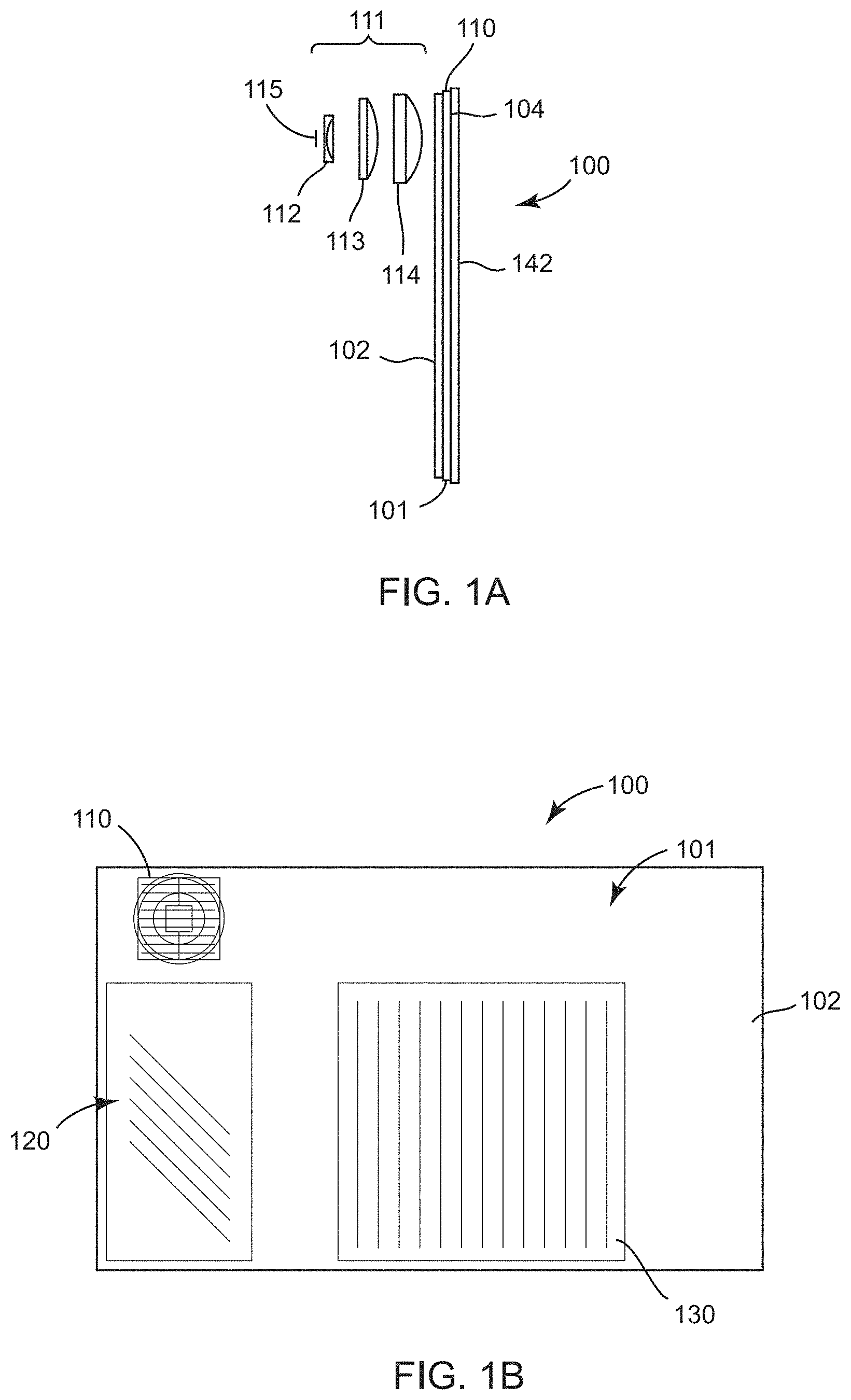
FIG. 1A is a planar side view schematic drawing of a dual axis expansion waveguide display system according to an exemplary embodiment;
FIG. 1B is a planar top view schematic drawing of the dual axis expansion waveguide display system illustrated in FIG. 1A according to an exemplary embodiment;
FIG. 2A is a planar top view schematic drawing of a dual axis expansion waveguide display system according to another exemplary embodiment;
FIG. 2B is a front view schematic illustration of the dual axis expansion waveguide display system illustrated in FIG. 2A according to another exemplary embodiment;
FIG. 2C is a top view schematic drawing of four output gratings forming a composite image by tiling four output images for the dual axis expansion waveguide display system illustrated in FIG. 2A according to another exemplary embodiment;
FIG. 2D is a side view schematic drawing of the dual axis expansion waveguide display system illustrated in FIG. 2A according to another exemplary embodiment;
FIG. 3A is a planar top view schematic drawing of a dual axis expansion waveguide display system according to another exemplary embodiment;
FIG. 3B is a front view schematic illustration of the dual axis expansion waveguide display system illustrated in FIG. 3A according to another exemplary embodiment; and
FIG. 3C is a top view schematic drawing of four output gratings forming a composite image by tiling four output images for the dual axis expansion waveguide display system illustrated in FIG. 3A according to another exemplary embodiment.
DETAILED DESCRIPTION
Following below are more detailed descriptions of various concepts related to, and embodiments of, an inventive optical display and methods for displaying information. It should be implemented in any of numerous ways, as the disclosed concepts are not limited to any particular manner of implementation. Examples of specific implementations and applications are provided primarily for illustrative purposes.
The invention will now be further described by way of example with reference to the accompanying drawings. It will be apparent to those skilled in the art that the present invention may be practiced with some or all of the present invention as disclosed in the following description. For the purposes of explaining the invention, well-known features of optical technology known to those skilled in the art of optical design and visual displays have been omitted or simplified in order not to obscure the basic principles of the invention. Unless otherwise stated, the term "on-axis" in relation to a ray or a beam direction refers to propagation parallel to an axis normal to the surfaces of the optical components described in relation to the invention. In the following description, the terms light, ray, beam and direction may be used interchangeably and in association with each other to indicate the direction of propagation of light energy along rectilinear trajectories. Parts of the following description will be presented using terminology commonly employed by those skilled in the art of optical design. It should also be noted that in the following description of the invention, repeated usage of the phrase "in one embodiment" does not necessarily refer to the same embodiment.
Referring generally to the Figures, systems and methods relating to near-eye display or head up display systems are shown according to various embodiments. Holographic waveguide technology can be advantageously utilized in waveguides for helmet mounted displays or head mounted displays (HMDs) and head up displays (HUDs) for many applications, including military applications and consumer applications (e.g., augmented reality glasses, etc.). Switchable Bragg gratings (SBGs), which are holograms recorded in holographic polymer dispersed liquid crystal, may be used in waveguides to create a larger field of view with increased resolution in current display systems, including HMDs, HUDs, and other near eye displays. SBGs may also be used to increase the field of view by tiling images presented sequentially on a micro display. A larger exit pupil may be created by using fold gratings in conjunction with conventional or other gratings to provide pupil expansion on a single waveguide in both the horizontal and vertical directions, thereby enabling the use of a very small lens system. Using the systems and methods disclosed herein, a single optical waveguide substrate may generate a wider field of view than found in current waveguide systems. Diffraction gratings may be used to split and diffract light rays into several beams that travel in different directions, thereby dispersing the light rays.
Referring to FIG. 1, an illustration of a dual axis (e.g., vertical and horizontal) beam expansion waveguide display system 100 is shown according to an exemplary embodiment. FIG. 1A is a planar side view schematic drawing of a dual axis expansion waveguide display system according to an exemplary embodiment. FIG. 1B is a planar top view schematic drawing of the dual axis expansion waveguide display system illustrated in FIG. 1A according to an exemplary embodiment. The waveguide display system 100 includes a substrate waveguide 101 and a light source 111. In some embodiments, the light from the light source 111 is polarized.
Substrate waveguide 101 includes a first surface 102, a second surface 104, an input coupler 110, a fold grating 120, and an output grating 130. The first and second surfaces 102 and 104 define the boundaries of the waveguide substrate 101 containing the fold grating 120 and the output grating 130 and are flat, planar surfaces in some embodiments. In some embodiments, waveguide substrate 101 can be a transmissive material, such as glass or plastic suitable for optical designs. The waveguide substrate 101 can be comprised of one or more layers and coatings.
Input coupler 110 can be a prism, mirror, reflective surface or grating for injecting light from the light source 111 into the waveguide substrate 101. In some embodiments, the input coupler 110 can be a holographic grating, such as a switchable or non-switchable SBG grating. Similarly, and in some embodiments, the fold grating 120 and the output grating 130 can be holographic gratings, such as switchable or non-switchable SBGs. As used herein, the term grating may encompass a grating comprised of a set of gratings in some embodiments.
The waveguide substrate 101 may include a number of layers. For example, in some embodiments, a first layer includes the fold grating 120 while a second layer includes the output grating 130. In some embodiments, a third layer can include input coupler 110. The number of layers may then be laminated together into a single waveguide substrate 101.
In some embodiments, the waveguide substrate 101 is comprised of a number of pieces including the input coupler 110, the fold grating 120 and the output grating 130 (or portions thereof) that are laminated together to form a single substrate waveguide. The pieces may be separated by optical glue or other transparent material of refractive index matching that of the pieces.
In another embodiment, the input coupler 110, the fold grating 120 and the output grating 130 can each be recorded into the same substrate to form the waveguide substrate 101. In another embodiment, the waveguide substrate 101 may be formed via a cell making process by creating cells of the desired grating thickness and vacuum filling each cell with SBG material for each of the input coupler 110, the fold grating 120 and the output grating 130. In one embodiment, the cell is formed by positioning multiple plates of glass with gaps between the plates of glass that define the desired grating thickness for the input coupler 110, the fold grating 120 and the output grating 130. In one embodiment, one cell may be made with multiple apertures such that the separate apertures are filled with different pockets of SBG material. Any intervening spaces may then be separated by a separating material (e.g., glue, oil, etc.) to define separate areas within a single substrate waveguide 101. In one embodiment, the SBG material may be spin-coated onto a substrate and then covered by a second substrate after curing of the material.
By using the fold grating 120, the waveguide display system 100 advantageously requires fewer layers than previous systems and methods of displaying information according to some embodiments. In addition, by using fold grating 120, light can travel by total internal refection within the substrate waveguide 101 in a single rectangular prism defined by surfaces 102 and 104 while achieving dual pupil expansion.
In another embodiment, the input coupler 110, the fold grating 120 and the output grating 130 can be created by interfering two waves of light at an angle within the substrate to create a holographic wave front, thereby creating light and dark fringes that are set in the waveguide substrate 101 at a desired angle. In one embodiment, the input coupler 110, the fold grating 120, and the output grating 130 embodied as holograms can be Bragg gratings recorded in a holographic polymer dispersed liquid crystal (HPDLC) (e.g., a matrix of liquid crystal droplets), although Bragg gratings may also be recorded in other materials. Bragg gratings recorded in HPDLC are known as SBGs. In one embodiment, SBGs are recorded in a special HPDLC material, such as POLICRYPS, resulting in a matrix of pure liquid crystal Bragg planes separated by solid polymer. SBGs may also be recorded in other materials, including POLIPHEM. Similar to POLICRYPS, POLIPHEM also provides a matrix of pure liquid crystal Bragg planes separated by solid polymer, however both substances are fabricated by different processes. The SBGs can be switching or non-switching in nature. In its non-switching form, an SBG has the advantage over conventional holographic photopolymer materials of being capable of providing high refractive index modulation due to its liquid crystal component.
The light source 111 can include a number of input objective lenses 112, 113, 114 and an image source 115 and can provide collimated light to the input coupler 110. The image source 115 can be a micro-display or laser based display. In one or more embodiments, the image source is a liquid crystal display (LCD) micro display or liquid crystal on silicon (LCOS) micro display.
In some embodiments, the input objective lenses 112, 113, 114 may be many different types of lenses, including, for example, projection lenses. In some embodiments, however, the light source 111 includes a single input objective lens (e.g., input objective lens 112). The input coupler 110 is configured to receive collimated light from a display source and to cause the light to travel within the substrate waveguide 101 via total internal reflection between the first surface 102 and the second surface 104 to the fold grating 120. The input objective lenses 112, 113, 114 collimate the display image on the image source 115 and each pixel on the image source 115 is converted into a unique angular direction within the substrate waveguide 101 according to some embodiments. The input coupler 110 may be orientated directly towards or at an angle relative to the fold grating 120. For example, in one embodiment, the input coupler 110 may be set at a slight incline in relation to the fold grating 120. One advantage of tilting the input coupler 110 is that the waveguide substrate 101 may also be tilted with respect to the viewer. For example, such tilting may allow the visor of FIG. 3B to provide a peripheral vision rather than a flat faceplate. Another benefit of using dual axis expansion in an optical waveguide is that smaller input objective lenses 112, 113, 114 may be used according to some embodiments. In some embodiments, at least one of the input objective lenses 112, 113, 114 may be a diffractive lens.
In some embodiments, the fold grating 120 may be oriented in a diagonal direction. The fold grating 120 is configured to provide pupil expansion in a first direction and to direct the light to the output grating 130 via total internal reflection between the first surface 102 and the second surface 104 of the substrate waveguide 101 in some embodiments. In one embodiment, a longitudinal edge of each fold grating 120 is oblique to the axis of alignment of the input coupler 110 such that each fold grating 120 is set on a diagonal with respect to the direction of propagation of the display light. The fold grating 120 is angled such that light from the input coupler 110 is redirected to the output grating 130. In one example, the fold grating 120 is set at a forty-five degree angle (e.g., 40-50 degrees) relative to the direction that the display image is released from the input coupler 110. This feature causes the display image propagating down the fold grating 120 to be turned into the output grating 130. For example, in one embodiment, the fold grating 120 causes the image to be turned 90 degrees into the output grating 130. In this manner, a single waveguide provides dual axis pupil expansion in both the horizontal and vertical directions. In one embodiment, each of the fold grating 120 may have a partially diffractive structure. In some embodiments, each of the fold grating 120 may have a fully diffractive structure. In some embodiments, different grating configurations and technologies may be incorporated in a single substrate waveguide 101.
The output grating 130 is configured to provide pupil expansion in a second direction different than the first direction and to cause the light to exit the waveguide 100 from the first surface or the second surface. The output grating 130 receives the display image from the fold grating 120 via total internal reflection and provides pupil expansion in a second direction. In some embodiments, the output grating 130 may consist of multiple layers of substrate, thereby comprising multiple layers of output gratings. Accordingly, there is no requirement for gratings to be in one plane within the substrate waveguide 101, and gratings may be stacked on top of each other (e.g., cells of gratings stacked on top of each other). The output grating 130 can be disposed approximately perpendicular to the gratings of the input couple 110 in some embodiments. In some embodiments, the output grating is disposed approximately 5-10 degrees (e.g., approximately 7.5 degrees) from the vertical axis.
In some embodiments, a quarter wave plate 142 on the substrate waveguide 101 rotates polarization of a light ray to maintain efficient coupling with the SBGs. The quarter wave plate 142 may be coupled to or adhered to the surface 102 of substrate waveguide 101. For example, in one embodiment, the quarter wave plate 142 is a coating that is applied to substrate waveguide 101. The quarter wave plate 142 provides light wave polarization management. Such polarization management may help light rays retain alignment with the intended viewing axis by compensating for skew waves in the substrate waveguide 101. In one embodiment, the output grating 130 may be contained by glass. The quarter wave plate 142 is optional and can increase the efficiency of the optical design in some embodiments. In some embodiments, the substrate waveguide 101 does not include the quarter wave plate 142. The quarter wave plate may be provided as a multi-layer coating.
Referring to FIGS. 2A-C, illustrations of a medium field of view head mounted display system 201 are shown according to an exemplary embodiment. FIG. 2A is a planar top view schematic drawing of one embodiment of a head mounted display system 201 including a dual axis (e.g., vertical and horizontal) beam expansion waveguide 200 and light sources 210 and 211. FIG. 2B is front view schematic illustration of an embodiment of the head mounted display system 201 being worn on a helmet, and FIG. 2C is a top view schematic drawing of four output gratings forming a composite image by tiling four output images for the head mounted display system 201 according to one embodiment. In one embodiment, the resolution of the composite image is formed by the tiling of four 800 by 600 images to create a composite 1600 by 1200 image in field of view space. The micro display input image may be updated synchronously with the switching of the SBGs. In some embodiments, the head mounted display system 201 provides a 30 degree by 40 degree field of view at the output grid 221 using multiplexing techniques such as those described in the applications incorporated herein by reference.
The light sources 210 and 211 may each include a number of input objective lenses 212 and image sources 215 that can provide collimated light. The image sources 215 can be micro displays or laser based displays, among other display types. In one or more embodiments, the image sources 215 are liquid crystal display (LCD) micro displays or liquid crystal on silicon (LCOS) micro displays. In one alternative embodiment, light sources 210 and 211 can be a single light source having two images for substrate waveguide 200.
In some embodiments, the input objective lenses 212 may be many different types of lenses, including, for example, projection lenses. In some embodiments, however, the light sources 210 and 211 include a single input objective lens. Pairs of input couplers on substrate waveguide 200, similar to input coupler 110, are each configured to receive collimated light from respective display sources 210 and 211 and to cause the light to travel within the substrate waveguide 200 via total internal reflection to respective fold gratings 254, 256, 258, and 260 similar to fold grating 120. The pairs of input couplers include a first pair of input couplers 214 and 216 associated with light source 210 (FIG. 2D). A second pair similar to the first pair is provided on substrate waveguide 201. The light from each respective fold grating 254, 256, 258, and 260 travels within the substrate waveguide 200 via total internal reflection to a respective output grating 224, 226, 228, and 230 similar to output grating 130 to form a respective image. FIG. 2A depicts output grating 224, 226, 228, and 230 as non-overlapping, however, it will be appreciated that the output gratings 224, 226, 228, and 230 overlap each other in some embodiments. FIG. 2A also depicts fold gratings 254, 258 as non-overlapping and fold gratings 256, 260 as non-overlapping, however, it will be appreciated that the fold gratings 254, 258, 256, and 260 may overlap in some embodiments. For example, in one embodiment, fold grating 254 and fold grating 258 overlap each other.
As shown in FIG. 2A, the substrate waveguide 200 may include the same or similar elements of the substrate waveguide 101 shown and described in relation to FIG. 1A, including fold gratings 254, 256, 258, and 260, and output gratings 224, 226, 228, and 230. In some embodiments, the head mounted display system 201 includes the light source 210 and the light source 211. Additional light sources can be utilized in some embodiments. As explained in further detail below, a light source 210 causes an image to travel from image source 215 to an input grating 214 or 216, which causes the image to travel within the substrate waveguide 200 via total internal reflection to one of fold gratings 254 or 258, which in turn causes the image to travel within the substrate waveguide 200 via total internal reflection to output grating 224 or 228, respectively. Multiplexing techniques are used such that an image is displayed by one output grating and then the other output grating to form half of a composite image. The multiplexing techniques can be used to turn gratings 214 and 216 on and off in a sequential fashion. Likewise, image source 211 causes an image to travel from image source 215 to a pair of input gratings similar to gratings 214 and 216, which then causes the image to travel within the substrate waveguide 200 via total internal reflection to one of fold gratings 256 or 260, which in turn causes the image to travel within the substrate waveguide 200 via total internal reflection to output grating 226 or 230, respectively. Multiplexing techniques are used such that an image is displayed by one output grating and then the other out grating to form half of a composite image. Together, the two half composite images form a full composite image. The gratings may be switchable and can be turned on and off, thereby deflecting light or not deflecting light, to effect multiplexing operations.
Referring to FIG. 2C, a top view schematic drawing of four output gratings forming a composite image by tiling four output images for the dual axis expansion waveguide display system illustrated in FIG. 2A is shown according to an exemplary embodiment. In some embodiments, output grid 221 includes four or more output gratings 224, 226, 228, and 230, each similar to output grating 130 and each corresponding to an output image that forms a composite image. In some embodiments, the output gratings 224, 226, 228, and 230 are switchable and can be turned on and off, thereby deflecting light or not deflecting light, to effect multiplexing operations. The output gratings 224, 226, 228, and 230 eject the light from the substrate waveguide 201 to the user. In some embodiments, the output grating 224 receives light from light source 210 via fold grating 254, output grating 228 receives light from light source 210 via fold grating 258, output grating 226 receives light from light source 211 via fold grating 256, and output grating 230 receives light from light source 211 via fold grating 260. In some embodiments, each output grating forms an image 20 by 15. Accordingly, each of light sources 210 and 211 forms an image 20 by 30. When the images formed by each light source are combined, a 40 by 30 composite image is formed. In the embodiment illustrated by FIG. 2C, each output grating 224, 226, 228, and 230 forms an image that is 800 pixels by 600 pixels, and when combined form a composite image that is 1600 pixels by 1200 pixels, however it will be appreciated that different configurations are possible. Although output grid 221 is shown as a 2 by 2 grid in a dual waveguide structure, other arrangements are possible. For example, a 3 by 2 grid can be provided on a waveguide structure including three layers or substrates. A 3 by 3 grid can be achieved using a waveguide structure including three layers or substrates and three fold gratings, three input gratings, and three output gratings per layer or substrate and three light sources, and so on. By including the light source 210 and the light source 211, the substrate waveguide 200 may create a full field of view or larger field of view. The composite image may also include an origin 238 positioned in front of a pupil of an eye of a user.
Referring to FIG. 2D, a side view schematic drawing of the dual axis expansion waveguide display system 201 illustrated in FIG. 2A is shown according to another exemplary embodiment. As shown in FIG. 2D, only half the dual axis expansion waveguide display system 201 illustrated in FIG. 2A is shown. In one embodiment, the substrate waveguide 200 may include multiple layers, such as first layer 207 and second layer 209, however it will be appreciated that additional layers, or even a single layer, may be used. In one embodiment, fold grating 228 and output grating 258 are located in the same plane within first layer 207, and therefore overlap in FIG. 2D. Similarly, fold grating 254 and output grating 224 are located in the same plane within second layer 209 and therefore overlap in FIG. 2D. The light source 210 causes an image to travel from the image source 215 to input grating 214, which causes the image to travel within the substrate waveguide 200 via total internal reflection to fold grating 254 (FIG. 2A), which in turn cause the image to travel within the substrate waveguide 200 within first layer 207 via total internal reflection to output grating 228. Likewise, the light source 210 causes an image to travel from the image source 215 to input grating 216, which causes the image to travel within the substrate waveguide 200 within second layer 209 via total internal reflection to fold gratings 224 (FIG. 2A), which in turn cause the image to travel within the substrate waveguide 200 within second layer 209 via total internal reflection to output grating 224. The images from light source 211 are provided to fold gratings 256 and 260 and output gratings 226 and 230 in a similar fashion as described above with respect to light source 210. Multiplexing techniques are used such that an image is displayed by one output grating and then the other output grating to form half of a composite image. Together, the two half composite images form a full composite image. The gratings may be switchable and can be turned on and off, thereby deflecting light or not deflecting light, to effect multiplexing operations.
Referring to FIGS. 3A-C, illustrations of a medium field of view goggle display system 301 is shown according to an exemplary embodiment. FIG. 3A is a planar top view schematic drawing of one embodiment of the goggle display system 301 including a dual axis (e.g., vertical and horizontal) beam expansion waveguide 300 and light sources 310 and 311. FIG. 3B is a front view schematic illustration of an embodiment of the goggle display system 301 being worn on a helmet, and FIG. 3C is a planar top view schematic drawing of an output grid 321 for the goggle display system 301, according to one embodiment. In some embodiments, the goggle display system 301 provides a 40 degree by 30 degree field of view at the output grid 321 using multiplexing techniques such as those described in the applications incorporated herein by reference.
As shown in FIG. 3A, the substrate waveguide 300 may include the same or similar elements of the substrate waveguide 200 shown and described in relation to FIGS. 2A-C. In some embodiments, the goggle display system 301 includes the light source 310 and the light source 311. Additional light sources can be utilized in some embodiments.
The light sources 310 and 311 may each include a number of input objective lenses 312 and image sources 315 that can provide collimated light. The image sources 315 can be micro displays or laser based displays, among other display types. In one or more embodiments, the image sources 315 are liquid crystal display (LCD) micro displays or liquid crystal on silicon (LCOS) micro displays. In one alternative embodiment, light sources 310 and 311 can be a single light source having two images for substrate waveguide 300.
In some embodiments, the input objective lenses 312 may be many different types of lenses, including, for example, projection lenses. In some embodiments, however, the light sources 310 and 311 include a single input objective lens. A pair of input couplers on substrate waveguide 300, similar to input coupler 110, are each configured to receive collimated light from respective display sources 310 and 311 and to cause the light to travel within the substrate waveguide 300 via total internal reflection to a respective fold grating similar to fold grating 120. The light from each respective fold grating travels within the substrate waveguide 300 via total internal reflection to output grid 321.
In some embodiments, output grid 321 includes four or more output gratings 324, 326, 328, and 330, each similar to output grating 130. In some embodiments, the output gratings 324, 326, 328, and 330 are switchable and can be turned on and off to effect multiplexing operations. The output gratings 324, 326, 328, and 330 eject the light from the substrate waveguide 300 to the user. In some embodiments, the output gratings 324 and 326 receive light from the first fold grating in substrate waveguide 300 and light source 310, and the output gratings 328 and 330 receive light from the second fold grating in substrate waveguide 300 and light source 311.
By including the light source 310 and the light source 311, the substrate waveguide 300 may create a full field of view or larger field of view. In some embodiments, the substrate waveguide 300 creates a full field of view or larger field of view using multiplexing techniques. For example, FIG. 3C illustrates an embodiment similar to that of FIG. 2C, except that the composite images are displayed in a horizontal orientation. In some embodiments, each output grating forms an image 15 by 20. Accordingly, each of light sources 310 and 311 forms an image 30 by 20. When the images formed by each light source are combined, a 30 by 40 composite image is formed. In the embodiment illustrated by FIG. 3C, each output grating 324, 326, 328, and 330 forms an image that is 600 pixels by 800 pixels, and when combined form a composite image that is 1200 pixels by 1600 pixels, however it will be appreciated that different configurations are possible. Although output grid 321 is shown as a 2 by 2 grid in a dual waveguide structure, other arrangements are possible. For example, a 3 by 2 grid can be provided on a waveguide structure including three layers or substrates. A 3 by 3 grid can be achieved using a waveguide structure including three layers or substrates and three fold gratings, three input gratings, and three output gratings per layer or substrate and three light sources, and so on. By including the light source 310 and the light source 311, the substrate waveguide 300 may create a full field of view or larger field of view. The composite image may also include an origin positioned in front of a pupil of an eye of a user.
In some embodiments, this configuration is utilized in a head mounted display goggle as shown in FIG. 3B, for example, a sand wind and dust goggle. In some embodiments, the output waveguide SBGs are displaced so that they line up with the eye location in the goggle. In some embodiments, an origin of grid 321 is positioned in front of a pupil of the eye of the user.
The construction and arrangement of the systems and methods as shown in the various exemplary embodiments are illustrative only. Although only a few embodiments have been described in detail in this disclosure, many modifications are possible (e.g., variations in sizes, dimensions, structures, shapes and proportions of the various elements, values of parameters, mounting arrangements, use of materials, colors, orientations, etc.). For example, the position of elements may be reversed or otherwise varied and the nature or number of discrete elements or positions may be altered or varied. Accordingly, all such modifications are intended to be included within the scope of the present disclosure. The order or sequence of any process or method steps may be varied or re-sequenced according to alternative embodiments. Other substitutions, modifications, changes, and omissions may be made in the design, operating conditions and arrangement of the exemplary embodiments without departing from the scope of the present disclosure.
Although the figures may show a specific order of method steps, the order of the steps may differ from what is depicted. Also two or more steps may be performed concurrently or with partial concurrence. Such variation will depend on the software and hardware systems chosen and on designer choice. All such variations are within the scope of the disclosure.
* * * * *
References
D00000
D00001
D00002
D00003
XML
uspto.report is an independent third-party trademark research tool that is not affiliated, endorsed, or sponsored by the United States Patent and Trademark Office (USPTO) or any other governmental organization. The information provided by uspto.report is based on publicly available data at the time of writing and is intended for informational purposes only.
While we strive to provide accurate and up-to-date information, we do not guarantee the accuracy, completeness, reliability, or suitability of the information displayed on this site. The use of this site is at your own risk. Any reliance you place on such information is therefore strictly at your own risk.
All official trademark data, including owner information, should be verified by visiting the official USPTO website at www.uspto.gov. This site is not intended to replace professional legal advice and should not be used as a substitute for consulting with a legal professional who is knowledgeable about trademark law.