Holographic Waveguides Incorporating Birefringence Control and Methods for Their Fabrication
Waldern; Jonathan David ; et al.
U.S. patent application number 16/906872 was filed with the patent office on 2020-10-08 for holographic waveguides incorporating birefringence control and methods for their fabrication. This patent application is currently assigned to DigiLens Inc.. The applicant listed for this patent is DigiLens Inc.. Invention is credited to Alastair John Grant, Milan Momcilo Popovich, Jonathan David Waldern.
| Application Number | 20200319404 16/906872 |
| Document ID | / |
| Family ID | 1000004906019 |
| Filed Date | 2020-10-08 |


View All Diagrams
| United States Patent Application | 20200319404 |
| Kind Code | A1 |
| Waldern; Jonathan David ; et al. | October 8, 2020 |
Holographic Waveguides Incorporating Birefringence Control and Methods for Their Fabrication
Abstract
Many embodiments in accordance with the invention are directed towards waveguides implementing birefringence control. In some embodiments, the waveguide includes a birefringent grating layer and a birefringence control layer. In further embodiments, the birefringence control layer is compact and efficient. Such structures can be utilized for various applications, including but not limited to: compensating for polarization related losses in holographic waveguides; providing three-dimensional LC director alignment in waveguides based on Bragg gratings; and spatially varying angular/spectral bandwidth for homogenizing the output from a waveguide. In some embodiments, a polarization-maintaining, wide-angle, and high-reflection waveguide cladding with polarization compensation is implemented for grating birefringence. In several embodiments, a thin polarization control layer is implemented for providing either quarter wave or half wave retardation.
| Inventors: | Waldern; Jonathan David; (Los Altos Hills, CA) ; Popovich; Milan Momcilo; (Leicester, GB) ; Grant; Alastair John; (San Jose, CA) | ||||||||||
| Applicant: |
|
||||||||||
|---|---|---|---|---|---|---|---|---|---|---|---|
| Assignee: | DigiLens Inc. Sunnyvale CA |
||||||||||
| Family ID: | 1000004906019 | ||||||||||
| Appl. No.: | 16/906872 | ||||||||||
| Filed: | June 19, 2020 |
Related U.S. Patent Documents
| Application Number | Filing Date | Patent Number | ||
|---|---|---|---|---|
| 16357233 | Mar 18, 2019 | 10690851 | ||
| 16906872 | ||||
| 62643977 | Mar 16, 2018 | |||
| Current U.S. Class: | 1/1 |
| Current CPC Class: | G02B 6/34 20130101; G02B 2006/12116 20130101; G02B 6/126 20130101; G02B 6/13 20130101; G02B 6/274 20130101; G02B 6/1221 20130101 |
| International Class: | G02B 6/126 20060101 G02B006/126; G02B 6/13 20060101 G02B006/13; G02B 6/34 20060101 G02B006/34; G02B 6/27 20060101 G02B006/27 |
Claims
1. A waveguide comprising: at least one waveguide substrate; at least one birefringent grating; at least one birefringence control layer; a light source for outputting light; an input coupler for directing the light into total internal reflection paths within the waveguide; and an output coupler for extracting light from the waveguide, wherein the interaction of the light with the birefringence control layer and the birefringent grating provides a predefined characteristic of light extracted from the waveguide.
2. The waveguide of claim 1, wherein the interaction of light with the birefringence control layer provides at least one of: an angular or spectral bandwidth variation; a polarization rotation; a birefringence variation; an angular or spectral dependence of at least one of beam transmission or polarization rotation; and a light transmission variation in at least one direction in the plane of the waveguide substrate.
3. The waveguide of claim 1, wherein the predefined characteristic varies across the waveguide.
4. The waveguide of claim 1, wherein the predefined characteristic results from the cumulative effect of the interaction of the light with the birefringence control layer and the birefringent grating along at least one direction of light propagation within the waveguide.
5. The waveguide of claim 1, wherein the predefined characteristic comprises at least one of: uniform illumination and uniform polarization over the angular range of the light.
6. The waveguide of claim 1, wherein the birefringence control layer provides compensation for polarization rotation introduced by the birefringent grating along at least one direction of light propagation within the waveguide.
7. The waveguide of claim 1, wherein the birefringence control layer is a liquid crystal and polymer material system.
8. The waveguide of claim 1, wherein the birefringence control layer is a liquid crystal and polymer system aligned using directional ultraviolet radiation.
9. The waveguide of claim 1, wherein the birefringence control layer is aligned by at least one of: electromagnetic radiation; electrical or magnetic fields; mechanical forces; chemical reaction; and thermal exposure.
10. The waveguide of claim 1, wherein the birefringence control layer influences the alignment of LC directors in a birefringent grating formed in a liquid crystal and polymer system.
11. The waveguide of claim 1, wherein the birefringence control layer has an anisotropic refractive index.
12. The waveguide of claim 1, wherein the birefringence control layer is formed on at least one internal or external optical surface of the waveguide.
13. The waveguide of claim 1, wherein the birefringence control layer comprises at least one stack of refractive index layers disposed on at least one optical surface of the waveguide, wherein at least one layer in the stack of refractive index layers has an isotropic refractive index and at least one layer in the stack of refractive index layers has an anisotropic refractive index.
14. The waveguide of claim 1, wherein the birefringence control layer provides a high reflection layer.
15. The waveguide of claim 1, wherein the birefringence control layer provides optical power.
16. The waveguide of claim 1, wherein the birefringence control layer provides an environmental isolation layer for the waveguide.
17. The waveguide of claim 1, wherein the birefringence control layer has a gradient index structure.
18. The waveguide of claim 1, wherein the birefringence control layer is formed by stretching a layer of an optical material to spatially vary its refractive index in the plane of the waveguide substrate.
19. The waveguide of claim 1, wherein the light source provides collimated light in angular space.
20. The waveguide of claim 1, wherein at least one of the input coupler and output coupler comprises a birefringent grating.
Description
CROSS-REFERENCE TO RELATED APPLICATIONS
[0001] The current application is a continuation of U.S. patent application Ser. No. 16/357,233 entitled "Holographic Waveguides Incorporating Birefringence Control and Methods for Their Fabrication," filed Mar. 18, 2019, which claims the benefit of and priority under 35 U.S.C. .sctn. 119(e) to U.S. Provisional Patent Application No. 62/643,977 entitled "Holographic Waveguides Incorporating Birefringence Control and Methods for Their Fabrication," filed Mar. 16, 2018. The disclosure of U.S. Provisional Patent Application No. 62/643,977 is hereby incorporated by reference in its entirety for all purposes.
FIELD OF THE INVENTION
[0002] The present disclosure relates to optical waveguides and more particularly to waveguide displays using birefringent gratings.
BACKGROUND OF THE INVENTION
[0003] Waveguides can be referred to as structures with the capability of confining and guiding waves (i.e., restricting the spatial region in which waves can propagate). One subclass includes optical waveguides, which are structures that can guide electromagnetic waves, typically those in the visible spectrum. Waveguide structures can be designed to control the propagation path of waves using a number of different mechanisms. For example, planar waveguides can be designed to utilize diffraction gratings to diffract and couple incident light into the waveguide structure such that the in-coupled light can proceed to travel within the planar structure via total internal reflection ("TIR").
[0004] Fabrication of waveguides can include the use of material systems that allow for the recording of holographic optical elements within the waveguides. One class of such material includes polymer dispersed liquid crystal ("PDLC") mixtures, which are mixtures containing photopolymerizable monomers and liquid crystals. A further subclass of such mixtures includes holographic polymer dispersed liquid crystal ("HPDLC") mixtures. Holographic optical elements, such as volume phase gratings, can be recorded in such a liquid mixture by illuminating the material with two mutually coherent laser beams. During the recording process, the monomers polymerize and the mixture undergoes a photopolymerization-induced phase separation, creating regions densely populated by liquid crystal micro-droplets, interspersed with regions of clear polymer. The alternating liquid crystal-rich and liquid crystal-depleted regions form the fringe planes of the grating.
[0005] Waveguide optics, such as those described above, can be considered for a range of display and sensor applications. In many applications, waveguides containing one or more grating layers encoding multiple optical functions can be realized using various waveguide architectures and material systems, enabling new innovations in near-eye displays for augmented reality ("AR") and virtual reality ("VR"), compact heads-up displays ("HUDs") for aviation and road transport, and sensors for biometric and laser radar ("LIDAR") applications.
SUMMARY OF THE INVENTION
[0006] Following below are more detailed descriptions of various concepts related to, and embodiments of, an inventive optical display and methods for displaying information. It should be appreciated that various concepts introduced above and discussed in greater detail below may be implemented in any of numerous ways, as the disclosed concepts are not limited to any particular manner of implementation. Examples of specific implementations and applications are provided primarily for illustrative purposes. A more complete understanding of the invention can be obtained by considering the following detailed description in conjunction with the accompanying drawings, wherein like index numerals indicate like parts. For purposes of clarity, details relating to technical material that is known in the technical fields related to the invention have not been described in detail.
[0007] One embodiment includes a waveguide including at least one waveguide substrate, at least one birefringent grating; at least one birefringence control layer, a light source for outputting light, an input coupler for directing the light into total internal reflection paths within the waveguide, and an output coupler for extracting light from the waveguide, wherein the interaction of the light with the birefringence control layer and the birefringent grating provides a predefined characteristic of light extracted from the waveguide.
[0008] In another embodiment, the interaction of light with the birefringence control layer provides at least one of: an angular or spectral bandwidth variation, a polarization rotation, a birefringence variation, an angular or spectral dependence of at least one of beam transmission or polarization rotation, and a light transmission variation in at least one direction in the plane of the waveguide substrate.
[0009] In a further embodiment, the predefined characteristic varies across the waveguide.
[0010] In still another embodiment, the predefined characteristic results from the cumulative effect of the interaction of the light with the birefringence control layer and the birefringent grating along at least one direction of light propagation within the waveguide.
[0011] In a still further embodiment, the predefined characteristic includes at least one of: uniform illumination and uniform polarization over the angular range of the light.
[0012] In yet another embodiment, the birefringence control layer provides compensation for polarization rotation introduced by the birefringent grating along at least one direction of light propagation within the waveguide.
[0013] In a yet further embodiment, the birefringence control layer is a liquid crystal and polymer material system.
[0014] In another additional embodiment, the birefringence control layer is a liquid crystal and polymer system aligned using directional ultraviolet radiation.
[0015] In a further additional embodiment, the birefringence control layer is aligned by at least one of: electromagnetic radiation, electrical or magnetic fields, mechanical forces, chemical reaction, and thermal exposure.
[0016] In another embodiment again, the birefringence control layer influences the alignment of LC directors in a birefringent grating formed in a liquid crystal and polymer system.
[0017] In a further embodiment again, the birefringence control layer has an anisotropic refractive index.
[0018] In still yet another embodiment, the birefringence control layer is formed on at least one internal or external optical surface of the waveguide.
[0019] In a still yet further embodiment, the birefringence control layer includes at least one stack of refractive index layers disposed on at least one optical surface of the waveguide, wherein at least one layer in the stack of refractive index layers has an isotropic refractive index and at least one layer in the stack of refractive index layers has an anisotropic refractive index.
[0020] In still another additional embodiment, the birefringence control layer provides a high reflection layer.
[0021] In a still further additional embodiment, the birefringence control layer provides optical power.
[0022] In still another embodiment again, the birefringence control layer provides an environmental isolation layer for the waveguide.
[0023] In a still further embodiment again, the birefringence control layer has a gradient index structure.
[0024] In yet another additional embodiment, the birefringence control layer is formed by stretching a layer of an optical material to spatially vary its refractive index in the plane of the waveguide substrate.
[0025] In a yet further additional embodiment, the light source provides collimated light in angular space.
[0026] In yet another embodiment again, at least one of the input coupler and output coupler includes a birefringent grating.
[0027] In a yet further embodiment again, the birefringent grating is recorded in a material system including at least one polymer and at least one liquid crystal.
[0028] In another additional embodiment again, the at least one birefringent grating includes at least one birefringent grating for providing at least one of the functions of: beam expansion in a first direction, beam expansion in a second direction and light extraction from the waveguide, and coupling light from the source into a total internal reflection path in the waveguide.
[0029] In a further additional embodiment again, the light source includes a laser, and the alignment of LC directors in the birefringent grating spatially vary to compensate for illumination banding.
[0030] A still yet another additional embodiment includes a method of fabricating a waveguide, the method including providing a first transparent substrate, depositing a layer of grating recording material, exposing the layer of grating recording material to form a grating layer, forming a birefringence control layer, and applying a second transparent substrate.
[0031] In a still yet further additional embodiment, the layer of grating recording material is deposited onto the substrate, the birefringence control layer is formed on the grating layer, and the second transparent substrate is applied over the birefringence control layer.
[0032] In yet another additional embodiment again, the layer of grating recording material is deposited onto the substrate, the second transparent substrate is applied over the grating layer, and the birefringence control layer is formed on second transparent substrate.
[0033] In a yet further additional embodiment again, the birefringence control layer is formed on the first transparent substrate, the layer of grating recording material is deposited onto the birefringence control layer, and the second transparent substrate is applied over the grating layer.
[0034] In still yet another embodiment again, the method further includes depositing a layer of liquid crystal polymer material and aligning the liquid crystal polymer material using directional UV light, wherein the layer of grating recording material is deposited onto the substrate and the second transparent substrate is applied over the aligned liquid crystal polymer layer.
[0035] In a still yet further embodiment again, the layer of liquid crystal polymer material is deposited onto one of either the grating layer or the second transparent substrate.
[0036] In still yet another additional embodiment again, the layer of liquid crystal polymer material is deposited onto the first transparent substrate, the layer of grating recording material is deposited onto the aligned liquid crystal polymer material, and the second transparent substrate is applied over the grating layer.
[0037] Additional embodiments and features are set forth in part in the description that follows, and in part will become apparent to those skilled in the art upon examination of the specification or may be learned by the practice of the invention. A further understanding of the nature and advantages of the present invention may be realized by reference to the remaining portions of the specification and the drawings, which forms a part of this disclosure.
BRIEF DESCRIPTION OF THE DRAWINGS
[0038] These and other features and advantages of the present invention will be better understood by reference to the following detailed description when considered in conjunction with the accompanying data and figures, wherein:
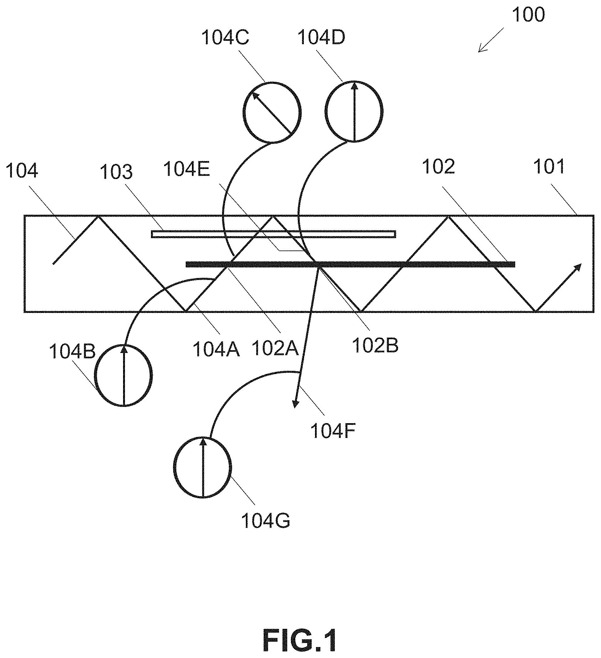
[0039] FIG. 1 conceptually illustrates a schematic cross section view of a waveguide incorporating a birefringent grating and birefringence control layer in accordance with an embodiment of the invention.
[0040] FIG. 2 conceptually illustrates a schematic cross section view of a waveguide incorporating a birefringent grating and birefringence control layer for compensating grating birefringence in accordance with some embodiments of the invention.
[0041] FIG. 3 conceptually illustrates a schematic cross section view of a waveguide incorporating a birefringent grating and birefringence control layer for providing uniform output illumination from the waveguide in accordance with an embodiment of the invention.
[0042] FIG. 4 conceptually illustrates a schematic cross section view of a birefringence control layer formed by a multilayer structure combining isotropic and anisotropic index layers in accordance with an embodiment of the invention.
[0043] FIG. 5 conceptually illustrates a schematic cross section view of a birefringence control layer formed by a multilayer structure combining isotropic and anisotropic index layers integrated with a birefringent grating layer in accordance with an embodiment of the invention.
[0044] FIG. 6 conceptually illustrates a plan view of a dual expansion waveguide with birefringent control layers in accordance with an embodiment of the invention.
[0045] FIG. 7 conceptually illustrates a schematic cross section view of a waveguide incorporating a birefringent grating and birefringence control layer for correcting birefringence introduced by an optical element in the output light path from the waveguide in accordance with an embodiment of the invention.
[0046] FIG. 8 conceptually illustrates a schematic plan view of an apparatus for aligning a birefringence control layer by applying forces to the edges of the layer in accordance with an embodiment of the invention.
[0047] FIGS. 9A-9F conceptually illustrate the process steps and apparatus for fabricating a waveguide containing a birefringent grating and a birefringence control layer in accordance with various embodiments of the invention.
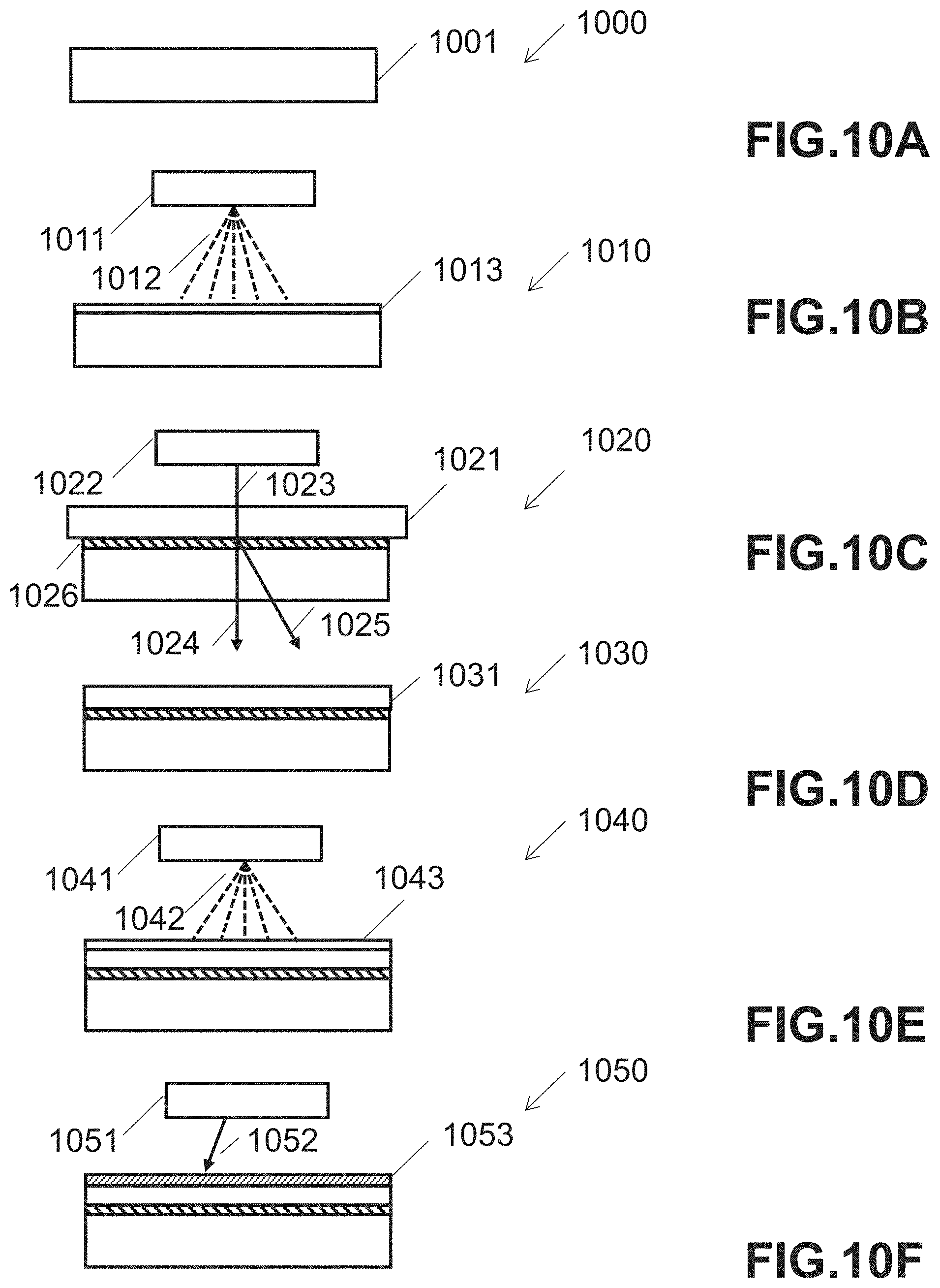
[0048] FIGS. 10A-10F conceptually illustrate the process steps and apparatus for fabricating a waveguide containing a birefringent grating with a birefringence control layer applied to an outer surface of the waveguide in accordance with various embodiments of the invention.
[0049] FIGS. 11A-11F conceptually illustrate the process steps and apparatus for fabricating a waveguide containing a birefringent grating and a birefringence control layer in accordance with various embodiments of the invention.
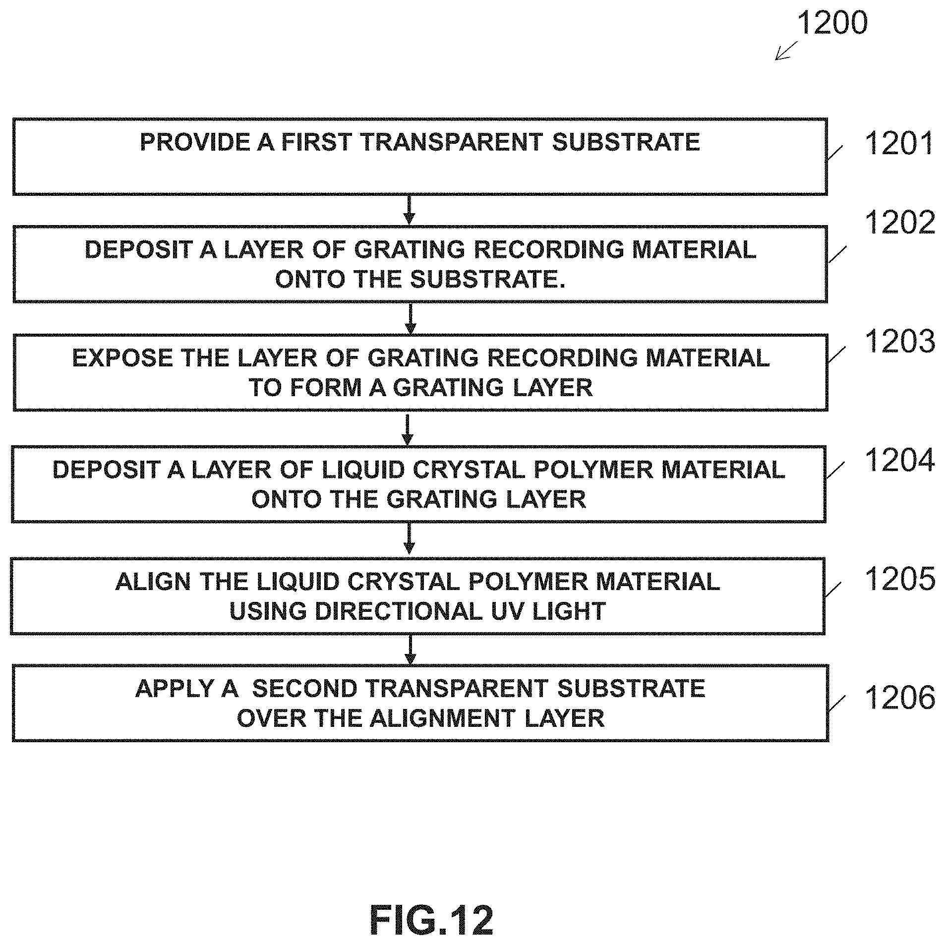
[0050] FIG. 12 conceptually illustrates a flow chart showing a method of fabricating a waveguide containing a birefringent grating and a birefringence control layer in accordance with an embodiment of the invention.
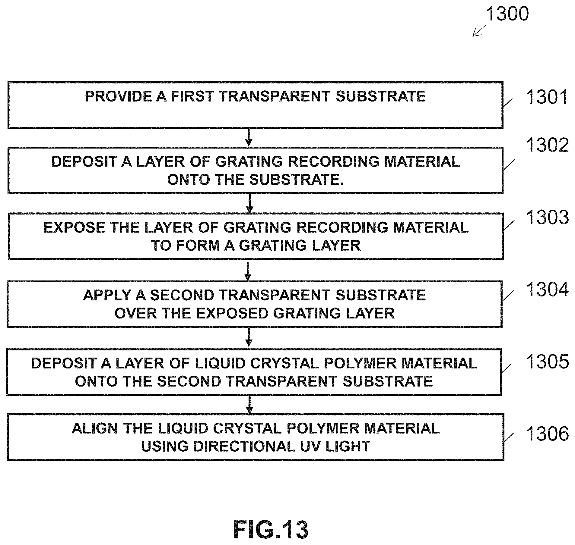
[0051] FIG. 13 conceptually illustrates a flow chart showing a method of fabricating a waveguide containing a birefringent grating and a birefringence control layer applied to an outer surface of the waveguide in accordance with an embodiment of the invention.
[0052] FIG. 14 conceptually illustrates a flow chart showing a method of fabricating a waveguide containing a birefringent grating and a birefringence control layer where forming the birefringence control layer is carried out before the recording of the grating layer in accordance with an embodiment of the invention.
[0053] FIG. 15 conceptually illustrates a schematic side view of a waveguide with a birefringence control layer applied at the waveguide to air interface in accordance with an embodiment of the invention.
[0054] FIG. 16 conceptually illustrates a schematic side view of a waveguide with a birefringence control layer that isolates the waveguide from its environment applied to the waveguide to air interface in accordance with an embodiment of the invention.
[0055] FIG. 17 conceptually illustrates a schematic side view of an apparatus for fabricating a structure containing a birefringent grating layer overlaying a birefringence control layer where the grating recording beams propagate through the birefringence control layer in accordance with an embodiment of the invention.
[0056] FIG. 18 conceptually illustrates a schematic side view of an apparatus for fabricating a structure containing a birefringence control layer overlaying a birefringent grating layer where the birefringence control layer is aligned by UV radiation propagating through the grating in accordance with an embodiment of the invention.
[0057] FIG. 19 conceptually illustrates a cross section of waveguide containing substrates sandwiching a grating layer.
[0058] FIG. 20 conceptually illustrates a waveguide with a quarter wave polarization layer inserted in accordance with an embodiment of the invention.
[0059] FIG. 21 conceptually illustrates a schematic cross section view showing a portion of a waveguide illustrating the use of a quarter wave polarization layer with a RKV grating in accordance with an embodiment of the invention.
[0060] FIG. 22 conceptually illustrates a polarization layer architecture containing an LCP quarter wave cell and a reactive monomer liquid crystal mixture (RMLCM) cell separated by index matching oil layer in accordance with an embodiment of the invention.
[0061] FIG. 23 conceptually illustrates an example of a polarization architecture based on a grating cell with the RMLCM grating material layer in direct contact with a bare LCP film in accordance with an embodiment of the invention.
[0062] FIG. 24 conceptually illustrates a cross section view schematically showing an example of polarization layer architecture in which a bare LCP layer is bonded to a bare RMLCM layer in accordance with an embodiment of the invention.
[0063] FIG. 25 conceptually illustrates a cross section view schematically showing an example of a polarization layer architecture using a RMLCM layer as a polarization layer in accordance with an embodiment of the invention.
[0064] FIG. 26 conceptually illustrates an example of a polarization layer architecture that includes a feature for compensating for polarization rotation introduced by birefringent gratings in accordance with an embodiment of the invention.
[0065] FIG. 27 conceptually illustrates a plan view schematically showing a waveguide display incorporating the features of the embodiment of FIG. 26 in accordance with an embodiment of the invention.
[0066] FIGS. 28 and 29 conceptually illustrate cross section views schematically showing examples of polarization layer architectures containing an upper substrate, an LCP layer with hard encapsulation layer, a RMLCM layer, and a lower substrate in accordance with various embodiments of the invention.
[0067] FIG. 30 conceptually illustrates a plan view schematically showing a first example of a two-region polymer film in accordance with an embodiment of the invention.
[0068] FIG. 31 conceptually illustrates a plan view schematically showing a second example of a two-region polymer film in accordance with an embodiment of the invention.
[0069] FIG. 32 conceptually illustrates a plan view schematically showing a third example of a two-region polymer film in accordance with an embodiment of the invention.
[0070] FIG. 33 conceptually illustrates a drawing showing a clear aperture layout in accordance with an embodiment of the invention.
[0071] FIG. 34 conceptually illustrates a plan view schematically showing a waveguide containing input, fold, and output gratings including the K-vectors and alignment layer fast axis directions for each grating in accordance with an embodiment of the invention.
DETAILED DESCRIPTION OF THE INVENTION
[0072] For the purposes of describing embodiments, some well-known features of optical technology known to those skilled in the art of optical design and visual displays have been omitted or simplified in order to not obscure the basic principles of the invention. Unless otherwise stated, the term "on-axis" in relation to a ray or a beam direction refers to propagation parallel to an axis normal to the surfaces of the optical components described in relation to the invention. In the following description the terms light, ray, beam, and direction may be used interchangeably and in association with each other to indicate the direction of propagation of electromagnetic radiation along rectilinear trajectories. The term light and illumination may be used in relation to the visible and infrared bands of the electromagnetic spectrum. Parts of the following description will be presented using terminology commonly employed by those skilled in the art of optical design. In the following description, the term grating may be used to refer to any kind of diffractive structure used in a waveguide, including holograms and Bragg or volume holograms. The term grating may also encompass a grating that includes of a set of gratings. For example, in some embodiments the input grating and output grating each include two or more gratings multiplexed into a single layer. For illustrative purposes, it is to be understood that the drawings are not drawn to scale unless stated otherwise.
[0073] Referring generally to the drawings, systems and methods relating to waveguide applications incorporating birefringence control in accordance with various embodiments of the invention are illustrated. Birefringence is the optical property of a material having a refractive index that depends on the polarization and propagation direction of light. A birefringent grating can be referred to as a grating having such properties. In many cases, the birefringent grating is formed in a liquid crystal polymer material system such as but not limited to HPDLC mixtures. The polarization properties of such a grating can depend on average relative permittivity and relative permittivity modulation tensors.
[0074] Many embodiments in accordance with the invention are directed towards waveguides implementing birefringence control. In some embodiments, the waveguide includes a birefringent grating layer and a birefringence control layer. In further embodiments, the birefringence control layer is compact and efficient. Such structures can be utilized for various applications, including but not limited to: compensating for polarization related losses in holographic waveguides; providing three-dimensional LC director alignment in waveguides based on Bragg gratings; and spatially varying angular/spectral bandwidth for homogenizing the output from a waveguide. In some embodiments, a polarization-maintaining, wide-angle, and high-reflection waveguide cladding with polarization compensation is implemented for grating birefringence. In several embodiments, a thin polarization control layer is implemented for providing either quarter wave or half wave retardation. In a number of embodiments, a polarization-maintaining, wide-angle birefringence control layer is implemented for modifying the polarization output of a waveguide to balance the birefringence of an external optical element used with the waveguide.
[0075] In many embodiments, the waveguide includes at least one input grating and at least one output grating. In further embodiments, the waveguide can include additional gratings for various purposes, such as but not limited to fold gratings for beam expansion. The input grating and output grating may each include multiplexed gratings. In some embodiments, the input grating and output grating may each include two overlapping gratings layers that are in contact or vertically separated by one or more thin optical substrate. In some embodiments, the grating layers are sandwiched between glass or plastic substrates. In some embodiments two or more such gratings layers may form a stack within which total internal reflection occurs at the outer substrate and air interfaces. In some embodiments, the waveguide may include just one grating layer. In some embodiments, electrodes may be applied to faces of the substrates to switch gratings between diffracting and clear states. The stack may further include additional layers such as beam splitting coatings and environmental protection layers. The input and output gratings shown in the drawings may be provided by any of the above described grating configurations. Advantageously, the input and output gratings can be designed to have common surface grating pitch. In cases where the waveguide contains grating(s) in addition to the input and output gratings, the gratings can be designed to have grating pitches such that the vector sum of the grating vectors is substantially zero. The input grating can combine gratings orientated such that each grating diffracts a polarization of the incident unpolarized light into a waveguide path. The output gratings can be configured in a similar fashion such that the light from the waveguide paths is combined and coupled out of the waveguide as unpolarized light. Each grating is characterized by at least one grating vector (or K-vector) in 3D space, which in the case of a Bragg grating is defined as the vector normal to the Bragg fringes. The grating vector can determine the optical efficiency for a given range of input and diffracted angles. In some embodiments, the waveguide includes at least one surface relief grating. Waveguide gratings structures, materials systems, and birefringence control are discussed below in further detail.
[0076] Switchable Bragg Gratings
[0077] Optical structures recorded in waveguides can include many different types of optical elements, such as but not limited to diffraction gratings. In many embodiments, the grating implemented is a Bragg grating (also referred to as a volume grating). Bragg gratings can have high efficiency with little light being diffracted into higher orders. The relative amount of light in the diffracted and zero order can be varied by controlling the refractive index modulation of the grating, a property that is can be used to make lossy waveguide gratings for extracting light over a large pupil. One class of gratings used in holographic waveguide devices is the Switchable Bragg Grating ("SBG"). SBGs can be fabricated by first placing a thin film of a mixture of photopolymerizable monomers and liquid crystal material between glass plates or substrates. In many cases, the glass plates are in a parallel configuration. One or both glass plates can support electrodes, typically transparent tin oxide films, for applying an electric field across the film. The grating structure in an SBG can be recorded in the liquid material (often referred to as the syrup) through photopolymerization-induced phase separation using interferential exposure with a spatially periodic intensity modulation. Factors such as but not limited to control of the irradiation intensity, component volume fractions of the materials in the mixture, and exposure temperature can determine the resulting grating morphology and performance. As can readily be appreciated, a wide variety of materials and mixtures can be used depending on the specific requirements of a given application. In many embodiments, HPDLC material is used. During the recording process, the monomers polymerize and the mixture undergoes a phase separation. The LC molecules aggregate to form discrete or coalesced droplets that are periodically distributed in polymer networks on the scale of optical wavelengths. The alternating liquid crystal-rich and liquid crystal-depleted regions form the fringe planes of the grating, which can produce Bragg diffraction with a strong optical polarization resulting from the orientation ordering of the LC molecules in the droplets.
[0078] The resulting volume phase grating can exhibit very high diffraction efficiency, which can be controlled by the magnitude of the electric field applied across the film. When an electric field is applied to the grating via transparent electrodes, the natural orientation of the LC droplets can change, causing the refractive index modulation of the fringes to lower and the hologram diffraction efficiency to drop to very low levels. Typically, the electrodes are configured such that the applied electric field will be perpendicular to the substrates. In a number of embodiments, the electrodes are fabricated from indium tin oxide ("ITO"). In the OFF state with no electric field applied, the extraordinary axis of the liquid crystals generally aligns normal to the fringes. The grating thus exhibits high refractive index modulation and high diffraction efficiency for P-polarized light. When an electric field is applied to the HPDLC, the grating switches to the ON state wherein the extraordinary axes of the liquid crystal molecules align parallel to the applied field and hence perpendicular to the substrate. In the ON state, the grating exhibits lower refractive index modulation and lower diffraction efficiency for both S- and P-polarized light. Thus, the grating region no longer diffracts light. Each grating region can be divided into a multiplicity of grating elements such as for example a pixel matrix according to the function of the HPDLC device. Typically, the electrode on one substrate surface is uniform and continuous, while electrodes on the opposing substrate surface are patterned in accordance to the multiplicity of selectively switchable grating elements.
[0079] One of the known attributes of transmission SBGs is that the LC molecules tend to align with an average direction normal to the grating fringe planes (i.e., parallel to the grating or K-vector). The effect of the LC molecule alignment is that transmission SBGs efficiently diffract P polarized light (i.e., light with a polarization vector in the plane of incidence), but have nearly zero diffraction efficiency for S polarized light (i.e., light with the polarization vector normal to the plane of incidence). As a result, transmission SBGs typically cannot be used at near-grazing incidence as the diffraction efficiency of any grating for P polarization falls to zero when the included angle between the incident and reflected light is small. In addition, illumination light with non-matched polarization is not captured efficiently in holographic displays sensitive to one polarization only.
HPDLC Material Systems
[0080] HPDLC mixtures in accordance with various embodiments of the invention generally include LC, monomers, photoinitiator dyes, and coinitiators. The mixture (often referred to as syrup) frequently also includes a surfactant. For the purposes of describing the invention, a surfactant is defined as any chemical agent that lowers the surface tension of the total liquid mixture. The use of surfactants in HPDLC mixtures is known and dates back to the earliest investigations of HPDLCs. For example, a paper by R. L Sutherland et al., SPIE Vol. 2689, 158-169, 1996, the disclosure of which is incorporated herein by reference, describes a PDLC mixture including a monomer, photoinitiator, coinitiator, chain extender, and LCs to which a surfactant can be added. Surfactants are also mentioned in a paper by Natarajan et al, Journal of Nonlinear Optical Physics and Materials, Vol. 5 No. I 89-98, 1996, the disclosure of which is incorporated herein by reference. Furthermore, U.S. Pat. No. 7,018,563 by Sutherland; et al., discusses polymer-dispersed liquid crystal material for forming a polymer-dispersed liquid crystal optical element including: at least one acrylic acid monomer; at least one type of liquid crystal material; a photoinitiator dye; a coinitiator; and a surfactant. The disclosure of U.S. Pat. No. 7,018,563 is hereby incorporated by reference in its entirety.
[0081] The patent and scientific literature contains many examples of material systems and processes that can be used to fabricate SBGs, including investigations into formulating such material systems for achieving high diffraction efficiency, fast response time, low drive voltage, and so forth. U.S. Pat. No. 5,942,157 by Sutherland, and U.S. Pat. No. 5,751,452 by Tanaka et al. both describe monomer and liquid crystal material combinations suitable for fabricating SBG devices. Examples of recipes can also be found in papers dating back to the early 1990s. Many of these materials use acrylate monomers, including: [0082] R. L. Sutherland et al., Chem. Mater. 5, 1533 (1993), the disclosure of which is incorporated herein by reference, describes the use of acrylate polymers and surfactants. Specifically, the recipe includes a crosslinking multifunctional acrylate monomer; a chain extender N-vinyl pyrrolidinone, LC E7, photo-initiator rose Bengal, and coinitiator N-phenyl glycine. Surfactant octanoic acid was added in certain variants. [0083] Fontecchio et al., SID 00 Digest 774-776, 2000, the disclosure of which is incorporated herein by reference, describes a UV curable HPDLC for reflective display applications including a multi-functional acrylate monomer, LC, a photoinitiator, a coinitiators, and a chain terminator. [0084] Y. H. Cho, et al., Polymer International, 48, 1085-1090, 1999, the disclosure of which is incorporated herein by reference, discloses HPDLC recipes including acrylates. [0085] Karasawa et al., Japanese Journal of Applied Physics, Vol. 36, 6388-6392, 1997, the disclosure of which is incorporated herein by reference, describes acrylates of various functional orders. [0086] T. J. Bunning et al., Polymer Science: Part B: Polymer Physics, Vol. 35, 2825-2833, 1997, the disclosure of which is incorporated herein by reference, also describes multifunctional acrylate monomers. [0087] G. S. Iannacchione et al., Europhysics Letters Vol. 36 (6). 425-430, 1996, the disclosure of which is incorporated herein by reference, describes a PDLC mixture including a penta-acrylate monomer, LC, chain extender, coinitiators, and photoinitiator.
[0088] Acrylates offer the benefits of fast kinetics, good mixing with other materials, and compatibility with film forming processes. Since acrylates are cross-linked, they tend to be mechanically robust and flexible. For example, urethane acrylates of functionality 2 (di) and 3 (tri) have been used extensively for HPDLC technology. Higher functionality materials such as penta and hex functional stems have also been used.
Overview of Birefringence
[0089] Holographic waveguides based on HPDLC offer the benefits of switching capability and high index modulation, but can suffer from the inherent birefringence resulting from the alignment of liquid crystal directors along grating vectors during the LC-polymer phase separation. While this can lead to a large degree of polarization selectivity, which can be advantageous in many applications, adverse effects such as polarization rotation can occur in gratings designed to fold and expand the waveguided beam in the plane of the waveguide (known as fold gratings). This polarization rotation can lead to efficiency losses and output light nonuniformity.
[0090] Two common approaches for modifying the alignment of LC directors include rubbing and the application of an alignment layer. Typically, by such means, LC directors in a plane parallel to the alignment layer can be realigned within the plane. In HPDLC Bragg gratings, the problem is more challenging owing to the natural alignment of LC directors along grating K-vectors, making director alignment in all but the simplest gratings a complex three-dimensional problem and rendering conventional techniques using rubbing or polyamide alignment layers impractical. Other approaches can include applying electric fields, magnetic fields, and mechanical pressure during curing. These approaches have been shown to have limited success when applied to reflection gratings. However, such techniques typically do not easily translate to transmission Bragg grating waveguides.
[0091] A major design challenge in waveguides is the coupling of image content from an external projector into the waveguide efficiently and in such a way that the waveguide image is free from chromatic dispersion and brightness non-uniformity. To overcome chromatic dispersion and to achieve the respectable collimation, the use of lasers can be implemented. However, lasers can suffer from the problem of pupil banding artifacts, which manifest themselves as output illumination non-uniformity. Banding artifacts can form when the collimated pupil is replicated (expanded) in a TIR waveguide. In basic terms, the light beams diffracted out of the waveguide each time the beam interacts with the grating can have gaps or overlaps, leading to an illumination ripple. In many cases, the degree of ripple is a function of field angle, waveguide thickness, and aperture thickness. The effect of banding can be smoothed by the dispersion typically exhibited by broadband sources such as LEDs. However, LED illumination is not entirely free from the banding problem and, moreover, tends to result in bulky input optics and an increase in the thickness of the waveguide. Debanding can be minimized using a pupil shifting technique for configuring the light coupled into the waveguide such that the input grating has an effective input aperture that is a function of the TIR angle. Techniques for performing pupil-shifting in international application No. PCT/US2018/015553 entitled "Waveguide Device with Uniform Output Illumination," the disclosure of which is hereby incorporated by reference in its entirety.
[0092] In some cases, the polarization rotation that takes place in fold gratings (described above) can compensate for illumination banding in waveguides that uses laser illumination. The mechanism for this is that the large number of grating interactions in a fold grating combined with the small polarization rotation at each interaction can average out the banding (arising from imperfect matching of TIR beams and other coherent optical effects such as but not limited to those arising from parasitic gratings left over from the recording process, stray light interactions with the grating and waveguide surfaces, etc.). The process of compensating for the birefringence can be aided by fine tuning the spatial variation of the birefringence (alignment of the LC directors) in the fold grating.
[0093] A further issue that arises in waveguide displays is that contact with moisture or surface combination can inhibit waveguide total internal reflection (TIR), leading to image gaps. In such cases, the scope for using protective outer layers can be limited by the need for low index materials that will provide TIR over the waveguide angular bandwidth. A further design challenge in waveguides is maintaining high efficiency over the angular bandwidth of the waveguide. One exemplary solution would be a polarization-maintaining, wide-angle, and high-reflection waveguide cladding. In some applications, polarization balancing within a waveguide can be accomplished using either a quarter wave retarding layer or a half wave retarder layer applied to one or both of the principal reflecting surfaces of the waveguide. However, in some cases, practical retarder films can add unacceptable thickness to the waveguide. Thin film coatings of the required prescription will normally entail an expensive and time-consuming vacuum coating step. One exemplary method of implementing a coating includes but not limited to the use of an inkjet printing or industry-standard spin-coating procedure. In many embodiments, the coating could be applied directly to a printed grating layer. Alternatively, the coating could be applied to an external optical surface of the assembled waveguide.
[0094] In some applications, waveguides are combined with conventional optics for correcting aberrations. Such aberrations may arise when waveguides are used in applications such as but not limited to a car HUD, which projects an image onto a car windscreen for reflection into the viewer's eyebox. The curvatures of the windscreen can introduce significant geometric aberration. Since many waveguides operate with collimated beams, it can be difficult to pre-compensate for the distortion within the waveguide itself. One solution includes mounting a pre-compensating optical element near the output surface of the waveguides. In many cases, the optical element is molded in plastic and can introduce severe birefringence, which should be balanced by the waveguide.
[0095] In view of the above, many embodiments of the invention are directed towards birefringence control layers designed to address one or more of the issues posed above. For example, in many embodiments, a compact and efficient birefringence control layer is implemented for compensating for polarization related losses in holographic waveguides, for providing three-dimensional LC director alignment in waveguides based on Bragg gratings, for spatially varying angular/spectral bandwidth for homogenizing the output from a waveguide, and/or for isolating a waveguide from its environment while ensuring confinement of wave-guided beams. In some embodiments, a polarization-maintaining, wide-angle, and high-reflection waveguide cladding with polarization compensation is implemented for grating birefringence. In several embodiments, a thin polarization control layer is implemented for providing either quarter wave or half wave retardation. A polarization control layer can be implemented as a thin layer directly on top of the grating layer or to one or both of the waveguide substrates using a standard spin coating or inkjet printing process. In a number of embodiments, a polarization-maintaining, wide-angle birefringence control layer is implemented for modifying the polarization output of a waveguide to balance the birefringence of an external optical element used with the waveguide. Other implementations and specific configurations are discussed below in further detail.
Waveguide Applications Incorporating Birefringence Control
[0096] Waveguides and waveguide displays implementing birefringence control techniques in accordance with various embodiments of the invention can be achieved using many different techniques. In some embodiments, the waveguide includes a birefringent grating layer and a birefringence control layer. In further embodiments, a compact and efficient birefringence control layer is implemented. A birefringence control layer can be implemented for various functions such as but not limited to: compensating for polarization related losses in holographic waveguides; providing three-dimensional LC director alignment in waveguides based on Bragg gratings; and efficient and cost-effective integration within a waveguide for spatially varying angular/spectral bandwidth for homogenizing the output from the waveguide. In any of the embodiments to be described, the birefringence control layer may be formed on any optical surface of the waveguide. For the purposes of understanding the invention, an optical surface of the waveguide may be one of the TIR surfaces, a surface of the grating layer, a surface of the waveguide substrates sandwiching the grating layer, or a surface of any other optical substrate implemented within the waveguide (for example, a beam-splitter layer for improving uniformity).
[0097] FIG. 1 conceptually illustrates a waveguide implementing a birefringence control layer in accordance with an embodiment of the invention. In the illustrative embodiment, the waveguide apparatus 100 includes an optical substrate 101 containing a birefringent grating layer 102 and a birefringence control layer 103. As shown, light 104 propagating under TIR within the waveguide interacts with both layers. For example, the light ray 104A with an initial polarization state represented by the symbol 104B has its polarization rotated to the state 104C after propagation through the grating region around the point 102A. The birefringence control layer 103 rotates the polarization vector into the state 104D, which is the polarization state for achieving some predefined diffraction efficiency of the ray 104E when it interacts with the grating around the point 102B and is diffracted into the direction 104F with a polarization state 104G, which is similar to the state 104D. As will be shown in the following description, many different configurations of a birefringence control layer and birefringent grating can be implemented in accordance with various embodiments of the invention.
[0098] FIG. 2 conceptually illustrates a waveguide apparatus 200 that includes at least one optical substrate 201 and a coupler 202 for deflecting light 203A, 203B (covering a range of incident angles) from an external source 204 into TIR paths 205A, 205B in the waveguide substrate. Light in the TIR path can interact with the output grating, which can be configured to extract a portion of the light each time the TIR light satisfies the condition for diffraction by the grating. In the case of a Bragg grating, extraction can occur when the Bragg condition is met. More precisely, efficient extraction can occur when a ray incident on the grating lies within an angular bandwidth and spectral bandwidth around the Bragg condition. The bandwidths being defined according to some measure of acceptable diffraction efficiency (such as but not limited to 50% of peak DE). For example, light in the TIR ray paths 205A, 205B is diffracted by the output grating into output direction 206A, 206B, 207A, and 207B at different points along the output grating. It should be apparent from basic geometrical optics that a unique TIR angle can be defined by each light incidence angle at the input grating.
[0099] Many different types of optical elements can be used as the coupler. For example, in some embodiments, the coupler is a grating. In several embodiments, the coupler is a birefringent grating. In many embodiments, the coupler is a prism. The apparatus further includes at least one birefringent grating 208 for providing beam expansion in a first direction and light extraction from the waveguide and at least one birefringence control layer 209 with anisotropic refractive index properties. In the embodiments to be discussed, the source 204 can be an input image generator that includes a light source, a microdisplay panel, and optics for collimating the light. As can readily be appreciated, various input image generators can be used, including those that output non-collimated light. In many embodiments, the input image generator projects the image displayed on the microdisplay panel such that each display pixel is converted into a unique angular direction within the substrate waveguide. The collimation optics may include lens and mirrors, which can be diffractive lenses and mirrors. In some embodiments, the source may be configured to provide illumination that is not modulated with image information. In several embodiments, the light source can be a laser or LED and can include one or more lenses for modifying the illumination beam angular characteristics. In a number of embodiments, the image source can be a micro-display or an image scanner.
[0100] The interaction of the light with the birefringence control layer 209 and the birefringent grating 208 integrated along the total internal reflection path for any direction of the light can provide a predefined characteristic of the light extracted from the waveguide. In some embodiments, the predefined characteristic includes at least one of a uniform polarization or a uniform illumination over the angular range of the light. FIG. 2 also illustrates how the birefringence control layer 209 and grating 208 provide uniform polarization. In many embodiments, the input state will correspond to P polarization, a state which may be used for gratings recorded in HPDLC. For the purposes of explaining the invention, an initial polarization state represented by 210 is assumed. The interaction of the light with the birefringence control layer near a grating interaction region along the TIR path 205A is represented by the polarization states 211, 212, which show the rotation of the polarization vector before and after propagation through the thickness AB of the birefringence control layer 209. This polarization rotation can be designed to balance the polarization rotation through the thickness CD of the adjacent grating region the ray encounters along the TIR path 205A. Thus, the polarization of the light extracted by the grating can be aligned parallel to the input polarization vector as indicated by the polarization state 213. In some embodiments, the output polarization state may differ from the input polarization state. In a number of embodiments, such as the one shown in FIG. 2, there is at least partial overlap of the birefringent grating and the birefringence control layer. In several embodiments, the two are separated by a portion of the waveguide path.
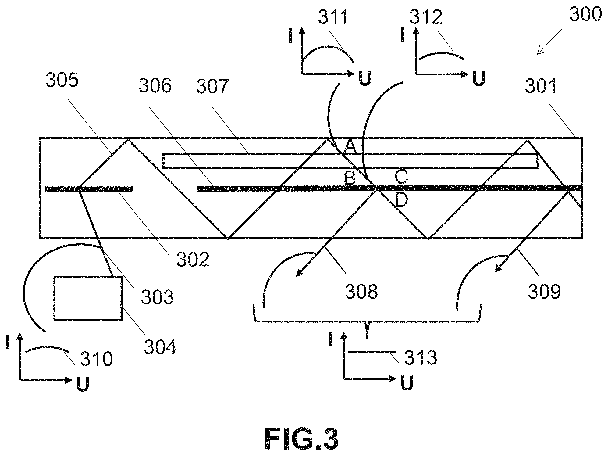
[0101] FIG. 3 conceptually illustrates a waveguide apparatus 300 in which the birefringence control layer and grating provide uniform output illumination in accordance with an embodiment of the invention. In the illustrative embodiment, the waveguide apparatus 300 includes at least one optical substrate 301 and a coupler 302 for deflecting light 303 from an external source 304 into TIR path 305 in the waveguide substrate. The apparatus 300 further includes at least one birefringent grating 306 for providing beam expansion in a first direction and light extraction from the waveguide and at least one birefringence control layer 307 with anisotropic index properties. As shown, light in the TIR ray paths 305 can be diffracted by the output grating into output direction 308, 309. For the purposes of explaining the invention, an initial beam illumination (I) versus angle (U) profile represented by 310 is assumed. The interaction of the light with the birefringence control layer 307 near a grating interaction region along the TIR path 305 is characterized by the illumination profiles before (311) and after (312) propagation through the thickness AB of the birefringence control layer. In some applications, such as but not limited to display applications, the waveguide apparatus 300 can be designed to have uniform illumination versus angle across the exit pupil of the waveguide. This may be achieved by matching the birefringence versus angle characteristics of the birefringence control layer to the angular bandwidth of the grating (along nearby grating paths CD in proximity to the path AB) such that the light extracted by the grating (indicated by 308, 309) integrated across the waveguide exit pupil provides uniform illumination versus angle distribution 313. In some embodiments, the characteristics of the grating and birefringence control layer vary over the aperture of the waveguide.
Implementing Birefringence Control Layers
[0102] Various materials and fabrication processes can be used to provide a birefringence control layer. In many embodiments, the birefringent control layer has anisotropic index properties that can be controlled during fabrication to provide a spatial distribution of birefringence such that the interaction of the light with the birefringence control layer and the birefringent grating integrated along the total internal reflection path for any direction of the light provides a predefined characteristic of the light extracted from the waveguide. In some embodiments, the layer may be implemented as a thin stack that includes more than one layer.
[0103] Alignment of HPDLC gratings can present significant challenges depending on the grating configuration. In the simplest case of a plane grating, polarization control can be confined to a single plane orthogonal to the grating plane. Rolled K-vector gratings can require the alignment to vary across the grating plane. Fold gratings, particularly ones with slanted Bragg fringes, can have much more complicated birefringence, requiring 3D alignment and, in some cases, more highly spatially resolved alignment.
[0104] The following examples of birefringence control layers for use with the invention are illustrative only. In each case, it is assumed that the layer is processed such that the properties vary across the surface of the layer. It is also assumed that the birefringence control layer is configured within the waveguide or on an optical surface of the waveguide containing the grating. In some embodiments, the birefringence control layer is in contact with the grating layer. In several cases, the birefringence control layer spits into separate sections and are disposed on different surfaces of the waveguide. In a number of embodiments, a birefringence layer may include multiple layers.
[0105] In some embodiments, the invention provides a thin polarization control layer that can provide either quarter wave or half wave retardation. The polarization control layer can be implemented as a thin layer directly on top of the grating layer or to one or both of the waveguide substrates using a standard spin coating or ink jet printing process.
[0106] In one group of embodiments, the birefringence control layer is formed using materials using liquid crystal and polymer networks that can be aligned in 3D using directional UV light. In some embodiments, the birefringence control layer is formed at least in part from a Liquid Crystal Polymer (LCP) Network. LCPs, which have also been referred to in the literature as reactive mesogens, are polymerizable liquid crystals containing liquid crystalline monomers that include, for example, reactive acrylate end groups, which polymerize with one another in the presence of photo-initiators and directional UV light to form a rigid network. The mutual polymerization of the ends of the liquid crystal molecules can freeze their orientation into a three-dimensional pattern. The process typically includes coating a material system containing liquid crystal polymer onto a substrate and selectively aligning the LC directors using directionally/spatially controllable UV source prior to annealing. In some embodiments, the birefringence control layer is formed at least in part from a Photo-Alignment Layer, also referred to in the literature as a linearly polymerized photopolymer (LPP). An LPP can be configured to align LC directors parallel or perpendicular to incident linearly polarized UV light. LPP can be formed in very thin layers (typically 50 nm) minimizing the risks of scatter or other spurious optical effect. In some embodiments, the birefringence control layer is formed from LCP, LPP, and at least one dopant. Birefringence control layers based on LCPs and LPPs can be used align LC directors in the complex three-dimensional geometries characteristic of fold gratings and rolled K-vector gratings formed in thin film (2-4 microns). In some embodiments, a birefringence control layer based on LCPs or LPPs further includes dichroic dyes, chiral dopants to achieve narrow or broadband cholesteric filters, twisted retarders, or negative c-plate retarders. In many embodiments, birefringence control layers based on LCPs or LPPs provide quarter or half-wave retardation layers.
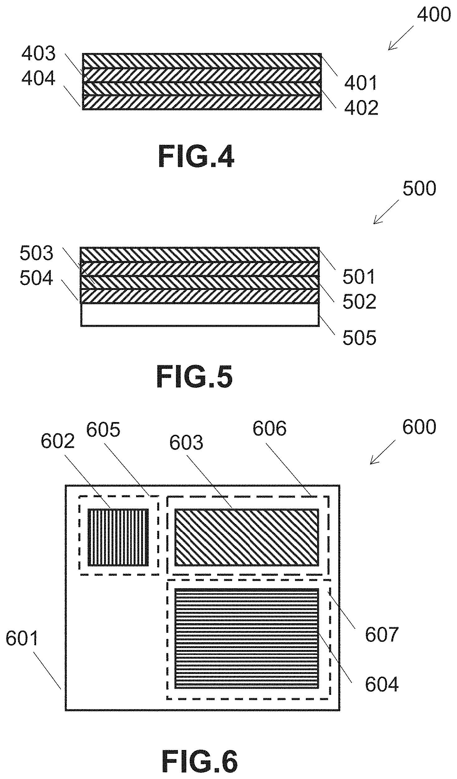
[0107] In some embodiments, the birefringence control layer is formed by a multilayer structure combining isotropic and anisotropic index layers (as shown in FIG. 4). In FIG. 4, the multilayer structure 400 includes isotropic layers 401, 402 and anisotropic index layers 403, 404. In some embodiments, a multiplayer stack may include a high number of layers, such as but not limited to several tens or several hundreds of layers. FIG. 5 conceptually illustrates a multilayer structure 500 that includes isotropic layers 501, 502 and anisotropic index layers 503, 504 combined with a birefringent grating layer 505. When birefringence is on the order of the change of the in-plane refractive index between adjacent material layers of the stack, it is possible to achieved improved control of the reflectivity of P-polarized light. Normally in isotropic materials Brewster's law dictates that for any interface, there is an angle of incidence (Brewster's angle) for which the P-polarization reflectivity vanishes. However, the reflectivity can increase dramatically at other angles. The limitations imposed by the Brewster angle can be overcome by applying the basic principles discussed in Weber et al., "Giant Birefringent Optics in Multilayer Polymer Mirrors," published in Science, Vol. 287, 31 Mar. 2000, pages 2451-2456. Because the optical characteristic of systems of isotropic/anisotropic index layers are based on the fundamental physics of interfacial reflection and phase thickness and not on a particular multilayer interference stack design, new design freedoms are possible. Designs for wide-angle, broadband applications are simplified if the Brewster angle restriction is eliminated, particularly for birefringence control layers immersed in a high-index medium such as a waveguide substrate. A further advantage in relation to waveguide displays is that color fidelity can be maintained for all incidence angles and polarizations.
[0108] A birefringent grating will typically have polarization rotation properties that are functions of angle wavelength. The birefringence control layer can be used to modify the angular, spectral, or polarization characteristics of the waveguide. In some embodiments, the interaction of light with the birefringence control layer can provide an effective angular bandwidth variation along the waveguide. In many embodiments, the interaction of light with the birefringence control layer can provide an effective spectral bandwidth variation along the waveguide. In several embodiments, the interaction of light with the birefringence control layer can provide a polarization rotation along the waveguide. In a number of embodiments, the grating birefringence can be made to vary across the waveguide by spatially varying the composition of the liquid crystal polymer mixture during grating fabrication. In some embodiments, the birefringence control layer can provide a birefringence variation in at least one direction in the plane of the waveguide substrate. The birefringence control layer can also provide a means for optimizing optical transmission (for different polarizations) within the waveguide. In many embodiments, the birefringence control layer can provide a transmission variation in at least one direction in the plane of the waveguide substrate. In several embodiments, the birefringence control layer can provide an angular dependence of at least one of beam transmission or polarization rotation in at least one direction in the plane of the waveguide substrate. In a number of embodiments, the birefringence control layer can provide a spectral dependence of at least one of beam transmission or polarization rotation in at least one direction in the plane of the waveguide substrate.
[0109] In many embodiments, birefringent gratings may provide input couplers, fold gratings, and output gratings in a wide range of waveguide architectures. FIG. 6 conceptually illustrates a plan view of a dual expansion waveguide with birefringent control layers in accordance with an embodiment of the invention. In the illustrative embodiment, the waveguide 600 includes an optical substrate 601 that contains an input grating 602, a fold grating 603, and an output grating 604 that are overlaid by polarization control layers 605, 606, 607, respectively.
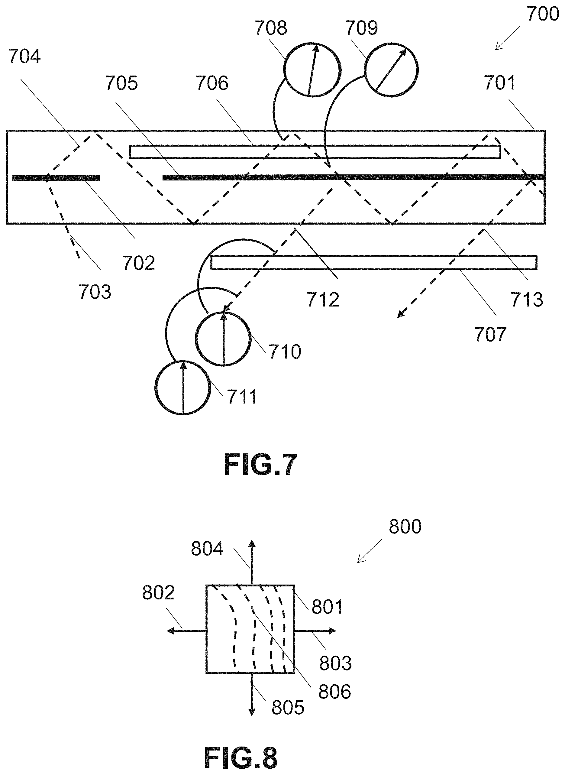
[0110] In some embodiments, the invention provides a polarization-maintaining, wide angle birefringence control layer for modifying the polarization output of a waveguide to balance the birefringence of an external optical element used with the waveguide. FIG. 7 conceptually illustrates an embodiment of the invention directed at automobile HUDs, which reflect collimated imagery off the windscreen into an eyebox. Any windscreen curvature will typically result in aberrations and other geometrical distortion, which cannot be corrected in certain waveguide implementations with the requirement for the beam to remain substantially collimated. One solution to this problem is to mount a correction element, which may be a conventional refractive element or a diffractive element, near the output surface of the waveguide. In such implementations, the birefringence correction component can avoid disturbing ray paths from the waveguide and can be achromatic. The compensator technology used can provide spatially-varying configuration, low haze, and high transmission. In the illustrative embodiment of FIG. 7, the waveguide 700 includes an optical substrate 701 containing a grating coupler 702 for deflecting light 703 from an external source of image modulated light (not shown) into the TIR path 704 in the waveguide, a birefringent grating 705 for providing beam expansion in a first direction and extracting light from the waveguide, and a birefringence control layer 706. The apparatus 700 further includes an optical element 707 disposed in proximity to the waveguide for correcting geometrical distortions and other aberrations introduced by reflection at the windscreen. In some embodiments, the optical element 707 is a refractive lens. In other embodiments, the optical element 707 can be a diffractive lens. For wide field of view HUDs providing a generous eye box, the corrector will typically have a large footprint with a horizontal dimension (along the dashboard) as large as 400 mm. However, if the corrector is molded in plastic, it will tend to suffer from birefringence. Hence, in the embodiment of FIG. 7, the birefringence control element 706 can be designed to compensate for both the grating polarization and polarization rotation introduced by the optical element 707. Referring again to FIG. 7, an initial polarization state corresponding to P polarization is assumed. The polarization state after propagation through the birefringence grating, birefringence control layer, and the correction elements is represented by the symbols 708-711. The interaction of the light with the birefringence control layer near to a grating interaction region along the TIR path is represented by the polarization states. In the embodiment of FIG. 7, the polarization of the light 712, 713 extracted by the grating is aligned parallel to the input polarization vector. In some embodiments, the birefringence control layer 706 may be configured to rotate the output light polarization vector through ninety degrees.
[0111] In some embodiments, the birefringence control layer can be provided by various techniques using mechanical, thermal, or electro-magnetic processing of substrates. For example, in some embodiments, the birefringence control layer is formed by applying spatially varying mechanical stress across the surface of an optical substrate. FIG. 8 conceptually illustrates an apparatus 800 for aligning a birefringence control layer 801 in which forces are applied in the directions indicated by 802-805, resulting in the iso-birefringence contours 806. In many embodiments, the forces illustrated do not necessarily all need to be applied to the layer. In some embodiments, the birefringence control layer 801 is formed by inducing thermal gradients into an optical substrate. In a number of embodiments, the birefringence control layer 801 is provided by a HPDLC grating in which LC directors are aligned using electric or magnetic fields during curing. In several embodiments, two or more of the above techniques may be combined.
Fabrication of Waveguides Implementing Birefringence Control Layers
[0112] The present invention also provides methods and apparatus for fabricating a waveguide containing a birefringent grating and a birefringence control layer. The construction and arrangement of the apparatus and methods as shown in the various exemplary embodiments are illustrative only. Although only a few embodiments have been described in detail in this disclosure, many modifications are possible (for example, additional steps for improving the efficiency of the process and quality of the finished waveguide, minimizing process variances, monitoring the process and others.) Any process step referring to the formation of a layer should be understood to cover multiple such layers. For example, where a process step of recording a grating layer is described, this step can extend to recording a stack containing two or more grating layers. Accordingly, all such modifications are intended to be included within the scope of the present disclosure. The order or sequence of any process or method steps may be varied or re-sequenced according to alternative embodiments. Other substitutions, modifications, changes, and omissions may be made in the design of the process apparatus, operating conditions and arrangement of the exemplary embodiments without departing from the scope of the present disclosure. For the purposes of explaining the invention, the description of the processes will refer to birefringence control layers based on liquid crystal polymer material systems as described above. However, it should be clear from the description that the processes may be based on any of the implementations of a birefringence control layer described herein.
[0113] FIGS. 9A-9F conceptually illustrate the process steps and apparatus for fabricating a waveguide containing a birefringent grating and a birefringence control layer in accordance with various embodiments of the invention. FIG. 9A shows the first step 900 of providing a first transparent substrate 901. FIG. 9B illustrates an apparatus 910 for applying holographic recording material to the substrate 901. In the illustrative embodiment, the apparatus 910 includes a coating apparatus 911 that provides a spray pattern 912 that forms a layer 913 of grating recording material onto the substrate 901. In some embodiments, the spray pattern may include a narrow jet or blade swept or stepped across the surface to be coated. In several embodiments, the spray pattern may include a divergent jet for covering large areas of a surface simultaneously. In a number of embodiments, the coating apparatus may be used in conjunction with one or more masks for providing selective coating of regions of the surface. In many embodiments, the coating apparatus is based on industry-standard standard spin-coating or ink-jet printing processes.
[0114] FIG. 9C conceptually illustrates an apparatus 920 for exposing a layer of grating recording material to form a grating layer in accordance with an embodiment of the invention. In the illustrative embodiment, the apparatus 920 contains a master grating 921 for contact copying the grating in the recording material and a laser 922. As shown, the master 921 diffracts incident light 923 to provide zero order 924 and diffracted light 925, which interferes within the grating material layer to form a grating layer 926. The apparatus may have further features, such as but not limited to light stops and masks for overcoming stray light from higher diffraction orders or other sources. In some embodiments, several gratings may be recorded into a single layer using the principles of multiplexed holograms. FIG. 9D conceptually illustrates an apparatus 930 for coating a layer of liquid crystal polymer material onto the grating layer in accordance with an embodiment of the invention. In the illustrative embodiment, the apparatus 930 contains a coating apparatus 931 configured to deliver a spray pattern 932 forming a layer of material 933. The coating apparatus 931 may have similar features to the coating apparatus used to apply the grating recording material. FIG. 9E conceptually illustrates an apparatus 940 for providing an aligned liquid crystal polymer layer of material in accordance with an embodiment of the invention. In the illustrative embodiment, the apparatus 940 contains a UV source (which can include collimation, beams steering, and beam shaping optics, depending on the specific requirements of a given application) 941 providing directional UV light 942 for forming an aligned LC polymer layer 943. FIG. 9F conceptually illustrates the completed waveguide 950 after the step of applying a second substrate 951 over the aligned liquid crystal polymer layer 943.
[0115] In some embodiments, exposure of the grating recording material may use conventional cross beam recording procedures instead of the mastering process described above. In many embodiments, further processing of the grating layer may include annealing, thermal processing, and/or other processes for stabilizing the optical properties of grating layer. In some embodiments, electrodes coatings may be applied to the substrates. In many embodiments, a protective transparent layer may be applied over the grating layer after exposure. In a number of embodiments, the liquid crystal polymer material is based on the LCP, LPP material systems discussed above. In several embodiments, the alignment of the liquid crystal polymer can result in an alignment of the liquid crystal directors parallel to the UV beam direction. In other embodiments, the alignment is at ninety degrees to the UV beam direction. In some embodiments, the second transparent substrate may be replaced by a protective layer applied using a coating apparatus.
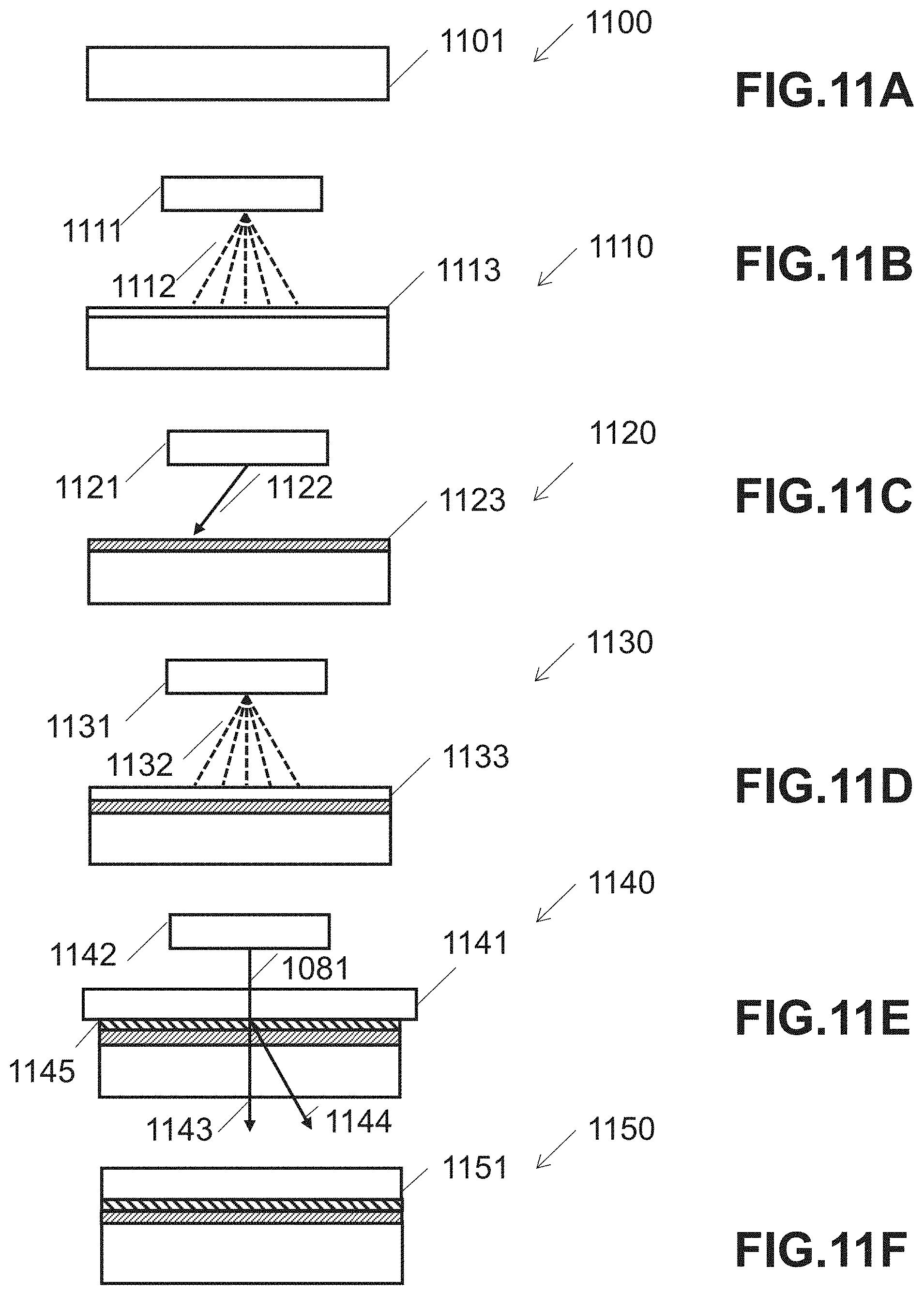
[0116] FIGS. 10A-10F conceptually illustrate the process steps and apparatus for fabricating a waveguide containing a birefringent grating with a birefringence control layer applied to an outer surface of the waveguide in accordance with various embodiments of the invention. FIG. 10A conceptually illustrates the first step 1000 of providing a first transparent substrate 1001 in accordance with an embodiment of the invention. FIG. 10B conceptually illustrates an apparatus 1010 for applying holographic recording material to the substrate in accordance with an embodiment of the invention. In the illustrative embodiment, the apparatus 1010 includes a coating apparatus 1011 providing a spray pattern 1012 that forms the layer 1013 of grating recording material onto the substrate 1001. FIG. 10C conceptually illustrates an apparatus 1020 for exposing a layer of grating recording material to form a grating layer in accordance with an embodiment of the invention. In the illustrative embodiment, the apparatus 1020 includes a master grating 1021 for contact copying the grating in the recording material and a laser 1022. As shown, the master 1021 converts light 1023 from the laser 1022 into zero order 1024 and diffracted light 1025, which interfere within the grating material layer 1013 to form a grating layer 1026. FIG. 10D conceptually illustrates the partially completed waveguide 1030 after the step of applying a second substrate 1031 over the exposed grating layer in accordance with an embodiment of the invention. FIG. 10E conceptually illustrates an apparatus 1040 for coating a layer of liquid crystal polymer material onto the second substrate in accordance with an embodiment of the invention. In the illustrative embodiment, the apparatus 1040 includes a spray coater 1041 for delivering a spray pattern 1042 to form a layer of material 1043. FIG. 10F conceptually illustrates an apparatus 1050 for aligning the liquid crystal polymer material in accordance with an embodiment of the invention. In the illustrative embodiment, the apparatus 1050 includes a UV source 1051 providing the directional UV light 1052 for forming an aligned liquid crystal polymer layer 1053, which can be configured to realign the LC directors of the grating layer 1026.
[0117] FIGS. 11A-11F conceptually illustrate the process steps and apparatus for fabricating a waveguide containing a birefringent grating and a birefringence control layer in accordance with various embodiments of the invention. Unlike the above described embodiments, the step of forming the birefringence control layer can be carried out before the recording of the grating layer, which is formed above the birefringence control layer. FIG. 11A conceptually illustrates the first step 1100 of providing a first transparent substrate 1101. FIG. 11B conceptually illustrates an apparatus 1110 for coating a layer of liquid crystal polymer material onto the first substrate in accordance with an embodiment of the invention. In the illustrative embodiment, the apparatus 1110 includes a coating apparatus 1111 configured to deliver a spray pattern 1112 to form a layer of material 1113. FIG. 11C conceptually illustrates an apparatus 1120 for aligning the liquid crystal polymer material in accordance with an embodiment of the invention. In the illustrative embodiment, the apparatus 1120 includes a UV source 1121 providing the directional UV light 1122 for forming an aligned liquid crystal polymer layer 1123. FIG. 11D conceptually illustrates an apparatus 1130 for applying holographic recording material to the substrate in accordance with an embodiment of the invention. In the illustrative embodiment, the apparatus 1130 includes a coating apparatus 1131 for providing a spray pattern 1132 to form a layer of grating recording material 1133 on top of the liquid crystal polymer layer 1123. FIG. 11E conceptually illustrates an apparatus 1140 for exposing a layer of grating recording material to form a grating layer in accordance with an embodiment of the invention. In the illustrative embodiment, the apparatus 1140 includes a master grating 1141 for contact copying the grating in the recording material and a laser 1142. As shown, the master 1141 converts light 1142 from the laser into zero order 1143 and diffracted light 1144, which interfere in the grating material layer 1133 to form a grating layer 1145, which is aligned by the liquid crystal polymer material layer 1123. FIG. 11F conceptually illustrates the completed waveguide 1150 after the step of applying a second substrate 1151 over the exposed grating layer in accordance with an embodiment of the invention.
[0118] FIG. 12 conceptually illustrates a flow chart illustrating a method of fabricating a waveguide containing a birefringent grating and a birefringence control layer in accordance with an embodiment of the invention. Referring to FIG. 12, the method 1200 includes providing (1201) a first transparent substrate. A layer of grating recording material can be deposited (1202) onto the substrate. The layer of grating recording material can be exposed (1203) to form a grating layer. A layer of liquid crystal polymer material can be deposited (1204) onto the grating layer. The liquid crystal polymer material can be aligned (1205) using directional UV light. A second transparent substrate can be applied (1206) over the alignment layer.
[0119] FIG. 13 conceptually illustrates a flow chart illustrating a method of fabricating a waveguide containing a birefringent grating and a birefringence control layer applied to an outer surface of the waveguide in accordance with an embodiment of the invention. Referring to FIG. 13, the method 1300 includes providing (1301) a first transparent substrate. A layer of grating recording material can be deposited (1302) onto the substrate. The layer of grating recording material can be exposed (1303) to form a grating layer. A second transparent substrate can be applied (1304) over the exposed grating layer. A layer of liquid crystal polymer material can be deposited (1305) onto the second transparent substrate. The liquid crystal polymer material can be aligned (1306) using directional UV light.
[0120] FIG. 14 conceptually illustrates a flow chart illustrating a method of fabricating a waveguide containing a birefringent grating and a birefringence control layer where forming the birefringence control layer is carried out before the recording of the grating layer in accordance with an embodiment of the invention. Referring to FIG. 14, the method 1400 includes providing (1401) a first transparent substrate. A layer of liquid crystal polymer material can be deposited (1402) onto the substrate. The liquid crystal polymer material can be aligned (1403) using directional UV light. A layer of grating recording material can be deposited (1404) onto the aligned liquid crystal polymer material. The layer of grating recording material can be exposed (1405) to form a grating layer. A second transparent substrate can be applied (1406) over the grating layer.
[0121] Although FIGS. 12-14 illustrate specific processes for fabricating waveguides containing a birefringent grating and a birefringence control layer, many other fabrication processes and apparatus can be implemented to form such waveguides in accordance with various embodiments of the invention. For example, the order or sequence of any process or method steps may be varied or re-sequenced according to alternative embodiments. Other substitutions, modifications, changes, and omissions may be made in the design of the process apparatus, operating conditions and arrangement of the exemplary embodiments without departing from the scope of the present disclosure.
Additional Embodiments and Applications
[0122] In some embodiments, a polarization-maintaining, wide angle, high reflection waveguide cladding with polarization compensation for grating birefringence can be implemented. FIG. 15 shows one such embodiment. In the illustrative embodiment, the waveguide 1500 includes a waveguiding substrate 1501 containing a birefringent grating 1502 and a birefringence control layer 1503 overlaying the waveguiding substrate 1501. As shown, guided light 1504 interacting with the birefringence control layer 1503 at its interface with the waveguiding substrate 1501 has its polarization rotated from the state indicated by symbol 1505 (resulting from the previous interaction with the grating) to the state indicated by 1506 (which has a desired orientation for the next interaction with the grating, for example, having an orientation for providing a predefined diffraction efficiency at some pre-defined point along the grating).
[0123] In many embodiments, a compact and efficient birefringence control layer for isolating a waveguide from its environment while ensuring efficient confinement of wave-guided beams can be implemented. FIG. 16 illustrates one such embodiment. In the illustrative embodiment, the environmentally isolated waveguide 1600 includes a waveguiding substrate 1601 containing a birefringent grating 1602 and a birefringence control layer 1603 overlaying the waveguiding substrate 1601. As shown, guided light 1604 interacting with the birefringence control layer 1603 at its interface with the waveguiding substrate 1601 has its polarization rotated from the state indicated by the symbol 1605 to the state indicated by 1606. Environmental isolation of the waveguide can be provided by designing the birefringence control layer 1603 such that total internal reflection occurs at the interface 1607 between the birefringence control layer 1603 and the waveguiding substrate 1601. In some embodiments, environmental isolation is provided by designing the birefringence control layer to have gradient index characteristics such that only a small portion of the guided light is reflected at the air interface of the birefringence control layer. In several embodiments, the birefringence control layer may incorporate a separate GRIN layer. In a number of embodiments, a GRIN layer may be based on embodiments disclosed in U.S. Provisional Patent Application No. 62/123,282 entitled NEAR EYE DISPLAY USING GRADIENT INDEX OPTICS and U.S. Provisional Patent Application No. 62/124,550 entitled WAVEGUIDE DISPLAY USING GRADIENT INDEX OPTICS.
[0124] FIG. 17 conceptually illustrates an apparatus 1700, which may be used in conjunction with some of the methods described above, for fabricating a structure containing a birefringent grating layer 1701 overlaying a birefringence control layer 1702 in accordance with an embodiment of the invention. In FIG. 17, the substrate supporting the birefringence control layer is not shown. The construction beams, indicated by rays 1703, 1704, may be provided by a master grating or a crossed beam holographic recording setup. As shown, the construction beams propagate through the birefringence control layer 1702. In many embodiments, the construction beams are in the visible band. In some embodiments, the construction beams are in the UV band.
[0125] FIG. 18 conceptually illustrates an apparatus 1800, which may be used in conjunction with some of the methods described above, for fabricating a structure containing a birefringence control layer 1801 overlaying a birefringent grating layer 1802 in accordance with an embodiment of the invention. In FIG. 18, the substrate supporting the grating layer is not shown. The direction of a recording beam is indicated by 1803. In many embodiments the birefringence control layer is a liquid crystal polymer material system which uses a directional UV beam for alignment. In some embodiments, in which the grating is a recorded in a polymer and liquid crystal material system, an exposed grating may be erased during the process of aligning the birefringence control layer by applying an external stimulus such as heat, electric or magnetic fields or light to effective to create an isotropic phase of the liquid crystal.
[0126] FIG. 19 conceptually illustrates a cross section of waveguide 1900 containing substrates 1901, 1902 sandwiching a grating layer 1903. As shown, a source 1904 emits collimated light 1905A, which is coupled by the grating layer into the total internal reflection (TIR) path indicated by rays 1905B, 1905C and extracted by the grating layer 1903 into the output ray path 1905D. In the illustrative embodiments, the source 1904 can be a variety of light sources, including but not limited to a laser or a LED.
[0127] FIG. 20 conceptually illustrates a waveguide similar to the one of FIG. 19 with a quarter wave polarization layer inserted by replacing the substrate 1902 by a quarter wave film 2001 sandwiched by substrates 2002, 2003 in accordance with an embodiment of the invention. A quarter wave polarization layer can be beneficial to the holographic waveguide design in two ways. Firstly, it can reduce reinteraction (outcoupling) of a rolled K-vector (RKV) input grating to increase the overall coupling efficiency of the input grating. Secondly, it can continuously mix up the polarization of the light going into the fold and output gratings to provide better extraction. The quarter wave layer can be located on a waveguide surface along the optical from the input grating. Typically, a waveguide surface can include one of the TIR surface of the wave or some intermediate surface formed inside the waveguide. The optical characteristics of the quarter wave layer can be optimized for "waveguide angles"--i.e., angles in glass beyond the TIR angle. In some embodiments, the center field is designed at approximately 55 deg. in glass (corresponding to a refractive index of approximately 1.51 at wavelength 532 nm). In many embodiments, optimization for red, green, and blue can be used for optimum performance of red, green, and blue transmitting waveguides. As will be shown in the embodiments to be described, there are several different ways of incorporating the quarter wave film within a waveguide. In the following embodiment, we refer generally to a quarter wave polarization layer provided by a liquid crystal polymer (LCP) material. However, it should be understood that other materials be used in applications of the invention.
[0128] FIG. 21 conceptually illustrates a schematic cross section view 2100 showing a portion of a waveguide illustrating how the use of a quarter wave polarization layer with a RKV grating can overcome the problem of unwanted extraction of light along the propagation path in the input grating portion of the waveguide in accordance with an embodiment of the invention. One ray path is illustrated in which input light including the P-polarized light 2101A is coupled by the grating layer into a TIR path indicated by the rays 2101B-2101L in the waveguide. The waveguide grating has rolled K-vectors of which examples occurring at three points along the length of the waveguide are illustrated schematically by the vectors 2102A-2102C. In the illustrative embodiment, the light 2101A diffractively coupled into TIR by the input grating is P-polarized with respect to the grating. In many embodiments, the TIR angle can be nominally 55 degrees in glass. On transmission through the quarter wave layer, the polarization of the light changes from P to circularly polarized (2101C). After TIR at the lower surface of the waveguide the polarization changes to circularly polarized light (2101D) of an opposing sense such that after traversing the quarter wave layer on its upward path becomes S-polarized (2101E) with respect to the grating. The S-polarized light passes through the gating without deviation (2101F) or substantial loss since it is both off-Bragg and "off polarization" (since the grating has zero or low diffraction efficiency for S). This light then undergoes TIR (2101G) a second time retaining its S-polarization. Hence the light 2101G is now on-Bragg but is still off polarization with respect to the P-polarization sensitive grating. The light therefore passes through the grating without diffraction (2101H). At this location the RKV (2102B) has rolled slightly from the one (2102A) near the light entry point on the UP grating. If the light was "on polarization," the `roll` effect of RKV would be small, and so the light would be strongly out-coupled. The S-polarization light passing through the grating goes through another full cycle, (2101H-2101M) in a similar fashion to the cycle illustrated by rays 2101B-2101G, and then returns to a P-polarized state for the next (2101M) on-Bragg interaction at the grating region with K-vector 2102C. At this point, the light has performed two complete TIR bounce cycles down the waveguide, increasing the angular separation of the incidence angle at the grating and K-vector, which strongly reduces the on-Bragg interaction.
[0129] To clarify the embodiment of FIG. 21 further, a 55-degree TIR angle light in a 1 mm thick waveguide is considered, with a 20 mm projector relief (distance of the projector from the input grating), and a nominal 4.3 mm diameter projector exit pupil: The first interaction with the grating takes place approximately 2.85 mm down the waveguide. This equates to an 8.1-degree angle at 20 mm projector relief. For comparison the FWHM angular bandwidth of a typical 1.6 um grating is about 12 degrees in air (prescription dependent) i.e. the angle subtended by the pupil is not much larger than the semi-width of the lens. This leads to strong outcoupling if polarization is not changed to S-polarized as described above. In effect, the use of the quarter wave layer doubles the TIR length to approximately 5.7 mm. This offset equates to about 15.9 deg, which is larger than the angular bandwidth of most waveguide gratings, thereby reducing outcoupling reinteraction losses from the waveguide.
[0130] FIG. 22 conceptually illustrates a polarization layer architecture 2200 containing an LCP quarter wave cell and a reactive monomer liquid crystal mixture (RMLCM) cell separated by index matching oil layer (2201) in accordance with an embodiment of the invention. The LCP cell includes a substrate 2202 and the LCP film 2203. The RMLCM cell includes substrates 2204, 2205 sandwiching the RMLCM layer 2206. This configuration has the advantage that the index matching oil bond can provide a non-permanent bond, which allows for installation and removal of polarization cell for testing purposes. Adhesive can also be applied at the edges (tacked) for a semi-permanent bond. In some embodiments the oil layer can be provided using a cell filled with oil.
[0131] FIG. 23 conceptually illustrates an example of a polarization architecture 2300 based on a grating cell with the RMLCM grating material layer 2301 in direct contact with a bare LCP film 2302 in accordance with an embodiment of the invention. The two films are sandwiched by the substrates 2303, 2304. This is a simple and cost-effective solution for implementing an LCP layer. Maintaining thickness control of the RMLCM layer using spacer beads can be difficult if the beads are embedded directly onto LCP layer. The embodiment of FIG. 23 can required careful matching of the material properties of the RMLCM and LCP to avoid detrimental interactions between the RMLCM and the LCP layers. In many embodiments, holographic exposure of the RMLCM layer can be applied directly into the RMLCM and does not need to be through the LCP layer. If exposure construction through the LCP layer is unavoidable, pre-compensation of polarization rotation of the LCP layer can be made in some embodiments.
[0132] FIG. 24 conceptually illustrates a cross section view schematically showing an example of polarization layer architecture 2400 in which a bare LCP layer is bonded to a bare RMLCM layer in accordance with an embodiment of the invention. The apparatus includes an upper substrate 2401, a bare LCP film 2402, adhesive layer 2403, an exposed RMLCM layer 2404, and a lower substrate 2405. In many embodiments, the adhesive layer can be Norland NOA65 adhesive or a similar adhesive.
[0133] FIG. 25 conceptually illustrates a cross section view schematically showing an example of a polarization layer architecture 2500 using a RMLCM layer as a polarization layer in accordance with an embodiment of the invention. The apparatus includes an upper substrate 2501, an upper RMLCM layer 2502, a transparent spacer 2503, a lower RMLCM layer 2504, and a lower substrate 2505. One of the RMLCM layers can be used not only as the grating material, but also as a polarization rotation layer, using the inherent birefringent properties of RMLCM materials. The `polarization rotation grating` should have a period and/or k-vector direction such that its diffraction is minimal. In some embodiments the RMLCM layer can be configure as a subwavelength grating. In some embodiments, the RMCM layer can be provided sandwiched between two release layers such that after curing the layer can be removed and re-applied elsewhere.
[0134] FIG. 26 conceptually illustrates an example of a polarization layer architecture 2600 that includes a feature for compensating for polarization rotation introduced by birefringent gratings in accordance with an embodiment of the invention. The apparatus includes an upper substrate 2601, a polarization control layer 2602, a transparent substrate 2603, a grating layer 2604, and a lower substrate 2605. The grating layer contains a first grating 2606A and a second grating 2606B separated by a clear region 2607. In some embodiments, the clear region can a polymer with refractive index similar to that of the substrates. In many embodiments other low refractive index materials may be used to provide the clear region. The polarization control layer includes quarter wave retarding regions 2608A, 2608B and a polarization compensation region, which balances the polarization rotation introduced by the birefringent grating 2606A (in the case where the guide light propagates from grating 2606A to grating 2606B).
[0135] FIG. 27 conceptually illustrates a plan view schematically showing a waveguide display 2700 incorporating the features of the embodiment of FIG. 26 in accordance with an embodiment of the invention. The waveguide display 2700 includes a waveguide substrate 2701, an input grating 2702, a fold grating 2703, and an output grating 2704. Polarization control regions 2705, 2706 apply compensation for grating depolarization according to the principle of the embodiment of FIG. 26.
[0136] FIG. 28 conceptually illustrates a cross section view schematically showing an example of a polarization layer architecture 2800 containing an upper substrate 2801, an LCP layer 2802 with hard encapsulation layer 2803, a RMLCM layer 2804, and a lower substrate 2805 in accordance with an embodiment of the invention. In many embodiments, the hard encapsulation layer or film can be designed to protect the delicate LCP film from mechanical contact, such that standard cleaning procedures will not destroy the film. Advantageously, the hard encapsulation layer can employ a material resistant to spacer beads being pushed into it through the lamination process, as well as being chemically resistant to index matching oil and adhesives.
[0137] FIG. 29 conceptually illustrates a cross section view schematically showing an example of a polarization layer architecture 2900 containing an upper substrate 2901, an LCP layer 2902 with soft encapsulation layer 2903, a RMLCM layer 2904, and a lower substrate 2905 in accordance with an embodiment of the invention. The polarization alignment film can be encapsulated with a soft encapsulation layer or film designed to protect the delicate LCP film from mechanical contact, such that standard cleaning procedures such as drag wiping with iso-propyl alcohol, for example, will not destroy the film. In some embodiments, the soft encapsulation can provide some resistance to spacer beads during the lamination process.
[0138] FIG. 30 conceptually illustrates a plan view schematically showing a first example 3000 of a two-region polymer film in accordance with an embodiment of the invention. This example using a non-encapsulated LCP film 3001 supported by a 0.5 mm thickness Eagle XG substrate of dimensions 77.2 mm.times.47.2 mm. Region 1 is characterized by a fast axis 75.degree. from horizontal and by quarter-wave retardance at 55.degree. in-glass angle, 45.degree. ellipticity .+-.5.degree., for wavelength 524 nm. Region 2 is characterized by a fast axis 105.degree. from horizontal and a quarter-wave retardance at 55.degree. in-glass angle, 45.degree. ellipticity .+-.5.degree., for wavelength 524 nm. Typically, region 1 and region 2 extend to the halfway point horizontally, .+-.2 mm.
[0139] FIG. 31 conceptually illustrates a plan view schematically showing a second example 3100 of a two-region polymer film in accordance with an embodiment of the invention. This example uses encapsulation of the LCP layer 3101 by a protective film 3102, said layers supported by a 0.5 mm thickness Eagle XG substrate of dimensions 77.2 mm.times.47.2 mm. Region 1 is characterized by a fast axis 75.degree. from horizontal and by quarter-wave retardance at 55.degree. in-glass angle, 45.degree. ellipticity .+-.5.degree., for wavelength 524 nm. Region 2 is characterized by a fast axis 105.degree. from horizontal and by quarter-wave retardance at 55.degree. in-glass angle, 45.degree. ellipticity .+-.5.degree., for wavelength 524 nm. Typically, Region 1 and region 2 extend to the halfway point horizontally, .+-.2 mm. The encapsulation layer can seal the polarization layer such that performance is unaffected when covered by layer of oil such as Cargille Series A with refractive index 1.516. The encapsulation layer can seal the polarization layer such that performance is unaffected when covered by an additional layer of liquid crystal-based photopolymer.
[0140] FIG. 32 conceptually illustrates a plan view schematically showing a third example 3200 of a two-region polymer film in accordance with an embodiment of the invention. This example uses glass encapsulation of the LCP. A 0.5 mm thickness Eagle XG substrate of dimensions 77.2 mm.times.47.2 mm supports a LCP layer 3201, an adhesive layer 3202, and 0.2 mm thickness Willow glass cover 3203. Region 1 is characterized by a fast axis 75.degree. from horizontal and by quarter-wave retardance at 55.degree. in-glass angle, 45.degree. ellipticity .+-.5.degree., for wavelength 524 nm. Region 2 is characterized by a fast axis 105.degree. from horizontal and by a quarter-wave retardance at 55.degree. in-glass angle, 45.degree. ellipticity .+-.5.degree., for wavelength 524 nm. Advantageously, the glass for encapsulations of the LCP is 0.5 mm EagleXG or 0.2 mm Willow glass. Typically, Region 1 and region 2 extend to the halfway point horizontally, .+-.2 mm.
[0141] FIG. 33 conceptually illustrates a drawing showing the clear aperture layout 3300 for the embodiments illustrated in FIGS. 30-32 in accordance with an embodiment of the invention. The clear aperture is highlighted in the dashed line. All dimensions are in mm.
[0142] FIG. 34 conceptually illustrates a plan view 3400 schematically showing the waveguide 3401 containing input 3402, fold 3403, and output 3404 gratings based on the embodiments of FIGS. 30-33, including the K-vectors and alignment layer fast axis directions for each grating in accordance with an embodiment of the invention. As shown in FIG. 34, the K-vector and fast axis directions are for the input grating K-vector: 30 degrees; for the fold grating K-vector: 270 degrees; and for the output grating K-vector: 150 degrees.
[0143] The above description covers only some of the possible embodiments in which an LCP layer (or equivalent retarding layer) can be combined with an RMLCM layer in a waveguide structure. In many of the above described embodiments, the substrates can be fabricated from 0.5 mm thickness Corning Eagle XG glass. In some embodiments, thinner or thicker substrates can be used. In several embodiments, the substrates can be fabricated from plastic. In a number of embodiments, the substrates and optical layers encapsulated by the said substrates can be curved. Any of the embodiments can incorporated additional layers for protection from chemical contamination or damage incurred during processing and handling. In some embodiments, additional substrate layers may be provided to achieve a required waveguide thickness. In some embodiments, additional layers may be provided to perform at least one of the functions of illumination homogenization spectral filtering, angle selective filtering, stray light control, and debanding. In many embodiments, the bare LCP layer can be bonded directly to a bare exposed RMLCM layer. In several embodiments, an intermediate substrate can be disposed between the LCP layer and the RMLCM layer. In a number of embodiments, the LCP layer can be combined with an unexposed layer of RMLCM material. In many embodiments, layers of LCP, with or without encapsulation, can have haze characteristics <0.25%, and preferably 0.1% or less. It should be noted that the quoted haze characteristics are based on bulk material scatter and are independent of surface scatter losses, which are largely lost upon immersion. The LCP and encapsulation layers can survive 100 C exposure (>80 C for thermal UM exposures). In many embodiments, the LCP encapsulation layer can be drag wipe resistant to permit layer cleaning. In the embodiments described above, there can be constant retardance and no bubbles or voids within the film clear aperture. The LCP and adhesive layers can match the optical flatness criteria met by the waveguide substrates.
[0144] A color waveguide according to the principles of the invention would typically include a stack of monochrome waveguides. The design may use red, green, and blue waveguide layers or, alternatively, red and blue/green layers. In some embodiments, the gratings are all passive, that is non-switching. In some embodiments, at least one of the gratings is switching. In some embodiments, the input gratings in each layer are switchable to avoid color crosstalk between the waveguide layers. In some embodiments color crosstalk is avoided by disposing dichroic filters between the input grating regions of the red and blue and the blue and green waveguides. In some embodiments, the thickness of the birefringence control layer is optimized for the wavelengths of light propagating within the waveguide to provide the uniform birefringence compensation across the spectral bandwidth of the waveguide display. Wavelengths and spectral bandwidths bands for red, green, blue wavelengths typically used in waveguide displays are red: 626 nm.+-.9 nm, green: 522 nm.+-.18 nm and blue: 452 nm.+-.11 nm. In some embodiments, the thickness of the birefringence control layer is optimized for trichromatic light.
[0145] In many embodiments, the birefringence control layer is provided by a subwavelength grating recorded in HPDLC. Such gratings are known to exhibit the phenomenon of form birefringence and can be configured to provide a range of polarization functions including quarter wave and half wave retardation. In some embodiments, the birefringence control layer is provided by a liquid crystal medium in which the LC directors are aligned by illuminating an azo-dye doped alignment layer with polarized or unpolarized light. In a number of embodiments, a birefringence control layer is patterned to provide LC director orientation patterns with submicron resolution steps. In same embodiments, the birefringence control layer is processed to provide continuous variation of the LC director orientations. In several embodiments, a birefringence control layer provided by combining one or more of the techniques described above is combined with a rubbing process or a polyimide alignment layer. In some embodiments, the birefringence control layer provides optical power. In a number of embodiments, the birefringence control layer provides a gradient index structure. In several embodiments, the birefringence control layer is provided by a stack containing at least one HPDLC grating and at least one alignment layer. In many embodiments, the birefringent grating may have rolled k-vectors. The K-vector is a vector aligned normal to the grating planes (or fringes) which determines the optical efficiency for a given range of input and diffracted angles. Rolling the K-vectors allows the angular bandwidth of the grating to be expanded without the need to increase the waveguide thickness. In many embodiments, the birefringent grating is a fold grating for providing exit pupil expansion. The fold grating may be based on any of the embodiments disclosed in PCT Application No.: PCT/GB2016000181 entitled WAVEGUIDE DISPLAY and embodiments discussed in the other references give above.
[0146] In some embodiments, the apparatus is used in a waveguide design to overcome the problem of laser banding. A waveguide according to the principles of the invention can provide a pupil shifting means for configuring the light coupled into the waveguide such that the input grating has an effective input aperture which is a function of the TIR angle. Several embodiments of the pupil shifting means will be described. The effect of the pupil shifting means is that successive light extractions from the waveguide by the output grating integrate to provide a substantially flat illumination profile for any light incidence angle at the input grating. The pupil shifting means can be implemented using the birefringence control layers to vary at least one of amplitude, polarization, phase, and wavefront displacement in 3D space as a function of incidence light angle. In each case, the effect is to provide an effective aperture that gives uniform extraction across the output grating for any light incidence angle at the input grating. In some embodiments, the pupil shifting means is provided at least in part by designing the optics of the input image generator to have a numerical aperture (NA) variation ranging from high NA on one side of the microdisplay panel varying smoothly to a low NA at the other side according to various embodiments, such as those similar to ones disclosed in PCT Application No.: PCT/GB2016000181 entitled WAVEGUIDE DISPLAY, the disclosure of which is hereby incorporated in its entirety. Typically, the microdisplay is a reflective device.
[0147] In some embodiments, the grating layer may be broken up into separate layers. The number of layers may then be laminated together into a single waveguide substrate. In many embodiments, the grating layer contains several pieces, including the input coupler, the fold grating, and the output grating (or portions thereof) that are laminated together to form a single substrate waveguide. The pieces may be separated by optical glue or other transparent material of refractive index matching that of the pieces. In several embodiments, the grating layer may be formed via a cell making process by creating cells of the desired grating thickness and vacuum filling each cell with SBG material for each of the input coupler, the fold grating and the output grating. In one embodiment, the cell is formed by positioning multiple plates of glass with gaps between the plates of glass that define the desired grating thickness for the input coupler, the fold grating and the output grating. In one embodiment, one cell may be made with multiple apertures such that the separate apertures are filled with different pockets of SBG material. Any intervening spaces may then be separated by a separating material (e.g., glue, oil, etc.) to define separate areas. In one embodiment, the SBG material may be spin-coated onto a substrate and then covered by a second substrate after curing of the material. By using a fold grating, the waveguide display advantageously requires fewer layers than previous systems and methods of displaying information according to some embodiments. In addition, by using a fold grating, light can travel by total internal refection within the waveguide in a single rectangular prism defined by the waveguide outer surfaces while achieving dual pupil expansion. In another embodiment, the input coupler, the gratings can be created by interfering two waves of light at an angle within the substrate to create a holographic wave front, thereby creating light and dark fringes that are set in the waveguide substrate at a desired angle. In some embodiments, the grating in a given layer is recorded in stepwise fashion by scanning or stepping the recording laser beams across the grating area. In some embodiments, the gratings are recorded using mastering and contact copying process currently used in the holographic printing industry.
[0148] In many embodiments, the gratings are Bragg gratings recorded in holographic polymer dispersed liquid crystal (HPDLC) as already discussed, although SBGs may also be recorded in other materials. In one embodiment, SBGs are recorded in a uniform modulation material, such as POLICRYPS or POLIPHEM having a matrix of solid liquid crystals dispersed in a liquid polymer. The SBGs can be switching or non-switching in nature. In its non-switching form a SBG has the advantage over conventional holographic photopolymer materials of being capable of providing high refractive index modulation due to its liquid crystal component. Exemplary uniform modulation liquid crystal-polymer material systems are disclosed in United State Patent Application Publication No.: US2007/0019152 by Caputo et al and PCT Application No.: PCT/EP2005/006950 by Stumpe et al., both of which are incorporated herein by reference in their entireties. Uniform modulation gratings are characterized by high refractive index modulation (and hence high diffraction efficiency) and low scatter. In some embodiments at least one of the gratings is a surface relief grating. In some embodiments at least one of the gratings is a thin (or Raman-Nath) hologram,
[0149] In some embodiments, the gratings are recorded in a reverse mode HPDLC material. Reverse mode HPDLC differs from conventional HPDLC in that the grating is passive when no electric field is applied and becomes diffractive in the presence of an electric field. The reverse mode HPDLC may be based on any of the recipes and processes disclosed in PCT Application No.: PCT/GB2012/000680, entitled IMPROVEMENTS TO HOLOGRAPHIC POLYMER DISPERSED LIQUID CRYSTAL MATERIALS AND DEVICES. The grating may be recorded in any of the above material systems but used in a passive (non-switching) mode. The fabrication process can be identical to that used for switched but with the electrode coating stage being omitted. LC polymer material systems may be used for their high index modulation. In some embodiments, the gratings are recorded in HPDLC but are not switched.
[0150] In many embodiments, a waveguide display according to the principles of the invention may be integrated within a window, for example, a windscreen-integrated HUD for road vehicle applications. In some embodiments, a window-integrated display may be based on the embodiments and teachings disclosed in U.S. Provisional Patent Application No. 62/125,064 entitled OPTICAL WAVEGUIDE DISPLAYS FOR INTEGRATION IN WINDOWS and U.S. patent application Ser. No. 15/543,016 entitled ENVIRONMENTALLY ISOLATED WAVEGUIDE DISPLAY. In some embodiments, a waveguide display according to the principles of the invention may incorporate a light pipe for providing beam expansion in one direction based on the embodiments disclosed in U.S. patent application Ser. No. 15/558,409 entitled WAVEGUIDE DEVICE INCORPORATING A LIGHT PIPE. In some embodiments, the input image generator may be based on a laser scanner as disclosed in U.S. Pat. No. 9,075,184 entitled COMPACT EDGE ILLUMINATED DIFFRACTIVE DISPLAY. The embodiments of the invention may be used in wide range of displays including HMDs for AR and VR, helmet mounted displays, projection displays, heads up displays (HUDs), Heads Down Displays, (HDDs), autostereoscopic displays and other 3D displays. Some of the embodiments and teachings of this disclosure may be applied in waveguide sensors such as, for example, eye trackers, fingerprint scanners and LIDAR systems and in illuminators and backlights.
[0151] It should be emphasized that the drawings are exemplary and that the dimensions have been exaggerated. For example, thicknesses of the SBG layers have been greatly exaggerated. Optical devices based on any of the above-described embodiments may be implemented using plastic substrates using the materials and processes disclosed in PCT Application No.: PCT/GB2012/000680, entitled IMPROVEMENTS TO HOLOGRAPHIC POLYMER DISPERSED LIQUID CRYSTAL MATERIALS AND DEVICES. In some embodiments, the dual expansion waveguide display may be curved.
[0152] Although the description has provided specific embodiments of the invention, additional information concerning the technology may be found in the following patent applications, which are incorporated by reference herein in their entireties: U.S. Pat. No. 9,075,184 entitled COMPACT EDGE ILLUMINATED DIFFRACTIVE DISPLAY, U.S. Pat. No. 8,233,204 entitled OPTICAL DISPLAYS, PCT Application No.: US2006/043938, entitled METHOD AND APPARATUS FOR PROVIDING A TRANSPARENT DISPLAY, PCT Application No.: GB2012/000677 entitled WEARABLE DATA DISPLAY, U.S. patent application Ser. No. 13/317,468 entitled COMPACT EDGE ILLUMINATED EYEGLASS DISPLAY, U.S. patent application Ser. No. 13/869,866 entitled HOLOGRAPHIC WIDE ANGLE DISPLAY, and U.S. patent application Ser. No. 13/844,456 entitled TRANSPARENT WAVEGUIDE DISPLAY, U.S. patent application Ser. No. 14/620,969 entitled WAVEGUIDE GRATING DEVICE, U.S. patent application Ser. No. 15/553,120 entitled ELECTRICALLY FOCUS TUNABLE LENS, U.S. patent application Ser. No. 15/558,409 entitled WAVEGUIDE DEVICE INCORPORATING A LIGHT PIPE, U.S. patent application Ser. No. 15/512,500 entitled METHOD AND APPARATUS FOR GENERATING INPUT IMAGES FOR HOLOGRAPHIC WAVEGUIDE DISPLAYS, U.S. Provisional Patent Application No. 62/123,282 entitled NEAR EYE DISPLAY USING GRADIENT INDEX OPTICS, U.S. Provisional Patent Application No. 62/124,550 entitled WAVEGUIDE DISPLAY USING GRADIENT INDEX OPTICS, U.S. Provisional Patent Application No. 62/125,064 entitled OPTICAL WAVEGUIDE DISPLAYS FOR INTEGRATION IN WINDOWS, U.S. patent application Ser. No. 15/543,016 entitled ENVIRONMENTALLY ISOLATED WAVEGUIDE DISPLAY, U.S. Provisional Patent Application No. 62/125,089 entitled HOLOGRAPHIC WAVEGUIDE LIGHT FIELD DISPLAYS, U.S. Pat. No. 8,224,133 entitled LASER ILLUMINATION DEVICE, U.S. Pat. No. 8,565,560 entitled LASER ILLUMINATION DEVICE, U.S. Pat. No. 6,115,152 entitled HOLOGRAPHIC ILLUMINATION SYSTEM, PCT Application No.: PCT/GB2013/000005 entitled CONTACT IMAGE SENSOR USING SWITCHABLE BRAGG GRATINGS, PCT Application No.: PCT/GB2012/000680, entitled IMPROVEMENTS TO HOLOGRAPHIC POLYMER DISPERSED LIQUID CRYSTAL MATERIALS AND DEVICES, PCT Application No.: PCT/GB2014/000197 entitled HOLOGRAPHIC WAVEGUIDE EYE TRACKER, PCT/GB2013/000210 entitled APPARATUS FOR EYE TRACKING, PCT Application No.: GB2013/000210 entitled APPARATUS FOR EYE TRACKING, PCT/GB2015/000274 entitled HOLOGRAPHIC WAVEGUIDE OPTICALTRACKER, U.S. Pat. No. 8,903,207 entitled SYSTEM AND METHOD OF EXTENDING VERTICAL FIELD OF VIEW IN HEAD UP DISPLAY USING A WAVEGUIDE COMBINER, U.S. Pat. No. 8,639,072 entitled COMPACT WEARABLE DISPLAY, U.S. Pat. No. 8,885,112 entitled COMPACT HOLOGRAPHIC EDGE ILLUMINATED EYEGLASS DISPLAY, U.S. patent application Ser. No. 16/086,578 entitled METHOD AND APPARATUS FOR PROVIDING A POLARIZATION SELECTIVE HOLOGRAPHIC WAVEGUIDE DEVICE, U.S. Provisional Patent Application No. 62/493,578 entitled WAVEGUIDE DISPLAY APPARATUS, PCT Application No.: PCT/GB2016000181 entitled WAVEGUIDE DISPLAY, U.S. Patent Application No. 62/497,781 entitled APPARATUS FOR HOMOGENIZING THE OUTPUT FROM A WAVEGUIDE DEVICE, U.S. Patent Application No. 62/499,423 entitled WAVEGUIDE DEVICE WITH UNIFORM OUTPUT ILLUMINATION.
Doctrine of Equivalents
[0153] The construction and arrangement of the systems and methods as shown in the various exemplary embodiments are illustrative only. Although only a few embodiments have been described in detail in this disclosure, many modifications are possible (for example, variations in sizes, dimensions, structures, shapes and proportions of the various elements, values of parameters, mounting arrangements, use of materials, colors, orientations, etc.). For example, the position of elements may be reversed or otherwise varied, and the nature or number of discrete elements or positions may be altered or varied. Accordingly, all such modifications are intended to be included within the scope of the present disclosure. The order or sequence of any process or method steps may be varied or re-sequenced according to alternative embodiments. Other substitutions, modifications, changes, and omissions may be made in the design, operating conditions and arrangement of the exemplary embodiments without departing from the scope of the present disclosure.
* * * * *
D00000
D00001
D00002
D00003
D00004
D00005
D00006
D00007
D00008
D00009
D00010
D00011
D00012

D00013
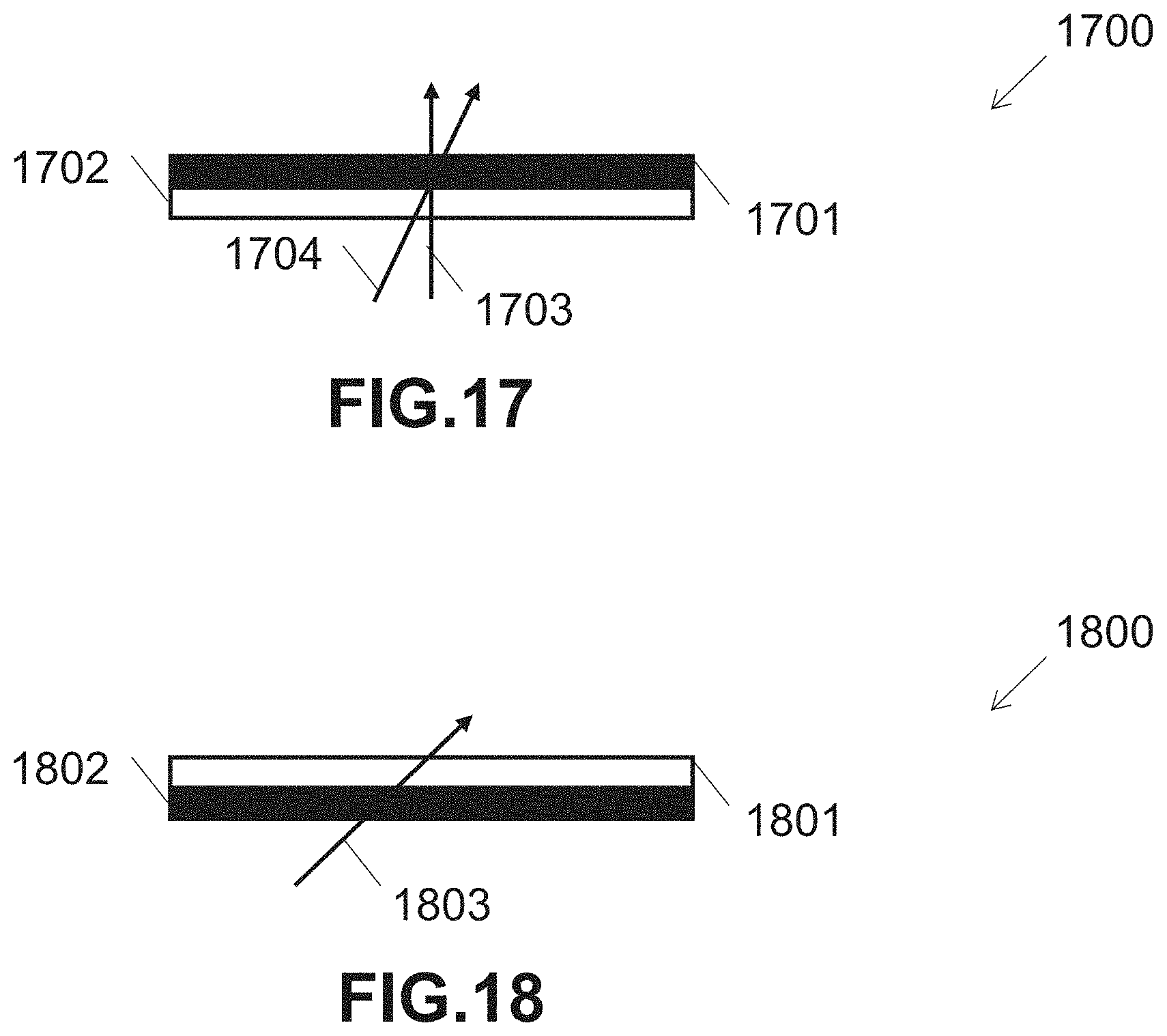
D00014
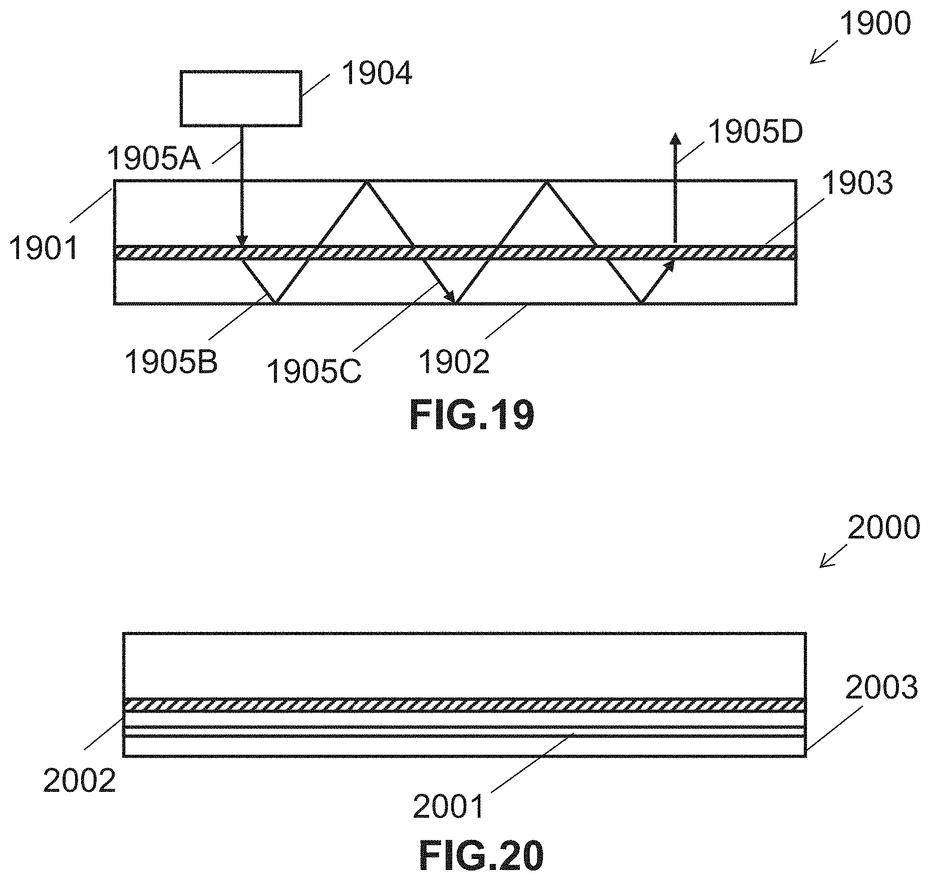
D00015

D00016

D00017
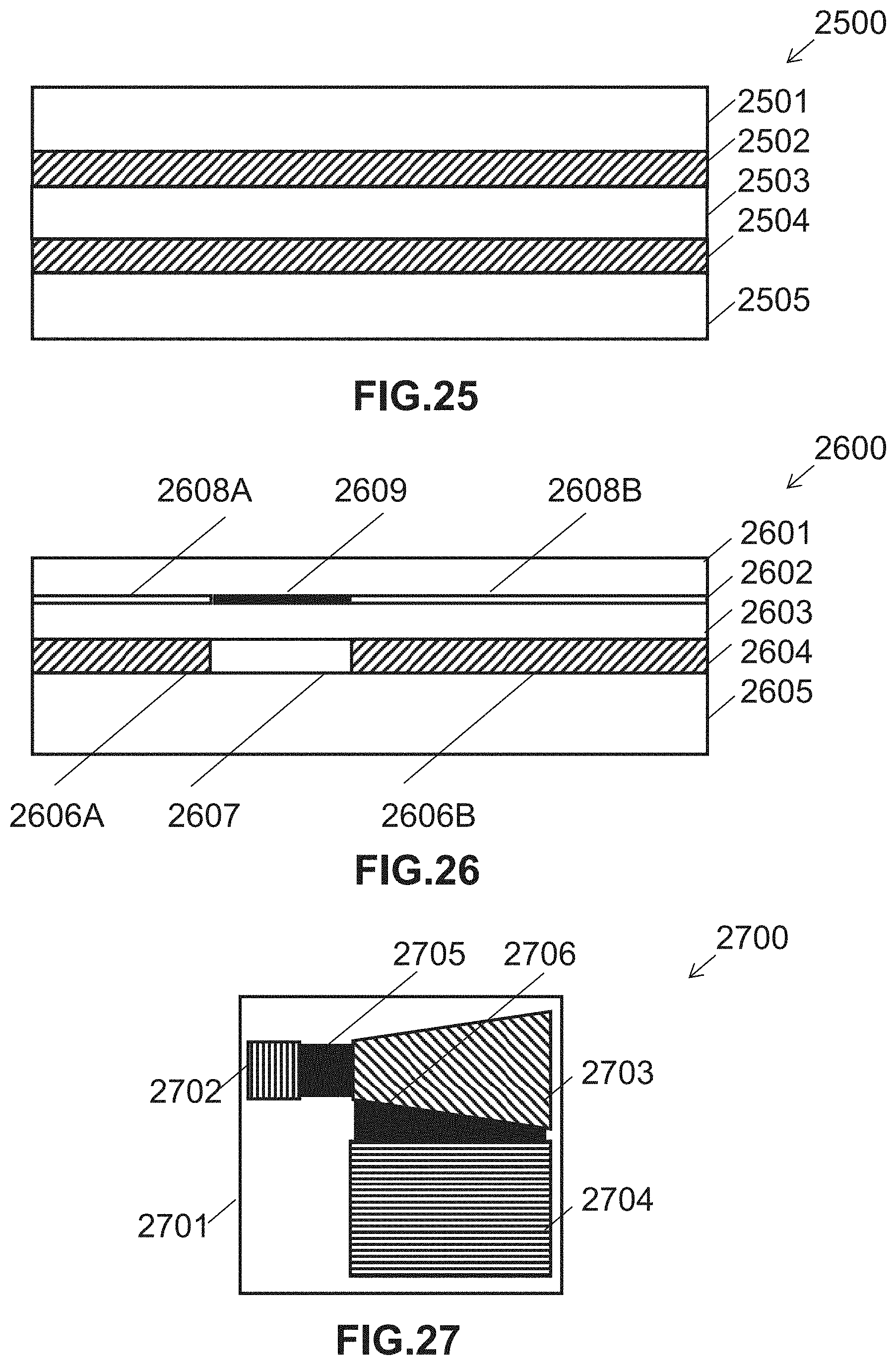
D00018
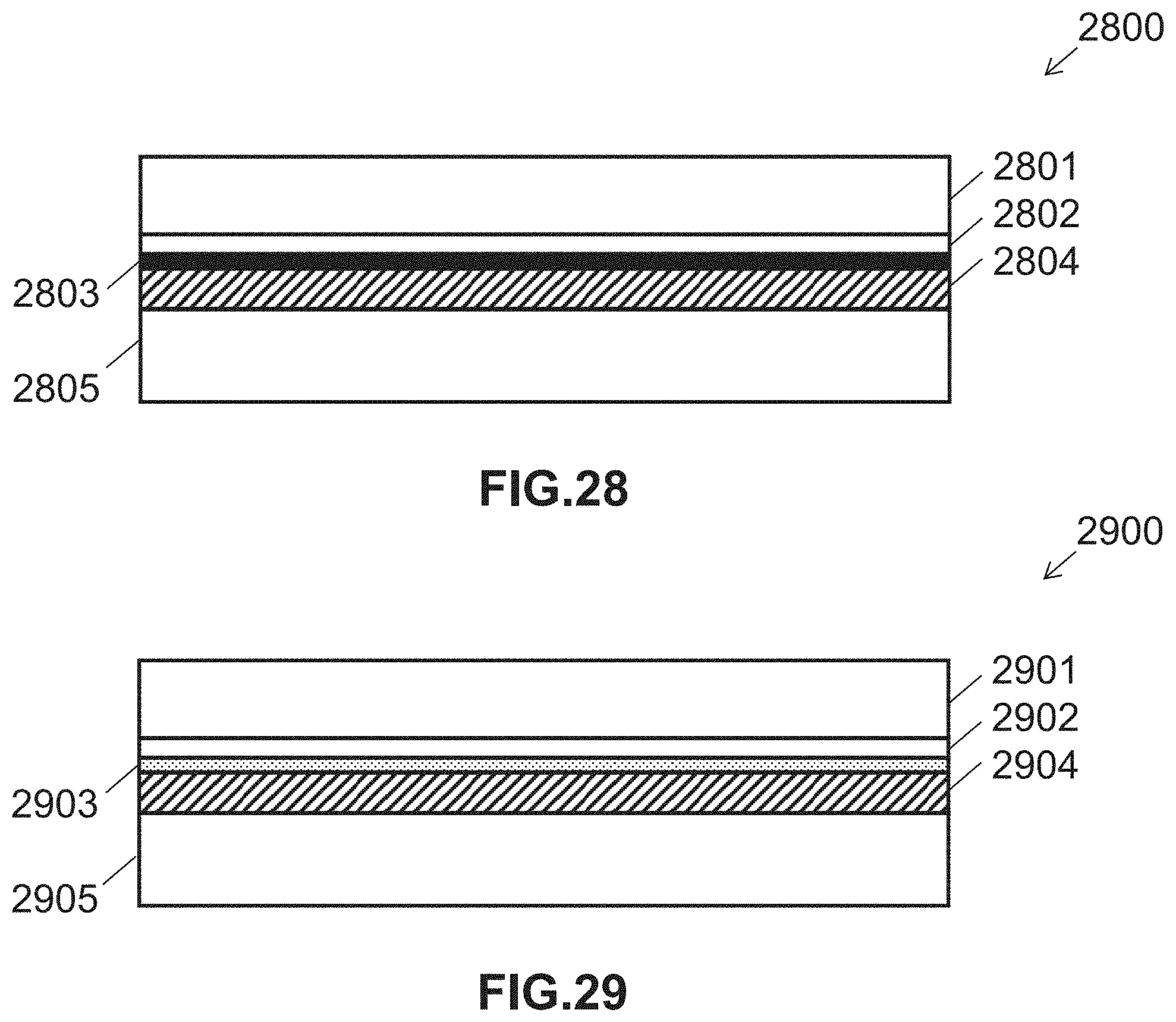
D00019
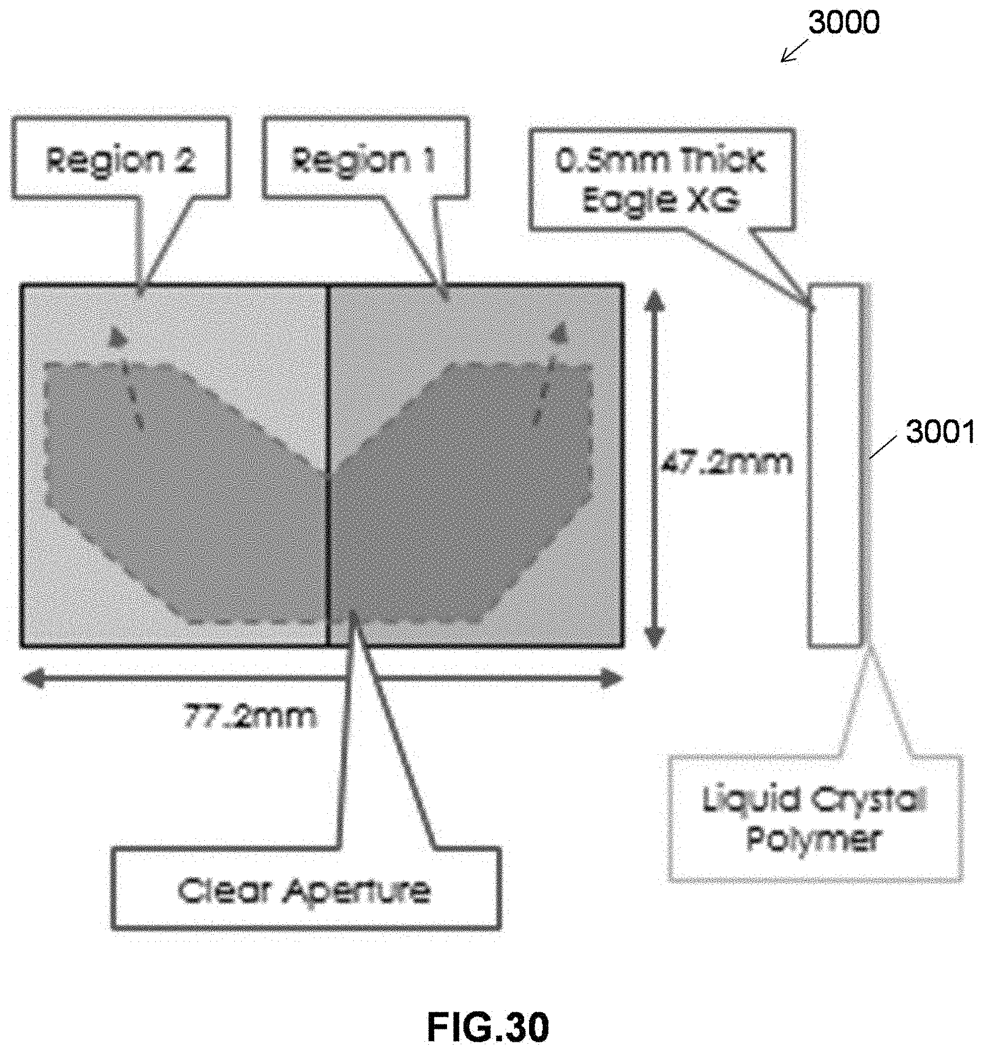
D00020
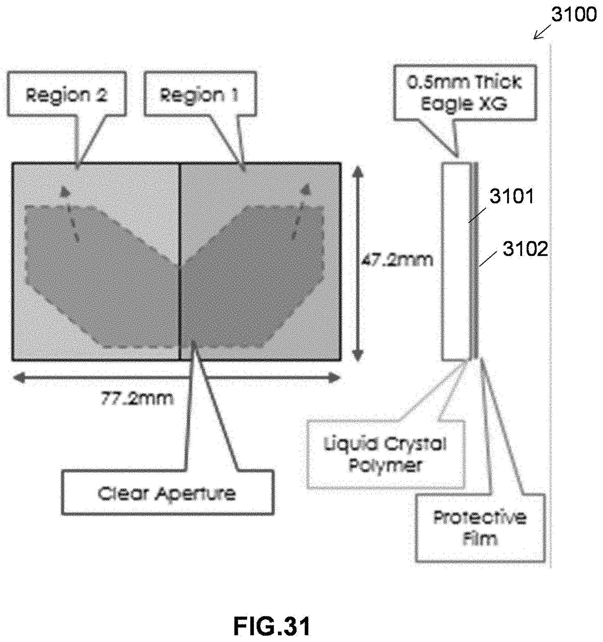
D00021

D00022
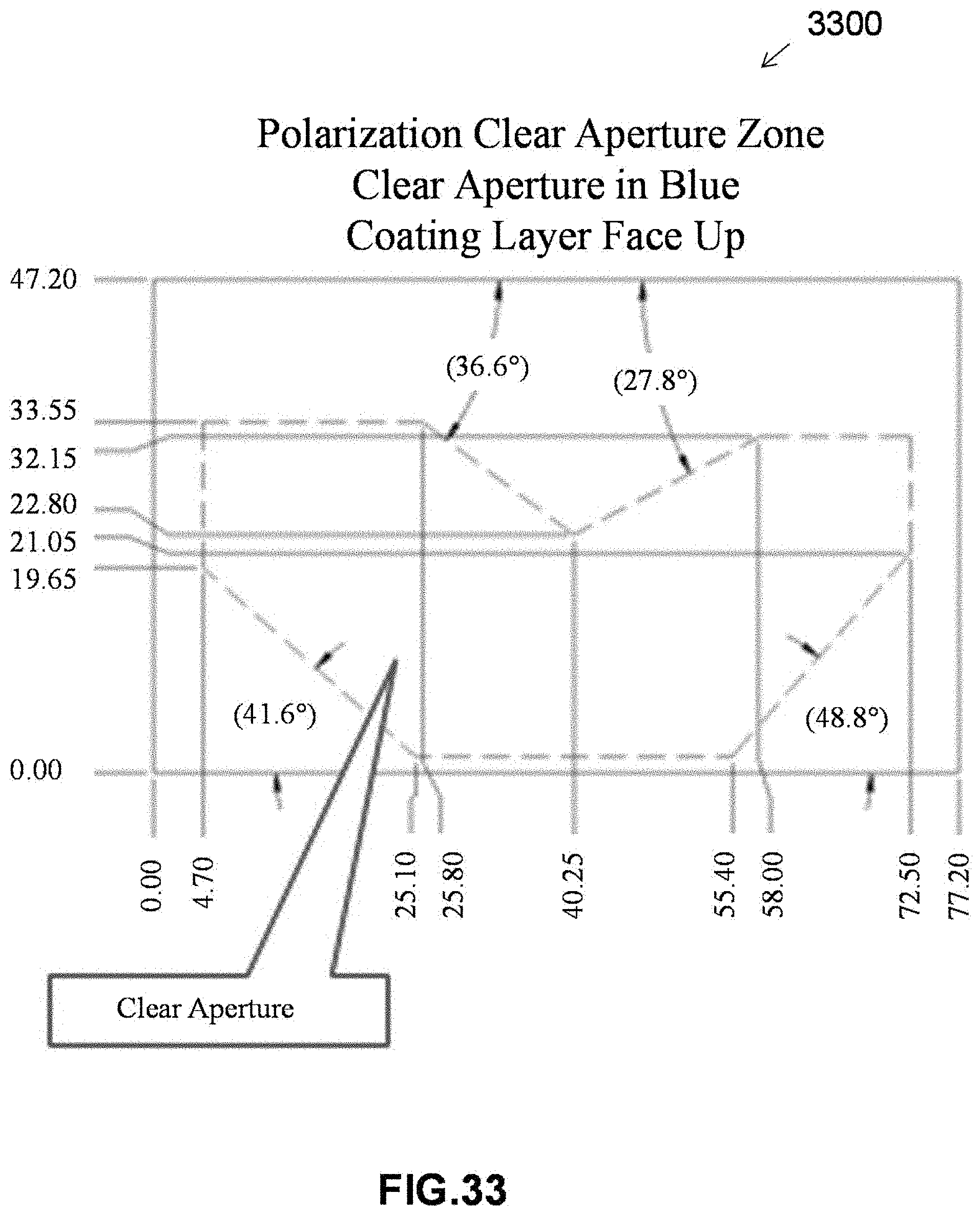
D00023

XML
uspto.report is an independent third-party trademark research tool that is not affiliated, endorsed, or sponsored by the United States Patent and Trademark Office (USPTO) or any other governmental organization. The information provided by uspto.report is based on publicly available data at the time of writing and is intended for informational purposes only.
While we strive to provide accurate and up-to-date information, we do not guarantee the accuracy, completeness, reliability, or suitability of the information displayed on this site. The use of this site is at your own risk. Any reliance you place on such information is therefore strictly at your own risk.
All official trademark data, including owner information, should be verified by visiting the official USPTO website at www.uspto.gov. This site is not intended to replace professional legal advice and should not be used as a substitute for consulting with a legal professional who is knowledgeable about trademark law.