Method and apparatus for contact image sensing
Popovich , et al.
U.S. patent number 10,591,756 [Application Number 15/562,755] was granted by the patent office on 2020-03-17 for method and apparatus for contact image sensing. This patent grant is currently assigned to DigiLens Inc.. The grantee listed for this patent is DigiLens Inc.. Invention is credited to Alastair John Grant, Milan Momcilo Popovich, Jonathan David Waldern.


View All Diagrams
| United States Patent | 10,591,756 |
| Popovich , et al. | March 17, 2020 |
Method and apparatus for contact image sensing
Abstract
A contact image sensor having a waveguiding structure for propagating light in a first direction including, in series, a first clad medium, a first core, a switchable grating clad, a second core, and a second clad medium sandwiched by transparent substrates, patterned parallel electrode elements orthogonally traversing the waveguides, a light source, a platen and a detector. Switchable grating regions overlapped by a first voltage-addressed electrode element diffract TIR light from the first core towards the platen. Switchable grating region overlapped by a second voltage-addressed electrode element diffract TIR light reflected from the platen into a TIR path within the second core.
| Inventors: | Popovich; Milan Momcilo (Leicester, GB), Waldern; Jonathan David (Los Altos Hills, CA), Grant; Alastair John (San Jose, CA) | ||||||||||
|---|---|---|---|---|---|---|---|---|---|---|---|
| Applicant: |
|
||||||||||
| Assignee: | DigiLens Inc. (Sunnyvale,
CA) |
||||||||||
| Family ID: | 55967320 | ||||||||||
| Appl. No.: | 15/562,755 | ||||||||||
| Filed: | March 30, 2016 | ||||||||||
| PCT Filed: | March 30, 2016 | ||||||||||
| PCT No.: | PCT/GB2016/000065 | ||||||||||
| 371(c)(1),(2),(4) Date: | September 28, 2017 | ||||||||||
| PCT Pub. No.: | WO2016/156776 | ||||||||||
| PCT Pub. Date: | October 06, 2016 |
Prior Publication Data
| Document Identifier | Publication Date | |
|---|---|---|
| US 20180074352 A1 | Mar 15, 2018 | |
Related U.S. Patent Documents
| Application Number | Filing Date | Patent Number | Issue Date | ||
|---|---|---|---|---|---|
| 62178041 | Mar 31, 2015 | ||||
| Current U.S. Class: | 1/1 |
| Current CPC Class: | G02F 1/1326 (20130101); G02F 1/29 (20130101); G02B 26/0808 (20130101); G02B 5/1828 (20130101); G02B 27/4272 (20130101) |
| Current International Class: | G02F 1/13 (20060101); G02B 27/42 (20060101); G02B 5/18 (20060101); G02F 1/29 (20060101); G02B 26/08 (20060101) |
| Field of Search: | ;250/221,237R,237G |
References Cited [Referenced By]
U.S. Patent Documents
| 1043938 | November 1912 | Huttenlocher |
| 3482498 | December 1969 | Becker |
| 3741716 | June 1973 | Johne et al. |
| 3843231 | October 1974 | Borel et al. |
| 3965029 | June 1976 | Arora |
| 3975711 | August 1976 | McMahon |
| 4035068 | July 1977 | Rawson |
| 4066334 | January 1978 | Fray et al. |
| 4248093 | February 1981 | Andersson et al. |
| 4251137 | February 1981 | Knop et al. |
| 4322163 | March 1982 | Schiller |
| 4386361 | May 1983 | Simmonds |
| 4389612 | June 1983 | Simmonds et al. |
| 4403189 | September 1983 | Simmonds |
| 4418993 | December 1983 | Lipton |
| 4472037 | September 1984 | Lipton |
| 4523226 | June 1985 | Lipton et al. |
| 4544267 | October 1985 | Schiller |
| 4562463 | December 1985 | Lipton |
| 4566758 | January 1986 | Bos et al. |
| 4583117 | April 1986 | Lipton et al. |
| 4643515 | February 1987 | Upatnieks |
| 4688900 | August 1987 | Doane et al. |
| 4711512 | December 1987 | Upatnieks |
| 4728547 | March 1988 | Vaz et al. |
| 4729640 | March 1988 | Sakata et al. |
| 4765703 | August 1988 | Suzuki et al. |
| 4791788 | December 1988 | Sager et al. |
| 4792850 | December 1988 | Liptoh et al. |
| 4811414 | March 1989 | Fishbine et al. |
| 4848093 | July 1989 | Simmonds et al. |
| 4884876 | December 1989 | Lipton et al. |
| 4890902 | January 1990 | Doane et al. |
| 4933976 | June 1990 | Fishbine et al. |
| 4938568 | July 1990 | Margerum et al. |
| 4960311 | October 1990 | Moss et al. |
| 4964701 | October 1990 | Dorschner et al. |
| 4967268 | October 1990 | Lipton et al. |
| 4970129 | November 1990 | Ingwall et al. |
| 4971719 | November 1990 | Vaz et al. |
| 4994204 | February 1991 | West |
| 5004323 | April 1991 | West |
| 5009483 | April 1991 | Rockwell et al. |
| 5033814 | July 1991 | Brown et al. |
| 5053834 | October 1991 | Simmonds |
| 5063441 | November 1991 | Lipton et al. |
| 5096282 | March 1992 | Margerum et al. |
| 5099343 | March 1992 | Margerum et al. |
| 5110034 | May 1992 | Simmonds et al. |
| 5117302 | May 1992 | Lipton |
| 5119454 | June 1992 | McMahon et al. |
| 5139192 | August 1992 | Simmonds et al. |
| 5142357 | August 1992 | Lipton et al. |
| 5142644 | August 1992 | Vansteenkiste et al. |
| 5148302 | September 1992 | Nagano et al. |
| 5181133 | January 1993 | Lipton |
| 5193000 | March 1993 | Lipton et al. |
| 5198912 | March 1993 | Ingwall et al. |
| 5200861 | April 1993 | Moskovich et al. |
| 5218480 | June 1993 | Moskovich et al. |
| 5224198 | June 1993 | Jachimowicz et al. |
| 5239372 | August 1993 | Lipton |
| 5240636 | August 1993 | Doane et al. |
| 5241337 | August 1993 | Betensky et al. |
| 5242476 | September 1993 | Bartel et al. |
| 5251048 | October 1993 | Doane et al. |
| 5264950 | November 1993 | West et al. |
| 5268792 | December 1993 | Kreitzer et al. |
| 5284499 | February 1994 | Harvey et al. |
| 5295208 | March 1994 | Caulfield et al. |
| 5296967 | March 1994 | Moskovich et al. |
| 5299289 | March 1994 | Omae et al. |
| 5309283 | May 1994 | Kreitzer et al. |
| 5313330 | May 1994 | Betensky |
| 5315324 | May 1994 | Simmonds et al. |
| 5315419 | May 1994 | Saupe et al. |
| 5315440 | May 1994 | Betensky et al. |
| 5327269 | July 1994 | Tilton et al. |
| 5329363 | July 1994 | Moskovich et al. |
| 5343147 | August 1994 | Sager et al. |
| 5368770 | November 1994 | Saupe et al. |
| 5371626 | December 1994 | Betensky |
| 5416510 | May 1995 | Lipton et al. |
| 5418871 | May 1995 | Revelli et al. |
| 5428480 | June 1995 | Betensky et al. |
| 5437811 | August 1995 | Doane et al. |
| 5452385 | September 1995 | Izumi et al. |
| 5453863 | September 1995 | West et al. |
| 5455693 | October 1995 | Wreede et al. |
| 5455713 | October 1995 | Kreitzer et al. |
| 5463428 | October 1995 | Lipton et al. |
| 5465311 | November 1995 | Caulfield et al. |
| 5476611 | December 1995 | Nolan et al. |
| 5481321 | January 1996 | Lipton |
| 5485313 | January 1996 | Betensky |
| 5493430 | February 1996 | Lu et al. |
| 5493448 | February 1996 | Betensky et al. |
| 5499140 | March 1996 | Betensky |
| 5500769 | March 1996 | Betensky |
| 5515184 | May 1996 | Caulfield et al. |
| 5516455 | May 1996 | Rakas et al. |
| 5530566 | June 1996 | Kumar |
| 5532875 | July 1996 | Betemsky |
| RE35310 | August 1996 | Moskovich |
| 5543950 | August 1996 | Lavrentovich et al. |
| 5559637 | September 1996 | Moskovich et al. |
| 5572250 | November 1996 | Lipton et al. |
| 5576888 | November 1996 | Betensky |
| 5585035 | December 1996 | Vesley et al. |
| 5593615 | January 1997 | Nerad et al. |
| 5619586 | April 1997 | Sibbald et al. |
| 5621529 | April 1997 | Gordon et al. |
| 5621552 | April 1997 | Coates et al. |
| 5625495 | April 1997 | Moskovich et al. |
| 5668614 | September 1997 | Chien et al. |
| 5677797 | October 1997 | Betensky et al. |
| 5680231 | October 1997 | Grinberg et al. |
| 5682255 | October 1997 | Friesem et al. |
| 5686931 | November 1997 | Fuenfschilling et al. |
| 5686975 | November 1997 | Lipton |
| 5691795 | November 1997 | Doane et al. |
| 5695682 | December 1997 | Doane et al. |
| 5706136 | January 1998 | Okuyama et al. |
| 5710645 | January 1998 | Phillips et al. |
| 5724463 | March 1998 | Deacon et al. |
| 5745266 | April 1998 | Smith et al. |
| 5745301 | April 1998 | Betensky et al. |
| 5748272 | May 1998 | Tanaka et al. |
| 5748277 | May 1998 | Huang et al. |
| 5751452 | May 1998 | Tanaka et al. |
| 5757546 | May 1998 | Lipton et al. |
| 5790314 | August 1998 | Duck et al. |
| 5798641 | August 1998 | Spagna et al. |
| 5808804 | September 1998 | Moskovich |
| 5822089 | October 1998 | Phillips et al. |
| 5825448 | October 1998 | Bos et al. |
| 5831700 | November 1998 | Li et al. |
| 5835661 | November 1998 | Tai et al. |
| 5841587 | November 1998 | Moskovich et al. |
| 5856842 | January 1999 | Tedesco |
| 5867238 | February 1999 | Miller et al. |
| 5870228 | February 1999 | Kreitzer et al. |
| 5875012 | February 1999 | Crawford et al. |
| 5877826 | March 1999 | Yang et al. |
| 5892599 | April 1999 | Bahuguna |
| 5900987 | May 1999 | Kreitzer et al. |
| 5900989 | May 1999 | Kreitzer |
| 5929960 | July 1999 | West et al. |
| 5930433 | July 1999 | Williamson et al. |
| 5936776 | August 1999 | Kreitzer |
| 5937115 | August 1999 | Domash |
| 5942157 | August 1999 | Sutherland et al. |
| 5949508 | September 1999 | Kumar et al. |
| 5956113 | September 1999 | Crawford |
| 5963375 | October 1999 | Kreitzer |
| 5966223 | October 1999 | Friesem et al. |
| 5969874 | October 1999 | Moskovich |
| 5969876 | October 1999 | Kreitzer et al. |
| 5973727 | October 1999 | McGrew et al. |
| 5974162 | October 1999 | Metz et al. |
| 5986746 | November 1999 | Metz et al. |
| 5999089 | December 1999 | Carlson et al. |
| 5999282 | December 1999 | Suzuki et al. |
| 6014187 | January 2000 | Okuda et al. |
| 6023375 | February 2000 | Kreitzer |
| 6046585 | April 2000 | Simmonds |
| 6052540 | April 2000 | Koyama |
| 6061107 | May 2000 | Yang |
| 6061463 | May 2000 | Metz et al. |
| 6094311 | July 2000 | Moskovich |
| 6097551 | August 2000 | Kreitzer |
| 6104448 | August 2000 | Doane et al. |
| 6115152 | September 2000 | Popovich et al. |
| 6118908 | September 2000 | Bischel et al. |
| 6128058 | October 2000 | Walton et al. |
| 6133971 | October 2000 | Silverstein et al. |
| 6133975 | October 2000 | Li et al. |
| 6141074 | October 2000 | Bos et al. |
| 6141154 | October 2000 | Kreitzer et al. |
| 6151142 | November 2000 | Phillips et al. |
| 6154190 | November 2000 | Yang et al. |
| 6167169 | December 2000 | Brinkman et al. |
| 6169594 | January 2001 | Aye et al. |
| 6169613 | January 2001 | Amitai et al. |
| 6169636 | January 2001 | Kreitzer et al. |
| 6188462 | February 2001 | Lavrentovich et al. |
| 6191887 | February 2001 | Michaloski et al. |
| 6195209 | February 2001 | Kreitzer et al. |
| 6204835 | March 2001 | Yang et al. |
| 6211976 | April 2001 | Popovich et al. |
| 6268839 | July 2001 | Yang et al. |
| 6269203 | July 2001 | Davies et al. |
| 6275031 | August 2001 | Simmonds et al. |
| 6278429 | August 2001 | Ruth et al. |
| 6297860 | October 2001 | Moskovich et al. |
| 6301056 | October 2001 | Kreitzer et al. |
| 6301057 | October 2001 | Kreitzer et al. |
| 6317228 | November 2001 | Popovich et al. |
| 6320563 | November 2001 | Yang et al. |
| 6324014 | November 2001 | Moskovich et al. |
| 6330109 | December 2001 | Ishii et al. |
| 6366281 | April 2002 | Lipton et al. |
| 6377238 | April 2002 | McPheters |
| 6377321 | April 2002 | Khan et al. |
| 6388797 | May 2002 | Lipton et al. |
| 6411444 | June 2002 | Moskovich et al. |
| 6414760 | July 2002 | Lopez et al. |
| 6417971 | July 2002 | Moskovich et al. |
| 6437563 | August 2002 | Simmonds et al. |
| 6445512 | September 2002 | Moskovich et al. |
| 6476974 | November 2002 | Kreitzer et al. |
| 6483303 | November 2002 | Simmonds et al. |
| 6504629 | January 2003 | Popovich et al. |
| 6509937 | January 2003 | Moskovich et al. |
| 6518747 | February 2003 | Sager et al. |
| 6519088 | February 2003 | Lipton |
| 6522794 | February 2003 | Bischel et al. |
| 6529336 | March 2003 | Kreitzer et al. |
| 6534977 | March 2003 | Duncan et al. |
| 6559813 | May 2003 | DeLuca et al. |
| 6563648 | May 2003 | Gleckman et al. |
| 6563650 | May 2003 | Moskovich et al. |
| 6567573 | May 2003 | Domash et al. |
| 6577411 | June 2003 | David et al. |
| 6577429 | June 2003 | Kurtz et al. |
| 6580529 | June 2003 | Amitai et al. |
| 6583838 | June 2003 | Hoke et al. |
| 6594090 | July 2003 | Kruschwitz et al. |
| 6597176 | July 2003 | Simmonds et al. |
| 6597475 | July 2003 | Shirakura et al. |
| 6600590 | July 2003 | Roddy et al. |
| 6618104 | September 2003 | Date et al. |
| 6625381 | September 2003 | Roddy et al. |
| 6646772 | November 2003 | Popovich et al. |
| 6667134 | December 2003 | Sutherland et al. |
| 6677086 | January 2004 | Bunning et al. |
| 6692666 | February 2004 | Sutherland et al. |
| 6699407 | March 2004 | Bunning et al. |
| 6706086 | March 2004 | Emig et al. |
| 6706451 | March 2004 | Sutherland et al. |
| 6730442 | May 2004 | Sutherland et al. |
| 6731434 | May 2004 | Hua et al. |
| 6738105 | May 2004 | Hannah et al. |
| 6747781 | June 2004 | Trisnadi et al. |
| 6791629 | September 2004 | Moskovich et al. |
| 6791739 | September 2004 | Ramanujan et al. |
| 6804066 | October 2004 | Ha et al. |
| 6805490 | October 2004 | Levola |
| 6821457 | November 2004 | Sutherland et al. |
| 6822713 | November 2004 | Yaroshchuk et al. |
| 6825987 | November 2004 | Repetto et al. |
| 6829095 | December 2004 | Amitai |
| 6830789 | December 2004 | Doane et al. |
| 6833955 | December 2004 | Niv |
| 6847488 | January 2005 | Travis |
| 6850210 | February 2005 | Lipton et al. |
| 6853493 | February 2005 | Kreitzer et al. |
| 6867888 | March 2005 | Sutherland et al. |
| 6878494 | April 2005 | Bunning et al. |
| 6927570 | August 2005 | Simmonds et al. |
| 6927694 | August 2005 | Smith et al. |
| 6950173 | September 2005 | Sutherland et al. |
| 6952435 | October 2005 | Lai et al. |
| 6958868 | October 2005 | Pender |
| 6963454 | November 2005 | Martins et al. |
| 6975345 | December 2005 | Lipton et al. |
| 6980365 | December 2005 | Moskovich |
| 6985296 | January 2006 | Lipton et al. |
| 6999239 | February 2006 | Martins et al. |
| 7002618 | February 2006 | Lipton et al. |
| 7002753 | February 2006 | Moskovich et al. |
| 7009773 | March 2006 | Chaoulov et al. |
| 7018563 | March 2006 | Sutherland et al. |
| 7018686 | March 2006 | Bunning et al. |
| 7019793 | March 2006 | Moskovich et al. |
| 7021777 | April 2006 | Amitai |
| 7026892 | April 2006 | Kajiya |
| 7054045 | May 2006 | McPheters et al. |
| 7068405 | June 2006 | Sutherland et al. |
| 7072020 | July 2006 | Sutherland et al. |
| 7075273 | July 2006 | O'Gorman et al. |
| 7077984 | July 2006 | Natarajan et al. |
| 7081215 | July 2006 | Natarajan et al. |
| 7088457 | August 2006 | Zou et al. |
| 7088515 | August 2006 | Lipton |
| 7099080 | August 2006 | Lipton et al. |
| 7108383 | September 2006 | Mitchell et al. |
| 7119965 | October 2006 | Rolland et al. |
| 7123421 | October 2006 | Moskovich et al. |
| 7133084 | November 2006 | Moskovich et al. |
| 7139109 | November 2006 | Mukawa |
| RE39424 | December 2006 | Moskovich |
| 7145729 | December 2006 | Kreitzer et al. |
| 7149385 | December 2006 | Parikka et al. |
| 7167286 | January 2007 | Anderson et al. |
| 7175780 | February 2007 | Sutherland et al. |
| 7181108 | February 2007 | Levola |
| 7184002 | February 2007 | Lipton et al. |
| 7184615 | February 2007 | Levola |
| 7186567 | March 2007 | Sutherland et al. |
| 7198737 | April 2007 | Natarajan et al. |
| 7206107 | April 2007 | Levola |
| 7230770 | June 2007 | Kreitzer et al. |
| 7256915 | August 2007 | Sutherland et al. |
| 7265882 | September 2007 | Sutherland et al. |
| 7265903 | September 2007 | Sutherland et al. |
| RE39911 | November 2007 | Moskovich |
| 7301601 | November 2007 | Lin et al. |
| 7312906 | December 2007 | Sutherland et al. |
| 7333685 | February 2008 | Stone et al. |
| 7375886 | May 2008 | Lipton et al. |
| 7391573 | June 2008 | Amitai |
| 7413678 | August 2008 | Natarajan et al. |
| 7413679 | August 2008 | Sutherland et al. |
| 7416818 | August 2008 | Sutherland et al. |
| 7418170 | August 2008 | Mukawa et al. |
| 7420733 | September 2008 | Natarajan et al. |
| 7453612 | November 2008 | Mukawa |
| 7454103 | November 2008 | Parriaux |
| 7457040 | November 2008 | Amitai |
| 7477206 | January 2009 | Cowan et al. |
| 7499217 | March 2009 | Cakmakci et al. |
| 7511891 | March 2009 | Messerschmidt et al. |
| 7522344 | April 2009 | Curatu et al. |
| 7570322 | August 2009 | Sutherland et al. |
| 7570405 | August 2009 | Sutherland et al. |
| 7577326 | August 2009 | Amitai |
| 7583423 | September 2009 | Sutherland et al. |
| 7589901 | September 2009 | DeJong et al. |
| 7605882 | October 2009 | Sutherland et al. |
| 7619739 | November 2009 | Sutherland et al. |
| 7639208 | December 2009 | Ha et al. |
| 7643214 | January 2010 | Amitai |
| 7672055 | March 2010 | Amitai |
| 7672549 | March 2010 | Schutz et al. |
| 7710622 | May 2010 | Takabayashi et al. |
| 7724443 | May 2010 | Amitai |
| 7740387 | June 2010 | Schultz et al. |
| 7747113 | June 2010 | Mukawa et al. |
| 7751122 | July 2010 | Amitai |
| 7751662 | July 2010 | Kleemann et al. |
| 7764413 | July 2010 | Levola |
| 7777819 | August 2010 | Simmonds |
| 7843642 | November 2010 | Shaoulov et al. |
| 7866869 | January 2011 | Karakawa |
| 7872707 | January 2011 | Sutherland et al. |
| 7884593 | February 2011 | Simmonds et al. |
| 7884985 | February 2011 | Amitai et al. |
| 7907342 | March 2011 | Simmonds et al. |
| 7936519 | May 2011 | Mukawa et al. |
| 7944616 | May 2011 | Mukawa |
| 7949214 | May 2011 | DeJong et al. |
| 7969657 | June 2011 | Cakmakci et al. |
| 8000020 | August 2011 | Amitai et al. |
| 8014050 | September 2011 | McGrew |
| 8016475 | September 2011 | Travis |
| 8018579 | September 2011 | Krah |
| 8023783 | September 2011 | Mukawa et al. |
| 8073296 | December 2011 | Mukawa et al. |
| 8077274 | December 2011 | Sutherland et al. |
| 8093451 | January 2012 | Simmonds et al. |
| 8098439 | January 2012 | Amitai et al. |
| 8107023 | January 2012 | Simmonds et al. |
| 8107780 | January 2012 | Simmonds |
| 8132948 | March 2012 | Owen et al. |
| 8134434 | March 2012 | Diederichs et al. |
| 8142016 | March 2012 | Legerton et al. |
| 8155489 | April 2012 | Saarikko et al. |
| 8160411 | April 2012 | Levola et al. |
| 8167173 | May 2012 | Simmonds et al. |
| 8194325 | June 2012 | Saarikko et al. |
| 8213065 | July 2012 | Mukawa |
| 8213755 | July 2012 | Mukawa et al. |
| 8220966 | July 2012 | Mukawa |
| 8224133 | July 2012 | Popovich et al. |
| 8233204 | July 2012 | Robbins et al. |
| 8294749 | October 2012 | Cable |
| 8310327 | November 2012 | Willers et al. |
| 8314993 | November 2012 | Levola et al. |
| 8320032 | November 2012 | Levola |
| 8325166 | December 2012 | Akutsu et al. |
| 8329773 | December 2012 | Facke et al. |
| 8335040 | December 2012 | Mukawa et al. |
| 8351744 | January 2013 | Travis et al. |
| 8354640 | January 2013 | Hamre et al. |
| 8355610 | January 2013 | Simmonds |
| 8369019 | February 2013 | Baker et al. |
| 8376548 | February 2013 | Schultz |
| 8382293 | February 2013 | Phillips, III et al. |
| 8384504 | February 2013 | Diederichs et al. |
| 8396339 | March 2013 | Mukawa et al. |
| 8422840 | April 2013 | Large |
| 8432614 | April 2013 | Amitai |
| 8441731 | May 2013 | Sprague |
| 8466953 | June 2013 | Levola et al. |
| 8472120 | June 2013 | Border et al. |
| 8481130 | July 2013 | Doornkamp et al. |
| 8482858 | July 2013 | Sprague |
| 8488246 | July 2013 | Border et al. |
| 8491136 | July 2013 | Travis et al. |
| 8493662 | July 2013 | Noui |
| 8494229 | July 2013 | Jarvenpaa et al. |
| 8520309 | August 2013 | Sprague |
| 8547638 | October 2013 | Levola |
| 8548290 | October 2013 | Travers et al. |
| 8565560 | October 2013 | Popovich et al. |
| 8582206 | November 2013 | Travis |
| 8593734 | November 2013 | Laakkonen |
| 8611014 | December 2013 | Valera et al. |
| 8634120 | January 2014 | Popovich et al. |
| 8639072 | January 2014 | Popovich et al. |
| 8643948 | February 2014 | Amitai et al. |
| 8649099 | February 2014 | Schultz et al. |
| 8654420 | February 2014 | Simmonds |
| 8659826 | February 2014 | Brown et al. |
| D701206 | March 2014 | Luckey et al. |
| 8698705 | April 2014 | Burke et al. |
| 8731350 | May 2014 | Jacobs et al. |
| 8736963 | May 2014 | Robbins et al. |
| 8746008 | June 2014 | Simmonds et al. |
| 8786923 | July 2014 | Chuang et al. |
| 8810913 | August 2014 | Simmonds et al. |
| 8810914 | August 2014 | Amitai |
| 8817350 | August 2014 | Robbins et al. |
| 8824836 | September 2014 | Sugiyama et al. |
| 8830584 | September 2014 | Saarikko et al. |
| 8842368 | September 2014 | Simmonds et al. |
| 8859412 | October 2014 | Jain |
| 8872435 | October 2014 | Montgomery et al. |
| 8873149 | October 2014 | Bohn et al. |
| 8873150 | October 2014 | Amitai |
| 8885997 | November 2014 | Bohn et al. |
| 8903207 | December 2014 | Brown et al. |
| 8906088 | December 2014 | Flitsch et al. |
| 8913865 | December 2014 | Bennett |
| 8917453 | December 2014 | Bohn et al. |
| 8937771 | January 2015 | Robbins et al. |
| 8950867 | February 2015 | Macnamara |
| 8964298 | February 2015 | Haddick et al. |
| 8965152 | February 2015 | Simmonds |
| 8985803 | March 2015 | Bohn et al. |
| 8989535 | March 2015 | Robbins |
| 9019595 | April 2015 | Jain |
| 9025253 | May 2015 | Hadad et al. |
| 9035344 | May 2015 | Jain |
| 9075184 | July 2015 | Popovich et al. |
| 9081178 | July 2015 | Simmonds et al. |
| 9128226 | September 2015 | Fattal et al. |
| 9129295 | September 2015 | Border et al. |
| 9164290 | October 2015 | Robbins et al. |
| 9201270 | December 2015 | Fattal et al. |
| 9215293 | December 2015 | Miller |
| 9253359 | February 2016 | Takahashi |
| 9269854 | February 2016 | Jain |
| 9274338 | March 2016 | Bohn et al. |
| 9310566 | April 2016 | Valera et al. |
| 9329325 | May 2016 | Simmonds et al. |
| 9341846 | May 2016 | Popovich et al. |
| 9354366 | May 2016 | Jain |
| 9366862 | June 2016 | Osterhout et al. |
| 9372347 | June 2016 | Saarikko et al. |
| 9377623 | June 2016 | Robbins et al. |
| 9389415 | July 2016 | Fattal et al. |
| 9400395 | July 2016 | Travers et al. |
| 9423360 | August 2016 | Tervonen et al. |
| 9431794 | August 2016 | Jain |
| 9459451 | October 2016 | Saarikko et al. |
| 9465213 | October 2016 | Simmonds |
| 9494799 | November 2016 | Robbins et al. |
| 9516193 | December 2016 | Aramaki |
| 9541383 | January 2017 | Watson et al. |
| 9547174 | January 2017 | Gao et al. |
| 9551874 | January 2017 | Amitai et al. |
| 9551880 | January 2017 | Amitai et al. |
| 9612403 | April 2017 | Watson et al. |
| 9632226 | April 2017 | Waldern et al. |
| 9651368 | May 2017 | Watson et al. |
| 9664824 | May 2017 | Simmonds et al. |
| 9664910 | May 2017 | Mansharof et al. |
| 9727772 | August 2017 | Popovich et al. |
| 9746688 | August 2017 | Popovich et al. |
| 9823423 | November 2017 | Waldern et al. |
| 10089516 | October 2018 | Popovich et al. |
| 2001/0043163 | November 2001 | Waldern et al. |
| 2001/0050756 | December 2001 | Lipton et al. |
| 2002/0003509 | January 2002 | Lipton et al. |
| 2002/0009299 | January 2002 | Lipton |
| 2002/0011969 | January 2002 | Lipton et al. |
| 2002/0036825 | March 2002 | Lipton et al. |
| 2002/0047837 | April 2002 | Suyama et al. |
| 2002/0110077 | August 2002 | Drobot et al. |
| 2002/0126332 | September 2002 | Popovich |
| 2002/0196332 | December 2002 | Lipton et al. |
| 2003/0007070 | January 2003 | Lipton et al. |
| 2003/0038912 | February 2003 | Broer et al. |
| 2003/0063884 | April 2003 | Smith et al. |
| 2003/0067685 | April 2003 | Niv |
| 2003/0086670 | May 2003 | Moridaira et al. |
| 2003/0107809 | June 2003 | Chen et al. |
| 2003/0197157 | October 2003 | Sutherland et al. |
| 2003/0202247 | October 2003 | Niv et al. |
| 2004/0004767 | January 2004 | Song |
| 2004/0089842 | May 2004 | Sutehrland et al. |
| 2004/0109234 | June 2004 | Levola |
| 2004/0112862 | June 2004 | Willson et al. |
| 2004/0141217 | July 2004 | Endo et al. |
| 2004/0175627 | September 2004 | Sutherland et al. |
| 2004/0179764 | September 2004 | Melikechi et al. |
| 2004/0263969 | December 2004 | Lipton et al. |
| 2004/0263971 | December 2004 | Lipton et al. |
| 2005/0018304 | January 2005 | Lipton et al. |
| 2005/0079663 | April 2005 | Masutani et al. |
| 2005/0105909 | May 2005 | Stone |
| 2005/0122395 | June 2005 | Lipton et al. |
| 2005/0134404 | June 2005 | Kajiya et al. |
| 2005/0141066 | June 2005 | Ouchi |
| 2005/0180687 | August 2005 | Amitai |
| 2005/0195276 | September 2005 | Lipton et al. |
| 2005/0232530 | October 2005 | Kekas et al. |
| 2005/0265585 | December 2005 | Rowe |
| 2005/0271258 | December 2005 | Rowe |
| 2005/0286133 | December 2005 | Lipton |
| 2006/0012878 | January 2006 | Lipton et al. |
| 2006/0043938 | March 2006 | O'Gorman et al. |
| 2006/0119837 | June 2006 | Raguin et al. |
| 2006/0132914 | June 2006 | Weiss et al. |
| 2006/0146422 | July 2006 | Koike |
| 2006/0171647 | August 2006 | Ye et al. |
| 2006/0191293 | August 2006 | Kuczma |
| 2006/0215244 | September 2006 | Yosha et al. |
| 2006/0228073 | October 2006 | Mukawa et al. |
| 2006/0268104 | November 2006 | Cowan et al. |
| 2006/0268412 | November 2006 | Downing et al. |
| 2006/0284974 | December 2006 | Lipton et al. |
| 2006/0285205 | December 2006 | Lipton et al. |
| 2006/0291052 | December 2006 | Lipton et al. |
| 2007/0012777 | January 2007 | Tsikos et al. |
| 2007/0019152 | January 2007 | Caputo et al. |
| 2007/0041684 | February 2007 | Popovich et al. |
| 2007/0070476 | March 2007 | Yamada et al. |
| 2007/0097502 | May 2007 | Lipton et al. |
| 2007/0109401 | May 2007 | Lipton et al. |
| 2007/0133089 | June 2007 | Lipton et al. |
| 2007/0154153 | July 2007 | Fomitchov et al. |
| 2007/0160325 | July 2007 | Son et al. |
| 2007/0177007 | August 2007 | Lipton et al. |
| 2007/0183650 | August 2007 | Lipton et al. |
| 2007/0188602 | August 2007 | Cowan et al. |
| 2007/0206155 | September 2007 | Lipton |
| 2007/0236560 | October 2007 | Lipton et al. |
| 2007/0237456 | October 2007 | Blauvelt et al. |
| 2007/0247687 | October 2007 | Handschy et al. |
| 2007/0258138 | November 2007 | Cowan et al. |
| 2007/0263169 | November 2007 | Lipton |
| 2008/0018851 | January 2008 | Lipton et al. |
| 2008/0024598 | January 2008 | Perlin et al. |
| 2008/0043334 | February 2008 | Itzkovitch et al. |
| 2008/0049100 | February 2008 | Lipton et al. |
| 2008/0062259 | March 2008 | Lipton et al. |
| 2008/0106775 | May 2008 | Amitai et al. |
| 2008/0106779 | May 2008 | Peterson et al. |
| 2008/0117289 | May 2008 | Schowengerdt et al. |
| 2008/0138013 | June 2008 | Parriaux |
| 2008/0143964 | June 2008 | Cowan et al. |
| 2008/0143965 | June 2008 | Cowan et al. |
| 2008/0149517 | June 2008 | Lipton et al. |
| 2008/0151370 | June 2008 | Cook et al. |
| 2008/0186573 | August 2008 | Lipton |
| 2008/0186574 | August 2008 | Robinson et al. |
| 2008/0198471 | August 2008 | Amitai |
| 2008/0226281 | September 2008 | Lipton |
| 2008/0239067 | October 2008 | Lipton |
| 2008/0239068 | October 2008 | Lipton |
| 2008/0273081 | November 2008 | Lipton |
| 2008/0285137 | November 2008 | Simmonds et al. |
| 2008/0297731 | December 2008 | Powell et al. |
| 2008/0298649 | December 2008 | Ennis et al. |
| 2008/0303895 | December 2008 | Akka et al. |
| 2008/0303896 | December 2008 | Lipton et al. |
| 2008/0304111 | December 2008 | Queenan et al. |
| 2008/0316303 | December 2008 | Chiu et al. |
| 2008/0316375 | December 2008 | Lipton et al. |
| 2009/0052047 | February 2009 | Amitai |
| 2009/0074356 | March 2009 | Sanchez et al. |
| 2009/0128495 | May 2009 | Kong et al. |
| 2009/0128911 | May 2009 | Itzkovitch et al. |
| 2009/0141324 | June 2009 | Mukawa |
| 2009/0190222 | July 2009 | Simmonds et al. |
| 2009/0242021 | October 2009 | Petkie et al. |
| 2009/0296218 | December 2009 | Ryytty |
| 2009/0303599 | December 2009 | Levola |
| 2010/0014312 | January 2010 | Travis et al. |
| 2010/0039796 | February 2010 | Mukawa |
| 2010/0053565 | March 2010 | Mizushima et al. |
| 2010/0079865 | April 2010 | Saarikko et al. |
| 2010/0086256 | April 2010 | Ben Bakir et al. |
| 2010/0097674 | April 2010 | Kasazumi et al. |
| 2010/0097820 | April 2010 | Owen et al. |
| 2010/0103078 | April 2010 | Mukawa et al. |
| 2010/0134534 | June 2010 | Seesselberg et al. |
| 2010/0149073 | June 2010 | Chaum et al. |
| 2010/0220293 | September 2010 | Mizushima et al. |
| 2010/0231532 | September 2010 | Nho et al. |
| 2010/0246003 | September 2010 | Simmonds et al. |
| 2010/0246004 | September 2010 | Simmonds |
| 2010/0284085 | November 2010 | Laakkonen |
| 2010/0284090 | November 2010 | Simmonds et al. |
| 2010/0284180 | November 2010 | Popovich et al. |
| 2010/0321781 | December 2010 | Levola et al. |
| 2011/0019874 | January 2011 | Jarvenpaa et al. |
| 2011/0026128 | February 2011 | Baker et al. |
| 2011/0032602 | February 2011 | Rothenberg et al. |
| 2011/0032618 | February 2011 | Handerek et al. |
| 2011/0032706 | February 2011 | Mukawa |
| 2011/0063604 | March 2011 | Hamre et al. |
| 2011/0102711 | May 2011 | Sutherland et al. |
| 2011/0109880 | May 2011 | Nummela |
| 2011/0187293 | August 2011 | Travis et al. |
| 2011/0235179 | September 2011 | Simmonds |
| 2011/0236803 | September 2011 | Weiser et al. |
| 2011/0242661 | October 2011 | Simmonds |
| 2011/0242670 | October 2011 | Simmonds |
| 2011/0249309 | October 2011 | McPheters et al. |
| 2011/0274435 | November 2011 | Fini et al. |
| 2012/0033306 | February 2012 | Valera et al. |
| 2012/0044572 | February 2012 | Simmonds et al. |
| 2012/0044573 | February 2012 | Simmonds et al. |
| 2012/0062850 | March 2012 | Travis |
| 2012/0062998 | March 2012 | Schultz et al. |
| 2012/0075168 | March 2012 | Osterhout et al. |
| 2012/0081789 | April 2012 | Mukawa et al. |
| 2012/0092632 | April 2012 | McLeod et al. |
| 2012/0120493 | May 2012 | Simmonds et al. |
| 2012/0162549 | June 2012 | Gao et al. |
| 2012/0183888 | July 2012 | Oliveira et al. |
| 2012/0194420 | August 2012 | Osterhout et al. |
| 2012/0200532 | August 2012 | Powell et al. |
| 2012/0206811 | August 2012 | Mukawa et al. |
| 2012/0206937 | August 2012 | Travis et al. |
| 2012/0207432 | August 2012 | Travis et al. |
| 2012/0207434 | August 2012 | Large et al. |
| 2012/0214089 | August 2012 | Honel et al. |
| 2012/0214090 | August 2012 | Weiser et al. |
| 2012/0235886 | September 2012 | Border et al. |
| 2012/0290973 | November 2012 | Robertson et al. |
| 2012/0300311 | November 2012 | Simmonds et al. |
| 2013/0016324 | January 2013 | Travis |
| 2013/0021392 | January 2013 | Travis |
| 2013/0021586 | January 2013 | Lippey |
| 2013/0033485 | February 2013 | Kollin et al. |
| 2013/0039619 | February 2013 | Laughlin et al. |
| 2013/0044376 | February 2013 | Valera et al. |
| 2013/0059233 | March 2013 | Askham |
| 2013/0069850 | March 2013 | Mukawa et al. |
| 2013/0077049 | March 2013 | Bohn |
| 2013/0117377 | May 2013 | Miller |
| 2013/0125027 | May 2013 | Abovitz et al. |
| 2013/0128230 | May 2013 | Macnamara |
| 2013/0143336 | June 2013 | Jain |
| 2013/0163089 | June 2013 | Bohn et al. |
| 2013/0176704 | July 2013 | Lanman et al. |
| 2013/0207887 | August 2013 | Raffle et al. |
| 2013/0224634 | August 2013 | Berneth et al. |
| 2013/0229717 | September 2013 | Amitai |
| 2013/0250207 | September 2013 | Bohn |
| 2013/0250430 | September 2013 | Robbins et al. |
| 2013/0250431 | September 2013 | Robbins et al. |
| 2013/0267309 | October 2013 | Robbins et al. |
| 2013/0271731 | October 2013 | Popovich et al. |
| 2013/0277890 | October 2013 | Bowman et al. |
| 2013/0322810 | December 2013 | Robbins |
| 2013/0342525 | December 2013 | Benko et al. |
| 2014/0003762 | January 2014 | Macnamara |
| 2014/0024159 | January 2014 | Jain |
| 2014/0055845 | February 2014 | Jain |
| 2014/0063055 | March 2014 | Osterhout et al. |
| 2014/0064655 | March 2014 | Bohn et al. |
| 2014/0071538 | March 2014 | Muller |
| 2014/0098010 | April 2014 | Travis |
| 2014/0104665 | April 2014 | Popovich et al. |
| 2014/0118647 | May 2014 | Momonoi et al. |
| 2014/0130132 | May 2014 | Cahill et al. |
| 2014/0140653 | May 2014 | Brown et al. |
| 2014/0140654 | May 2014 | Brown et al. |
| 2014/0146394 | May 2014 | Tout et al. |
| 2014/0160576 | June 2014 | Robbins et al. |
| 2014/0168735 | June 2014 | Yuan et al. |
| 2014/0168783 | June 2014 | Luebke et al. |
| 2014/0176528 | June 2014 | Robbins |
| 2014/0177023 | June 2014 | Gao et al. |
| 2014/0185286 | July 2014 | Popovich et al. |
| 2014/0198128 | July 2014 | Hong et al. |
| 2014/0204455 | July 2014 | Popovich et al. |
| 2014/0211322 | July 2014 | Bohn et al. |
| 2014/0218468 | August 2014 | Gao et al. |
| 2014/0218801 | August 2014 | Simmonds et al. |
| 2014/0232759 | August 2014 | Simmonds et al. |
| 2014/0240834 | August 2014 | Mason et al. |
| 2014/0240842 | August 2014 | Nguyen et al. |
| 2014/0267420 | September 2014 | Schowengerdt et al. |
| 2014/0300947 | October 2014 | Fattal et al. |
| 2014/0300960 | October 2014 | Santori et al. |
| 2014/0300966 | October 2014 | Travers et al. |
| 2014/0327970 | November 2014 | Bohn et al. |
| 2014/0330159 | November 2014 | Costa et al. |
| 2014/0367719 | December 2014 | Jain |
| 2014/0375542 | December 2014 | Robbins et al. |
| 2014/0375789 | December 2014 | Lou et al. |
| 2014/0375790 | December 2014 | Robbins et al. |
| 2015/0001677 | January 2015 | Venturato et al. |
| 2015/0003796 | January 2015 | Bennett |
| 2015/0010265 | January 2015 | Popovich et al. |
| 2015/0015946 | January 2015 | Muller |
| 2015/0016777 | January 2015 | Abovitz et al. |
| 2015/0035744 | February 2015 | Robbins et al. |
| 2015/0036068 | February 2015 | Fattal et al. |
| 2015/0058791 | February 2015 | Robertson et al. |
| 2015/0062675 | March 2015 | Ayres et al. |
| 2015/0062707 | March 2015 | Simmonds et al. |
| 2015/0086163 | March 2015 | Valera et al. |
| 2015/0125109 | May 2015 | Robbins et al. |
| 2015/0148728 | May 2015 | Sallum et al. |
| 2015/0185475 | July 2015 | Saarikko et al. |
| 2015/0235447 | August 2015 | Abovitz et al. |
| 2015/0235448 | August 2015 | Schowengerdt et al. |
| 2015/0260994 | September 2015 | Akutsu et al. |
| 2015/0268415 | September 2015 | Schowengerdt et al. |
| 2015/0277375 | October 2015 | Large et al. |
| 2015/0288129 | October 2015 | Jain |
| 2015/0346490 | December 2015 | Klug et al. |
| 2015/0346495 | December 2015 | Cheng et al. |
| 2015/0355394 | December 2015 | Leighton et al. |
| 2016/0003847 | January 2016 | Ryan et al. |
| 2016/0004090 | January 2016 | Popovich et al. |
| 2016/0026253 | January 2016 | Bradski et al. |
| 2016/0033705 | February 2016 | Fattal |
| 2016/0033706 | February 2016 | Fattal et al. |
| 2016/0038992 | February 2016 | Arthur et al. |
| 2016/0041387 | February 2016 | Valera et al. |
| 2016/0077338 | March 2016 | Nguyen et al. |
| 2016/0085300 | March 2016 | Robbins et al. |
| 2016/0116739 | April 2016 | Schowengerdt et al. |
| 2016/0124223 | May 2016 | Shinbo et al. |
| 2016/0132025 | May 2016 | Taff et al. |
| 2016/0195664 | July 2016 | Fattal et al. |
| 2016/0209648 | July 2016 | Haddick et al. |
| 2016/0231568 | August 2016 | Saarikko et al. |
| 2016/0238772 | August 2016 | Waldern et al. |
| 2016/0266398 | September 2016 | Poon et al. |
| 2016/0274362 | September 2016 | Tinch et al. |
| 2016/0283773 | September 2016 | Popovich et al. |
| 2016/0299344 | October 2016 | Dobschal et al. |
| 2016/0320536 | November 2016 | Ferns et al. |
| 2016/0327705 | November 2016 | Ferns et al. |
| 2016/0341964 | November 2016 | Amitai et al. |
| 2017/0003505 | January 2017 | Vallius et al. |
| 2017/0010488 | January 2017 | Schowengerdt et al. |
| 2017/0030550 | February 2017 | Popovich et al. |
| 2017/0031171 | February 2017 | Vallius et al. |
| 2017/0032166 | February 2017 | Raguin |
| 2017/0034435 | February 2017 | Vallius et al. |
| 2017/0038579 | February 2017 | Schuelke et al. |
| 2017/0052376 | February 2017 | Amitai et al. |
| 2017/0059759 | March 2017 | Ayres et al. |
| 2017/0102543 | April 2017 | Vallius et al. |
| 2017/0115487 | April 2017 | Travis et al. |
| 2017/0123208 | May 2017 | Vallius et al. |
| 2017/0131460 | May 2017 | Lin et al. |
| 2017/0131546 | May 2017 | Woltman et al. |
| 2017/0131551 | May 2017 | Woltman et al. |
| 2017/0180404 | June 2017 | Bersch et al. |
| 2017/0180408 | June 2017 | Yu et al. |
| 2017/0199333 | July 2017 | Waldern et al. |
| 2017/0219841 | August 2017 | Popovich et al. |
| 2017/0299860 | October 2017 | Juhola et al. |
| 2017/0357841 | December 2017 | Popovich et al. |
| 2018/0120669 | May 2018 | Popovich et al. |
| PI0720469 | Jan 2014 | BR | |||
| 2889727 | Jun 2014 | CA | |||
| 101103297 | Jan 2008 | CN | |||
| 100492099 | May 2009 | CN | |||
| 104204901 | Dec 2014 | CN | |||
| 104956252 | Sep 2015 | CN | |||
| 105074537 | Nov 2015 | CN | |||
| 105074539 | Nov 2015 | CN | |||
| 105190407 | Dec 2015 | CN | |||
| 105229514 | Jan 2016 | CN | |||
| 105393159 | Mar 2016 | CN | |||
| 105408801 | Mar 2016 | CN | |||
| 105408802 | Mar 2016 | CN | |||
| 105408803 | Mar 2016 | CN | |||
| 105531716 | Apr 2016 | CN | |||
| 105705981 | Jun 2016 | CN | |||
| 107466372 | Dec 2017 | CN | |||
| 19751190 | May 1999 | DE | |||
| 102012108424 | Mar 2014 | DE | |||
| 0795775 | Sep 1997 | EP | |||
| 1413972 | Apr 2004 | EP | |||
| 1526709 | Apr 2005 | EP | |||
| 1748305 | Jan 2007 | EP | |||
| 1413972 | Oct 2008 | EP | |||
| 2110701 | Oct 2009 | EP | |||
| 2244114 | Oct 2010 | EP | |||
| 2326983 | Jun 2011 | EP | |||
| 1828832 | May 2013 | EP | |||
| 2733517 | May 2014 | EP | |||
| 1573369 | Jul 2014 | EP | |||
| 2929378 | Oct 2015 | EP | |||
| 2748670 | Nov 2015 | EP | |||
| 2995986 | Mar 2016 | EP | |||
| 3256888 | Dec 2017 | EP | |||
| 2140935 | Dec 1984 | GB | |||
| 2508661 | Jun 2014 | GB | |||
| 2509536 | Jul 2014 | GB | |||
| 2512077 | Sep 2014 | GB | |||
| 2514658 | Dec 2014 | GB | |||
| 1204684 | Nov 2015 | HK | |||
| 1205563 | Dec 2015 | HK | |||
| 1205793 | Dec 2015 | HK | |||
| 1206101 | Dec 2015 | HK | |||
| 02186319 | Jul 1990 | JP | |||
| 03239384 | Oct 1991 | JP | |||
| 06294952 | Oct 1994 | JP | |||
| 07098439 | Apr 1995 | JP | |||
| 0990312 | Apr 1997 | JP | |||
| 11109320 | Apr 1999 | JP | |||
| 11142806 | May 1999 | JP | |||
| 2953444 | Sep 1999 | JP | |||
| 2000056259 | Feb 2000 | JP | |||
| 2000267042 | Sep 2000 | JP | |||
| 2001027739 | Jan 2001 | JP | |||
| 2001296503 | Oct 2001 | JP | |||
| 2002090858 | Mar 2002 | JP | |||
| 2002122906 | Apr 2002 | JP | |||
| 2002162598 | Jun 2002 | JP | |||
| 2002523802 | Jul 2002 | JP | |||
| 2003066428 | Mar 2003 | JP | |||
| 2003270419 | Sep 2003 | JP | |||
| 2008112187 | May 2008 | JP | |||
| 2009036955 | Feb 2009 | JP | |||
| 2009211091 | Sep 2009 | JP | |||
| 4367775 | Nov 2009 | JP | |||
| 2012137616 | Jul 2012 | JP | |||
| 5303928 | Oct 2013 | JP | |||
| 20100092059 | Aug 2010 | KR | |||
| 20140140063 | Dec 2014 | KR | |||
| 20140142337 | Dec 2014 | KR | |||
| 200535633 | Nov 2005 | TW | |||
| 200801583 | Jan 2008 | TW | |||
| 201314263 | Apr 2013 | TW | |||
| 201600943 | Jan 2016 | TW | |||
| 201604601 | Feb 2016 | TW | |||
| 1997001133 | Jan 1997 | WO | |||
| 1997027519 | Jul 1997 | WO | |||
| 1998004650 | Feb 1998 | WO | |||
| 1999009440 | Feb 1999 | WO | |||
| 2000016136 | Mar 2000 | WO | |||
| 2000023830 | Apr 2000 | WO | |||
| 2000023847 | Apr 2000 | WO | |||
| 2001050200 | Jul 2001 | WO | |||
| 2001090822 | Nov 2001 | WO | |||
| 2002082168 | Oct 2002 | WO | |||
| 2003081320 | Oct 2003 | WO | |||
| 2005001753 | Jan 2005 | WO | |||
| 2005006065 | Jan 2005 | WO | |||
| 2005006065 | Feb 2005 | WO | |||
| 2005073798 | Aug 2005 | WO | |||
| 2006002870 | Jan 2006 | WO | |||
| 2006064301 | Jun 2006 | WO | |||
| 2006064325 | Jun 2006 | WO | |||
| 2006064334 | Jun 2006 | WO | |||
| 2006102073 | Sep 2006 | WO | |||
| 2006132614 | Dec 2006 | WO | |||
| 2006102073 | Jan 2007 | WO | |||
| 2007015141 | Feb 2007 | WO | |||
| 2007029032 | Mar 2007 | WO | |||
| 2007085682 | Aug 2007 | WO | |||
| 2007130130 | Nov 2007 | WO | |||
| 2007141587 | Dec 2007 | WO | |||
| 2007141589 | Dec 2007 | WO | |||
| 2009013597 | Jan 2009 | WO | |||
| 2009077802 | Jun 2009 | WO | |||
| 2009077803 | Jun 2009 | WO | |||
| 2009101238 | Aug 2009 | WO | |||
| 2009155437 | Dec 2009 | WO | |||
| 2009155437 | Mar 2010 | WO | |||
| 2010023444 | Mar 2010 | WO | |||
| 2010057219 | May 2010 | WO | |||
| 2010067114 | Jun 2010 | WO | |||
| 2010104692 | Sep 2010 | WO | |||
| 2010122330 | Oct 2010 | WO | |||
| 2010125337 | Nov 2010 | WO | |||
| 2011032005 | Mar 2011 | WO | |||
| 2011042711 | Apr 2011 | WO | |||
| 2011051660 | May 2011 | WO | |||
| 2011055109 | May 2011 | WO | |||
| 2011073673 | Jun 2011 | WO | |||
| 2011107831 | Sep 2011 | WO | |||
| 2011110821 | Sep 2011 | WO | |||
| 2011131978 | Oct 2011 | WO | |||
| 2012052352 | Apr 2012 | WO | |||
| 2012062658 | May 2012 | WO | |||
| 2012158950 | Nov 2012 | WO | |||
| 2012172295 | Dec 2012 | WO | |||
| 2013027004 | Feb 2013 | WO | |||
| 2013027006 | Feb 2013 | WO | |||
| 2013034879 | Mar 2013 | WO | |||
| 2013049012 | Apr 2013 | WO | |||
| 2013102759 | Jul 2013 | WO | |||
| 2013167864 | Nov 2013 | WO | |||
| 2014064427 | May 2014 | WO | |||
| 2014080155 | May 2014 | WO | |||
| 2014085734 | Jun 2014 | WO | |||
| 2014090379 | Jun 2014 | WO | |||
| 2014091200 | Jun 2014 | WO | |||
| 2014093601 | Jun 2014 | WO | |||
| 2014100182 | Jun 2014 | WO | |||
| 2014113506 | Jul 2014 | WO | |||
| 2014116615 | Jul 2014 | WO | |||
| 2014130383 | Aug 2014 | WO | |||
| 2014144526 | Sep 2014 | WO | |||
| 2014159621 | Oct 2014 | WO | |||
| 2014164901 | Oct 2014 | WO | |||
| 2014176695 | Nov 2014 | WO | |||
| 2014179632 | Nov 2014 | WO | |||
| 2014188149 | Nov 2014 | WO | |||
| 2014209733 | Dec 2014 | WO | |||
| 2014209819 | Dec 2014 | WO | |||
| 2014209820 | Dec 2014 | WO | |||
| 2014209821 | Dec 2014 | WO | |||
| 2014210349 | Dec 2014 | WO | |||
| 2015006784 | Jan 2015 | WO | |||
| 2015015138 | Feb 2015 | WO | |||
| 2015017291 | Feb 2015 | WO | |||
| 2015069553 | May 2015 | WO | |||
| 2015081313 | Jun 2015 | WO | |||
| 2015117039 | Aug 2015 | WO | |||
| 2015145119 | Oct 2015 | WO | |||
| 2016010289 | Jan 2016 | WO | |||
| 2016020643 | Feb 2016 | WO | |||
| 2016025350 | Feb 2016 | WO | |||
| 2016046514 | Mar 2016 | WO | |||
| 2016103263 | Jun 2016 | WO | |||
| 2016111706 | Jul 2016 | WO | |||
| 2016111707 | Jul 2016 | WO | |||
| 2016111708 | Jul 2016 | WO | |||
| 2016111709 | Jul 2016 | WO | |||
| 2016113534 | Jul 2016 | WO | |||
| 2016118107 | Jul 2016 | WO | |||
| 2016122679 | Aug 2016 | WO | |||
| 2016156776 | Oct 2016 | WO | |||
| 2017060665 | Apr 2017 | WO | |||
| 2017162999 | Sep 2017 | WO | |||
| 2017180403 | Oct 2017 | WO | |||
Other References
|
US 9,488,474 B2, 11/2016, Abovitz et al. (withdrawn) cited by applicant . International Preliminary Report on Patentability for International Application No. PCT/GB2016/000065, issued Oct. 3, 2017, dated Oct. 12, 2017, 8 pgs. cited by applicant . International Preliminary Report on Patentability for International Application PCT/GB2009/051676, issued Jun. 14, 2011, dated Jun. 23, 2011, 6 pgs. cited by applicant . International Preliminary Report on Patentability for International Application PCT/GB2011/000349, issued Sep. 18, 2012, dated Sep. 27, 2012, 10 pgs. cited by applicant . International Preliminary Report on Patentability for International Application PCT/GB2012/000331, issued Oct. 8, 2013, dated Oct. 17, 2013, 8 pgs. cited by applicant . International Preliminary Report on Patentability for International Application PCT/GB2012/000677, issued Feb. 25, 2014, dated Mar. 6, 2014, 5 pgs. cited by applicant . International Preliminary Report on Patentability for International Application PCT/GB2013/000005, issued Jul. 8, 2014, dated Jul. 17, 2014, 12 pgs. cited by applicant . International Preliminary Report on Patentability for International Application PCT/GB2014/000295, issued Feb. 2, 2016, dated Feb. 11, 2016, 4 pgs. cited by applicant . International Preliminary Report on Patentability for International Application PCT/GB2015/000225, issued Feb. 14, 2017, dated Feb. 23, 2017, 8 pgs. cited by applicant . International Preliminary Report on Patentability for International application PCT/GB2015/000274, issued Mar. 28, 2017, dated Apr. 6, 2017, 8 pgs. cited by applicant . International Preliminary Report on Patentability for International Application PCT/GB2016/000014, issued Jul. 25, 2017, dated Aug. 3, 2017, 7 pgs. cited by applicant . International Preliminary Report on Patentability for International Application PCT/US2014/011736, issued Jul. 21, 2015, dated Jul. 30, 2015, 9 pgs. cited by applicant . International Preliminary Report on Patentability for International Application PCT/US2016/017091, issued Aug. 15, 2017, dated Aug. 24, 2017, 5 pgs. cited by applicant . International Search Report and Written Opinion for International Application PCT/GB2016/000065, completed Jul. 14, 2016, dated Jul. 27, 2016, 10 pgs. cited by applicant . International Search Report and Written Opinion for International Application PCT/US2014/011736, completed Apr. 18, 2014, dated May 8, 2014, 10 pgs. cited by applicant . International Search Report and Written Opinion for International Application PCT/GB2009/051675, completed May 10, 2010, dated May 18, 2010, 7 pgs. cited by applicant . International Search Report and Written Opinion for International Application PCT/US2016/017091, completed by the European Patent Office on Apr. 20, 2016, 7 pgs. cited by applicant . International Search Report for International Application No. PCT/GB2014/000295, completed Nov. 18, 2014, dated Jan. 5, 2015, 4 pgs. cited by applicant . International Search Report for International Application PCT/GB2017/000040, dated Jul. 18, 2017, completed Jul. 10, 2017, 3 pgs. cited by applicant . International Search Report for PCT/GB2011/000349, completed by the European Patent Office on Aug. 17, 2011, 4 pgs. cited by applicant . International Search Report for PCT/GB2012/000331, completed by the European Patent Office on Aug. 29, 2012, 4 pgs. cited by applicant . International Search Report for PCT/GB2012/000677, completed by the European Patent Office on Dec. 10, 2012, 4 pgs. cited by applicant . International Search Report for PCT/GB2013/000005, completed by the European Patent Office on Jul. 16, 2013, 3 pgs. cited by applicant . International Search Report for PCT/GB2015/000203, completed by the European Patent Office on Oct. 9, 2015, 4 pgs. cited by applicant . International Search Report for PCT/GB2015/000225, completed by the European Patent Office on Nov. 10, 2015, dated Dec. 2, 2016, 5 pgs. cited by applicant . International Search Report for PCT/GB2015/000274, completed by the European Patent Office on Jan. 7, 2016, 4 pgs. cited by applicant . International Search Report for PCT/GB2016/000014, completed by the European Patent Office on Jun. 27, 2016, 4 pgs. cited by applicant . Written Opinion for International Application No. PCT/GB2011/000349, completed Aug. 17, 2011, dated Aug. 25, 2011, 9 pgs. cited by applicant . Written Opinion for International Application No. PCT/GB2012/000331, completed Aug. 29, 2012, dated Sep. 6, 2012, 7 pgs. cited by applicant . Written Opinion for International Application No. PCT/GB2012/000677, completed Dec. 10, 2012, dated Dec. 17, 2012, 4 pgs. cited by applicant . Written Opinion for International Application No. PCT/GB2013/000005, search completed Jul. 16, 2013, dated Jul. 24, 2013, 11 pgs. cited by applicant . Written Opinion for International Application No. PCT/GB2014/000295, search completed Nov. 18, 2014, dated Jan. 5, 2015, 3 pgs. cited by applicant . Written Opinion for International Application No. PCT/GB2015/000225, search completed Nov. 10, 2015, dated Feb. 4, 2016, 7 pgs. cited by applicant . Written Opinion for International Application No. PCT/GB2015/000274, search completed Jan. 7, 2016, dated Jan. 19, 2016, 7 pgs. cited by applicant . Written Opinion for International Application No. PCT/GB2016/000014, search completed Jun. 27, 2016, dated Jul. 7, 2016, 6 pgs. cited by applicant . Written Opinion for International Application No. PCT/GB2017/000040, search completed Jul. 10, 2017, dated Jul. 18, 2017, 6 pgs. cited by applicant . "Agilent ADNS-2051 Optical Mouse Sensor: Data Sheet", Agilent Technologies, Jan. 9, 2002, 40 pgs. cited by applicant . "Application Note--MOXTEK ProFlux Polarizer use with LCOS displays", CRL Opto Limited, http://www.crlopto.com, 2003, 6 pgs. cited by applicant . "Application Note AN16: Optical Considerations for Bridgelux LED Arrays", BridgeLux, Jul. 31, 2010, 23 pgs. cited by applicant . "Application Note: Variable Attenuator for Lasers", Technology and Applications Center, Newport Corporation, www.newport.com, 2006, DS-08067, 6 pgs. cited by applicant . "Bae Systems to Unveil Q-Sight Family of Helmet-Mounted Display at AUSA Symposium", Released on Tuesday, Oct. 9, 2007, 1 pg. cited by applicant . "Beam Steering Using Liquid Crystals", Boulder Nonlinear Systems, Inc., info@bnonlinear.com, May 8, 2001, 4 pgs. cited by applicant . "BragGrate--Deflector: Transmitting Volume Bragg Grating for angular selection and magnification", 2015, www.OptiGrate.com. cited by applicant . "Cree XLamp XP-E LEDs", Cree, Inc., Retrieved from www.cree.com/Xlamp, CLD-DS18 Rev 17, 2013, 17 pgs. cited by applicant . "Desmodur N 3900", Bayer MaterialScience AG, Mar. 18, 2013, www.bayercoatings.com, 4 pgs. cited by applicant . "Digilens--Innovative Augmented Reality Display and Sensor Solutions for OEMs", Jun. 6, 2017, 31 pgs. cited by applicant . "Exotic Optical Components", Building Electro-Optical Systems, Making It All Work, Chapter 7, John Wiley & Sons, Inc., pp. 233-261. cited by applicant . "FHS Lenses Series", Fraen Corporation, www.fraen.com, Jun. 16, 2003, 10 pgs. cited by applicant . "FLP Lens Series for LUXEONTM Rebel and Rebel ES LEDs", Fraen Corporation, www.fraensrl.com, Aug. 7, 2015, 8 pgs. cited by applicant . "Head-up Displays, See-through display for military aviation", BAE Systems, 2016, 3 pgs. cited by applicant . "Holder for LUXEON Rebel--Part No. 180", Polymer Optics Ltd., 2008, 12 pgs. cited by applicant . "LED 7--Segment Displays", Lumex, uk.digikey.com, 2003, UK031, 36 pgs. cited by applicant . "LED325W UVTOP UV LED with Window", Thorlabs, Specifications and Documentation, 21978-S01 Rev. A, Apr. 8, 2011, 5 pgs. cited by applicant . "Liquid Crystal Phases", Phases of Liquid Crystals, http://plc.cwru.edu/tutorial/enhanced/files/lc/phase, Retrieved on Sep. 21, 2004, 6 pgs. cited by applicant . "LiteHUD Head-up display", BAE Systems, 2016, 2 pgs. cited by applicant . "LiteHUD Head-up display infographic", BAE Systems, 2017, 2 pgs. cited by applicant . "Luxeon C: Power Light Source", Philips Lumileds, www.philipslumileds.com, 2012, 18 pgs. cited by applicant . "Luxeon Rebel ES: Leading efficacy and light output, maximum design flexibility", LUXEON Rebel ES Datasheet DS61 20130221, www.philipslumileds.com, 2013, 33 pgs. cited by applicant . "Mobile Display Report", Insight Media, LLC, Apr. 2012, vol. 7, No. 4, 72 pgs. cited by applicant . "Molecular Imprints Imprio 55", Engineering at Illinois, Micro+ Nanotechnology Lab, Retrieved from https://mntl.illinois.edu/facilities/cleanrooms/equipment/Nano-Imprint.as- p, Dec. 28, 2015, 2 pgs. cited by applicant . "Optical measurements of retinal flow", Industrial Research Limited, Feb. 2012, 18 pgs. cited by applicant . "Osterhout Design Group Develops Next-Generation, Fully-integrated Smart Glasses Using Qualcomm Technologies", ODG, www.osterhoutgroup.com, Sep. 18, 2014, 2 pgs. cited by applicant . "Range Finding Using Pulse Lasers", OSRAM, Opto Semiconductors, Sep. 10, 2004, 7 pgs. cited by applicant . "Response time in Liquid-Crystal Variable Retarders", Meadowlark Optics, Inc., 2005, 4 pgs. cited by applicant . "Secondary Optics Design Considerations for SuperFlux LEDs", Lumileds, application brief AB20-5, Sep. 2002, 23 pgs. cited by applicant . "Solid-State Optical Mouse Sensor with Quadrature Outputs", IC Datasheet, UniqueICs, Jul. 15, 2004, 11 pgs. cited by applicant . "SVGA TransparentVLSITM Microdisplay Evaluation Kit", Radiant Images, Inc., Product Data Sheet, 2003, 3 pgs. cited by applicant . "Technical Data Sheet LPR1", Luminus Devices, Inc., Luminus Projection Chipset, Release 1, Preliminary, Revision B, Sep. 21, 2004, 9 pgs. cited by applicant . "The Next Generation of TV", SID Information Display, Nov./Dec. 2014, vol. 30, No. 6, 56 pgs. cited by applicant . "Thermal Management Considerations for SuperFlux LEDs", Lumileds, application brief AB20-4, Sep. 2002, 14 pgs. cited by applicant . "UVTOP240", Roithner LaserTechnik GmbH, v 2.0, Jun. 24, 2013, 6 pgs. cited by applicant . "UVTOP310", Roithner LaserTechnik GmbH, v 2.0, Jun. 24, 2013, 6 pgs. cited by applicant . "Velodyne's HDL-64E: A High Definition Lidar Sensor for 3-D Applications", High Definition Lidar, white paper, Oct. 2007, 7 pgs. cited by applicant . "VerLASE Gets Patent for Breakthrough Color Conversion Technology That Enables Full Color MicroLED Arrays for Near Eye Displays", Cision PRweb, Apr. 28, 2015, Retrieved from the Internet http://www.prweb.com/releases/2015/04/prweb12681038.htm, 3 pgs. cited by applicant . "X-Cubes--Revisited for LCOS", BASID, RAF Electronics Corp. Rawson Optics, Inc., Oct. 24, 2002, 16 pgs. cited by applicant . AACHEN, "Design of plastic optics for LED applications", Optics Colloquium 2009, Mar. 19, 2009, 30 pgs. cited by applicant . Abbate et al., "Characterization of LC-polymer composites for opto-electronic application", Proceedings of OPTOEL'03, Leganes-Madrid, Spain, Jul. 14-16, 2003, 4 pgs. cited by applicant . Al-Kalbani et al., "Ocular Microtremor laser speckle metrology", Proc. of SPIE, 2009, vol. 7176 717606-1, 12 pgs. cited by applicant . Almanza-Workman et al., "Planarization coating for polyimide substrates used in roll-to-roll fabrication of active matrix backplanes for flexible displays", HP Laboratories, HPL-2012-23, Feb. 6, 2012, 12 pgs. cited by applicant . Amundson et al., "Morphology and electro-optic properties of polymer-dispersed liquid-crystal films", Physical Review E, Feb. 1997, vol. 55, No. 2, pp. 1646-1654. cited by applicant . An et al., "Speckle suppression in laser display using several partially coherent beams", Optics Express, Jan. 5, 2009, vol. 17, No. 1, pp. 92-103. cited by applicant . Apter et al., "Electrooptical Wide-Angle Beam Deflector Based on Fringing-Field-Induced Refractive Inhomogeneity in a Liquid Crystal Layer", 23rd IEEE Convention of Electrical and Electronics Engineers in Israel, Sep. 6-7, 2004, pp. 240-243. cited by applicant . Arnold et al., "52.3: An Improved Polarizing Beamsplitter LCOS Projection Display Based on Wire-Grid Polarizers", Society for Information Display, Jun. 2001, pp. 1282-1285. cited by applicant . Ayras et al., "Exit pupil expander with a large field of view based on diffractive optics", Journal of the SID, May 18, 2009, 17/8, pp. 659-664. cited by applicant . Baets et al., "Resonant-Cavity Light-Emitting Diodes: a review", Proceedings of SPIE, 2003, vol. 4996, pp. 74-86. cited by applicant . Bayer et al., "Introduction to Helmet-Mounted Displays", 2016, pp. 47-108. cited by applicant . Beckel et al., "Electro-optic properties of thiol-ene polymer stabilized ferroelectric liquid crystals", Liquid Crystals, vol. 30, No. 11, Nov. 2003, pp. 1343-1350. cited by applicant . Bergkvist, "Biospeckle-based Study of the Line Profile of Light Scattered in Strawberries", Master Thesis, Lund Reports on Atomic Physics, LRAP-220, Lund 1997, pp. 1-62. cited by applicant . Bernards et al., "Nanoscale porosity in polymer films: fabrication and therapeutic applications", Soft Matter, Jan. 1, 2010, vol. 6, No. 8, pp. 1621-1631. cited by applicant . Bleha et al., "Binocular Holographic Waveguide Visor Display", SID Symposium Digest of Technical Papers, Holoeye Systems Inc., Jun. 2014, San Diego, CA, 4 pgs. cited by applicant . Bleha et al., W P. "D-ILA Technology for High Resolution Projection Displays", Sep. 10, 2003, Proceedings, vol. 5080, doi:10.1117/12.497532, 11 pgs. cited by applicant . Bone, "Design Obstacles for LCOS Displays in Projection Applications "Optics architectures for LCOS are still evolving"", Aurora Systems Inc., Bay Area SID Seminar, Mar. 27, 2001, 22 pgs. cited by applicant . Born et al., "Optics of Crystals", Principles of Optics 5th Edition 1975, pp. 705-707. cited by applicant . Bourzac, "Magic Leap Needs to Engineer a Miracle", Intelligent Machines, Jun. 11, 2015, 7 pgs. cited by applicant . Bowen et al., "Optimisation of interdigitated electrodes for piezoelectric actuators and active fibre composites", J Electroceram, Jul. 2006, vol. 16, pp. 263-269, DOI 10.1007/s10832-006-9862-8. cited by applicant . Bowley et al., "Variable-wavelength switchable Bragg gratings formed in polymer-dispersed liquid crystals", Applied Physics Letters, Jul. 2, 2001, vol. 79, No. 1, pp. 9-11. cited by applicant . Bronnikov et al., "Polymer-Dispersed Liquid Crystals: Progress in Preparation, Investigation and Application", Journal of Macromolecular Science Part B, published online Sep. 30, 2013, vol. 52, pp. 1718-1738. cited by applicant . Brown, "Waveguide Displays", Rockwell Collins, 2015, 11 pgs. cited by applicant . Bruzzone et al., "Compact, high-brightness LED illumination for projection systems", Journal of the SID 17/12, Dec. 2009, pp. 1043-1049. cited by applicant . Buckley, "Colour holographic laser projection technology for heads-up and instrument cluster displays", Conference: Proc. SID Conference 14th Annual Symposium on Vehicle Displays, Jan. 2007, 5 pgs. cited by applicant . Buckley, "Pixtronix DMS technology for head-up displays", Pixtronix, Inc., Jan. 2011, 4 pgs. cited by applicant . Buckley et al., "Full colour holographic laser projector HUD", Light Blue Optics Ltd., Aug. 10, 2015, 5 pgs. cited by applicant . Buckley et al., "Rear-view virtual image displays", in Proc. SID Conference 16th Annual Symposium on Vehicle Displays, Jan. 2009, 5 pgs. cited by applicant . Bunning et al., "Effect of gel-point versus conversion on the real-time dynamics of holographic polymer-dispersed liquid crystal (HPDLC) formation", Proceedings of SPIE--vol. 5213, Liquid Crystals VII, Iam-Choon Khoo, Editor, Dec. 2003, pp. 123-129. cited by applicant . Bunning et al., "Electro-optical photonic crystals formed in H-PDLCs by thiol-ene photopolymerization", American Physical Society, Annual APS, Mar. 3-7, 2003, abstract #R1.135. cited by applicant . Bunning et al., "Holographic Polymer-Dispersed Liquid Crystals (H-PDLCs)1", Annu. Rev. Mater. Sci., 2000, vol. 30, pp. 83-115. cited by applicant . Bunning et al., "Morphology of Anisotropic Polymer Dispersed Liquid Crystals and the Effect of Monomer Functionality", Polymer Science: Part B: Polymer Physics, Jul. 30, 1997, vol. 35, pp. 2825-2833. cited by applicant . Busbee et al., "SiO2 Nanoparticle Sequestration via Reactive Functionalization in Holographic Polymer-Dispersed Liquid Crystals", Advanced Materials, Sep. 2009, vol. 21, pp. 3659-3662. cited by applicant . Butler et al., "Diffractive Properties of Highly Birefringent Volume Gratings: Investigation", Journal of Optical Society of America, Feb. 2002, vol. 19, No. 2, pp. 183-189. cited by applicant . Cai et al., "Recent advances in antireflective surfaces based on nanostructure arrays", Mater. Horiz., 2015, vol. 2, pp. 37-53. cited by applicant . Cameron, "Optical Waveguide Technology & Its Application in Head Mounted Displays", Proc. of SPIE, May 22, 2012, vol. 8383, pp. 83830E-1-83830E-11. cited by applicant . Caputo et al., "POLICRYPS Composite Materials: Features and Applications", Advances in Composite Materials--Analysis of Natural and Man-Made Materials, www.intechopen.com, Sep. 2011, pp. 93-118. cited by applicant . Caputo et al., "POLICRYPS Switchable Holographic Grating: A Promising Grating Electro-Optical Pixel for High Resolution Display Application", Journal of Display Technology, Mar. 2006, vol. 2, No. 1, pp. 38-51. cited by applicant . Carclo Optics, "Guide to choosing secondary optics", Carclo Optics, Dec. 15, 2014, www.carclo-optics.com, 48 pgs. cited by applicant . Chen et al, "Polarization rotators fabricated by thermally-switched liquid crystal alignments based on rubbed poly(N-vinyl carbazole) films", Optics Express, Apr. 11, 2011, vol. 19, No. 8, pp. 7553-7558. cited by applicant . Cheng et al., "Design of an ultra-thin near-eye display with geometrical waveguide and freeform optics", Optics Express, Aug. 2014, 16 pgs. cited by applicant . Chi et al., "Ultralow-refractive-index optical thin films through nanoscale etching of ordered mesoporous silica films", Optic Letters, May 1, 2012, vol. 37, No. 9, pp. 1406-1408. cited by applicant . Chigrinov et al., "Photo-aligning by azo-dyes: Physics and applications", Liquid Crystals Today, Sep. 6, 2006, http://www.tandfonline.com/action/journalInformation?journalCode=tlcy20, 15 pgs. cited by applicant . Cho et al., "Electro-optic Properties of CO2 Fixed Polymer/Nematic LC Composite Films", Journal of Applied Polymer Science, Nov. 5, 2000, vol. 81, Issue 11, pp. 2744-2753. cited by applicant . Cho et al., "Fabrication of Reflective Holographic PDLC for Blue", Molecular Crystals and Liquid Crystals Science, 2001, vol. 368, pp. 3845-3853. cited by applicant . Cho et al., "Optimization of Holographic Polymer Dispersed Liquid Crystals for Ternary Monomers", Polymer International, Nov. 1999, vol. 48, pp. 1085-1090. cited by applicant . Colegrove et al., "P-59: Technology of Stacking HPDLC for Higher Reflectance", SID 00 DIGEST, May 2000, pp. 770-773. cited by applicant . Cruz-Arreola et al., "Diffraction of beams by infinite or finite amplitude-phase gratings", Investigacio' N Revista Mexicana de Fi'Sice, Feb. 2011, vol. 57, No. 1, pp. 6-16. cited by applicant . Dainty, "Some statistical properties of random speckle patterns in coherent and partially coherent illumination", Optica Acta, Mar. 12, 1970, vol. 17, No. 10, pp. 761-772. cited by applicant . Date, "Alignment Control in Holographic Polymer Dispersed Liquid Crystal", Journal of Photopolymer Science and Technology, Nov. 2, 2000, vol. 13, pp. 289-284. cited by applicant . Date et al., "52.3: Direct-viewing Display Using Alignment-controlled PDLC and Holographic PDLC", Society for Information Display Digest, May 2000, pp. 1184-1187, DOI: 10.1889/1.1832877. cited by applicant . Date et al., "Full-color reflective display device using holographically fabricated polymer-dispersed liquid crystal (HPDLC)", Journal of the SID, 1999, vol. 7, No. 1, pp. 17-22. cited by applicant . De Bitetto, "White light viewing of surface holograms by simple dispersion compensation", Applied Physics Letters, Dec. 15, 1966, vol. 9, No. 12, pp. 417-418. cited by applicant . Developer World, "Create customized augmented reality solutions", printed Oct. 19, 2017, LMX-001 holographic waveguide display, Sony Developer World, 3 pgs. cited by applicant . Dhar et al., "Recording media that exhibit high dynamic range for digital holographic data storage", Optics Letters, Apr. 1, 1999, vol. 24, No. 7, pp. 487-489. cited by applicant . Domash et al., "Applications of switchable Polaroid holograms", SPIE Proceedings, vol. 2152, Diffractive and Holographic Optics Technology, Jan. 23-29, 1994, Los Angeles, CA, pp. 127-138, ISBN: 0-8194-1447-6. cited by applicant . Drake et al., "Waveguide Hologram Fingerprint Entry Device", Optical Engineering, Sep. 1996, vol. 35, No. 9, pp. 2499-2505. cited by applicant . Drevensek-Olenik et al., "In-Plane Switching of Holographic Polymer-Dispersed Liquid Crystal Transmission Gratings", Mol. Cryst. Liq. Cryst., 2008, vol. 495, pp. 177/[529]-185/[537]. cited by applicant . Drevensek-Olenik et al., "Optical diffraction gratings from polymer-dispersed liquid crystals switched by interdigitated electrodes", Journal of Applied Physics, Dec. 1, 2004, vol. 96, No. 11, pp. 6207-6212. cited by applicant . Ducharme, "Microlens diffusers for efficient laser speckle generation", Optics Express, Oct. 29, 2007, vol. 15, No. 22, pp. 14573-14579. cited by applicant . Duong et al., "Centrifugal Deposition of Iron Oxide Magnetic Nanorods for Hyperthermia Application", Journal of Thermal Engineering, Yildiz Technical University Press, Istanbul, Turkey, Apr. 2015, vol. 1, No. 2, pp. 99-103. cited by applicant . Fattal et al., "A multi directional backlight for a wide-angle glasses-free three-dimensional display", Nature, Mar. 21, 2012, vol. 495, pp. 348-351. cited by applicant . Fontecchio et al., "Spatially Pixelated Reflective Arrays from Holographic Polymer Dispersed Liquid Crystals", SID 00 Digest, May 2000, pp. 774-776. cited by applicant . Forman et al., "Materials development for PhotoINhibited SuperResolution (PINSR) lithography", Proc. of SPIE, 2012, vol. 8249, 824904, doi: 10.1117/12.908512, pp. 824904-1-824904-9. cited by applicant . Forman et al., "Radical diffusion limits to photoinhibited superresolution lithography", Phys.Chem. Chem. Phys., May 31, 2013, vol. 15, pp. 14862-14867. cited by applicant . Friedrich-Schiller, "Spatial Noise and Speckle", Version 1.12.2011, Dec. 2011, Abbe School of Photonics, Jena, Germany, 27 pgs. cited by applicant . Fujii et al., "Nanoparticle-polymer-composite volume gratings incorporating chain-transfer agents for holography and slow-neutron optics", Optics Letters, Apr. 25, 2014, vol. 39, Issue 12, 5 pgs. cited by applicant . Funayama et al., "Proposal of a new type thin film light-waveguide display device using", The International Conference on Electrical Engineering, 2008, No. P-044, 5 pgs. cited by applicant . Gabor, "Laser Speckle and its Elimination", BM Research and Development, Eliminating Speckle Noise, Sep. 1970, vol. 14, No. 5, pp. 509-514. cited by applicant . Gardiner et al., "Bistable liquid-crystals reduce power consumption for high-efficiency smart glazing", SPIE, 2009, 10.1117/2.1200904.1596, 2 pgs. cited by applicant . Giancola, "Holographic Diffuser, Makes Light Work of Screen Tests", Photonics Spectra, 1996, vol. 30, No. 8, p. 121. cited by applicant . Goodman, "Some fundamental properties of speckle", J. Opt. Soc. Am., Nov. 1976, vol. 66, No. 11, pp. 1145-1150. cited by applicant . Goodman, "Statistical Properties of Laser Speckle Patterns", Applied Physics, 1975, vol. 9, Chapter 2, Laser Speckle and Related Phenomena, pp. 9-75. cited by applicant . Goodman et al., "Speckle Reduction by a Moving Diffuser in Laser Projection Displays", The Optical Society of America, 2000, 15 pgs. cited by applicant . Guldin et al., "Self-Cleaning Antireflective Optical Coatings", Nano Letters, Oct. 14, 2013, vol. 13, pp. 5329-5335. cited by applicant . Guo et al., "Review Article: A Review of the Optimisation of Photopolymer Materials for Holographic Data Storage", Physics Research International, vol. 2012, Article ID 803439, Academic Editor: Sergi Gallego, 16 pages, http://dx.doi.org/10.1155/2012/803439, May 4, 2012. cited by applicant . Ha et al., "Optical Security Film Based on Photo-alignment Technology", Department of Electronic & Computer Engineering, May 9, 2016, 1 pg. cited by applicant . Han et al., "Study of Holographic Waveguide Display System", Advanced Photonics for Communications, 2014, 4 pgs. cited by applicant . Harbers et al., "I-15.3: LED Backlighting for LCD-HDTV", Journal of the Society for Information Display, 2002, vol. 10, No. 4, pp. 347-350. cited by applicant . Harbers et al., "Performance of High Power LED Illuminators in Color Sequential Projection Displays", Lumileds Lighting, 2007, 4 pgs. cited by applicant . Harbers et al., "Performance of High Power LED Illuminators in Color Sequential Projection Displays", Lumileds, Aug. 7, 2001, 11 pgs. cited by applicant . Harbers et al., "Performance of High-Power LED illuminators in Projection Displays", Proc. Int. Disp. Workshops, Japan. vol. 10, pp. 1585-1588, 2003. cited by applicant . Harding et al., "Reactive Liquid Crystal Materials for Optically Anisotropic Patterned Retarders", Merck, Iicrivue, 2008, ME-GR-RH-08-010, 20 pgs. cited by applicant . Harding et al., "Reactive Liquid Crystal Materials for Optically Anisotropic Patterned Retarders", SPIE Lithography Asia--Taiwan, 2008, Proceedings vol. 7140, Lithography Asia 2008; 71402J, doi: 10.1117/12.805378. cited by applicant . Hariharan, "Optical Holography: Principles, techniques and applications", Cambridge University Press, 1996, pp. 231, 233. cited by applicant . Harris, "Photonic Devices", EE 216 Principals and Models of Semiconductor Devices, Autumn 2002, 20 pgs. cited by applicant . Harrold et al., "3D Display Systems Hardware Research at Sharp Laboratories of Europe: an update", Sharp Laboratories of Europe, Ltd., received May 21, 1999, 7 pgs. cited by applicant . Harthong et al., "Speckle phase averaging in high-resolution color holography", J. Opt. Soc. Am. A, Feb. 1997, vol. 14, No. 2, pp. 405-409. cited by applicant . Hasan et al., "Tunable-focus lens for adaptive eyeglasses", Optics Express, Jan. 23, 2017, vol. 25, No. 2, 1221, 13 pgs. cited by applicant . Hasman et al., "Diffractive Optics: Design, Realization, and Applications", Fiber and Integrated Optics, vol. 16, pp. 1-25, 1997. cited by applicant . Hata et al., "Holographic nanoparticle-polymer composites based on step-growth thiol-ene photopolymerization", Optical Materials Express, Jun. 1, 2011, vol. 1, No. 2, pp. 207-222. cited by applicant . He et al., "Dynamics of peristrophic multiplexing in holographic polymer-dispersed liquid crystal", Liquid Crystals, Mar. 26, 2014, vol. 41, No. 5, pp. 673-684. cited by applicant . He et al., "Holographic 3D display based on polymer-dispersed liquid-crystal thin films", Proceedings of China Display/Asia Display 2011, pp. 158-160. cited by applicant . He et al., "Properties of vol. Holograms Recording in Photopolymer Films with Various Pulse Exposures Repetition Frequencies", Proceedings of SPIE vol. 5636, Bellingham, WA, 2005, doi: 10.1117/12.580978, pp. 842-848. cited by applicant . Herman et al., "Production and Uses of Diffractionless Beams", J. Opt. Soc. Am. A., Jun. 1991, vol. 8, No. 6, pp. 932-942. cited by applicant . Hisano, "Alignment layer-free molecular ordering induced by masked photopolymerization with nonpolarized light", Appl. Phys. Express 9, Jun. 6, 2016, pp. 072601-1-072601-4. cited by applicant . Hoepfner et al., "LED Front Projection Goes Mainstream", Luminus Devices, Inc., Projection Summit, 2008, 18 pgs. cited by applicant . Holmes et al., "Controlling the anisotropy of holographic polymer-dispersed liquid-crystal gratings", Physical Review E, Jun. 11, 2002, vol. 65, 066603-1-066603-4. cited by applicant . Hoyle et al., "Advances in the Polymerization of Thiol-Ene Formulations", Heraeus Noblelight Fusion UV Inc., 2003 Conference, 6 pgs. cited by applicant . Hua, "Sunglass-like displays become a reality with free-form optical technology", Illumination & Displays 3D Visualization and Imaging Systems Laboratory (3DVIS) College of Optical Sciences University of Arizona Tucson, AZ. 2014, 3 pgs. cited by applicant . Huang et al., "Diffraction properties of substrate guided-wave holograms", Optical Engineering, Oct. 1995, vol. 34, No. 10, pp. 2891-2899. cited by applicant . Huang et al., "Theory and characteristics of holographic polymer dispersed liquid crystal transmission grating with scaffolding morphology", Applied Optics, Jun. 20, 2012, vol. 51, No. 18, pp. 4013-4020. cited by applicant . Iannacchione et al., "Deuterium NMR and morphology study of copolymer-dispersed liquid-crystal Bragg gratings", Europhysics Letters, 1996, vol. 36, No. 6, pp. 425-430. cited by applicant . Jeng et al., "Aligning liquid crystal molecules", SPIE, 2012, 10.1117/2.1201203.004148, 2 pgs. cited by applicant . Jo et al., "Control of Liquid Crystal Pretilt Angle using Polymerization of Reactive Mesogen", IMID 2009 DIGEST, P1-25, 2009, pp. 604-606. cited by applicant . Juhl, "Interference Lithography for Optical Devices and Coatings", Dissertation, University of Illinois at Urbana-Champaign, 2010. cited by applicant . Juhl et al., "Holographically Directed Assembly of Polymer Nanocomposites", ACS Nano, Oct. 7, 2010, vol. 4, No. 10, pp. 5953-5961. cited by applicant . Jurbergs et al., "New recording materials for the holographic industry", Proc. of SPIE, 2009 vol. 7233, pp. 72330K-1-72330L-10, doi: 10.1117/12.809579. cited by applicant . Kahn et al., "Private Line Report on Large Area Display", Kahn International, Jan. 7, 2003, vol. 8, No. 10, 9 pgs. cited by applicant . Karasawa et al., "Effects of Material Systems on the Polarization Behavior of Holographic Polymer Dispersed Liquid Crystal Gratings", Japanese Journal of Applied Physics, vol. 36, pp. 6388-6392, 1997. cited by applicant . Karp et al., "Planar micro-optic solar concentration using multiple imaging lenses into a common slab waveguide", Proc. of SPIE vol. 7407, 2009 SPIE, CCC code: 0277-786X/09, doi: 10.1117/12.826531, pp. 74070D-1-74070D-11. cited by applicant . Karp et al., "Planar micro-optic solar concentrator", Optics Express, Jan. 18, 2010, vol. 18, No. 2, pp. 1122-1133. cited by applicant . Kato et al., "Alignment-Controlled Holographic Polymer Dispersed Liquid Crystal (HPDLC) for Reflective Display Devices", SPIE, 1998, vol. 3297, pp. 52-57. cited by applicant . Kessler, "Optics of Near to Eye Displays (NEDs)", Oasis 2013, Tel Aviv, Feb. 19, 2013, 37 pgs. cited by applicant . Keuper et al., "26.1: RGB LED Illuminator for Pocket-Sized Projectors", SID 04 DIGEST, 2004, ISSN/0004-0966X/04/3502, pp. 943-945. cited by applicant . Keuper et al., "P-126: Ultra-Compact LED based Image Projector for Portable Applications", SID 03 DIGEST, 2003, ISSN/0003-0966X/03/3401-0713, pp. 713-715. cited by applicant . Kim et al., "Effect of Polymer Structure on the Morphology and Electro optic Properties of UV Curable PNLCs", Polymer, Feb. 2000, vol. 41, pp. 1325-1335. cited by applicant . Kim et al., "Enhancement of electro-optical properties in holographic polymer-dispersed liquid crystal films by incorporation of multiwalled carbon nanotubes into a polyurethane acrylate matrix", Polym. Int., Jun. 16, 2010, vol. 59, pp. 1289-1295. cited by applicant . Kim et al., "Optimization of Holographic PDLC for Green", Mol. Cryst. Liq. Cryst., vol. 368, pp. 3855-3864, 2001. cited by applicant . Klein, "Optical Efficiency for Different Liquid Crystal Colour Displays", Digital Media Department, HPL-2000-83, Jun. 29, 2000, 18 pgs. cited by applicant . Kogelnik, "Coupled Wave Theory for Thick Hologram Gratings", The Bell System Technical Journal, vol. 48, No. 9, pp. 2909-2945, Nov. 1969. cited by applicant . Kotakonda et al., "Electro-optical Switching of the Holographic Polymer-dispersed Liquid Crystal Diffraction Gratings", Journal of Optics A: Pure and Applied Optics, Jan. 1, 2009, vol. 11, No. 2, 11 pgs. cited by applicant . Kress et al., "Diffractive and Holographic Optics as Optical Combiners in Head Mounted Displays", UbiComp '13, Sep. 9-12, 2013, Session: Wearable Systems for Industrial Augmented Reality Applications, pp. 1479-1482. cited by applicant . Lauret et al., "Solving the Optics Equation for Effective LED Applications", Gaggione North America, LLFY System Design Workshop 2010, Oct. 28, 2010, 26 pgs. cited by applicant . Lee, "Patents Shows Widespread Augmented Reality Innovation", PatentVue, May 26, 2015, 5 pgs. cited by applicant . Levola, "Diffractive optics for virtual reality displays", Journal of the SID, 2006, 14/5, pp. 467-475. cited by applicant . Levola et al., "Near-to-eye display with diffractive exit pupil expander having chevron design", Journal of the SID, 2008, 16/8, pp. 857-862. cited by applicant . Li et al., "Design and Optimization of Tapered Light Pipes", Proceedings vol. 5529, Nonimaging Optics and Efficient Illumination Systems, Sep. 29, 2004, doi: 10.1117/12.559844, 10 pgs. cited by applicant . Li et al., "Dual Paraboloid Reflector and Polarization Recycling Systems for Projection Display", Proceedings vol. 5002, Projection Displays IX, Mar. 28, 2003, doi: 10.1117/12.479585, 12 pgs. cited by applicant . Li et al., "Light Pipe Based Optical Train and its Applications", Proceedings vol. 5524, Novel Optical Systems Design and Optimization VII, Oct. 24, 2004, doi: 10.1117/12.559833, 10 pgs. cited by applicant . Li et al., "Novel Projection Engine with Dual Paraboloid Reflector and Polarization Recovery Systems", Wavien Inc., SPIE EI 5289-38, Jan. 21, 2004, 49 pgs. cited by applicant . Li et al., "Polymer crystallization/melting induced thermal switching in a series of holographically patterned Bragg reflectors", Soft Matter, Jul. 11, 2005, vol. 1, pp. 238-242. cited by applicant . Lin et al., "Ionic Liquids in Photopolymerizable Holographic Materials", in book: Holograms--Recording Materials and Applications, Nov. 9, 2011, 21 pgs. cited by applicant . Liu et al., "Holographic Polymer-Dispersed Liquid Crystals: Materials, Formation, and Applications", Advances in OptoElectronics, Nov. 30, 2008, vol. 2008, Article ID 684349, 52 pgs. cited by applicant . Lorek, "Experts Say Mass Adoption of augmented and Virtual Reality is Many Years Away", Siliconhills, Sep. 9, 2017, 4 pgs. cited by applicant . Lowenthal et al., "Speckle Removal by a Slowly Moving Diffuser Associated with a Motionless Diffuser", Journal of the Optical Society of America, Jul. 1971, vol. 61, No. 7, pp. 847-851. cited by applicant . Lu et al., "Polarization switch using thick holographic polymer-dispersed liquid crystal grating", Journal of Applied Physics, Feb. 1, 2004, vol. 95, No. 3, pp. 810-815. cited by applicant . Lu et al., "The Mechanism of electric-field-induced segregation of additives in a liquid-crystal host", Phys Rev E Stat Nonlin Soft Matter Phys., Nov. 27, 2012, 14 pgs. cited by applicant . Ma et al., "Holographic Reversed-Mode Polymer-Stabilized Liquid Crystal Grating", Chinese Phys. Lett., 2005, vol. 22, No. 1, pp. 103-106. cited by applicant . Mach et al., "Switchable Bragg diffraction from liquid crystal in colloid-templated structures", Europhysics Letters, Jun. 1, 2002, vol. 58, No. 5, pp. 679-685. cited by applicant . Magarinos et al., "Wide Angle Color Holographic infinity optics display", Air Force Systems Command, Brooks Air Force Base, Texas, AFHRL-TR-80-53, Mar. 1981, 100 pgs. cited by applicant . Marino et al., "Dynamical Behaviour of Policryps Gratings", Electronic-Liquid Crystal Communications, Feb. 5, 2004, 10 pgs. cited by applicant . Massenot et al, "Multiplexed holographic transmission gratings recorded in holographic polymer-dispersed liquid crystals: static and dynamic studies", Applied Optics, 2005, vol. 44, Issue 25, pp. 5273-5280. cited by applicant . Matay et al., "Planarization of Microelectronic Structures by Using Polyimides", Journal of Electrical Engineering, 2002, vol. 53, No. 3-4, pp. 86-90. cited by applicant . Mathews, "The LED FAQ Pages", Jan. 31, 2002, 23 pgs. cited by applicant . Matic, "Blazed phase liquid crystal beam steering", Proc. of the SPIE, 1994, vol. 2120, pp. 194-205. cited by applicant . McLeod, "Axicons and Their Uses", Journal of the Optical Society of America, Feb. 1960, vol. 50, No. 2, pp. 166-169. cited by applicant . McManamon et al., "A Review of Phased Array Steering for Narrow-Band Electrooptical Systems", Proceedings of the IEEE, Jun. 2009, vol. 97, No. 6, pp. 1078-1096. cited by applicant . McManamon et al., "Optical Phased Array Technology", Proceedings of the IEEE, Feb. 1996, vol. 84, Issue 2, pp. 268-298. cited by applicant . Miller, "Coupled Wave Theory and Waveguide Applications", The Bell System Technical Journal, Short Hills, NJ, Feb. 2, 1954, 166 pgs. cited by applicant . Nair et al., "Enhanced Two-Stage Reactive Polymer Network Forming Systems", Polymer (Guildf). May 25, 2012, vol. 53, No. 12, pp. 2429-2434, doi:10.1016/j.polymer.2012.04.007. cited by applicant . Nair et al., "Two-Stage Reactive Polymer Network Forming Systems", Advanced Functional Materials, 2012, pp. 1-9, DOI: 10.1002/adfm.201102742. cited by applicant . Naqvi et al., "Concentration-dependent toxicity of iron oxide nanoparticles mediated by increased oxidative stress", International Journal of Nanomedicine, Dovepress, Nov. 13, 2010, vol. 5, pp. 983-989. cited by applicant . Natarajan et al., "Electro Optical Switching Characteristics of Volume Holograms in Polymer Dispersed Liquid Crystals", Journal of Nonlinear Optical Physics and Materials, 1997, vol. 5, No. 1, pp. 666-668. cited by applicant . Natarajan et al., "Holographic polymer dispersed liquid crystal reflection gratings formed by visible light initiated thiol-ene photopolymerization", Polymer, vol. 47, May 8, 2006, pp. 4411-4420. cited by applicant . Naydenova et al., "Low-scattering Volume Holographic Material", DIT PhD Project, http://www.dit.ie/ieo/, Oct. 2017, 2 pgs. cited by applicant . Neipp et al., "Non-local polymerization driven diffusion based model: general dependence of the polymerization rate to the exposure intensity", Optics Express, Aug. 11, 2003, vol. 11, No. 16, pp. 1876-1886. cited by applicant . Nishikawa et al., "Mechanically and Light Induced Anchoring of Liquid Crystal on Polyimide Film", Mol. Cryst. Liq. Cryst., Aug. 1999, vol. 329, 8 pgs. cited by applicant . Nishikawa et al., "Mechanism of Unidirectional Liquid-Crystal Alignment on Polyimides with Linearly Polarized Ultraviolet Light Exposure", Applied Physics Letters, May 11, 1998, vol. 72, No. 19, 4 pgs. cited by applicant . Oh et al., "Achromatic diffraction from polarization gratings with high efficiency", Optic Letters, Oct. 15, 2008, vol. 33, No. 20, pp. 2287-2289. cited by applicant . Olson et al., "Templating Nanoporous Polymers with Ordered Block Copolymers", Chemistry of Materials, Web publication Nov. 27, 2007, vol. 20, pp. 869-890. cited by applicant . Ondax, Inc., "Volume Holographic Gratings (VHG)", 2005, 7 pgs. cited by applicant . Orcutt, "Coming Soon: Smart Glasses That Look Like Regular Spectacles", Intelligent Machines, Jan. 9, 2014, 4 pgs. cited by applicant . Osredkar, "A study of the limits of spin-on-glass planarization process", Informacije MIDEM, 2001, vol. 31, 2, ISSN0352-9045, pp. 102-105. cited by applicant . Osredkar et al., "Planarization methods in IC fabrication technologies", Informacije MIDEM, 2002, vol. 32, 3, ISSN0352-9045, 5 pgs. cited by applicant . Ou et al., "A Simple LCOS Optical System (Late News)", Industrial Technology Research Institute/OES Lab. Q100/Q200, SID 2002, Boston, USA, 2 pgs. cited by applicant . Paolini et al., "High-Power LED Illuminators in Projection Displays", Lumileds, Aug. 7, 2001, 19 pgs. cited by applicant . Park et al., "Aligned Single-Wall Carbon Nanotube Polymer Composites Using an Electric Field", Journal of Polymer Science: Part B: Polymer Physics, Mar. 24, 2006, DOI 10.1002/polb.20823, pp. 1751-1762. cited by applicant . Park et al., "Fabrication of Reflective Holographic Gratings with Polyurethane Acrylates (PUA)", Current Applied Physics, Jun. 2002, vol. 2, pp. 249-252. cited by applicant . Plawsky et al., "Engineered nanoporous and nanostructured films", MaterialsToday, Jun. 2009, vol. 12, No. 6, pp. 36-45. cited by applicant . Potenza, "These smart glasses automatically focus on what you're looking at", The Verge, Voc Media, Inc., Jan. 29, 2017, https://www.theverge.com/2017/1/29/14403924/smart-glasses-automatic-focus- -presbyopia-ces-2017, 6 pgs. cited by applicant . Presnyakov et al., "Electrically tunable polymer stabilized liquid-crystal lens", Journal of Applied Physics, Apr. 29, 2005, vol. 97, pp. 103101-1-103101-6. cited by applicant . Qi et al., "P-111: Reflective Display Based on Total Internal Reflection and Grating-Grating Coupling", Society for Information Display Digest, May 2003, pp. 648-651, DOI: 10.1889/1.1832359. cited by applicant . Ramon, "Formation of 3D micro- and nanostructures using liquid crystals as a template", Technische Universiteit Eindhoven, Apr. 17, 2008, Thesis, DOI:http://dx.doi.org/10.6100/IR634422, 117 pgs. cited by applicant . Ramsey, "Holographic Patterning of Polymer Dispersed Liquid Crystal Materials for Diffractive Optical Elements", Thesis, The University of Texas at Arlington, Dec. 2006, 166 pgs. cited by applicant . Ramsey et al., "Holographically recorded reverse-mode transmission gratings in polymer-dispersed liquid crystal cells", Applied Physics B: Laser and Optics, Sep. 10, 2008, vol. 93, Nos. 2-3, pp. 481-489. cited by applicant . Reid, "Thin film silica nanocomposites for anti-reflection coatings", Oxford Advance Surfaces, www.oxfordsurfaces.com, Oct. 18, 2012, 23 pgs. cited by applicant . Riechert, "Speckle Reduction in Projection Systems", Dissertation, University Karlsruhe, 2009, 178 pgs. cited by applicant . Rossi et al., "Diffractive Optical Elements for Passive Infrared Detectors", Submitted to OSA Topical Meeting "Diffractive Optics and Micro-Optics", Quebec, Jun. 18-22, 2000, 3 pgs. cited by applicant . Saleh et al., "Fourier Optics : 4.1 Propagation of light in free space, 4.2 Optical Fourier Transform, 4.3 Diffraction of Light, 4.4 Image Formation, 4.5 Holography", Fundamentals of Photonics 1991, Chapter 4, pp. 108-143. cited by applicant . Saraswat, "Deposition & Planarization", EE 311 Notes, Aug. 29, 2017, 28 pgs. cited by applicant . Schreiber et al., "Laser display with single-mirror MEMS scanner", Journal of the SID 17/7, 2009, pp. 591-595. cited by applicant . Seiberle et al., "Photo-aligned anisotropic optical thin films", Journal of the SID 12/1, 2004, 6 pgs. cited by applicant . Serebriakov et al., "Correction of the phase retardation caused by intrinsic birefringence in deep UV lithography", Proc. of SPIE, May 21, 2010, vol. 5754, pp. 1780-1791. cited by applicant . Shi et al., "Design considerations for high efficiency liquid crystal decentered microlens arrays for steering light", Applied Optics, vol. 49, No. 3, Jan. 20, 2010, pp. 409-421. cited by applicant . Shriyan et al., "Analysis of effects of oxidized multiwalled carbon nanotubes on electro-optic polymer/liquid crystal thin film gratings", Optics Express, Nov. 12, 2010, vol. 18, No. 24, pp. 24842-24852. cited by applicant . Simonite, "How Magic Leap's Augmented Reality Works", Intelligent Machines, Oct. 23, 2014, 7 pgs. cited by applicant . Smith et al., "RM-PLUS--Overview", Licrivue, Nov. 5, 2013, 16 pgs. cited by applicant . Sony Global, "Sony Releases the Transparent Lens Eyewear `SmartEyeglass Developer Edition`", printed Oct. 19, 2017, Sony Global--News Releases, 5 pgs. cited by applicant . Steranka et al., "High-Power LEDs--Technology Status and Market Applications", Lumileds, Jul. 2002, 23 pgs. cited by applicant . Stumpe et al., "Active and Passive LC Based Polarization Elements", Mol. Cryst. Liq. Cryst., 2014, vol. 594: pp. 140-149. cited by applicant . Stumpe et al., "New type of polymer--LC electrically switchable diffractive devices--POLIPHEM", May 19, 2015, p. 97. cited by applicant . Subbarayappa et al., "Bistable Nematic Liquid Crystal Device", Jul. 30, 2009, 14 pgs. cited by applicant . Sun et al., "Effects of multiwalled carbon nanotube on holographic polymer dispersed liquid crystal", Polymers Advanced Technologies, Feb. 19, 2010, DOI: 10.1002/pat.1708, 8 pgs. cited by applicant . Sun et al., "Low-birefringence lens design for polarization sensitive optical systems", Proceedings of SPIE, 2006, vol. 6289, doi: 10.1117/12.679416, pp. 6289DH-1-6289DH-10. cited by applicant . Sun et al., "Transflective multiplexing of holographic polymer dispersed liquid crystal using Si additives", eXPRESS Polymer Letters, 2011, vol. 5, No. 1, pp. 73-81. cited by applicant . Sutherland et al., "Bragg Gratings in an Acrylate Polymer Consisting of Periodic Polymer-Dispersed Liquid-Crystal Planes", Chem. Mater., 1993, vol. 5, pp. 1533-1538. cited by applicant . Sutherland et al., "Electrically switchable volume gratings in polymer-dispersed liquid crystals", Applied Physics Letters, Feb. 28, 1994, vol. 64, No. 9, pp. 1074-1076. cited by applicant . Sutherland et al., "Enhancing the electro-optical properties of liquid crystal nanodroplets for switchable Bragg gratings", Proc. of SPIE, 2008, vol. 7050, pp. 705003-1-705003-9, doi: 10.1117/12.792629. cited by applicant . Sutherland et al., "Liquid crystal bragg gratings: dynamic optical elements for spatial light modulators", Hardened Materials Branch, Hardened Materials Branch, AFRL-ML-WP-TP-2007-514, Jan. 2007, Wright-Patterson Air Force Base, OH, 18 pgs. cited by applicant . Sutherland et al., "The physics of photopolymer liquid crystal composite holographic gratings", presented at SPIE: Diffractive and Holographic Optics Technology San Jose, CA, 1996, SPIE, vol. 2689, pp. 158-169. cited by applicant . Sweatt, "Achromatic triplet using holographic optical elements", Applied Optics, May 1977, vol. 16, No. 5, pp. 1390-1391. cited by applicant . Talukdar, "Technology Forecast: Augmented reality", Changing the economics of Smartglasses, Issue 2, 2016, 5 pgs. cited by applicant . Tao et al., "TiO2 nanocomposites with high refractive index and transparency", J. Mater. Chem., Oct. 4, 2011, vol. 21, pp. 18623-18629. cited by applicant . Titus et al., "Efficient, Accurate Liquid Crystal Digital Light Deflector", Proc. SPIE 3633, Diffractive and Holographic Technologies, Systems, and Spatial Light Modulators VI, Jun. 1, 1999, doi: 10.1117/12.349334, 10 pgs. cited by applicant . Tiziani, "Physical Properties of Speckles", Speckle Metrology, Chapter 2, Academic Press, Inc., 1978, pp. 5-9. cited by applicant . Tominaga et al., "Fabrication of holographic polymer dispersed liquid crystals doped with gold nanoparticles", 2010 Japanese Liquid Crystal Society Annual Meeting, 2 pgs. cited by applicant . Tomita, "Holographic assembly of nanoparticles in photopolymers for photonic applications", The International Society for Optical Engineering, SPIE Newsroom, 2006, 10.1117/2.1200612.0475, 3 pgs. cited by applicant . Trisnadi, "Hadamard Speckle Contrast Reduction", Optics Letters, Jan. 1, 2004, vol. 29, No. 1, pp. 11-13. cited by applicant . Trisnadi, "Speckle contrast reduction in laser projection displays", Proc. SPIE 4657, 2002, 7 pgs. cited by applicant . Tzeng et al., "Axially symmetric polarization converters based on photo-aligned liquid crystal films", Optics Express, Mar. 17, 2008, vol. 16, No. 6, pp. 3768-3775. cited by applicant . Upatnieks et al., "Color Holograms for white light reconstruction", Applied Physics Letters, Jun. 1, 1996, vol. 8, No. 11, pp. 286-287. cited by applicant . Ushenko, "The Vector Structure of Laser Biospeckle Fields and Polarization Diagnostics of Collagen Skin Structures", Laser Physics, 2000, vol. 10, No. 5, pp. 1143-1149. cited by applicant . Valoriani, "Mixed Reality: Dalle demo a un prodotto", Disruptive Technologies Conference, Sep. 23, 2016, 67 pgs. cited by applicant . Van Gerwen et al., "Nanoscaled interdigitated electrode arrays for biochemical sensors", Sensors and Actuators, Mar. 3, 1998, vol. B 49, pp. 73-80. cited by applicant . Vecchi, "Studi ESR Di Sistemi Complessi Basati Su Cristalli Liquidi", Thesis, University of Bologna, Department of Physical and Inorganic Chemistry, 2004-2006, 110 pgs. cited by applicant . Veltri et al., "Model for the photoinduced formation of diffraction gratings in liquid-crystalline composite materials", Applied Physics Letters, May 3, 2004, vol. 84, No. 18, pp. 3492-3494. cited by applicant . Vita, "Switchable Bragg Gratings", Thesis, Universita degli Studi di Napoli Federico II, Nov. 2005, 103 pgs. cited by applicant . Vuzix, "M3000 Smart Glasses, Advanced Waveguide Optics", brochure, Jan. 1, 2017, 2 pgs. cited by applicant . Wang et al., "Liquid-crystal blazed-grating beam deflector", Applied Optics, Dec. 10, 2000, vol. 39, No. 35, pp. 6545-6555. cited by applicant . Wang et al., "Optical Design of Waveguide Holographic Binocular Display for Machine Vision", Applied Mechanics and Materials, Sep. 27, 2013, vols. 427-429, pp. 763-769. cited by applicant . Wang et al., "Speckle reduction in laser projection systems by diffractive optical elements", Applied Optics, Apr. 1, 1998, vol. 37, No. 10, pp. 1770-1775. cited by applicant . Weber et al., "Giant Birefringent Optics in Multilayer Polymer Mirrors", Science, Mar. 31, 2000, vol. 287, pp. 2451-2456. cited by applicant . Wei, "Industrial Applications of Speckle Techniques", Doctoral Thesis, Royal Institute of Technology, Department of Production Engineering, Chair of Industrial Metrology & Optics, Stockholm, Sweden 2002, 76 pgs. cited by applicant . Welde et al., "Investigation of methods for speckle contrast reduction", Master of Science in Electronics, Jul. 2010, Norwegian University of Science and Technology, Department of Electronics and Telecommunications, 127 pgs. cited by applicant . White, "Influence of thiol-ene polymer evolution on the formation and performance of holographic polymer dispersed liquid crystals", The 232nd ACS National Meeting, San Francisco, CA, Sep. 10-14, 2006, 1 pg. cited by applicant . Wicht et al., "Nanoporous Films with Low Refractive Index for Large-Surface Broad-Band Anti-Reflection Coatings", Macromol. Mater. Eng., 2010, 295, DOI: 10.1002/mame.201000045, 9 pgs. cited by applicant . Wilderbeek et al., "Photoinitiated Bulk Polymerization of Liquid Crystalline Thiolene Monomers", Macromolecules, 2002, vol. 35, pp. 8962-8969. cited by applicant . Wilderbeek et al., "Photo-Initiated Polymerization of Liquid Crystalline Thiol-Ene Monomers in Isotropic and Anisotropic Solvents", J. Phys. Chem. B, 2002, vol. 106, No. 50, pp. 12874-12883. cited by applicant . Wofford et al., "Liquid crystal bragg gratings: dynamic optical elements for spatial light modulators", Hardened Materials Branch, Survivability and Sensor Materials Division, AFRL-ML-WP-TP-2007-551, Air Force Research Laboratory, Jan. 2007, Wright-Patterson Air Force Base, OH, 17 pgs. cited by applicant . Yaqoob et al., "High-speed two-dimensional laser scanner based on Bragg grating stored in photothermorefractive glass", Applied Optics, Sep. 10, 2003, vol. 42, No. 26, pp. 5251-5262. cited by applicant . Yaroshchuk et al., "Stabilization of liquid crystal photoaligning layers by reactive mesogens", Applied Physics Letters, Jul. 14, 2009, vol. 95, pp. 021902-1-021902-3. cited by applicant . Ye, "Three-dimensional Gradient Index Optics Fabricated in Diffusive Photopolymers", Thesis, Department of Electrical, Computer and Energy Engineering, University of Colorado, 2012, 224 pgs. cited by applicant . Yemtsova et al., "Determination of liquid crystal orientation in holographic polymer dispersed liquid crystals by linear and nonlinear optics", Journal of Applied Physics, Oct. 13, 2008, vol. 104, pp. 073115-1-073115-4. cited by applicant . Yeralan et al., "Switchable Bragg grating devices for telecommunications applications", Opt. Eng., Aug. 2012, vol. 41, No .8, pp. 1774-1779. cited by applicant . Yoshida et al., "Nanoparticle-Dispersed Liquid Crystals Fabricated by Sputter Doping", Adv. Mater., 2010, vol. 22, pp. 622-626. cited by applicant . Zhang et al., "Dynamic Holographic Gratings Recorded by Photopolymerization of Liquid Crystalline Monomers", J. Am. Chem. Soc., 1994, vol. 116, pp. 7055-7063. cited by applicant . Zhang et al., "Switchable Liquid Crystalline Photopolymer Media for Holography", J. Am. Chem. Soc., 1992, vol. 114, pp. 1506-1507. cited by applicant . Zhao et al., "Designing Nanostructures by Glancing Angle Deposition", Proc. of SPIE, Oct. 27, 2003, vol. 5219, pp. 59-73. cited by applicant . Zl bacz, "Dynamics of nano and micro objects in complex liquids", Ph.D. dissertation, Institute of Physical Chemistry of the Polish Academy of Sciences, Warsaw 2011, 133 pgs. cited by applicant . Zou et al., "Functionalized nano interdigitated electrodes arrays on polymer with integrated microfluidics for direct bio-affinity sensing using impedimetric measurement", Sensors and Actuators A, Jan. 16, 2007, vol. 136, pp. 518-526. cited by applicant . Zyga, "Liquid crystals controlled by magnetic fields may lead to new optical applications", Nanotechnology, Nanophysics, Retrieved from http://phys.org/news/2014-07-liquid-crystals-magnetic-fields-optical.html- , Jul. 9, 2014, 3 pgs. cited by applicant. |
Primary Examiner: Sohn; Seung C
Attorney, Agent or Firm: KPPB LLP
Parent Case Text
CROSS REFERENCE TO RELATED APPLICATIONS
This application is a U.S. National Phase of PCT Application No. PCT/GB2016/000065 filed on Mar. 30, 2016, which claims the benefit of U.S. Provisional Application No. 62/178,041 filed on Mar. 31, 2015, the disclosures of which are incorporated herein by reference in their entireties.
Claims
What is claimed is:
1. A contact image sensor comprising: a waveguiding structure for propagating light in a first direction comprising, in series disposed in a layer sandwiched by transparent substrates: a first clad medium, a first core; a switchable grating clad having a plurality of switchable grating regions; a second core; and a second clad medium; electrodes applied to opposing surfaces of said transparent substrates, wherein at least one of the electrodes is patterned into a set of parallel elements orthogonally traversing said first and second cores; a light source optically coupled to said first and second cores; a platen in optical contact with said waveguiding structure; and a detector optically coupled to said first and second cores; wherein switchable grating regions overlapped by a first voltage-addressed electrode element are operative, in their diffracting state, to diffract TIR light from said first core into a path to an outer surface of said platen; and wherein switchable grating regions overlapped by a second voltage-addressed electrode element are operative, in their diffracting state, to diffract TIR light reflected from said platen into a TIR path to said detector along said second core.
2. The apparatus of claim 1 wherein said waveguiding structure further comprises, disposed in series adjacent to said second clad medium: a third core; a second switchable grating clad; a fourth core; and a third clad medium.
3. The contact image sensor of claim 1 wherein said contact image sensor is configured to apply voltages sequentially, two electrodes at a time, to said electrodes.
4. The contact image sensor of claim 1 wherein said switchable grating regions are in their diffracting state when no electric field is applied across said switchable grating regions and are in their non-diffracting state when an electric field is applied.
5. The contact image sensor of claim 1 wherein when contact is made with an external material at a region on said platen, a portion of the light incident at the region on said platen contacted by said external material is transmitted out of said platen, wherein light incident on the outer surface of said platen in the absence of said contact with an external material is reflected downwards.
6. The contact image sensor of claim 1 wherein when contact is made with an external material at a region on said platen, a portion of the light incident at the region on said platen contacted by said external material is reflected downwards, wherein light incident on the outer surface of said platen in the absence of said contact with an external material is transmitted out of said platen.
7. The contact image sensor of claim 1 wherein the output from said detector is read out in synchronism with the switching of said electrode elements.
8. The contact image sensor of claim 1 wherein said light source is one of a laser or LED and said light is coupled into said waveguiding structure by one of a grating or a prism.
9. The contact image sensor of claim 1 wherein said grating or prism are clocked.
10. The contact image sensor of claim 1 wherein said switchable grating clad is a switchable Bragg grating recorded in one of a HPDLC grating, uniform modulation grating or reverse mode HPDLC grating.
11. The contact image sensor of claim 1 wherein said switchable grating clad includes at least one of a fold grating or a multiplexed grating or a rolled k-vector grating.
12. The contact image sensor of claim 1 configured as a finger print scanner or a touch sensor.
13. A method of making a contact image measurement comprising the steps of: providing: a waveguiding structure for propagating light in a first direction comprising, in series disposed in a layer sandwiched by transparent substrates: a first clad medium; a first core; a switchable grating clad having a plurality of switchable grating regions; a second core; and a second clad medium; electrodes applied to opposing surfaces of said transparent substrates, wherein at least one of the electrodes is patterned into a set of parallel elements orthogonally traversing said first and second cores; a light source optically coupled to said first and second cores; a platen in optical contact with said waveguiding structure; and a detector optically coupled to said first and second cores; coupling said light into a TIR path in said waveguiding structure; contacting a region on the external surface of said platen using an external material; setting first and second electrode elements to a first voltage state and all other voltage-addressed electrodes set to a second voltage state; diffracting TIR light from said first core into a path to the platen outer surface using switchable grating regions overlapped by said first electrode element; diffracting light reflected from one of said region or said platen external surface into a TIR path in said second core using switchable grating regions overlapped by said second electrode element; transmitting said reflected light to said detector.
14. The method of claim 13 wherein said first voltage state corresponds to a voltage being applied and said second voltage state corresponds to no voltage being applied.
15. The method of claim 13 wherein said first voltage state corresponds to no voltage being applied and said second voltage state corresponds to a voltage being applied.
16. The method of claim 13 wherein at least a portion of said light incident at said region on said platen is transmitted out of said platen, wherein at least a portion of said second optical path light not incident at said region is reflected.
17. The method of claim 13 wherein at least a portion of said light incident at said region on said platen is reflected, wherein at least a portion of said second optical path light not incident at said region being transmitted out of said platen.
18. The method of claim 13 wherein said waveguiding structure further comprises, disposed in series adjacent to said second clad medium: a third core; a second switchable grating clad; a fourth core; and a third clad medium.
19. The method of claim 13 wherein voltages are applied sequentially, two electrodes at a time, to said electrodes.
20. The method of claim 13 wherein the output from detector is read out in synchronism with the switching of the electrode elements.
Description
BACKGROUND OF THE INVENTION
The present invention relates to an imaging sensor, and more particularly to a contact image sensor using electrically switchable Bragg gratings.
A contact image sensor is an integrated module that comprises an illumination system, an optical imaging system and a light-sensing system--all within a single compact component. The object to be imaged is place in contact with a transparent outer surface (or platen) of the sensor. Well known applications of contact image sensors include document scanners, touch sensors for computer interfaces, bar code readers and optical identification technology. Another field of application is in biometric sensors, where there is growing interest in automatic finger print detection. Fingerprints are a unique marker for a person, even an identical twin, allowing trained personnel or software to detect differences between individuals. Fingerprinting using the traditional method of inking a finger and applying the inked finger to paper can be extremely time-consuming. Digital technology has advanced the art of fingerprinting by allowing images to be scanned and the image digitized and recorded in a manner that can be searched by computer. Problems can arise due to the quality of inked images. For example, applying too much or too little ink may result in blurred or vague images. Further, the process of scanning an inked image can be time-consuming. A better approach is to use "live scanning" in which the fingerprint is scanned directly from the subject's finger. More specifically, live scans are those procedures which capture fingerprint ridge detail in a manner which allows for the immediate processing of the fingerprint image with a computer. Examples of such fingerprinting systems are disclosed in Fishbine et al. (U.S. Pat. Nos. 4,811,414 and 4,933,976); Becker (U.S. Pat. No. 3,482,498); McMahon (U.S. Pat. No. 3,975,711); and Schiller (U.S. Pat. Nos. 4,544,267 and 4,322,163). A live scanner must be able to capture an image at a resolution of 500 dots per inch (dpi) or greater and have generally uniform gray shading across a platen scanning area. There is relevant prior art in the field of optical data processing in which optical waveguides and electro-optical switches are used to provide scanned illumination One prior art waveguide illuminator is disclosed in U.S. Pat. No. 4,765,703. This device is an electro-optic beam deflector for deflecting a light beam within a predetermined range of angle. It includes an array of channel waveguides and plural pairs of surface electrodes formed on the surface of a planar substrate of an electro-optic material such as single crystal LiNbO.sub.3.
While the fingerprinting systems disclosed in the foregoing patents are capable of providing optical or optical and mechanical fingerprint images, such systems are only suitable for use at a central location such as a police station. Such a system is clearly not ideal for law enforcement and security applications where there is the need to perform an immediate identity and background check on an individual while in the field. In general, current contact image sensor technology tend to be bulky, low in resolution and unsuitable for operation in the field.
Thus there exists a need for a portable, high resolution, lightweight biometeric contact image scanner.
SUMMARY OF THE INVENTION
It is an object of the present invention to provide a portable, high resolution, lightweight biometeric contact image scanner.
A contact image sensor according to the principles of the invention comprises: a waveguiding structure for propagating light in a first direction comprising, in series disposed in a layer sandwiched by transparent substrates, a first clad medium, a first core, a switchable grating clad, a second core, and a second clad medium; electrodes applied to opposing surfaces of the substrates at least one patterned into a set of parallel elements orthogonally traversing the cores; a light source optically coupled to the first and second cores; a platen in optical contact with the waveguiding structure; and a detector optically coupled to the first and second core regions. Switchable grating regions overlapped by a first voltage-addressed electrode element are operative, in their diffracting state, to diffract TIR light from first core into a path leading to the outer surface of the platen. Switchable gratings region overlapped by a second voltage-addressed electrode element are operative, in their diffracting state, diffract TIR light reflected from the platen into a TIR path to the detector along the second core.
In one embodiment the waveguiding structure comprises a multiplicity of the cores and the dads cyclically arranged.
In one embodiment the voltages are applied sequentially, two electrodes at a time, to all electrodes in the array.
In one embodiment the diffracting state exists when no electric field is applied across the SBG element and the non-diffracting state exists when an electric field is applied.
In one embodiment the diffracting state exists when an electric field is applied across the SBG element and the non-diffracting state exists when no electric field is applied.
In one embodiment when contact is made with an external material at a region on the platen a portion of the light incident at the region on the platen contacted by the external material is transmitted out of the platen, wherein light incident on the outer surface of the platen in the absence of the contact with an external material is reflected downwards.
In one embodiment when contact is made with an external material at a region on the platen a portion of the light incident at the region on the platen contacted by the external material is reflected downwards. Light incident on the outer surface of the platen in the absence of the contact with an external material is transmitted out of the platen.
In one embodiment the output from the detector is read out in synchronism with the switching of the electrode elements.
In one embodiment the light source is one of a laser or LED and the light is coupled into the waveguiding structure by one of a grating or a prism.
In one embodiment the switchable grating clad is a switchable Bragg grating recorded in one of a HPDLC grating, uniform modulation grating or reverse mode HPDLC grating.
In one embodiment the switchable grating clad includes at least one of a fold grating or a multiplexed grating or a rolled k-vector grating.
In one embodiment a method of making a contact image measurement comprising the steps of: a) Providing a waveguiding structure for propagating light in a first direction comprising, in series disposed in a layer sandwiched by transparent substrates, a first clad medium, a first core, a switchable grating clad, a second core, and a second clad medium; electrodes applied to opposing surfaces of the substrates at least one patterned into a set of parallel elements orthogonally traversing the cores; a light source optically coupled to the first and second cores; a platen in optical contact with the waveguiding structure; a detector optically coupled to the first and second core regions; b) coupling the light into a TIR path in the waveguiding structure; c) an external material contacting a region on the external surface of the platen; d) setting first and second electrode elements to a first voltage state and all other voltage-addressed electrodes set to a second voltage state; e) switchable grating regions overlapped by a first electrode element diffracting TIR light from first core into a path to the platen outer surface; f) switchable grating regions overlapped by a second electrode element diffracting light reflected from one of the region or the platen external surface into a TIR path in the second core; and g) transmitting the reflected light to the detector.
In one embodiment the first voltage state corresponds to a voltage being applied and the second voltage state corresponds to no voltage being applied.
In one embodiment the first voltage state corresponds to no voltage being applied and the second voltage state corresponds to a voltage being applied.
In one embodiment at least a portion of the light incident at the region on the platen is transmitted out of the platen, wherein at least a portion of the second optical path light not incident at the region is reflected.
In one embodiment at least a portion of the light incident at the region on the platen is reflected, wherein at least a portion of the second optical path light not incident at the region being transmitted out of the platen.
In one embodiment the waveguiding structure comprises a multiplicity of the cores and the clads cyclically arranged.
In one embodiment the voltages are applied sequentially, two electrodes at a time, to all electrodes in the array.
In one embodiment the output from detector is read out in synchronism with the switching of the electrode elements.
In one embodiment the contact image sensor is configured as a finger print scanner or a touch sensor.
A more complete understanding of the invention can be obtained by considering the following detailed description in conjunction with the accompanying drawings wherein like index numerals indicate like parts. For purposes of clarity, details relating to technical material that is known in the technical fields related to the invention have not been described in detail.
BRIEF DESCRIPTION OF THE DRAWINGS
FIG. 1A is a schematic side elevation view of a contact image sensor using a tablet computer as a light source in one embodiment.
FIG. 1B is a detail of schematic side elevation view of a contact image sensor using a tablet computer as a light source in one embodiment.
FIG. 1C is schematic plan view of a contact image sensor using a tablet computer as a light source in one embodiment.
FIG. 2A is a plan view of a transparent electrode array in one embodiment.
FIG. 2B is a scan line displayed on a computer tablet used as an illumination source in one embodiment.
FIG. 3 is a plan view of a fold grating in one embodiment
FIG. 4 is schematic side elevation view of a contact image sensor using a bidirectional waveguide in one embodiment.
FIG. 5 is schematic side elevation view of a contact image sensor using a bidirectional waveguide in one embodiment.
FIG. 6 is schematic plan view of a waveguide containing a fold grating used in a contact image sensor in one embodiment.
FIG. 7A is a schematic drawing of a waveguide structure used in contact image sensor in one embodiment.
FIG. 7B is a detail of a waveguide structure used in contact image sensor using a unidirectional illumination and detection waveguide in one embodiment.
FIG. 8A is a schematic side elevation view of a contact image sensor using a unidirectional illumination and detection waveguide in one embodiment.
FIG. 8B is a schematic plan view of a contact image sensor using a unidirectional illumination and detection waveguide in one embodiment.
FIG. 9 is a schematic plan view of a detail of contact image sensor using a unidirectional illumination and detection waveguide in one embodiment.
FIG. 10A is a cross section view showing ray propagation in a waveguide core in one embodiment
FIG. 10B is three dimensional view showing ray propagation in a waveguide core in one embodiment
FIG. 11A is a schematic plan view of a contact image sensor using a unidirectional illumination and detection waveguide in one embodiment.
FIG. 11B is a schematic cross section view of a contact image sensor using a unidirectional illumination and detection waveguide in one embodiment.
FIG. 12A is a schematic cross section view showing a stage in the process of fabricating a unidirectional illumination and detection waveguide in one embodiment.
FIG. 12B is a schematic cross section view showing a stage in the process of fabricating a unidirectional illumination and detection waveguide in one embodiment.
FIG. 12C is a schematic cross section view showing a stage in the process of fabricating a unidirectional illumination and detection waveguide in one embodiment.
FIG. 12D is a schematic plan view of an electrode structure in one embodiment
FIG. 13 is a schematic plan view of a waveguide structure for a unidirectional illumination and detection waveguide in one embodiment.
FIG. 14 is a schematic plan view of an electrode array coated substrate for a unidirectional illumination and detection waveguide in one embodiment.
FIG. 15 is a schematic plan view of a waveguide structure for a unidirectional illumination and detection waveguide in one embodiment.
FIG. 16 is a flow chart for making a contact image measurement using a unidirectional illumination and detection waveguide in one embodiment.
FIG. 17 is a schematic cross section view of a contact image sensor using a bidirectional waveguide and a multiplexed grating beam control layer in one embodiment.
FIG. 18 is a schematic plan view of a detail of the embodiment of FIG. 17.
FIG. 19 is a detail of a multiplexed grating beam control layer used in the embodiment of FIG. 17.
FIG. 20 is a grating characteristic of the embodiment of FIG. 17.
DETAILED DESCRIPTION OF THE INVENTION
It will be apparent to those skilled in the art that the present invention may be practiced with some or all of the present invention as disclosed in the following description. For the purposes of explaining the invention well-known features of optical technology known to those skilled in the art of optical design and visual displays have been omitted or simplified in order not to obscure the basic principles of the invention. Unless otherwise stated the term "on-axis" in relation to a ray or a beam direction refers to propagation parallel to an axis normal to the surfaces of the optical components described in relation to the invention. In the following description the terms light, ray, beam and direction may be used interchangeably and in association with each other to indicate the direction of propagation of light energy along rectilinear trajectories. Parts of the following description will be presented using terminology commonly employed by those skilled in the art of optical design. It should also be noted that in the following description of the invention repeated usage of the phrase "in one embodiment" does not necessarily refer to the same embodiment.
In the following description SBG (Switchable Bragg Grating) will refer to a Bragg grating that can be electrically switched between an active or diffracting state and an inactive or non-diffractive state. In the embodiments to be described below the preferred switchable grating will be a Switchable Bragg Grating (SBG) recording in a Holographic Polymer Dispersed Liquid Crystal (HPDLC) material. The principles of SBGs will be described in more detail below. For the purposes of the invention an non switchable grating may be one based on any material or process currently used for fabricating Bragg gratings. For example the grating may be recorded in a holographic photopolymer material. In some embodiments a non switchable grating may be provided by a surface relief grating.
An (SBG) is formed by recording a volume phase grating, or hologram, in a polymer dispersed liquid crystal (PDLC) mixture. Typically, SBG devices are fabricated by first placing a thin film of a mixture of photopolymerizable monomers and liquid crystal material between parallel glass plates. Techniques for making and filling glass cells are well known in the liquid crystal display industry. One or both glass plates support electrodes, typically transparent indium tin oxide films, for applying an electric field across the PDLC layer. A volume phase grating is then recorded by illuminating the liquid material with two mutually coherent laser beams, which interfere to form the desired grating structure. During the recording process, the monomers polymerize and the HPDLC mixture undergoes a phase separation, creating regions densely populated by liquid crystal micro-droplets, interspersed with regions of clear polymer. The alternating liquid crystal-rich and liquid crystal-depleted regions form the fringe planes of the grating. The resulting volume phase grating can exhibit very high diffraction efficiency, which may be controlled by the magnitude of the electric field applied across the PDLC layer. When an electric field is applied to the hologram via transparent electrodes, the natural orientation of the LC droplets is changed causing the refractive index modulation of the fringes to reduce and the hologram diffraction efficiency to drop to very low levels resulting in for a "non diffracting" state. Note that the diffraction efficiency of the device can be adjusted, by means of the applied voltage, over a continuous range from near 100% efficiency with no voltage applied to essentially zero efficiency with a sufficiently high voltage applied. U.S. Pat. Nos. 5,942,157 and 5,751,452 describe monomer and liquid crystal material combinations suitable for fabricating SBG devices.
To simplify the description of the invention the electrodes and the circuits and drive electronics required to perform switching of the SBG elements are not illustrated in the Figures. Methods for fabricated patterned electrodes suitable for use in the present invention are disclosed in PCT US2006/043938. Other methods for fabricating electrodes and schemes for switching SBG devices are to be found in the literature. The present invention does not rely on any particular method for fabricating transparent switching electrodes or any particular scheme for switching arrays of SBGs. Although the description makes reference to SBG arrays the invention may be applied using any type of switchable grating. To clarify certain geometrical of aspects of the invention reference will be made to A Cartesian (XYZ) coordinate system where appropriate.
In one embodiment illustrated in FIGS. 1-3 there is provided a contact image sensor in which line scanned illumination is provided by a computer tablet screen. The apparatus further comprises a platen 102, a waveguide layer 101 and a lower substrate 103 in contact with the screen of the table 104. The platen and lower substrate together provide a waveguide cell. Note that in practice it will be advantageous for the waveguide to be fabricated in a separate cell which is then laminated to the platen. As shown in the cross section detail of FIG. 1B and the plan view of FIG. 1C. The waveguide layer comprises alternating of strips of switchable SBG cladding 105 and polymer cores 106. Electrodes are applied to opposing faces of the platen and lower substrate. As shown in FIG. 2A at least one electrode 109 is patterned into column-shaped elements 109 disposed in an orthogonal direction to the waveguide cores. The electrodes are used to switch portions of the clad between non-diffracting states. A clad region in its diffracting states couples light reflected from the platen surface into an adjacent core. All core regions under an addressed electrode are switched simultaneously. FIG. 1C shows one such grating region indicated by 114 lying under the voltage addressed electrode 109. This grating region diffracts the reflected light 1107 into the TIR light path 1108. As will be discussed later the diffracting state may occur with or without an applied voltage across the grating according to the type of holographic material system used. Note that the light has been illustrated as undergoing TIR in the plane of the drawing. However, in practice, the grating orientation (as defined by the grating k-vector) and reflected beam vector will result in a more complicated TIR path which will typically result in rays undergoing a spiral TIR path down each core. The signals from the waveguide cores are collected by a linear detector at the end of the waveguide. In the simplest embodiment each waveguide core abuts a pixel of the detector. However, other coupling schemes should be apparent to those skilled in the art. At any time the tablet 112 displays a column 115 of width a few pixels against a black background 116 as illustrated in FIG. 2B. The bright column is scrolled continuously across the tablet screen. The width of the column may be just one pixel. In practice a width of several pixels may be required to achieve an adequate signal level. The tablet based on LCoS or LED technology will normally emit light over a large cone angle as indicated by the rays 1100, 1101. A small portion of this light lying within a small solid angle will be totally internally reflected at the outer surface of the platen as indicated by the rays 1103-1104. The reflected light 1104 is then coupled into a waveguide by an active region of the waveguide as discussed above. In one embodiment wherever an external body such as a finger touches the platen, it "frustrates" the reflection process, causing light to leak out of the platen. Thus, the parts of the skin that touch the platen surface reflect very little light, forming dark pixels in the image. The image is built up line by line into a finger print image. A key advantage of this embodiment is that the tablet eliminates the need for a separate scanner layer allow making the sensor thinner, cheaper and lower power consumption. However, the use of visible light may preclude its application in many security applications.
The complex beam steering required to couple the light reflected from the platen in the waveguide cores requires a grating structure referred to by the inventors as a fold grating. This type of grating is normally used for changing beam direction and providing beam expansion within a waveguide. Gratings designed for coupling light into or out of a waveguides are tilted around an axis lying in the waveguide plane. Fold gratings have a more generalized tilt. In their simplest implementation, as used in the present invention, they are tilted around an axis perpendicular to the waveguide plane such they deflect beams in the waveguide plane. More generally, they may have tilts defined by two rotation angles so that, for example, light can be coupled into the waveguide and deflected into an orthogonal direction inside the waveguide, all in one step. FIG. 3 is a plan view of a basic fold grating 118. When the set of rays 1110 encounter the grating, they diffract in a manner that changes the direction of propagation by 90.degree.. Note that when a ray encounters the grating, regardless of whether it intersects the grating from above or below, a fraction of it changes direction and the remainder continues unimpeded. A typical ray will interact many times with vertically (in the Y direction) while some light will be moving laterally (in the X direction). From a design perspective, it is desirable to engineer the amount of light 1111 emerging from the output edge of the grating to be uniformly distributed laterally and the amount of light 1112 emerging from the side edge of the grating to be as small as possible.
In one embodiment illustrated in FIG. 4 an illumination layer sensor for providing line scanned illumination and a detector layer from receiving reflected light from a platen and transmitting it to an infrared detector are combined in a single SBG array waveguide layer. The contact image sensor comprises a waveguide grating layer 161 a transmission grating 162 a platen 163, a light source 165 and a detector 166. In one embodiment the transmission grating and waveguide are air separated. In one embedment the transmission grating and waveguide are separated by a think layer of low index nanoporous material. Light from the source is coupled into a TIR path 1140 in the waveguide by a coupling grating 167. The waveguide contains an array of switchable grating elements such as 164 which is shown in its diffracting state. The grating elements switch in scrolling fashion, each element in its diffracting state diffracting light output out of the waveguide toward the transmission grating. For example, the active element 164 diffracts the TIR light into the direction 1141, typically normal to the waveguide. The transmission grating deflects the light into the direction 1142 inside the platen meeting the platen surface TIR conditions. Light reflected from the platen 1143 passes through the transmissive grating without deviation since it is now off-Bragg (that is, it lies outside the diffraction efficiency angular bandwidth of the grating as predicted by Kogelnik theory). The optical surfaces of the waveguide are roughened to ensure that at least a small portion of the reflected light from the platen enters the TIR path 1144 to the detector. Advantageously, the source and detector operate in the infrared. The detector is typically a linear detector.
In one embodiment illustrated in the cross sectional view of FIG. 5 a contact image sensor similar in concept to the one of FIG. 4 comprises a waveguide 170, a first passive transmission Bragg grating 171 a second passive transmission Bragg grating 174, and a platen 175. The waveguide contains a SBG grating array 176 comprising column shaped elements, an input coupling grating 177 for coupling light from an infrared source 178 into the waveguide. The apparatus further comprises a light output coupling grating 180 for directing light onto a linear infrared detector array 181. The transmission Bragg gratings may be recorded in a holographic photopolymer or in a HPDLC material, the latter providing an attractive passive medium owing to its high index modulation capability. At any time two elements of the grating array, such as the ones indicated by 176A, 176B are in a diffracting state. We next consider the light path through the contact image sensor. Light 1150 from the source is coupled into a TIR path 1151 in the waveguide by the input grating. The active grating element 176B deflects the light out of the waveguide into the direction 1152 which is typically normal to the waveguide. The second passive grating 173 diffracts the light into the platen in the direction 1153. After reflection from the platen outer surface the light 1154 is diffracted toward the waveguide by the first passive grating 171 in the direction 1155 which is substantially normal to the waveguide. The light is coupled into the TIR path 1156 by the active grating element 176A and is finally deflected out of the waveguide by the output coupling grating onto the infrared detector. In one embodiment the apparatus of FIG. 5 further comprises polarization components such as half wave plates and quarter wave plates for controlling beam polarization to achieve more efficient bidirectional transmission of light within the waveguide as disclosed in PCT Application No.: PCT/GB2014/000295 entitled METHOD AND APPARATUS FOR CONTACT IMAGE SENSING
In one embodiment illustrated in FIG. 6 a contact image sensor waveguide comprises an array of switching SBG columns 182 and fold grating 183. Signal light 1160, 1161 from the SBG array is deflected into an orthogonal direction by the fold grating and transmits light towards the linear detector array 184. The advantage of this scheme is the output beam can be tailored to match the length of standard linear arrays. This allows more flexibility in the specification of the platen area and aspect ratio.
In one embodiment illustrated in FIGS. 7-15 there is provided a contact image sensor in which the receiver and transmit functions are combined in a single unidirectional waveguide. Unidirectional here means that the illumination and the reflected light from the platen propagated in the same direction (but not in the same waveguide core). Referring to the FIG. 7A and FIG. 7B, the waveguide 190 comprises a layer 191 containing a cyclically repeated waveguiding structure 192 for propagating light in a first direction comprising, a first clad medium 193, a first core 194, a switchable grating clad 195, a second core 196, and a second clad medium 197. The light propagation direction z is indicated. The first clad medium 193 and second clad medium 197 have a low refractive index to ensure that there is no cross talk between adjacent waveguide cores. Ideally, the first clad and second clad media are air or a low index nanoporous material (ideally with a refractive index well below 1.3). The switchable grating clad contains a fold grating with a k-vector orientated in 3D space. The waveguide layer is sandwiched by transparent substrates 1991A, 199B. In one embodiment of the substrates provides a platen. However, advantageously, the waveguide would be fabricated in a separate cell which is then laminated to the platen. Transparent electrodes are applied to opposing surfaces of the substrates at least one being patterned into a set of parallel elements orthogonally traversing the cores. An infrared source is optically coupled to the first and second cores. Finally, a detector is optically coupled to the first and second core regions. The dashed lines 1190, 1191 in FIG. 7A indicate the continuation of the waveguide core and clad elements. For the sake of simplicity, we shall consider the minimum configuration ie first and seconds cores a switchable grating clad and first and second clad media as discussed above. The switching electrodes have very small gaps. In one embodiment, the basic core clad group 192 has a total width of 50.8 um to provide a 500 dpi repeat pattern. In one embodiment the voltages are applied sequentially, two electrodes at a time, to all electrodes in the array. The output from the detector is read out in synchronism with the switching of the electrode elements. The first core provides an illumination (or transmitter) waveguide while the second core provides a signal (or receiver) waveguide. The SBG clad essentially `opens` a side of the waveguide wall, allowing light to bounce up onto the platen, onto the finger, and back down onto the SBG fold, but significantly further up the waveguide (by an amount determined by the platen thickness). In the embodiment illustrated the electrodes are orthogonal to the cores and clad. In one embodiment the electrodes are tilted at a small angle to the normal to the waveguide direction (in the plane of the waveguide) to overcome the risk of cross coupling between neighboring cores. In one embodiment the SBG clad is in direct contact with the platen layer. In other embodiments the SBG clad may be separated from the platen layer by intermediate transparent layers. In some embodiments it may be advantageous to have LC alignment layers in proximity to the SBG clad to promote more optimal alignment of the LC directors in the SBG clad. In some embodiments polarization control layers may be provided in proximity to the waveguide layer.
The operation of the contact image sensor will now be discussed in more detail. FIG. 8A shows a schematic cross section of the platen 200 and waveguide 190. FIG. 8B is a plan view showing the electrode array 201 and finger 202 in contact with the platen. First and second simultaneously voltage-addressed electrodes are indicated by 203, 204. The light propagation direction z is indicated by an arrow. Considering the cross section view of FIG. 8A, light incident in one waveguide cores is indicated by 1190. This light is diffracted upwards towards the platen by a SBG clad region overlaid by the first voltage addressed electrode. The reflected light 1192 is diffracted into a second core by the SBG clad region overlaid by the second voltage-address electrode. FIG. 8B shows the sideways displacement of the guided light. The input path in the first waveguide is deflected sideways and up to the platen by the SBG clad region overlaid by the first voltage-addressed electrode 203 as indicated by the rays 1195, 1196. On reflection the downward light 1197 undergoes a further sideways shift when it interacts with the SBG clad region overlaid by the second voltage-addressed electrode 204 as indicated by the rays 1197, 1198. Finally, the light proceeds along a TIR path along the second waveguide core up to the detector.
The coupling of light between two cores via the SBG clad region is illustrated in plan view in FIG. 9 which shows first and second cores 210, 211 separated by the SBG clad 212. Two regions of the SBG clad simultaneously addressed by first and second electrodes (not shown) are indicated by shaded areas 213, 214. The wave guided beam 1201 (from the infrared source) in the first core is coupled by the SBG grating region overlapped by the first voltage-addressed electrode into a path up to the platen. At the platen the beam undergoes total internal reflection and propagates into the SBG region overlapped by the second voltage-addressed electrode. Here it is diffracted into the TIR path 1202 in the second core (leading to the detector)
Examples of the TIR paths in the cores are illustrated in the core cross section view of FIG. 10A and the three dimensional view of a portion of a core in FIG. 10B. The grating orientation (as defined by the grating k-vector) and the reflected beam vector results in the spiral TIR path indicated by the ray paths 1203, 1204 in FIG. 10A and the ray paths 1207, 1208 shown interacting with the reflected faces of the core at points 1209-1212 in FIG. 10B.
FIG. 11A is a plan view of the waveguide showing the propagation of illumination and signal light between neighboring waveguide cores. The section of the waveguide array illustrated comprises a first clad region 222, a first core 223, a SBG clad 224, a second core 225, a second clad region 226. Transparent electrodes 227-230 traverse the cores and clads. The illumination light in first core follows TIR path 1220-1222. Electrodes 227, 230 are simultaneously voltage addressed such that SBG regions 231, 232 are switched into their diffracting states. The TIR ray 1120 is coupled into the first core is diffracted upwards towards the platen as indicated by the rays 1222, 1223. After reflection at the outer surface of the platen the reflected ray 1224 is diffracted by the SBG region 231 as indicated by the rays 1225 and coupled into a TIR path 1226 within the second core 225 which transmits the signal light to an element of the linear infrared detector (not shown). FIG. 11B is a cross section of the waveguide in the YZ plane showing a projection of the ray paths in the first core, SBG clad and second core. FIG. 11B uses the labelling of FIG. 11A. The TIR path in the first core is indicated by the rays 1230, the coupling of the TIR light and diffraction up to the platen is represented by the ray 1234; the reflection of the light from the platen and coupling into the second core is represented by 1235; and the TIR path in the second core is represented by 1236.
FIG. 12 illustrates three stages in the fabrication of the waveguiding structures. In a first stage illustrated in FIG. 12A patterned electrodes are applied to a transparent substrate. In a second stage shown in FIG. 12B a lower substrate is etched to form cavities for the clad material and electrodes coatings are applied to the bases of the cavities to be filled with SBG recording material. In a next key stage of the process the SBG clad cavities are filled with holographic material and exposed to form fold gratings. After curing of the hologram the upper and lower substrates are laminated as shown in FIG. 12C. The electrode pattern used for at least one of the coatings applied to the substrates in FIG. 12A or FIG. 12B is shown in FIG. 12D. Either the upper or lower substrate electrodes may be patterned in this way with the opposing substrate surface having a continuous electrode coating. In one embodiment both electrodes are patterned according to FIG. 12D. The processes for etching substrates and applying patterned electrodes are well known to those skilled in the art. Other intervening steps will be required for coating etching holographic recording and gluing and illumination, as should be apparent to those skilled in the art. Examples of a waveguide plate and a patterned electrode plate based on the principles of FIG. 12 are shown in FIGS. 13-14.
FIG. 15 shows elements of the waveguide structure 250 in one embodiment comprising a waveguide array layer 251, an infrared source module, beam expansion and waveguide coupling optics 252, an infrared detector module 253, comprising a linear infrared detector array 254. The apparatus further comprises a first substrate with patterned electrode coating 256, flexible electrical connectors 257, 258 linking the electrodes to a drive module and power supply (not shown), and a second substrate 260 with patterned electrode coating 261, with flexible electrical connectors 262, 263 linking the electrodes to the drive module and power supply. Note that one of the substrates may comprise the waveguide substrate described in FIG. 12.
In one embodiment the diffracting state of the SBG clad exists when no electric field is applied across the SBG element and the non-diffracting state exists when an electric field is applied. In one embodiment the diffracting state exists when an electric field is applied across the SBG element and the non-diffracting state exists when no electric field is applied. Materials having this property are referred to as reverse mode.
In one embodiment the SBG clad is recorded in a reverse mode HPDLC material. Reverse mode HPDLC differs from conventional HPDLC in that the grating is passive when no electric field is applied and becomes diffractive in the presence of an electric field. The reverse mode HPDLC may be based on any of the recipes and processes disclosed in PCT Application No.: PCT/GB2012/000680, entitled IMPROVEMENTS TO HOLOGRAPHIC POLYMER DISPERSED LIQUID CRYSTAL MATERIALS AND DEVICES.
In one embodiment when contact is made with an external material at a region on the platen a portion of the light incident at the region on the platen contacted by the external material is transmitted out of the platen. Light incident on the outer surface of the platen in the absence of the contact with an external material is reflected downwards. In one embodiment when contact is made with an external material at a region on the platen a portion of the light incident at the region on the platen contacted by the external material is reflected downwards. Light incident on the outer surface of the platen in the absence of the contact with an external material. is transmitted out of the platen.
The light source in any of the embodiments may be a laser or LED desirably operating in the infrared. Light is coupled into the waveguiding structure by one of a grating or a prism. In one embodiment the coupling grating or prism is clocked. In the case of a grating this means that the projection of the k-vector in the plane of the waveguide layer is an angle to the waveguide long axis. Clocking the input coupler will normally result in a spiralling of the TIR path within the waveguide. In combination with the fold grating in the SBG layer this property can be used to control the grating coupling efficiency and angular response.
In one embodiment the SBG clad is recorded in a uniform modulation holographic material system. Exemplary uniform modulation liquid crystal-polymer material systems are disclosed in United State Patent Application Publication No.: US2007/0019152 by Caputo et al and PCT Application No.: PCT/EP2005/006950 by Stumpe et al. both of which are incorporated herein by reference in their entireties. Uniform modulation gratings are characterized by high refractive index modulation (and hence high diffraction efficiency) and low scatter.
In one embodiment the SBG clad includes at least one of a fold grating or a multiplexed grating or a rolled k-vector grating. Multiplexed gratings and rolled k-vectors may be used to improve the angular response of the SBG clad. The application of multiplexing, and spatial varying thickness, k-vector directions and diffraction efficiency in the present invention may be based on the embodiments, drawings and teachings provided in U.S. patent application Ser. No. 13/506,389 entitled COMPACT EDGE ILLUMINATED DIFFRACTIVE DISPLAY, U.S. Pat. No. 8,233,204 entitled OPTICAL DISPLAYS, PCT Application No.: US2006/043938, entitled METHOD AND APPARATUS FOR PROVIDING A TRANSPARENT DISPLAY, PCT Application No.: GB2012/000677 entitled WEARABLE DATA DISPLAY, U.S. patent application Ser. No.: 13/317,468 entitled COMPACT EDGE ILLUMINATED EYEGLASS DISPLAY, U.S. patent application Ser. No.: 13/869,866 entitled HOLOGRAPHIC WIDE ANGLE DISPLAY, and U.S. patent application Ser. No.: 13/844,456 entitled TRANSPARENT WAVEGUIDE DISPLAY.
In one embodiment there is provided a method of making a contact image measurement comprising the steps of: a) providing a waveguiding structure for propagating light in a first direction comprising, in series disposed in a layer sandwiched by transparent substrates, a first clad medium, a first core, a switchable grating clad, a second core, and a second clad medium; electrodes applied to opposing surfaces of the substrates at least one patterned into a set of parallel elements orthogonally traversing the cores; a light source optically coupled to the first and second cores; a platen in optical contact with the waveguiding structure; a detector optically coupled to the first and second core regions; b) coupling the light into a TIR path in the waveguiding structure; c) an external material contacting a region on the external surface of the platen; d) setting first and second electrode elements to a first voltage state and all other voltage-addressed electrodes set to a second voltage state; e) switchable grating regions overlapped by a first electrode element diffracting TIR light from first core into a path to the platen outer surface; f) switchable grating regions overlapped by a second electrode element diffracting light reflected from one of the region or the platen external surface into a TIR path in the second core; and g) transmitting the reflected light to the detector.
In one embodiment the first voltage state corresponds to a voltage being applied and the second voltage state corresponds to no voltage being applied. In one embodiment the first voltage state corresponds to no voltage being applied and the second voltage state corresponds to a voltage being applied. This applies to reverse mode materials.
In one embodiment at least a portion of the light incident at the region on the platen is transmitted out of the platen, wherein at least a portion of the second optical path light not incident at the region is reflected. In one embodiment at least a portion of the light incident at the region on the platen is reflected, wherein at least a portion of the second optical path light not incident at the region being transmitted out of the platen.
In one embodiment the waveguiding structure comprises a multiplicity of the cores and the clads cyclically arranged.
In one embodiment the voltages are applied sequentially, two electrodes at a time, to all electrodes in the array.
In one embodiment the output from detector is read out in synchronism with the switching of the electrode elements.
A method of a method of making a contact image measurement in one embodiment of the invention in accordance with the basic principles of the invention is shown in the flow diagram in FIG. 14. Referring to the flow diagram 500, we see that the said method comprises the following steps. At step 501 providing a waveguiding structure for propagating light in a first direction comprising, in series disposed in a layer sandwiched by transparent substrates, a first clad medium, a first core, a switchable grating clad, a second core, and a second clad medium; electrodes applied to opposing surfaces of the substrates at least one patterned into a set of parallel elements orthogonally traversing the cores; a light source optically coupled to the first and second cores; a platen in optical contact with the waveguiding structure; a detector optically coupled to the first and second core regions; At step 502 coupling the light into a TIR path in the waveguiding structure; At step 503 an external material contacting a region on the external surface of the platen; at step 504 setting first and second electrode elements to a first voltage state and all other voltage-addressed electrodes set to a second voltage state; At step 505 switchable grating regions overlapped by a first electrode element diffracting TIR light from first core into a path to the platen outer surface; At step 506 switchable grating regions overlapped by a second electrode element diffracting light reflected from one of the region or the platen external surface into a TIR path in the second core; and At step 507 transmitting the reflected light to the detector.
In one embodiment shown in FIG. 17 a contact image sensor 300 comprises a platen 301 overlaying multiplexed Bragg grating layer 302 containing the multiplexed gratings 303, 303 which have opposing slant angles and differing grating pitches, a bidirectional waveguide 305 contain switching bidirectional grating 306, input grating 307 an output put grating 309 grating elements 309 and 310 are shown in their diffracting states. The input and output gratings are passive gratings. The bidirectional waveguide is sandwich by the layers 311, 312 which are shown in more detail in FIG. 17. The input and output gratings are coupled to a laser source 313 and detector 314. Then input grating couples the light 1240 from the laser into the TIR path 1241. The active grating element 309 couples this light toward the multiplexed grating layer in the beam direction 1242. The multiplexed grating 303 layer diffracts a portion of the light into the direction 1243 and the grating 304 diffracts a portion of the light into the direction 1244. The first beam is directed to a light trap, which is not illustrated. The second beam is reflected at the outer platen surface a beam 1255 which interacts with the multiplexed grating a second time and is diffracted by the grating 304. This light is coupled into a TIR path in the bidirectional waveguide by the active element 310. Note that the separation of the addressed grating elements is determined by the reflection path. The in-coupled light follows the TIR path 1248 up the output grating and is diffracted in to the output beam 1249 toward the detector. The platen and passive transmission multiplexed grating are separated from the bidirectional waveguide by either an air gap or, ideally, a low index layer. In one embodiment the SBG array is comprised of 1600 column SBG elements each overlapped by 48.8 micron wide etched ITO electrodes on a glass substrate (the element pitch is 50.8 micron pitch equivalent to 500 elements/inch). In the waveguide, light from the backlight is trapped by total internal reflection, unless one of the column-shaped grating segments happens to be active.
When an active segment is encountered, a thin lamina of light is diffracted out of the waveguide. By rapidly switching the columns ON and OFF in sequence, a thin sheet of light can be engineered to sweep across the surface of the scanner and into the tilt grating. During a scan, the user's four fingers are placed onto the platen surface. Wherever the skin touches the platen, it "frustrates" the reflection process, causing light to leak out of the platen. Thus, the parts of the skin that touch the platen surface reflect very little light, forming dark pixels in the image. The image is built up line by line into a 500 dpi, FBI-approved industry standard picture. The second function of the bidirectional waveguide is to provide a waveguide path to propagate signal light from the platen to a detector array.
FIG. 18 shows a detail 320 of the bidirectional waveguide 305 of FIG. 17. The waveguide is sandwiched by the layers 312 and 313. Confinement of the reflected beams from the platen is achieved by applying thin stripes of infrared (IR) absorbing material 322 separated by clear regions 323 to the top substrate 312 and roughening or frost-etching the bottom substrate into striped regions 325 separated by clear regions 326 overlapping the IR absorbing regions. Note that the IR absorbing and frost-etched strips are typically much narrower than the adjacent transparent regions. The IR stripes define parallel propagation channels terminating at a high resolution infrared linear detector array. Collimated reflected beams from the platen enter the detector layer in the gaps between the IR absorbing stripes and undergo TIR within up to the detector array. Hence the beam propagation is analogous to that provided by waveguide cavities. Light scattered out of a give channel is scattered by the frosted layer and absorbed by the IR coating. Any forward scattered light or multiple scatter between near neighbouring channels will tend to diminish in intensity with each ray surface interaction and will form a background noise level that can be subtracted from the fingerprint signature by the processing software.
The key challenge in the embodiment of FIG. 17 is how to separate the upward-diffracted and platen-reflected beams (illumination and signal beams) in the bi-directional waveguide. If the signal beam follows a path parallel to that of the illumination beam it will end up being diffracted back towards the illuminator. This is a consequence of the symmetry of diffraction gratings. To overcome this problem, we use two different grating prescriptions in the waveguide. This can be accomplished in a single grating layer with all the necessary grating functionality being encoded into the holographic master during fabrication. A first grating prescription provides the array used to scan the beam; TIR illumination light being diffracted vertically upwards. The second grating prescription, which is used in the portion of the SBG layer overlapping the illumination source (that is, the grating 307) is designed to have a narrow angular bandwidth. By narrow angular bandwidth we mean that the diffraction efficiency versus angle profile has a narrow FWHM (full width half maximum) width. If the signal beam is offset from the illumination beam by a small angle it will not re-interact with the upward-diffracting gratings but will be diffracted by the detector grating. This narrower angular bandwidth is achieved by making the grating thicker. The purpose of the multiplex gratings is to provide the required angular offset. One of the two multiplexed gratings is designed to tilt the illumination beam into the correct angle for TIR at the platen surface the second multiplexed gratings diffracts the light reflected off the platen, the signal beam, into a direction at a small angle (around 3-4 degrees) to the vertical. This light is rediffracted by the scanner grating which has a bandwidth large enough to diffract the light and has a grating vector biassed to a give a strong DE for the signal beam. (Typically, the required angular bandwidth is achieved by limiting the grating thickness to around 3 microns). The signal light proceeds to TIR along the waveguide until it is diffracted out of the waveguide towards an infrared detector array by the detector grating. Owing to the low angular bandwidth of the illumination input grating very little of the signal light will be diffracted towards the illumination backlight. Cross-coupling between the detector and illumination channels is thus avoided.
Cross coupling must also be addressed in the multiplex grating layer in the embodiment of FIG. 17. FIG. 19 shows a detail of the multiplexed grating layer (labelled 331 which is shown sandwiched between the platen 301 and a further transparent substrate 334. Note that for ease of fabrication a further transparent substrate can be disposed between the multiplexed grating layer and the platen so that the multiplexed grating components can be recorded in a separated cell that is laminated with the platen. FIG. 18 illustrates the basic ray optics showing the two multiplex gratings 332, 333 also labelled by G1, G2 with grating vectors (normal to the grating fringes) K.sub.1, K.sub.2. The useful signal corresponds to the ray paths in which illumination light interacts first with G1 and then with G2 that is the ray path comprises the rays 1265-1268 emerging from the multiplexed grating layer at angle .theta. to the surface normal 1269. These reflections satisfy the Bragg condition and are therefore called on-Bragg (as opposed to ray-grating interactions such as those at points A, B which do not satisfy the Bragg condition and are called off-Bragg). The unwanted light (or noise signal) corresponds to a second set of paths in which the illumination light interacts first with G2 and then with G1 for example the rays 1260-1263 emerging from the multiplexed grating layer at angle .theta. to the surface normal 1264. From grating symmetry, the first and second paths illustrated are reciprocal. The input beams for the signal and noise paths are each nominally at 0.degree. to the platen. Noise is suppressed by designing G1 and G2 to have slightly different slant angles and pitches (fringe spacings). The noise and signal beams are the same offset angles but are engineered to suppress the noise and maximize the signal. G2 weakly in-couples illumination light at 0.degree. but strongly out-couples the waveguide angle .theta.. On the other hand, G1 weakly out-couples light at angle .beta.-.delta..theta. to the platen normal (where .beta. is the total internal reflection angle at the platen for the ray path 1260-1263 and is a small angular increment). However, the grating G1 strongly in-couples signal at waveguide angle. In one embodiment the grating G2 has construction angles 4.degree. and 47.degree. and grating G1 has construction angles 0.degree. and 47.degree.. In each case the wavelength is 785 nm., the average index of the hologram is 1.53, the hologram thickness is 15 microns and the holographic refractive index modulation is 0.002. One issue to be addressed is that the multiplexed grating causes a split platen interrogation signal (owing to diffracted and 0-order non-diffracted light being produced at each beam-grating interaction. This process will result in some light loss out of the platen. However, this signal loss can be mitigated by using a powerful laser and by making the multiplexed grating thicker. A further issue is that stray (0-order) light reflected vertically downwards from the platen could contribute to the noise level. This problem can be avoided by tilting the illumination beam diffracted from the bidirectional waveguide by up to say 10.degree.. Any directly reflected light would then be at 10.degree. relative to the SBG detector layer, and then would fall outside the angular bandwidth of the SBG, pass straight through and be dumped. Stray light reflected inside the platen and multiplexed grating layer can be trapped using prismatic elements (or other equivalent means.
The inventors are confident that they can fabricate high quality multiplexed gratings that deliver the above functionality. SBG Labs has already demonstrated multiplexed gratings in more challenging applications. In the present case the gratings are at opposing slant angles which is generally considered to be most favourable consideration for producing high diffraction efficiency and uniformity while avoiding the grating formation competition that can occur which gratings are slanted at similar directions. Our mastering and replication processes for multiplexed gratings are at any advance stage of development
The characteristics of a typical SBG grating for use in the in the bi-directional waveguide of FIG. 17 are illustrated in FIG. 20 which shows a plot 1280 of the diffraction efficiency versus angle 1281. The input angle is indicated by 1282 and the output angle by 1283. Normally, the SBG grating is designed to provide an input angle of 0.degree. with a FWHM angular bandwidth 1290 greater than 4.degree. (corresponding to the optimum multiplexed grating offset angle). This is will within the range of angular bandwidths that can be achieved with our gratings. The SBG angular bandwidth is broad enough to both output illumination light from the bi-directional waveguide, and re-couple signal light from the platen at the input angle plus the 4.degree. degree offset introduced by the multiplexed gratings. The SBG chief ray is offset by half of the multiplexed grating offset angle, that is, by 2.degree.. In one embodiment the grating has construction angles 2.degree. and 47.degree.; an operating wavelength of 785 nm. a hologram average refractive index of 1.53, a hologram thickness of 4 micron, a grating period of 670 nm. and an index modulation of 0.056. A grating thickness of 4-5 micron is found to switch effectively.
In any of the above embodiments, during a scan, the user's four fingers are placed onto the platen surface. Wherever the skin touches the platen, it "frustrates" the reflection process, causing light to leak out of the platen. Thus, the parts of the skin that touch the platen surface reflect very little light, forming dark pixels in the image. The image is built up line by line into a 500 dpi, FBI-approved industry standard picture. In the absence of finger contact the light incident on the platen outer surface is totally internally reflected downwards towards the wave guiding structure 50 and then on to the detector. The X coordinate of the contacting feature is given by the detector array element providing the dark-level or minimum output signal. The latter will be determined by the noise level of the detector. The Y coordinate of the contacting feature is computed from the geometry of the ray path from the last SBG element in the first SBG array that was in a diffracting state just prior to TIR occurring in the platen and a signal from the reflected light being recorded at the detector. In one embodiment of the invention an alternative detection scheme based on the principle that in the absence of any external pressure art the platen/air interface the incident light is transmitted out of the platen. Now, external pressure from a body of refractive index lower than the platen (which may a feature such as a finger print ridge or some other entity) applied on the outer side of the platen layer causes the light to be totally internally reflected downwards towards the wave guiding structure. Hence the X coordinate of the contacting feature is now given by the detector array element providing the peak output signal. The procedure for computing the Y coordinate remains unchanged.
The contact image sensor requires a switchable "cladding" grating that give the following two states: an "ON" state with high index .about.ne for waveguide coupling, when switched; and an "OFF" state with low index .about.no to operated as a cladding layer, when not switched. In one embodiment this is achieved by grating optimisation. Ideally, this would work without the need for an additional alignment layer. The two states would rely purely on the difference in LC orientation that between the rest state and active state of the grating. In one embodiment the twos states are facilitated by controlling the LC director alignment. This will be based on improvements to chemistry, improvements to current polyimide alignment layers or a combination of both. Chemistry improvements using low polymer concentration; low molecular weight LC, uniform modulation material and reactive monomer-based HPDLC recipes. In one embodiment nanoparticle-doped polyimide; and reactive mesogen alignment layers are used to control the alignment of the SBG clad. Uniform modulation (droplet-free) gratings may give good alignment when used in conjunction with a suitable 3D aligning layer. In one embodiment electric fields may be used for alignment of the SBG clad.
An exemplary infrared detector for use in the invention is the M206 contact image sensor available from CMOS Sensor Inc. (www.csensor.com.). The resolution is selectable between 300 dpi to 600 dpi resolution. The device has a very fast scanning rate, typically around 0.1 ms/line/color for 300 dpi resolution and 0.2 ms/line/color for 600 dpi resolution. The pixel readout rate is 16 Mega-pixel/sec. It provides 0.2 ms/line/color for 600 dpi resolution.
In a typical mobile application of the invention the preferred software platform would be a ruggedized computer tablet such as, for example, the Panasonic Android Toughpad. Desirably, any platform should provide an integrated GPS module. The system components implemented on a software platform would typically comprise an executive program, biometric software, hardware control, finger print server, fingerprint database, graphical user interface (GUI) and communication interfaces. The biometric software will typically provide 1:1 and 1;N comparisons; noise removal, matching algorithms, image enhancement and options for saving images. The hardware control module includes software for control the electronics for detector channel switching and readout, illuminator component switching, laser control and basic functions such as an on/off switch. Communication interfaces will typically include LAN, WAN and INTERNET. System Development Kits (SDKs) for implementing the required functionalities are currently available. They can be categorized into low and high level tools. While low level tools can provide rapid integration they still require the development of a robust fingerprint reader software matching server and other vital elements for dealing with problems such as exception handling and system optimization, which makes embedding them into applications problematic. When modifications or enhancements are made to either the host application or to the fingerprint SDK the host software must be recompiled with the fingerprint SDK, leading to ongoing support and maintenance problems. High level SDKs free the user from needing to understand the parameters involved with fingerprint comparison, how they work, why they are significant, and how data needs to be extracted from an image as well as data type mapping, database management, data synchronization, exception handling. The ability to perform 1:N comparison for large databases is a highly desirable feature important feature; opening a record set from the database and matching one-by-one will not produce fast results. In general, high level SDKs will be better at handling poor image quality, bad image acquisition, and unpredictable user input. Desirably the SDK should support a variety of development environments including: C++, VB, NET, Delphi, PowerBuilder, Java, Clarion, and web applications. High level SDKs avoid the need for development of special DLLs which can consume 6-12 months in development.
In applications such as finger print sensing the illumination light is advantageously in the infrared. In one embodiment of the invention the laser emits light of wavelength 785 nm. However, the invention is not limited to any particular illumination wavelength.
In fingerprint detection applications the invention may be used to perform any type "live scan" or more precisely any scan of any print ridge pattern made by a print scanner. A live scan can include, but is not limited to, a scan of a finger, a finger roll, a flat finger, a slap print of four fingers, a thumb print, a palm print, or a combination of fingers, such as, sets of fingers and/or thumbs from one or more hands or one or more palms disposed on a platen. In a live scan, for example, one or more fingers or palms from either a left hand or a right hand or both hands are placed on a platen of a scanner. Different types of print images are detected depending upon a particular application. A flat print consists of a fingerprint image of a digit (finger or thumb) pressed flat against the platen. A roll print consists of an image of a digit (finger or thumb) made while the digit (finger or thumb) is rolled from one side of the digit to another side of the digit over the surface of the platen. A slap print consists of an image of four flat fingers pressed flat against the platen. A palm print involves pressing all or part of a palm upon the platen.
The present invention essentially provides a solid state analogue of a mechanical scanner. The invention may be used in a portable fingerprint system which has the capability for the wireless transmission of fingerprint images captured in the field to a central facility for identity verification using an automated fingerprint identification system. Although this application has addressed automatic fingerprint detection, it is equally relevant to other well-known applications of contact image sensors including document scanners, touch sensors for computer interfaces, bar code readers and optical identification technology.
It should be emphasized that the drawings are exemplary and that the dimensions have been exaggerated.
It should be understood by those skilled in the art that while the present invention has been described with reference to exemplary embodiments, it is to be understood that the invention is not limited to the disclosed exemplary embodiments. Various modifications, combinations, sub-combinations and alterations may occur depending on design requirements and other factors insofar as they are within the scope of the appended claims or the equivalents thereof.
* * * * *
References
-
crlopto.com
-
newport.com
-
OptiGrate.com
-
cree.com/Xlamp
-
bayercoatings.com
-
fraen.com
-
fraensrl.com
-
plc.cwru.edu/tutorial/enhanced/files/lc/phase
-
philipslumileds.com
-
mntl.illinois.edu/facilities/cleanrooms/equipment/Nano-Imprint.asp
-
osterhoutgroup.com
-
prweb.com/releases/2015/04/prweb12681038.htm
-
intechopen.com
-
carclo-optics.com
-
tandfonline.com/action/journalInformation?journalCode=tlcy20
-
dx.doi.org/10.1155/2012/803439
-
dit.ie/ieo
-
theverge.com/2017/1/29/14403924/smart-glasses-automatic-focus-presbyopia-ces-2017
-
-
oxfordsurfaces.com
-
phys.org/news/2014-07-liquid-crystals-magnetic-fields-optical.html
D00000
D00001
D00002
D00003
D00004
D00005
D00006
D00007
D00008
D00009
D00010
D00011
D00012
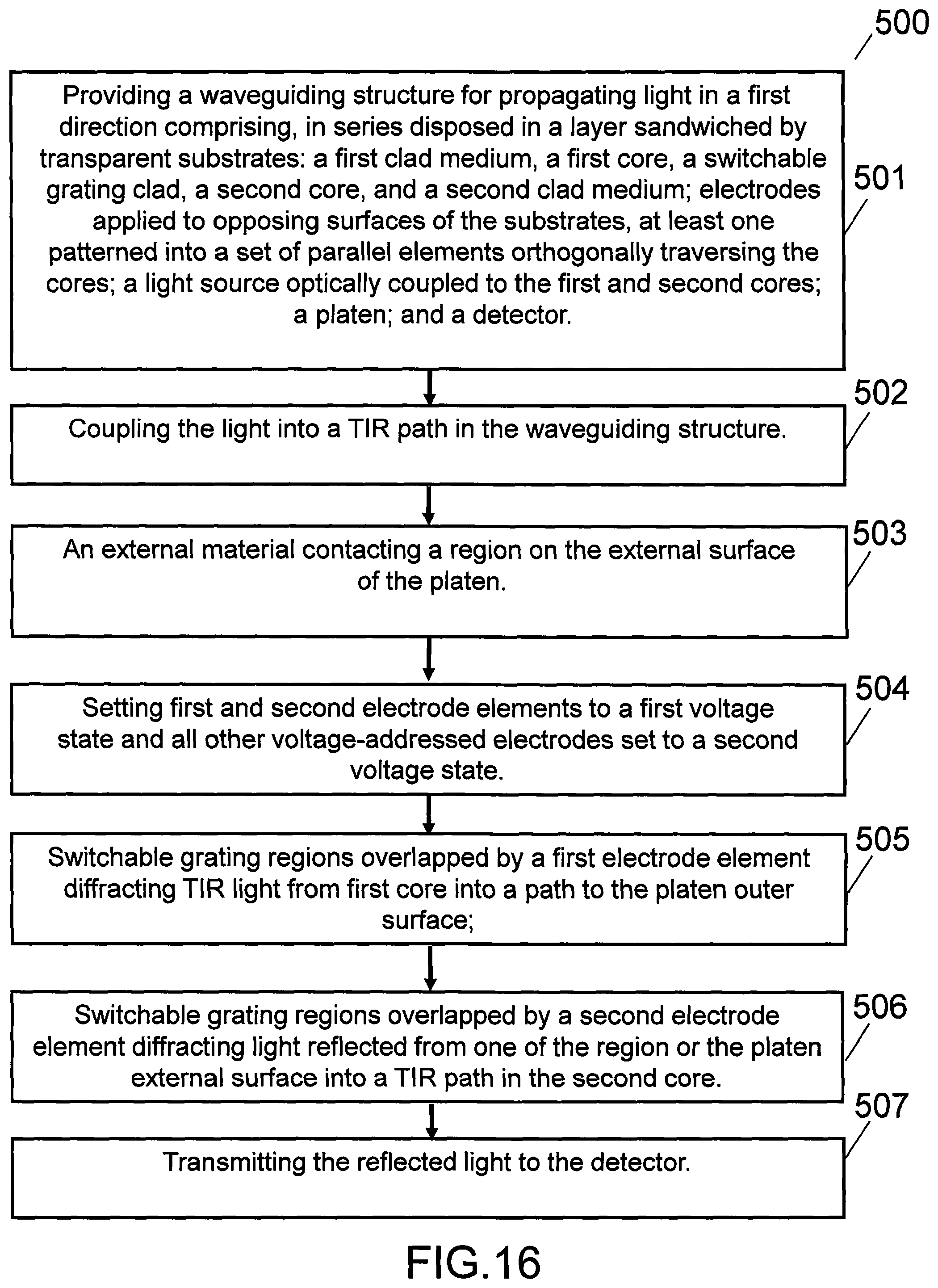
D00013
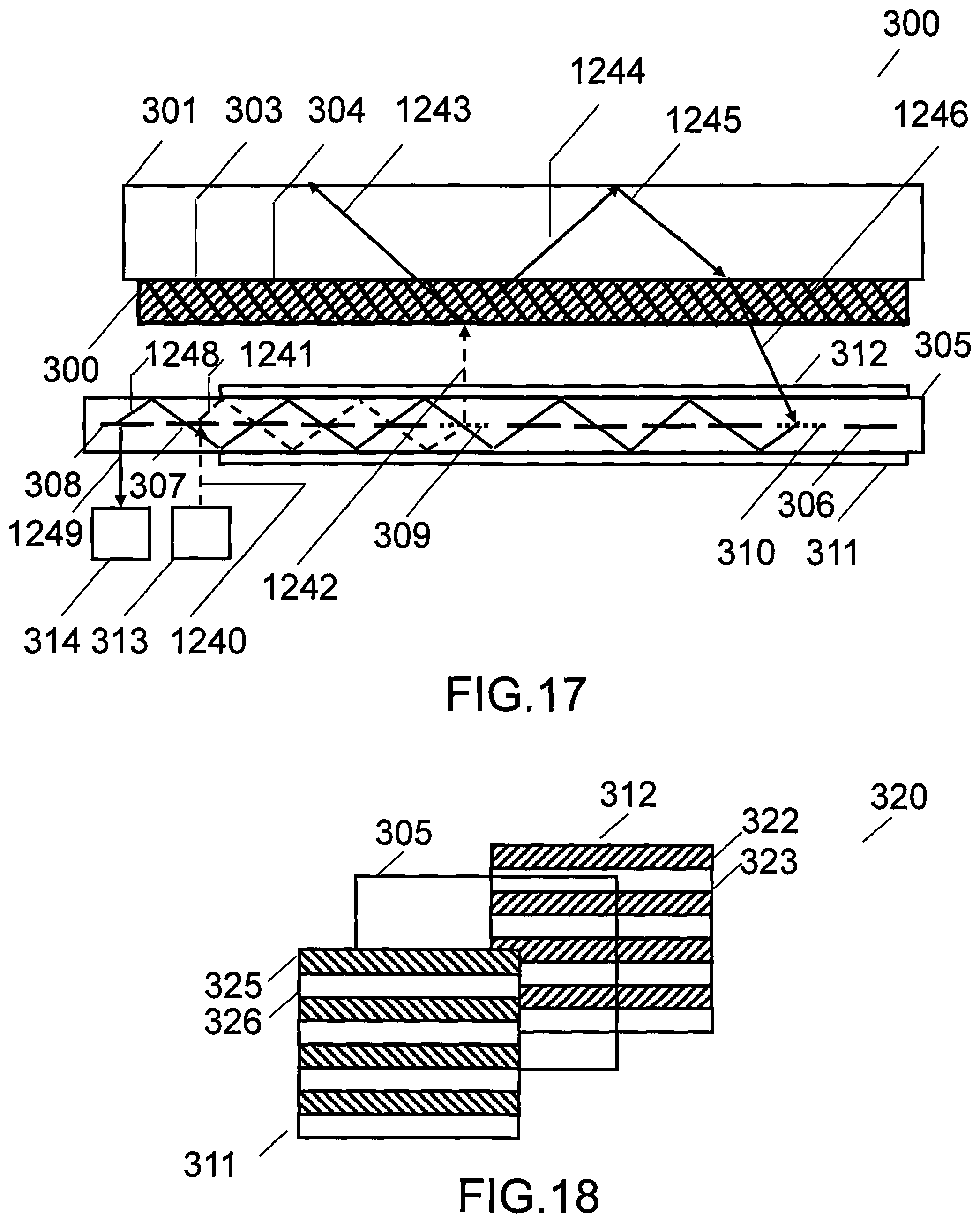
D00014
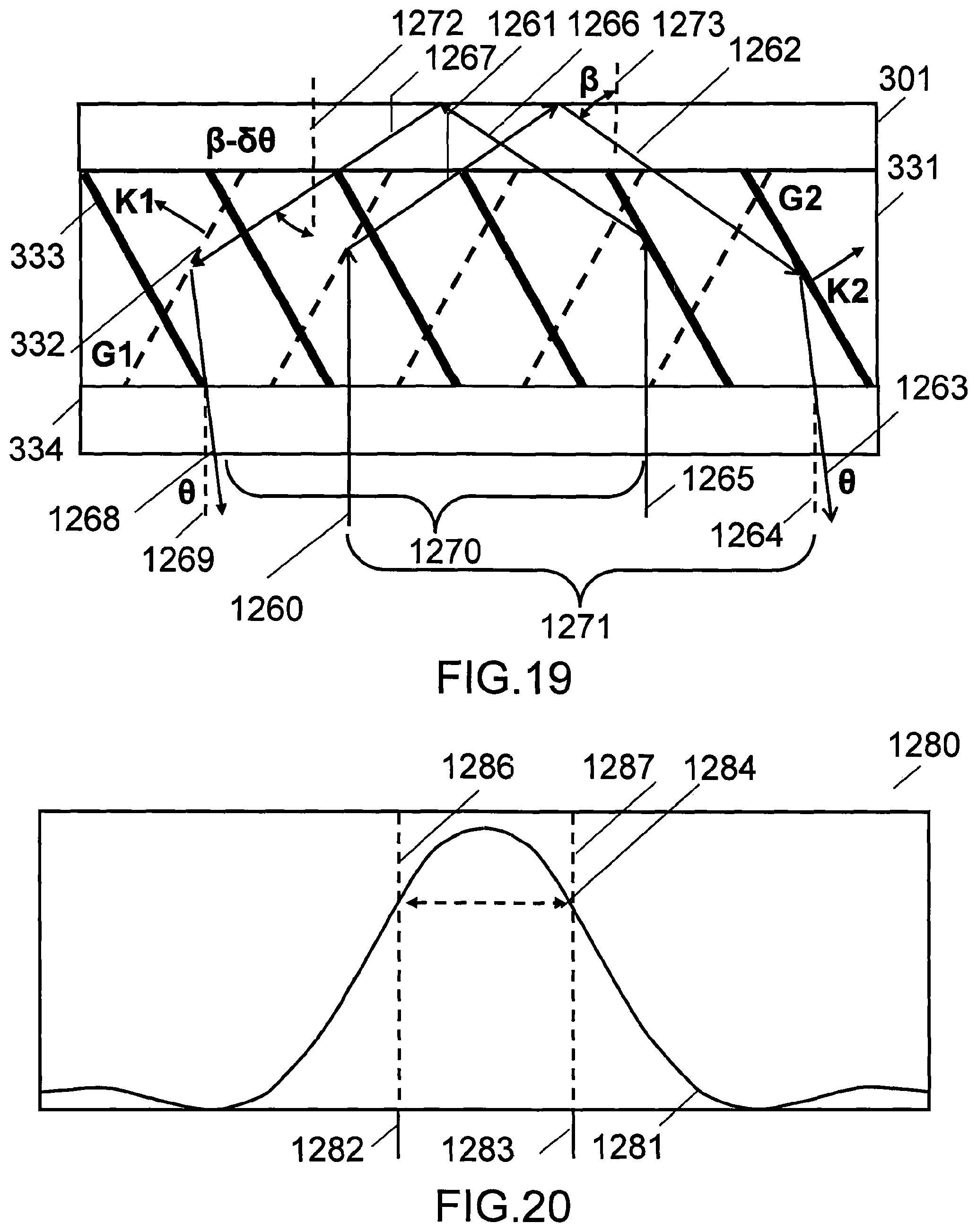
XML
uspto.report is an independent third-party trademark research tool that is not affiliated, endorsed, or sponsored by the United States Patent and Trademark Office (USPTO) or any other governmental organization. The information provided by uspto.report is based on publicly available data at the time of writing and is intended for informational purposes only.
While we strive to provide accurate and up-to-date information, we do not guarantee the accuracy, completeness, reliability, or suitability of the information displayed on this site. The use of this site is at your own risk. Any reliance you place on such information is therefore strictly at your own risk.
All official trademark data, including owner information, should be verified by visiting the official USPTO website at www.uspto.gov. This site is not intended to replace professional legal advice and should not be used as a substitute for consulting with a legal professional who is knowledgeable about trademark law.