Method and Apparatus for Providing a Polarization Selective Holographic Waveguide Device
Popovich; Milan Momcilo ; et al.
U.S. patent application number 16/086578 was filed with the patent office on 2019-04-25 for method and apparatus for providing a polarization selective holographic waveguide device. This patent application is currently assigned to DigiLens, Inc.. The applicant listed for this patent is DigiLens, Inc.. Invention is credited to Alastair John Grant, Milan Momcilo Popovich, Jonathan David Waldern.
| Application Number | 20190121027 16/086578 |
| Document ID | / |
| Family ID | 58633026 |
| Filed Date | 2019-04-25 |


View All Diagrams
| United States Patent Application | 20190121027 |
| Kind Code | A1 |
| Popovich; Milan Momcilo ; et al. | April 25, 2019 |
Method and Apparatus for Providing a Polarization Selective Holographic Waveguide Device
Abstract
A waveguide apparatus, comprises: disposed in at least one layer: an input coupler; a first fold grating; a second fold grating; an output coupler; and a source of light optically coupled to the waveguide providing at least first and second polarizations of the light and at least one wavelength. The input coupler is configured to cause the first polarization light to travel along a first total internal reflection (TIR) path and the second polarization light to travel along a second TIR path.
| Inventors: | Popovich; Milan Momcilo; (Leicester, GB) ; Waldern; Jonathan David; (Los Altos Hills, CA) ; Grant; Alastair John; (San Jose, CA) | ||||||||||
| Applicant: |
|
||||||||||
|---|---|---|---|---|---|---|---|---|---|---|---|
| Assignee: | DigiLens, Inc. Sunnyvale CA |
||||||||||
| Family ID: | 58633026 | ||||||||||
| Appl. No.: | 16/086578 | ||||||||||
| Filed: | March 23, 2017 | ||||||||||
| PCT Filed: | March 23, 2017 | ||||||||||
| PCT NO: | PCT/GB2017/000040 | ||||||||||
| 371 Date: | September 19, 2018 |
Related U.S. Patent Documents
| Application Number | Filing Date | Patent Number | ||
|---|---|---|---|---|
| 62391333 | Apr 27, 2016 | |||
| 62390271 | Mar 24, 2016 | |||
| Current U.S. Class: | 1/1 |
| Current CPC Class: | G02B 27/017 20130101; G02B 6/2726 20130101; G02B 27/286 20130101; G02B 6/34 20130101; G02B 6/2773 20130101; G02B 27/283 20130101; G02B 27/0081 20130101 |
| International Class: | G02B 6/27 20060101 G02B006/27; G02B 6/34 20060101 G02B006/34; G02B 27/28 20060101 G02B027/28 |
Claims
1. A waveguide apparatus, comprising: disposed in at least one layer: as input coupler; a first fold grating; a second fold grating; an output coupler; and a source of light optically coupled to said waveguide providing at least first and second polarizations of said light and at least one wavelength, wherein said input coupler is configured to cause said first polarization light to travel along a first total internal reflection (TIR) path and said second polarization light to travel along a second TIR path.
2. The apparatus of claim 1 wherein said first fold grating is configured to cause said first polarization light in said first TIR path to travel along a third TIR paths to said output coupler, wherein said output coupler directs said third TIR path out of said waveguide.
3. The apparatus of claim 1 wherein said input coupler comprises first and second gratings for coupling said first and second polarization light or color into said first and second TIR paths, wherein said first and second gratings are configured as a stack or multiplexed in a single layer.
4. The apparatus of claim 1 wherein said output coupler comprises third and fourth gratings coupling said third and fourth paths out of said waveguide, wherein said first and second gratings are configured as a stack or multiplexed in a single layer.
5. The apparatus of claim 1 wherein said fold grating is configured to provide pupil expansion in a first direction, wherein said output grating is configured to provide pupil expansion in a second direction different than said first direction.
6. The apparatus of claim 1 wherein at least one of said input coupler, said fold grating or said output grating is a rolled k-vector grating.
7. The apparatus of claim 1 wherein said light undergoes a dual interaction within at least one of said fold gratings.
8. The apparatus of claim 1, wherein said source, a microdisplay for displaying image pixels and collimation optics, and wherein said IIN projects the image displayed on said microdisplay panel such that each image pixel is converted into a unique angular direction within said first waveguide
9. The apparatus of claim 1, wherein said waveguide provides one of a HMD, a HUD, an eye-slaved display, a dynamic focus display or a light field display.
10. The apparatus of claim 1, wherein at least one of said input coupler, fold grating and output grating multiplexes at least one of color or angle.
11. The apparatus of claim 1 comprising at least one grating with spatially varying pitch.
12. The apparatus of claim 1 wherein said at least one grating layer comprises a first grating layer operating at a first wavelength and a second grating layer operating at a second wavelength.
13. The apparatus of claim 1 configured to operate in the infrared.
14. The apparatus of claim 1 wherein said output coupler couples light from said waveguide onto a detector.
15. The apparatus of claim 1, wherein at least one of said input coupler, said fold grating, and said output grating is one of a switchable Bragg grating recorded in a holographic photopolymer a HPDLC material or a uniform modulation holographic liquid crystal polymer material or a surface relief grating.
16. The apparatus of claim 1 wherein said first and second polarizations are orthogonal.
17. A method of propagating light of more than one polarization component comprising the steps of: a) providing a waveguide containing an input grating comprising crossed first and second gratings. b) coupling a source of light to said waveguide. c) said first grating diffracting a first polarization state of light into a first waveguide path. d) said second grating diffracting a second polarization state of light into a second waveguide path.
18. A method of propagating light of more than one polarization component comprising the steps of: a) providing a waveguide containing an input grating comprising crossed first and second gratings; first and second fold gratings; and an output grating comprising crossed third and fourth gratings; b) coupling a source of light to said waveguide; c) said first grating diffracting a first polarization state of said light into a first waveguide path; d) said first grating diffracting a second polarization state of said light into a second waveguide path; e) said first fold grating diffracting light from said first waveguide path into a third waveguide path to said output grating; f) said second fold grating diffracting light in said second waveguide path into a fourth waveguide path to said output grating; g) said third grating diffracting light in said third waveguide path out of said waveguide; h) said fourth grating diffracting light in said fourth waveguide path out of said waveguide.
19. A method of propagating light of more than one polarization component comprising the steps of: a) providing a waveguide containing an input grating comprising crossed first and second gratings; first and second fold gratings; and an output grating comprising crossed third and fourth gratings; b) coupling a source of light of first and second colors to said waveguide; c) said first grating diffracting a first color, first polarization state of said light into said first waveguide path; d) said first grating diffracting a second color, second polarization state of said light into a second waveguide path; e) said first fold grating diffracting light from said first waveguide path into a third waveguide path to said output grating; f) said second fold grating diffracting light in said second waveguide path into a fourth waveguide path to said output grating; g) said third grating diffracting light in said third waveguide path out of said waveguide; h) said fourth grating diffracting light in said fourth waveguide path out of said waveguide.
20. A method of propagating light of more than one polarization component comprising the steps of: a) providing a waveguide comprising a first substrate containing an input grating comprising crossed first and second gratings, first and second fold gratings, and an output grating comprising crossed third and fourth gratings; a second substrate containing an input grating comprising crossed fifth and sixth gratings; and a half wave retarder film sandwiched by the input gratings; b) coupling a source of light of first and second colors to said waveguide; c) said the first and fifth gratings diffracting a first color, first polarization state of said light into a first waveguide path; d) said second and sixth gratings diffracting a second color, second polarization state of said light into a second waveguide path; e) said first fold grating diffracting light in said first waveguide path into a third waveguide path to said output grating; f) said second fold grating diffracting light in said second waveguide path into a fourth waveguide path to said output grating; g) said third grating diffracting light in said third waveguide path out of said waveguide; h) said fourth grating diffracting light in said fourth waveguide path out of said waveguide.
Description
CROSS-REFERENCE TO PRIORITY APPLICATIONS
[0001] This application is a U.S. national stage of PCT Application No. PCT/GB2017/000040 entitled METHOD AND APPARATUS FOR PROVIDING A POLARIZATION SELECTIVE HOLOGRAPHIC WAVEGUIDE DEVICE filed on Mar. 23, 2017, which claims the benefit of U.S. Provisional Application No. 62/390,271 entitled HOLOGRAPHIC WAVEGUIDE DEVICES FOR USE WITH UNPOLARIZED LIGHT filed on Mar. 24, 2016 and U.S. Provisional Application No. 62/391,333 entitled METHOD AND APPARATUS FOR PROVIDING A POLARIZATION SELECTIVE HOLOGRAPHIC WAVEGUIDE DEVICE filed on Apr. 21, 2016, the disclosures of which are hereby incorporated by reference in their entireties.
BACKGROUND OF THE INVENTION
[0002] The present disclosure relates to waveguide devices and more particularly to a holographic waveguide device for use with unpolarized light.
[0003] Waveguide optics is currently being considered for a range of display and sensor applications for which the ability of waveguides to integrate multiple optical functions into a thin, transparent, lightweight substrate is of key importance. This sew approach is stimulating new product developments including near-eye displays for Augmented Reality (AR) and Virtual Reality (VR), compact Heads Up Display (HUDs) for aviation and road transport and sensors for biometric and laser radar (LIDAR) applications. Waveguide displays have been proposed which use diffraction gratings to preserve eye box size while reducing lens size. U.S. Pat. No. 4,309,070 issued to St. Leger Searle and U.S. Pat. No. 4,711,512 issued to Upatnieks disclose substrate waveguide head up displays where the pupil of a collimating optical system is effectively expanded by the waveguide structure. U.S. patent application Ser. No. 13/869,866 discloses holographic wide angle displays. Waveguides have also been proposed for sensor applications such as eye tracking, finger print scanning and LIDAR. The advantages of Bragg gratings (also referred to as a volume grating), in waveguide applications are well known. Bragg gratings have high efficiency with little light being diffracted into higher orders. The relative amount of light in the diffracted and zero order can be varied by controlling the refractive index modulation of the grating, a property which is used to make lossy waveguide gratings for extracting light over a large pupil. One important class of gratings is known as Switchable Bragg Gratings (SBG). SBGs are fabricated by first placing a thin film of a mixture of photopolymerizable monomers and liquid crystal material between parallel glass plates. One or both glass plates support electrodes, typically transparent indium tin oxide films, for applying an electric field across the film. A volume phase grating is then recorded by illuminating the liquid material (often referred to as the syrup) with two mutually coherent laser beams, which interfere to form a slanted fringe grating structure. During the recording process, the monomers polymerize and the mixture undergoes a phase separation, creating regions densely populated by liquid crystal micro-droplets, interspersed with regions of clear polymer. The alternating liquid crystal-rich and liquid crystal-depleted regions form the fringe planes of the grating. The resulting volume phase grating can exhibit very high diffraction efficiency, which may be controlled by the magnitude of the electric field applied across the film. When an electric field is applied to the grating via transparent electrodes, the natural orientation of the LC droplets is changed causing the refractive index modulation of the fringes to reduce and the hologram diffraction efficiency to drop to very low levels. Typically, SBG Elements are switched clear in 30 .mu.s. With a longer relaxation time to switch ON. Note that the diffraction efficiency of the device can be adjusted, by means of the applied voltage, over a continuous range. The device exhibits near 100% efficiency with no voltage applied and essentially zero efficiency with a sufficiently high voltage applied. In certain types of HPDLC devices magnetic fields may be used to control the LC orientation. In certain types of HPDLC phase separation of the LC material from the polymer may be accomplished to such a degree that no discernible droplet structure results. A SBG may also be used as a passive grating. In this mode its chief benefit is a uniquely high refractive index modulation.
[0004] SBGs may be used to provide transmission or reflection gratings for free space applications. SBGs may be implemented as waveguide devices in which the HPDLC forms either the waveguide core or an evanescently coupled layer in proximity to the waveguide. The parallel glass plates used to form the HPDLC cell provide a total internal reflection (TIR) light guiding structure. Light is coupled out of the SBG when the switchable grating diffracts the light at an angle beyond the TIR condition. Waveguides are currently of interest in a range of display and sensor applications. Although much of the earlier work on HPDLC has been directed at reflection holograms transmission devices are proving to be much more versatile as optical system building blocks. Typically, the HPDLC used in SBGs comprise liquid crystal (LC), monomers, photoinitiator dyes, and coinitiators. The mixture frequently includes a surfactant. The patent and scientific literature contains many examples of material systems and processes that may be used to fabricate SBGs. Two fundamental patents are: U.S. Pat. No. 5,942,157 by Sutherland, and U.S. Pat. No. 5,751,452 by Tanaka et al. Both filings describe monomer and liquid crystal material combinations suitable for fabricating SBG devices. One of the known attributes of transmission SBGs is that the LC molecules tend to align normal to the grating fringe planes. The effect of the LC molecule alignment is that transmission SBGs efficiently diffract P polarized light (that is, light with the polarization vector in the plane of incidence) but have nearly zero diffraction efficiency for S polarized light (that is, light with the polarization vector normal to the plane of incidence. Transmission SBGs may not be used at near-grazing incidence as the diffraction efficiency of any grating for P polarization falls to zero when the included angle between the incident and reflected light is small. The switching capability of SBGs can be exploited in a range of sensors including eye trackers, LIDAR and fingerprint scanners. Switchable Bragg gratings (SBGs) may be used in waveguides to eliminate extra layers and to reduce the thickness of current display systems, including HMDs, HUDs, and other near eye displays and to increase the field of view by tiling images presented sequentially on a microdisplay.
[0005] The polarization selectivity of SBGs results to a 50% light throughput loss when LEDs are used as a light source. While it is possible in theory to recover some of the lost light using polarization components this tends to be difficult in practice due to optical inefficiencies.
[0006] There is a requirement for a low cost, efficient, compact holographic waveguide for use with unpolarized light.
SUMMARY OF THE INVENTION
[0007] It is a first object of the invention to provide a low cost, efficient, compact holographic waveguide for use with unpolarized light.
[0008] The objects of the invention are met in a first embodiment in which a waveguide apparatus, comprises: disposed in at least one layer: an input coupler; a first fold grating; a second fold grating; an output coupler; and a source of light optically coupled to the waveguide providing at least first and second polarizations of the light and at least one wavelength. The input coupler is configured to cause the first polarization light to travel along a first total internal reflection (TIR) path and the second polarization light to travel along a second TIR path.
[0009] In some embodiments, the first fold grating is configured to cause the first polarization light in the first TIR path to travel along a third TIR paths to the output coupler, wherein the output coupler directs the third TIR path out of the waveguide.
[0010] In some embodiments, the input coupler comprises first and second gratings for coupling the first and second polarization light or color into the first and second TIR paths, wherein the first and second gratings are configured as a stack or multiplexed in a single layer.
[0011] In some embodiments, the output coupler comprises third and fourth gratings coupling the third and fourth paths out of the waveguide, wherein the first and second gratings are configured as a stack or multiplexed in a single layer.
[0012] In some embodiments, the fold grating is configured to provide pupil expansion in a first direction, wherein the output grating is configured to provide pupil expansion in a second direction different than the first direction.
[0013] In some embodiments, at least one of the input coupler, the fold grating or the output grating is a rolled k-vector grating.
[0014] In some embodiments, the light undergoes a dual interaction within at least one of the fold gratings.
[0015] In some embodiments, the source, a microdisplay for displaying image pixels and collimation optics, and wherein the IIN projects the image displayed on the microdisplay panel such that each image pixel is converted into a unique angular direction within the first waveguide.
[0016] In some embodiments, the waveguide provides one of a HMD, a HUD, an eyes-slaved display, a dynamic focus display or a light field display.
[0017] In some embodiments, at least one of the input coupler, fold grating and output grating multiplexes at least one of color or angle.
[0018] In some embodiments, the apparatus comprises at least one grating with spatially varying pitch.
[0019] In some embodiments, the at least one grating layer comprises a first grating layer operating at a first wavelength and a second grating layer operating at a second wavelength.
[0020] In some embodiments, the apparatus is configured to operate in the infrared.
[0021] In some embodiments, the output coupler couples light from the waveguide onto a detector.
[0022] In some embodiments, at least one of the input coupler, the fold grating, and the output grating is one of a switchable Bragg grating recorded in a holographic photopolymer a HPDLC material or a uniform modulation holographic liquid crystal polymer material or a surface relief grating.
[0023] In some embodiments, the first and second polarizations are orthogonal.
[0024] In some embodiments, there is provided a method of propagating light of more than one polarization component comprising the steps of: [0025] a) providing a waveguide containing an input grating comprising crossed first and second gratings. [0026] b) coupling a source of light to the waveguide. [0027] c) the first grating diffracting a first polarization state of light into a first waveguide path. [0028] d) the second grating diffracting a second polarization state of light into a second waveguide path.
[0029] In some embodiments, there is provided a method of propagating light of more than one polarization component comprising the steps of: [0030] a) providing a waveguide containing an input grating comprising crossed first and second gratings; first and second fold gratings; and an output grating comprising crossed third and fourth gratings; [0031] b) coupling a source of light to the waveguide; [0032] c) the first grating diffracting a first polarization state of the light into a first waveguide path; [0033] d) the first grating diffracting a second polarization state of the light into a second waveguide path; [0034] e) the first fold grating diffracting light from the first waveguide path into a third waveguide path to the output grating; [0035] f) the second fold grating diffracting light in the second waveguide path into a fourth waveguide path to the output grating; [0036] g) the third grating diffracting light in the third waveguide path out of the waveguide; [0037] h) the fourth grating diffracting light in the fourth waveguide path out of the waveguide.
[0038] In some embodiments, there is provided a method of propagating light of more than one polarization component comprising the steps of: [0039] a) providing a waveguide containing an input grating comprising crossed first and second gratings; first and second fold gratings; and an output grating comprising crossed third and fourth gratings; [0040] b) coupling a source of light of first and second colors to the waveguide; [0041] c) the first grating diffracting a first color, first polarization state of the light into the first waveguide path; [0042] d) the first grating diffracting a second color, second polarization state of the light into a second waveguide path; [0043] e) the first fold grating diffracting light from the first waveguide path into a third waveguide path to the output grating; [0044] f) the second fold grating diffracting light in the second waveguide path into a fourth waveguide path to the output grating; [0045] g) the third grating diffracting light in the third waveguide path out of the waveguide; [0046] h) the fourth grating diffracting light in the fourth waveguide path out of the waveguide.
[0047] In some embodiments, there is provided a method of propagating light of more than one polarization component comprising the steps of: [0048] a) providing a waveguide comprising a first substrate containing an input grating comprising crossed first and second gratings, first and second fold gratings, and an output grating comprising crossed third and fourth gratings; a second substrate containing an input grating comprising crossed fifth and sixth gratings; and a half wave retarder film sandwiched by the input gratings; [0049] b) coupling a source of light of first and second colors to the waveguide; [0050] c) the the first and fifth gratings diffracting a first color, first polarization state of the light into a first waveguide path; [0051] d) the second and sixth gratings diffracting a second color, second polarization state of the light into a second waveguide path; [0052] e) the first fold grating diffracting light in the first waveguide path into a third waveguide path to the output grating; [0053] f) the second fold grating diffracting light in the second waveguide path into a fourth waveguide path to the output grating; [0054] g) the third grating diffracting light in the third waveguide path out of the waveguide; [0055] h) the fourth grating diffracting light in the fourth waveguide path out of the waveguide.
[0056] Following below are more detailed descriptions of various concepts related to, and embodiments of, an inventive holographic waveguide for use with unpolarized light. It should be appreciated that various concepts introduced above and discussed in greater detail below may be implemented in any of numerous ways, as the disclosed concepts are not limited to any particular manner of implementation. Examples of specific implementations and applications are provided primarily for illustrative purposes. A more complete understanding of the invention can be obtained by considering the following detailed description in conjunction with the accompanying drawings, wherein like index numerals indicate like parts. For purposes of clarity, details relating to technical material that is known in the technical fields related to the invention have not been described in detail.
BRIEF DESCRIPTION OF THE DRAWINGS
[0057] FIG. 1 is a schematic plan view of a waveguide device in a first embodiment.
[0058] FIG. 2A is a schematic three-dimensional view of the input grating of the first embodiment.
[0059] FIG. 2B is grating slant angle in the input grating of the first embodiment.
[0060] FIG. 3 is a schematic cross section view of the waveguide device in the first embodiment.
[0061] FIG. 4 is a cross section view of a rolled K-vector grating used in one embodiment.
[0062] FIG. 5 is a cross section view of a rolled K-vector grating used in one embodiment.
[0063] FIG. 6 is a schematic plan view of a waveguide device in one embodiment.
[0064] FIG. 7 is a schematic plan view of a waveguide device in one embodiment.
[0065] FIG. 8 is a schematic plan view of a waveguide device in which the input and output grating devices each combining three separate gratings in one embodiment.
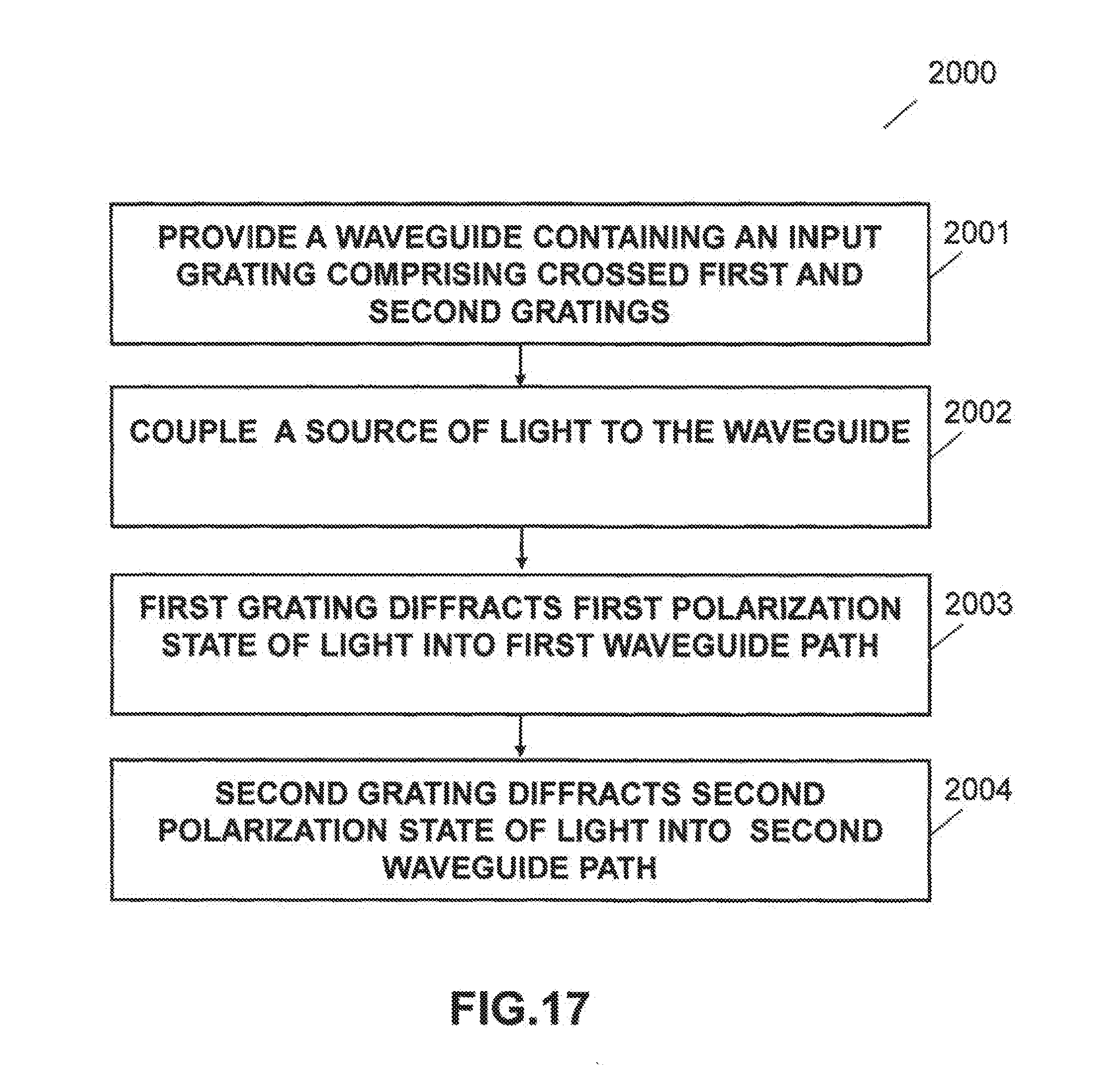
[0066] FIG. 9 is a schematic plan view of waveguide gratings in one embodiment.
[0067] FIG. 10 is a schematic cross section view of a waveguide device including polarization control layers in one embodiment.
[0068] FIG. 11 is a schematic cross section view of a two-grating layer waveguide device in one embodiment.
[0069] FIG. 12 is a schematic cross section view of a waveguide device comprising two waveguides each containing a grating layer in one embodiment.
[0070] FIG. 13 is a schematic plan view of a color waveguide device in one embodiment.
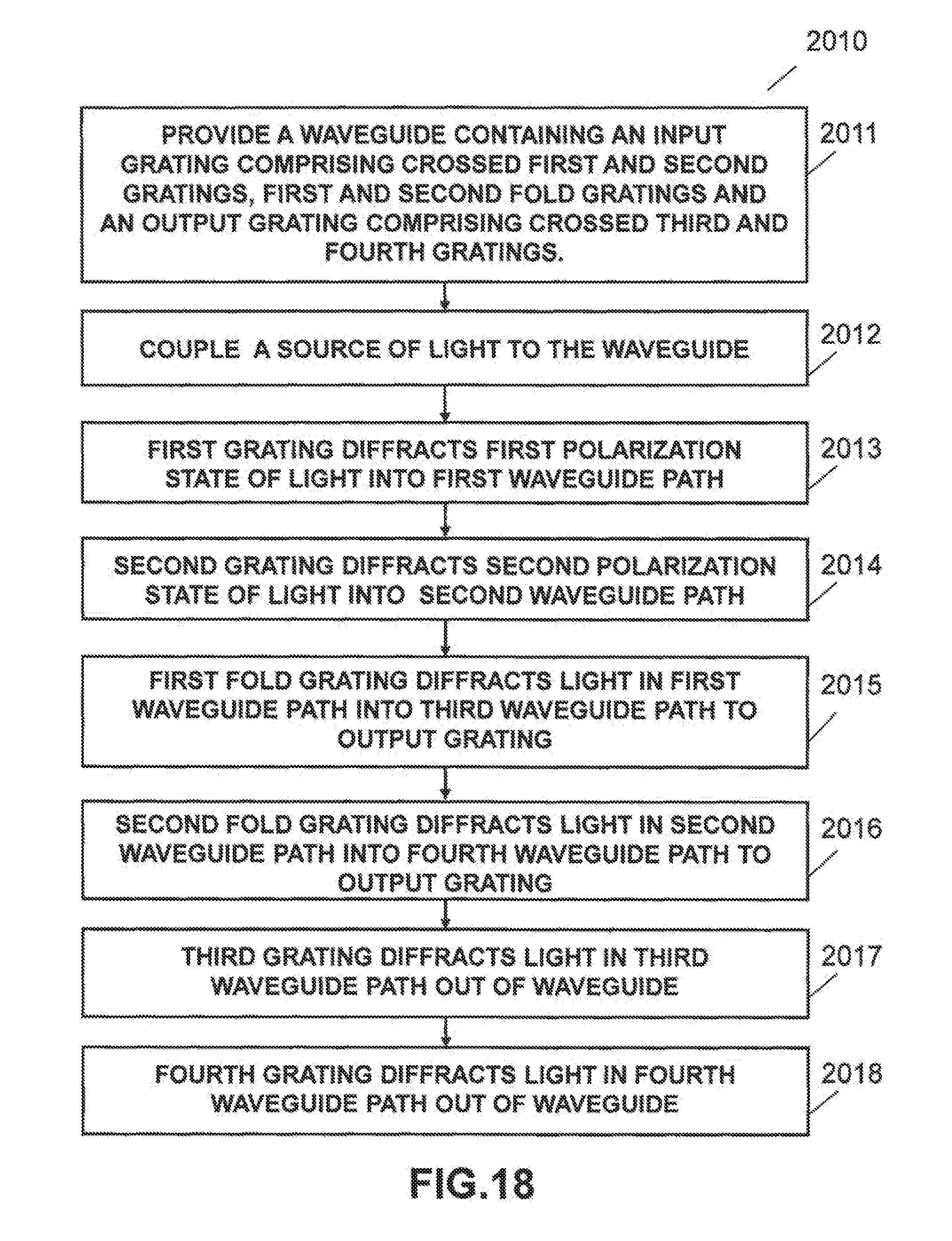
[0071] FIG. 14 is a schematic cross section view of a color waveguide device in one embodiment.
[0072] FIG. 15 is a schematic plan view of a substrate used in a color waveguide device including a polarization recovery layer in one embodiment.
[0073] FIG. 16 is a schematic cross section view of a color waveguide device including a polarization recovery layer in one embodiment.
[0074] FIG. 17 is a flow diagram illustrating a method of coupling light of more than one polarization component into a waveguide in one embodiment.
[0075] FIG. 18 is a flow diagram illustrating a method of coupling light of more than one polarization component into a waveguide in one embodiment.
[0076] FIG. 19 is a flow diagram illustrating a method of coupling light of more than one polarization component and more than one color into a waveguide in one embodiment.
[0077] FIG. 20 is a flow diagram illustrating a method of coupling light of more than one polarization component and more than one color into a waveguide with polarization recovery in one embodiment.
DETAILED DESCRIPTION OF THE INVENTION
[0078] The invention will now be further described by way of example only with reference to the accompanying drawings. It will apparent to those skilled in the art that the present invention may be practiced with some or all of the present invention as disclosed in the following description. For the purposes of explaining the invention well-known features of optical technology known to those skilled in the art of optical design and visual displays have been omitted or simplified in order not to obscure the basic principles of the invention. Unless otherwise stated the term "on-axis" in relation to a ray or a beam direction refers to propagation parallel to an axis normal to the surfaces of the optical components described in relation to the invention. In the following description the terms light, ray, beam and direction may be used interchangeably and in association with each other to indicate the direction of propagation of electromagnetic radiation along rectilinear trajectories. The term light and illumination may be used in relation to the visible and infrared bands of the electromagnetic spectrum. Parts of the following description will be presented using terminology commonly employed by those skilled in the art of optical design. It should also be noted that in the following description of the invention repeated usage of the phrase "in one embodiment" does not necessarily refer to the same embodiment. Referring generally to the Figures, systems and methods relating to displays or sensors are shown according to various embodiments.
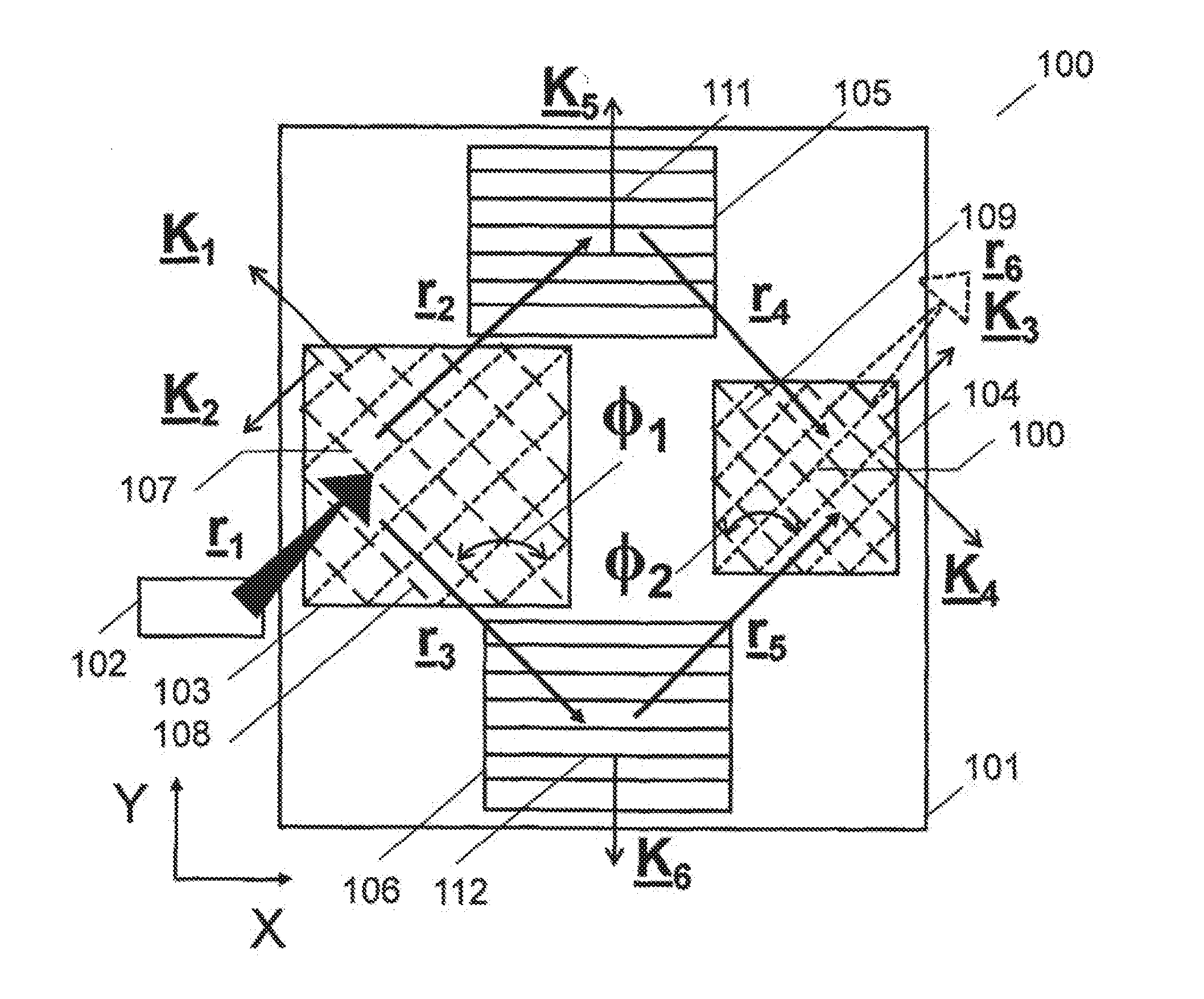
[0079] The object of the invention is achieved in first embodiment 100 illustrated in FIG. 1 in which there is provided a waveguide device comprising a waveguide 101 which contains an Input grating 103 an output grating 104 and fold grating exit pupil expanders 105,106. The input grating receives light from an external light source 102 in the direction indicated by the vector r.sub.1. In some embodiments, the external light will be unpolarized. As will be discussed later, in display applications of the invention the light source will comprise as input image node (IIN) providing image-modulated light. In displays applications of the invention the input grating would normally be configured to receive collimated light from the IIN and to cause the light to travel within the waveguide via total internal reflection between the first surface and the second surface to the fold grating.
[0080] As used herein, the term grating may encompass a grating comprised of a set of gratings in some embodiments. For example, in some embodiments the input grating and output grating each comprise two or more gratings multiplexed into a single layer. It is well established in the literature of holography that more than one holographic prescription can be recorded into a single holographic layer. Methods for recording such multiplexed holograms are well known to those skilled in the art. In some embodiments the input grating and output grating may each comprise two overlapping gratings layers that are in contact or vertically separated by one or more thin optical substrate. In some embodiments the grating layers are sandwiched between glass or plastic substrates. In some embodiments two or more such gratings layers may form a slack within which total internal reflection occurs at the outer substrate and air interfaces. In some embodiments the waveguide may comprise just one grating layer. In some embodiments electrodes may be applied to faces of the substrates to switch gratings between diffracting and clear states. The stack may further comprise additional layers such as beam splitting coatings and environmental protection layers. The input and output gratings shown FIG. 1 may be provided by any of the above described grating configurations. Advantageously, the input and output gratings are designed to have common surface grating pitch.
[0081] An important feature of the input gratings used in the invention is that they combine gratings orientated such that each grating diffracts a particular polarization of the incident unpolarized light into a waveguide path. The output gratings are configured in a similar fashion so the light from the waveguide paths is combined and coupled out of the waveguide as unpolarized light. In the embodiment of FIG. 1 the input grating and output grating each combine crossed gratings with peak diffraction efficiency for orthogonal polarizations states. In some embodiments, the polarization states are S-polarized and P-polarized. In some embodiments, the polarization states are opposing senses of circular polarization. In some embodiments, more than two gratings each operating on a predefined polarization state may be combined. The advantage of gratings recorded in liquid crystal polymer systems, such as SBGs, in this regard is that owing to their inherent birefringence they exhibit strong polarization selectivity. However, other grating technologies that can be configured to provide unique polarization states may be used. Each grating is characterized by a grating vector (or K-vector) in 3D space which in the case of a Bragg grating is defined as the vector normal to the Bragg fringes. The grating vector determines the optical efficiency for a given range of input and diffracted angles.
[0082] In FIG. 1 the input grating is formed from the crossed slant gratings 107,108 having grating vectors K.sub.1,K.sub.2, with the grating fringes being rotated in the waveguide plane (or clocked) at the relative angle .PHI..sub.1 and the output grating is formed from the crossed slant gratings 109,110 having grating vectors K.sub.3,K.sub.4, with the grating fringes being rotated in the waveguide plane (or clocked) at the relative angle .PHI..sub.2. The fold gratings contain the slant gratings 111,112 having grating vectors K.sub.5,K.sub.6. In some embodiments, the angles .PHI..sub.1 and .PHI..sub.2 are each equal to 90 degrees. In some embodiments, the angles .PHI..sub.1 and .PHI..sub.2 may be less than 90 degrees. A first polarization component of the input light incident on the input grating along the direction r.sub.1 is directed by the grating 107 into a TIR path along the direction r.sub.2 and second polarization component is directed by the second grating 108 into a second TIR path along the direction r.sub.3. The light along the paths r.sub.2, r.sub.3 and is expanded (in the XY plane of the drawing) by the fold gratings 105,106 and diffracted into the TIR paths r.sub.4 and r.sub.3 towards the output grating. FIG. 2 is a three-dimensional view of the input grating of FIG. 1. FIG. 2A shows a detail of one embodiment in which multiplexed gratings are used in the input grating. FIG. 2A show four grating fringes 120 of the grating 108 and four grating fringes 121 of the grating 107. FIG. 2B shows a cross sectional view in the plane X'Y' containing the grating vector K.sub.3 in which one fringe 122 is illustrated indicated the grating slant angle .theta..sub.1. In some embodiments, the gratings in the input grating have identical slant angles and grating pitches. In some embodiments, the grating layout and beam propagation paths illustrated in in FIG. 1 are symmetrical about the X axis.
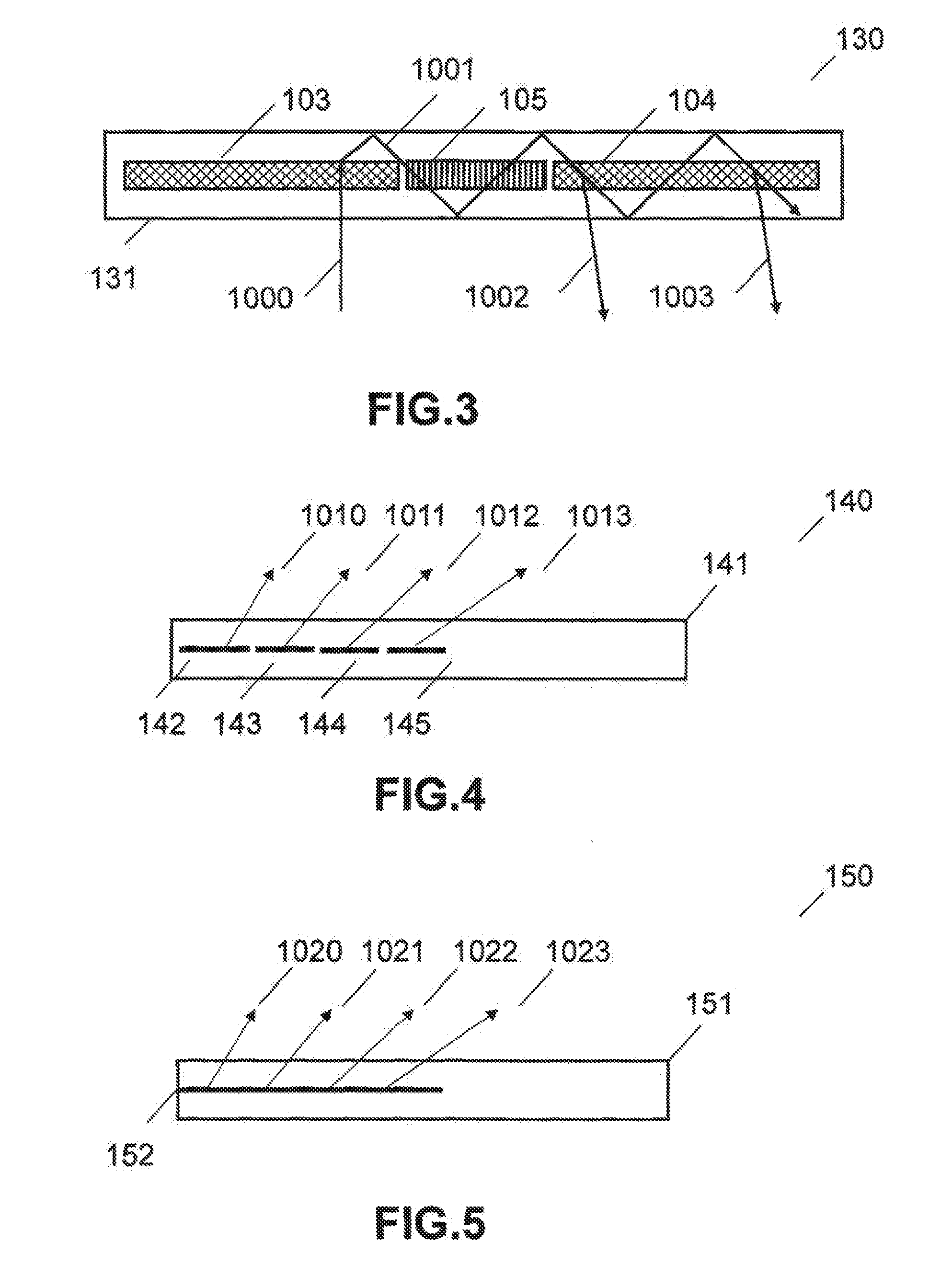
[0083] FIG. 3 is a cross section 130 of the waveguide device of FIG. 1 showing the waveguide 131, input grating 103, the output grating 104 and one of the fold gratings 105. Input rays 1000, the total internal reflection (TIR) path 1001 between the input grating and output grating and rays 1002,1003 out-coupled from the waveguide by the output grating are illustrated.
[0084] In some embodiments, the fold gratings are clocked (that is, tilted in the waveguide plane) at 45.degree. to the X or Y axes to ensure adequate angular bandwidth for the folded light. However, some embodiments of the invention may use other clock angles to satisfy spatial constraints on the positioning of the gratings that may arise in the ergonomic design of the display.
[0085] In the embodiment of FIG. 1 each grating has a feed K vector. In some embodiments, at least one of the input and output gratings have rolled k-vectors. Rolling the K-vectors allows the angular band width of the grating to be expanded without the need to increase the waveguide thickness. FIG. 4 illustrates a rolled K-vector grating 140 comprises a waveguide portion 141 containing the discrete grating elements 142-145 having K-vectors 1010-1013. In some embodiments such as the one illustrated in FIG. 5 a rolled K-vector grating comprises a waveguide portion 151 containing a single grating element 152 within which the K-vectors undergo a smooth monotonic variation in direction including the illustrated directions 1020-1023. Rolled K-vector gratings of the type illustrated in FIGS. 4-5 can be implement in any of the gratings discussed above.
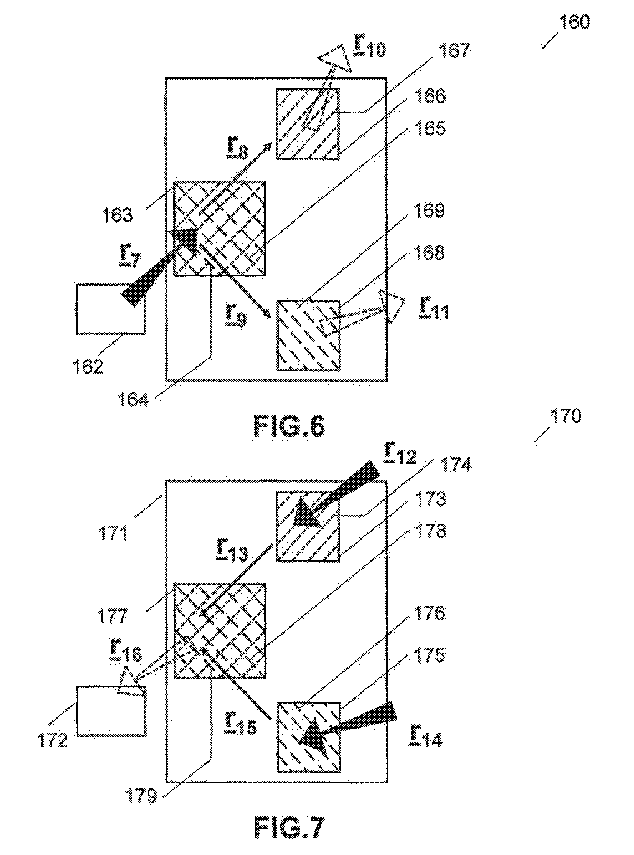
[0086] The principles and teachings of the invention in combination with other waveguide inventions by the inventors as disclosed in the reference documents incorporated by reference herein may be applied in many different display and sensor devices. In some embodiments based on the embodiment in FIG. 6 a waveguide device 160 comprises a waveguide 161, a source of input light 162 in the vector direction r.sub.7. The waveguide contains input grating 163, first output gratings 166 containing the slanted grating 167 and a second output grating 168 containing the grating 169. A first polarization component is directed by the multiplex grating 163 into a first TIR path towards the first output grating along the direction r.sub.8 and second polarization component is directed by the second multiplex grating 164 into a second TIR path towards the second output grating along the direction r.sub.9. Light is then extracted from the waveguide by the first and second output gratings into the directions r.sub.10 and r.sub.11. The output light will light will have different polarization which can be adjusted into a common polarization, if desired, by means of a half wave plated placed over one of the output gratings. In some embodiments such as the one shown in FIG. 7, a waveguide configuration similar to that of FIG. 6 may be used in a waveguide sensor. The waveguide device 170 comprises the waveguide 171 which contains a first input grating 173 containing the slant grating 174 and a second input grating 175 containing the slant grating 176 and an output grating 177 containing the crossed multiplexed slant grating 178,179. It should be apparent from consideration of FIG. 7 that the optical configuration is very similar to that of FIG. 6 but with the ray paths reversed and the light source of FIG. 6 replace by the detector 172. Incident light in first and second directions r.sub.13, r.sub.14, is diffracted by the first and second input gratings in to the TIR paths r.sub.13,r.sub.15 towards the output grating. The path having a first polarization state and the path have a second polarization state. The output grating diffracts light from the two TIR paths out of the waveguide into the direction r.sub.16 towards the detector. In order that light of a particular polarization is detected a half wave plated is placed over one of the input gratings.
[0087] The number of gratings can be more than two. For example, in the embodiment of FIG. 8 the input grating comprises three multiplexed gratings having K-vectors K.sub.7, K.sub.8, K.sub.9, fold gratings having K-vectors K.sub.10,K.sub.11, K.sub.12, and output grating comprising three multiplexed gratings with K-vectors K.sub.13,K.sub.14, K.sub.15. The gratings with K-vectors K.sub.7, K.sub.10, K.sub.13, diffract light incident on the waveguide in the ray direction r.sub.24 into the optical paths r.sub.18, r.sub.21 and r.sub.19, r.sub.22 and r.sub.20, r.sub.23. The gratings with K-vectors K.sub.8,K.sub.11, K.sub.14, define the optical paths r.sub.19, r.sub.22. The gratings with K-vectors K.sub.9,K.sub.12, K.sub.15, define the optical paths r.sub.20, r.sub.23. The output grating combines light from the three paths into the output direction r.sub.24.
[0088] The shapes of the input, fold or output gratings depend on the waveguide application and could be of any polygonal geometry subject to factors such as the required beam expansion, output beam geometry, beam uniformity and ergonomic factors. FIG. 9 shows one embodiment 190 in which the fold gratings are of triangular geometry. The waveguide 191 contains the input grating 191, fold gratings 193,194 and output gratings 195.
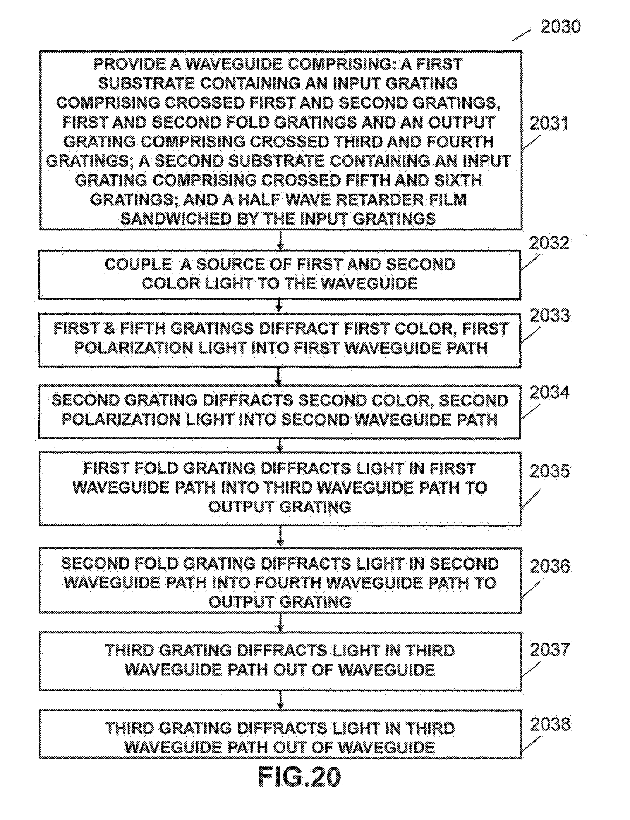
[0089] In some embodiments using gratings recorded in liquid crystal polymer material systems at least one polarization control layer overlapping at least one of the fold gratings, input gratings or output gratings may be provided for the purposes of compensating for polarization rotation in any the gratings, particularly the fold gratings, which the inventors have found may result in polarization rotation. FIG. 10 illustrates one such embodiment in which a waveguide device comprises a waveguide 201 comprising input grating 202, fold grating 203 and output grating 204. In some embodiments, all of the gratings are overlaid by polarization control layers such as the ones reference by 202-204. In some embodiments polarization control layers are applied to the fold gratings only or to any other subset of the gratings. The polarization control layer may comprise an optical retarder film. In some embodiments based on HPDLC materials the birefringence of the gratings may be used to control the polarization properties of the waveguide device. The use the birefringence tensor of the HPDLC grating, K-vectors and grating footprints as design variables opens up the design space for optimizing the angular capability and optical efficiency of the waveguide device.
[0090] In some embodiments the input, output and fold gratings may be recorded in separate layers within a waveguide. For example, in the two-layer design shown in FIG. 11, a waveguide 211 the input grating comprises the separate overlapping grating layers 212,213, the output grating comprising the overlapping layers 214,215 and fold gratings (non-overlapping) 216,217.
[0091] In some embodiments such as the one of FIG. 12 the architecture of FIG. 11 may be implemented using separate waveguides. The waveguides are typically separated by an air gap or a thin layer of low refractive index optical material. In the embodiment 220 shown in FIG. 12, a first waveguide 221 contains the input grating 223, the fold grating 224 and the output grating 225 and a second waveguide 222 contains the input grating 226, the fold grating 227 and the output grating 228. In some embodiments, the first waveguide provides a first input-fold-output grating path and the second waveguide provides a second input-fold-output grating path.
[0092] In the embodiment of FIG. 1 and in the embodiments to be described below at least one of the input, fold and output gratings may be electrically switchable. In many embodiments, it is desirable that all three grating types are passive, that is, non-switching.
[0093] In some embodiments the input grating, fold grating and the output grating are holographic gratings, such as a switchable or non-switchable Bragg Gratings. In some embodiments, the input coupler, the fold grating, and the output grating embodied as SBGs can be Bragg gratings recorded in a holographic polymer dispersed liquid crystal (HPDLC) (e.g., a matrix of liquid crystal droplets), although SBGs may also be recorded in other materials. In one embodiment, SBGs are recorded in a uniform modulation material, such as POLICRYPS or POLIPHEM having a matrix of solid liquid crystals dispersed in a liquid polymer. The SBGs can be switching or non-switching in nature. In its non-switching form an SBG has the advantage over conventional holographic photopolymer materials of being capable of providing high refractive index modulation due to its liquid crystal component. Exemplary uniform modulation liquid crystal-polymer material systems are disclosed in United State Patent Application Publication No.: US2007/0019152 by Caputo et al and PCT Application No.: PCT/EP2005/006950 by Stumpe et al. both of which are incorporated herein by reference in their entireties. Uniform modulation gratings are characterized by high refractive index modulation (and hence high diffraction efficiency) and low scatter. In some embodiments, the input coupler, the fold grating, and the output grating are recorded in a reverse mode HPDLC material. Reverse mode HPDLC differs from conventional HPDLC in that the grating is passive when no electric field is applied and becomes diffractive in the presence of an electric field. The reverse mode HPDLC may be based on any of the recipes and processes disclosed in PCT Application No.: PCT/GB2012/000680, entitled IMPROVEMENTS TO HOLOGRAPHIC POLYMER DISPERSED LIQUID CRYSTAL MATERIALS AND DEVICES. The gratings may be recorded in any of the above material systems but used in a passive (non-switching) mode. The advantage of recording a passive grating in a liquid crystal polymer material is that the final hologram benefits from the high index modulation afforded by the liquid crystal. Higher index modulation translates to high diffraction efficiency and wide angular bandwidth. The fabrication process is identical to that used for switched but with the electrode coating stage being omitted. LC polymer material systems are highly desirable in view of their high index modulation. In some embodiments the gratings are recorded in HPDLC but are not switched.
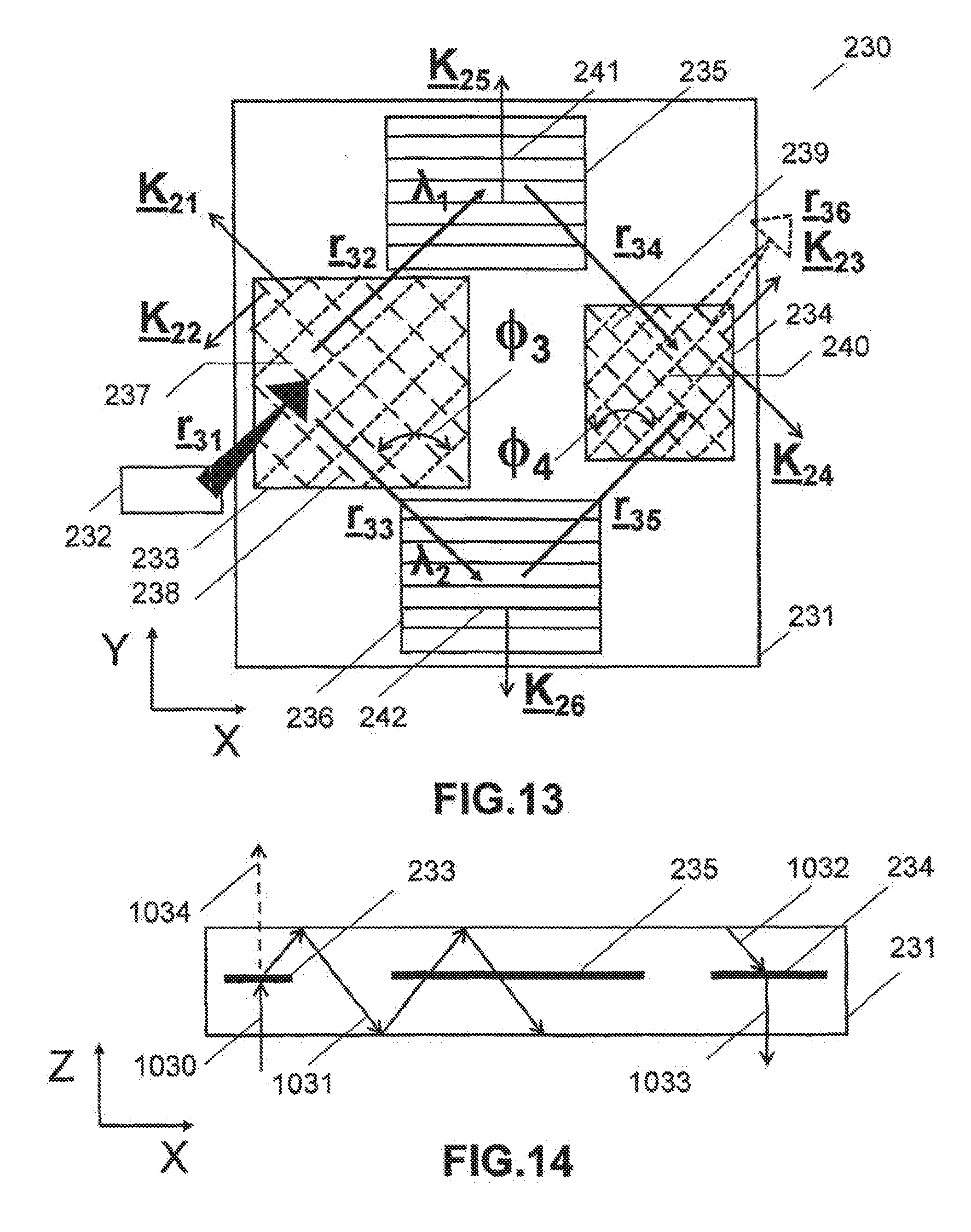
[0094] In some embodiments such as the one illustrated in FIGS. 13-14 the invention provides a means for propagating at least two beams of differing spectral bandwidth through the waveguide. FIG. 13 is a plan view of an embodiment 230 comprising a waveguide 230 of similar architecture to the one of FIG. 1 coupled to the light source 232. The input grating 233 and output grating 234 each combine crossed gratings with peak diffraction efficiency for orthogonal polarizations states, typically S-polarized and P-polarized. In FIG. 1 the input grating is formed from the crossed slant gratings 237,238 having grating vectors K.sub.21,K.sub.22, with the grating fringes being rotated in the waveguide plane (or clocked) at the relative angle and the output grating is formed from the crossed slant gratings 239,240 having grating vectors K.sub.23,K.sub.24, with the grating fringes being rotated in the waveguide plane (or clocked) at the relative angle .PHI..sub.4. The fold gratings 235,236 contain the slant gratings 241,242 having grating vectors K.sub.25K.sub.26. In some embodiments, the angles .PHI..sub.3 and .PHI..sub.4 are each equal to 90 degrees. A first polarization component of the input light from the source with wavelength .lamda..sub.1 incident on the input grating along the direction r.sub.31 is directed by the grating 107 into a TIR path along the direction r.sub.32. A second polarization component with wavelength .lamda..sub.2 is directed by the second grating 108 into a second TIR path along the direction r.sub.33. The light along the paths r.sub.32, r.sub.33 is expanded (in the XY plane of the drawing) by the fold gratings and diffracted into the TIR paths r.sub.34 and r.sub.35 towards the output grating. FIG. 14 shows a cross section view of the waveguide of FIG. 13 showing the input grating 233, output grating 234 and one of the fold gratings 235. The ray path r.sub.31, r.sub.32, r.sub.33 for the light of wavelength is represented by the rays 1030-1032 in FIG. 14 with the output light indicated by 1033 (r.sub.16 in FIG. 13). Since only the first polarization component of the light of wavelength and the second component of the light of wavelength is coupled into the waveguide the embodiment of FIGS. 13-14 will have an optical efficiency not greater than 50%. Light not coupled into the waveguide will propagate through the input grating without substantial deviation as indicated by the ray 1034 in FIG. 14. The embodiment of FIGS. 13-14 would
[0095] In one embodiment 250 there is provided a waveguide for propagating light of more than one color, based on the embodiment of FIGS. 13-14, which includes a means for polarization recovery. As explained above by using crossed input gratings, we ensure that each input light polarization will be correctly aligned for diffraction by one of the crossed gratings. In a color waveguide application, we have at least two input polarizations and at least two colour components. Hence we require two crossed grating layers. The waveguide in the embodiment 250 comprises two bonded substrates, the lower one of which is essentially the waveguide 231 of FIGS. 13-14 and upper one 251 containing an input grating 252 overlaying the input grating of the lower substrate. The upper and lower input gratings sandwich a half wave retarder film 253. The input grating in the upper substrate is formed from the crossed slant gratings 253,254 having grating vectors K.sub.27, K.sub.28, with the grating fringes being rotated in the waveguide plane (or clocked) at the relative angle .PHI..sub.5.
[0096] FIG. 16 shows a cross section view of the embodiment 250 showing the upper substrate 251 and lower substrate 231 containing the input grating 233, output grating 234 and one of the fold gratings 235. The ray path r.sub.31, r.sub.32, r.sub.33 for the light of wavelength .lamda..sub.2, as shown in FIG. 13, which now corresponds to the TIR path between the upper surface of substrate 251 and the lower surface of substrate 231, is represented by the rays 1040-1042 in FIG. 16. Light not diffracted by the input grating 233 propagates upwards as light 1042 and is diffracted by the input grating of the upper substrate The first polarization component of the input light with wavelength .lamda..sub.1 incident on the input grating along the directions (indicated by 1044 in FIG. 16) is directed by the grating 253 into a TIR path along the direction in and a second polarization component with wavelength .lamda..sub.2 is directed by the second grating 254 into a second TIR path along the direction r.sub.38. The TIR paths take place between the upper surface of substrate 251 and the lower surface of substrate 231. The output light from the waveguide is indicated in the case of the light diffracted by the input grating of the lower substrate by 1047 and in the case of the light diffracted by the input grating of the lower substrate by 1948. In summary, the embodiment 250 provides two important benefits. Firstly, it provides separate crosstalk-free waveguide paths for light of different colors. Secondly, it allows utilization of light of any polarization state overcoming the limitation that liquid crystal based gratings such as SBGs are fundamentally polarization sensitive. Only one output grating layer is required since all the waveguide guided light after the input gratings is at the correction polarization for diffraction by the fold and output gratings (P-polarized in the case of SBGs).
[0097] In some embodiments based on the ones illustrated is FIGS. 13-16 the first wavelength corresponds to red light and the second wavelength to blue green light. In some embodiments, the input and output gratings may combine more than two gratings each grating operating on a unique polarization state and a unique spectral bandwidth. In some embodiments, the input and output gratings may combine more than two gratings each grating operating on a unique polarization state, a unique diffraction efficiency angular bandwidth and a unique spectral bandwidth.
[0098] In one embodiment illustrated in the flow diagram of FIG. 17 a method of coupling light of more than one polarization component into a waveguide is provided is provided. Referring to the flow diagram, we see that the said method comprises the following steps.
[0099] At step 2001 provide a waveguide containing an input grating comprising crossed first and second gratings.
[0100] At step 2002 Couple a source of light to the waveguide.
[0101] At step 2003 the first grating diffracts a first polarization state of the light into a first waveguide path.
[0102] At step 2004 simultaneously with step 2004 the first grating diffracts a second polarization state of the light into a second waveguide path.
[0103] In one embodiment illustrated in the flow diagram of FIG. 18 a method 2010 of coupling light of more than one polarization component into a waveguide is provided is provided.
[0104] Referring to the flow diagram, we see that the said method comprises the following steps.
[0105] At step 2011 provide a waveguide containing an input grating comprising crossed first and second gratings; first and second fold gratings; and an output grating comprising crossed third and fourth gratings.
[0106] At step 2012 couple a source of light to the waveguide.
[0107] At step 2013 the first grating diffracts a first polarization state of the light into a first waveguide path.
[0108] At step 2014 simultaneously with step 2004 the first grating diffracts a second polarization state of the light into a second waveguide path.
[0109] At step 2015 the first fold grating diffracts light the first waveguide path into a third waveguide path to the output grating.
[0110] At step 2016 simultaneously with step 2015 the second fold grating diffracts light in the second waveguide path into a fourth waveguide path to the output grating.
[0111] At step 2017 the third grating diffracts light is the third waveguide path out of the waveguide.
[0112] At step 2018 simultaneously with step 2017 the fourth grating diffracts light in the fourth waveguide path out of the waveguide.
[0113] In one embodiment illustrated in the flow diagram of FIG. 19 a method 2020 of coupling light of more than one polarization component and more than one color into a waveguide is provided is provided. Referring to the flow diagram, we see that the said method comprises the following steps.
[0114] At step 2021 provide a waveguide containing an input grating comprising crossed first and second gratings; first and second fold gratings; and an output grating comprising crossed third and fourth gratings.
[0115] At step 2022 couple a source of light of first and second colors to the waveguide.
[0116] At step 2023 the first grating diffracts a first color, first polarization state of the light into a first waveguide path.
[0117] At step 2024 simultaneously with step 2004 the first grating diffracts a second color, second polarization state of the light into a second waveguide path.
[0118] At step 2025 the first fold grating diffracts light the first waveguide path into a third waveguide path to the output grating.
[0119] At step 2026 simultaneously with step 2015 the second fold grating diffracts light in the second waveguide path into a fourth waveguide path to the output grating.
[0120] At step 2027 the third grating diffracts light in the third waveguide path out of the waveguide.
[0121] At step 2028 simultaneously with step 2017 the fourth grating diffracts light in the fourth waveguide path out of the waveguide.
[0122] In one embodiment illustrated in the flow diagram of FIG. 20 a method 2030 of coupling light of more than one polarization component and more than one color into a waveguide is provided is provided. Referring to the flow diagram, we see that the said method comprises the following steps.
[0123] At step 2031 provide a waveguide comprising a first substrate containing an input grating comprising crossed first and second gratings, first and second fold gratings, and an output grating comprising crossed third and fourth gratings; a second substrate containing an input grating comprising crossed fifth and sixth gratings; and a half wave retarder film sandwiched by the input gratings
[0124] At step 2032 couple a source of light of first and second colors to the waveguide.
[0125] At step 2033 the first and fifth gratings diffract a first color, first polarization state of the light into a first waveguide path.
[0126] At step 2034 simultaneously with step 2004 the second and sixth gratings diffract a second color, second polarization state of the light into a second waveguide path.
[0127] At step 2035 the first fold grating diffracts light the first waveguide path into a third waveguide path to the output grating.
[0128] At step 2036 simultaneously with step 2013 the second fold grating diffracts light in the second waveguide path into a fourth waveguide path to the output grating.
[0129] At step 2037 the third grating diffracts light in the third waveguide path out of the waveguide.
[0130] At step 2038 simultaneously with step 2017 the fourth grating diffracts light in the fourth waveguide path out of the waveguide.
[0131] In display applications of the invention the apparatus will normally further comprise an input image node (IIN) optically coupled to the waveguide. Typically, the IIN integrates a microdisplay panel, light source and optical components needed to illuminate the display panel, separate the reflected light and collimate it into the required FOV. The invention does not assume any particular microdisplay technology. In some embodiments the microdisplay panel be a liquid crystal device or a MEMS device. In some embodiments the microdisplay may be based on Organic Light Emitting Diode (OLED) technology. Such emissive devices would not require a separate light source and would therefore offer the benefits of a smaller form factor. In some embodiments the IIN may be based on a scanned modulated laser. The IIN projects the image displayed on the microdisplay panel such that each display pixel is converted into a unique angular direction within the substrate waveguide according to some embodiments. The collimation optics contained in the IIN may comprise lens and mirrors which is some embodiments may be diffractive lenses and mirrors. In some embodiments the IIN may be based on the embodiments and teachings disclosed in U.S. patent application Ser. No. 13/869,866 entitled HOLOGRAPHIC WIDE ANGLE DISPLAY, and U.S. patent application Ser. No. 13/844,456 entitled TRANSPARENT WAVEGUIDE DISPLAY. In some embodiments the IIN contains beamsplitter for directing light onto the microdisplay and transmitting the reflected light towards the waveguide. In one embodiment the beamsplitter is a grating recorded in HPDLC and uses the intrinsic polarization selectivity of such gratings to separate the light illuminating the display and the image modulated light reflected off the display. In some embodiments the beam splitter is a polarizing beam splitter cube. In some embodiment the IIN incorporates a despeckler. Advantageously, the despeckler is holographic waveguide device based on the embodiments and teachings of U.S. Pat. No. 8,565,560 entitled LASER ILLUMINATION DEVICE. The light source can be a laser or LED and can include one or more lenses for modifying the illumination beam angular characteristics. The image source can be a micro-display or laser based display. LED will provide better uniformity than laser. If laser illumination is used there is a risk of illumination banding occurring at the waveguide output. In some embodiments laser illumination banding in waveguides can be overcome using the techniques and teachings disclosed in U.S. Provisional Patent Application No. 62/071,277 entitled METHOD AND APPARATUS FOR GENERATING INPUT IMAGES FOR HOLOGRAPHIC WAVEGUIDE DISPLAYS. In some embodiments, the light from the light source 101 is polarized. In one or more embodiments, the image source is a liquid crystal display (LCD) micro display or liquid crystal on silicon (LCoS) micro display.
[0132] In some embodiments, the fold grating angular bandwidth can be enhanced by designing the grating prescription to facilitate dual interaction of the guided light with the grating. Exemplary embodiments of dual interaction fold gratings are disclosed in U.S. patent application Ser. No. 14/620,969 entitled WAVEGUIDE GRATING DEVICE.
[0133] In some embodiments, at least one of the input, fold or output gratings may be based on surface relief structures.
[0134] In some embodiments, at least one of the input, fold or output gratings may combine two or more angular diffraction prescriptions to expand the angular bandwidth. Similarly, in some embodiments at least one of the input, fold or output gratings may comb one two or more spectral diffraction prescriptions to expand the spectral bandwidth. For example, a color multiplexed grating may be used to diffract two or more of the primary colors.
[0135] In some embodiments, the cell substrates may be fabricated from glass. An exemplary glass substrate is standard Corning Willow glass substrate (index 1.51) which is available in thicknesses down to 50 microns. In other embodiments, the cell substrates may be optical plastics.
[0136] In some embodiments, the grating layer may be broken up into separate layers. For example, in some embodiments, a first layer includes the fold grating while a second layer includes the output grating. In some embodiments, a third layer can include the input grating. The number of layers may then be laminated together into a single waveguide substrate. In some embodiments, the grating layer is comprised of a number of pieces including the input coupler, the fold grating and the output grating (or portions thereof) that are laminated together to form a single substrate waveguide. The pieces may be separated by optical glue or other transparent material of refractive index matching that of the pieces. In another embodiment, the grating layer may be formed via a cell making process by creating cells of the desired grating thickness and vacuum filling each cell with SBG material for each of the input coupler, the fold grating and the output grating. In one embodiment, the cell is formed by positioning multiple plates of glass with gaps between the plates of glass that define the desired grating thickness for the input coupler, the fold grating and the output grating. In one embodiment, one cell may be made with multiple apertures such that the separate apertures are filled with different pockets of SBG material. Any intervening spaces may then be separated by a separating material (e.g., glue, oil, etc.) to define separate areas. In one embodiment the SBG material may be spin-coated onto a substrate and then covered by a second substrate ate curing of the material.
[0137] By using the fold grating, the waveguide device advantageously requires fewer layers than previous systems and methods of displaying information according to some embodiments. In addition, by using fold grating, light can travel by total internal refection within the waveguide in a single rectangular prism defined by the waveguide outer surfaces while achieving dual pupil expansion.
[0138] In some embodiment, the input grating, the fold grating and the output grating can be created by interfering two waves of light at an angle within the substrate to create a holographic wave front, thereby creating light and dark fringes that are set in the waveguide substrate 101 at a desired angle. In some embodiments the grating in a given layer is recorded in stepwise fashion by scanning or stepping the recording laser beams across the grating area. In some embodiments the gratings are recorded using mastering and contact copying process currently used in the holographic printing industry.
[0139] In some embodiments red, green and blue diffracting grating layers based on the principles discussed above may be provided for color unpolarized illumination. In some embodiments a color waveguide according to the principles of the invention may use just one grating layer in each monochromatic waveguide. In some embodiments waveguides based on the principles discussed above operate in the infrared band.
[0140] In some embodiments directed at displays, the fold grating may be oriented in a diagonal direction. The fold grating is configured to provide pupil expansion in a first direction and to direct the light to the output grating via total internal reflection inside the waveguide in some embodiments. In one embodiment, a longitudinal edge of each fold grating is oblique to the axis of alignment of the input coupler such that each fold grating is set on a diagonal with respect to the direction of propagation of the display light. The fold grating is angled such that light from the input coupler is redirected to the output grating. In one example, the fold grating is set at a forty-five-degree angle relative to the direction that the display image is released from the input coupler. This feature causes the display image propagating down the fold grating to be turned into the output grating. For example, in one embodiment, the fold grating causes the image to be turned 90 degrees into the output grating. In this manner, a single waveguide provides dual axis pupil expansion in both the horizontal and vertical directions. In one embodiment, each of the fold grating may have a partially diffractive structure. The output grating is configured to provide pupil expansion in a second direction different than the first direction and to cause the light to exit the waveguide from the first surface or the second surface. The output grating receives the image light from the fold grating via total internal reflection and provides pupil expansion in a second direction. In some embodiments, the output grating consists of multiple layers of substrate, thereby comprising multiple layers of output gratings. Accordingly, there is no requirement for gratings to be in one plane within the waveguide, and gratings may be stacked on top of each other (e.g., cells of gratings stacked on top of each other).
[0141] In some embodiments, a quarter wave plate disposed on a glass-air interface of the wave guide rotates polarization of a light ray to maintain efficient coupling with the gratings. For example, in one embodiment, the quarter wave plate is a coating that is applied to substrate waveguide. The quarter wave plate provides light wave polarization management. In a display application such polarization management may help light rays retain alignment with the intended viewing axis by compensating for skew waves in the waveguide. The quartet wave plate may be provided as multi-layer coating.
[0142] In one embodiment of the invention directed at displays shown in FIG. 7 a waveguide display according to the principles of the invention is combined with an eye tracker. In one preferred embodiment the eye tracker is a waveguide device overlaying the display waveguide and is based on the embodiments and teachings of PCT/GB2014/00019 entitled HOLOGRAPHIC WAVEGUIDE EYE TRACKER, PCT/GB2015/000274 entitled HOLOGRAPHIC WAVEGUIDE OPTICALTRACKER, and PCT Application No.: GB2013/000210 entitled APPARATUS FOR EYE TRACKING.
[0143] In some embodiments of the invention directed at displays a waveguide display according to the principles of the invention further comprises a dynamic focusing element. The dynamic focusing element may be based on the embodiments and teachings of U.S. Provisional Patent Application No.: 62/176,572 entitled ELECTRICALLY FOCUS TUNABLE LENS. In some embodiment a waveguide display according to the principles of the invention further comprising a dynamic focusing element and an eye tracker may provide a light field display based on the embodiments and teachings disclosed in U.S. Provisional Patent Application No.: 62/125,089 entitled HOLOGRAPHIC WAVEGUIDE LIGHT FIELD DISPLAYS.
[0144] In some embodiments of the invention directed at displays a waveguide according to the principles of the invention may be based on some of the embodiments of U.S. patent application Ser. No. 13/869,866 entitled HOLOGRAPHIC WIDE ANGLE DISPLAY, and U.S. patent application Ser. No. 13/844,456 entitled TRANSPARENT WAVEGUIDE DISPLAY. In some embodiments a waveguide apparatus according to the principles of the invention may be integrated within a window, for example a windscreen-integrated HUD for road vehicle applications. In some embodiments a window-integrated display may be based on the embodiments and teachings disclosed in U.S. Provisional Patent Application No.: PCT Application No.: PCT/GB2016/000005 entitled ENVIRONMENTALLY ISOLATED WAVEGUIDE DISPLAY. In some embodiments a waveguide apparatus may include gradient index (GRIN) wave-guiding components for relaying image content between the IIN and the waveguide. Exemplary embodiments are disclosed in PCT Application No.: PCT/GB2016/000005 entitled ENVIRONMENTALLY ISOLATED WAVEGUIDE DISPLAY. In some embodiments the waveguide apparatus may incorporate a light pipe for providing beam expansion in one direction based on the embodiments disclosed in U.S. Provisional Patent Application No.: 62/177,494 entitled WAVEGUIDE DEVICE INCORPORATING A LIGHT PIPE.
[0145] The embodiments of the invention may be used in wide range of display applications including HMDs for AR and VR, helmet mounted displays, projection displays, heads up displays (HUDs), Heads Down Displays, (HDDs), autostereoscopic displays and other 3D displays. Some of the embodiments and teachings of this disclosure may be applied in waveguide sensors such as, for example, eye trackers, fingerprint scanners and LIDAR systems.
[0146] It should be emphasized that the drawings are exemplary and that the dimensions have been exaggerated. For example, thicknesses of the SBG layers have been greatly exaggerated. Optical devices based on any of the above-described embodiments may be implemented using plastic substrates using the materials and processes disclosed in PCT Application No.: PCT/GB2012/000680, entitled IMPROVEMENTS TO HOLOGRAPHIC POLYMER DISPERSED LIQUID CRYSTAL MATERIALS AND DEVICES. In some embodiments the dual expansion waveguide display may be curved.
[0147] The construction and arrangement of the systems and methods as shown in the various exemplary embodiments are illustrative only. Although only a few embodiments have been described in detail in this disclosure, many modifications are possible (for example, variations in sizes, dimensions, structures, shapes-and proportions of the various elements, values of parameters, mounting arrangements, use of materials, colors, orientations, etc.). For example, the position of elements may be reversed or otherwise varied and the nature or number of discrete elements or positions may be altered or varied. Accordingly, all such modifications are intended to be included within the scope of the present disclosure. The order or sequence of any process or method steps may be varied or re-sequenced according to alternative embodiments. Other substitutions, modifications, changes, and omissions may be made in the design, operating conditions and arrangement of the exemplary embodiments without departing from the scope of the present disclosure.
* * * * *
D00000
D00001
D00002
D00003
D00004
D00005
D00006
D00007
D00008
D00009
D00010
D00011
P00999
XML
uspto.report is an independent third-party trademark research tool that is not affiliated, endorsed, or sponsored by the United States Patent and Trademark Office (USPTO) or any other governmental organization. The information provided by uspto.report is based on publicly available data at the time of writing and is intended for informational purposes only.
While we strive to provide accurate and up-to-date information, we do not guarantee the accuracy, completeness, reliability, or suitability of the information displayed on this site. The use of this site is at your own risk. Any reliance you place on such information is therefore strictly at your own risk.
All official trademark data, including owner information, should be verified by visiting the official USPTO website at www.uspto.gov. This site is not intended to replace professional legal advice and should not be used as a substitute for consulting with a legal professional who is knowledgeable about trademark law.