Waveguide Device with Uniform Output Illumination
Waldern; Jonathan David ; et al.
U.S. patent application number 16/465834 was filed with the patent office on 2020-01-23 for waveguide device with uniform output illumination. This patent application is currently assigned to Digilens Inc.. The applicant listed for this patent is Digilens Inc.. Invention is credited to Alastair John Grant, Milan Momcilo Popovich, Jonathan David Waldern.
| Application Number | 20200026074 16/465834 |
| Document ID | / |
| Family ID | 62241961 |
| Filed Date | 2020-01-23 |


View All Diagrams
| United States Patent Application | 20200026074 |
| Kind Code | A1 |
| Waldern; Jonathan David ; et al. | January 23, 2020 |
Waveguide Device with Uniform Output Illumination
Abstract
Various embodiments of waveguide devices are described. A debanding optic may be incorporated into waveguide devices, which may help supply uniform output illumination. Accordingly, various waveguide devices are able to output a substantially flat illumination profile eliminating or mitigating banding effects.
| Inventors: | Waldern; Jonathan David; (Los Altos Hills, CA) ; Grant; Alastair John; (San Jose, CA) ; Popovich; Milan Momcilo; (Leicester, GB) | ||||||||||
| Applicant: |
|
||||||||||
|---|---|---|---|---|---|---|---|---|---|---|---|
| Assignee: | Digilens Inc. Sunnyvale CA |
||||||||||
| Family ID: | 62241961 | ||||||||||
| Appl. No.: | 16/465834 | ||||||||||
| Filed: | January 26, 2018 | ||||||||||
| PCT Filed: | January 26, 2018 | ||||||||||
| PCT NO: | PCT/US2018/015553 | ||||||||||
| 371 Date: | May 31, 2019 |
Related U.S. Patent Documents
| Application Number | Filing Date | Patent Number | ||
|---|---|---|---|---|
| 62497781 | Dec 2, 2016 | |||
| 62499423 | Jan 26, 2017 | |||
| Current U.S. Class: | 1/1 |
| Current CPC Class: | G02B 27/0093 20130101; G02B 6/0061 20130101; G02B 6/0023 20130101; G02B 27/0081 20130101; G02B 2027/0116 20130101; G02B 2027/0174 20130101; G02B 2027/0114 20130101; G02B 6/0035 20130101; G02B 6/0076 20130101; G02B 27/0103 20130101; G02B 6/0016 20130101; G02B 27/0101 20130101; G02B 27/0172 20130101 |
| International Class: | G02B 27/01 20060101 G02B027/01; F21V 8/00 20060101 F21V008/00; G02B 27/00 20060101 G02B027/00 |
Claims
1. A waveguide device comprising: at least one optical substrate; at least one light source; at least one light coupler capable of coupling incident light from the light source with an angular bandwidth into a total internal reflection (TIR) within the at least one optical substrate such that a unique TIR angle is defined by each light incidence angle as determined at the input grating; at least one light extractor for extracting the light from the optical substrate; and a debanding optic capable of mitigating banding effects of an illuminated pupil, such that the extracted light is a substantially flat illumination profile having mitigated banding.
2. The waveguide device of claim 1, wherein the extracted light has a spatial non-uniformity less than one of either 10% or 20%.
3. (canceled)
4. The waveguide device of claim 1, wherein the debanding optic is an effective input aperture such that when the optical substrate has a thickness D, the input aperture is configured to provide a TIR angle U in the optical substrate, and the angle U is calculated by 2D tan (U).
5. The waveguide device of claim 4, wherein the debanding optic provides spatial variation of the light along the TIR path of at least one of diffraction efficiency, optical transmission, polarization or birefringence.
6. The waveguide device of claim 1, wherein the debanding optic is at least one grating selected from at least one input grating and at least one output grating, and wherein the selected at least one grating is a configuration selected from the group of: multiple gratings, such that each grating provides a small pupil shift to mitigate banding; a stacked switchable grating that turns on when a voltage is applied, shifting pupil to mitigate banding effects; an array of switchable grating elements that can turn on a specific element when a voltage is applied, shifting pupil to mitigate banding effects; an array of switchable grating elements that can turn on a specific element when a voltage is applied, shifting pupil to mitigate banding effects wherein the selected at least one grating has a plurality of rolled K-vectors; a plurality of passive grating layers configured to shift pupil to mitigate banding effects; one or more index layers disposed within the optical substrate such that the one or more index layers influences the light ray paths within the optical substrate as a function of at least one of ray angle or ray position, shifting pupil to mitigate banding effects; and one or more index layers disposed within the optical substrate such that the one or more index layers influences the light ray paths within the optical substrate as a function of at least one of ray angle or ray position, shifting pupil to mitigate banding effects, wherein at least one index layer of the one or more index layers is a gradient index (GRIN) medium.
7. (canceled)
8. (canceled)
9. (canceled)
10. (canceled)
11. (canceled)
12. (canceled)
13. The waveguide device of claim 1 further comprising at least one reflecting surface on at least a part of an edge of the optical substrate, and wherein the debanding optic is one or more index layers disposed adjacent to the at least one reflecting surface such that the one or more index layers are configured to shift pupil to mitigate banding effects.
14. The waveguide device of claim 1, wherein the debanding optic is selected from the group of: one or more index layers disposed within the optical substrate such that the one or more index layers are configured to shift pupil to mitigate banding effects; an input grating having a leading edge able to couple the incident light such that a unique displacement of a ray bundle of the light relative to the leading edge of the input grating is provided by the input grating for any given incident light direction, shifting pupil to mitigate banding effects; an input grating configured to have a variation of diffraction efficiencies such that a plurality of collimated incident ray paths of the incident light is diffracted into different TIR ray paths, as determined by a ray path input angle, such that a projected pupil is capable of forming at a unique location within the optical substrate for each of the plurality of collimated incident ray paths to mitigate banding effects; an input grating configured to have a variation of diffraction efficiencies such that a plurality of collimated incident ray paths of the incident light is diffracted into different TIR ray paths, as determined by a ray path input angle, such that a projected pupil is capable of forming at a unique location within the optical substrate for each of the plurality of collimated incident ray paths to mitigate banding effects, wherein the variation of diffraction efficiencies varies along a principal waveguide direction; and an input grating configured to have a variation of diffraction efficiencies such that a plurality of collimated incident ray paths of the incident light is diffracted into different TIR ray paths, as determined by a ray path input angle, such that a projected pupil is capable of forming at a unique location within the optical substrate for each of the plurality of collimated incident ray paths to mitigate banding effects, wherein the variation of diffraction efficiencies varies in two dimensions over the aperture of the input grating.
15. (canceled)
16. (canceled)
17. (canceled)
18. (canceled)
19. The waveguide device of claim 1, wherein the debanding optic is selected from the group of: a partially reflecting layer disposed within the optical substrate such that the partially reflecting layer separates incident light into transmitted and reflected light, shifting pupil to mitigate banding effects; a polarization modifying layer disposed within the optical substrate such that the polarization modifying layer separates incident light into transmitted and reflected light, shifting pupil to mitigate banding effects; a plurality of refractive index layers that provide spatial variation along each TIR path of at least one of diffraction efficiency, optical transmission, polarization and birefringence to influence ray paths within a waveguide substrate as a function of at least one of ray angle or ray position within the substrate, resulting in shift of pupil to mitigate banding effects; a plurality of refractive index layers that provide spatial variation along each TIR path of at least one of diffraction efficiency, optical transmission, polarization and birefringence to influence ray paths within a waveguide substrate as a function of at least one of ray angle or ray position within the substrate, resulting in shift of pupil to mitigate banding effects, wherein the plurality of refractive index layers incorporates adhesives of different indices; and a plurality of refractive index layers that provide spatial variation along each TIR path of at least one of diffraction efficiency, optical transmission, polarization and birefringence to influence ray paths within a waveguide substrate as a function of at least one of ray angle or ray position within the substrate, resulting in shift of pupil to mitigate banding effects, wherein the plurality of refractive index layers incorporates layers selected from the group consisting of alignment layers, isotropic refractive layers, GRIN structures, antireflection layers, partially reflecting layer, and birefringent stretched polymer layers.
20. (canceled)
21. The waveguide device of claim 1, wherein the debanding optic is selected from the group of: at least one grating selected from at least one input grating and at least one output grating, and wherein the selected at least one grating is configured to provide at least two separate waveguide paths which cancel non-uniformity of light of the extracted light for any incidence light angle, mitigating banding effects, at least one grating selected from at least one input grating and at least one output grating, and wherein the selected at least one grating is configured to provide at least two separate waveguide paths which cancel non-uniformity of light of the extracted light for any incidence light angle, mitigating banding effects, wherein the selected grating has crossed slant gratings used in conjunction with at least one fold grating exit pupil expander; an optical component within a microdisplay that provides variable effective numerical apertures (NA) capable of being spatially varied along at least one direction to shift pupil shift to mitigate banding effects; a plurality of grating layers within at least one grating of either at least one input grating or at least one output grating such that the plurality of grating layers is configured to smear out any fixed pattern noise resulting in shift of pupil to mitigate banding effects; and an input grating configured as an array of selectively switchable elements such that configuring the input grating as a switching grating array provides pupil switching in vertical and horizontal directions to shift pupil to mitigate banding effects.
22. (canceled)
23. (canceled)
24. (canceled)
25. (canceled)
26. (canceled)
27. (canceled)
28. (canceled)
29. The waveguide device of claim 1, wherein the debanding optic is selected from the group of: a microdisplay projecting spatially varied numerical apertures that shift pupil to mitigate banding effects; a tilted microdisplay configured to project a tilted, rectangular exit pupil such that the cross section of the exit pupil varies with a field angle, such that banding effects are mitigated; a tilted microdisplay configured to angle light rays to form various projected pupils at different positions along the optical substrate for each angle of incident light, such that banding effects are mitigated along one expansion axis; a light-absorbing film adjacent to the edges of the optical substrate such that portions of the incident light, that would otherwise give rise to banding, are removed, mitigating banding effects; and an input grating configured such that the light has a unique displacement relative to an edge of the input grating at any given incident light direction to shift pupil, eliminating or mitigating a banding effect.
30. (canceled)
31. (canceled)
32. The waveguide device of claim 1, wherein the optical substrate has a thickness D, and wherein the debanding optic is selected from the group of: a prism coupled to the optical substrate, such that a linear relationship between the angles of an exit pupil from the light source and the TIR angles in the optical substrate result in no gaps between successive light extractions along the TIR ray path, which occurs when the TIR path angle is U as defined by 2D tan (U); a first light-absorbing film disposed adjacent to the edges an input substrate containing an input grating and disposed adjacent to the optical substrate, and a second light-absorbing film disposed adjacent to the edges a second substrate, attached adjacent to the optical substrate opposite the input substrate, such that incident light results in no gaps between successive light extractions along the TIR ray path, which occurs when the TIR path angle is U as defined by 2D tan (U); and a first light-absorbing film disposed adjacent to the edges an input substrate containing an input grating and disposed adjacent to the optical substrate, and a second light-absorbing film disposed adjacent to the edges a second substrate, attached adjacent to the optical substrate opposite the input substrate, such that incident light results in no gaps between successive light extractions along the TIR ray path, which occurs when the TIR path angle is U as defined by 2D tan (U), wherein the thickness of the optical substrate is 3.4 mm, the thickness of the second is substrate 0.5 mm, and the input substrate contains two 0.5 mm thick glass substrates sandwiching the input grating.
33. (canceled)
34. (canceled)
35. (canceled)
36. (canceled)
37. The waveguide device of claim 1, wherein the device is integrated into a display selected from the group of head mounted display (HMD) and a head up display (HUD).
38. The waveguide device of claim 37, wherein at least one of the following: a human eye is positioned with an exit pupil of the display; and the device incorporates an eye tracker.
39. (canceled)
40. The waveguide device of claim 1 further comprising an input image generator that further comprises the light source, a microdisplay panel, and optics for collimating the light.
41. The waveguide device of claim 1, wherein the light source is selected from the group of: at least one laser, and at least one light emitting diode (LED).
42. (canceled)
43. The waveguide device of claim 1, wherein the light coupler is selected from the group of an input grating; and a prism.
44. (canceled)
45. The waveguide device of claim 1, wherein the light extractor is an input grating.
46. A color waveguide device comprising: at least two optical substrates stacked upon each other; at least one light source; at least one light coupler capable of coupling incident light from the light source with an angular bandwidth into a total internal reflection (TIR) within the at least one optical substrate such that a unique TIR angle is defined by each light incidence angle as determined at the input grating; at least one light extractor for extracting the light from the optical substrate; and at least two input stops, each input stop is within a different optical substrate, each in a different plane, wherein each input stop includes an outer dichroic portion to shift pupil and mitigate color banding.
47. The color waveguide device of claim 46, wherein each input stop also includes an inner phase compensation coating to compensate for a phase shift.
48. The color waveguide device of claim 47, wherein the compensation coating includes SiO.sub.2.
49. A method to mitigate banding in an output illumination of a waveguide device, comprising: producing incident light from a light source; passing the incident light through a light coupler to couple the incident light into an optical substrate such that the coupled light undergoes total internal reflection (TIR) within the optical substrate; and extracting the TIR light from the optical substrate via a light extractor to produce the output illumination; wherein the light passes through a debanding optic of the waveguide device such that the debanding optic mitigates a banding effect of the output illumination.
50. The method of claim 49, wherein the output illumination has a spatial non-uniformity less than one of either 10% or 20%.
51. (canceled)
52. The method of claim 49, wherein the debanding optic is selected from the group of: an effective input aperture such that when the optical substrate has a thickness D, the input aperture is configured to provide a TIR angle U in the optical substrate, and the angle U is calculated by 2D tan (U); an effective input aperture such that when the optical substrate has a thickness D, the input aperture is configured to provide a TIR angle U in the optical substrate, and the angle U is calculated by 2D tan (U), wherein the debanding optic provides spatial variation of the light along the TIR path of at least one of diffraction efficiency, optical transmission, polarization or birefringence; at least one grating selected from at least one input grating and at least one output grating, and wherein the selected at least one grating is configured to have multiple gratings, such that each grating provides a small pupil shift to mitigate banding; at least one grating selected from at least one input grating and at least one output grating, and wherein the selected at least one grating is configured as a stacked switchable grating that turns on when a voltage is applied, shifting pupil to mitigate banding effects; at least one grating selected from at least one input grating and at least one output grating, and wherein the selected at least one grating is configured as an array of switchable grating elements that can turn on a specific element when a voltage is applied, shifting pupil to mitigate banding effects; at least one grating selected from at least one input grating and at least one output grating, and wherein the selected at least one grating is configured as an array of switchable grating elements that can turn on a specific element when a voltage is applied, shifting pupil to mitigate banding effects, wherein the selected at least one grating has a plurality of rolled K-vectors; at least one grating selected from at least one input grating and at least one output grating, and wherein the selected at least one grating is configured to be a plurality of passive grating layers configured to shift pupil to mitigate banding effects; one or more index layers disposed within the optical substrate such that the one or more index layers influences the light ray paths within the optical substrate as a function of at least one of ray angle or ray position, shifting pupil to mitigate banding effects; and one or more index layers disposed within the optical substrate such that the one or more index layers influences the light ray paths within the optical substrate as a function of at least one of ray angle or ray position, shifting pupil to mitigate banding effects, wherein at least one index layer of the one or more index layers is a gradient index (GRIN) medium.
53. (canceled)
54. (canceled)
55. (canceled)
56. (canceled)
57. (canceled)
58. (canceled)
59. (canceled)
60. (canceled)
61. The method of claim 49, wherein the waveguide device further comprises at least one reflecting surface on at least a part of an edge of the optical substrate, and wherein the debanding optic is one or more index layers disposed adjacent to the at least one reflecting surface such that the one or more index layers are configured to shift pupil to mitigate banding effects.
62. The method of claim 49, wherein the debanding optic is selected from the group of: one or more index layers disposed within the optical substrate such that the one or more index layers are configured to shift pupil to mitigate banding effects; an input grating having a leading edge able to couple the incident light such that a unique displacement of a ray bundle of the light relative to the leading edge of the input grating is provided by the input grating for any given incident light direction, shifting pupil to mitigate banding effects; an input grating configured to have a variation of diffraction efficiencies such that a plurality of collimated incident ray paths of the incident light is diffracted into different TIR ray paths, as determined by a ray path input angle, such that a projected pupil is capable of forming at a unique location within the optical substrate for each of the plurality of collimated incident ray paths to mitigate banding effects; an input grating configured to have a variation of diffraction efficiencies such that a plurality of collimated incident ray paths of the incident light is diffracted into different TIR ray paths, as determined by a ray path input angle, such that a projected pupil is capable of forming at a unique location within the optical substrate for each of the plurality of collimated incident ray paths to mitigate banding effects, wherein the variation of diffraction efficiencies varies along a principal waveguide direction; an input grating configured to have a variation of diffraction efficiencies such that a plurality of collimated incident ray paths of the incident light is diffracted into different TIR ray paths, as determined by a ray path input angle, such that a projected pupil is capable of forming at a unique location within the optical substrate for each of the plurality of collimated incident ray paths to mitigate banding effects wherein the variation of diffraction efficiencies varies in two dimensions over the aperture of the input grating; a partially reflecting layer disposed within the optical substrate such that the partially reflecting layer separates incident light into transmitted and reflected light, shifting pupil to mitigate banding effects; a polarization modifying layer disposed within the optical substrate such that the polarization modifying layer separates incident light into transmitted and reflected light, shifting pupil to mitigate banding effects; at least one grating selected from at least one input grating and at least one output grating, and wherein the selected at least one grating is configured to provide at least two separate waveguide paths which cancel non-uniformity of light of the extracted light for any incidence light angle, mitigating banding effects; at least one grating selected from at least one input grating and at least one output grating, and wherein the selected at least one grating is configured to provide at least two separate waveguide paths which cancel non-uniformity of light of the extracted light for any incidence light angle, mitigating banding effects, wherein the selected grating has crossed slant gratings used in conjunction with at least one fold grating exit pupil expander; an optical component within a microdisplay that provides variable effective numerical apertures (NA) capable of being spatially varied along at least one direction to shift pupil shift to mitigate banding effects; a plurality of grating layers within at least one grating of either at least one input grating or at least one output grating such that the plurality of grating layers is configured to smear out any fixed pattern noise resulting in shift of pupil to mitigate banding effects; an input grating configured as an array of selectively switchable elements such that configuring the input grating as a switching grating array provides pupil switching in vertical and horizontal directions to shift pupil to mitigate banding effects; a plurality of refractive index layers that provide spatial variation along each TIR path of at least one of diffraction efficiency, optical transmission, polarization and birefringence to influence ray paths within a waveguide substrate as a function of at least one of ray angle or ray position within the substrate, resulting in shift of pupil to mitigate banding effects; a plurality of refractive index layers that provide spatial variation along each TIR path of at least one of diffraction efficiency, optical transmission, polarization and birefringence to influence ray paths within a waveguide substrate as a function of at least one of ray angle or ray position within the substrate, resulting in shift of pupil to mitigate banding effects, wherein the plurality of refractive index layers incorporates adhesives of different indices; a plurality of refractive index layers that provide spatial variation along each TIR path of at least one of diffraction efficiency, optical transmission, polarization and birefringence to influence ray paths within a waveguide substrate as a function of at least one of ray angle or ray position within the substrate, resulting in shift of pupil to mitigate banding effects, wherein the plurality of refractive index layers incorporate layers selected from the group consisting of alignment layers, isotropic refractive layers, GRIN structures, antireflection layers, partially reflecting layer, and birefringent stretched polymer layers; a microdisplay projecting spatially varied numerical apertures that shift pupil to mitigate banding effects; a tilted microdisplay configured to project a tilted, rectangular exit pupil such that the cross section of the exit pupil varies with a field angle, such that banding effects are mitigated; a tilted microdisplay configured to angle light rays to form various projected pupils at different positions along the optical substrate for each angle of incident light, such that banding effects are mitigated along one expansion axis; a light-absorbing film adjacent to the edges of the optical substrate such that portions of the incident light, that would otherwise give rise to banding, are removed, mitigating banding effects; an input grating configured such that the light has a unique displacement relative to an edge of the input grating at any given incident light direction to shift pupil, eliminating or mitigating a banding effect
63. (canceled)
64. (canceled)
65. (canceled)
66. (canceled)
67. (canceled)
68. (canceled)
69. (canceled)
70. (canceled)
71. (canceled)
72. (canceled)
73. (canceled)
74. (canceled)
75. (canceled)
76. (canceled)
77. (canceled)
78. (canceled)
79. (canceled)
80. The method of claim 49, wherein the optical substrate has a configuration selected from the group of: a thickness D, and wherein the debanding optic is a prism coupled to the optical substrate, such that a linear relationship between the angles of an exit pupil from the light source and the TIR angles in the optical substrate result in no gaps between successive light extractions along the TIR ray path, which occurs when the TIR path angle is U as defined by 2D tan (U); a thickness D, and wherein the debanding optic is a first light-absorbing film disposed adjacent to the edges of an input substrate containing an input prating and disposed adjacent to the optical substrate, and a second light-absorbing film disposed adjacent to the edges a second substrate, attached adjacent to the optical substrate opposite the input substrate, such that incident light results in no gaps between successive light extractions along the TIR ray path, which occurs when the TIR path angle is U as defined by 2D tan (U); and a thickness D, and wherein the debanding optic is a first light-absorbing film disposed adjacent to the edges of an input substrate containing an input grating and disposed adjacent to the optical substrate, and a second light-absorbing film disposed adjacent to the edges a second substrate, attached adjacent to the optical substrate opposite the input substrate, such that incident light results in no gaps between successive light extractions along the TIR ray path, which occurs when the TIR path angle is U as defined by 2D tan (U), wherein the thickness of the optical substrate is 3.4 mm, the thickness of the second is substrate 0.5 mm, and the input substrate contains two 0.5 mm thick glass substrates sandwiching the input grating.
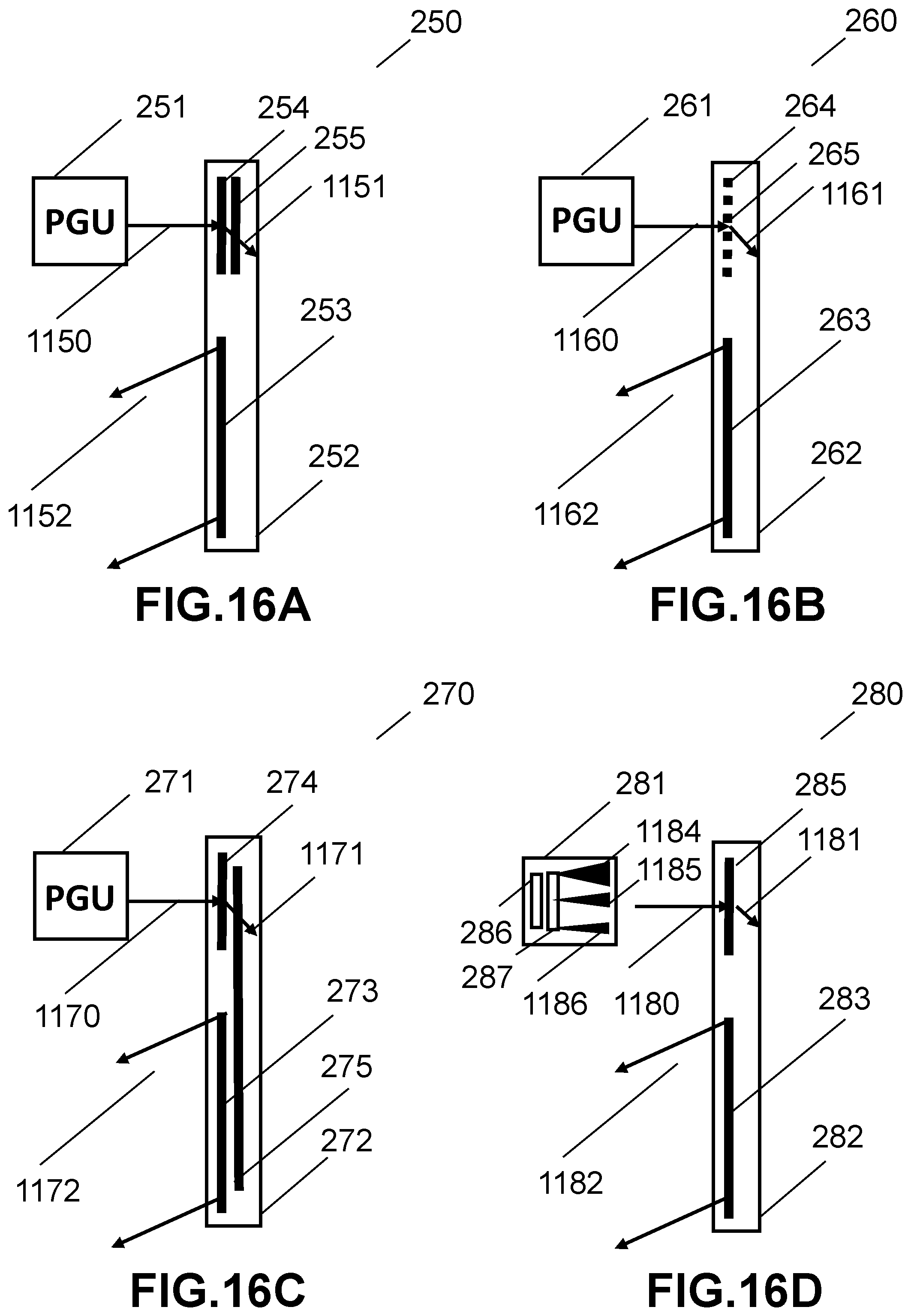
81. (canceled)
82. (canceled)
83. (canceled)
84. (canceled)
85. The method of claim 49, wherein the method is performed by a display selected from the group of head mounted display (HMD) and a head up display (HUD).
86. The method of claim 85, wherein at least one of: a human eye is positioned with an exit pupil of the display and the display incorporates an eye tracker.
87. (canceled)
88. The method of claim 49, wherein the waveguide device further comprises an input image generator that further comprises the light source, a microdisplay panel, and optics for collimating the light.
89. The method of claim 49, wherein the light source is selected from the group of: at least one laser; and at least one light emitting diode (LED).
90. (canceled)
91. The method of claim 49, wherein the light coupler is selected from one of: an input grating; and a prism.
92. (canceled)
93. The method of claim 49, wherein the light extractor is an input grating.
Description
FIELD OF THE INVENTION
[0001] The present disclosure relates to waveguide devices and more particularly to waveguides having uniform output illumination.
BACKGROUND OF THE INVENTION
[0002] Waveguide optics are currently being considered for a range of display and sensor applications for which the ability of waveguide devices to integrate multiple optical functions into a thin, transparent, lightweight substrate is of key importance. This new approach is stimulating new product developments including near-eye displays for Augmented Reality (AR) and Virtual Reality (VR), compact Heads Up Display (HUDs) for aviation and road transport and sensors for biometric and laser radar (LIDAR) applications.
[0003] Waveguide devices offer many features that are attractive in HMDs and HUDs. They are thin and transparent. Wide fields of views can be obtained by recording multiple holograms and tiling the field of view regions formed by each hologram.
BRIEF SUMMARY OF THE INVENTION
[0004] Several embodiments are directed to a waveguide device that includes at least one optical substrate, at least one light source; at least one light coupler, at least one light extractor, a debanding optic. The at least one light coupler is capable of coupling incident light from the light source with an angular bandwidth into a total internal reflection (TIR) within the at least one optical substrate such that a unique TIR angle is defined by each light incidence angle as determined at the input grating. The at least one light extractor extracts the light from the optical substrate. The debanding optic is capable of mitigating banding effects of an illuminated pupil, such that the extracted light is a substantially flat illumination profile having mitigated banding.
[0005] In more embodiments, the extracted light has a spatial non-uniformity less than 10%.
[0006] In further embodiments, the extracted light has a spatial non-uniformity less than 20%.
[0007] In further more embodiments, the debanding optic is an effective input aperture such that when the optical substrate has a thickness D, the input aperture is configured to provide a TIR angle U in the optical substrate, and the angle U is calculated by 2D tan (U).
[0008] In even more embodiments, the debanding optic provides spatial variation of the light along the TIR path of at least one of diffraction efficiency, optical transmission, polarization or birefringence.
[0009] In even further embodiments, the debanding optic is at least one grating selected from at least one input grating and at least one output grating. The selected at least one grating is configured to have multiple gratings, such that each grating provides a small pupil shift to mitigate banding.
[0010] In even further more embodiments, the debanding optic is at least one grating selected from at least one input grating and at least one output grating. The selected at least one grating is configured as a stacked switchable grating that turns on when a voltage is applied, shifting pupil to mitigate banding effects.
[0011] In even further more embodiments, the debanding optic is at least one grating selected from at least one input grating and at least one output grating. The selected at least one grating is configured as an array of switchable grating elements that can turn on a specific element when a voltage is applied, shifting pupil to mitigate banding effects
[0012] In even further more embodiments, the selected at least one grating has a plurality of rolled K-vectors.
[0013] In even further more embodiments, the debanding optic is at least one grating selected from at least one input grating and at least one output grating. The selected at least one grating is configured to be a plurality of passive grating layers configured to shift pupil to mitigate banding effects.
[0014] In even further more embodiments, the debanding optic is one or more index layers disposed within the optical substrate such that the one or more index layers influences the light ray paths within the optical substrate as a function of at least one of ray angle or ray position, shifting pupil to mitigate banding effects.
[0015] In even further more embodiments, at least one index layer of the one or more index layers is a gradient index (GRIN) medium.
[0016] In even further more embodiments, the waveguide device further includes at least one reflecting surface on at least a part of an edge of the optical substrate. The debanding optic is one or more index layers disposed adjacent to the at least one reflecting surface such that the one or more index layers are configured to shift pupil to mitigate banding effects.
[0017] In even further more embodiments, the debanding optic is one or more index layers disposed within the optical substrate such that the one or more index layers are configured to shift pupil to mitigate banding effects.
[0018] In even further more embodiments, the debanding optic is an input grating having a leading edge able to couple the incident light such that a unique displacement of a ray bundle of the light relative to the leading edge of the input grating is provided by the input grating for any given incident light direction, shifting pupil to mitigate banding effects.
[0019] In even further more embodiments, the debanding optic is an input grating configured to have a variation of diffraction efficiencies such that a plurality of collimated incident ray paths of the incident light is diffracted into different TIR ray paths, as determined by a ray path input angle, such that a projected pupil is capable of forming at a unique location within the optical substrate for each of the plurality of collimated incident ray paths to mitigate banding effects.
[0020] In even further more embodiments, the variation of diffraction efficiencies varies along a principal waveguide direction.
[0021] In even further more embodiments, the variation of diffraction efficiencies varies in two dimensions over the aperture of the input grating.
[0022] In even further more embodiments, the debanding optic is a partially reflecting layer disposed within the optical substrate such that the partially reflecting layer separates incident light into transmitted and reflected light, shifting pupil to mitigate banding effects.
[0023] In even further more embodiments, the debanding optic is a polarization modifying layer disposed within the optical substrate such that the polarization modifying layer separates incident light into transmitted and reflected light, shifting pupil to mitigate banding effects.
[0024] In even further more embodiments, the debanding optic is at least one grating selected from at least one input grating and at least one output grating. The selected at least one grating is configured to provide at least two separate waveguide paths which cancel non-uniformity of light of the extracted light for any incidence light angle, mitigating banding effects.
[0025] In even further more embodiments, the selected grating has crossed slant gratings used in conjunction with at least one fold grating exit pupil expander.
[0026] In even further more embodiments, the debanding optic is an optical component within a microdisplay that provides variable effective numerical apertures (NA) capable of being spatially varied along at least one direction to shift pupil shift to mitigate banding effects.
[0027] In even further more embodiments, the debanding optic is a plurality of grating layers within at least one grating of either at least one input grating or at least one output grating such that the plurality of grating layers is configured to smear out any fixed pattern noise resulting in shift of pupil to mitigate banding effects.
[0028] In even further more embodiments, the debanding optic is an input grating configured as an array of selectively switchable elements such that configuring the input grating as a switching grating array provides pupil switching in vertical and horizontal directions to shift pupil to mitigate banding effects.
[0029] In even further more embodiments, the debanding optic is a plurality of refractive index layers that provide spatial variation along each TIR path of at least one of diffraction efficiency, optical transmission, polarization and birefringence to influence ray paths within a waveguide substrate as a function of at least one of ray angle or ray position within the substrate, resulting in shift of pupil to mitigate banding effects.
[0030] In even further more embodiments, the plurality of refractive index layers incorporates adhesives of different indices.
[0031] In even further more embodiments, the plurality of refractive index layers incorporates layers selected from the group consisting of alignment layers, isotropic refractive layers, GRIN structures, antireflection layers, partially reflecting layer, and birefringent stretched polymer layers.
[0032] In even further more embodiments, the debanding optic is a microdisplay projecting spatially varied numerical apertures that shift pupil to mitigate banding effects.
[0033] In even further more embodiments, the debanding optic is a tilted microdisplay configured to project a tilted, rectangular exit pupil such that the cross section of the exit pupil varies with a field angle, such that banding effects are mitigated.
[0034] In even further more embodiments, the debanding optic is a tilted microdisplay configured to angle light rays to form various projected pupils at different positions along the optical substrate for each angle of incident light, such that banding effects are mitigated along one expansion axis.
[0035] In even further more embodiments, the optical substrate has a thickness D and the debanding optic is a prism coupled to the optical substrate, such that a linear relationship between the angles of an exit pupil from the light source and the TIR angles in the optical substrate result in no gaps between successive light extractions along the TIR ray path, which occurs when the TIR path angle is U as defined by 2D tan (U).
[0036] In even further more embodiments, the debanding optic is a light-absorbing film adjacent to the edges of the optical substrate such that portions of the incident light, that would otherwise give rise to banding, are removed, mitigating banding effects.
[0037] In even further more embodiments, the optical substrate has a thickness D and the debanding optic is a first light-absorbing film disposed adjacent to the edges an input substrate containing an input grating and disposed adjacent to the optical substrate, and a second light-absorbing film disposed adjacent to the edges a second substrate, attached adjacent to the optical substrate opposite the input substrate, such that incident light results in no gaps between successive light extractions along the TIR ray path, which occurs when the TIR path angle is U as defined by 2D tan (U).
[0038] In even further more embodiments, the thickness of the optical substrate is 3.4 mm, the thickness of the second is substrate 0.5 mm, and the input substrate contains two 0.5 mm thick glass substrates sandwiching the input grating.
[0039] In even further more embodiments, the debanding optic is an input grating configured such that the light has a unique displacement relative to an edge of the input grating at any given incident light direction to shift pupil, eliminating or mitigating a banding effect.
[0040] In even further more embodiments, the device is integrated into a display selected from the group of head mounted display (HMD) and a head up display (HUD).
[0041] In even further more embodiments, a human eye is positioned with an exit pupil of the display.
[0042] In even further more embodiments, the device incorporates an eye tracker.
[0043] In even further more embodiments, the waveguide device further includes an input image generator that further includes the light source, a microdisplay panel, and optics for collimating the light.
[0044] In even further more embodiments, the light source is at least one laser.
[0045] In even further more embodiments, the light source is at least one light emitting diode (LED).
[0046] In even further more embodiments, the light coupler is an input grating.
[0047] In even further more embodiments, the light coupler is a prism.
[0048] In even further more embodiments, the light extractor is an input grating.
[0049] Several embodiments are directed to a color waveguide device that includes at least two optical substrates, at least one light source, at least one light coupler, at least one light extractor, and at least two input stops. The at least two optical substrates are stacked upon each other. The at least one light coupler is capable of coupling incident light from the light source with an angular bandwidth into a total internal reflection (TIR) within the at least one optical substrate such that a unique TIR angle is defined by each light incidence angle as determined at the input grating. The at least one light extractor extracts the light from the optical substrate. The at least two input stops are each within a different optical substrate, each in a different plane, and each input stop includes an outer dichroic portion to shift pupil and mitigate color banding.
[0050] In more embodiments, each input stop also includes an inner phase compensation coating to compensate for a phase shift.
[0051] In further embodiments, the compensation coating includes SiO.sub.2.
[0052] Several embodiments are directed to a method to mitigate banding in an output illumination of a waveguide device. The method produces incident light from a light source. The method passes the incident light through a light coupler to couple the incident light into an optical substrate such that the coupled light undergoes total internal reflection (TIR) within the optical substrate. The method also extracts the TIR light from the optical substrate via a light extractor to produce the output illumination. The light passes through a debanding optic of the waveguide device such that the debanding optic mitigates a banding effect of the output illumination.
[0053] In more embodiments, the output illumination has a spatial non-uniformity less than 10%.
[0054] In further embodiments, the output illumination has a spatial non-uniformity less than 20%.
[0055] In further more embodiments, the debanding optic is an effective input aperture such that when the optical substrate has a thickness D, the input aperture is configured to provide a TIR angle U in the optical substrate, and the angle U is calculated by 2D tan (U).
[0056] In even more embodiments, the debanding optic provides spatial variation of the light along the TIR path of at least one of diffraction efficiency, optical transmission, polarization or birefringence.
[0057] In even further embodiments, the debanding optic is at least one grating selected from at least one input grating and at least one output grating. The selected at least one grating is configured to have multiple gratings, such that each grating provides a small pupil shift to mitigate banding.
[0058] In even further more embodiments, the debanding optic is at least one grating selected from at least one input grating and at least one output grating. The selected at least one grating is configured as a stacked switchable grating that turns on when a voltage is applied, shifting pupil to mitigate banding effects.
[0059] In even further more embodiments, the debanding optic is at least one grating selected from at least one input grating and at least one output grating. The selected at least one grating is configured as an array of switchable grating elements that can turn on a specific element when a voltage is applied, shifting pupil to mitigate banding effects
[0060] In even further more embodiments, the selected at least one grating has a plurality of rolled K-vectors.
[0061] In even further more embodiments, the debanding optic is at least one grating selected from at least one input grating and at least one output grating. The selected at least one grating is configured to be a plurality of passive grating layers configured to shift pupil to mitigate banding effects.
[0062] In even further more embodiments, the debanding optic is one or more index layers disposed within the optical substrate such that the one or more index layers influences the light ray paths within the optical substrate as a function of at least one of ray angle or ray position, shifting pupil to mitigate banding effects.
[0063] In even further more embodiments, at least one index layer of the one or more index layers is a gradient index (GRIN) medium.
[0064] In even further more embodiments, the waveguide device further includes at least one reflecting surface on at least a part of an edge of the optical substrate. The debanding optic is one or more index layers disposed adjacent to the at least one reflecting surface such that the one or more index layers are configured to shift pupil to mitigate banding effects.
[0065] In even further more embodiments, the debanding optic is one or more index layers disposed within the optical substrate such that the one or more index layers are configured to shift pupil to mitigate banding effects.
[0066] In even further more embodiments, the debanding optic is an input grating having a leading edge able to couple the incident light such that a unique displacement of a ray bundle of the light relative to the leading edge of the input grating is provided by the input grating for any given incident light direction, shifting pupil to mitigate banding effects.
[0067] In even further more embodiments, the debanding optic is an input grating configured to have a variation of diffraction efficiencies such that a plurality of collimated incident ray paths of the incident light is diffracted into different TIR ray paths, as determined by a ray path input angle, such that a projected pupil is capable of forming at a unique location within the optical substrate for each of the plurality of collimated incident ray paths to mitigate banding effects.
[0068] In even further more embodiments, the variation of diffraction efficiencies varies along a principal waveguide direction.
[0069] In even further more embodiments, the variation of diffraction efficiencies varies in two dimensions over the aperture of the input grating.
[0070] In even further more embodiments, the debanding optic is a partially reflecting layer disposed within the optical substrate such that the partially reflecting layer separates incident light into transmitted and reflected light, shifting pupil to mitigate banding effects.
[0071] In even further more embodiments, the debanding optic is a polarization modifying layer disposed within the optical substrate such that the polarization modifying layer separates incident light into transmitted and reflected light, shifting pupil to mitigate banding effects.
[0072] In even further more embodiments, the debanding optic is at least one grating selected from at least one input grating and at least one output grating, and wherein the selected at least one grating is configured to provide at least two separate waveguide paths which cancel non-uniformity of light of the extracted light for any incidence light angle, mitigating banding effects.
[0073] In even further more embodiments, the selected grating has crossed slant gratings used in conjunction with at least one fold grating exit pupil expander.
[0074] In even further more embodiments, the debanding optic is an optical component within a microdisplay that provides variable effective numerical apertures (NA) capable of being spatially varied along at least one direction to shift pupil shift to mitigate banding effects.
[0075] In even further more embodiments, the debanding optic is a plurality of grating layers within at least one grating of either at least one input grating or at least one output grating such that the plurality of grating layers is configured to smear out any fixed pattern noise resulting in shift of pupil to mitigate banding effects.
[0076] In even further more embodiments, the debanding optic is an input grating configured as an array of selectively switchable elements such that configuring the input grating as a switching grating array provides pupil switching in vertical and horizontal directions to shift pupil to mitigate banding effects.
[0077] In even further more embodiments, the debanding optic is a plurality of refractive index layers that provide spatial variation along each TIR path of at least one of diffraction efficiency, optical transmission, polarization and birefringence to influence ray paths within a waveguide substrate as a function of at least one of ray angle or ray position within the substrate, resulting in shift of pupil to mitigate banding effects.
[0078] In even further more embodiments, the plurality of refractive index layers incorporates adhesives of different indices.
[0079] In even further more embodiments, the plurality of refractive index layers incorporate layers selected from the group consisting of alignment layers, isotropic refractive layers, GRIN structures, antireflection layers, partially reflecting layer, and birefringent stretched polymer layers.
[0080] In even further more embodiments, the debanding optic is a microdisplay projecting spatially varied numerical apertures that shift pupil to mitigate banding effects.
[0081] In even further more embodiments, the debanding optic is a tilted microdisplay configured to project a tilted, rectangular exit pupil such that the cross section of the exit pupil varies with a field angle, such that banding effects are mitigated.
[0082] In even further more embodiments, the debanding optic is a tilted microdisplay configured to angle light rays to form various projected pupils at different positions along the optical substrate for each angle of incident light, such that banding effects are mitigated along one expansion axis.
[0083] In even further more embodiments, the optical substrate has a thickness D and the debanding optic is a prism coupled to the optical substrate, such that a linear relationship between the angles of an exit pupil from the light source and the TIR angles in the optical substrate result in no gaps between successive light extractions along the TIR ray path, which occurs when the TIR path angle is U as defined by 2D tan (U).
[0084] In even further more embodiments, the debanding optic is a light-absorbing film adjacent to the edges of the optical substrate such that portions of the incident light, that would otherwise give rise to banding, are removed, mitigating banding effects.
[0085] In even further more embodiments, the optical substrate has a thickness D and the debanding optic is a first light-absorbing film disposed adjacent to the edges of an input substrate containing an input grating and disposed adjacent to the optical substrate, and a second light-absorbing film disposed adjacent to the edges a second substrate, attached adjacent to the optical substrate opposite the input substrate, such that incident light results in no gaps between successive light extractions along the TIR ray path, which occurs when the TIR path angle is U as defined by 2D tan (U).
[0086] In even further more embodiments, the thickness of the optical substrate is 3.4 mm, the thickness of the second is substrate 0.5 mm, and the input substrate contains two 0.5 mm thick glass substrates sandwiching the input grating.
[0087] In even further more embodiments, the debanding optic is an input grating configured such that the light has a unique displacement relative to an edge of the input grating at any given incident light direction to shift pupil, eliminating or mitigating a banding effect.
[0088] In even further more embodiments, the method is performed by a display selected from the group of head mounted display (HMD) and a head up display (HUD).
[0089] In even further more embodiments, a human eye is positioned with an exit pupil of the display.
[0090] In even further more embodiments, the display incorporates an eye tracker.
[0091] In even further more embodiments, the waveguide device further includes an input image generator that further comprises the light source, a microdisplay panel, and optics for collimating the light.
[0092] In even further more embodiments, the light source is at least one laser.
[0093] In even further more embodiments, the light source is at least one light emitting diode (LED).
[0094] In even further more embodiments, the light coupler is an input grating.
[0095] In even further more embodiments, the light coupler is a prism.
[0096] In even further more embodiments, the light extractor is an input grating.
INCORPORATION BY REFERENCE
[0097] The following related issued patents and patent applications are incorporated by reference herein in their entireties: U.S. Pat. No. 9,075,184 entitled COMPACT EDGE ILLUMINATED DIFFRACTIVE DISPLAY; U.S. Pat. No. 8,233,204 entitled OPTICAL DISPLAYS; PCT Application No. US2006/043938 entitled METHOD AND APPARATUS FOR PROVIDING A TRANSPARENT DISPLAY; PCT Application No. GB2012/000677 entitled WEARABLE DATA DISPLAY; U.S. patent application Ser. No. 13/317,468 entitled COMPACT EDGE ILLUMINATED EYEGLASS DISPLAY; U.S. patent application Ser. No. 13/869,866 entitled HOLOGRAPHIC WIDE ANGLE DISPLAY; U.S. patent application Ser. No. 13/844,456 entitled TRANSPARENT WAVEGUIDE DISPLAY; U.S. patent application Ser. No. 14/620,969 entitled WAVEGUIDE GRATING DEVICE; U.S. Provisional Patent Application No. 62/176,572 entitled ELECTRICALLY FOCUS TUNABLE LENS, U.S. Provisional Patent Application No. 62/177,494 entitled WAVEGUIDE DEVICE INCORPORATING A LIGHT PIPE, U.S. Provisional Patent Application No. 62/071,277 entitled METHOD AND APPARATUS FOR GENERATING INPUT IMAGES FOR HOLOGRAPHIC WAVEGUIDE DISPLAYS; U.S. Provisional Patent Application No. 62/123,282 entitled NEAR EYE DISPLAY USING GRADIENT INDEX OPTICS; U.S. Provisional Patent Application No. 62/124,550 entitled WAVEGUIDE DISPLAY USING GRADIENT INDEX OPTICS; U.S. Provisional Patent Application No. 62/125,064 entitled OPTICAL WAVEGUIDE DISPLAYS FOR INTEGRATION Ind. WINDOWS; U.S. Provisional Patent Application No. 62/125,066 entitled OPTICAL WAVEGUIDE DISPLAYS FOR INTEGRATION Ind. WINDOWS; U.S. Provisional Patent Application No. 62/125,089 entitled HOLOGRAPHIC WAVEGUIDE LIGHT FIELD DISPLAYS; U.S. Pat. No. 8,224,133 entitled LASER ILLUMINATION DEVICE; U.S. Pat. No. 8,565,560 entitled LASER ILLUMINATION DEVICE; U.S. Pat. No. 6,115,152 entitled HOLOGRAPHIC ILLUMINATION SYSTEM; PCT Application No. PCT/GB2013/000005 entitled CONTACT IMAGE SENSOR USING SWITCHABLE BRAGG GRATINGS; PCT Application No. PCT/GB2012/000680 entitled IMPROVEMENTS TO HOLOGRAPHIC POLYMER DISPERSED LIQUID CRYSTAL MATERIALS AND DEVICES; PCT Application No. PCT/GB2014/000197 entitled HOLOGRAPHIC WAVEGUIDE EYE TRACKER; PCT/GB2013/000210 entitled APPARATUS FOR EYE TRACKING; PCT Application No. GB2013/000210 entitled APPARATUS FOR EYE TRACKING; PCT/GB2015/000274 entitled HOLOGRAPHIC WAVEGUIDE OPTICALTRACKER; U.S. Pat. No. 8,903,207 entitled SYSTEM AND METHOD OF EXTENDING VERTICAL FIELD OF VIEW IN HEAD UP DISPLAY USING A WAVEGUIDE COMBINER; U.S. Pat. No. 8,639,072 entitled COMPACT WEARABLE DISPLAY; U.S. Pat. No. 8,885,112 entitled COMPACT HOLOGRAPHIC EDGE ILLUMINATED EYEGLASS DISPLAY; U.S. Provisional Patent Application No. 62/390,271 entitled HOLOGRAPHIC WAVEGUIDE DEVICES FOR USE WITH UNPOLARIZED LIGHT; U.S. Provisional Patent Application No. 62/391,333 entitled METHOD AND APPARATUS FOR PROVIDING A POLARIZATION SELECTIVE HOLOGRAPHIC WAVEGUIDE DEVICE; U.S. Provisional Patent Application No. 62/493,578 entitled WAVEGUIDE DISPLAY APPARATUS; U.S. Provisional Patent Application No. 62/497,781 entitled APPARATUS FOR HOMOGENIZING THE OUPUT FROM A WAVEGUIDE DEVICE; PCT Application No.: PCT/GB2016000181 entitled WAVEGUIDE DISPLAY; and PCT/GB2016/00005 entitled ENVIRONMENTALLY ISOLATED WAVEGUIDE DISPLAY.
BRIEF DESCRIPTION OF THE DRAWINGS
[0098] The description will be more fully understood with reference to the following figures, which are presented as exemplary embodiments of the invention and should not be construed as a complete recitation of the scope of the invention, wherein:
[0099] FIG. 1A provides a schematic cross section view of a waveguide exhibiting banding in one embodiment.
[0100] FIG. 1B provides a chart showing the integration of light extracted from a waveguide to provide debanded illumination in one embodiment.
[0101] FIG. 2 provides a schematic plan view of a detail of a waveguide illustrating a geometrical optical condition for debanding to occur in one embodiment.
[0102] FIG. 3 provides a chart showing the spatial variation of an optical characteristic of an optical layer used to provide a pupil shifting means in one embodiment.
[0103] FIG. 4 provides a schematic cross section view of a waveguide using a switchable input grating in one embodiment.
[0104] FIG. 5 provides a schematic cross section view of a waveguide using a switchable output grating in one embodiment.
[0105] FIG. 6A provides a schematic cross section view of a waveguide using a switchable input grating array in one embodiment.
[0106] FIG. 6B provides a detail of a switchable grating showing rolled K-vectors in one embodiment.
[0107] FIG. 7 provides a schematic plan view of a switchable input grating array in one embodiment.
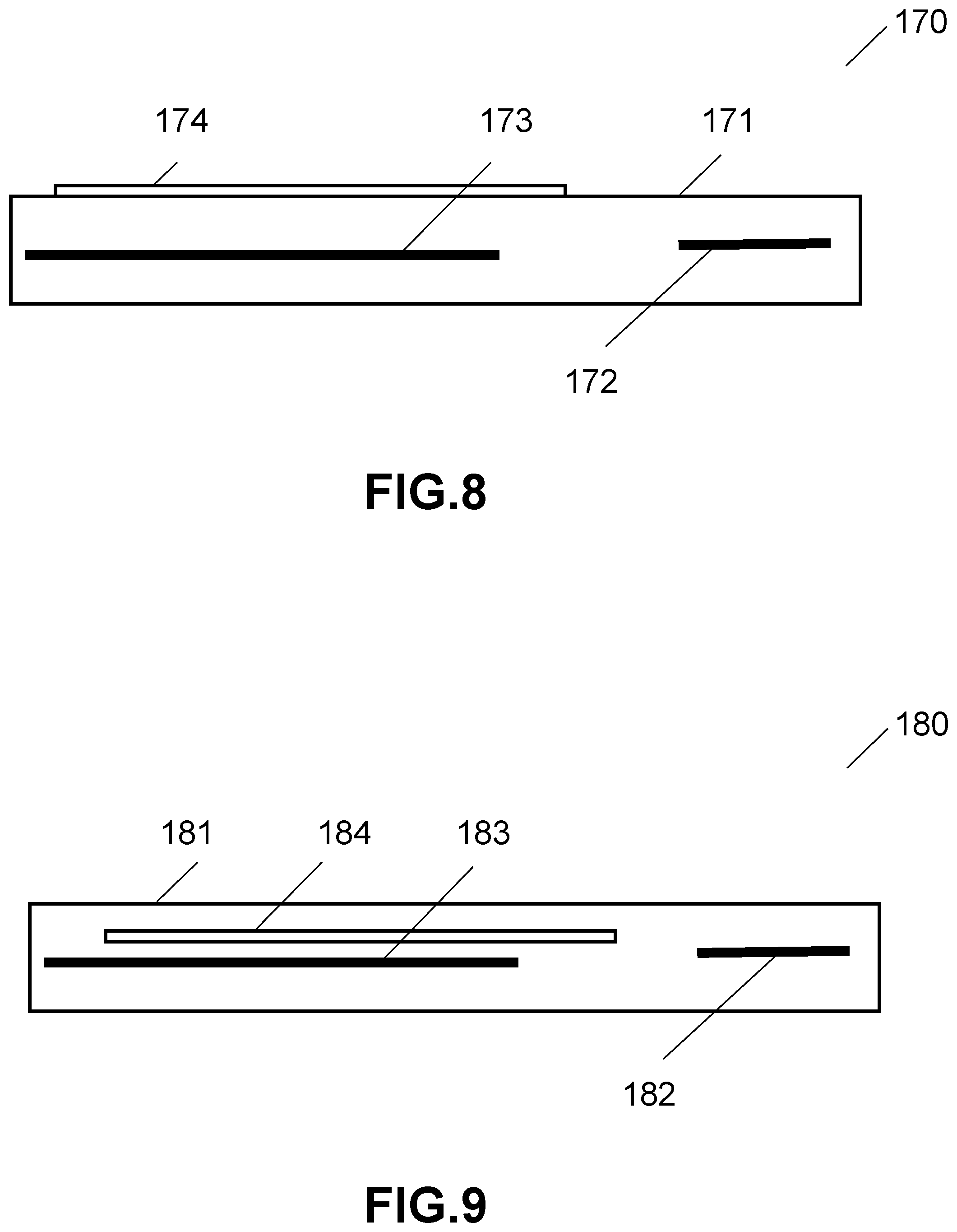
[0108] FIG. 8 provides a schematic cross section view of a detail of a waveguide in which a debanding optic is an optical beam modifying layer disposed on a reflecting surface of the waveguide substrate.
[0109] FIG. 9 provides a schematic cross section view of a detail of a waveguide in which a debanding optic is an optical beam modifying layer disposed within the waveguide substrate.
[0110] FIG. 10 provides a schematic cross section view of a detail of a waveguide in which a debanding optic is an input grating, varying the separation of an input beam from a leading edge of the input grating as a function of the beam incidence angle in one embodiment.
[0111] FIG. 11 provides a schematic cross section view of a detail of a waveguide in which a debanding optic provides projected pupils within the waveguide at locations dependent on the beam incidence angle in one embodiment.
[0112] FIG. 12 provides a schematic cross section view of a detail of a waveguide in which a debanding optic is a partially reflecting layer in one embodiment.
[0113] FIG. 13 provides a schematic cross section view of a detail of a waveguide in which a debanding optic is a polarization rotation layer in one embodiment.
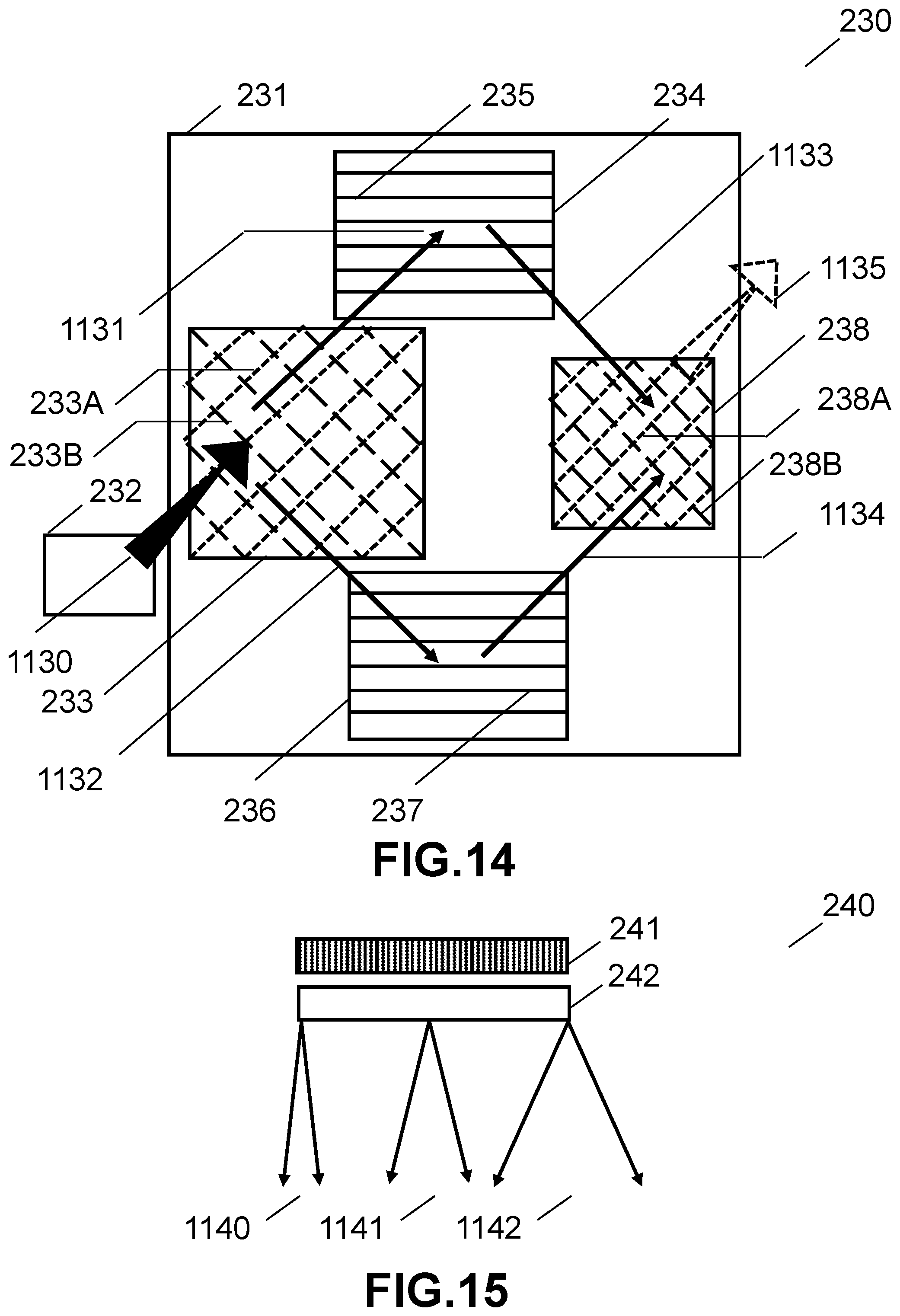
[0114] FIG. 14 provides a schematic plan view of a waveguide in which a debanding optic is a grating that provides separated light paths through the waveguide for different polarizations of the input light in one embodiment.
[0115] FIG. 15 provides a schematic cross section view of a detail of a microdisplay in which a debanding optic provides a variable numerical aperture across principal directions of a microdisplay panel in one embodiment.
[0116] FIG. 16A provides a schematic cross section view of a waveguide using stacked switching input gratings in one embodiment.
[0117] FIG. 16B provides a schematic cross section view of a detail of a waveguide in which a debanding optic is a switchable input grating array in one embodiment.
[0118] FIG. 16C provides a schematic cross section view of a detail of a waveguide in which a debanding optic is an optical beam modifying layer disposed within the waveguide substrate in one embodiment.
[0119] FIG. 16D provides a schematic cross section view of a detail of a waveguide in which a debanding optic is a microdisplay panel that provides a variable numerical aperture across principal directions of in one embodiment.
[0120] FIG. 16E provides a schematic cross section view of a detail of a waveguide in which a debanding optic is a tilted input image generator providing an exit pupil in one embodiment.
[0121] FIG. 16F provides a schematic cross section view of a detail of a waveguide in which a debanding optic a tilted input image generator providing an exit pupil and various projected pupils in one embodiment.
[0122] FIG. 16G provides a schematic cross section view of a detail of a waveguide in which a debanding optic is a tilted input image generator and a coupling prism in one embodiment.
[0123] FIG. 16H provides a schematic cross section view of a detail of a waveguide in which a debanding optic is a plurality of additional substrates having light absorbing edges in one embodiment.
[0124] FIG. 17 provides a schematic cross section view of a detail of a waveguide in which a debanding optic is a plurality of additional substrates having light absorbing edges in one embodiment.
[0125] FIG. 18 provides a schematic cross section view of a detail of a waveguide in which a debanding optic is a tilted input image generator and a coupling prism in one embodiment.
[0126] FIG. 19 provides a schematic cross section of a coating structure for use in balancing color registration in color display in one embodiment.
[0127] FIG. 20 provides a schematic cross section view of a detail of a waveguide in which a debanding optic is an input grating offsetting the input beam cross section from its edge.
DETAILED DESCRIPTION OF THE INVENTION
[0128] Turning now to the drawings, systems and methods relating to near-eye display or head up display systems are shown according to various embodiments. A number of embodiments are directed to waveguide devices for use in near-eye display or head up display systems. A common complication existing in many waveguide devices is banding in the output illumination that affects its uniformity. Accordingly, various embodiments of waveguide devices having uniform output illumination are provided. In numerous embodiments of waveguide devices, a debanding optic is incorporated to eliminate or mitigate banding effects.
[0129] Many embodiments are also directed to holographic waveguide technology that can be advantageously utilized in waveguide devices. In some embodiments, the holographic waveguide technology is used for helmet mounted displays or head mounted displays (HMDs) and head up displays (HUDs). In several embodiments, holographic waveguide technology is used in many applications, including avionics applications and consumer applications (e.g., augmented reality glasses, etc.). In a number of embodiments, an eye is positioned within an exit pupil or an eye box of a display.
[0130] In many embodiments, waveguide devices provide pupil expansion in two orthogonal directions using a single waveguide layer. Uniformity of output is achieved, in accordance with various embodiments, by designing an output grating to have diffraction efficiency varying from a low value near an input end of the waveguide substrate to a high value at the furthest extremity of an output grating. In a number of embodiments, input image data is provided by a microdisplay external to a waveguide optical substrate and coupled to the substrate by means of an input grating. A microdisplay, in accordance with multiple embodiments, is a reflective array and illuminated via a beamsplitter. A reflected image light is collimated such that each pixel of the image provides a parallel beam in a unique direction.
[0131] In accordance with a number of embodiments, a waveguide device is coupling image content into a waveguide efficiently and in such a way that a waveguide image is free from chromatic dispersion and brightness non-uniformity. One way to prevent chromatic dispersion and to achieve better collimation is to use lasers. The use of lasers, however, suffer from pupil banding artifacts which manifest themselves in the output illumination causing disruption of the uniformity of the image. Banding artifacts are able to form when a collimated pupil is replicated (expanded) in a total internal reflection (TIR) waveguide. Banding occurs when some light beams diffracted out of the waveguide each time the beam interacts with the grating exhibit gaps or overlaps, leading to an illumination ripple. The degree of ripple is a function of field angle, waveguide thickness, and aperture thickness. As portrayed in the various embodiments described herein, it was found by experimentation and simulation that the effect of banding can be smoothed by dispersion with broadband sources such as light-emitting diodes (LEDs). LED illumination, however, is not entirely free from the banding problem, particularly for higher waveguide thickness to waveguide input-aperture ratios. Moreover, LED illumination tends to result in bulky input optics and an increase in the thickness of the waveguide device. Accordingly, a number of embodiments of waveguide devices described herein have a compact and efficient debanding optic for homogenizing the light output from holographs to prevent banding distortion.
[0132] Banding effects contribute to non-uniformity of an output illumination. As discovered in several prototype tests, a practical illumination from a waveguide device should achieve less than 20% and preferably not more than 10% non-uniformity to provide an acceptable viewable image. Achieving low non-uniformity requires tradeoffs against other system requirements, particularly image brightness. The tradeoffs are difficult to define in precise terms and are very much dependent on application. Since many optical techniques for reducing non-uniformity generally incur some light loss, output image brightness might be reduced. As the sensitivity of the human visual system to non-uniformity increases with light level, the problem of non-uniformity becomes more acute for displays, such as car HUDs, which require a high luminous flux to achieve high display to background scene contrasts. Accordingly, in some embodiments, extracted light has a spatial non-uniformity less than 10%. In a number of embodiments, extracted light has a spatial non-uniformity less than 20%.
[0133] Several embodiments of the invention will now be further described with reference to the accompanying drawings. For the purposes of explaining the various embodiments of the invention, well-known features of optical technology known to those skilled in the art of optical design and visual displays may have been omitted or simplified in order not to obscure the basic principles of the various embodiments. Description of the various embodiments will be presented using terminology commonly employed by those skilled in the art of optical design. Unless otherwise stated the term "on-axis" in relation to a ray or a beam direction refers to propagation parallel to an axis normal to the surfaces of the optical components described in relation to various devices. In the following description, the terms light, ray, beam and direction may be used interchangeably and in association with each other to indicate the direction of propagation of electromagnetic radiation along rectilinear trajectories. The term light and illumination may be used in relation to the visible and infrared bands of the electromagnetic spectrum. As used herein, the term grating may encompass a grating comprised of a set of gratings in some embodiments.
Waveguide Devices
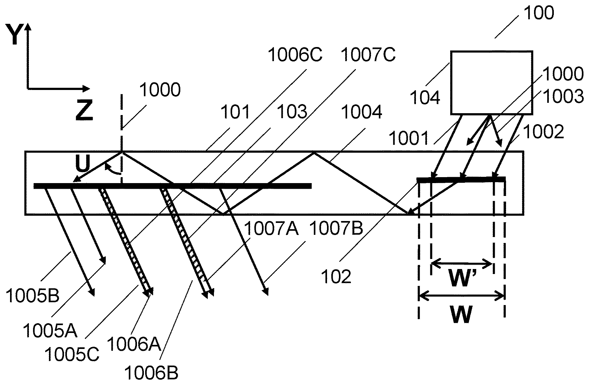
[0134] In accordance with a number of embodiments, a waveguide device includes at least one optical substrate, at least one light source, at least one light coupler to couple the light from the source into the optical substrate, and at least one light extractor to extract the light from the optical substrate to form an output illumination. Depicted in FIG. 1A is an embodiment of a waveguide device. Accordingly, the waveguide device (100) includes at least one optical substrate (101), at least one input grating (102), and at least one output grating (103). The input grating (102), which has a maximum aperture W, couples light (ray arrows 1000-1002), from a light source (104) into a total internal reflection (TIR) path (1004) within the waveguide substrate (101). The input (102) and output (103) gratings as depicted in FIG. 1A may exist in any appropriate configuration, such as the grating configurations described herein.
[0135] In a number of embodiments, a waveguide device includes an input image generator, which further includes an input image generator having a light source, a microdisplay panel, and optics for collimating the light. In the description of some embodiments, an input generator is referred to as a picture generation unit (PGU). In some embodiments, a source may be configured to provide general illumination that is not modulated with image information. In many embodiments, an input image generator projects the image displayed on the microdisplay panel such that each display pixel is converted into a unique angular direction within the substrate waveguide. In various embodiments, collimation optics include at least a lens and mirrors. In many embodiments, lens and mirrors are diffractive. In some embodiments, a light source is at least one laser. In numerous embodiments, a light source is at least one LED. In many embodiments, various combinations of different light sources are used within an input image generator.
[0136] It should be understood that a number of input image generators may be used in accordance with various embodiments of the invention, such as, for example, those described in U.S. patent application Ser. No. 13/869,866 entitled HOLOGRAPHIC WIDE ANGLE DISPLAY and U.S. patent application Ser. No. 13/844,456 entitled TRANSPARENT WAVEGUIDE DISPLAY. In many embodiments, an input image generator contains a beamsplitter for directing light onto the microdisplay and transmitting the reflected light towards the waveguide. In several embodiments, a beamsplitter is a grating recorded in holographic polymer dispersed liquid crystal (HPDLC). In numerous embodiments, a beam splitter is a polarizing beam splitter cube. In some embodiments, an input image generator incorporates a despeckler. Any appropriate despeckler can be used in various embodiments, such as those, for example, described in U.S. Pat. No. 8,565,560 entitled LASER ILLUMINATION DEVICE.
[0137] In a number of embodiments, a light source further incorporates one or more lenses for modifying an illumination beam's angular characteristics. In many embodiments, an image source is a microdisplay or laser-based display. Several embodiments of light sources utilize LEDs, which may provide better uniformity than laser. If laser illumination is used, the risk of illumination banding effects are higher, but may still be eliminated or mitigated in accordance with various embodiments as described herein. In numerous embodiments, light from a light source is polarized. In multiple embodiments, an image source is a liquid crystal display (LCD) microdisplay or liquid crystal on silicon (LCoS) microdisplay.
[0138] In some embodiments, an input image generator optics includes a polarizing beam splitter cube. In many embodiments, an input image generator optics includes an inclined plate to which a beam splitter coating has been applied. In a number of embodiments, an input image generator optics incorporates a switchable Bragg grating (SBG), which acts as a polarization selective beam splitter. Examples of input image generator optics incorporating a SBG are disclosed in U.S. patent application Ser. No. 13/869,866 entitled HOLOGRAPHIC WIDE ANGLE DISPLAY, and U.S. patent application Ser. No. 13/844,456 entitled TRANSPARENT WAVEGUIDE DISPLAY. In many embodiments, an input image generator optics contains at least one of a refractive component and curved reflecting surfaces or a diffractive optical element for controlling the numerical aperture of the illumination light. In multiple embodiments, an input image generator contains spectral filters for controlling the wavelength characteristics of the illumination light. In several embodiments, an input image generator optics contains apertures, masks, filter, and coatings for controlling stray light. In some embodiments, a microdisplay incorporates birdbath optics.
[0139] Returning to an embodiment depicted in FIG. 1A, the external source (102) provides collimated rays in an angular bandwidth (1002). Light in the TIR path (1004) interacts with the output grating (103), extracting a portion of the light each time the TIR light satisfies the condition for diffraction by the grating. In the case of a Bragg grating extraction occurs when the Bragg condition is met. For example, light TIR ray path (1004), which corresponds to the TIR angle U, is diffracted by the output grating into output direction (1005A). It should be apparent from basic geometrical optics that a unique TIR angle is defined by each light incidence angle at the input grating. Light is extracted, and as depicted forms three extraction beams, which are each depicted as flanked by two light rays (1005B & 1005C; 1006A & 1006B; 1007A & 1007B). Perfectly collimated gaps (1006C & 1007C, depicted as cross-hatching) will exit between adjacent beam extracts, resulting in a banding effect. In accordance with a number of embodiments, beam gaps that cause banding are eliminated or minimized by a number of debanding optics as described herein. For example, a debanding optic configures the light such that the input grating has an effective input aperture W that depends on the TIR angle U.
[0140] In a multitude of embodiments, a waveguide device incorporates a debanding optic capable of shifting a pupil to configure the light coupled into the waveguide such that the input grating has an effective input aperture which is a function of the TIR angle. The effect of the debanding optic is that successive light extractions from the waveguide by the output grating integrate to provide a substantially flat illumination profile for any light incidence angle at the input grating. In some embodiments, a debanding optic is implemented by combining various types of optical beam-modifying layers, including (but not limited to) gratings, partially reflecting films, liquid crystal alignment layers, isotropic refractive layers and gradient index (GRIN) structures. It should be understood, that the term "beam-modifying" refers to the variation of amplitude, polarization, phase, and wavefront displacement in 3D space as a function of incidence light angle. In each case, beam-modifying layers, in accordance with several embodiments, provide an effective aperture that gives uniform extraction across the output grating for any light incidence angle at the input grating. In many embodiments, beam-modifying layers are used in conjunction with a means for controlling the numerical aperture of the input light as a function of input angle. In some embodiments, beam-modifying layers are used in conjunction with techniques for providing wavelength diversity.
[0141] FIG. 1B provides a chart illustrating the effect of pupil shifting optics on the light output (labeled I) from the waveguide along a principal propagation direction labeled as Z (referring to the coordinate system shown in FIG. 1A). Intensity profiles (1008A-1008C) for three successive extractions corresponding to an input light direction are shown. The shape of the intensity profiles is controlled by the prescriptions of beam-modifying layers. In a number of embodiments, intensity profiles are integrated to provide a substantially flat intensity profile. For example, the intensity profiles (1008A-1008C) are integrated into a flat profile (1009).
Input Couplers and Extractors Utilized in Waveguide Devices
[0142] Waveguide devices are currently of interest in a range of display and sensor applications. Although much of the earlier work on devices has been directed at reflection holograms, transmission, devices are proving to be much more versatile as optical system building blocks. Accordingly, a number of embodiments are directed to the use of gratings in waveguide devices, which may be used for input or output of pupil. In many embodiments, an input grating is a type of input coupler of light to couple light from a source into a waveguide. In numerous embodiments, an output grating is a type of light extractor of light to extract light from a waveguide to form an output illumination. In several embodiments, waveguide devices utilize a Bragg grating (also referred to as a volume grating). Bragg gratings have high efficiency with little light being diffracted into higher orders. The relative amount of light in the diffracted and zero order can be varied by controlling the refractive index modulation of the grating, a property that is used to make lossy waveguide gratings for extracting light over a large pupil.
[0143] As used herein, the term grating may encompass a grating comprised of a set of gratings in some embodiments. For example, in some embodiments an input grating and/or output grating separately comprise two or more gratings multiplexed into a single layer. It is well established in the literature of holography that more than one holographic prescription can be recorded into a single holographic layer. Methods for recording such multiplexed holograms are well known to those skilled in the art. In some embodiments, an input grating and/or output grating separately comprise two overlapping gratings layers that are in contact or vertically separated by one or more thin optical substrate. In many embodiments, grating layers are sandwiched between flanking glass or plastic substrates. In several embodiments, two or more gratings layers may form a stack within which total internal reflection occurs at the outer substrate and air interfaces. In a number of embodiments, a waveguide device may comprise just one grating layer. In some embodiments, electrodes are applied to faces of substrates to switch gratings between diffracting and clear states. A stack, in accordance with numerous embodiments, further includes additional layers such as beam splitting coatings and environmental protection layers.
[0144] In numerous embodiments, a grating layer is broken up into separate layers. A number of layers are laminated together into a single waveguide substrate, in accordance with various embodiments. In some embodiments, a grating layer is made of several pieces including an input coupler, a fold grating, and an output grating (or portions thereof) that are laminated together to form a single substrate waveguide. In many embodiments, pieces of waveguide devices are separated by optical glue or other transparent material of refractive index matching that of the pieces. In a multitude of embodiments, a grating layer is formed via a cell making process by creating cells of the desired grating thickness and vacuum filling each cell with Switchable Bragg Grating (SBG) material for each of an input coupler, a fold grating, and an output grating. In a number of embodiments, a cell is formed by positioning multiple plates of glass with gaps between the plates of glass that define the desired grating thickness for an input coupler, a fold grating, and an output grating. In many embodiments, one cell may be made with multiple apertures such that the separate apertures are filled with different pockets of SBG material. Any intervening spaces, according to various embodiments, are separated by a separating material (e.g., glue, oil, etc.) to define separate areas. In multiple embodiments, SBG material is spin-coated onto a substrate and then covered by a second substrate after curing of the material. By using a fold grating, a waveguide display advantageously requires fewer layers than previous systems and methods of displaying information according to some embodiments. In addition, by using a fold grating, light can travel by total internal refection within the waveguide in a single rectangular prism defined by the waveguide outer surfaces while achieving dual pupil expansion. In many embodiments, an input coupler and gratings can be created by interfering two waves of light at an angle within the substrate to create a holographic wave front, thereby creating light and dark fringes that are set in the waveguide substrate at a desired angle. In numerous embodiments, a grating in a given layer is recorded in stepwise fashion by scanning or stepping the recording laser beams across the grating area. In some embodiments, gratings are recorded using mastering and contact copying process currently used in the holographic printing industry.
[0145] Input and output gratings, in accordance with many embodiments, are designed to have common surface grating pitch. In some embodiments, an input grating combines a plurality of gratings orientated such that each grating diffracts a polarization of the incident unpolarized light into a waveguide path. In many embodiments, an output grating combines a plurality of gratings orientated such that the light from the waveguide paths is combined and coupled out of the waveguide as unpolarized light. Each grating is characterized by at least one grating vector (or K-vector) in 3D space, which in the case of a Bragg grating is defined as the vector normal to the Bragg fringes. A grating vector determines an optical efficiency for a given range of input and diffracted angles.
[0146] One important class of gratings is known as Switchable Bragg Gratings (SBG), which are utilized in various waveguide devices in accordance with many embodiments. Typically, a holographic polymer dispersed liquid crystal (HPDLC) is used in SBGs. In many embodiments, HPDLC includes a mixture liquid crystal (LC), monomers, photoinitiator dyes, and coinitiators. Often, a mixture also includes a surfactant. The patent and scientific literature contains many examples of material systems and processes that may be used to fabricate SBGs. Two fundamental patents are: U.S. Pat. No. 5,942,157 by Sutherland, and U.S. Pat. No. 5,751,452 by Tanaka et al. Both filings describe monomer and liquid crystal material combinations suitable for fabricating SBG devices. One of the known attributes of transmission SBGs is that the LC molecules tend to align normal to the grating fringe planes. The effect of the LC molecule alignment is that transmission SBGs efficiently diffract P polarized light (i.e., light with the polarization vector in the plane of incidence) but have nearly zero diffraction efficiency for S polarized light (i.e., light with the polarization vector normal to the plane of incidence). Transmission SBGs may not be used at near-grazing incidence as the diffraction efficiency of any grating for P polarization falls to zero when the included angle between the incident and reflected light is small.
[0147] In a number of embodiments, SBGs are fabricated by first placing a thin film of a mixture of photopolymerizable monomers and liquid crystal material between parallel glass plates. One or both glass plates support electrodes for applying an electric field across the film. In numerous embodiments, electrodes are made at least in part by transparent indium tin oxide films. A volume phase grating can then be recorded by illuminating liquid crystal material (often referred to as the syrup) with two mutually coherent laser beams, which interfere to form a slanted fringe grating structure, in accordance with multiple embodiments. During a recording process, monomers polymerize and the mixture undergoes a phase separation, creating regions densely populated by liquid crystal micro-droplets, interspersed with regions of clear polymer, resulting in a HPDLC. In accordance with several embodiments, alternating liquid crystal-rich and liquid crystal-depleted regions of an HPDLC device form fringe planes of a grating. A resulting volume phase grating can exhibit very high diffraction efficiency, which may be controlled, in accordance with various embodiments, by the magnitude of the electric field applied across the film. When an electric field is applied to a grating via transparent electrodes, a natural orientation of the LC droplets is changed, reducing the refractive index modulation of the fringes and dropping a hologram diffraction efficiency to very low levels. Typically, SBG Elements are switched clear in 30 .mu.s, with a longer relaxation time to switch ON. Note that the diffraction efficiency of a device can be adjusted, in accordance with many embodiments, by means of applied voltage over a continuous range. A device exhibits near 100% efficiency when no voltage is applied and near-zero efficiency when a sufficiently high voltage is applied. In certain embodiments, of HPDLC devices, magnetic fields may be used to control the LC orientation. In certain embodiments of HPDLC devices, phase separation of LC material from polymer may be accomplished to such a degree that no discernible droplet structure results. In a number of embodiments, a SBG is also used as a passive grating, which may provide a benefit of a uniquely high refractive index modulation.
[0148] According to numerous embodiments, SBGs are used to provide transmission or reflection gratings for free space applications. Various embodiments of SBGs are implemented as waveguide devices in which the HPDLC forms either the waveguide core or an evanescently coupled layer in proximity to the waveguide. In many embodiments, parallel glass plates used to form the HPDLC cell provide a total internal reflection (TIR) light guiding structure. Light is coupled out of a SBG, in accordance with several embodiments, when a switchable grating diffracts light at an angle beyond the TIR condition.
[0149] In many embodiments of waveguide devices based on SBGs, gratings are formed in a single layer sandwiched by transparent substrates. In a number of embodiments, a waveguide is just one grating layer. In various embodiments that incorporate switchable gratings, transparent electrodes are applied to opposing surfaces of the substrate layers sandwiching the switchable grating. In some embodiments, cell substrates are fabricated from glass. An exemplary glass substrate is standard Corning Willow glass substrate (index 1.51), which is available in thicknesses down to 50 microns. In a number of embodiments, cell substrates are optical plastics.
[0150] It should be understood that Bragg gratings could also be recorded in other materials. In several embodiments, SBGs are recorded in a uniform modulation material, such as POLICRYPS or POLIPHEM having a matrix of solid liquid crystals dispersed in a liquid polymer. In multiple embodiments, SBGs are non-switchable (i.e., passive). Non-switchable SBGs may have the advantage over conventional holographic photopolymer materials of being capable of providing high refractive index modulation due to its liquid crystal component. Exemplary uniform modulation liquid crystal-polymer material systems are disclosed in United State Patent Application Publication No. US2007/0019152 by Caputo et al and PCT Application No.: PCT/EP2005/006950 by Stumpe et al. both of which are incorporated herein by reference in their entireties. Uniform modulation gratings are characterized by high refractive index modulation (and hence high diffraction efficiency) and low scatter. In many embodiments, at least one grating is a surface relief grating. In some embodiments at least one grating is a thin (or Raman-Nath) hologram.
[0151] In multiple embodiments, gratings are recorded in a reverse mode HPDLC material. Reverse mode HPDLC differs from conventional HPDLC in that the grating is passive when no electric field is applied and becomes diffractive in the presence of an electric field. Reverse mode HPDLC may be based on any of the recipes and processes disclosed in PCT Application No.: PCT/GB2012/000680, entitled IMPROVEMENTS TO HOLOGRAPHIC POLYMER DISPERSED LIQUID CRYSTAL MATERIALS AND DEVICES. A grating may be recorded in any of the above material systems, in accordance of various embodiments, but used in a passive (non-switchable) mode. The fabrication process is identical to that used for switchable gratings, but with an electrode coating stage being omitted. LC polymer material systems are highly desirable in view of their high index modulation. In some embodiments, gratings are recorded in HPDLC but are not switchable.
[0152] In some embodiments, a grating encodes optical power for adjusting the collimation of the output. In many embodiments, an output image is at infinity. In numerous embodiments, an output image may be formed at distances of several meters from an eye box.
[0153] In several embodiments, an input grating may be replaced by another type of input coupler. In particular embodiments, an input grating is replaced with a prism or reflective surface. In a number of embodiments, an input coupler can be a holographic grating, such as a switchable or non-switchable SBG grating. The input coupler is configured to receive collimated light from a display source and to cause the light to travel within the waveguide via total internal reflection between the first surface and second surfaces.
[0154] It is well established in the literature of holography that more than one holographic prescriptions can be recorded into a single holographic layer. Methods for recording such multiplexed holograms are well known to those skilled in the art. In some embodiments, at least one of an input or output grating combines two or more angular diffraction prescriptions to expand the angular bandwidth. In many embodiments, at least one of the input or output gratings combines two or more spectral diffraction prescriptions to expand the spectral bandwidth. In numerous embodiments, a color multiplexed grating is used to diffract two or more primary colors.
[0155] Many embodiments, as described herein, are operated in monochrome. A color waveguide, however according to various embodiments of the invention, includes a stack of monochrome waveguides. In a number of embodiments, a waveguide device uses red, green and blue waveguide layers. In several embodiments, a waveguide device uses red and blue/green layers. In some embodiments, gratings are all passive, that is, non-switchable. In multiple embodiments, at least one grating is switchable. In a number of embodiments, input gratings in each layer are switchable to avoid color crosstalk between waveguide layers. In some embodiments, color crosstalk is avoided by disposing dichroic filters between the input grating regions of the red and blue and the blue and green waveguides.
[0156] In a number of embodiments, light is characterized by a wavelength bandwidth. In many embodiments, a waveguide device is capable of diversifying the wavelength bandwidth of light. In accordance to various embodiments, Bragg gratings, which are inherently spectral bandwidth limited devices, are most efficiently utilized with narrow band sources such as LEDs and lasers. A Bragg grating, in accordance to many embodiments, diffracts two different wavelength bands with high efficiency when the grating prescription and the incident light ray angles satisfy the Bragg equation. Full color waveguides, in accordance to multiple embodiments, utilize separate specific wavelength layers, such as, red, green and blue diffracting waveguide layers. Two-layer solutions in which one layer diffracts two of the three primary colors are used in numerous embodiments. In many embodiments, a natural spectral bandwidth of a Bragg grating is adequate for minimizing color cross talk. For tighter control of color crosstalk, however, additional components such as dichroic filters and narrow band filters integrated between waveguide layers and, typically, overlapping the input gratings may be used.
Debanding Optics
[0157] In numerous embodiments, a debanding optic is an effective input aperture such that when the optical substrate has a thickness D, the input aperture is configured to provide a TIR angle U in the optical substrate, and the angle U is calculated by 2D tan (U). Provided in FIG. 2 is an embodiment of a waveguide device (110) incorporating a debanding optic in a form of a waveguide that includes a waveguide substrate (111) and a TIR (1012) such that a condition of zero banding exists. In many embodiments, a condition of zero banding, that is no gaps between successive light extractions along the TIR ray path, occurs when the effective input aperture for a TIR angle U and a waveguide substrate thickness D is given by 2D tan (U).
[0158] In some embodiments, a debanding optic provides spatial variation of the light along a TIR path of at least one of diffraction efficiency, optical transmission, polarization or birefringence. A typical spatial variation (120) is provided in the chart FIG. 3 by the curve (1020) where the Y-axis refers to the value of any of the above parameters (e.g., diffraction efficiency) and X-axis is a beam propagation direction within the waveguide. In a number of embodiments, a spatial variation is in two dimensions (in the plane of the waveguide).
[0159] In some embodiments, a debanding optic is at least one grating configured to have multiple gratings, such that each grating provides a small pupil shift to eliminate or mitigate banding. In many embodiments, a stack of multiple gratings achieves a small pupil shift when separations between the gratings within the stack are designed to provide a pupil shift for each angle. In a number of embodiments, gratings capable of a pupil shift are separated by transparent substrates. In several embodiments, gratings capable of a pupil shift are passive. Alternatively, in some embodiments, gratings are switched on when a voltage is applied. In some embodiments, multiple gratings arranged to have lateral relative displacements provides a pupil shift. In numerous embodiments, multiple gratings are configured in a two-dimensional array with different sub arrays of grating elements being switched in to their diffraction states according to an incidence angle. In some embodiments, gratings are configured as stacks of arrays. In various embodiments, separate gratings are provided for different wavelength bands. In a number of embodiments, a grating is multiplexed.
[0160] In many embodiments, gratings have grating parameters that vary across the principal plane of a waveguide. In some embodiments, a diffraction efficiency is varied to control the amount of light diffracted versus the amount of light transmitted down the waveguide as zero order light, thereby enabling the uniformity of light extracted from the waveguide to be fine-tuned. In several embodiments, K-vectors of at least one grating has rolled K-vectors which have directions optimized to fine tune the uniformity of light extracted from the waveguide. In various embodiments, an index modulation of gratings is varied to fine tune the uniformity of light extracted from the waveguide. In numerous embodiments, a thickness of the gratings is varied to fine tune the uniformity of light extracted from the waveguide.
[0161] In a number of embodiments, a debanding optic is at least one grating configured as a stacked switchable grating that turns on when a voltage is applied, shifting pupil to eliminate or mitigate banding effects. Depicted in FIG. 4 is an embodiment of a waveguide device (130) with an optical substrate (131) having stacked switchable input gratings (132A & 1326) and a non-switchable output grating (133). A voltage supply (134) is coupled to the input gratings (132A & 1326) by an electrical connection (135A & 1356) to switch on the input gratings (132A & 132B) to provide pupil shift. Depicted in FIG. 5 is an embodiment of a waveguide device (141) having a non-switchable input grating and a switchable output gating having stacked grating layers (143A & 143B). A voltage supply (144) is coupled to the output gratings (143A & 143B) by an electrical connection (145A & 145B) to switch on the output gratings (143A & 143B) to provide a pupil shift. In various embodiments, a thin substrate layer exits between stacked gratings to provide at least some separation.
[0162] In some embodiments, a debanding optic is at least one grating configured as an array of switchable grating elements that can turn on a specific element when a voltage is applied, shifting pupil to eliminate or mitigate banding effects. Depicted in FIG. 6A is an embodiment of a waveguide device (150) having an optical substrate (151) that contains input gratings (152A & 152B) each having a plurality of grating elements (153A-156A & 153B-156B) and an output grating (157). The waveguide device further includes a voltage supply (158) coupled to each input grating (152A & 152B) by an electrical connection (159A & 159B) configured to individually switch on each element (e.g., 156A & 156B) to shift pupil. Although not depicted, it should be understood that a voltage supply can be connected to each and every element to create an array of switchable elements. Furthermore, although FIG. 6A only depicts an input grating configured to be an array, it should be understood that an output grating can also be an array of elements, each element configured to be switchable, in accordance with a number of embodiments of the invention.
[0163] In various embodiments, a grating has a plurality of rolled K-vectors. A K-vector is a vector aligned normal to the grating planes (or fringes) which determines the optical efficiency for a given range of input and diffracted angles. Rolling K-vectors, in accordance with a number of embodiments, allows an angular bandwidth of a grating to be expanded without the need to increase the waveguide thickness. Depicted in FIG. 6B is an embodiment of a grating (152C) having four rolled K-vectors (K1-K4). In a number of embodiments, a grating is configured as a two-dimensional array of switchable elements. For example, depicted in FIG. 7, a grating is configured as a two-dimensional array (160) of switchable elements (e.g., 161).
[0164] In numerous embodiments, a debanding optic is at least one grating configured to be a plurality of passive grating layers configured to shift pupil to eliminate or mitigate banding effects. When a waveguide device incorporates multiple passive grating layers, in accordance with various embodiments, the basic architecture is similar to some of the embodiments that incorporate active grating layers (e.g., see FIGS. 4 & 5) but without a voltage supply. In some embodiments, it is advantageous to use SBGs in non-switchable mode to take advantage of the higher index modulation afforded by a number of liquid crystal polymer material systems. In many embodiments, a debanding optic is at least one multiplexed grating configured to shift pupil to eliminate or mitigate banding effects.
[0165] In some embodiments, a waveguide device includes a fold grating for providing exit pupil expansion. It should be understood that various fold gratings may be used in accordance with various embodiments of the invention. Examples of various fold gratings that may be used in a multitude of embodiments are disclosed in PCT Application No. PCT/GB2016000181 entitled WAVEGUIDE DISPLAY or as described in other references cited herein. A fold grating, in accordance of several embodiments, incorporates multiple gratings for pupil shifting to eliminate or mitigate banding effects, with each grating providing a small pupil shift.
[0166] In many embodiments, a debanding optic is one or more index layers disposed within an optical substrate such that the one or more index layers influences the light ray paths within the optical substrate as a function of at least one of ray angle or ray position, shifting pupil to mitigate banding effects. In some embodiments, at least one index layer is a GRIN medium. It should be understood that various GRIN mediums may be used in accordance with various embodiments of the invention, such as the examples of various GRIN mediums that are described in U.S. Provisional Patent Application No. 62/123,282 entitled NEAR EYE DISPLAY USING GRADIENT INDEX OPTICS and U.S. Provisional Patent Application No. 62/124,550 entitled WAVEGUIDE DISPLAY USING GRADIENT INDEX OPTICS.
[0167] In a number of embodiments, a debanding optic is one or more index layers disposed adjacent to at least one reflecting surface of an edge of an optical substrate such that the one or more layers are configured to provide pupil shifting to eliminate or mitigate banding effects. Depicted in FIG. 8 is an embodiment of a waveguide device (170) having an optical substrate (171) that contains an input grating (172) and an output grating (173) with one or more stacked index layers (174) disposed adjacent an upper reflecting surface of the waveguide such that the one or more index layers provide pupil shifting. In many embodiments, a debanding optic is one or more index layers disposed within an optical substrate such that the one or more layers are configured to provide pupil shifting to eliminate or mitigate banding effects. For example, depicted in FIG. 9 is an embodiment of a waveguide device (180) having an optical substrate (181) that contains an input grating (182) and an output grating (183) with one or more stacked index layers (184) disposed within the optical substrate (181) such that the one or more layers (184) are configured to provide pupil shifting. In some embodiments, a waveguide device incorporates a debanding optic that includes one or more index layers disposed within an optical substrate and one or more index layers also disposed adjacent to at least one reflecting surface of the optical substrate.
[0168] In several embodiments, a debanding optic is an input grating having a leading edge able to couple incident light such that a unique displacement of a ray bundle of the light relative to the leading edge of the input grating is provided by the input grating for any given incident light direction, shifting pupil to eliminate or mitigate banding effects. Depicted in FIG. 10 is a detail of an embodiment of a waveguide device (190) having an optical substrate (191) that contains an input grating (192) with a leading edge (193). Collimated input ray paths for two different input angles (1090 & 1091) and the corresponding diffracted rays (1092 & 1093) are depicted. Separations of edges of the two ray sets from the leading edge of the input gratings (1094 & 1095) are depicted. In some embodiments, a displacement of light relative to an edge of an input grating of a ray bundle results in a portion of the beam to fall outside the input grating apertures and therefore not being diffracted into a TIR path inside an optical substrate, depending on the field angle of the incoming light. A suitable absorbing film traps non-diffracted light, in accordance with various embodiments. Hence a beam width can be tailored to meet a debanding condition, when a TIR angle U and a waveguide substrate thickness D is given by 2D tan (U), as was described in greater detail in relation to FIG. 2. An example of such an embodiment will be discussed in greater detail in a subsequent section (see FIG. 20).
[0169] In many embodiments, a debanding optic is an input grating configured to have a variation of diffraction efficiencies such that a plurality of collimated incident ray paths of the incident light is diffracted into different TIR ray paths, as determined by a ray path input angle, such that a projected pupil is capable of forming at a unique location within the optical substrate for each of the plurality of collimated incident ray paths to eliminate or mitigate banding effects. Depicted in FIG. 11 is a detail of an embodiment of a waveguide device (200) having an optical substrate (201) that contains an input grating (202). Collimated input ray paths for two different input angles (1100 &1101) are diffracted by the input grating (202) such that the diffracted rays (1102 & 1103) each follow a TIR path down the optical substrate (201). Each TIR ray path (1104 & 1105) forms a projected pupil (1106 & 1107) in a unique location, based on the incident angle, and such that banding effects are eliminated and/or mitigated.
[0170] In some embodiments, a variation of diffraction efficiencies varies along a principal waveguide direction to provide, at least in part, pupil shift to eliminate or mitigate banding effects. In many embodiments, a variation of diffraction efficiencies varies in two dimensions over the aperture of the input grating.
[0171] In some embodiments, a debanding optic is a partially reflecting layer disposed within an optical substrate such that the partially reflecting layer separates incident light into transmitted and reflected light, shifting pupil to eliminate or mitigate banding effects. Depicted in FIG. 12 is a detail of an embodiment of a waveguide device (210) having an optical substrate (211) that contains a partially reflecting layer (212), capable of separating incident light (1110) into transmitted light (1000) and reflected light (1111). Transmitted and reflected light (1000 & 1111) each follow a TIR path along a waveguide substrate (211), resulting in a pupil shift to eliminate or mitigate banding effects.
[0172] In numerous embodiments, a debanding optic is a polarization modifying layer disposed within an optical substrate such that the polarization modifying layer separates incident light into transmitted and reflected light, shifting pupil to eliminate or mitigate banding effects. For example, FIG. 13 provides a detail of an embodiment of a waveguide device (220) having an optical substrate (221) that contains a partially reflecting polarization modifying layer (222), which separates incident light (1120) having a polarization vector (1123) into transmitted light (1121) having a polarization vector (1124), resulting from the retarding effect of a polarization modifying layer (222), and reflected light (1122). Transmitted (1121) and reflected light (1122) follow TIR paths down the optical substrate (221) resulting in a pupil shift to eliminate or mitigate banding effects. In some embodiments, a polarization modifying layer is formed by stretching a polymeric material in at least one dimension. In particular embodiments, a polarization modifying layer is a polymeric material, such as birefringent polyester, polymethylmethacrylate (PMMA), or poly-ethylene terephthalate (PET). Polymeric materials may be used in a single layer or two or more may be combined in a stack.
[0173] In many embodiments, a debanding optic is at least one grating configured to provide at least two separate waveguide paths which cancel non-uniformity of light of the extracted light for any incidence light angle, eliminating or mitigating banding effects. In several embodiments, a debanding optic includes at least one grating having crossed slant gratings used in conjunction with at least one fold grating exit pupil expander configured to provide a pupil shift to eliminate or mitigate banding effects. Depicted in FIG. 14 is an embodiment of a waveguide device (230) having an optical substrate (231) coupled to an input image generator (232). The optical substrate (231) contains an input grating (233) with crossed slant gratings (233A & 233B), a first fold grating exit pupil expander (234) containing a grating (235), a second fold grating exit pupil expander (236) containing a grating (237), and an output grating (238) with crossed slant gratings (238A & 238B). The input grating (233) receives light from the input image generator (232) in a direction (1130), such that the direction is normal to the surface of the input grating (233). In numerous embodiments, crossed gratings in a grating have a relative angle of approximately ninety degrees in the plane of an optical substrate. It should be noted, however, other angles may be used in practice and still fall within various embodiments of the invention.
[0174] In several embodiments, a debanding optic is a system of gratings, such that an input grating and an output grating each combine crossed gratings with peak diffraction efficiency for orthogonal polarizations states. In some embodiments, polarization states created by input and output gratings are S-polarized and P-polarized. In a number of embodiments, polarization states created by input and output gratings are opposing senses of circular polarization. Several embodiments utilize gratings recorded in liquid crystal polymer systems, such as SBGs, which may have an advantage owing to their inherent birefringence and exhibiting strong polarization selectivity. It should be noted, however, that other grating technologies that can be configured to provide unique polarization states may be used and still fall within various embodiments of the invention.
[0175] Returning to FIG. 14, a first polarization component of the input light incident on the input grating (233) along a direction (1130) is directed by a grating (233B) into a TIR path along a direction (1131) and a second polarization component is directed by a second grating (233A) into a second TIR path along a direction (1132). Light traveling along the TIR paths (1131 &1132) is expanded in the plane of the optical substrate (231) by fold gratings (234 & 236) and diffracted into second TIR paths (1133 & 1134) towards an output grating (238). Crossed slants (238A & 238B) of the output grating (238) diffract light from the second TIR paths (1133 & 1134) into a uniform output path (1135) such that banding effects are eliminated or mitigated. In some embodiments, a grating prescription is designed to provide dual interaction of guided light with the grating, which may enhance a fold grating angular bandwidth. A number of embodiments of dual interaction fold gratings can be used, such as the gratings described in U.S. patent application Ser. No. 14/620,969 entitled WAVEGUIDE GRATING DEVICE.
[0176] In several embodiments, a debanding optic is an optical component within a microdisplay that provides variable effective numerical apertures (NA) capable of being spatially varied along at least one direction to shift pupil to eliminate or mitigate banding effects. Depicted in FIG. 15 is an embodiment an input image generator (240) designed to have a numerical aperture (NA) variation ranging from high NA on one side of the microdisplay (241) panel varying smoothly to a low NA at the other side to provide a pupil shift. For the purposes of explanation, a NA in relation to a microdisplay is defined herein as being proportional to the sine of the maximum angle of the image ray cone from a point on the microdisplay surface with respect to an axis normal to the microdisplay. As shown in FIG. 15, the NA of the microdisplay (241) is spatially varied by an optical component (242) which causes the NA to vary across at least one principal dimension of the microdisplay as indicated by the extending light rays (1140-1142). It should be understood that an optical component used to vary a NA may be any appropriate optical component, such as any of the optical components described in PCT Application No.: PCT/GB2016000181 entitled WAVEGUIDE DISPLAY. In multiple embodiments, a microelectromechanical systems (MEMS) array is used to spatially vary the (NA) across a microdisplay display panel. In numerous embodiment, a MEMs array spatially varies the NA of light reflected from a microdisplay panel. In many embodiments, a MEMS array utilizes technology used in data projectors.
[0177] In several embodiments, a microdisplay is a reflective device. In some embodiments, a microdisplay is a transmission device, such as, for example, a transmission liquid crystal on silicon (LCoS) device. In many embodiments, an input image generator has a transmission microdisplay panel with a backlight and a variable NA component. When a backlight is employed, in accordance with various embodiments, the illuminated light typically has a uniform NA across, illuminating a back surface of a microdisplay, which is propagated through a variable NA component and converted into an output image modulated light with NA angles varying along a principal axis of the microdisplay.
[0178] In a number of embodiments, an emissive display is employed in a microdisplay. Examples of emissive displays for use within a microdisplay include, but not limited to, LED arrays and light emitting polymers arrays. In some embodiments, an input image generator incorporates an emissive microdisplay and a spatially-varying NA component. Light from a microdisplay employing an emissive display, in accordance with various embodiments, typically has a uniform NA across the emitting surface of the display, illuminates the spatially-varying NA component and is converted into an output image modulated light with NA angles varying across the display aperture.
[0179] In many embodiments, a debanding optic is a plurality of grating layers within at least one grating such that the plurality of grating layers is configured to smear out any fixed pattern noise resulting in pupil shift to eliminate or mitigate banding effects. Depicted in FIG. 16A is an embodiment of a waveguide device (250) having a picture generation unit (PGU) (251), optically coupled to an optical substrate (252) that extracts light via an output grating (253). The optical substrate (252) contains stacked input gratings (254 & 255) and a fold grating that is not illustrated. Input light (1150) from the PGU (251) is coupled into the waveguide substrate (252) by the input gratings (254 & 255), smearing out any fixed pattern noise, and diffracted into TIR paths (1151), and then diffracted into extracted light (1152) by the output grating (253) resulting in a pupil shift to eliminate or mitigate banding effects. In some embodiments, multiple gratings are combined into a multiplexed grating.
[0180] In several embodiments, a debanding optic is the input grating configured as an array of selectively switchable elements such that configuring the input grating as a switching grating array provides pupil switching in vertical and horizontal directions to shift pupil to eliminate or mitigate banding effects. In many embodiments, individual grating elements are designed to diffract light incident in predefined input beam angular ranges into corresponding TIR angular ranges. Depicted in FIG. 16B is an embodiment of a waveguide device (260) having a PGU (261), optically coupled to an optical substrate (262) that extracts light via an output grating (253). The optical substrate (262) contains a switchable input grating array (264) of selectively switchable elements (265). Input light (1160) is coupled into the optical substrate (262) by the input grating (264), which provides pupil shift in vertical and horizontal directions that is diffracted into TIR paths (1161), and then diffracted into extracted light (1162) by the output grating (263) with banding effects eliminated or mitigated.
[0181] In numerous embodiments, a debanding optic is a plurality of refractive index layers that provide spatial variation along each TIR path of at least one of diffraction efficiency, optical transmission, polarization and birefringence to influence ray paths within a waveguide substrate as a function of at least one of ray angle or ray position within the substrate, resulting in shift of pupil to eliminate or mitigate banding effects. In several embodiments, a plurality of refractive index layers incorporates adhesives of different indices, especially to influence high angle reflections. In some embodiments, a plurality of refractive index layers incorporate layers, such as alignment layers, isotropic refractive layers, GRIN structures, antireflection layers, partially reflecting layer, or birefringent stretched polymer layers. Depicted in FIG. 16C is an embodiment of a waveguide device (270) having a PGU (271) optically coupled to an optical substrate (272) that extracts light via an output grating (273). The optical substrate (272) contains an input grating (274) and at least one refractive index layer (275). Input light (1170) is coupled into the optical substrate (272) by the input grating (275) and diffracted into TIR paths (1171) that pass through the refractive index layer (275) causing spatial variation, and then diffracted into extracted light (1172) by the output grating (273), resulting in a pupil shift to eliminate or mitigate banding effects.
[0182] In some embodiments, a debanding optic is a microdisplay projecting spatially varied NAs that shift pupil to eliminate or mitigate banding effects. In several embodiments, NA can be varied in two orthogonal directions. Depicted in FIG. 16D is an embodiment of a waveguide device (280) having a PGU (281) optically coupled to an optical substrate (282) that extracts light via an output grating (283). The optical substrate (282) contains an input grating (285). Input light (1180) is coupled into the optical substrate (282) by the input grating (285) and diffracted into TIR paths (1181), and then diffracted into extracted light (1182) by the output grating (283). The PGU (281) has a microdisplay (286) overlaid by an NA modification layer (287) capable of spatially varying NA and modifying the light into varying beam profiles (1184-1186), resulting in pupil shift to eliminate or mitigate banding effects. In accordance with various embodiments, a PGU also incorporates other components, such as a projection lens and/or beamsplitter, for example.
[0183] In many embodiments, a debanding optic is a tilted microdisplay configured to project a tilted, rectangular exit pupil such that the cross section of the exit pupil varies with a field angle, such that banding effects are eliminated or mitigated. In a number of embodiments, an exit pupil changes position on an input grating. This technique, in accordance with various embodiments, can be used to address banding in one beam expansion axis. Depicted in FIG. 16E is an embodiment of a waveguide device (290) having a PGU (291) optically coupled to an optical substrate (292) which extracts light via an output grating (293). Input light (1190) emerging from the tilted PGU exit pupil (295) is coupled into the waveguide via an input grating (294) and diffracted into TIR paths (1191), and then diffracted into extracted light (1192) by the output grating (293), eliminating or mitigating banding effects.
[0184] In several embodiments, a debanding optic is a tilted microdisplay configured to angle light rays to form various projected pupils at different positions along an optical substrate for each direction of incident light, such that banding effects are mitigated along one expansion axis. Depicted in FIG. 16F is an embodiment of a waveguide device (300) having a PGU (301) optically coupled to an optical substrate (302), which extracts light via an output grating (303). Input light (1200) emerging from the tilted PGU exit pupil (305) is coupled into the waveguide by an input grating (304) and diffracted into TIR paths (1201). The guided light forms beam angle-dependent projected pupils (1203-1205) at different positions along the substrate (302) for each direction of incident light, and then diffracted into extracted light (1202) by the output grating (303), eliminating or mitigating banding effects.
[0185] In numerous embodiments, a debanding optic is a prism coupled to an optical substrate, such that a linear relationship between the angles of an exit pupil from a light source and the TIR angles in the optical substrate result in no gaps between successive light extractions along the TIR ray path, which occurs when the TIR path angle is U as defined by 2D tan (U). In many embodiments, an input grating is replaced with a coupling prism. In several embodiments, input light is provided through a tilted PGU pupil. By selecting a prism angle and cooperative PGU pupil tilt, in accordance with various embodiments, it is possible to achieve an approximately linear relationship between the angles out of the PGU exit pupil and the TIR angles in the waveguide while meeting a debanding condition when the effective input aperture for a TIR angle U and a waveguide substrate thickness D is given by 2D tan (U), over the entire field of view range. Depicted in FIG. 16 G is an embodiment of a waveguide device (310) having a PGU (311) optically coupled to an optical substrate (312), which extracts light via an output grating (313). Input light (1210) emerging from a tilted PGU exit pupil (315) is coupled into the optical substrate (312) by a prism (314) resulting in TIR paths (1211) and then diffracted into extracted light (1192) by the output grating (293), eliminating or mitigating banding effects. In some embodiments, color dispersion due to the prism is compensated by a diffractive surface. In many embodiments, a prism coupler has refracting surface apertures designed to shape the light as a function of angle. Light at the edges of the beam that is not transmitted through the prism into the waveguide is eliminated from the main light path by baffling or light absorbing coatings, in accordance with a number of embodiments.
[0186] In some embodiments, a debanding optic is a light-absorbing film adjacent to the edges of an optical substrate such that portions of incident light, that would otherwise give rise to banding, are removed, eliminating or mitigating banding effects. Depicted in FIG. 16H is an embodiment of a waveguide device (320) designed for beam shifting along one axis of beam expansion. The waveguide device has a PGU (321) coupled to a waveguide (322) containing an output grating (323) and an input grating (324), a substrate (325) having a light-absorbing film (326) applied to one of its edges, a substrate (327) having a light-absorbing film (328) applied to one its edges, the substrates (325 & 327) sandwiching the portion of the waveguide (322) that contains the input grating. The input ray at the upper limit of the input beam (1221) is diffracted by the input grating (324) into a TIR path (1223) and absorbed by the light-absorbing film (326) applied to the substrate (325), eliminating or mitigating banding effects. An input ray at the lower limit of the input beam (1222) is diffracted by the input grating (32) into a TIR path (1224) and absorbed by the light-absorbing film (328) applied to the substrate (327), eliminating or mitigating banding effects. An input ray near the central portion of the input beam (1220) is diffracted by the input grating (324) into a TIR path (1225) which does not interact with either of the light-absorbing films (326 & 328) and continues to propagate under TIR until it is extracted by the output grating (323) into the output beam (1226).
[0187] In many embodiments, a debanding optic is a first light-absorbing film disposed adjacent to the edges an input substrate containing an input grating and disposed adjacent to an optical substrate, and a second light-absorbing film disposed adjacent to the edges a second substrate, attached adjacent to the optical substrate opposite the input substrate, such that incident light results in no gaps between successive light extractions along the TIR ray path, which occurs when the TIR path angle is U as defined by 2D tan (U). Depicted in FIG. 17 is an embodiment of a waveguide device (330) configured such that an input grating (334) is disposed within an input substrate (333), which together with the substrate (332) sandwiches a waveguide (331). The cross section of an input beam for a given field of view direction (1230) with peripheral rays (1231 & 1232) enters into the input grating (334). An input beam portion bounded by rays (1233 & 1234) is diffracted into a beam path (1236) and intercepted by an absorbing film (335) applied to the edge of the upper substrate (332). The input beam portion bounded by rays (1232 & 1235) is diffracted into the beam path (1237) undergoes TIR at the outer surface of the upper substrate (332) and intercepted by an absorbing film (336) applied to the input substrate edge. The input beam portions bounded by rays (1231 & 1233) and (1234 & 1235) are diffracted into respective TIR paths (1239 &1240) and (1241 & 1242) which exhibit no gap or overlap in the beam cross section region (1243) and at all beam cross sections thereafter, thereby eliminating banding utilizing a TIR angle U and a waveguide substrate thickness D is given by 2D tan (U). In some particular embodiments, the thickness of a waveguide is 3.4 mm, the thickness of an upper substrate 0.5 mm, and a lower substrate contains two 0.5 mm thick glass substrates sandwiching an input grating. Based on this geometry and the debanding condition of a TIR angle U and a waveguide substrate thickness D is given by 2D tan (U), the throughput efficiency is estimated to be roughly 1-2*0.5/(2*3.4)=84% with some small variation across the field of view.
[0188] In some embodiments utilizing an input substrate, an input grating is implemented in separate cells bonded to the main waveguide, thus simplifying indium tin oxide (ITO) coating. In many embodiments utilizing an input substrate, beam shifting techniques based on forming a projected stop and tilting the PGU exit pupil are incorporated, to provide debanding in orthogonal directions.
[0189] Depicted in FIG. 18 is a detail of an embodiment of a waveguide device 340 having a waveguide portion (341), a prism (342) with two refracting faces inclined at a relative angle (1250) and an exit pupil (343) of a PGU (not pictured), the exit pupil (343) tilted at an angle (1251) relative to a reference axis (1252).
[0190] In some embodiments, a prism is separated from a waveguide by a small air gap. In many embodiments, a prism is separated from a waveguide by a thin layer of low index material.
[0191] Returning to FIG. 18, light beams (1253 & 1254) from the exit pupil (343) correspond to two different field angles refracted through the prism (342) as beams (1255 & 1256) and are then coupled into the TIR paths (1257 & 1258) inside the waveguide (341). The beam widths at the waveguide surface adjacent the prism (1259A & 1259B) are depicted. By choosing suitable values for the prism angle, PGU exit pupil tilt angle, prism index, waveguide index and waveguide thickness, utilizing a TIR angle U and a waveguide substrate thickness D is given by 2D tan (U), light is debanded for all field angles while at the same time providing an approximately linear relationship between the field angle at the PGU exit pupil and the TIR angle within the waveguide for any ray in the field of view.
[0192] In a number of embodiments incorporating color waveguides, projected stops are required to be created in different waveguides, each on a different plane, such that the waveguides form a stack. Misalignment of these stops leads to misregistration of the color components of the output images from the waveguide and hence color banding. One solution, in accordance with various embodiments, is a waveguide input stop with outer dichroic portions to provide some compensation for the color banding and an inner phase compensation coating (e.g., SiO.sub.2) to compensate for the phase shift due to the input stop. In some embodiments, a waveguide input stop has outer dichroic portions, but lacks a phase compensation coating. A waveguide input stop, in accordance with several embodiments, is formed on a thin transparent plate adjacent to an input surface of the waveguide, overlapping an input grating. In multiple embodiments, a waveguide input stop is disposed within a layer inside a grating. In many embodiments, a waveguide input stop is disposed directly adjacent to a waveguide external surface.
[0193] When pupils project at different positions along an optical substrate, in accordance with various embodiments, color display application projected stops are created in different planes inside separate red, green and blue transmitting optical substrate layers. In some embodiments, a waveguide input stop includes outer dichroic portions to shift pupil and eliminate or mitigate color banding and an inner phase compensation coating in inner portions to compensate for the phase shift. In many embodiments, an inner phase compensation coating is SiO.sub.2. Depicted in FIG. 19 is an embodiment of a waveguide input stop (350) having outer dichroic portions (352 & 353) and inner phase compensation SiO.sub.2 coating (351) to shift pupil and eliminate or mitigate color banding.
[0194] In numerous embodiments, a debanding optic is an input grating configured such that light has a unique displacement relative to an edge of the input grating at any given incident light direction to shift pupil, eliminating or mitigating a banding effect. Displacement of the light results in a portion of the light beam to fall outside the input grating apertures and therefore not being diffracted into a TIR path inside a waveguide, which varies with field angle. In several embodiments, non-diffracted light can be trapped by a suitable absorbing film. In many embodiments, a beam width can be tailored by displacement to meet the debanding condition a TIR angle U and a waveguide substrate thickness D is given by 2D tan (U). Depicted in FIG. 20 is a detail of an embodiment of a waveguide device (360) having an optical substrate (361), which contains an input grating (362). Collimated input ray paths (1090 & 1091) and (1092 & 1093) for two different input angles are diffracted into rays (1094 & 1095) and (1096 & 1097). For each input beam angle, a portion of the input beam misses the input grating (362) and passes undeviated through the waveguide substrate (361) as exiting rays (1098 and 1099) from each beam. In many embodiments, a light absorbing film applied to the waveguide surface traps non-diffracted light
[0195] It should be understood, that the various embodiments of debanding described herein, can be combined. In several embodiments, embodiments for debanding can be combined with a technique to vary the diffraction efficiency of the input grating along a principal waveguide direction. Furthermore, in many embodiments, embodiments of debanding are performed in each beam expansion direction. Accordingly, in some embodiments, two or more of embodiments employing debanding solutions are combined to provide debanding in two dimensions. In a number of embodiments in which a waveguide device operates in two dimensions, the device includes fold gratings, which allow for debanding in two dimensions.
[0196] In a number of embodiments, a waveguide display is integrated within a window, for example, a windscreen-integrated HUD for road vehicle applications. It should be understood that any appropriate window-integrated display may be integrated into a waveguide display and fall within various embodiments of the invention. Examples of window-integrated displays are described in U.S. Provisional Patent Application No. 62/125,064 entitled OPTICAL WAVEGUIDE DISPLAYS FOR INTEGRATION Ind. WINDOWS and U.S. Provisional Patent Application No. 62/125,066 entitled OPTICAL WAVEGUIDE DISPLAYS FOR INTEGRATION Ind. WINDOWS.
[0197] In many embodiments, a waveguide display includes gradient index (GRIN) wave-guiding components for relaying image content between an input image generator and the waveguide. Exemplary GRIN wave-guiding components are described in U.S. Provisional Patent Application No. 62/123,282 entitled NEAR EYE DISPLAY USING GRADIENT INDEX OPTICS and U.S. Provisional Patent Application No. 62/124,550 entitled WAVEGUIDE DISPLAY USING GRADIENT INDEX OPTICS. In several embodiments, a waveguide display incorporates a light pipe for providing beam expansion in one direction. Examples of light pipes are described in U.S. Provisional Patent Application No. 62/177,494 entitled WAVEGUIDE DEVICE INCORPORATING A LIGHT PIPE. In some embodiments, the input image generator may be based on a laser scanner as disclosed in U.S. Pat. No. 9,075,184 entitled COMPACT EDGE ILLUMINATED DIFFRACTIVE DISPLAY. Various embodiments of the invention are used in wide range of displays, including (but not limited t) HMDs for AR and VR, helmet mounted displays, projection displays, heads up displays (HUDs), Heads Down Displays, (HDDs), autostereoscopic displays and other 3D displays. A number of the embodiments are applied in waveguide sensors such as, for example, eye trackers, fingerprint scanners, LIDAR systems, illuminators and backlights.
[0198] In some embodiments, a waveguide device incorporates an eye tracker. It should be understood that a number of eye trackers can be used and still fall within various embodiments of the invention, including eye trackers described in PCT/GB2014/000197 entitled HOLOGRAPHIC WAVEGUIDE EYE TRACKER, PCT/GB2015/000274 entitled HOLOGRAPHIC WAVEGUIDE OPTICALTRACKER, and PCT Application No.:GB2013/000210 entitled APPARATUS FOR EYE TRACKING.
[0199] It should be emphasized that the drawings are exemplary and that the dimensions have been exaggerated. For example, thicknesses of the SBG layers have been greatly exaggerated. Optical devices based on any of the above-described embodiments may be implemented using plastic substrates using the materials and processes disclosed in PCT Application No.: PCT/GB2012/000680, entitled IMPROVEMENTS TO HOLOGRAPHIC POLYMER DISPERSED LIQUID CRYSTAL MATERIALS AND DEVICES. In some embodiments, the dual expansion waveguide display may be curved.
[0200] The construction and arrangement of the systems and methods as shown in the various exemplary embodiments are illustrative only. Although only a few embodiments have been described in detail in this disclosure, many modifications are possible (for example, variations in sizes, dimensions, structures, shapes and proportions of the various elements, values of parameters, mounting arrangements, use of materials, colors, orientations, etc.). For example, positions of elements may be reversed or otherwise varied and the nature or number of discrete elements or positions may be altered or varied. Accordingly, all such modifications are intended to be included within the scope of the present disclosure. The order or sequence of any process or method steps may be varied or re-sequenced according to alternative embodiments. Other substitutions, modifications, changes, and omissions may be made in the design, operating conditions and arrangement of the exemplary embodiments without departing from the scope of the present disclosure.
DOCTRINE OF EQUIVALENTS
[0201] As can be inferred from the above discussion, the above-mentioned concepts can be implemented in a variety of arrangements in accordance with embodiments of the invention. Accordingly, although the present invention has been described in certain specific aspects, many additional modifications and variations would be apparent to those skilled in the art. It is therefore to be understood that the present invention may be practiced otherwise than specifically described. Thus, embodiments of the present invention should be considered in all respects as illustrative and not restrictive.
* * * * *
D00000
D00001
D00002
D00003
D00004
D00005
D00006
D00007
D00008
D00009
D00010
D00011
D00012

XML
uspto.report is an independent third-party trademark research tool that is not affiliated, endorsed, or sponsored by the United States Patent and Trademark Office (USPTO) or any other governmental organization. The information provided by uspto.report is based on publicly available data at the time of writing and is intended for informational purposes only.
While we strive to provide accurate and up-to-date information, we do not guarantee the accuracy, completeness, reliability, or suitability of the information displayed on this site. The use of this site is at your own risk. Any reliance you place on such information is therefore strictly at your own risk.
All official trademark data, including owner information, should be verified by visiting the official USPTO website at www.uspto.gov. This site is not intended to replace professional legal advice and should not be used as a substitute for consulting with a legal professional who is knowledgeable about trademark law.