Method for fabricating transistor with thinned channel
Brask , et al. July 30, 2
U.S. patent number 10,367,093 [Application Number 15/730,542] was granted by the patent office on 2019-07-30 for method for fabricating transistor with thinned channel. The grantee listed for this patent is INTEL CORPORATION. Invention is credited to Justin K. Brask, Robert S. Chau, Suman Datta, Mark L. Doczy, Brian S. Doyle, Jack T. Kavalieros, Amlan Majumdar, Matthew V. Metz, Marko Radosavljevic.


| United States Patent | 10,367,093 |
| Brask , et al. | July 30, 2019 |
Method for fabricating transistor with thinned channel
Abstract
A method of fabricating a MOS transistor having a thinned channel region is described. The channel region is etched following removal of a dummy gate. The source and drain regions have relatively low resistance with the process.
| Inventors: | Brask; Justin K. (Portland, OR), Chau; Robert S. (Beaverton, OR), Datta; Suman (Beaverton, OR), Doczy; Mark L. (Beaverton, OR), Doyle; Brian S. (Portland, OR), Kavalieros; Jack T. (Portland, OR), Majumdar; Amlan (Portland, OR), Metz; Matthew V. (Hillsboro, OR), Radosavljevic; Marko (Beaverton, OR) | ||||||||||
|---|---|---|---|---|---|---|---|---|---|---|---|
| Applicant: |
|
||||||||||
| Family ID: | 37573926 | ||||||||||
| Appl. No.: | 15/730,542 | ||||||||||
| Filed: | October 11, 2017 |
Prior Publication Data
| Document Identifier | Publication Date | |
|---|---|---|
| US 20180047846 A1 | Feb 15, 2018 | |
Related U.S. Patent Documents
| Application Number | Filing Date | Patent Number | Issue Date | ||
|---|---|---|---|---|---|
| 15069726 | Mar 14, 2016 | 9806195 | |||
| 12949696 | May 10, 2016 | 9337307 | |||
| 11154138 | Dec 28, 2010 | 7858481 | |||
| Current U.S. Class: | 1/1 |
| Current CPC Class: | H01L 29/4966 (20130101); H01L 29/165 (20130101); H01L 29/66621 (20130101); H01L 29/1033 (20130101); H01L 29/7834 (20130101); H01L 29/0847 (20130101); H01L 29/66545 (20130101); H01L 29/0649 (20130101); H01L 29/7838 (20130101); H01L 29/7848 (20130101); H01L 29/66628 (20130101); H01L 29/267 (20130101); H01L 29/42376 (20130101); H01L 29/4236 (20130101); H01L 29/24 (20130101); H04B 1/3827 (20130101); H01L 29/161 (20130101); H01L 29/66818 (20130101); H01L 29/66636 (20130101); H01L 29/785 (20130101); Y10S 438/926 (20130101) |
| Current International Class: | H01L 29/78 (20060101); H01L 29/08 (20060101); H01L 29/10 (20060101); H01L 29/161 (20060101); H01L 29/165 (20060101); H01L 29/24 (20060101); H01L 29/267 (20060101); H01L 29/49 (20060101); H04B 1/3827 (20150101); H01L 29/06 (20060101); H01L 29/423 (20060101); H01L 29/66 (20060101) |
References Cited [Referenced By]
U.S. Patent Documents
| 4711701 | December 1987 | McLevige |
| 5266518 | November 1993 | Binsma et al. |
| 5371024 | December 1994 | Hieda et al. |
| 5576227 | November 1996 | Hsu |
| 5693542 | December 1997 | Suh et al. |
| 5724297 | March 1998 | Noda |
| 5747356 | May 1998 | Lee et al. |
| 5814544 | September 1998 | Huang |
| 5856225 | January 1999 | Lee et al. |
| 5889304 | March 1999 | Watanabe et al. |
| 5908313 | June 1999 | Chau et al. |
| 5985726 | November 1999 | Yu et al. |
| 5994747 | November 1999 | Wu |
| 6010921 | January 2000 | Soutome |
| 6054355 | April 2000 | Inumiya et al. |
| 6087208 | July 2000 | Krivokapic et al. |
| 6093947 | July 2000 | Hanafi et al. |
| 6114206 | September 2000 | Yu |
| 6117741 | September 2000 | Chatterjee et al. |
| 6124177 | September 2000 | Lin |
| 6130454 | October 2000 | Gardner |
| 6163053 | December 2000 | Kawashima |
| 6200865 | March 2001 | Gardner et al. |
| 6251763 | June 2001 | Inumiya et al. |
| 6262456 | July 2001 | Yu et al. |
| 6319807 | November 2001 | Yeh et al. |
| 6346450 | February 2002 | Deleonibus et al. |
| 6358800 | March 2002 | Tseng |
| 6452229 | September 2002 | Krivokapic |
| 6465290 | October 2002 | Suguro et al. |
| 6479866 | November 2002 | Xiang |
| 6483151 | November 2002 | Wakabayashi et al. |
| 6490646 | December 2002 | Leydier |
| 6509234 | January 2003 | Krivokapic |
| 6551886 | April 2003 | Yu |
| 6562665 | May 2003 | Yu |
| 6562687 | May 2003 | Deleonibus et al. |
| 6566734 | May 2003 | Sugihara et al. |
| 6605498 | August 2003 | Murthy et al. |
| 6630388 | October 2003 | Sekigawa et al. |
| 6642090 | November 2003 | Fried et al. |
| 6660598 | December 2003 | Hanafi et al. |
| 6764884 | July 2004 | Yu |
| 6787424 | September 2004 | Yu |
| 6841831 | January 2005 | Hanafi et al. |
| 6852559 | February 2005 | Kwak et al. |
| 6881635 | April 2005 | Chidambarrao |
| 6885072 | April 2005 | Jeng |
| 6888181 | May 2005 | Liao et al. |
| 6909151 | June 2005 | Hareland et al. |
| 6970373 | November 2005 | Datta et al. |
| 7029958 | April 2006 | Tabery et al. |
| 7033869 | April 2006 | Xiang et al. |
| 7041601 | May 2006 | Yu et al. |
| 7067361 | June 2006 | Allen et al. |
| 7193279 | March 2007 | Doyle et al. |
| 7211864 | May 2007 | Seliskar |
| 7214993 | May 2007 | Yang |
| 7309626 | December 2007 | Ieong et al. |
| 7615429 | November 2009 | Kim et al. |
| 7704833 | April 2010 | Lindert et al. |
| 8193582 | June 2012 | Matsubara |
| 8278164 | October 2012 | Li et al. |
| 8502351 | August 2013 | Shah et al. |
| 2001/0019886 | September 2001 | Bruce et al. |
| 2001/0026985 | October 2001 | Kim et al. |
| 2001/0028067 | October 2001 | Awano |
| 2001/0033000 | October 2001 | Mistry |
| 2001/0040907 | November 2001 | Chakrabarti |
| 2002/0011612 | January 2002 | Hieda |
| 2002/0036290 | March 2002 | Inaba et al. |
| 2002/0037619 | March 2002 | Sugihara et al. |
| 2002/0048918 | April 2002 | Grider et al. |
| 2002/0058374 | May 2002 | Kim et al. |
| 2002/0074614 | June 2002 | Furuta et al. |
| 2002/0081794 | June 2002 | Ito |
| 2002/0096724 | July 2002 | Liang et al. |
| 2002/0142529 | October 2002 | Matsuda et al. |
| 2002/0149031 | October 2002 | Kim et al. |
| 2002/0166838 | November 2002 | Nagarajan |
| 2002/0167007 | November 2002 | Yamazaki et al. |
| 2003/0001205 | January 2003 | Kim et al. |
| 2003/0080384 | May 2003 | Takahashi et al. |
| 2003/0098479 | May 2003 | Murthy et al. |
| 2003/0111686 | June 2003 | Nowak |
| 2003/0143791 | July 2003 | Cheong et al. |
| 2003/0162358 | August 2003 | Hanafi et al. |
| 2003/0183877 | October 2003 | Yagishita |
| 2003/0190766 | October 2003 | Gonzalez et al. |
| 2004/0007724 | January 2004 | Murthy et al. |
| 2004/0026736 | February 2004 | Grupp et al. |
| 2004/0036127 | February 2004 | Chau et al. |
| 2004/0063286 | April 2004 | Kim et al. |
| 2004/0075141 | April 2004 | Maeda et al. |
| 2004/0094807 | May 2004 | Chau et al. |
| 2004/0108558 | June 2004 | Kwak et al. |
| 2004/0142524 | July 2004 | Grupp et al. |
| 2004/0188760 | September 2004 | Skotnicki |
| 2004/0195624 | October 2004 | Liu et al. |
| 2004/0197975 | October 2004 | Krivokapic et al. |
| 2004/0212014 | October 2004 | Fujito et al. |
| 2004/0217408 | November 2004 | Hofmann |
| 2004/0219722 | November 2004 | Pham et al. |
| 2005/0003612 | January 2005 | Hackler, Sr. et al. |
| 2005/0017377 | January 2005 | Joshi et al. |
| 2005/0023535 | February 2005 | Sriram |
| 2005/0048752 | March 2005 | Doris et al. |
| 2005/0059194 | March 2005 | Lee |
| 2005/0093075 | May 2005 | Bentum et al. |
| 2005/0104055 | May 2005 | Kwak et al. |
| 2005/0121703 | June 2005 | Hieda |
| 2005/0156171 | July 2005 | Brask et al. |
| 2005/0156202 | July 2005 | Rhee et al. |
| 2005/0158934 | July 2005 | Yun |
| 2005/0170104 | August 2005 | Jung et al. |
| 2005/0191795 | September 2005 | Chidambarrao et al. |
| 2005/0233525 | October 2005 | Yeo et al. |
| 2005/0263821 | December 2005 | Cho et al. |
| 2005/0266622 | December 2005 | Arghavani et al. |
| 2005/0272187 | December 2005 | Murthy et al. |
| 2005/0272192 | December 2005 | Oh et al. |
| 2005/0282345 | December 2005 | Mathew |
| 2005/0285149 | December 2005 | Chang |
| 2006/0001095 | January 2006 | Doris et al. |
| 2006/0038241 | February 2006 | Matsuo |
| 2006/0057792 | March 2006 | Mathew et al. |
| 2006/0068590 | March 2006 | Lindert et al. |
| 2006/0068591 | March 2006 | Radosavljevic et al. |
| 2006/0071275 | April 2006 | Brask |
| 2006/0071299 | April 2006 | Doyle et al. |
| 2006/0086977 | April 2006 | Shah et al. |
| 2006/0091432 | May 2006 | Guha et al. |
| 2006/0113605 | June 2006 | Currie |
| 2006/0160312 | July 2006 | Chaudhary et al. |
| 2006/0172497 | August 2006 | Hareland et al. |
| 2006/0202266 | September 2006 | Radosavljevic et al. |
| 2006/0240622 | October 2006 | Lee et al. |
| 2006/0240625 | October 2006 | Loechelt |
| 2007/0026591 | February 2007 | Grupp et al. |
| 2007/0054457 | March 2007 | Ueno et al. |
| 2007/0108514 | May 2007 | Inoue et al. |
| 2007/0148937 | June 2007 | Yagishita et al. |
| 2007/0228473 | October 2007 | Boyd et al. |
| 2007/0272925 | November 2007 | Choi et al. |
| 2008/0102586 | May 2008 | Park |
| 10203998 | Aug 2003 | DE | |||
| 0623963 | Nov 1994 | EP | |||
| 9162301 | Jun 1997 | JP | |||
| 2000037842 | Feb 2000 | JP | |||
| 2001189453 | Jul 2001 | JP | |||
| 2002298051 | Oct 2002 | JP | |||
| 2003229575 | Aug 2003 | JP | |||
| 2003298051 | Oct 2003 | JP | |||
| 2003003442 | Jan 2003 | WO | |||
| 2004059726 | Jul 2004 | WO | |||
| 2005036651 | Apr 2005 | WO | |||
Other References
|
Advisory Action for U.S. Appl. No. 11/154,138, dated Mar. 17, 2010. cited by applicant . Advisory Action for U.S. Appl. No. 12/949,696, dated Oct. 6, 2015. cited by applicant . Final Office Action for U.S. Appl. No. 11/154,138, dated Dec. 8, 2009, 12 pages. cited by applicant . Final Office Action for U.S. Appl. No. 11/154,138, dated Feb. 18, 2009. cited by applicant . Final Office Action for U.S. Appl. No. 11/154,138, dated Feb. 18, 2009, 13 pages. cited by applicant . Final Office Action for U.S. Appl. No. 12/949,696, dated Apr. 23, 2013. cited by applicant . Final Office Action for U.S. Appl. No. 12/949,696, dated Aug. 2, 2012. cited by applicant . Final Office Action for U.S. Appl. No. 12/949,696, dated Jun. 10, 2015. cited by applicant . Final Office Action dated Dec. 23, 2016 for U.S. Appl. No. 15/069,726, 17 pages. cited by applicant . Non-Final Office Action for U.S. Appl. No. 11/154,138, dated Aug. 14, 2008, 14 pages. cited by applicant . Non-Final Office Action for U.S. Appl. No. 11/154,138, dated Jun. 23, 2009, 14 pages. cited by applicant . Non-Final Office Action for U.S. Appl. No. 11/154,138, dated Mar. 18, 2008, 16 pages. cited by applicant . Non-Final Office Action for U.S. Appl. No. 12/949,696, dated Feb. 13, 2015. cited by applicant . Non-Final Office Action for U.S. Appl. No. 12/949,696, dated Feb. 15, 2012. cited by applicant . Non-Final Office Action for U.S. Appl. No. 12/949,696, dated May 23, 2014. cited by applicant . Non-Final Office Action for U.S. Appl. No. 12/949,696, dated Nov. 30, 2012. cited by applicant . Non-Final Office Action for U.S. Appl. No. 12/949,696, dated Sep. 16, 2013. cited by applicant . Non-Final Office Action dated Aug. 18, 2016 for U.S. Appl. No. 15/069,726. cited by applicant . Notice of Allowance for U.S. Appl. No. 11/154,138, dated Aug. 13, 2010. cited by applicant . Notice of Allowance for U.S. Appl. No. 11/154,138, dated May 5, 2010. cited by applicant . Notice of Allowance for U.S. Appl. No. 12/949,696, dated Dec. 18, 2015. cited by applicant . Notice of Allowance for U.S. Appl. No. 15/069,726, dated Jul. 10, 2017. cited by applicant. |
Primary Examiner: Everhart; Caridad
Assistant Examiner: Singal; Ankush K
Parent Case Text
CROSS-REFERENCE TO RELATED APPLICATIONS
This application is a Continuation of, and claims priority to U.S. patent application Ser. No. 15/069,726, filed on 14 Mar. 2016, titled "METHOD FOR FABRICATING TRANSISTOR WITH THINNED CHANNEL", which is a Continuation of, and claims priority to U.S. patent application Ser. No. 12/949,696, filed on 18 Nov. 2010, now U.S. Pat. No. 9,337,307, issued on 10 May 2016, titled "METHOD FOR FABRICATING TRANSISTOR WITH THINNED CHANNEL", which is a Division of, and claims priority to U.S. patent application Ser. No. 11/154,138, filed on 15 Jun. 2005, now U.S. Pat. No. 7,858,481, issued on 28 Dec. 2010, titled "METHOD FOR FABRICATING TRANSISTOR WITH THINNED CHANNEL", and which are incorporated by reference in entirety.
Claims
What is claimed is:
1. An apparatus comprising: a substrate comprising Si; a fin comprising Si on the substrate; a gate electrode having a work function metal comprising: W, Ta, Ti, and N; a first spacer; a second spacer, wherein the first and second spacers comprise N; a gate dielectric between: the gate electrode and the fin, the gate electrode and the first spacer, and the gate electrode and the second spacer, wherein the gate dielectric comprises Hf and O, a source; and a drain; wherein: a portion of the fin under the gate electrode has a first width, a portion of the fin outside the gate electrode and closer to the drain or source regions has a second width, and the second width is greater than the first width.
2. The apparatus of claim 1, wherein the source and drain comprise As or Ph.
3. The apparatus of claim 1, wherein the gate electrode has a work function in a range of 3.9 eV to 4.6 eV, and wherein the gate electrode is of an n-type device.
4. The apparatus of claim 1, wherein the gate electrode has a work function in a range of 4.6 eV to 5.2 eV, and wherein the gate electrode is of a p-type device.
5. The apparatus of claim 1, wherein the substrate is a delta-doped substrate.
6. The apparatus of claim 1, wherein the gate dielectric is a dual layer gate dielectric having a first structure and a second structure, wherein the first structure comprises Si and O, and wherein the second structure comprises Hf and O.
7. A method comprising: forming a substrate comprising Si; forming a fin comprising Si formed on the substrate; forming a gate electrode formed of a work function metal comprising: W, Ta, Ti, and N; forming a first spacer; forming a second spacer, wherein the first and second spacers comprise N; forming a gate dielectric between: the gate electrode and the fin, the gate electrode and the first spacer, and the gate electrode and the second spacer, wherein the gate dielectric comprises Hf and O; forming a source; and forming a drain; wherein: a portion of the fin under the gate electrode has a first width, a portion of the fin outside the gate electrode and closer to the drain or source regions has a second width, and the second width is greater than the first width.
8. The method of claim 7, wherein the source and drain comprise As or Ph.
9. The method of claim 7, wherein the gate electrode has a work function in a range of 3.9 eV to 4.6 eV, and wherein the gate electrode is of an n-type device.
10. The method of claim 7, wherein the gate electrode has a work function in a range of 4.6 eV to 5.2 eV, and wherein the gate electrode is of a p-type device.
11. The method of claim 7, wherein forming the substrate comprises forming a delta-doped substrate.
12. The method of claim 7, wherein forming the gate dielectric comprises forming a dual layer gate dielectric having a first structure and a second structure, wherein the first layer comprises Si and O, and wherein the second layer comprises Hf and O.
13. An apparatus comprising: a substrate comprising Si; a fin comprising Si on the substrate; a gate electrode comprising: W, Ta, Ti, and N; a first spacer; a second spacer, wherein the first and second spacers comprise N; a gate dielectric between: the gate electrode and the fin, the gate electrode and the first spacer, and the gate electrode and the second spacer, wherein the gate dielectric comprises Hf and O, a source; and a drain; wherein a portion of the fin between the source and drain is thinner than outside of the source and drain.
14. The apparatus of claim 13, wherein the source and drain comprise As or Ph.
15. The apparatus of claim 13, wherein the gate electrode has a work function in a range of 3.9 eV to 4.6 eV, and wherein the gate electrode is of an n-type device.
16. The apparatus of claim 13, wherein the gate electrode has a work function in a range of 4.6 eV to 5.2 eV, and wherein the gate electrode is of a p-type device.
17. The apparatus of claim 13, wherein the substrate is a delta-doped substrate.
18. The apparatus of claim 13, wherein the gate dielectric is a dual layer gate dielectric having a first structure and a second structure different and separate from the first structure. And wherein the first structure comprises Si and O, and wherein the second structure comprises Hf and O.
19. The apparatus of claim 13, wherein the substrate, fin, gate electrode, first spacer, second spacer, gate dielectric, source and drain are part of a processor which is coupled to one or more memories.
20. The apparatus of claim 19 comprises a network interface coupled to the processor via a bus, wherein the processor is at least one of: a central processing unit (CPU); a graphics processor; a digital signal processor; or a crypto processor, and wherein the one or more memories comprises at least one of a volatile memory or non-volatile memory.
Description
BACKGROUND OF THE INVENTION
1) Field of the Invention
The invention relates to the field of semiconductor processing for transistors having thin channel regions.
2) Description of Related Art
The trend in the fabrication of complementary metal-oxide-semiconductor (CMOS) transistors is to have small channel regions. Examples of a transistor having a reduced body which includes the channel region along with a tri-gate structure are shown in U.S. 2004/0036127. Other small channel transistors are delta-doped transistors formed in lightly doped or undoped epitaxial layers grown on a heavily doped substrate. See, for instance, "Metal Gate Transistor with Epitaxial Source and Drain Regions," application Ser. No. 10/955,669, filed Sep. 29, 2004, assigned to the assignee of the present application.
One problem with some of these devices is the generally high external resistance that comes about from the thinning of the source and drain regions, sometimes at the edges of the gates. Other devices have similar problems that result in higher external resistance, such as limited available cross-sectional area for source and drain regions. These problems are discussed in conjunction with FIGS. 1A and 1B.
BRIEF DESCRIPTION OF THE DRAWINGS
FIG. 1A is a plane view of a prior art transistor taken with a scanning electron microscope.
FIG. 1B is a cross-sectional, elevation view of a depletion mode transistor fabricated on a heavily doped substrate. This figure was taken from the patent application cited in the Prior Art and Related Art section of this application.
FIG. 2 is a cross-sectional, elevation view of a silicon-on-insulator (SOI) substrate.
FIG. 3 is a perspective view of the structure of FIG. 2, after the formation of a silicon body, sometimes referred to as a fin.
FIG. 4 illustrates the structure of FIG. 3, after a dummy gate is fabricated and during a first ion implantation process.
FIG. 5 illustrates the structure of FIG. 4, after spacers are fabricated and during a second ion implantation step.
FIG. 6 illustrates the structure of FIG. 5, after forming a dielectric layer.
FIG. 7 illustrates the structure of FIG. 6, after removal of the dummy gate.
FIG. 8 is a cross-sectional, elevation view of the structure of FIG. 7 taken through section line 8-8 of FIG. 7.
FIG. 9 illustrates the structure of FIG. 8, after an etching step which thins the channel region.
FIG. 10 illustrates the structure of FIG. 9, after forming a high-k gate insulating layer and a metal gate layer.
FIG. 11 illustrates the structure of FIG. 10 after planarization.
FIG. 12, which illustrates alternate processing, is a cross-sectional, elevation view, at a point in the processing similar to FIG. 8. In this alternate processing, a hard mask, used to define the silicon body, remains atop the channel region.
FIG. 13 illustrates the structure of FIG. 12, as viewed through the section lines 13-13 of FIG. 12.
FIG. 14 illustrates the structure of FIG. 13, after etching which reduced the width of the body in the channel region.
FIG. 15 is a cross-sectional, elevation view of a SOI substrate.
FIG. 16 illustrates the structure of FIG. 15, after etching of the silicon layer.
FIG. 17 illustrates the structure of FIG. 16, with epitaxially grown source and drain regions.
FIG. 18 illustrates the structure of FIG. 17, after a dielectric layer is formed around the structure and a gate region is exposed.
FIG. 19 illustrates the structure of FIG. 18, after additional etching.
FIG. 20 illustrates the structure of FIG. 19, after etching, which thins the channel region.
FIG. 21 illustrates the structure of FIG. 20, after forming an insulating, high-k layer, and a metal gate layer.
FIG. 22 illustrates the structure of FIG. 21, after planarization.
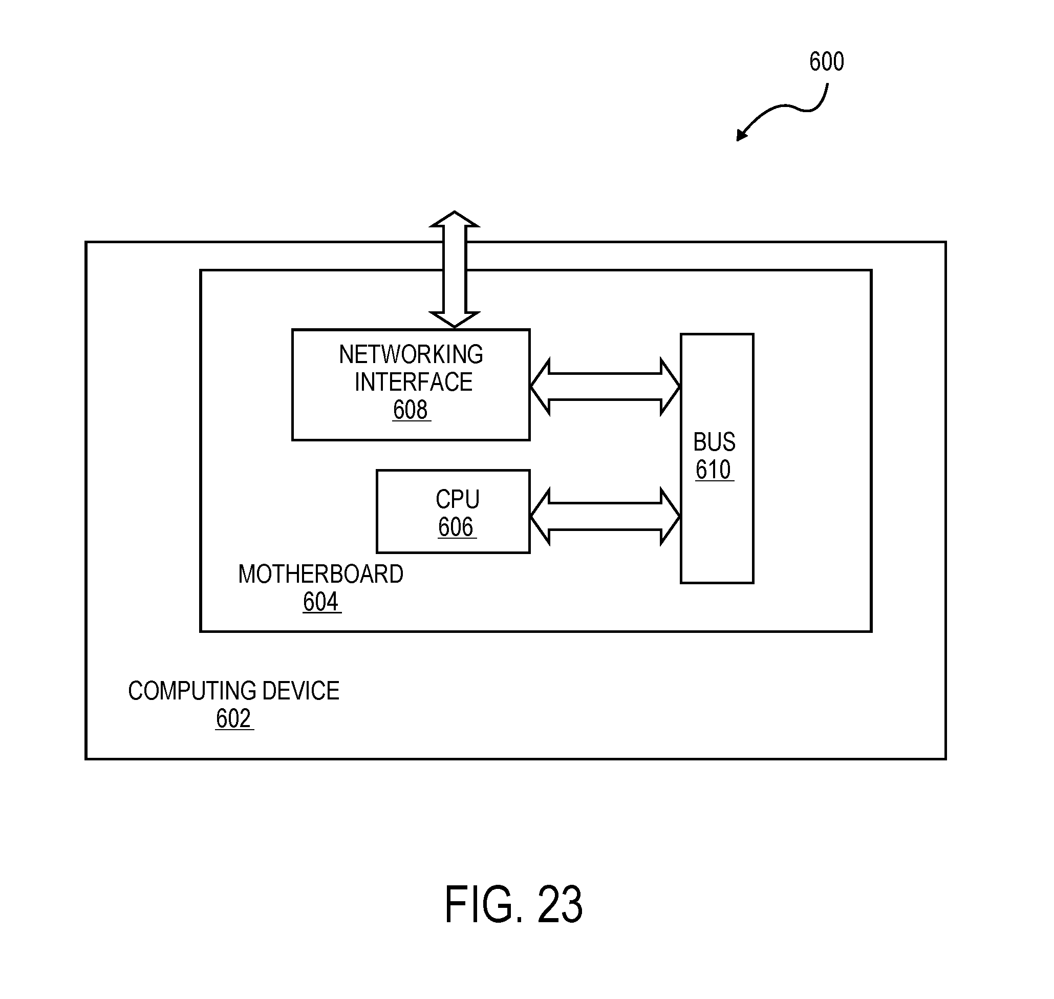
FIG. 23 is a block diagram, incorporating the above-illustrated thinned channel transistors in a system.
DETAILED DESCRIPTION
A process for fabricating CMOS field-effect transistors and the resultant transistors are described. In the following description, numerous specific details are set forth, such as specific dimensions and chemical regimes, in order to provide a thorough understanding of the present invention. It will be apparent to one skilled in the art that the present invention may be practiced without these specific details. In other instances, well-known processing steps, such as cleaning steps, are not described in detail, in order to not unnecessarily obscure the present invention.
A problem associated with small body devices is illustrated in FIG. 1A. A tri-gate structure 10 is shown traversing a silicon body at the channel region 14 of a transistor. The semiconductor body or fin has been thinned at the gate edges 11. This thinning is the result of processing used for defining the body, forming spacers, and cleaning of oxides. This processing can so reduce the body such that it may no longer have sufficient silicon seed to support the growth of an epitaxial layer. Often, as much as 20-50% of the body at the edge of the gate can be lost during such processing. In addition to yield loss, this results in higher source/drain resistance and the consequential reduction in transistor performance.
A similar problem is shown in FIG. 1B, where the n type or intrinsic channel region 15 is formed between the relatively thin regions 16 of the source and drain extension regions of a depletion mode planar transistor. Thus, the problem of thinning at the gate edges is not limited to tri-gate structures, or for that matter, SOI substrates, but can also occur in a bulk silicon layer or a delta-doped transistor, as shown in FIG. 1B. In the structure of FIG. 1B, an epitaxial layer is grown on a heavily doped substrate 14. An etchant discriminates between the epitaxially grown layer and the substrate 14, allowing the channel region 15 to be defined. The source and drain regions 17 are grown following the etching of the region 15. The structure is described in the application referenced in the Prior Art and Related Art section of this application.
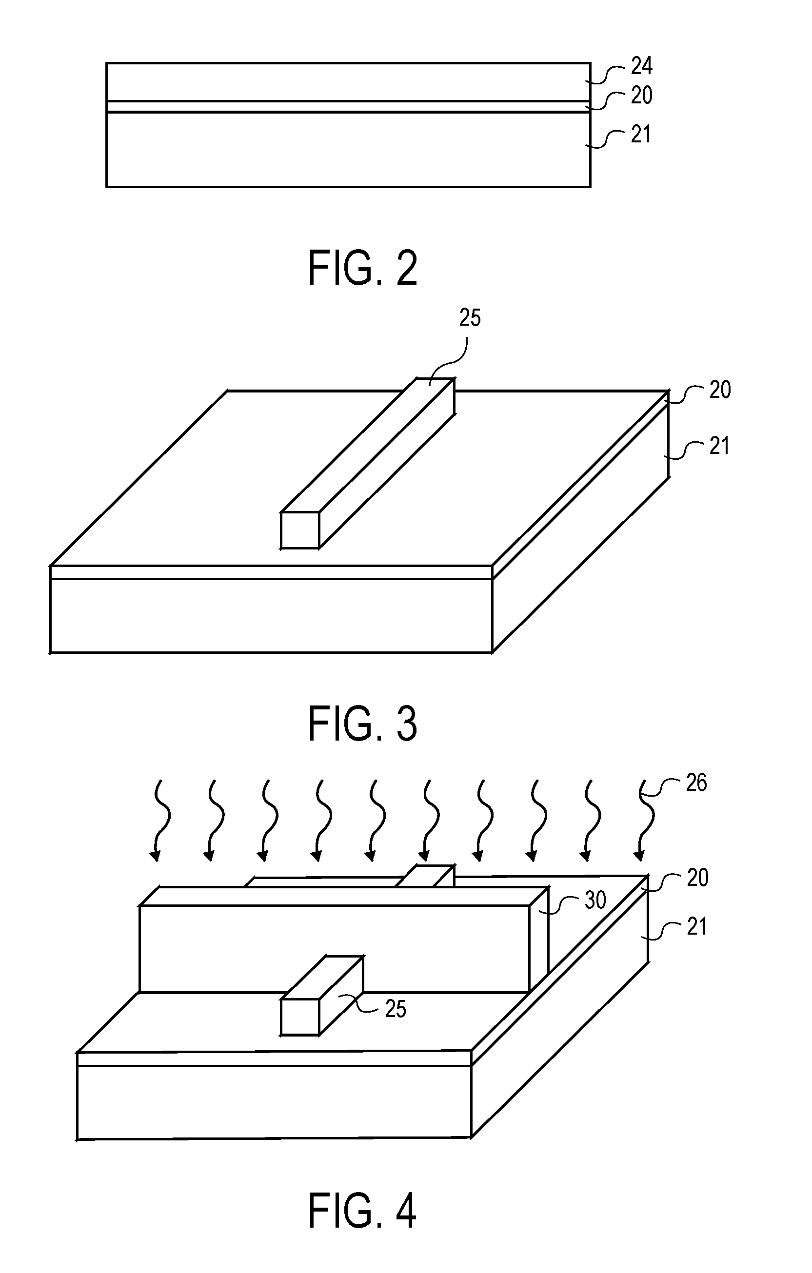
In a first embodiment, transistors are fabricated on an oxide layer 20 which is disposed on a silicon substrate 21 shown in FIG. 2. The transistor bodies are fabricated from a monocrystalline, silicon layer 24 disposed on the oxide layer 20. This SOI substrate is well-known in the semiconductor industry. By way of example, the SOI substrate is fabricated by bonding the oxide layer 20 and silicon layer 24 onto the substrate 21, and then planarizing the layer 24 so that it is relatively thin. Other techniques are known for forming an SOI substrate including, for instance, the implantation of oxygen into the silicon substrate to form a buried oxide layer. Other semiconductor materials, other than silicon, may also be used such as gallium arsenide.
The layer 24 may be selectively ion implanted with a p type dopant in regions where n channel transistors are to be fabricated, and with a n type dopant in those regions where p channel devices are to be fabricated. This is used to provide the relatively light doping typically found in the channel regions of MOS devices fabricated in a CMOS integrated circuit.
In the description below, for the first embodiment, the fabrication of a single n channel transistor is described. As will be appreciated in the typical integrated circuit, both n and p channel devices are fabricated. Also, in the processing for the first embodiment, a protective oxide (not shown) is disposed on the silicon layer 24 followed by the deposition of a silicon nitride layer. The nitride layer acts as a hard mask to define silicon bodies such as the silicon body 25 of FIG. 3.
Assume for a particular process that the silicon body, in the channel region of a field-effect transistor, should ideally have a height of 20 nm and a width of 20 nm. Using the prior art processing associated with the transistor of FIG. 1, the thickness of the silicon layer from which the body is etched would also have a thickness of 20 nm. As will be seen for the embodiment of FIGS. 2-11, the layer 24 may initially be thicker than 20 nm, and will subsequently be thinned in the channel region. This thinning only occurs in the channel region, leaving the source and drain regions thicker, thereby reducing the external resistance. This will become more apparent in the description below.
A polysilicon layer is formed over the structure of FIG. 3 and etched to define a dummy gate 30 which extends over the body 25 as seen in FIG. 4. (A dummy gate oxide which subsequently acts as an etch stop is not shown.) The region of the body 25 below the dummy gate 30, as will be seen, is the channel region for this replacement gate process. Once the dummy gate 30 has been defined, phosphorous or arsenic may be implanted into the body 25 in alignment with the dummy gate, as illustrated by the ion implantation 26. This ion implantation defines the tip or extension source and drain regions frequently used in CMOS transistors.
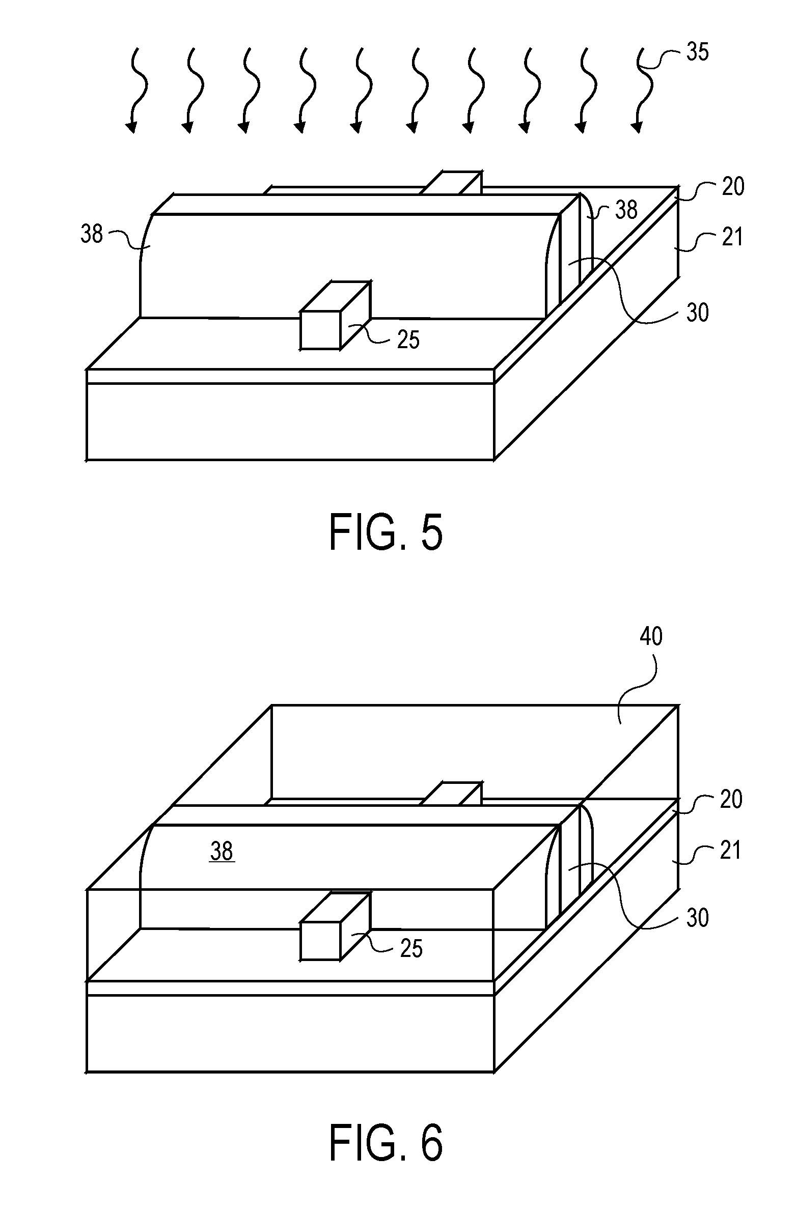
Next, a layer of silicon nitride is conformally deposited over the structure of FIG. 4, and is used to fabricate the spacers 38 shown in FIG. 5. Ordinary, well-known, anisotropic etching may be used to fabricate the spacers. In one embodiment, a carbon-doped nitride, doped with 5-13% carbon concentration is used for the spacers. As will be discussed later, prior to the formation of the nitride layer, an oxide layer present on the body 25 is removed. This cleaning process is one of the processes that typically reduces the thickness of the body at the edges of the gate. After the spacer formation, the main part of the source and drain regions are formed through ion implantation 35 shown in FIG. 5. For the n channel device, arsenic or phosphorous is used with an implant dose of up to 1.times.10.sup.19-1.times.10.sup.20 atoms/cm.sup.3.
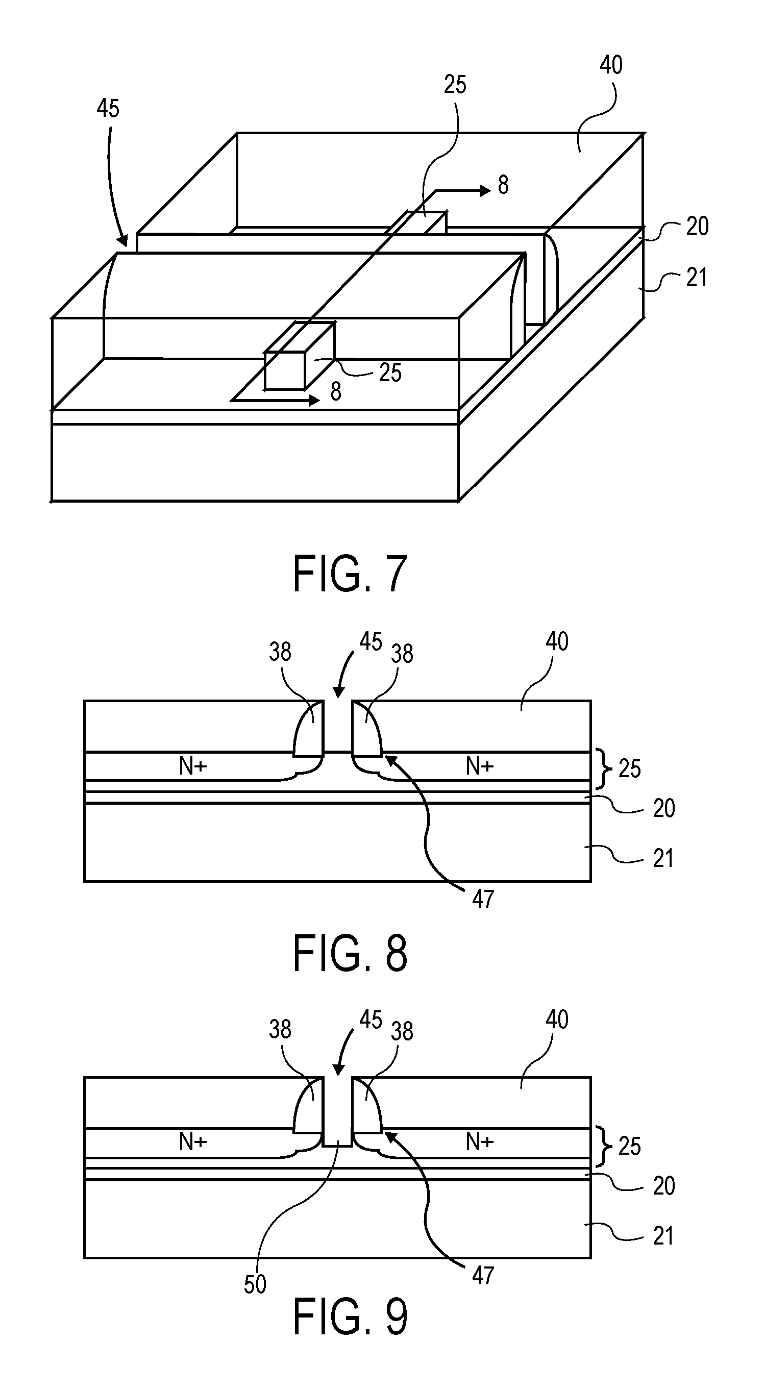
A dielectric layer 40 is now conformally deposited over the structure of FIG. 5, as shown in FIG. 6. This may comprise a silicon dioxide layer which will become an interlayer dielectric (ILD) in an integrated circuit. A low-k dielectric or a sacrificial dielectric layer may be used. In any event, the layer 40 typically has the mechanical strength to withstand a planarization process such as chemical mechanical polishing (CMP).
After the deposition and planarization of the dielectric layer 40, a wet etch is used to remove the dummy polysilicon gate 30, leaving the opening 45, as shown in FIG. 7. (The dummy gate oxide (not shown) is also removed.) The cross-sectional view of FIG. 8 taken through section line 8-8 of FIG. 7, better shows the opening 45. Also better shown in FIG. 8, is that the spacers 38 are recessed at 47 into the body 25. As mentioned earlier, after the source and drain tip implant and before the spacer material is deposited, an oxide layer is removed from the body 25. This results in the loss of some of the body material and, in part, accounts for the thinning occurring in the prior art structure shown at 11 of FIG. 1A. The removal of this oxide is important in some processes, as will be discussed later.
Following the removal of the dummy gate, any oxide over the body 25 within the opening 45 is removed in an ordinary cleaning step. Then, the structure of FIG. 8 is placed in a selective silicon bath such as NH.sub.4OH which reduces the size of the body within the opening 45. This etching reduces both the height of the body as seen at 50 of FIG. 9, as well as the width of the body. This allows the channel region of the body 25 to be thinned to a target height and thickness. Again, assume that the target height and thickness of the body 25 in the channel region is 20.times.20 nm. A thicker and wider body 25 may be initially formed since it is thinned in this etching step. Importantly, this etching step does not thin the body 25 outside of the channel region. Consequently, if the body 25 is initially thicker and wider, the source and drain regions remain thicker or wider after the channel region has been thinned. Thus, by starting with a thicker and wider body, there is more silicon left after the cleaning process, and the severe thinning shown at 11 of FIG. 1A is avoided.
Next, a gate dielectric 60 is formed on exposed surfaces which includes the sides and top of the body 25 lying within the opening 45. The layer 60 also deposits on the interior sidewalls of the spacers 38 and on the upper surface of the dielectric layer 40. The gate dielectric, in one embodiment, has a high dielectric constant (k), such as a metal oxide dielectric, for instance, HfO.sub.2 or ZrO.sub.2 or other high k dielectrics, such as PZT or BST. The gate dielectric may be formed by any well-known technique such as atomic layer deposition (ALD) or chemical vapor deposition (CVD). Alternately, the gate dielectric may be a grown dielectric. For instance, the gate dielectric 60, may be a silicon dioxide film grown with a wet or dry oxidation process to a thickness between 5-50 .ANG..
Following this, also as seen in FIG. 10, a gate electrode (metal) layer 61 is formed over the gate dielectric layer 60. The gate electrode layer 61 may be formed by blanket deposition of a suitable gate electrode material. In one embodiment, a gate electrode material comprises a metal film such as tungsten, tantalum, titanium and/or nitrides and alloys thereof. For the n channel transistors, a work function in the range of 3.9 to 4.6 eV may be used. For the p channel transistors, a work function of 4.6 to 5.2 eV may be used. Accordingly, for substrates with both n channel and p channel transistors, two separate metal deposition processes may need to be used.
The metal layer 61 is planarized using, for example CMP, and the planarization continues until at least the upper surface of the dielectric layer 40 is exposed, as shown in FIG. 11.
Standard processing is now used to complete the transistor of FIG. 11.
Alternate processing is next described in conjunction with FIGS. 12-14. The numbering used in FIG. 12 includes a "0" after the numbers used in FIGS. 2-11 for corresponding layers and members. For instance, the spacers 38 of FIG. 11 are shown as spacers 380 in FIG. 12. In FIG. 12, a substrate 210, insulator 200 and body 250 are seen along with the source and drain regions.
The processing leading up to FIG. 12 is the same as the processing as in the prior embodiment, with one exception. This difference is that the hard mask defining the bodies or fins, such as body 250, is not immediately removed after defining the bodies. Rather, the polysilicon dummy gate structure is formed over the hard mask. Then, where the body is not protected by the polysilicon dummy gate, the hard mask is removed. Consequently, the hard mask 260 remains over the channel region, and after the spacers are formed and dummy gate removed, the hard mask 260 is exposed in opening 450 of FIG. 12.
The structure of FIG. 12 is again illustrated in FIG. 13 from the view taken through the lines 13-13 of FIG. 12. In this view, the silicon body 250 and mask 260 are shown with the spacer 380 in the background. The dimension 280 of FIG. 13 is the width of the body 250 in the channel region.
Wet etching is now used to etch the silicon body 250 with, for example, NH.sub.4OH. This thins the width of the silicon body without changing its height, as shown in FIG. 14. Note, in FIG. 14 the remaining body 250 is narrower than its original dimension 280, while its height has not changed. For some semiconductor processes, better control may be obtained when only the width of the silicon body is etched. Thus, only the width of the body in the channel region is reduced to a predetermined target dimension, without reducing the height or width of the source and drain regions as this occurs.
After this etching step, the hard mask 260 is removed, then the high k dielectric and metal gates are formed, as was the case in the previous embodiment.
As mentioned earlier, the silicon dioxide layer, which typically is present on the silicon body, is removed before the deposition of the spacer material. This was discussed in conjunction with the recess 47 of FIG. 8. This is done because an undesirable reaction may occur between the oxide layer and the high k dielectric, if a high temperature anneal is used to activate the doping in the source and drain regions after the replacement gate is formed. At least the sides of the oxide layer, if not removed, may contact the high k dielectric and cause this problem. This is not a problem, however, if the annealing of the source and drain regions occurs before the high k dielectric is formed.
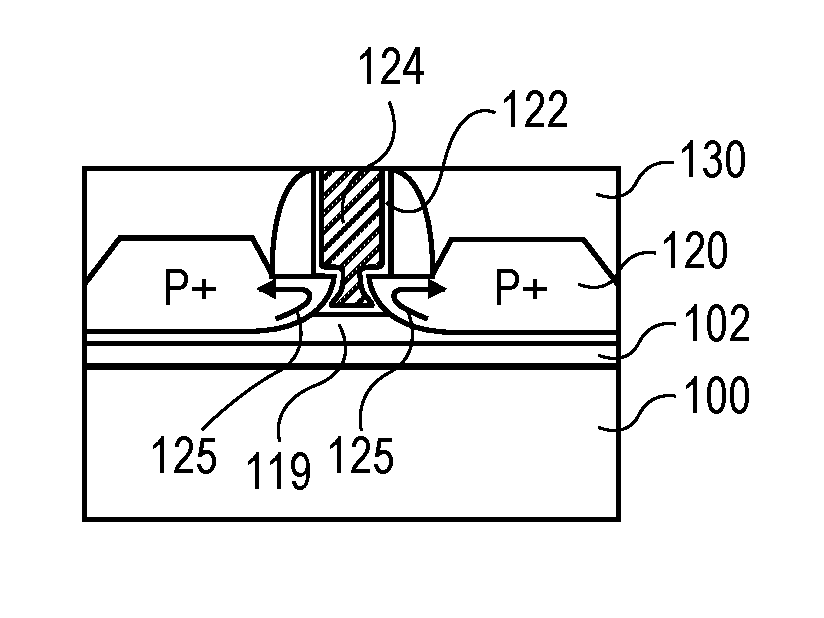
The thinning of the channel region described above can also be used on a planar, bulk transistor or a transistor formed in a delta-doped substrate. FIGS. 15-21 below describe the formation of a depletion mode transistor with raised source and drain regions, where controlled thinning of the channel region occurs.
FIG. 15 illustrates an SOI substrate having a base 100, oxide layer 102 and a monocrystalline silicon layer 103. For the depletion mode transistor, the layer 103, or at least the region where the depletion mode transistor is fabricated, is lightly doped with an n type dopant or is intrinsic silicon, or other semiconductor material. A gate structure is fabricated on a dummy gate oxide layer 110. This structure comprises a polysilicon dummy gate 104 and spacers 105.
Following this, as shown in FIG. 16, the semiconductor layer 103 is etched isotropically in alignment with the gate structure. This etching undercuts the gate structure as illustrated at undercut 114. The remaining silicon from layer 103, is the channel region 119, seen in FIG. 16.
Raised source and drain regions are then epitaxially grown to establish a shallow, highly doped source/drain tip (extension) that laterally extends the distance under the gate edge to the channel region 119. Separate processing is used for the p-channel and n-channel transistors with each of the source and drain regions being grown in different processing, both with in-situ doping. This results in the source and drain regions being highly doped, in one case with a p-type dopant, and in the other case with an n-type dopant.
In forming a PMOS transistor, the source and drain regions are raised as illustrated. They may be formed by selectively depositing epitaxial boron (B) doped silicon or SiGe with germanium concentrations up to 30%, as an example. Under the processing conditions of 100 sccm of dichlorosilane (DCS), 20 slm H.sub.2, 750-800.degree. C., 20 Torr, 150-200 sccm HCl, a diborane (B.sub.2H.sub.6) flow of 150-200 sccm and a GeH.sub.4 flow of 150-200 sccm, a highly doped SiGe film with a deposition rate of 20 nm/min, B concentration of 1E20 cm.sup.-3 and a germanium concentration of 20% is achieved. A low resistivity of 0.7-0.9 mOhm-cm resulting from the high B concentration in the film provides the benefit of high conductivity in the tip source/drain regions and thereby reduced R.sub.external. SiGe in the source/drain regions exerts compressive strain on the channel, which in turn results in enhanced mobility and improved transistor performance.
For an NMOS transistor, the source/drain regions are formed, for instance, using in-situ phosphorous doped silicon deposited selectively under processing conditions of 100 sccm of DCS, 25-50 sccm HCl, 200-300 sccm of 1% PH.sub.3 with a carrier H.sub.2 gas flow of 20 slm at 750.degree. C. and 20 Torr. A phosphorous concentration of 2E20 cm.sup.-3 with a resistivity of 0.4-0.6 mOhm-cm is achieved in the deposited film.
The resultant structure is shown in FIG. 17. Ion implantation of boron may be used to more heavily dope the source and drain region beyond the edges of the gate structure shown in FIG. 17.
A dielectric layer 130 is now formed over the structure of FIG. 17. This corresponds to the dielectric layers 40 and 400 in the prior embodiments. Again, this layer may be an ILD layer or a sacrificial layer. An etchant is used to etch away the dummy gate, providing an opening 140 seen in FIG. 18. This exposes the underlying oxide layer 110. The oxide layer 110 is removed with an ordinary etchant as shown in FIG. 19, thereby exposing the channel region 119.
Now, the channel region can be etched to reduce its cross section as shown in FIG. 20. A tetramethylammonium hydroxide (TMAH) or ammonium hydroxide solution with an appropriate pH value is used to selectively etch the exposed n type or intrinsic silicon channel region 119 without affecting the p+ source and drain regions. This etchant is highly selective, and thus leaves in place the tips 150 of the source and drain regions 120 while the thinning of the channel region 119 occurs. The boron-doped silicon has a sufficiently different lattice energy than the phosphorous- or arsenic-doped silicon, thereby allowing this selective etching to occur. In one process, this etching is done at a megasonic energy level of between 600 and 1100 kHz. The tips 150 shown in FIG. 20, thus remain even though the channel region falls below the raised source and drain regions.
A high k dielectric gate layer 122 may next be conformally deposited using, for instance, ALD. Following this, metal gate layer 124 is formed. The appropriate work function for the layer 124 is used as discussed above for the layer 61.
The structure of FIG. 21 is planarized with, for instance, CMP to provide the structure of FIG. 22. In the finished device, the final recessed channel 119 thus has raised, source/drain extension regions. This allows the current from the channel inversion layer to spread upward into these extension regions as shown by the lines 125. In contrast in examining FIG. 1B at 16, the current can only spread outward and downward, thereby resulting in higher series resistance.
The transistor fabricated as described above may be incorporated into an integrated circuit, central processing unit, which in turn is part of a computing device or system. FIG. 23 illustrates such a system 600 in accordance with one embodiment. As illustrated, for the embodiment, system 600 includes computing device 602 for processing data. Computing device 602 may include a motherboard 604. Motherboard 604 may include in particular a processor 606, and a networking interface 608 coupled to a bus 610. More specifically, processor 606 may comprise the transistors of FIG. 11 or 22, as examples, of the above-described transistor.
Depending on the applications, system 600 may include other components, including but are not limited to, volatile and non-volatile memory, a graphics processor, a digital signal processor, a crypto processor, a chipset, mass storage (such as hard disk, compact disk (CD), digital versatile disk (DVD) and so forth), and so forth.
In various embodiments, system 600 may be a personal digital assistant (PDA), a mobile phone, a tablet computing device, a laptop computing device, a desktop computing device, a set-top box, an entertainment control unit, a digital camera, a digital video recorder, a CD player, a DVD player, or other digital device of the like.
Thus, improved processing has been described that allows a channel region to be controllably thinned, and that permits the source/drain regions to have less resistance.
* * * * *
D00000
D00001
D00002
D00003
D00004
D00005
D00006
D00007
D00008
D00009
XML
uspto.report is an independent third-party trademark research tool that is not affiliated, endorsed, or sponsored by the United States Patent and Trademark Office (USPTO) or any other governmental organization. The information provided by uspto.report is based on publicly available data at the time of writing and is intended for informational purposes only.
While we strive to provide accurate and up-to-date information, we do not guarantee the accuracy, completeness, reliability, or suitability of the information displayed on this site. The use of this site is at your own risk. Any reliance you place on such information is therefore strictly at your own risk.
All official trademark data, including owner information, should be verified by visiting the official USPTO website at www.uspto.gov. This site is not intended to replace professional legal advice and should not be used as a substitute for consulting with a legal professional who is knowledgeable about trademark law.