Semiconductor device
Yokoyama , et al. Sept
U.S. patent number D859,334 [Application Number D/643,229] was granted by the patent office on 2019-09-10 for semiconductor device. This patent grant is currently assigned to Mitsubishi Electric Corporation. The grantee listed for this patent is Mitsubishi Electric Corporation. Invention is credited to Maki Hasegawa, Shigeru Mori, Shuhei Yokoyama.


| United States Patent | D859,334 |
| Yokoyama , et al. | September 10, 2019 |
Semiconductor device
Claims
CLAIM The ornamental design for a semiconductor device, as shown and described.
| Inventors: | Yokoyama; Shuhei (Tokyo, JP), Hasegawa; Maki (Tokyo, JP), Mori; Shigeru (Tokyo, JP) | ||||||||||
|---|---|---|---|---|---|---|---|---|---|---|---|
| Applicant: |
|
||||||||||
| Assignee: | Mitsubishi Electric Corporation
(Tokyo, JP) |
||||||||||
| Appl. No.: | D/643,229 | ||||||||||
| Filed: | April 5, 2018 |
Foreign Application Priority Data
| Oct 26, 2017 [JP] | 2017-023790 | |||
| Oct 26, 2017 [JP] | 2017-023791 | |||
| Current U.S. Class: | D13/182 |
| Current International Class: | 1303 |
| Field of Search: | ;D13/182 |
References Cited [Referenced By]
U.S. Patent Documents
| 3602846 | August 1971 | Hauser |
| 3762039 | October 1973 | Douglass |
| D259560 | June 1981 | Mochizuki |
| D259782 | July 1981 | Mochizuki |
| D259783 | July 1981 | Mochizuki |
| D260091 | August 1981 | Mochizuki |
| 4663833 | May 1987 | Tanaka |
| D345731 | April 1994 | Owens |
| D357901 | May 1995 | Horman |
| D358806 | May 1995 | Siegel |
| D359028 | June 1995 | Siegel |
| 5557504 | September 1996 | Siegel |
| D394244 | May 1998 | Majumdar |
| D396211 | July 1998 | Enomoto |
| D396212 | July 1998 | Enomoto |
| D396213 | July 1998 | Enomoto |
| D396847 | August 1998 | Nakayama |
| 5798570 | August 1998 | Watanabe |
| D421421 | March 2000 | Kashio |
| D427977 | July 2000 | Takizawa |
| 6093957 | July 2000 | Kwon |
| D432097 | October 2000 | Song |
| 6238953 | May 2001 | Tanaka |
| D448739 | October 2001 | Iwasaki |
| D466485 | December 2002 | Maehara |
| D466873 | December 2002 | Kasem |
| D472528 | April 2003 | Kasem |
| D473199 | April 2003 | Sako |
| 6555899 | April 2003 | Chung |
| D476962 | July 2003 | Yoshihira |
| D480371 | October 2003 | Sako |
| 6992386 | January 2006 | Hata |
| D539761 | April 2007 | Takahashi |
| D548202 | August 2007 | Takahashi |
| D548203 | August 2007 | Takahashi |
| D717253 | November 2014 | Jo |
| D717254 | November 2014 | Jo |
| D717255 | November 2014 | Lim |
| D717256 | November 2014 | Sohn |
| D719113 | December 2014 | Sohn |
| D770994 | November 2016 | Hasegawa |
| D783550 | April 2017 | Hasegawa |
| D824866 | August 2018 | Matsubara |
Attorney, Agent or Firm: Studebaker & Brackett PC
Description
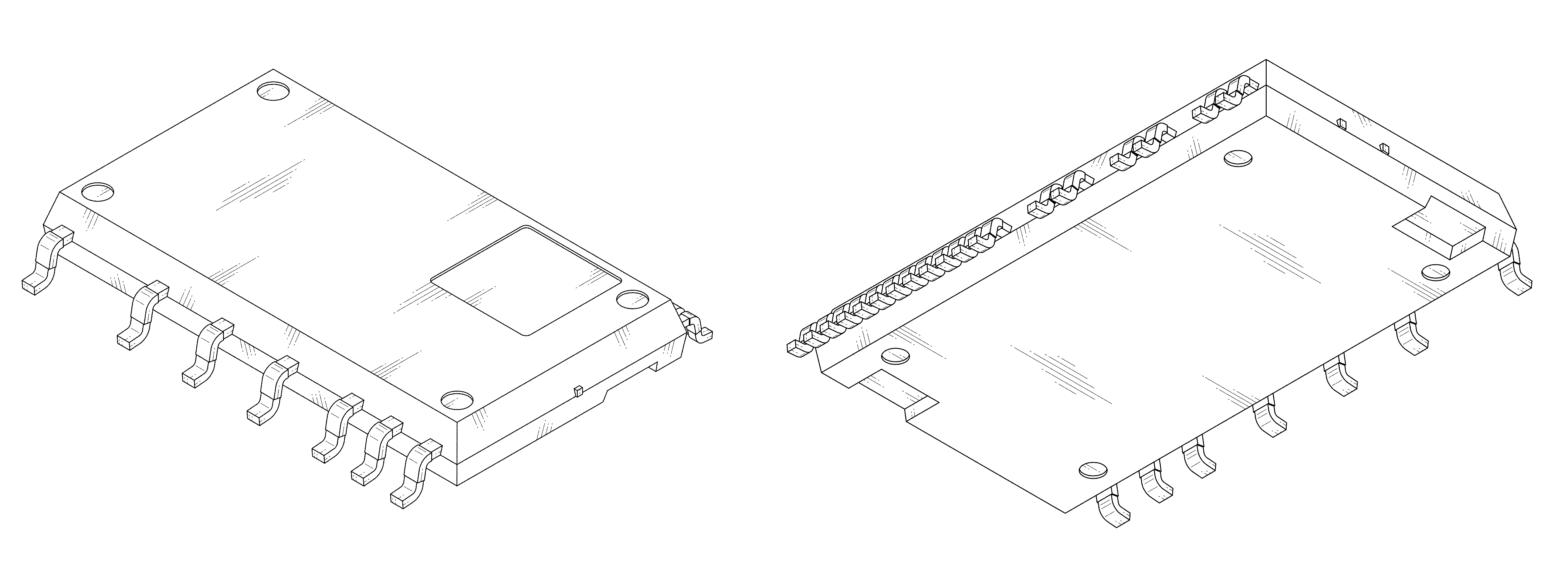
FIG. 1 is a front, bottom and right side perspective view of a semiconductor device showing our new design;
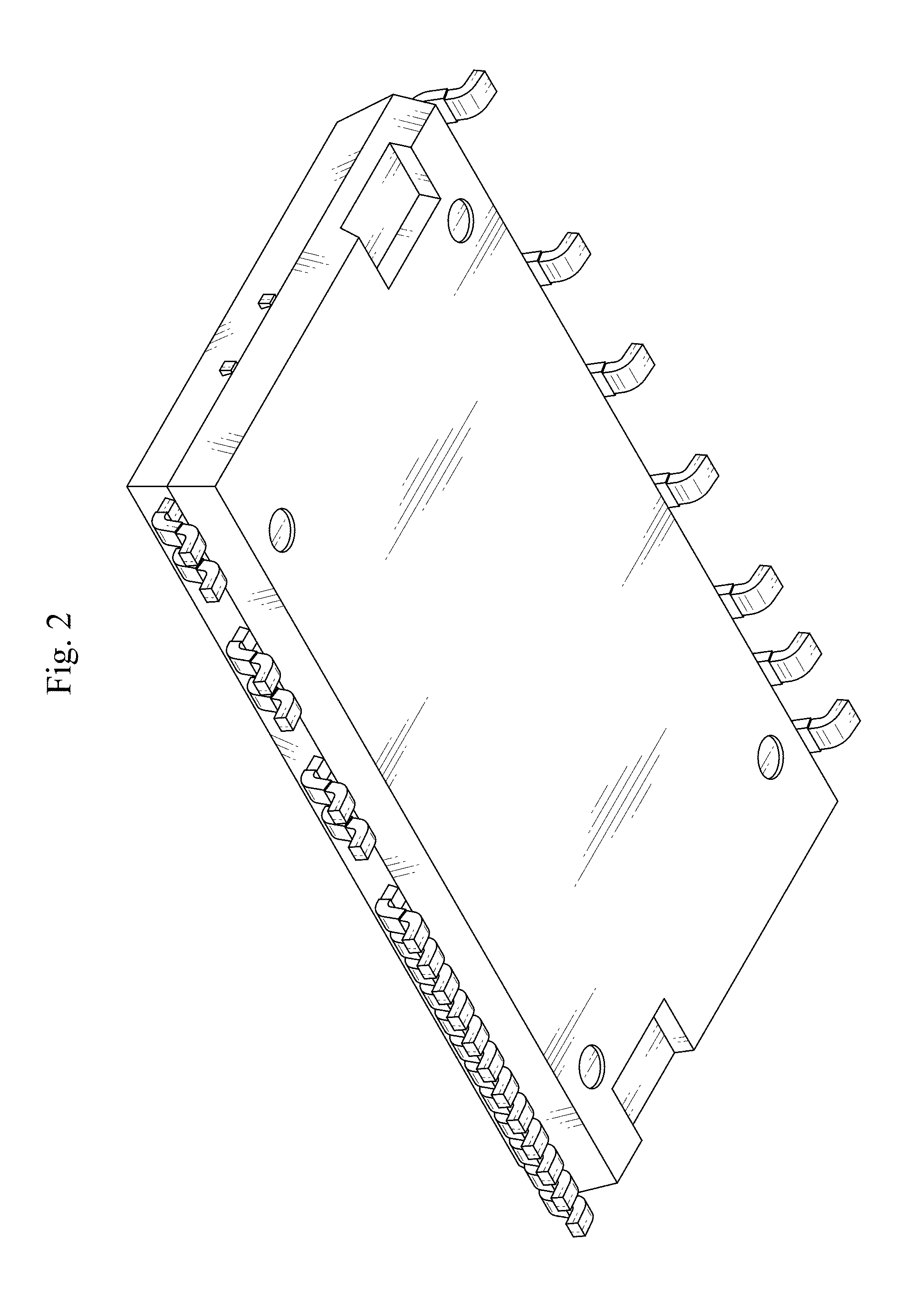
FIG. 2 is a rear, top and left side perspective view thereof;
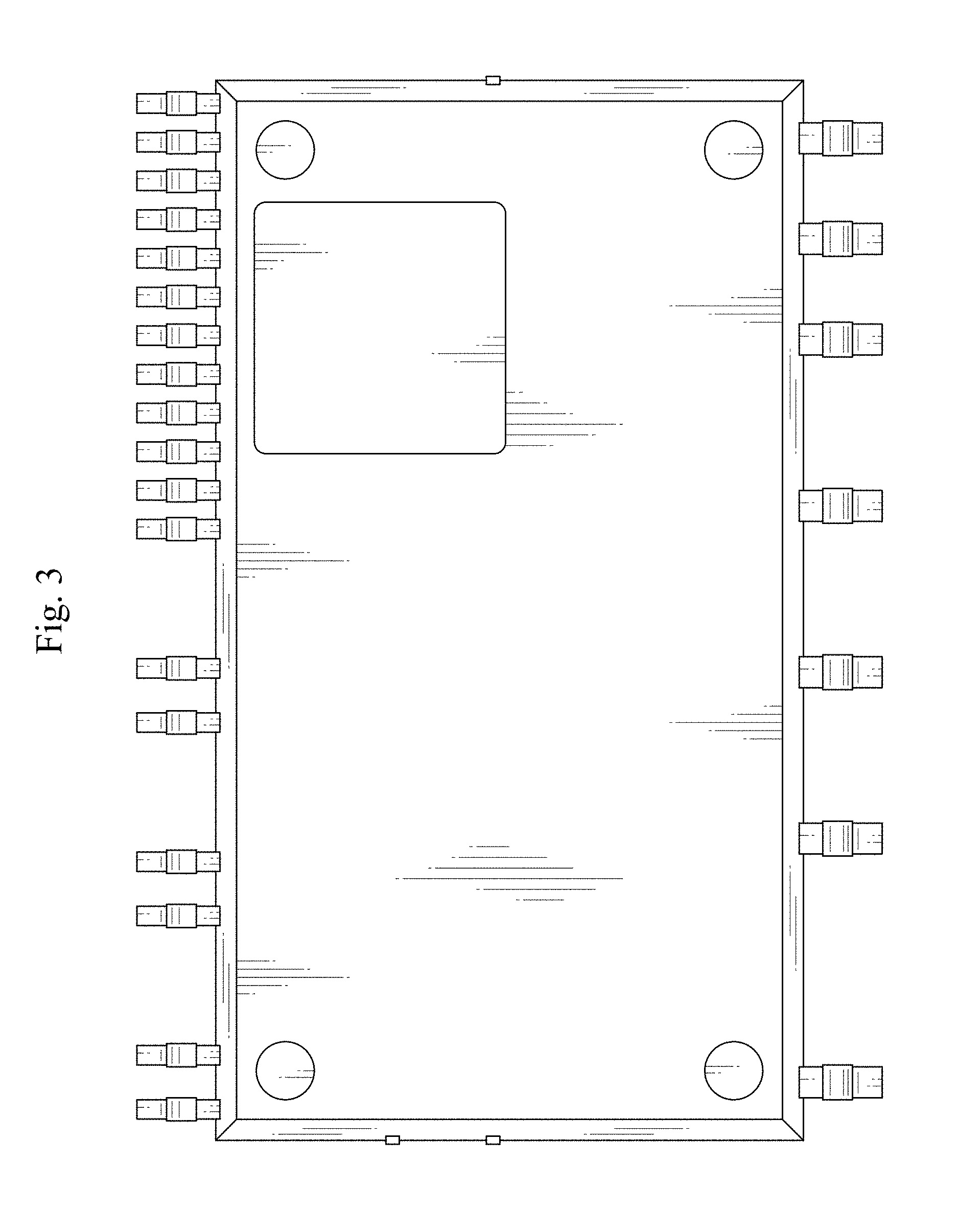
FIG. 3 is a front view thereof;
FIG. 4 is a rear view thereof;
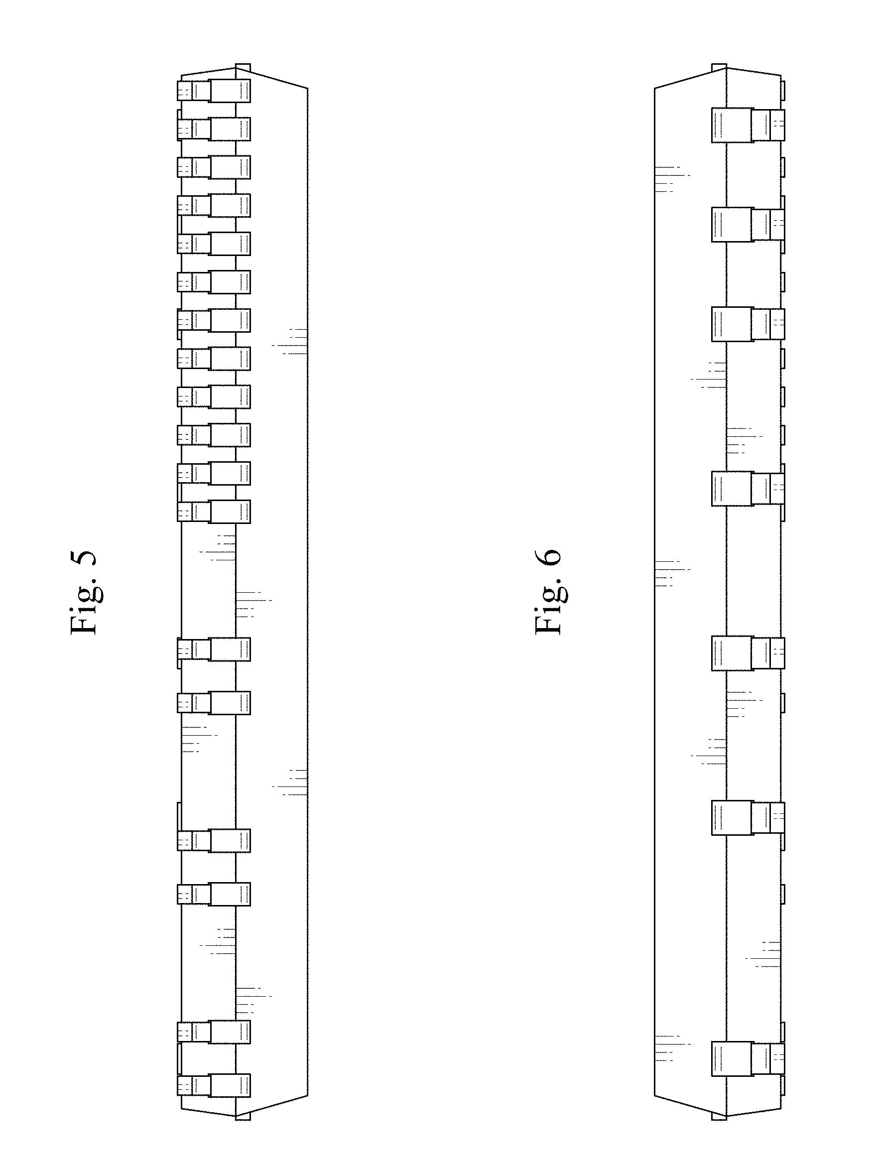
FIG. 5 is a top view thereof;
FIG. 6 is a bottom view thereof;
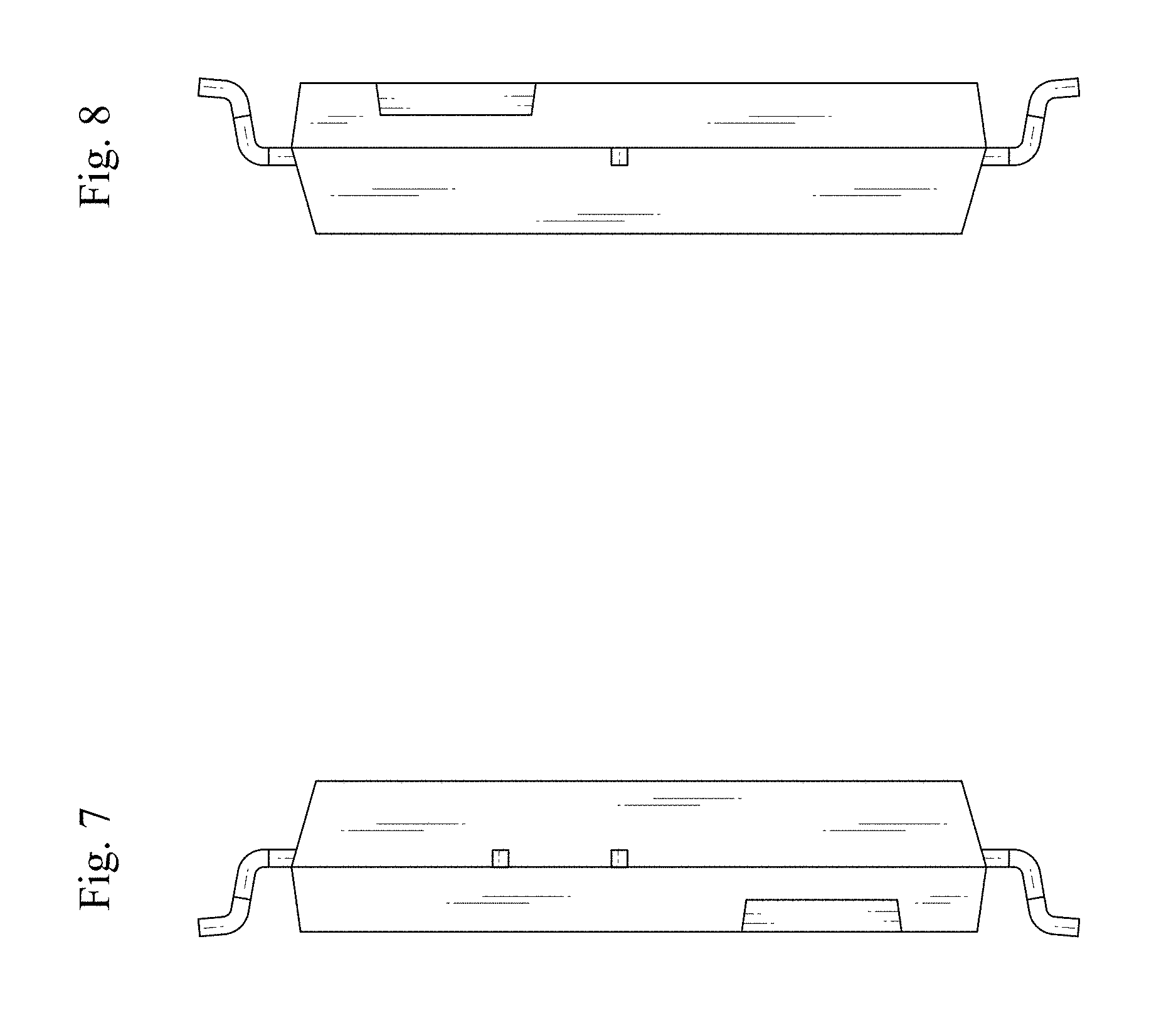
FIG. 7 is a left side view thereof; and,
FIG. 8 is a right side view thereof.
* * * * *
D00000
D00001
D00002
D00003
D00004
D00005
D00006
XML
uspto.report is an independent third-party trademark research tool that is not affiliated, endorsed, or sponsored by the United States Patent and Trademark Office (USPTO) or any other governmental organization. The information provided by uspto.report is based on publicly available data at the time of writing and is intended for informational purposes only.
While we strive to provide accurate and up-to-date information, we do not guarantee the accuracy, completeness, reliability, or suitability of the information displayed on this site. The use of this site is at your own risk. Any reliance you place on such information is therefore strictly at your own risk.
All official trademark data, including owner information, should be verified by visiting the official USPTO website at www.uspto.gov. This site is not intended to replace professional legal advice and should not be used as a substitute for consulting with a legal professional who is knowledgeable about trademark law.