Apparatus and method for deposition and etch in gap fill
Singhal , et al. March 23, 2
U.S. patent number 10,957,514 [Application Number 16/453,237] was granted by the patent office on 2021-03-23 for apparatus and method for deposition and etch in gap fill. This patent grant is currently assigned to Lam Research Corporation. The grantee listed for this patent is Lam Research Corporation. Invention is credited to Martin E. Freeborn, Akhil Singhal, Patrick A. van Cleemput, Bart J. van Schravendijk.


View All Diagrams
| United States Patent | 10,957,514 |
| Singhal , et al. | March 23, 2021 |
Apparatus and method for deposition and etch in gap fill
Abstract
Provided are apparatuses and methods for performing deposition and etch processes in an integrated tool. An apparatus may include a plasma processing chamber that is a capacitively-coupled plasma reactor, and the plasma processing chamber can include a showerhead that includes a top electrode and a pedestal that includes a bottom electrode. The apparatus may be configured with an RF hardware configuration so that an RF generator may power the top electrode in a deposition mode and power the bottom electrode in an etch mode. In some implementations, the apparatus can include one or more switches so that at least an HFRF generator is electrically connected to the showerhead in a deposition mode, and the HFRF generator and an LFRF generator is electrically connected to the pedestal and the showerhead is grounded in the etch mode.
| Inventors: | Singhal; Akhil (Portland, OR), van Cleemput; Patrick A. (West Linn, OR), Freeborn; Martin E. (San Jose, CA), van Schravendijk; Bart J. (Palo Alto, CA) | ||||||||||
|---|---|---|---|---|---|---|---|---|---|---|---|
| Applicant: |
|
||||||||||
| Assignee: | Lam Research Corporation
(Fremont, CA) |
||||||||||
| Family ID: | 1000005441237 | ||||||||||
| Appl. No.: | 16/453,237 | ||||||||||
| Filed: | June 26, 2019 |
Prior Publication Data
| Document Identifier | Publication Date | |
|---|---|---|
| US 20190385820 A1 | Dec 19, 2019 | |
Related U.S. Patent Documents
| Application Number | Filing Date | Patent Number | Issue Date | ||
|---|---|---|---|---|---|
| 15683397 | Aug 22, 2017 | 10373806 | |||
| 15199608 | Sep 26, 2017 | 9773643 | |||
| Current U.S. Class: | 1/1 |
| Current CPC Class: | C23C 16/45544 (20130101); C23C 16/045 (20130101); C23C 16/50 (20130101); H01J 37/32091 (20130101); C23C 16/45565 (20130101); H01J 37/32577 (20130101); H01J 37/3244 (20130101); H01J 37/32568 (20130101); C23C 16/45536 (20130101); H01J 37/32174 (20130101); H01J 37/32715 (20130101); H01J 37/32449 (20130101); C23C 16/5096 (20130101); C23C 16/4554 (20130101); H01J 2237/3321 (20130101); H01J 2237/334 (20130101) |
| Current International Class: | H01J 37/32 (20060101); C23C 16/509 (20060101); C23C 16/455 (20060101); C23C 16/04 (20060101); C23C 16/50 (20060101) |
References Cited [Referenced By]
U.S. Patent Documents
| 4500563 | February 1985 | Ellenberger et al. |
| 5094984 | March 1992 | Liu et al. |
| 5223443 | June 1993 | Chinn et al. |
| 5318928 | June 1994 | Gegenwart et al. |
| 5496608 | March 1996 | Matsuda et al. |
| 5593914 | January 1997 | Evans, Jr. et al. |
| 5670432 | September 1997 | Tsai |
| 5856003 | January 1999 | Chiu |
| 5874368 | February 1999 | Laxman et al. |
| 5916365 | June 1999 | Sherman |
| 5932286 | August 1999 | Beinglass et al. |
| 6069058 | May 2000 | Hong |
| 6100202 | August 2000 | Lin et al. |
| 6156149 | December 2000 | Cheung et al. |
| 6218293 | April 2001 | Kraus et al. |
| 6270572 | August 2001 | Kim et al. |
| 6346741 | February 2002 | Van Buskirk et al. |
| 6391803 | May 2002 | Kim et al. |
| 6399221 | June 2002 | Marks et al. |
| 6416822 | July 2002 | Chiang et al. |
| 6428859 | August 2002 | Chiang et al. |
| 6465272 | October 2002 | Davis, Jr. et al. |
| 6468924 | October 2002 | Lee et al. |
| 6482726 | November 2002 | Aminpur et al. |
| 6509601 | January 2003 | Lee et al. |
| 6528430 | March 2003 | Kwan et al. |
| 6551893 | April 2003 | Zheng et al. |
| 6569501 | May 2003 | Chiang et al. |
| 6576053 | June 2003 | Kim et al. |
| 6602784 | August 2003 | Sneh |
| 6632478 | October 2003 | Gaillard et al. |
| 6645574 | November 2003 | Lee et al. |
| 6689220 | February 2004 | Nguyen |
| 6723595 | April 2004 | Park |
| 6730614 | May 2004 | Lim et al. |
| 6743738 | June 2004 | Todd |
| 6756318 | June 2004 | Nguyen et al. |
| 6765303 | July 2004 | Krivokapic et al. |
| 6809421 | October 2004 | Hayasaka et al. |
| 6828218 | December 2004 | Kim et al. |
| 6835417 | December 2004 | Saenger et al. |
| 6861356 | March 2005 | Matsuse et al. |
| 6884466 | April 2005 | Kaloyeros et al. |
| 6930058 | August 2005 | Hill et al. |
| 6930060 | August 2005 | Chou et al. |
| 6943092 | September 2005 | Kim et al. |
| 6962876 | November 2005 | Ahn et al. |
| 6987240 | January 2006 | Jennings et al. |
| 7001844 | February 2006 | Chakravarti et al. |
| 7041335 | May 2006 | Chung |
| 7077904 | July 2006 | Cho et al. |
| 7081271 | July 2006 | Chung et al. |
| 7097886 | August 2006 | Moghadam et al. |
| 7109129 | September 2006 | Papasouliotis |
| 7115166 | October 2006 | Vaartstra et al. |
| 7115528 | October 2006 | Vaartstra et al. |
| 7122222 | October 2006 | Xiao et al. |
| 7122464 | October 2006 | Vaarstra |
| 7125815 | October 2006 | Vaartstra |
| 7132353 | November 2006 | Xia et al. |
| 7141278 | November 2006 | Koh et al. |
| 7148155 | December 2006 | Tarafdar et al. |
| 7151039 | December 2006 | Lee et al. |
| 7172792 | February 2007 | Wang et al. |
| 7176084 | February 2007 | Lee et al. |
| 7205187 | April 2007 | Leith et al. |
| 7223649 | May 2007 | Oh et al. |
| 7235484 | June 2007 | Nguyen et al. |
| 7241686 | July 2007 | Marcadal et al. |
| 7244668 | July 2007 | Kim |
| 7250083 | July 2007 | Sneh |
| 7259050 | August 2007 | Chen et al. |
| 7261919 | August 2007 | Mehregany et al. |
| 7294582 | November 2007 | Haverkort et al. |
| 7297641 | November 2007 | Todd et al. |
| 7300885 | November 2007 | Hasebe et al. |
| 7314835 | January 2008 | Ishizaka et al. |
| 7341959 | March 2008 | Brcka |
| 7351668 | April 2008 | Chou et al. |
| 7361538 | April 2008 | Luan et al. |
| 7361611 | April 2008 | Chakravarti et al. |
| 7390743 | June 2008 | Shin |
| 7393561 | July 2008 | Paranjpe |
| 7399388 | July 2008 | Moghadam et al. |
| 7419888 | September 2008 | Yang et al. |
| 7435454 | October 2008 | Brcka |
| 7435684 | October 2008 | Lang et al. |
| 7462571 | December 2008 | Hasebe et al. |
| 7482247 | January 2009 | Papasouliotis et al. |
| 7488694 | February 2009 | Kim et al. |
| 7507676 | March 2009 | Chou et al. |
| 7510984 | March 2009 | Saito et al. |
| 7521331 | April 2009 | Park et al. |
| 7524762 | April 2009 | Marcadal et al. |
| 7544615 | June 2009 | Vaartstra |
| 7572052 | August 2009 | Ravi et al. |
| 7592231 | September 2009 | Cheng et al. |
| 7595010 | September 2009 | Chakravarti et al. |
| 7601648 | October 2009 | Chua et al. |
| 7615438 | November 2009 | Ahn et al. |
| 7615449 | November 2009 | Chung et al. |
| 7622369 | November 2009 | Lee et al. |
| 7622383 | November 2009 | Kim et al. |
| 7629267 | December 2009 | Wan et al. |
| 7632757 | December 2009 | Matsuura |
| 7633125 | December 2009 | Lu et al. |
| 7638170 | December 2009 | Li |
| 7645484 | January 2010 | Ishizaka |
| 7651729 | January 2010 | Kim et al. |
| 7651730 | January 2010 | Hasebe |
| 7651953 | January 2010 | Todd et al. |
| 7651959 | January 2010 | Fukazawa et al. |
| 7682657 | March 2010 | Sherman |
| 7687409 | March 2010 | Ahn et al. |
| 7713592 | May 2010 | Nguyen et al. |
| 7745346 | June 2010 | Hausmann et al. |
| 7758920 | July 2010 | Hasebe et al. |
| 7776733 | August 2010 | Hasegawa |
| 7790633 | September 2010 | Tarafdar et al. |
| 7825039 | November 2010 | Takahashi et al. |
| 7863190 | January 2011 | Papasouliotis et al. |
| 7906168 | March 2011 | Hasebe et al. |
| 7919416 | April 2011 | Lee et al. |
| 7923068 | April 2011 | Dickey et al. |
| 7923378 | April 2011 | Hasebe et al. |
| 7959985 | June 2011 | Ishizaka et al. |
| 7964241 | June 2011 | Hasebe et al. |
| 7964513 | June 2011 | Todd et al. |
| 7972980 | July 2011 | Lee et al. |
| 7981473 | July 2011 | Kim et al. |
| 7989365 | August 2011 | Park et al. |
| 8034673 | October 2011 | Kadonaga et al. |
| 8080290 | December 2011 | Hasebe et al. |
| 8101531 | January 2012 | Li et al. |
| 8119424 | February 2012 | Mather et al. |
| 8119544 | February 2012 | Hasebe et al. |
| 8133797 | March 2012 | van Schravendijk et al. |
| 8178448 | May 2012 | Nodera et al. |
| 8227032 | July 2012 | Dussarrat et al. |
| 8257789 | September 2012 | Matsunaga et al. |
| 8278224 | October 2012 | Mui et al. |
| 8334218 | December 2012 | Van Nooten et al. |
| 8338312 | December 2012 | Sato et al. |
| 8357619 | January 2013 | Hasebe et al. |
| 8366953 | February 2013 | Kohno et al. |
| 8383525 | February 2013 | Raisanen et al. |
| 8394466 | March 2013 | Hong et al. |
| 8524612 | September 2013 | Li et al. |
| 8592328 | November 2013 | Hausmann et al. |
| 8633050 | January 2014 | Pierreux |
| 8637411 | January 2014 | Swaminathan et al. |
| 8647993 | February 2014 | Lavoie et al. |
| 8669185 | March 2014 | Onizawa et al. |
| 8728955 | May 2014 | LaVoie et al. |
| 8728956 | May 2014 | LaVoie et al. |
| 8846484 | September 2014 | Lee et al. |
| 8956983 | February 2015 | Swaminathan et al. |
| 8999859 | April 2015 | Swaminathan et al. |
| 9023693 | May 2015 | Lin et al. |
| 9076646 | July 2015 | Sims et al. |
| 9214334 | December 2015 | Swaminathan et al. |
| 9230800 | January 2016 | Lavoie et al. |
| 9257274 | February 2016 | Kang et al. |
| 9287113 | March 2016 | Kang et al. |
| 9355839 | May 2016 | Swaminathan et al. |
| 9355886 | May 2016 | Swaminathan et al. |
| 9373500 | June 2016 | Swaminathan et al. |
| 9406693 | August 2016 | Pang et al. |
| 9502238 | November 2016 | Danek et al. |
| 9564312 | February 2017 | Henri et al. |
| 9570274 | February 2017 | Swaminathan et al. |
| 9570290 | February 2017 | Swaminathan et al. |
| 9611544 | April 2017 | Lavoie et al. |
| 9627221 | April 2017 | Zaitsu |
| 9673041 | June 2017 | Swaminathan et al. |
| 9685320 | June 2017 | Kang et al. |
| 9773643 | September 2017 | Singhal |
| 9786570 | October 2017 | Kang et al. |
| 9793110 | October 2017 | Kang et al. |
| 9875891 | January 2018 | Henri et al. |
| 9892917 | February 2018 | Swaminathan et al. |
| 9997357 | June 2018 | Arghavani et al. |
| 10008428 | June 2018 | Kang et al. |
| 10037884 | July 2018 | Ou et al. |
| 10043655 | August 2018 | Swaminathan et al. |
| 10043657 | August 2018 | Swaminathan et al. |
| 10062563 | August 2018 | Kumar et al. |
| 10269559 | April 2019 | Abel et al. |
| 10361076 | July 2019 | Kang et al. |
| 10373806 | August 2019 | Singhal et al. |
| 10559468 | February 2020 | Arghavani et al. |
| 10804099 | October 2020 | Henri et al. |
| 2002/0066411 | June 2002 | Chiang et al. |
| 2002/0076507 | June 2002 | Chiang et al. |
| 2002/0153101 | October 2002 | Nguyen et al. |
| 2002/0175393 | November 2002 | Baum et al. |
| 2003/0008070 | January 2003 | Seutter et al. |
| 2003/0024477 | February 2003 | Okuda et al. |
| 2003/0143839 | July 2003 | Raaijmakers et al. |
| 2003/0200917 | October 2003 | Vaartstra |
| 2003/0216006 | November 2003 | Li et al. |
| 2004/0033698 | February 2004 | Lee et al. |
| 2004/0043633 | March 2004 | Vaartstra |
| 2004/0053515 | March 2004 | Comita et al. |
| 2004/0121164 | June 2004 | Iacovangelo et al. |
| 2004/0129212 | July 2004 | Gadgil et al. |
| 2004/0146644 | July 2004 | Xiao et al. |
| 2004/0157472 | August 2004 | Sugino et al. |
| 2004/0171280 | September 2004 | Conley, Jr. et al. |
| 2004/0219746 | November 2004 | Vaartstra et al. |
| 2004/0219784 | November 2004 | Kang et al. |
| 2004/0231799 | November 2004 | Lee et al. |
| 2005/0005851 | January 2005 | Keshner et al. |
| 2005/0009368 | January 2005 | Vaartsra |
| 2005/0042865 | February 2005 | Cabral et al. |
| 2005/0079661 | April 2005 | Cho et al. |
| 2005/0100670 | May 2005 | Dussarrat et al. |
| 2005/0109276 | May 2005 | Iyer et al. |
| 2005/0118837 | June 2005 | Todd et al. |
| 2005/0142795 | June 2005 | Ahn et al. |
| 2005/0158983 | July 2005 | Hoshi et al. |
| 2005/0159017 | July 2005 | Kim et al. |
| 2005/0181535 | August 2005 | Yun et al. |
| 2005/0184397 | August 2005 | Gates et al. |
| 2005/0196977 | September 2005 | Saito et al. |
| 2005/0208718 | September 2005 | Lim et al. |
| 2005/0230047 | October 2005 | Collins et al. |
| 2005/0233553 | October 2005 | Kountz et al. |
| 2005/0260347 | November 2005 | Narwankar et al. |
| 2005/0276099 | December 2005 | Horng et al. |
| 2005/0276930 | December 2005 | Gates et al. |
| 2005/0282346 | December 2005 | Barth et al. |
| 2005/0287775 | December 2005 | Hasebe et al. |
| 2006/0003557 | January 2006 | Cabral et al. |
| 2006/0009041 | January 2006 | Iyer et al. |
| 2006/0030148 | February 2006 | Seutter et al. |
| 2006/0032442 | February 2006 | Hasebe |
| 2006/0032443 | February 2006 | Hasebe et al. |
| 2006/0084283 | April 2006 | Paranjpe et al. |
| 2006/0088985 | April 2006 | Haverkort et al. |
| 2006/0105106 | May 2006 | Balseanu et al. |
| 2006/0165890 | July 2006 | Kaushal et al. |
| 2006/0183055 | August 2006 | O'Neill et al. |
| 2006/0199357 | September 2006 | Wan et al. |
| 2006/0216418 | September 2006 | Matsuura |
| 2006/0228868 | October 2006 | Ahn et al. |
| 2006/0286774 | December 2006 | Singh et al. |
| 2006/0286776 | December 2006 | Ranish et al. |
| 2006/0286818 | December 2006 | Wang et al. |
| 2007/0010071 | January 2007 | Matsuura |
| 2007/0026540 | February 2007 | Nooten et al. |
| 2007/0032047 | February 2007 | Hasebe et al. |
| 2007/0048455 | March 2007 | Koh et al. |
| 2007/0065576 | March 2007 | Singh et al. |
| 2007/0087574 | April 2007 | Gupta et al. |
| 2007/0087581 | April 2007 | Singh et al. |
| 2007/0116887 | May 2007 | Faguet |
| 2007/0119370 | May 2007 | Ma et al. |
| 2007/0134942 | June 2007 | Ahn et al. |
| 2007/0137572 | June 2007 | Matsuura et al. |
| 2007/0145483 | June 2007 | Ono |
| 2007/0167028 | July 2007 | Chou et al. |
| 2007/0215036 | September 2007 | Park et al. |
| 2007/0218701 | September 2007 | Shimizu et al. |
| 2007/0231487 | October 2007 | Ishizaka |
| 2007/0232082 | October 2007 | Balseanu et al. |
| 2007/0243693 | October 2007 | Nemani et al. |
| 2007/0245959 | October 2007 | Paterson |
| 2007/0251444 | November 2007 | Gros-Jean et al. |
| 2007/0259110 | November 2007 | Mahajani et al. |
| 2007/0281495 | December 2007 | Mallick et al. |
| 2007/0298585 | December 2007 | Lubomirsky et al. |
| 2008/0014759 | January 2008 | Chua et al. |
| 2008/0038936 | February 2008 | Todd et al. |
| 2008/0063791 | March 2008 | Hasebe et al. |
| 2008/0075881 | March 2008 | Won et al. |
| 2008/0081470 | April 2008 | Clark |
| 2008/0085610 | April 2008 | Wang et al. |
| 2008/0087890 | April 2008 | Ahn et al. |
| 2008/0123394 | May 2008 | Lee et al. |
| 2008/0131601 | June 2008 | Kim et al. |
| 2008/0138996 | June 2008 | Nishizuka |
| 2008/0139003 | June 2008 | Pirzada et al. |
| 2008/0207007 | August 2008 | Thridandam et al. |
| 2008/0213479 | September 2008 | Chou et al. |
| 2008/0233762 | September 2008 | Hong |
| 2008/0242116 | October 2008 | Clark |
| 2008/0260969 | October 2008 | Dussarrat et al. |
| 2008/0274302 | November 2008 | Hasebe et al. |
| 2008/0311760 | December 2008 | Nodera et al. |
| 2008/0317972 | December 2008 | Hendriks et al. |
| 2009/0018668 | January 2009 | Galbraith |
| 2009/0039349 | February 2009 | Honda |
| 2009/0041952 | February 2009 | Yoon et al. |
| 2009/0065896 | March 2009 | Hwang et al. |
| 2009/0075490 | March 2009 | Dussarrat |
| 2009/0148625 | June 2009 | Yeom et al. |
| 2009/0155606 | June 2009 | Yoon et al. |
| 2009/0155968 | June 2009 | Min et al. |
| 2009/0163012 | June 2009 | Clark et al. |
| 2009/0191687 | July 2009 | Hong et al. |
| 2009/0191722 | July 2009 | Hasebe et al. |
| 2009/0203197 | August 2009 | Hanawa et al. |
| 2009/0208880 | August 2009 | Nemani et al. |
| 2009/0278224 | November 2009 | Kim et al. |
| 2009/0286381 | November 2009 | van Schravendijk et al. |
| 2010/0022099 | January 2010 | Van Nooten et al. |
| 2010/0025824 | February 2010 | Chen et al. |
| 2010/0048011 | February 2010 | Yeh et al. |
| 2010/0051578 | March 2010 | Chang et al. |
| 2010/0051579 | March 2010 | Kobayashi |
| 2010/0078316 | April 2010 | Edakawa et al. |
| 2010/0096687 | April 2010 | Balseanu et al. |
| 2010/0096688 | April 2010 | Balseanu et al. |
| 2010/0099236 | April 2010 | Kwon et al. |
| 2010/0099271 | April 2010 | Hausmann et al. |
| 2010/0102417 | April 2010 | Ganguli et al. |
| 2010/0120262 | May 2010 | Vorsa et al. |
| 2010/0124618 | May 2010 | Kobayashi et al. |
| 2010/0124621 | May 2010 | Kobayashi et al. |
| 2010/0136260 | June 2010 | Matsunaga et al. |
| 2010/0136313 | June 2010 | Shimizu et al. |
| 2010/0144162 | June 2010 | Lee et al. |
| 2010/0167555 | July 2010 | Maula et al. |
| 2010/0190353 | July 2010 | Nguyen et al. |
| 2010/0197129 | August 2010 | Ishikawa |
| 2010/0216268 | August 2010 | Katayama et al. |
| 2010/0221925 | September 2010 | Lee et al. |
| 2010/0244114 | September 2010 | Konno et al. |
| 2010/0255218 | October 2010 | Oka et al. |
| 2010/0304574 | December 2010 | Nodera et al. |
| 2010/0310791 | December 2010 | Shimazu et al. |
| 2011/0003445 | January 2011 | Murata et al. |
| 2011/0014795 | January 2011 | Lee et al. |
| 2011/0014796 | January 2011 | Hayashi |
| 2011/0014798 | January 2011 | Mallick et al. |
| 2011/0042744 | February 2011 | Cheng et al. |
| 2011/0064969 | March 2011 | Chen et al. |
| 2011/0086516 | April 2011 | Lee et al. |
| 2011/0121354 | May 2011 | Schmid et al. |
| 2011/0124187 | May 2011 | Afzali-Ardakani et al. |
| 2011/0139176 | June 2011 | Cheung et al. |
| 2011/0143548 | June 2011 | Cheung et al. |
| 2011/0151142 | June 2011 | Seamons et al. |
| 2011/0151246 | June 2011 | Ramon Moreno et al. |
| 2011/0151674 | June 2011 | Tang et al. |
| 2011/0151678 | June 2011 | Ashtiani et al. |
| 2011/0159202 | June 2011 | Matsushita et al. |
| 2011/0171775 | July 2011 | Yamamoto et al. |
| 2011/0176967 | July 2011 | Okuda et al. |
| 2011/0198756 | August 2011 | Thenappan et al. |
| 2011/0201210 | August 2011 | Sato et al. |
| 2011/0215445 | September 2011 | Yang et al. |
| 2011/0256726 | October 2011 | LaVoie et al. |
| 2011/0256734 | October 2011 | Hausmann et al. |
| 2011/0298099 | December 2011 | Lee et al. |
| 2011/0309475 | December 2011 | Lee |
| 2012/0009802 | January 2012 | LaVoie et al. |
| 2012/0009803 | January 2012 | Jung et al. |
| 2012/0021252 | January 2012 | Lee |
| 2012/0028454 | February 2012 | Swaminathan et al. |
| 2012/0028469 | February 2012 | Onizawa et al. |
| 2012/0058282 | March 2012 | Hong et al. |
| 2012/0064682 | March 2012 | Jang et al. |
| 2012/0074844 | March 2012 | York et al. |
| 2012/0077349 | March 2012 | Li et al. |
| 2012/0086048 | April 2012 | Park et al. |
| 2012/0108079 | May 2012 | Mahajani |
| 2012/0113672 | May 2012 | Dubrow et al. |
| 2012/0164846 | June 2012 | Ha et al. |
| 2012/0193693 | August 2012 | Kanaya |
| 2012/0213940 | August 2012 | Mallick |
| 2012/0280200 | November 2012 | Tada et al. |
| 2012/0282418 | November 2012 | Chou et al. |
| 2012/0315394 | December 2012 | Ito |
| 2013/0040447 | February 2013 | Swaminathan et al. |
| 2013/0043512 | February 2013 | Huang et al. |
| 2013/0058161 | March 2013 | Yamanaka et al. |
| 2013/0058162 | March 2013 | Yamanaka et al. |
| 2013/0065404 | March 2013 | Weidman et al. |
| 2013/0071580 | March 2013 | Weidman et al. |
| 2013/0084688 | April 2013 | O'Meara et al. |
| 2013/0113073 | May 2013 | Liu et al. |
| 2013/0115783 | May 2013 | Kim et al. |
| 2013/0189854 | July 2013 | Hausmann et al. |
| 2013/0196516 | August 2013 | Lavoie et al. |
| 2013/0252437 | September 2013 | Sano et al. |
| 2013/0309415 | November 2013 | Swaminathan et al. |
| 2013/0319329 | December 2013 | Li et al. |
| 2013/0323923 | December 2013 | Koehler et al. |
| 2013/0344248 | December 2013 | Clark |
| 2014/0030444 | January 2014 | Swaminathan et al. |
| 2014/0051262 | February 2014 | Lavoie et al. |
| 2014/0087066 | March 2014 | Wang et al. |
| 2014/0106574 | April 2014 | Kang |
| 2014/0113457 | April 2014 | Sims et al. |
| 2014/0120270 | May 2014 | Tour et al. |
| 2014/0120737 | May 2014 | Swaminathan et al. |
| 2014/0134827 | May 2014 | Swaminathan et al. |
| 2014/0141542 | May 2014 | Kang et al. |
| 2014/0141626 | May 2014 | Hausmann et al. |
| 2014/0170853 | June 2014 | Shamma et al. |
| 2014/0182619 | July 2014 | Goto et al. |
| 2014/0209562 | July 2014 | LaVoie et al. |
| 2014/0216337 | August 2014 | Swaminathan et al. |
| 2014/0239462 | August 2014 | Shamma et al. |
| 2014/0262038 | September 2014 | Wang et al. |
| 2014/0264555 | September 2014 | Ahn et al. |
| 2014/0273428 | September 2014 | Shero et al. |
| 2014/0273528 | September 2014 | Niskanen et al. |
| 2014/0295084 | October 2014 | Shirai et al. |
| 2014/0302686 | October 2014 | Pan et al. |
| 2015/0041867 | February 2015 | Han |
| 2015/0048740 | February 2015 | Valcore, Jr. et al. |
| 2015/0093902 | April 2015 | Huang et al. |
| 2015/0109814 | April 2015 | Chen et al. |
| 2015/0126042 | May 2015 | Pasquale et al. |
| 2015/0147483 | May 2015 | Fukazawa |
| 2015/0159271 | June 2015 | Lee et al. |
| 2015/0170900 | June 2015 | LaVoie |
| 2015/0206719 | July 2015 | Swaminathan et al. |
| 2015/0235835 | August 2015 | Swaminathan et al. |
| 2015/0243883 | August 2015 | Swaminathan et al. |
| 2015/0249013 | September 2015 | Arghavani et al. |
| 2015/0294905 | October 2015 | Wu et al. |
| 2016/0020092 | January 2016 | Kang et al. |
| 2016/0064211 | March 2016 | Swaminathan et al. |
| 2016/0079037 | March 2016 | Hirano et al. |
| 2016/0118246 | April 2016 | Kang et al. |
| 2016/0148800 | May 2016 | Henri et al. |
| 2016/0148806 | May 2016 | Henri et al. |
| 2016/0155676 | June 2016 | Kang et al. |
| 2016/0163539 | June 2016 | Kang et al. |
| 2016/0163972 | June 2016 | Swaminathan et al. |
| 2016/0240428 | August 2016 | Tung et al. |
| 2016/0251756 | September 2016 | Lansalot-Matras et al. |
| 2016/0260584 | September 2016 | Marakhtanov |
| 2016/0293385 | October 2016 | Kapoor et al. |
| 2016/0293398 | October 2016 | Danek et al. |
| 2016/0293838 | October 2016 | Swaminathan et al. |
| 2016/0322215 | November 2016 | Shaikh |
| 2016/0322371 | November 2016 | Yonemochi |
| 2016/0329206 | November 2016 | Kumar et al. |
| 2016/0329423 | November 2016 | Kawahara et al. |
| 2016/0336178 | November 2016 | Swaminathan et al. |
| 2016/0340782 | November 2016 | Chandrasekharan et al. |
| 2016/0365425 | December 2016 | Chen et al. |
| 2016/0379826 | December 2016 | Arghavani et al. |
| 2017/0009346 | January 2017 | Kumar et al. |
| 2017/0092735 | March 2017 | Hashemi et al. |
| 2017/0103891 | April 2017 | Lee et al. |
| 2017/0110364 | April 2017 | Song et al. |
| 2017/0110533 | April 2017 | Huang et al. |
| 2017/0117134 | April 2017 | Henri et al. |
| 2017/0117150 | April 2017 | Liao et al. |
| 2017/0140926 | May 2017 | Pore et al. |
| 2017/0148628 | May 2017 | Swaminathan et al. |
| 2017/0170026 | June 2017 | Hudson et al. |
| 2017/0226637 | August 2017 | Lubomirsky et al. |
| 2017/0263450 | September 2017 | Swaminathan et al. |
| 2017/0316988 | November 2017 | Kang et al. |
| 2017/0323786 | November 2017 | Kang et al. |
| 2018/0005801 | January 2018 | Singhal et al. |
| 2018/0005814 | January 2018 | Kumar et al. |
| 2018/0061628 | March 2018 | Ou et al. |
| 2018/0138028 | May 2018 | Henri et al. |
| 2018/0247875 | August 2018 | Kang et al. |
| 2018/0269061 | September 2018 | Arghavani et al. |
| 2018/0323057 | November 2018 | Kumar et al. |
| 2019/0080903 | March 2019 | Abel et al. |
| 2019/0311897 | October 2019 | Kang et al. |
| 2019/0385850 | December 2019 | Arghavani et al. |
| 1732288 | Feb 2006 | CN | |||
| 1841676 | Oct 2006 | CN | |||
| 1926668 | Mar 2007 | CN | |||
| 101006195 | Jul 2007 | CN | |||
| 101255548 | Sep 2008 | CN | |||
| 101328578 | Dec 2008 | CN | |||
| 101378007 | Mar 2009 | CN | |||
| 101416293 | Apr 2009 | CN | |||
| 101535524 | Sep 2009 | CN | |||
| 101736326 | Jun 2010 | CN | |||
| 101889331 | Nov 2010 | CN | |||
| 102005462 | Apr 2011 | CN | |||
| 102191479 | Sep 2011 | CN | |||
| 102471885 | May 2012 | CN | |||
| 102687249 | Sep 2012 | CN | |||
| 102906304 | Jan 2013 | CN | |||
| 103137864 | Jun 2013 | CN | |||
| 103928396 | Jul 2014 | CN | |||
| 105391427 | Mar 2016 | CN | |||
| 105719954 | Jun 2016 | CN | |||
| 0 277 766 | Aug 1988 | EP | |||
| 0 541 212 | May 1993 | EP | |||
| 1 081 754 | Jul 2001 | EP | |||
| 1 703 552 | Sep 2006 | EP | |||
| 2 278 046 | Jan 2011 | EP | |||
| S48-043472 | Jun 1973 | JP | |||
| H02-093071 | Apr 1990 | JP | |||
| H03-011635 | Jan 1991 | JP | |||
| 05-226279 | Sep 1993 | JP | |||
| H06-177120 | Jun 1994 | JP | |||
| H09-102494 | Apr 1997 | JP | |||
| H09-219401 | Aug 1997 | JP | |||
| 10-98032 | Apr 1998 | JP | |||
| H10-189467 | Jul 1998 | JP | |||
| H11-172439 | Jun 1999 | JP | |||
| 2001-274404 | Oct 2001 | JP | |||
| 2001-338922 | Dec 2001 | JP | |||
| 2002-009072 | Jan 2002 | JP | |||
| 2002-134497 | May 2002 | JP | |||
| 2002-164345 | Jun 2002 | JP | |||
| 2002-539640 | Nov 2002 | JP | |||
| 2005-210076 | Aug 2005 | JP | |||
| 2005-310927 | Nov 2005 | JP | |||
| 2006-060091 | Mar 2006 | JP | |||
| 2006-303431 | Nov 2006 | JP | |||
| 2007-165883 | Jun 2007 | JP | |||
| 2007-180362 | Jul 2007 | JP | |||
| 2007-189173 | Jul 2007 | JP | |||
| 2007-521658 | Aug 2007 | JP | |||
| 2007-287889 | Nov 2007 | JP | |||
| 2007-287890 | Nov 2007 | JP | |||
| 2008-500742 | Jan 2008 | JP | |||
| 2008-506262 | Feb 2008 | JP | |||
| 2008-060455 | Mar 2008 | JP | |||
| 2008-109093 | May 2008 | JP | |||
| 2008-517479 | May 2008 | JP | |||
| 2008-522405 | Jun 2008 | JP | |||
| 2008-182199 | Aug 2008 | JP | |||
| 2008-258591 | Oct 2008 | JP | |||
| 2008-294260 | Dec 2008 | JP | |||
| 2008-306093 | Dec 2008 | JP | |||
| 2009-65203 | Mar 2009 | JP | |||
| 2009-170823 | Jul 2009 | JP | |||
| 2009-540128 | Nov 2009 | JP | |||
| 4364320 | Nov 2009 | JP | |||
| 2010-10497 | Jan 2010 | JP | |||
| 2010-043081 | Feb 2010 | JP | |||
| 2010-103484 | May 2010 | JP | |||
| 2010-118664 | May 2010 | JP | |||
| 2010-152136 | Jul 2010 | JP | |||
| 2010-183069 | Aug 2010 | JP | |||
| 2010-530127 | Sep 2010 | JP | |||
| 2010-245518 | Oct 2010 | JP | |||
| 2010-251654 | Nov 2010 | JP | |||
| 2010-283388 | Dec 2010 | JP | |||
| 2010-539730 | Dec 2010 | JP | |||
| 2011-023576 | Feb 2011 | JP | |||
| 2011-023655 | Feb 2011 | JP | |||
| 2011-054968 | Mar 2011 | JP | |||
| 11-067744 | Apr 2011 | JP | |||
| 2011-187934 | Sep 2011 | JP | |||
| 2012-506640 | Mar 2012 | JP | |||
| 2012-199306 | Oct 2012 | JP | |||
| 2013-102130 | May 2013 | JP | |||
| 2013-166965 | Aug 2013 | JP | |||
| 2013-196822 | Sep 2013 | JP | |||
| 2013-225655 | Oct 2013 | JP | |||
| 2013-240042 | Nov 2013 | JP | |||
| 2014-532304 | Dec 2014 | JP | |||
| 10-2001-0111448 | Dec 2001 | KR | |||
| 10-0356473 | Oct 2002 | KR | |||
| 10-2004-0001036 | Jan 2004 | KR | |||
| 10-2006-0056883 | May 2006 | KR | |||
| 10-0721503 | May 2007 | KR | |||
| 10-2007-0060104 | Jun 2007 | KR | |||
| 10-0734748 | Jul 2007 | KR | |||
| 10-2009-0057665 | Jun 2009 | KR | |||
| 10-2009-0080019 | Jul 2009 | KR | |||
| 10-2009-0081396 | Jul 2009 | KR | |||
| 10-2009-0116433 | Nov 2009 | KR | |||
| 10-2010-0133377 | Dec 2010 | KR | |||
| 10-2011-0086090 | Jul 2011 | KR | |||
| 10-2013-0056608 | May 2013 | KR | |||
| 10-2015-0025224 | Mar 2015 | KR | |||
| 483103 | Apr 2002 | TW | |||
| 200701341 | Jan 2007 | TW | |||
| 2007/21306 | Jun 2007 | TW | |||
| 201009942 | Mar 2010 | TW | |||
| 201042706 | Dec 2010 | TW | |||
| 2011/13934 | Apr 2011 | TW | |||
| 201140695 | Nov 2011 | TW | |||
| 201144475 | Dec 2011 | TW | |||
| 201621974 | Jun 2016 | TW | |||
| WO 2004/032196 | Apr 2004 | WO | |||
| WO 2006/014471 | Feb 2006 | WO | |||
| WO 2006/018441 | Feb 2006 | WO | |||
| WO 2006/026350 | Mar 2006 | WO | |||
| WO 2006/104741 | Oct 2006 | WO | |||
| WO 2007/043709 | Apr 2007 | WO | |||
| WO 2007/118026 | Oct 2007 | WO | |||
| WO 2011/087580 | Jul 2011 | WO | |||
| WO 2011/087850 | Jul 2011 | WO | |||
| WO 2011/130326 | Oct 2011 | WO | |||
| WO 2011/130397 | Oct 2011 | WO | |||
| WO 2012/040317 | Mar 2012 | WO | |||
| WO 2012/048094 | Apr 2012 | WO | |||
| WO 2012/087737 | Jun 2012 | WO | |||
| WO 2013/032786 | Mar 2013 | WO | |||
| WO 2013/043330 | Mar 2013 | WO | |||
| WO 2013/065806 | May 2013 | WO | |||
| WO 2013/095396 | Jun 2013 | WO | |||
| WO 2013/112727 | Aug 2013 | WO | |||
Other References
|
US. Office Action dated Mar. 15, 2013 issued in U.S. Appl. No. 13/084,399. cited by applicant . U.S. Final Office Action dated Sep. 13, 2013 issued in U.S. Appl. No. 13/084,399. cited by applicant . U.S. Notice of Allowance dated Jan. 15, 2014 issued in U.S. Appl. No. 13/084,399. cited by applicant . U.S. Office Action dated Jan. 2, 2015 issued in U.S. Appl. No. 14/231,554. cited by applicant . U.S. Final Office Action dated Jun. 10, 2015 issued in U.S. Appl. No. 14/231,554. cited by applicant . U.S. Notice of Allowance dated Aug. 31, 2015 issued in U.S. Appl. No. 14/231,554. cited by applicant . U.S. Office Action dated Sep. 14, 2012 issued in U.S. Appl. No. 13/084,305. cited by applicant . U.S. Final Office Action dated Apr. 25, 2013 issued in U.S. Appl. No. 13/084,305. cited by applicant . U.S. Office Action dated Apr. 13, 2011 issued in U.S. Appl. No. 12/889,132. cited by applicant . U.S. Notice of Allowance dated Sep. 30, 2011 issued in U.S. Appl. No. 12/889,132. cited by applicant . U.S. Office Action dated Aug. 1, 2012 issued in U.S. Appl. No. 13/011,569. cited by applicant . U.S. Final Office Action dated Feb. 26, 2013 issued in U.S. Appl. No. 13/011,569. cited by applicant . U.S. Notice of Allowance dated May 6, 2013 issued in U.S. Appl. No. 13/011,569. cited by applicant . U.S. Office Action dated Jul. 1, 2016 issued in U.S. Appl. No. 13/963,212. cited by applicant . U.S. Office Action dated Jan. 12, 2017 issued in U.S. Appl. No. 13/963,212. cited by applicant . U.S. Final Office Action dated Jun. 28, 2017 issued in U.S. Appl. No. 13/963,212. cited by applicant . U.S. Office Action dated Jan. 24, 2018 issued in U.S. Appl. No. 13/963,212. cited by applicant . U.S. Office Action dated Apr. 4, 2013 issued U.S. Appl. No. 13/242,084. cited by applicant . U.S. Notice of Allowance dated Jun. 19, 2013 issued U.S. Appl. No. 13/242,084. cited by applicant . U.S. Notice of Allowance dated Sep. 19, 2013 issued U.S. Appl. No. 13/242,084. cited by applicant . U.S. Office Action dated Sep. 21, 2015 issued U.S. Appl. No. 14/607,997. cited by applicant . U.S. Final Office Action dated Mar. 18, 2016 issued U.S. Appl. No. 14/607,997. cited by applicant . U.S. Notice of Allowance dated Jun. 16, 2016 issued U.S. Appl. No. 14/607,997. cited by applicant . U.S. Notice of Allowance dated Sep. 27, 2016 issued U.S. Appl. No. 14/607,997. cited by applicant . U.S. Office Action dated Sep. 26, 2017 issued in U.S. Appl. No. 15/426,889. cited by applicant . U.S. Notice of Allowance dated Mar. 28, 2018 issued in U.S. Appl. No. 15/426,889. cited by applicant . U.S. Notice of Allowance dated Aug. 7, 2014 issued U.S. Appl. No. 14/133,239. cited by applicant . U.S. Notice of Allowance dated Nov. 26, 2014 issued U.S. Appl. No. 14/133,239. cited by applicant . U.S. Office Action dated Apr. 29, 2013 issued U.S. Appl. No. 13/224,240. cited by applicant . U.S. Final Office Action dated Nov. 22, 2013 issued U.S. Appl. No. 13/224,240. cited by applicant . U.S. Examiner's Answer to Appeal Brief (filed May 22, 2014) Before the Patent Trial and Appeal Board dated Aug. 14, 2014 issued U.S. Appl. No. 13/224,240. cited by applicant . U.S. Patent Board Decision on Appeal Before the Patent Trial and Appeal Board (Examiner Affirmed) dated Aug. 11, 2016 issued U.S. Appl. No. 13/224,240. cited by applicant . U.S. Notice of Allowance dated Nov. 17, 2016 issued U.S. Appl. No. 13/224,240. cited by applicant . U.S. Notice of Allowance (Supplemental Notice of Allowability) dated Feb. 21, 2017 issued U.S. Appl. No. 13/224,240. cited by applicant . U.S. Office Action dated Jun. 7, 2013 issued U.S. Appl. No. 13/414,619. cited by applicant . U.S. Notice of Allowance dated Jul. 26, 2013, issued U.S. Appl. No. 13/414,619. cited by applicant . U.S. Office Action dated Apr. 11, 2014 issued in U.S. Appl. No. 14/065,334. cited by applicant . U.S. Office Action dated May 24, 2013 issued U.S. Appl. No. 13/472,282. cited by applicant . U.S. Notice of Allowance dated Oct. 4, 2013 issued U.S. Appl. No. 13/472,282. cited by applicant . U.S. Office Action dated May 21, 2014 issued in U.S. Appl. No. 13/607,386. cited by applicant . U.S. Notice of Allowance dated Oct. 8, 2014 issued in U.S. Appl. No. 13/607,386. cited by applicant . U.S. Notice of Allowance dated Nov. 19, 2014 issued in U.S. Appl. No. 13/607,386. cited by applicant . U.S. Office Action dated Jun. 13, 2014 issued in U.S. Appl. No. 13/953,616. cited by applicant . U.S. Final Office Action dated Nov. 24, 2014 issued in U.S. Appl. No. 13/953,616. cited by applicant . U.S. Office Action dated Dec. 11, 2014 issued in U.S. Appl. No. 14/074,596. cited by applicant . U.S. Office Action dated Dec. 24, 2015 issued in U.S. Appl. No. 14/074,596. cited by applicant . U.S. Notice of Allowance dated Feb. 12, 2016 issued in U.S. Appl. No. 14/074,596. cited by applicant . U.S. Office Action dated May 15, 2015 issued in U.S. Appl. No. 14/074,617. cited by applicant . U.S. Notice of Allowance dated Nov. 20, 2015 issued in U.S. Appl. No. 14/074,617. cited by applicant . U.S. Office Action dated Dec. 30, 2016 issued in U.S. Appl. No. 15/015,952. cited by applicant . U.S. Notice of Allowance dated Jun. 15, 2017 issued in U.S. Appl. No. 15/015,952. cited by applicant . U.S. Notice of Allowance dated Jan. 29, 2018 issued in U.S. Appl. No. 15/650,662. cited by applicant . U.S. Office Action dated Aug. 14, 2015 issued in U.S. Appl. No. 14/061,587. cited by applicant . U.S. Notice of Allowance dated Feb. 11, 2016 issued in U.S. Appl. No. 14/061,587. cited by applicant . U.S. Notice of Allowance [Supplemental Notice of Allowability] dated Mar. 1, 2016 issued in U.S. Appl. No. 14/061,587. cited by applicant . U.S. Office Action dated Mar. 2, 2015 issued in U.S. Appl. No. 14/137,860. cited by applicant . U.S. Notice of Allowance dated Oct. 1, 2015 issued in U.S. Appl. No. 14/137,860. cited by applicant . U.S. Notice of Allowance [Supplemental Notice of Allowability] dated Oct. 22, 2015 issued in U.S. Appl. No. 14/137,860. cited by applicant . U.S. Office Action dated Feb. 3, 2017 issued in U.S. Appl. No. 14/987,542. cited by applicant . U.S. Notice of Allowance dated Jun. 20, 2017 issued in U.S. Appl. No. 14/987,542. cited by applicant . U.S. Notice of Allowance dated Aug. 22, 2017 issued in U.S. Appl. No. 14/987,542. cited by applicant . U.S. Office Action dated Nov. 9, 2018 issued in U.S. Appl. No. 15/654,186. cited by applicant . U.S. Notice of Allowance dated Mar. 7, 2019 issued in U.S. Appl. No. 15/654,186. cited by applicant . U.S. Office Action dated Jul. 10, 2014 issued in U.S. Appl. No. 14/144,107. cited by applicant . U.S. Final Office Action dated Jan. 15, 2015 issued in U.S. Appl. No. 14/144,107. cited by applicant . U.S. Notice of Allowance dated Mar. 19, 2015 issued in U.S. Appl. No. 14/144,107. cited by applicant . U.S. Office Action dated Oct. 21, 2015 issued in U.S. Appl. No. 14/194,549. cited by applicant . U.S. Final Office Action dated Nov. 1, 2016 issued in U.S. Appl. No. 14/194,549. cited by applicant . U.S. Office Action dated Apr. 19, 2017 issued in U.S. Appl. No. 14/194,549. cited by applicant . U.S. Final Office Action dated Sep. 20, 2017 issued in U.S. Appl. No. 14/194,549. cited by applicant . U.S. Notice of Allowance dated Feb. 14, 2018 issued in U.S. Appl. No. 14/194,549. cited by applicant . U.S. Office Action dated Mar. 21, 2019 issued in U.S. Appl. No. 15/976,793. cited by applicant . U.S. Notice of Allowance dated Aug. 5, 2015 issued in U.S. Appl. No. 14/183,287. cited by applicant . U.S. Office Action dated Aug. 1, 2016 issued in U.S. Appl. No. 14/932,869. cited by applicant . U.S. Office Action dated Jul. 2, 2015 issued in U.S. Appl. No. 14/187,145. cited by applicant . U.S. Final Office Action dated Dec. 16, 2015 issued in U.S. Appl. No. 14/187,145. cited by applicant . U.S. Notice of Allowance dated Feb. 25, 2016 issued in U.S. Appl. No. 14/187,145. cited by applicant . U.S. Office Action dated Jun. 9, 2017 issued in U.S. Appl. No. 15/224,347. cited by applicant . U.S. Notice of Allowance dated Oct. 4, 2017 issued in U.S. Appl. No. 15/224,347. cited by applicant . U.S. Notice of Allowance [Corrected Notice of Allowability] dated Nov. 28, 2017 issued in U.S. Appl. No. 15/224,347. cited by applicant . U.S. Office Action dated Jun. 14, 2016 issued in U.S. Appl. No. 15/019,904. cited by applicant . U.S. Notice of Allowance dated Oct. 13, 2016 issued in U.S. Appl. No. 15/019,904. cited by applicant . U.S. Office Action dated Nov. 25, 2016 issued in U.S. Appl. No. 15/178,474. cited by applicant . U.S. Notice of Allowance dated Feb. 10, 2017 issued in U.S. Appl. No. 15/178,474. cited by applicant . U.S. Notice of Allowance dated Mar. 27, 2017 issued in U.S. Appl. No. 15/178,474. cited by applicant . U.S. Notice of Allowance dated Apr. 18, 2017 issued in U.S. Appl. No. 15/178,474. cited by applicant . U.S. Office Action dated Aug. 22, 2017 issued in U.S. Appl. No. 15/609,864. cited by applicant . U.S. Final Office Action dated Dec. 4, 2017 issued in U.S. Appl. No. 15/609,864. cited by applicant . U.S. Notice of Allowance dated Mar. 9, 2018 issued in U.S. Appl. No. 15/609,864. cited by applicant . U.S. Office Action dated Apr. 13, 2015 issued in U.S. Appl. No. 14/335,785. cited by applicant . U.S. Final Office Action dated Aug. 24, 2016 issued in U.S. Appl. No. 14/335,785. cited by applicant . U.S. Notice of Allowance dated Nov. 4, 2016 issued in U.S. Appl. No. 14/335,785. cited by applicant . U.S. Notice of Allowance dated Feb. 22, 2017 issued in U.S. Appl. No. 14/335,785. cited by applicant . U.S. Notice of Allowance dated Mar. 21, 2017 issued in U.S. Appl. No. 14/335,785. cited by applicant . U.S. Notice of Allowance [Corrected Notice of Allowability] dated Apr. 19, 2017 issued in U.S. Appl. No. 14/335,785. cited by applicant . U.S. Office Action dated Oct. 1, 2015 issued in U.S. Appl. No. 14/552,245. cited by applicant . U.S. Office Action dated May 25, 2016 issued in U.S. Appl. No. 14/552,011. cited by applicant . U.S. Notice of Allowance dated Sep. 26, 2016 issued in U.S. Appl. No. 14/552,011. cited by applicant . U.S. Notice of Allowance dated Sep. 28, 2017 issued in U.S. Appl. No. 15/399,637. cited by applicant . U.S. Notice of Allowance dated Jul. 15, 2016 issued in U.S. Appl. No. 14/678,736. cited by applicant . U.S. Office Action dated Aug. 18, 2017 issued in U.S. Appl. No. 15/201,221. cited by applicant . U.S. Notice of Allowance dated Apr. 9, 2018 issued in U.S. Appl. No. 15/201,221. cited by applicant . U.S. Office Action dated Mar. 21, 2019 issued in U.S. Appl. No. 16/034,022. cited by applicant . U.S. Office Action dated Oct. 6, 2017 issued in U.S. Appl. No. 15/253,301. cited by applicant . U.S. Notice of Allowance dated Mar. 26, 2018 issued in U.S. Appl. No. 15/253,301. cited by applicant . U.S. Notice of Allowance dated Jun. 27, 2017 issued in U.S. Appl. No. 15/199,608. cited by applicant . U.S. Office Action dated Jan. 26, 2018 issued in U.S. Appl. No. 15/683,397. cited by applicant . U.S. Final Office Action dated Nov. 16, 2018 issued in U.S. Appl. No. 15/683,397. cited by applicant . U.S. Notice of Allowance dated Mar. 28, 2019 issued in U.S. Appl. No. 15/683,397. cited by applicant . U.S. Office Action dated Jul. 18, 2018 issued in U.S. Appl. No. 15/703,917. cited by applicant . U.S. Notice of Allowance dated Dec. 5, 2018 issued in U.S. Appl. No. 15/703,917. cited by applicant . Foreign Actions. cited by applicant . PCT International Search Report and Written Opinion, dated Oct. 20, 2011, issued in Application No. PCT/US2011/032186. cited by applicant . PCT International Preliminary Report on Patentability, dated Oct. 26, 2012, issued in Application No. PCT/US2011/032186. cited by applicant . Korean Office Action, dated Feb. 7, 2017, issued in Application No. KR 10-2012-7004925. cited by applicant . Korean Office Action, dated Aug. 23, 2017, issued in Application No. KR 10-2017-7020548. cited by applicant . Taiwan Office Action dated Apr. 27, 2016 issued in Application No. TW 100113041. cited by applicant . PCT Invitation to Pay Additional Fees; Communication Re Partial International Search, dated Dec. 16, 2011, issued in Application No. PCT/US2011/032303. cited by applicant . PCT International Search Report and Written Opinion, dated Feb. 20, 2012, issued in PCT/US2011/032303. cited by applicant . PCT International Preliminary Report on Patentability and Written Opinion, dated Oct. 26, 2012, issued in PCT/US2011/032303. cited by applicant . PCT International Search Report and Written Opinion dated May 2, 2012 issued in Application No. PCT/US2011/052537. cited by applicant . PCT International Preliminary Report on Patentability and Written Opinion dated Apr. 4, 2013 issued in Application No. PCT/US2011/052537. cited by applicant . Chinese First Office Action dated Jun. 2, 2015 issued in Application No. CN 201180045808.6. cited by applicant . Chinese Second Office Action dated Feb. 2, 2016 issued in Application No. CN 201180045808.6. cited by applicant . Korean Office Action, dated May 23, 2017, issued in Application No. KR 10-2013-7010291. cited by applicant . Korean Office Action, dated Nov. 27, 2017, issued in Application No. KR 10-2013-7010291. cited by applicant . Korean Decision for Grant of Patent, dated Jul. 25, 2018, issued in Application No. KR 10-2013-7010291. cited by applicant . Taiwan Office Action dated May 5, 2016 issued in Application No. TW 100134208. cited by applicant . Taiwan Office Action dated Oct. 19, 2017 issued in Application No. TW 105130207. cited by applicant . PCT International Search Report and Written Opinion dated Dec. 18, 2012, issued in Application No. PCT/US2012/052769. cited by applicant . PCT International Preliminary Report on Patentability and Written Opinion dated Apr. 3, 2014, issued in Application No. PCT/US2012/052769. cited by applicant . Chinese First Office Action dated Nov. 19, 2015 issued in Application No. CN 201280046487.6. cited by applicant . Chinese Second Office Action dated Aug. 22, 2016 issued in Application No. CN 201280046487.6. cited by applicant . Japanese Office Action dated Aug. 23, 2016 issued in Application No. JP 2014-531838. cited by applicant . Korean First Office Action dated Oct. 2, 2018 issued in Application No. KR 10-2014-7010949. cited by applicant . Singapore Supplementary Examination Report dated Jun. 1, 2016 issued in Application No. SG 11201400633R. cited by applicant . Taiwan Notice of Allowance and Search Report dated Dec. 18, 2015 issued in Application No. TW 101134692. cited by applicant . Taiwan First Office Action dated Mar. 14, 2018 issued in Application No. TW 106122777. cited by applicant . Taiwan Second Office Action dated Dec. 14, 2018 issued in Application No. TW 106122777. cited by applicant . PCT International Search Report and Written Opinion dated Feb. 28, 2013, issued in Application No. PCT/US2012/051740. cited by applicant . PCT International Preliminary Report on Patentability and Written Opinion dated Mar. 13, 2014, issued in Application No. PCT/US2012/051740. cited by applicant . Chinese First Office Action dated Nov. 6, 2015 issued in Application No. CN 201280053888.4. cited by applicant . Chinese Second Office Action dated Aug. 16, 2016 issued in Application No. CN 201280053888.4. cited by applicant . Korean First Office Action dated Oct. 31, 2017 issued in Application No. KR 10-2014-7008696. cited by applicant . Korean Second Office Action dated Sep. 20, 2018 issued in Application No. KR 10-2014-7008696. cited by applicant . Korean Decision for Grant of Patent, dated May 17, 2019 issued in Application No. KR 10-2014-7008696. cited by applicant . Taiwan Office Action and Search Report dated Jan. 27, 2016 issued in Application No. TW 101131556. cited by applicant . Taiwan Office Action and Search Report dated Nov. 9, 2016 issued in Application No. TW 101131556. cited by applicant . Chinese First Office Action dated May 19, 2016 issued in Application No. CN 201310021460.8. cited by applicant . Chinese Second Office Action dated Apr. 13, 2017 issued in Application No. CN 201310021460.8. cited by applicant . Chinese Third Office Action dated Oct. 17, 2017 issued in Application No. CN 201310021460.8. cited by applicant . Chinese Fourth Office Action dated May 16, 2018 issued in Application No. CN 201310021460.8. cited by applicant . European Extended Search Report dated Apr. 14, 2014 issued in Application No. EP 13 15 2046. cited by applicant . European Examination Report dated Dec. 11, 2017 issued in Application No. EP 13 15 2046. cited by applicant . Japanese Office Action dated Jan. 10, 2017 issued in Application No. JP 2013-007612. cited by applicant . Japanese Decision of Rejection dated Jan. 9, 2018 issued in Application No. JP 2013-007612. cited by applicant . Japanese Reason for Refusal dated Apr. 2, 2019 issued in Application No. JP 2013-007612. cited by applicant . Japanese First Office Action dated May 29, 2019 issued in Application No. JP 2018-090402. cited by applicant . Korean Notice of Provisional Rejection dated Dec. 6, 2013 issued in Application No. KR 10-2012-0043797. cited by applicant . Korean Final Office Action dated Aug. 18, 2014 issued in Application No. KR 10-2012-0043797. cited by applicant . Korean Decision from the Patent Tribunal of the KIPO (description) dated May 26, 2015 issued in Application No. KR 10-2012-0043797. cited by applicant . Taiwan Examination Report dated Mar. 29, 2017 issued in Application No. TW 102102054. cited by applicant . PCT International Search Report and Written Opinion dated May 27, 2013, issued in Application No. PCT/US2013/022977. cited by applicant . PCT International Preliminary Report on Patentability and Written Opinion dated Aug. 7, 2014, issued in Application No. PCT/US2013/022977. cited by applicant . Chinese First Office Action dated Feb. 22, 2016 issued in Application No. CN 201380006994.1. cited by applicant . Chinese Second Office Action dated Feb. 6, 2017 issued in Application No. CN 201380006994.1. cited by applicant . Japanese Notification of Reasons for Rejection dated Jan. 10, 2017 issued in Application No. JP2014-554825. cited by applicant . Japanese Decision of Refusal dated Dec. 5, 2017 issued in Application No. JP2014-554825. cited by applicant . Japanese Notice of Reason for Refusal dated Jul. 24, 2018 issued in Application No. JP 2017-159931. cited by applicant . Singapore Supplementary Examination Report dated Aug. 11, 2016 issued in Application No. SG 11201404315R. cited by applicant . Taiwan Office Action and Search Report dated Jul. 20, 2016 issued in Application No. TW 102102879. cited by applicant . Taiwan Office Action dated Oct. 25, 2016 issued in Application No. TW 102117772. cited by applicant . Taiwan Rejection Decision dated Aug. 17, 2017 issued in Application No. TW 102117772. cited by applicant . Japanese First Office Action dated Oct. 31, 2017 issued in Application No. JP 2013-230782. cited by applicant . Japanese Second Office Action dated May 22, 2018 issued in Application No. JP 2013-230782. cited by applicant . Japanese Decision to Grant dated Sep. 10, 2018 issued in Application No. JP 2013-230782. cited by applicant . Japanese Office Action dated Dec. 5, 2017 issued in Application No. JP 2013-231188. cited by applicant . Japanese Second Office Action [Decision of Rejection] dated Dec. 4, 2018 issued in Application No. JP 2013-231188. cited by applicant . Taiwan Examination Report dated Jul. 13, 2017 issued in Application No. TW 102140721. cited by applicant . Taiwan First Office Action dated Sep. 20, 2018 issued in Application No. TW 106140906. cited by applicant . Taiwan Examination Report dated Jan. 11, 2017 issued in Application No. TW 102138326. cited by applicant . Chinese First Office Action dated Nov. 28, 2016 issued in Application No. CN 201410521390.7. cited by applicant . Taiwan First Office Action dated May 3, 2018 issued in Application No. TW 103133765. cited by applicant . Japanese First Office Action dated Dec. 18, 2018 issued in Application No. JP 2014-262248. cited by applicant . Singapore Eligibility to Grant w/Supplemental Examination Report dated Apr. 23, 2019 issued in Application No. SG 10201408801Q. cited by applicant . Taiwan First Office Action dated Jun. 26, 2018 issued in Application No. TW 103145386. cited by applicant . Chinese First Office Action dated May 27, 2017 issued in Application No. CN 201510091775.9. cited by applicant . Chinese Second Office Action dated Mar. 26, 2018 issued in Application No. CN 201510091775.9. cited by applicant . Chinese Third Office Action dated Oct. 15, 2018 issued in Application No. CN 201510091775.9. cited by applicant . Chinese Fourth Office Action dated Mar. 27, 2019 issued in Application No. CN 201510091775.9. cited by applicant . Taiwanese First Office Action dated Sep. 14, 2018 issued in Application No. TW 104106165. cited by applicant . Chinese First Office Action dated Apr. 11, 2016 issued in Application No. CN 201510086588.1. cited by applicant . Chinese Second Office Action dated Mar. 20, 2017 issued in Application No. CN 201510086588.1. cited by applicant . Japanese Office Action dated Apr. 19, 2016 issued in Application No. JP 2015-21804. cited by applicant . Korean First Office Action dated Feb. 19, 2016, issued in Application No. KR 10-2015-0022610. cited by applicant . Korean Final Office Action dated Jun. 29, 2016, issued in Application No. KR 10-2015-0022610. cited by applicant . Taiwan Notice of Allowance and Search Report dated Aug. 30, 2018 issued in Application No. TW 104104471. cited by applicant . Singapore Search Report and Written Opinion dated Mar. 14, 2019 issued in Application No. SG 10201807090Q. cited by applicant . Taiwan First Office Action dated Sep. 13, 2018, issued in Application No. TW 104104648. cited by applicant . Chinese Third Office Action dated Dec. 22, 2017, issued in Application No. CN 201380006994.1. cited by applicant . Taiwanese First Office Action dated Nov. 9, 2018 issued in Application No. TW 104122669. cited by applicant . Chinese First Office Action dated Mar. 30, 2018 issued in Application No. CN 201610206201.6. cited by applicant . Chinese Second Office Action dated Jan. 24, 2019 issued in Application No. CN 201610206201.6. cited by applicant . Chinese First Office Action dated Oct. 8, 2018 issued in Application No. CN 201710522311.8. cited by applicant . PCT International Search Report and Written Opinion dated Feb. 25, 2019 issued in Application No. PCT/US2018/050049. cited by applicant . Cecchi et al., (2007) "Ultra-thin conformal pore-sealing of low-k materials by plasma-assisted ALD," University of New Mexico, Albuquerque, NM, Sandia National Labs, Albuquerque, NM, 1 page. cited by applicant . Choi, Gyu-Jin et al., (2009) "Plasma-enhanced atomic layer deposition of TiO.sub.2 and AI-doped TiO.sub.2 films using N.sub.2O and O.sub.2 reactants," Journal of the Electrochemical Society, 156(9):G138-G143. cited by applicant . Faraz et al., (2015) "Atomic Layer Etching. What Can We Learn from Atomic Layer Deposition?," ECS Journal of Solid State Science and Technology, 4(6):N5023-N5032. cited by applicant . Hausmann et al., (2002) "Atomic Layer Deposition of Hafnium and Zirconium Oxides Using Metal Amide Precursors," Chem. Mater. 14(10):4350-4358. cited by applicant . Elam et al., (2003) "Growth of ZnO/Al2O3 Alloy Films Using Atomic Layer Deposition Techniques," Chemistry of Materials, 2003, vol. 15, No. 4, pp. 1020-1028. <doi:10.1021/cm020607+>. cited by applicant . Kim, H., et al., (2002) "The Growth of Tantalum Thin Films by Plasma-Enhanced Atomic Layer Deposition and Diffusion Barrier Properties," Mat. Res. Soc. Symp. Proc. 716:B8.5.1-B8.5.6. cited by applicant . King, Sean W., (Jul./Aug. 2011) "Plasma enhanced atomic layer deposition of SiN.sub.x:H and SiO.sub.2," J. Vac. Sci. Technol. A29(4):041501-1 through 041501-9 (9 pages). cited by applicant . Ko, Myoung-Gyun, et al., "Characterization of ruthenium thin film deposited by rf-direct plasma atomic layer deposition," 209th ECS Meeting, Abstract #50, p. 1 [Downloaded on Jun. 9, 2014]. cited by applicant . Ko, Myoung-Gyun, et al., (Oct. 2008) "Correlation of Carbon Content with the Thermal Stability of Ruthenium Deposited by Using RF-Direct Plasma-Enhanced Atomic-Layer Deposition," Journal of the Korean Physical Society, 53(4):2123-2128. cited by applicant . Lavareda et al., (2004) "Properties of a-Si:H TFTs using silicon carbonitride as dielectric," Journal of Non-Crystalline Solids, 338-340:797-801. cited by applicant . Lee et al., (2005) "Chemically conformal deposition of SrTiO.sub.3 thin films by Atomic Layer Deposition using conventional metal organic precursors and remote-plasma activated H.sub.2O," School of Materials Science and Engineering, and Inter-university Semiconductor Research Center, Seoul National University, Microelectronic Engineering 80:158-161. cited by applicant . Lee, Jong Ju, (2005) "Low-impurity, highly conformal atomic layer deposition of titanium nitride using NH.sub.3--Ar--H.sub.2 plasma treatment for capacitor electrodes," Materials Letters, 59:615-617. cited by applicant . Li, Xingcun, et al., (2011) "Atomic Layer Deposition A1.sub.20.sub.3 Thin Films in Magnetized Radio Frequency Plasma Source," Physics Procedia 18:100-106. cited by applicant . Man P.F. et al., (Feb. 11-15, 1996) "Elimination of Post-Release Adhesion in Microstructures Using Conformal Fluorocarbon Coatings," MEMS '96 Proceedings, IEEE, pp. 55-60. cited by applicant . Nguyen, S.V. et al., (Jan./Mar. 1999) "Plasma-assist chemical vapor deposition of dielectric thin films for ULSI semiconductor circuits," IBM J.Res.Develop. 43(1.2):5-38. cited by applicant . Plasma Enhanced Atomic Layer Deposition (PEALD), Website: http://www.asm.com/index.php?option=com_content&task=view&id=19&Itemid=16- 1 (2010), 1 page. cited by applicant . "PlasmaPro.TM. NGP.RTM. 80 Range," Oxford Instruments (2010), 8 pages. cited by applicant . Pritchett, Merry, (May 2004) "Adherence/Diffusion Barrier Layers for Copper Metallization: Amorphous Carbon: Silicon Polymerized Films," Dissertation Prepared for the Degree of Doctor of Philosophy, University of Texas, 113pp. cited by applicant . Puurunen, Riikka L. (2005) "Surface chemistry of atomic layer deposition: A case study for the trimethylaluminum/water process," Journal of Applied Physics, 97:121301-1-121301-52. cited by applicant . van der Straten et al., (2004) "Atomic layer deposition of tantalum nitride for ultrathin liner applications in advanced copper metallization schemes," Journal of Materials Research, 19(2):447-453. cited by applicant . U.S. Appl. No. 16/036,784, filed Jul. 16, 2018, Ou et al. cited by applicant . U.S. Office Action dated Jul. 30, 2019 issued in U.S. Appl. No. 15/847,744. cited by applicant . Japanese Second Office Action dated Jun. 17, 2019 issued in Application No. JP 2017-159931. cited by applicant . Chinese Second Office Action dated Jun. 13, 2019 issued in Application No. CN 201710522311.8. cited by applicant . U.S. Appl. No. 16/428,067, filed May 31, 2019, Kang et al. cited by applicant . U.S. Appl. No. 16/556,122, filed Aug. 29, 2019, Arghavani et al. cited by applicant . U.S. Office Action dated Oct. 1, 2019 issued in U.S. Appl. No. 15/965,628. cited by applicant . U.S. Notice of Allowance dated Mar. 30, 2020 issued in U.S. Appl. No. 15/965,628. cited by applicant . U.S. Notice of Allowance dated Oct. 3, 2019 issued in U.S. Appl. No. 15/976,793. cited by applicant . U.S. Office Action dated Apr. 1, 2020 issued in U.S. Appl. No. 16/556,122. cited by applicant . U.S. Final Office Action dated Jan. 21, 2020 issued in U.S. Appl. No. 15/847,744. cited by applicant . U.S. Final Office Action dated Sep. 27, 2019 issued in U.S. Appl. No. 16/034,022. cited by applicant . Notice of Allowance dated Feb. 7, 2020 issued in U.S. Appl. No. 16/034,022. cited by applicant . Chinese First Office Action dated Jan. 20, 2020 issued in Application No. CN 201710347032.2. cited by applicant . Korean First Office Action dated Aug. 19, 2019 issued in Application No. KR 10-2019-7012231. cited by applicant . Japanese Third Office Action dated Mar. 10, 2020 issued in Application No. JP 2017-159931. cited by applicant . Japanese Second Office Action [Decision of Rejection] dated Jan. 14, 2020 issued in Application No. JP 2018-090402. cited by applicant . Korean First Office Action dated Jan. 15, 2020 issued in Application No. KR 10-2013-0135907. cited by applicant . Singapore Second Written Opinion dated Jan. 24, 2020 issued in Application No. SG 10201807090Q. cited by applicant . Taiwan First Office Action dated Oct. 16, 2019 issued in Application No. TW 105109955. cited by applicant . PCT International Preliminary Report on Patentability dated Mar. 26, 2020 issued in Application No. PCT/US2018/050049. cited by applicant . U.S. Final Office Action dated Sep. 25, 2020 issued in U.S. Appl. No. 16/556,122. cited by applicant . Chinese Reexamination Decision dated Sep. 11, 2020 issued in Application No. CN 201310021460.8. cited by applicant . Korean Decision for Grant of Patent dated Oct. 20, 2020 issued in Application No. KR 10-2013-0126834. cited by applicant . Korean Decision for Grant of Patent dated Sep. 7, 2020 issued in Application No. KR 10-2013-0135907. cited by applicant . Taiwanese First Office Action dated Dec. 21, 2020 issued in Application No. TW 106121191. cited by applicant . U.S. Office Action dated Dec. 7, 2020 issued in U.S. Appl. No. 16/428,067. cited by applicant . Chinese Third Office Action dated Jan. 6, 2021 issued in Application No. CN 201710347032.2. cited by applicant . Singapore Notice of Eligibility and Examination Report dated Nov. 6, 2020 issued in Application No. SG 10201807090Q. cited by applicant. |
Primary Examiner: Smith; Zandra V
Assistant Examiner: Tynes, Jr.; Lawrence C
Attorney, Agent or Firm: Weaver Austin Villeneuve & Sampson LLP
Claims
What is claimed is:
1. An integrated apparatus for performing deposition and etch processes, the apparatus comprising: a process chamber, wherein the process chamber includes a showerhead and a pedestal; one or more RF generators; and one or more filters operatively coupled to the one or more RF generators, wherein the integrated apparatus is configured to switch between (1) a deposition mode for performing a deposition process, wherein the one or more filters in the deposition mode selectively prevents low-frequency signals to the showerhead and selectively passes high-frequency signals to the showerhead, and (2) an etch mode for performing an etch process, wherein the one or more filters in the etch mode selectively passes high-frequency signals and low-frequency signals to the pedestal.
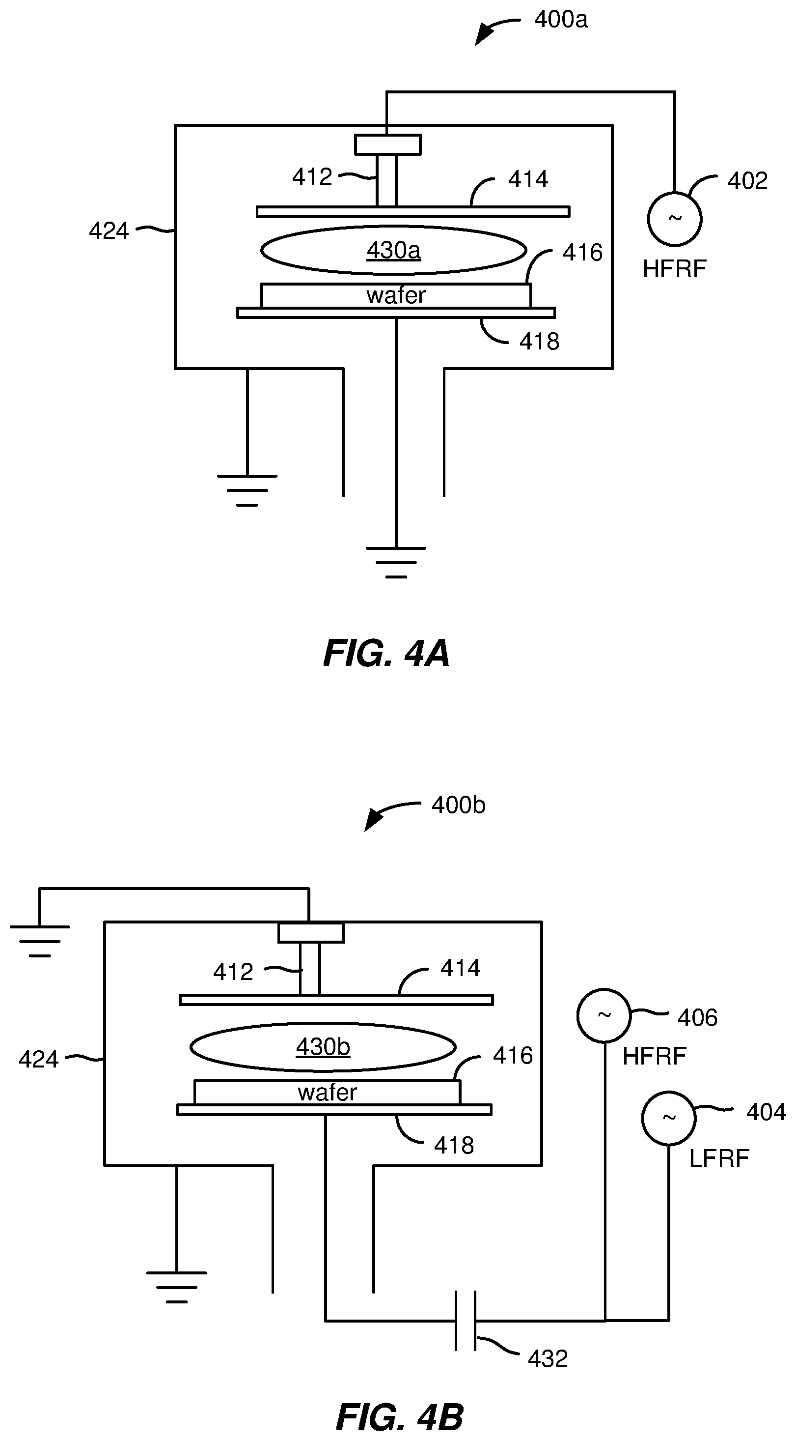
2. The apparatus of claim 1, wherein the process chamber is a capacitively-coupled plasma (CCP) reactor, and wherein the showerhead includes a top electrode and the pedestal includes a bottom electrode.
3. The apparatus of claim 1, further comprising: one or more switches operatively coupled to the one or more RF generators.
4. The apparatus of claim 3, wherein the one or more switches in the deposition mode couple the one or more RF generators to the showerhead.
5. The apparatus of claim 3, wherein the one or more switches in the etch mode couple the one or more RF generators to the pedestal and ground the showerhead.
6. The apparatus of claim 1, wherein the one or more RF generators include an HFRF generator and a LFRF generator.
7. The apparatus of claim 6, wherein the one or more switches include: a first station relay switch configured to electrically connect the LFRF generator and the HFRF generator to the showerhead in the deposition mode; and a second station relay switch configured to electrically connect the LFRF generator and the HFRF generator to the pedestal in the etch mode.
Description
INCORPORATION BY REFERENCE
An Application Data Sheet is filed concurrently with this specification as part of the present application. Each application that the present application claims benefit of or priority to as identified in the concurrently filed Application Data Sheet is incorporated by reference herein in its entirety and for all purposes.
BACKGROUND
The fabrication of integrated circuits includes many diverse processing steps. One of the operations frequently employed is the deposition of a dielectric film into a gap between features patterned over or into semiconductor wafers. One of the goals in depositing such material is to form a void-free, seam-free fill in the gap.
While deposition methods such as high density plasma (HDP), sub-atmospheric chemical vapor deposition (SACVD), and low pressure chemical vapor deposition (LPCVD) have been used for gap fill, these methods do not achieve the desired fill capability and conformality. Flowable chemical vapor deposition and spin-on dielectric (SOD) methods can achieve the desired fill, but tend to deposit highly porous films. Further, these methods are especially complex and costly to integrate, as they require many extra processing steps. Atomic layer deposition (ALD) processes have also been used for gap fill for improved conformality, but these processes suffer from long processing times and low throughput, especially for large gaps. Furthermore, the conformal nature of ALD processes means that the aspect ratios of the gaps increase with successive cycles. Hence, the top of a gap may fill more quickly than the bottom, preventing further diffusion of precursor materials into the gap. Areas can expand such that voids may form in the middle of high aspect ratio gaps.
In some cases, multi-step deposition processes are used, including deposition-etch-deposition processes which require distinct etching operations between subsequent deposition operations. The etching may be done to remedy or prevent void formation in the gap. Specifically, the etch step can be an anisotropic etch that creates a tapered positive slope profile so that gap fill can occur by depositing a subsequent layer on a positive tapered slope rather than a vertical slope. This can minimize the occurrence of void formation in the gap. Voids may lead to high resistance, contamination, loss of filled materials, and otherwise degrade performance of integrated circuits.
SUMMARY
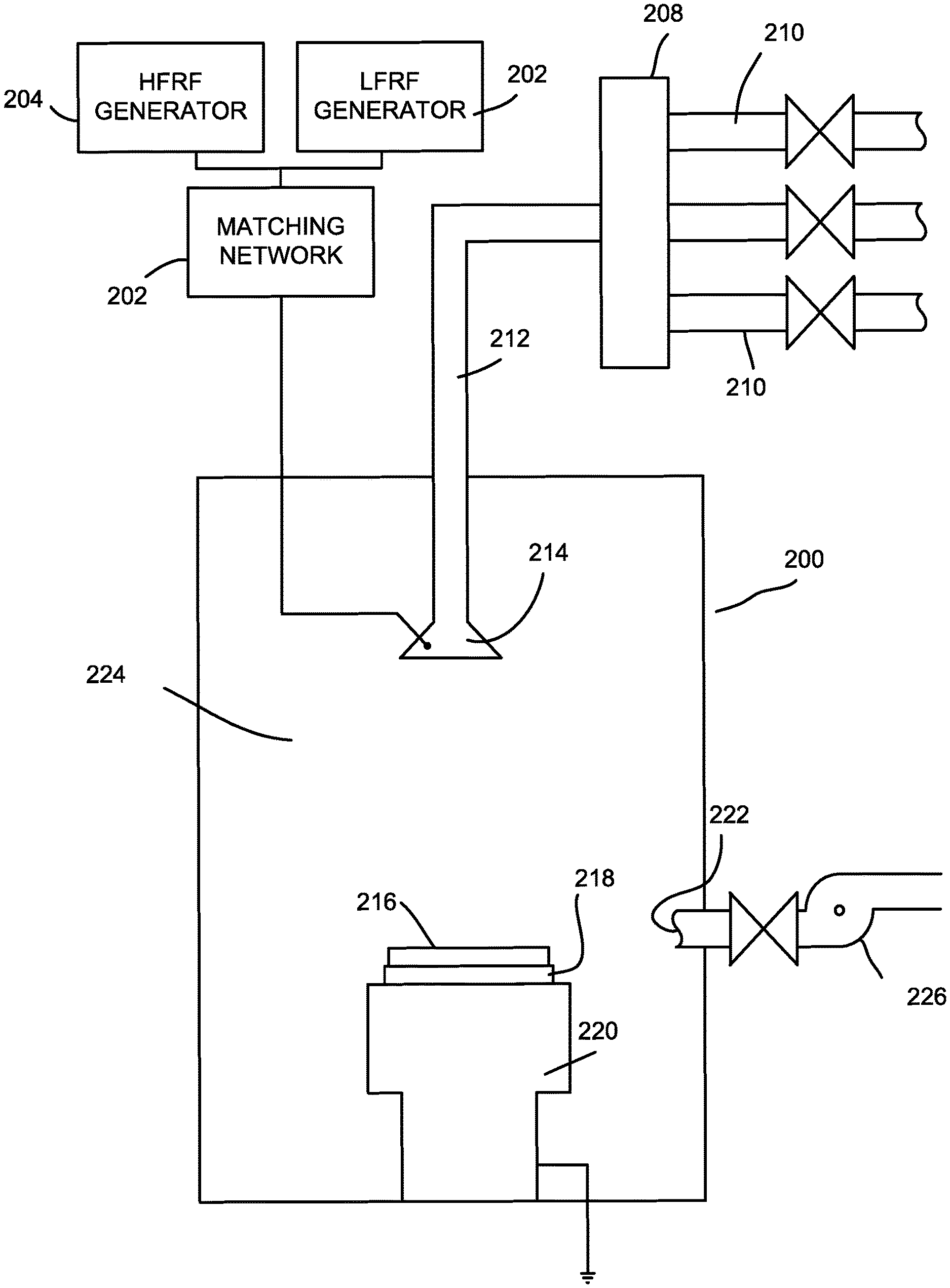
This disclosure pertains to an integrated apparatus for performing deposition and etch processes. The integrated apparatus includes a process chamber, where the process chamber includes a showerhead and a pedestal. The integrated apparatus further includes a low-frequency radio-frequency (LFRF) generator, a high-frequency radio-frequency (HFRF) generator, and one or more switches operatively coupled to one or both of the LFRF generator and the HFRF generator. The one or more switches are configured to switch between (1) a deposition mode for performing a deposition process, where the one or more switches in the deposition mode couple at least the HFRF generator to the showerhead, and (2) an etch mode for performing an etch process, where the one or more switches in the etch mode couple the HFRF generator and the LFRF generator to the pedestal and ground the showerhead
In some implementations, the process chamber is a capacitively-coupled plasma (CCP) reactor, and the showerhead includes a top electrode and the pedestal includes a bottom electrode. In some implementations, the one or more switches in the deposition mode couple the HFRF generator and the LFRF generator to the showerhead and ground the pedestal. In some implementations, the one or more switches include a first station relay switch configured to electrically connect the LFRF generator and the HFRF generator to the showerhead in the deposition mode, and a second station relay switch configured to electrically connect the LFRF generator and the HFRF generator to the pedestal in the etch mode. In some implementations, the first station relay switch is configured to switch to a first position to electrically connect the LFRF generator and the HFRF generator to the showerhead and switch to a second position to ground the showerhead, and the second station relay switch is configured to switch to a first position to electrically connect the LFRF generator and the HFRF generator to the pedestal and switch to a second position to ground the pedestal, where the first position of the first station relay switch is synchronized with the second position of the second station relay switch, and the first position of the second station relay switch is synchronized with the second position of the first station relay switch. In some implementations, the LFRF generator is part of a first integrated circuit board and the HFRF generator is part of a second integrated circuit board. In some implementations, the one or more switches include a switch operatively coupled to the HFRF generator and configured to switch between delivering power from the HFRF generator to the showerhead in the deposition mode and delivering power from the HFRF generator to the pedestal in the etch mode.
This disclosure also pertains to an integrated apparatus for performing deposition and etch processes. The integrated apparatus includes a process chamber, where the process chamber includes a showerhead and a pedestal. The integrated apparatus further includes an integrated circuit board, where the integrated circuit board includes one or more HF/LF RF generators. The integrated apparatus further includes one or more switches operatively coupled to the one or more HF/LF RF generators, the one or more switches configured to switch between (1) a deposition mode for performing a deposition process, wherein the one or more switches in the deposition mode couple at least one of the HF/LF RF generators to the showerhead, and (2) an etch mode for performing an etch process, wherein the one or more switches in the etch mode couple at least one of the HF/LF RF generators to the pedestal.
In some implementations, the process chamber is a CCP reactor, and wherein the showerhead includes a top electrode and the pedestal includes a bottom electrode. In some implementations, the integrated circuit board includes a single HF/LF RF generator. In some implementations, the one or more switches include a first station relay switch configured to electrically connect one of the HF/LF RF generators to the showerhead in the deposition mode, and a second station relay switch configured to electrically connect one of the HF/LF RF generators to the pedestal in the etch mode. In some implementations, the first station relay switch is configured to switch to a first position to electrically connect one of the HF/LF RF generators to the showerhead in the deposition mode and switch to a second position to ground the showerhead, and the second station relay switch is configured to switch to a first position to electrically connect one of the HF/LF RF generators to the pedestal in the etch mode and switch to a second position to ground the pedestal, where the first position of the first station relay switch is synchronized with the second position of the second station relay switch, and the first position of the second station relay switch is synchronized with the second position of the first station relay switch. In some implementations, the one or more switches further include a pedestal grounding relay switch to ground the pedestal in the deposition mode when one of the HF/LF RF generators are operatively coupled to the showerhead, and a showerhead grounding relay switch to ground the showerhead in the etch mode when one of the HF/LF RF generators are operatively coupled to the pedestal.
This disclosure also pertains to a method of filling one or more gaps in a wafer. The method includes providing a wafer on a pedestal in a plasma processing chamber, where the wafer has one or more gaps each having a depth to width aspect ratio of greater than about 5:1, depositing, in the plasma processing chamber, a first dielectric layer in the one or more gaps via ALD, anisotropically etching with slope control, in the plasma processing chamber, the first dielectric layer, and depositing, in the plasma processing chamber, a second dielectric layer in the one or more gaps over the first dielectric layer via ALD.
In some implementations, a wafer temperature is between about 80.degree. C. and about 400.degree. C. while depositing the first dielectric layer, while anisotropically etching with slope control the first dielectric layer, and while depositing the second dielectric layer. In some implementations, a pressure is between about 0.3 and about 1.0 Torr while depositing the first dielectric layer, while anisotropically etching with slope control the first dielectric layer, and while depositing the second dielectric layer. In some implementations, the method further includes switching to apply a low-frequency power and a high-frequency power to the pedestal in the plasma processing chamber and to ground a showerhead in the plasma processing chamber prior to anisotropically etching with slope control the first dielectric layer, and switching to apply the high-frequency power to the showerhead in the plasma processing chamber and to ground the pedestal in the plasma processing chamber prior to depositing the second dielectric layer.
These and other embodiments are described further below with reference to the figures.
BRIEF DESCRIPTION OF THE DRAWINGS
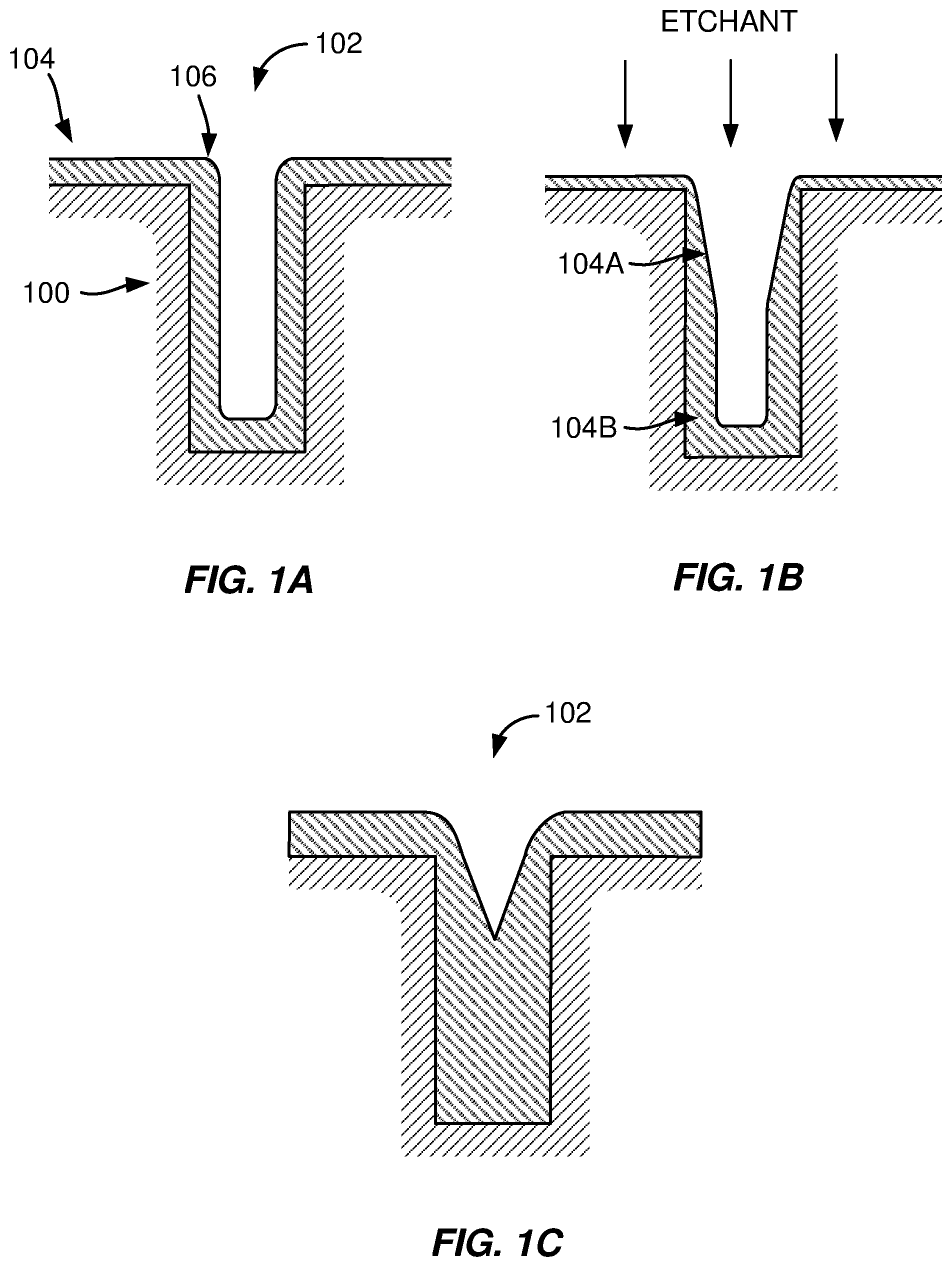
FIGS. 1A-1C depict example cross-sections of a wafer with a gap at various phases of a deposition-etch-deposition gap fill process.
FIG. 2 shows a schematic illustration of an example apparatus for carrying out deposition processes in a conventional deposition-etch-deposition gap fill process.
FIG. 3 shows a schematic illustration of an example multi-station processing tool.
FIG. 4A shows a schematic illustration of an example apparatus including a capacitively-coupled plasma (CCP) reactor for carrying out deposition processes.
FIG. 4B shows a schematic illustration of an example apparatus including a CCP reactor for carrying out etch processes.
FIGS. 5A and 5B each shows a schematic illustration of an example integrated apparatus including a plasma processing chamber configured to switch between a deposition mode and an etch mode according to some implementations.
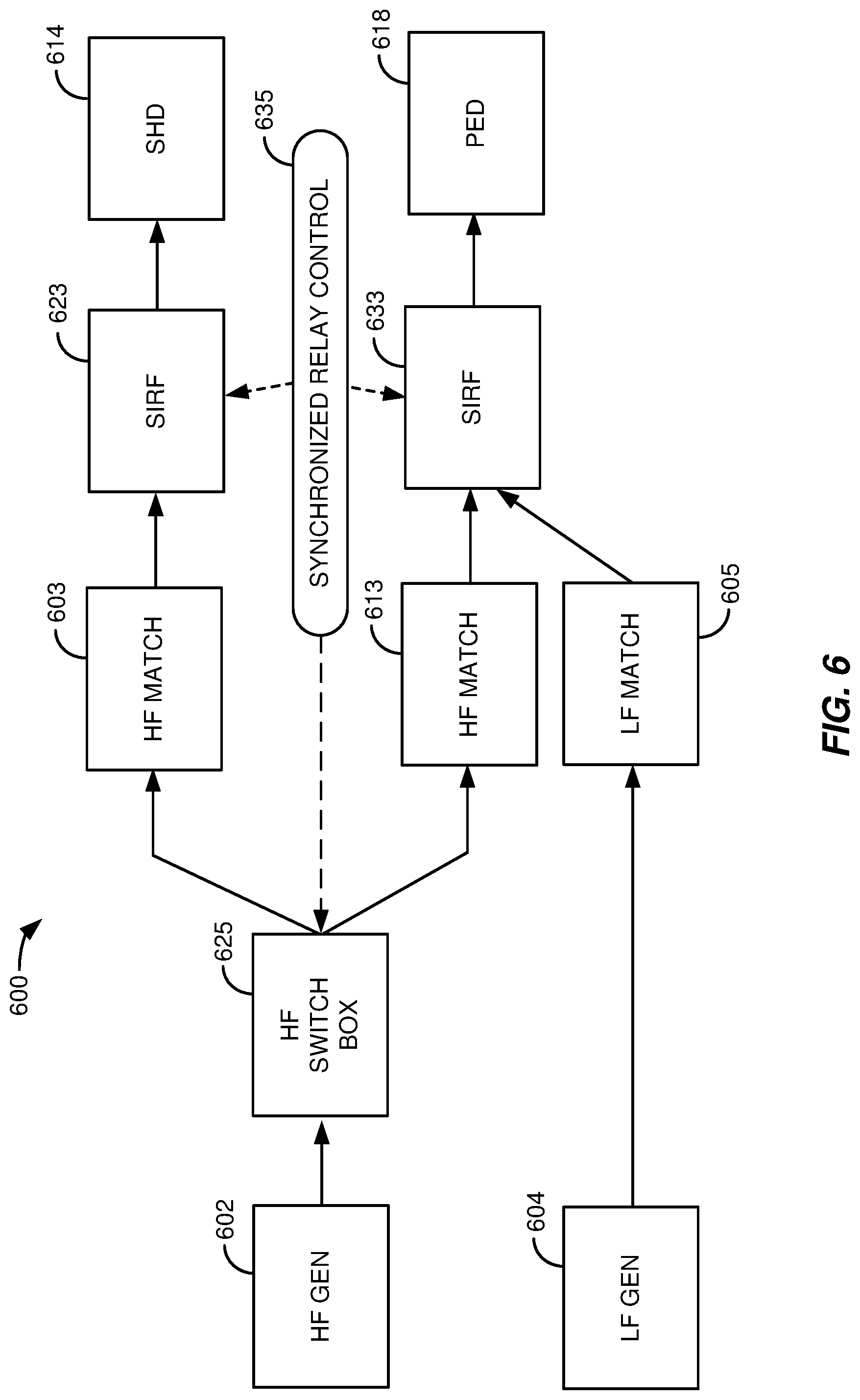
FIG. 6 shows a block diagram of an example scheme for switching between a deposition mode and an etch mode according to some implementations.
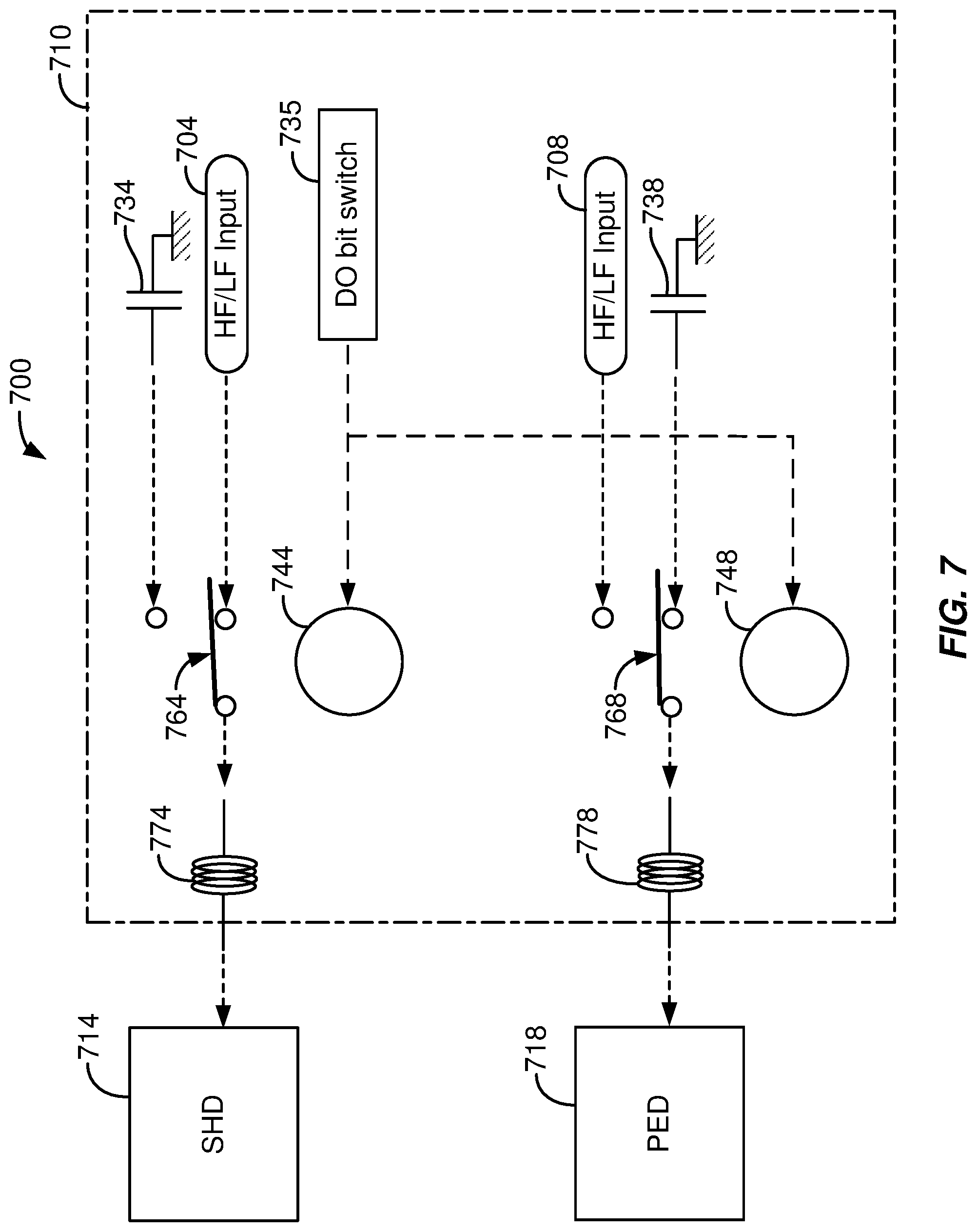
FIG. 7 shows a block diagram of an alternative example scheme for switching between a deposition mode and an etch mode according to some implementations.
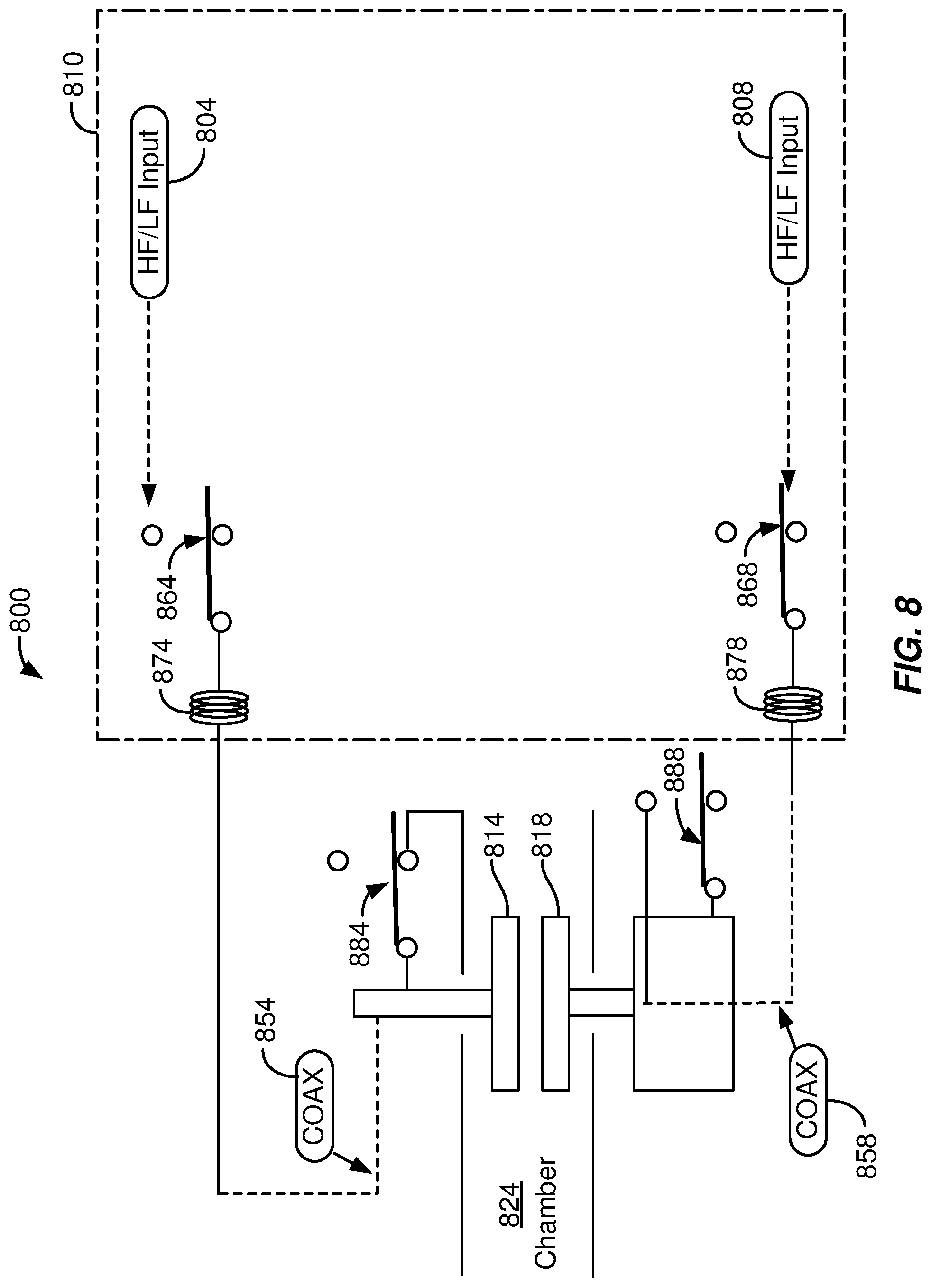
FIG. 8 shows a schematic illustration of an example integrated apparatus including a plasma processing chamber configured to switch between a deposition mode and an etch mode according to some implementations.
FIG. 9A shows a schematic illustration of an example conventional multi-station processing tool for carrying out deposition-etch-deposition gap fill processes.
FIG. 9B shows a schematic illustration of an example multi-station processing tool including a disclosed integrated apparatus for carrying out deposition-etch-deposition gap fill processes.
FIG. 10 shows a flow diagram illustrating an example process flow for performing a deposition-etch-deposition gap fill process on a wafer.
DETAILED DESCRIPTION
Introduction
In the following description, numerous specific details are set forth in order to provide a thorough understanding of the presented concepts. The presented concepts may be practiced without some or all of these specific details. In other instances, well known process operations have not been described in detail so as to not unnecessarily obscure the described concepts. While some concepts will be described in conjunction with the specific embodiments, it will be understood that these embodiments are not intended to be limiting.
In this application, the terms "semiconductor wafer," "wafer," "substrate," "wafer substrate," and "partially fabricated integrated circuit" are used interchangeably. One of ordinary skill in the art would understand that the term "partially fabricated integrated circuit" can refer to a silicon wafer during any of many stages of integrated circuit fabrication thereon. A wafer or substrate used in the semiconductor device industry typically has a diameter of 200 mm, or 300 mm, or 450 mm. The following detailed description assumes the invention is implemented on a wafer. However, the invention is not so limited. The work piece may be of various shapes, sizes, and materials. In addition to semiconductor wafers, other work pieces that may take advantage of this invention include various articles such as printed circuit boards, magnetic recording media, magnetic recording sensors, mirrors, optical elements, micro-mechanical devices and the like.
As circuit densities increase in the semiconductor industry, the width of gaps or trenches in a wafer decrease, thereby increasing their aspect ratios and making it progressively more difficult to fill the gaps or trenches without leaving voids. The formation of voids when the gap is not filled completely can have adverse effects on the operation of a completed device.
Deposition-etch-deposition sequences are employed to remedy or eliminate the presence of voids in gap fill. Common deposition techniques that are used in deposition-etch-deposition sequences are ALD, CVD, plasma-enhanced CVD, and HDP-CVD. A deposition step may be followed by an etch step, such as a sputter etch in HDP applications or reactive ion etch (ME) in ALD applications. The etch step may be an anisotropic etch step that creates a tapered positive slope profile. As a result, more material may be removed near the opening of the gap than from inside the gap.
FIGS. 1A-1C depict example cross-sections of a wafer with a gap at various phases of a deposition-etch-deposition gap fill process. FIG. 1A shows a cross-section of a non-planar wafer 100 including a gap 102. The gap width can vary according to various embodiments, which may range from about 5 .ANG. to about 50 .mu.m. Depth to width aspect ratios can be greater than about 2:1, or greater than about 5:1, or greater than about 10:1, or even greater than about 30:1. The gap 102 can be covered with a thin film 104 using any suitable deposition technique, such as ALD, CVD, plasma-enhanced CVD, and HDP-CVD. In some embodiments, the thin film 104 can be conformal or nearly conformal with the gap 102. As shown in FIG. 1A, the thin film 104 includes a re-entrant portion 106 near the top of the gap 102.
In FIG. 1B, an anisotropic etch is applied to the thin film 104. The re-entrant portion 106 of the thin film 104 can be selectively removed by the anisotropic etch so that an upper region 104a of the thin film 104 is thinner than a lower region 104b. For example, an anisotropic etch may be achieved by imposing mass transfer limitations and/or lifetime limitations on the active etch species. In some implementations, selective etching at the top of the gap 102 may also adjust a sidewall angle of the gap 102, so that the gap 102 is wider at the top than at the bottom. This may further reduce bread loafing effects in subsequent deposition phases.
In FIG. 1C, a subsequent deposition step is applied to fill or nearly fill the gap 102. In some implementations, the gap 102 may be filled after multiple deposition-etch-deposition sequences. The gap 102 may be free of voids. The gap 102 can be filled using any suitable deposition technique, such as ALD, CVD, plasma-enhanced CVD, HDP-CVD, etc.
Common gap fill processes may employ HDP-CVD systems. HDP-CVD systems form a plasma that can be at least approximately two orders of magnitude greater than the density of a standard CCP-CVD systems. HDP-CVD systems are typically inductively-coupled plasma (ICP) systems. An example HDP-CVD system with an ICP reactor to accomplish deposition and etch is the Speed.TM. system available from Lam Research Corporation of Fremont, Calif. Some HDP-CVD techniques promote sputtering by the high density of the plasma, which can occur simultaneous with film deposition. As a result, deposition and etch can be said to occur simultaneously, as the sputtering component of HDP deposition processes slows deposition of certain features, such as corners or raised surfaces, thereby contributing to improved gap fill. However, the sputtering in such HDP-CVD techniques may lead to undesirable redeposition of material on sidewalls of the gap. Some HDP-CVD techniques may employ separate deposition and etch steps. During the etch step, material may be non-conformally removed by an anisotropic sputter etch. Material in the corners may be removed over short distances along the sidewalls of the gap. However, such an anisotropic sputter etch can result in redeposition cusps that can hinder gap filling. Even though HDP-CVD techniques may perform gap fill processes in a single chamber or apparatus, the deposited film from HDP-CVD techniques is not conformal and may actually limit the application of deposition-etch-deposition sequences to be performed in a single chamber or apparatus.
Given the limitations of HDP-CVD techniques in performing gap fill, ALD processes may be used to provide improved conformality. In contrast to CVD processes, ALD processes use surface-mediated deposition reactions to deposit films on a layer-by-layer basis. In some implementations, ALD processes may be performed in a CCP system, such as in a CCP system illustrated in FIG. 2. The CCP system may be capable of supplying high-frequency RF power to generate a plasma. An example of such a CCP system is the Vector.TM. system available from Lam Research Corporation of Fremont, Calif.
FIG. 2 shows a schematic illustration of an example apparatus for carrying out deposition processes in a conventional deposition-etch-deposition gap fill process. As shown in FIG. 2, an apparatus 200 includes a process chamber 224, which encloses other components of the apparatus 200 and serves to contain the plasma. The process chamber 224 includes a showerhead 214 for delivering process gases into the process chamber 224. A high-frequency radio-frequency (HFRF) generator 204 may be connected to an impedance matching network 206, which is connected to the showerhead 214. In some implementations, a low-frequency radio-frequency (LFRF) generator 202 may be connected to the impedance matching network 206 to connect to the showerhead 214. The power and frequency supplied by the impedance matching network 306 is sufficient to generate a plasma from the process gas. In typical processes, a frequency generated by the HFRF generator 204 is between about 2-60 MHz, such as 13.56 MHz or 27 MHz. A frequency generated by the LFRF generator 202 is between about 250-400 kHz, such as 350 kHz or 400 kHz.
The process chamber 224 further includes a wafer support or pedestal 218. The pedestal 218 can support a wafer 216. The pedestal 218 can include a chuck, a fork, and/or lift pins to hold the wafer 216 during and between processing. In some implementations, the chuck may be an electrostatic chuck.
Process gases are introduced via inlet 212. One or more source gas lines 210 can be connected to a manifold 208. The process gases may be premixed or not. Appropriate valving and mass flow control mechanisms are employed to ensure that the correct gases are delivered during deposition, etch, and other plasma treatment operations. Process gases may exit the process chamber 224 via an outlet 222. A vacuum pump 226 can typically draw process gases out and maintain a suitably low pressure within the process chamber 224.
As shown in FIG. 2, the apparatus 200 is a capacitor type system where the showerhead 214 is an electrode working in conjunction a grounded block 220. In other words, the apparatus 200 is a CCP system and may be capable of supplying high-frequency RF power to the top of the process chamber 224, namely the showerhead 214. The bottom of the process chamber 224, namely the pedestal 218 and the block 220, is grounded.
One or more apparatuses for performing deposition-etch-deposition sequences, such as the apparatus 200, may be implemented in a multi-station processing tool. FIG. 3 shows a schematic illustration of an example multi-station processing tool. The multi-station processing tool 300 may include an inbound load lock 302 and an outbound load lock 304, either or both of which may comprise a plasma source. A robot 306, at atmospheric pressure, is configured to move wafers from a cassette loaded through a pod 308 into the inbound load lock 302 via an atmospheric port 310. A wafer is placed by the robot 306 on a pedestal 312 in the inbound load lock 302, the atmospheric port 310 is closed, and the load lock 302 is pumped down. Where the inbound load lock 302 comprises a plasma source, the wafer may be exposed to a plasma treatment in the load lock 312 prior to being introduced to a process chamber 314. Further, the wafer may be heated in the inbound load lock 302 as well, for example, to remove moisture and adsorbed gases. Next a chamber transport port 316 to the process chamber 314 is opened, and another robot (not shown) places the wafer into the reactor on a pedestal of a first station shown in the reactor for processing. While the embodiment depicted in FIG. 3 includes load locks, it will be appreciated that, in some embodiments, direct entry of a wafer into a process station may be provided.
The depicted process chamber 314 includes four process stations, numbered 1 to 4 in the embodiment shown in FIG. 3. Each station can have a heated pedestal (shown at 318 for station 1), and gas line inlets. It will be appreciated that in some embodiments, each process station may have different or multiple purposes. For example, in some embodiments, a process station may be switchable between an ALD and PECVD mode. As discussed later according to the present disclosure, in some embodiments, a process station may include a CCP reactor that is switchable between a deposition mode and an etch mode. While the depicted process chamber 314 comprises four stations, it will be understood that a process chamber 314 according to the present disclosure may have any suitable number of stations. For example, in some embodiments, a process chamber 314 may have five or more stations, while in other embodiments a process chamber 314 may have three or fewer stations.
FIG. 3 also depicts a wafer handling system 390 for transferring wafers within the process chamber 314. In some embodiments, wafer handling system 390 may transfer wafers between various process stations and/or between a process station and a load lock. It will be appreciated that any suitable wafer handling systems may be employed. Non-limiting examples include wafer carousels and wafer handling robots. FIG. 3 also depicts a system controller 350 employed to control process conditions and hardware states of the multi-station processing tool 300. System controller 350 may include one or more memory devices 356, one or more mass storage devices 354, and one or more processors 352. Processor 352 may include a CPU or computer, analog and/or digital input/output connections, stepper motor controller boards, etc.
In some embodiments, system controller 350 controls all of the activities of the multi-station process tool 300. System controller 350 executes system control software 358 stored in mass storage device 354, loaded into memory device 356, and executed on processor 352. System control software 358 may include instructions for controlling the timing, mixture of gases, chamber and/or station pressure, chamber and/or station temperature, purge conditions and timing, wafer temperature, RF power levels, RF frequencies, wafer and/or pedestal position, deposition and etch mode switching, and other parameters of a particular process performed by multi-station process tool 300. System control software 358 may be configured in any suitable way. For example, various process tool component subroutines or control objects may be written to control operation of the process tool components necessary to carry out various process tool processes in accordance with the disclosed methods. System control software 358 may be coded in any suitable computer readable programming language.
In some embodiments, system control software 358 may include input/output control (IOC) sequencing instructions for controlling the various parameters. For example, each phase of an ALD process may include one or more instructions for execution by system controller 350. In addition, switching from a deposition mode to an etch mode may include one or more instructions for execution by the system controller 350. The instructions for setting process conditions for an ALD process may be included in a corresponding ALD recipe phase, and the instructions for setting process conditions for an anisotropic etch process may be included in a corresponding etch recipe phase. In some implementations, the ALD and etch recipe phases may be sequentially arranged.
Other computer software and/or programs stored on mass storage device 354 and/or memory device 356 associated with system controller 350 may be employed in some embodiments. Examples of programs or sections of programs for this purpose include a wafer positioning program, a process gas control program, a pressure control program, a heater control program, and a plasma control program.
A wafer positioning program may include program code for process tool components that are used to load the wafer onto pedestal 318 and to control the spacing between the wafer and other parts of process tool 300.
A process gas control program may include code for controlling gas composition and flow rates and optionally for flowing gas into one or more process stations prior to deposition in order to stabilize the pressure in the process station. A pressure control program may include code for controlling the pressure in the process station by regulating, for example, a throttle valve in the exhaust system of the process station, a gas flow into the process station, etc.
A heater control program may include code for controlling the current to a heating unit that is used to heat the wafer. Alternatively, the heater control program may control delivery of a heat transfer gas (such as helium) to the wafer.
A plasma control program may include code for setting RF power levels applied to the process electrodes in one or more process stations.
In some embodiments, there may be a user interface associated with system controller 350. The user interface may include a display screen, graphical software displays of the apparatus and/or process conditions, and user input devices such as pointing devices, keyboards, touch screens, microphones, etc.
In some embodiments, parameters adjusted by system controller 350 may relate to process conditions. Non-limiting examples include process gas composition and flow rates, deposition and etch mode, wafer temperature, pressure, plasma conditions (such as RF power levels), etc. These parameters may be provided to the user in the form of a recipe, which may be entered utilizing the user interface.
Signals for monitoring the process may be provided by analog and/or digital input connections of system controller 350 from various process tool sensors. The signals for controlling the process may be output on the analog and digital output connections of the multi-station process tool 300. Non-limiting examples of process tool sensors that may be monitored include mass flow controllers, pressure sensors (such as manometers), thermocouples, etc. Appropriately programmed feedback and control algorithms may be used with data from these sensors to maintain process conditions.
System controller 350 may provide program instructions for implementing the disclosed processes, including the deposition-etch-deposition gap fill processes. The program instructions may control a variety of process parameters, such as DC power level, RF power level, RF bias power level, pressure, wafer temperature, etc. The instructions may control the parameters to operate deposition-etch-deposition sequences according to various embodiments described herein.
Deposition and Etch Modes
Typically, deposition in a CCP reactor may occur in certain hardware configurations, and etch in a CCP reactor may occur in different hardware configurations. Specifically, ALD in a CCP reactor may be optimized according to certain RF hardware configurations, and etch in a CCP reactor may be optimized according to different RF hardware configurations. FIGS. 4A and 4B show different RF hardware configurations for performing deposition and etch in a CCP reactor. In FIG. 4A, the wafer is supported on a grounded electrode for deposition and the top electrode is powered. In FIG. 4B, the wafer is supported on a powered electrode for etch and the top electrode is grounded.
FIG. 4A shows a schematic illustration of an example apparatus including a CCP reactor for carrying out deposition processes. An apparatus 400a includes a CCP reactor 424 capable of performing PECVD or ALD. The CCP reactor 424 includes a showerhead 414 that serves as a top electrode and a pedestal 418 that serves as a bottom electrode. The pedestal 418 is below and opposite the showerhead 414 and may support a wafer 416 to be processed. In some implementations, the wafer 416 may have one or more features so that the wafer 416 is not planar. For example, the wafer 416 may have one or more gaps or a plurality of gaps. In some embodiments, the pedestal 418 may be raised or lowered. Process gases are introduced to the showerhead 414 via gas inlet 412, and the showerhead 414 distributes the process gases into the CCP reactor 424 and towards the wafer 416. An RF power supply 402 may be electrically connected to the showerhead 414 for generating a plasma 430a in a volume between the showerhead 414 and the wafer 416. The plasma 430a in the hardware configuration of FIG. 4A can be optimized for deposition. In some embodiments, the plasma energy can be controlled by controlling one or more of chamber pressure, gas concentration, gas mixture, RF source power, RF source frequency, duty cycle, pulse frequency, etc.
FIG. 4A illustrates an example RF hardware configuration for deposition, where the RF power supply 402 can be an HFRF generator electrically connected to the showerhead 414 and where the pedestal 418 is grounded. The RF hardware configuration of FIG. 4A is generally not capable of providing sufficient etch rates because an insufficient voltage drop across the wafer 416 would be produced. However, the RF hardware configuration of FIG. 4A is capable of fast frequency tuning, which can be important in ALD applications.
Fast frequency tuning is what allows for impedance matching to occur quickly in the RF hardware configuration of FIG. 4A. Impedance matching is the practice of designing the input impedance of an electrical load or the output impedance of its corresponding signal source in order to maximize the power transfer and minimize reflection from the load. In a plasma processing context, impedance matching is used to minimize the reflected power back from a plasma discharge into the transmission line (e.g., RF cables), and maximize the power transferred from an RF power supply 402 into the plasma discharge. In addition, if the RF power supply 402 is not matched, there is reflected power that builds standing waves on a transmission line between the source (RF power supply 402) and the load (plasma 430a), which can lead to further power waste and cause frequency-dependent loss. In some implementations, an impedance matching network (not shown) can be coupled to the RF power supply 402. The impedance matching network can transform the load impedance presented from the plasma 430a to match the source impedance of the RF power supply 402. Typically, the impedance matching network can be equipped with one or more capacitors or inductors to tune the impedance of the RF power supply 402 to match the plasma impedance. However, tuning the impedance using capacitors or inductors can be a long process, which can be undesirable in applications that require short plasma on-times. For example, to operate in an ALD window, processes can take on the order of 0.5 seconds or less. So rather than matching impedance using capacitors or inductors, impedance matching can occur by simply switching the frequency of the RF power supply 402. To illustrate, if the impedance of the RF power supply 402 needs to match the plasma impedance at 50 ohms, then the RF power supply 402 can quickly switch from operating at 13.56 MHz to 13.8 MHz. This kind of fast frequency tuning may not be possible in other RF hardware configurations, such as what is illustrated in FIG. 4B.
FIG. 4B shows a schematic illustration of an example apparatus including a CCP reactor for carrying out etch processes. The apparatus 400b includes a CCP reactor 424 capable of performing plasma etching. Like the apparatus 400a in FIG. 4A, the apparatus 400b in FIG. 4B includes a showerhead 414, a pedestal 418, a wafer 416, and a gas inlet 412. An RF power supply 404, 406 may be electrically connected to the pedestal 418 for applying a voltage drop across the wafer 416. The RF power supply 404, 406 may include both an LFRF generator 404 and an HFRF generator 406. A plasma 430b may be generated in a volume between the showerhead 414 and the wafer 416. The plasma 430b in the hardware configuration of FIG. 4B may be optimized for etching.
FIG. 4B illustrates an example RF hardware configuration for etching, where the LFRF generator 404 and the HFRF generator 406 can be electrically connected to the pedestal 418 and where the showerhead 414 is grounded. In some implementations, the LFRF generator 404 can provide a low-frequency RF signal between about 2 Hz and about 1000 kHz, such as 400 kHz. In some implementations, the HFRF generator 406 can provide a high-frequency RF signal between about 1 MHz and about 100 MHz, such as 13.56 MHz. A blocking capacitor 432 can be positioned between the pedestal 418 and both the LFRF generator 404 and the HFRF generator 406. With both high-frequency and low-frequency signals being mixed, the blocking capacitor 432 can serve as a filter leading to the pedestal 418. The RF configuration of FIG. 4B is not capable of fast frequency tuning. This is due in part to the number of components in the RF path that would prevent the fast response necessary for frequency tuning. Accordingly, ALD processes would generally not be able to operate in such conditions where the pedestal 418 is biased in FIG. 4B. However, unlike the RF configuration of FIG. 4A, the RF configuration of FIG. 4B is able to provide a high voltage drop across the wafer 416.
Deposition-Etch-Deposition Integrated Apparatus
Rather than performing deposition and etch in an RF hardware configuration that is optimal for one process but not the other, and rather than constantly transferring a wafer from one apparatus to another for implementing deposition-etch-deposition sequences, the present disclosure provides for an integrated apparatus that is optimal for both deposition and etch, and that integrates deposition-etch-deposition sequences in a single apparatus. An integrated apparatus can provide an RF hardware configuration that is optimal for both deposition and etch modes using a combination of different hardware components, such as relay switches, DO bit switches, integrated circuit boards (e.g., splitter boards), RF generators, coaxial cables, switchboxes, RF filters, match units, etc.
FIG. 5A shows a schematic illustration of an example integrated apparatus including a plasma processing chamber configured to switch between a deposition mode and an etch mode according to some implementations. The integrated apparatus 500 includes a plasma processing chamber 524, where the plasma processing chamber 524 includes a showerhead 514 for delivering process gases and a pedestal 518 for supporting a wafer. The plasma processing chamber 524 can be a CCP reactor, where the showerhead 514 includes a top electrode and the pedestal 518 includes a bottom electrode. The integrated apparatus 500 can include multiple power sources for supplying RF power to the showerhead 514 and the pedestal 518. In some implementations, the integrated apparatus 500 can include an LFRF generator 504 and an HFRF generator 502. The LFRF generator 504 and the HFRF generator 502 may be operatively coupled to the showerhead 514 or the pedestal 518 via one or more switches 564, 568. As used herein, components that are "operatively coupled" with one another refer to components that are in electrical connection or otherwise coupled with one another depending on the operations of a controlling device (e.g., switch, system controller, etc.). The integrated apparatus 500 can include one or more switches 564, 568 operatively coupled to one or both of the LFRF generator 504 and the HFRF generator 502. The switches 564, 568 may be configured to switch between (1) a deposition mode for performing a deposition process, where the switches 564, 568 couple at least the HFRF generator 502 to the showerhead 514, and (2) an etch mode for performing an etch process, where the switches 564, 568 couple at least the LFRF generator 504 and the HFRF generator 502 to the pedestal 518 and grounds the showerhead 514. When the HFRF generator 502 is coupled to the showerhead 514 in the deposition mode, the HFRF generator 502 can deliver RF power to the showerhead 514. When the HFRF generator 502 and the LFRF generator 504 are coupled to the pedestal 518 in the etch mode, the HFRF generator 502 and the LFRF generator 504 can deliver RF power to the pedestal 518.
In FIG. 5A, the switches 564, 568 can be replaced by filters 534, 536 as shown in FIG. 5B, where the filters 534 536 can switch between (1) a deposition mode for performing a deposition process, where the filters 534 536 couple selectively pass high-frequency signals to the showerhead 514, and (2) an etch mode for performing an etch process, where the filters 534 536 selectively pass one or both high-frequency and low-frequency signals to the pedestal 518.
As shown in FIG. 5A, the one or more switches 564, 568 include a first station relay switch 564 configured to couple the LFRF generator 504 and the HFRF generator 502 to the showerhead 514 in the deposition mode. In a first position, the first station relay switch 564 electrically connects the LFRF generator 504 and the HFRF generator 502 to the showerhead 514. That way, the showerhead 514 is powered in the deposition mode. In a second position, the first station relay switch 564 is electrically grounded, so that the showerhead 514 is electrically grounded. As shown in FIG. 5A, the one or more switches 564, 568 include a second station relay switch 568 configured to couple the HFRF generator 502 and the LFRF generator 504 to the pedestal 518 in the etch mode. In a first position, the second station relay switch 568 electrically connects the HFRF generator 502 and the LFRF generator 504 to the pedestal 518. That way, the pedestal 518 is biased in the etch mode. In a second position, the second station relay switch 568 is electrically grounded, so that the pedestal 518 is electrically grounded.
In some implementations as shown in FIGS. 5A and 5B, the integrated apparatus 500 can include a low-frequency match unit 505 (or low-frequency impedance matching network 505) coupled to the LFRF generator 504. In some embodiments, the integrated apparatus 500 can include a high-frequency match unit 503 (or high-frequency impedance matching network 503) coupled to the HFRF generator 502. In some implementations, the integrated apparatus 500 can further include one or more filters to selectively pass high or low frequency signals. The integrated apparatus 500 can include a low-pass filter 554 coupled to the low-frequency match unit 505, and a high-pass filter 552 coupled to the high-frequency match unit 503. In some embodiments, each of the low-pass filter 554 and the high-pass filter 552 includes one or more capacitors and inductors. The low-pass filter 554 can prevent high-frequency signals from getting back to the LFRF generator 504, and the high-pass filter 552 can prevent low-frequency signals from getting back to the HFRF generator 502. In some implementations, each of the low-pass filter 554 and the high-pass filter 552 can serve as RF filters for multiple plasma processing chambers, and not just the plasma processing chamber 524. In some implementations, a blocking filter 532 can be inserted between the LFRF generator 504 and both the pedestal 518 and the showerhead 514 to selectively block high-frequency signals or low-frequency signals. The blocking filter 532 can function similarly to the blocking capacitor 432 in the RF hardware configuration of FIG. 4B.
In FIG. 5A, the integrated apparatus 500 is selectively switchable between a deposition mode and an etch mode. In the deposition mode according to certain embodiments, the first station relay switch 564 is switched to the first position so that the LFRF generator 504 and the HFRF generator 502 is electrically connected to the showerhead 514, and the second station relay switch 568 is simultaneously switched to the second position so that the pedestal 518 is grounded. Such a configuration may be utilized for ALD. In the deposition mode according to alternative implementations, the first station relay switch 564 is switched to the first position so that the LFRF generator 504 and the HFRF generator 502 are electrically connected to the showerhead 514, and the second station relay switch 568 is simultaneously switched to the first position so that the LFRF generator 504 and the HFRF generator 502 is electrically connected to the pedestal 518. In some implementations, the blocking filter 532 can prevent low-frequency signals from reaching the showerhead 514. In the etch mode according to certain implementations, the second station relay switch 568 is switched to the first position so that the LFRF generator 504 and the HFRF generator 502 are electrically connected to the pedestal 518, and the first station relay switch 564 is simultaneously switched to the second position so that the showerhead 514 is grounded. In some implementations, the blocking filter 532 can prevent low-frequency or high-frequency signals from reaching the pedestal 518. In some implementations, both low-frequency and high-frequency signals can be used to bias the pedestal 518 in the etch mode.
The RF hardware configuration of FIG. 5A may optimize deposition and etch modes using switches 564, 568 so that deposition-etch-deposition sequences can be performed in a single integrated apparatus 500. Additionally, the RF hardware configuration of FIGS. 5A and 5B may utilize multiple integrated circuit boards (e.g., splitter boards) to accommodate both the HFRF generator 502 and the LFRF generator 504. The splitter board allows signal to be distributed not only to one plasma processing chamber, such as the plasma processing chamber 524, but to multiple plasma processing chambers. Each splitter board can include multiple stations with multiple channels. One splitter board can include the LFRF generator 504, the low-frequency match unit 505, and the low-pass filter 554, and another splitter board can include the HFRF generator 502, the high-frequency match unit 503, and the high-pass filter 552. In some implementations, the switches 564, 568 may be relay switches capable of at least 4 million, at least 20 million, or at least 25 million cycles.
FIG. 6 shows a block diagram of an example scheme for switching between a deposition mode and an etch mode according to some implementations. Like the RF hardware configuration shown in FIGS. 5A and 5B, an integrated apparatus 600 can include a showerhead 614, a pedestal 618, an HFRF generator 602, an LFRF generator 604, and multiple integrated circuit boards 623, 633 (e.g., splitter boards). The HFRF generator 602 and the LFRF generator 604 may be operatively coupled to the showerhead 614 and the pedestal 618. The integrated apparatus 600 includes a switch 625 operatively coupled to the HFRF generator 602. The switch 625 may be configured to switch between (1) a deposition mode for performing deposition processes, where the switch 625 couples the HFRF generator 602 to the showerhead 614, and (2) an etch mode for performing an etch process, where the switch 625 couples at least the LFRF generator 604 and the HFRF generator 602 to the pedestal 618 and grounds the showerhead 614.
In FIG. 6, the integrated apparatus 600 can include a first integrated circuit board 623 and a first high-frequency match unit 603 associated with the deposition mode. In the deposition mode, the HFRF generator 602 is electrically connected to the showerhead 614 via the switch 625, so that the HFRF generator 602, the first high-frequency match unit 603, and the first integrated circuit board 623 are in electrical connection with the showerhead 614. The HFRF generator 602 and the first high-frequency match unit 603 can deliver power to the showerhead 614 in the deposition mode. In some implementations, the pedestal 618 is grounded in the deposition mode.
In FIG. 6, the integrated apparatus 600 can include a second integrated circuit board 633 and a low-frequency match unit 605 as well as a second high-frequency match unit 613 associated with the etch mode. In the etch mode, the LFRF generator 604 is electrically connected to the pedestal 618, and the HFRF generator 602 is electrically connected to the pedestal 618 via the switch 625. That way, the HFRF generator 602, the second high-frequency match unit 613, the LFRF generator 604, the low-frequency match unit 605, and the second integrated circuit board 633 are in electrical connection with the pedestal 618. The HFRF generator 602 and the second high-frequency match unit 613 as well as the LFRF generator 604 and the low-frequency match unit 605 deliver power to the pedestal 618 in the etch mode. In some implementations, the showerhead 614 is grounded in the etch mode.
In some implementations, the switch 625 is an HFRF switchbox configured to switch between delivering power from the HFRF generator 602 to the showerhead 614 in the deposition mode, and delivering power from the HFRF generator 602 to the pedestal 618 in the etch mode. In the deposition mode, only the HFRF generator 602 is coupled to the showerhead 614 through the first integrated circuit board 623. In the etch mode, both the HFRF generator 602 and the LFRF generator 604 are coupled to the pedestal 618 through the second integrated circuit board 633. In some implementations, the first integrated circuit board 623 and the second integrated circuit board 633 are communicatively coupled via a synchronized relay control 635, and the synchronized relay control 635 is communicatively coupled to the switch 625. The synchronized rely control 635 is configured to synchronize switching between the deposition and etch modes. For example, if the first integrated circuit board 623 is delivering power to the showerhead 614 from the HFRF generator 602 in the deposition mode, then the synchronized relay control 635 can simultaneously communicate to the second integrated circuit board 633 to not deliver power to the pedestal 618. Or, if the second integrated circuit board 633 is delivering power to the pedestal 618 from the HFRF generator 602 and the LFRF generator 604 in the etch mode, then the synchronized relay control 635 can simultaneously communicate to the first integrated circuit board 623 to not deliver power to the showerhead 614.
Whereas the RF hardware configurations in FIGS. 5 and 6 utilize an HFRF generator, an LFRF generator, and separate integrated circuit boards for powering a showerhead and/or pedestal, some RF hardware configurations may mix together the HFRF generator and the LFRF generator as a single power supply source and utilize a single integrated circuit board for powering a showerhead and/or pedestal. In some implementations, the HFRF generator and the LFRF generator may be part of a single integrated circuit board. The single integrated circuit board can deliver high-frequency and/or low frequency signals to a showerhead in one mode, and deliver high-frequency and/or low frequency signals to a pedestal in another mode. The single integrated circuit board can include multiple stations with multiple channels.
FIG. 7 shows a block diagram of an alternative example scheme for switching between a deposition mode and an etch mode according to some implementations. An integrated apparatus 700 can include an integrated circuit board 710, a showerhead 714, and a pedestal 718. The showerhead 714 and the pedestal 718 may be part of a plasma processing chamber (not shown) for performing deposition-etch-deposition sequences on a wafer. The plasma processing chamber can be a CCP reactor, where the showerhead 714 includes a top electrode and the pedestal 718 includes a bottom electrode. The integrated circuit board 710 can include one or more HF/LF RF generators 704, 708 and one or more switches 764, 768, where the one or more switches 764, 768 are configured to switch between (1) a deposition mode for performing a deposition process, where the one or more switches 764, 768 in the deposition mode couples the HF/LF generator 704 to the showerhead 714, and (2) an etch mode for performing an etch process, where the one or more switches 764, 768 in the etch mode couples the HF/LF generator 708 to the pedestal 718. In some implementations, the HF/LF RF generator(s) 704, 708 shown in FIG. 7 can be a single HF/LF RF generator. A single HF/LF RF generator can be capable of delivering both high-frequency and low-frequency signals. The same HF/LF RF generator can be used to power the showerhead 714 or the pedestal 718.
In some embodiments, the integrated circuit board 710 can be outfitted with multiple channels to power up multiple stations. At one of the stations can be a first station relay switch 764, and at one of the other stations can be a second station relay switch 768. The first station relay switch 764 is configured to couple a first HF/LF RF generator 704 to the showerhead 714 in the deposition mode. When the first station relay switch 764 is in a first position, the integrated apparatus 700 is in the deposition mode and the first HF/LF RF generator 704 is electrically connected to the showerhead 714 to power the showerhead 714. The signal from the HF/LF RF generator 704 passes through a first inductor 774 to the showerhead 714. When the first station relay switch 764 is in a second position, the showerhead 714 is grounded. In some implementations, a first capacitor 734 is provided when the showerhead 714 is grounded to compensate for the inductance in the return path. The second station relay switch 768 is configured to couple a second HF/LF RF generator 708 to the pedestal 718 in the etch mode. When the second station relay switch 768 is in a first position, the integrated apparatus 700 is in the etch mode and the second HF/LF RF generator 708 is electrically connected to the pedestal 718 to bias the pedestal 718. The signal from the second station relay switch 768 passes through a second inductor 778 to the pedestal 718. When the second station relay switch 768 is in a second position, the pedestal 718 is grounded. In some implementations, a second capacitor 738 is provided when the pedestal 718 is grounded to compensate for the inductance in the return path.
In some embodiments as shown in FIG. 7, the integrated circuit board 710 includes a switch 735, such as a digital output (DO) bit switch, configured to synchronize switching between modes. The switch 735 can be coupled to a first relay 744 and a second relay 748. In some implementations, each of the first relay 744 and the second relay 748 can be a high voltage vacuum relay. When the switch 735 is in a deposition mode, the first relay 744 can be in an open position and the second relay 748 can be in a closed position. When the switch is in an etch mode, the first relay 744 can be in a closed position and the second relay 748 can be in an open position. When the first relay 744 is opened and the second relay 748 is closed, the first station relay switch 764 is in the first position and the second station relay switch 768 is in the second position so that the showerhead 714 is powered and the pedestal 718 is grounded. When the first relay 744 is closed and the second relay 748 is opened, the first station relay switch 764 is in the second position and the second station relay switch 768 is in the first position so that the pedestal 718 is powered and the showerhead 714 is grounded. Such an arrangement in FIG. 7 allows for the HF/LF RF generator(s) 704, 708 to power the showerhead 714 and ground the pedestal 718 in the deposition mode, or for the HF/LF RF generator(s) 704, 708 to power the pedestal 718 and ground the showerhead 714 in the etch mode.
The showerhead 714 in FIG. 7 may be grounded through a coaxial cable (not shown) positioned between the showerhead 714 and the first inductor 774. The pedestal 718 in FIG. 7 may also be grounded through a coaxial cable positioned between the pedestal 718 and the second inductor 778. However, grounding through an inductor and a coaxial cable creates a longer return path to electrical ground. This can cause more voltage to build up on either the showerhead 714 or the pedestal 718, which can effectively reduce the voltage between electrodes. This can cause the etch mode, for example, to be less effective if the pedestal 718 is biased yet the voltage between the electrodes change.
Rather than grounding through an inductor and a coaxial cable, some RF hardware configurations may ground the showerhead and the pedestal local to the plasma processing chamber. FIG. 8 shows a schematic illustration of an example integrated apparatus including a plasma processing chamber configured to switch between a deposition mode and an etch mode according to some implementations. An integrated apparatus 800 includes an integrated circuit board 810 and a plasma processing chamber 824, where the plasma processing chamber 824 includes a showerhead 814 and a pedestal 818. The plasma processing chamber 824 may be a CCP reactor, where the showerhead 814 includes a top electrode and the pedestal 818 includes a bottom electrode. The CCP reactor may be configured to perform deposition-etch-deposition sequences on a wafer. The integrated circuit board 810 can include one or more HF/LF RF generators 804, 808 and one or more switches 864, 868. The integrated apparatus 800 can further include additional switches 884, 888. The switches 864, 868, 884, 888 are configured to switch between (1) a deposition mode for performing a deposition process, where the switches 864, 868, 884, 888 in the deposition mode couple the HF/LF RF generator 804 to the showerhead 814 and ground the pedestal 818, and (2) an etch mode for performing an etch process, where the switches 864, 868, 884, 888 in the etch mode couple the HF/LF RF generator 808 to the pedestal 818 and ground the showerhead 814. In some implementations, the HF/LF RF generator(s) 804, 808 shown in FIG. 8 can be a single HF/LF RF generator. A single HF/LF RF generator can be capable of delivering both high-frequency and low-frequency signals. The same HF/LF RF generator can be used to power the showerhead 814 or the pedestal 818.
In some implementations, the integrated circuit board 810 can be outfitted with multiple channels to power up multiple stations. At one of the stations can be a first station relay switch 864, and at one of the other stations can be a second station relay switch 868. The first station relay switch 864 is configured to couple a first HF/LF RF generator 804 to the showerhead 814 in the deposition mode. When the first station relay switch 864 is in a first position, the integrated apparatus 800 is in the deposition mode and the first HF/LF RF generator 804 is electrically connected to the showerhead 814 to power the showerhead 814. The signal from the HF/LF RF generator 804 passes through a first inductor 874 to the showerhead 814. When the first station relay switch 864 is in a second position, the showerhead 814 is grounded. However, rather than grounding through the first inductor 874 and a first coaxial cable 854, the showerhead 814 is grounded locally to the plasma processing chamber 824. A showerhead grounding relay switch 884 is provided local to the showerhead 814 and is coupled to a first station associated with the first station relay switch 864. This reduces the inductance in the return path and can eliminate the need for compensation capacitors. The second station relay switch 868 is configured to couple a second HF/LF RF generator 808 to the pedestal 818 in the etch mode. When the second station relay switch 868 is in a first position, the integrated apparatus 800 is in the etch mode and the second HF/LF RF generator 808 is electrically connected to the pedestal 818 to bias the pedestal 818. The signal from the second station relay switch 868 passes through a second inductor 878 to the pedestal 818. When the second station relay switch 868 is in a second position, the pedestal 818 is grounded. However, rather than grounding through the second inductor 878 and a second coaxial cable 858, the pedestal 818 is grounded locally to the plasma processing chamber 824. A pedestal grounding relay switch 888 is provided local to the pedestal 818 and is coupled to a second station associated with the second station relay switch 868. This reduces the inductance in the return path and can eliminate the need for compensation capacitors. In some implementations, locally grounding the electrodes can improve the etch process in the etch mode. However, each station in FIG. 8 is outfitted with two relay switches instead of one, such as having relay switches 864, 884 at a first station and relay switches 868, 888 at a second station.
The integrated circuit board 810 (e.g., splitter board) can include multiple stations, where each station is capable of switching the power on/off. The integrated circuit board 810 can include a DO bit switch (not shown) at one of the stations, where the DO bit switch is configured to synchronize switching between modes. Thus, all four relay switches 864, 868, 884, 888 can be synchronized. For example, if the DO bit switch is provided at a first station associated with the first station relay switch 864, and if the first station relay switch 864 is switched to the first position (e.g., turned on), then the showerhead 814 is powered and the pedestal 818 is grounded. Specifically, the second station relay switch 868 is switched to the second position (e.g., turned off), and the pedestal grounding relay switch 888 locally grounds the pedestal 818. If the first station relay switch 864 is switched to the second position (e.g., turned off), then the pedestal 818 is powered and the showerhead 814 is grounded. Specifically, the second station relay switch 868 is switched to the first position (e.g., turned on), and the showerhead grounding relay switch 884 locally grounds the showerhead 814. Such an arrangement in FIG. 8 allows for the HF/LF RF generator(s) 804, 808 to power the showerhead 814 and ground the pedestal 818 in the deposition mode, or for the HF/LF RF generator(s) 804, 808 to power the pedestal 818 and ground the showerhead 814 in the etch mode.
The aforementioned RF hardware configurations in integrated apparatuses described in FIGS. 5-8 can provide a simpler and more flexible tool solution for performing deposition-etch-deposition sequences than conventional tools. FIG. 9A shows a schematic illustration of an example conventional multi-station processing tool for carrying out deposition-etch-deposition gap fill processes. A multi-station processing tool 900a includes a robot 906 configured to move wafers from a cassette loaded through a pod 908 into a load lock and ultimately into one of four process chambers 911, 912, 913, 914, though it is understood that there may be fewer or more process chambers. The multi-station processing tool 900a can include similar features as the multi-station processing tool 300 in FIG. 3. In the multi-station processing tool 900a, three of the process chambers 911, 912, 913 may be configured to perform deposition processes, such as ALD, and one of the process chambers 914 may be configured to perform an etch process.
FIG. 9B shows a schematic illustration of an example multi-station processing tool including a disclosed integrated apparatus for carrying out deposition-etch-deposition gap fill processes. A multi-station processing tool 900b includes a robot 906 configured to move wafers from a cassette loaded through a pod 908 into a load lock and ultimately into one of three process chambers 921a, 921b, 921c, though it is understood that there may be fewer or more process chambers. The multi-station processing tool 900b can include similar features as the multi-station processing tool 300 in FIG. 3. In the multi-station processing tool 900b, each of the process chambers 921a, 921b, 921c may be configured to perform both deposition and etch processes. For example, each of the process chambers 921a, 921b, 921c may incorporate an integrated apparatus with a certain RF hardware configuration shown in FIGS. 5-8. The multi-station processing tool 900b may provide for fast frequency tuning for deposition processes, high etch rates for etch processes, tapered etch profiles for etch processes, and improved flexibility by performing multiple deposition-etch-deposition sequences for gap fill in the same chamber.
The multi-station processing tool 900b may include a system controller (not shown), such as the system controller 350 in FIG. 3. The system controller may be configured to provide instructions for performing operations, including the operations of switching between deposition and etch modes. The system controller may be part of a system, which may be part of an integrated apparatus. The system controller may provide program instructions for operating in deposition and etch modes using any of the above-described RF hardware configurations in FIGS. 5-8. The system controller may include instructions for controlling RF power levels, RF frequencies, duty cycle, wafer temperature, chamber and/or station temperature, chamber and/or station pressure, wafer and/or pedestal position, timing, mixture of gases, gas flow rates, purge conditions and timing, deposition and etch mode switching, etc.
Broadly speaking, the system controller may be defined as electronics having various integrated circuits, logic, memory, and/or software that receive instructions, issue instructions, control operation, enable cleaning operations, enable endpoint measurements, and the like. The integrated circuits may include chips in the form of firmware that store program instructions, digital signal processors (DSPs), chips defined as application specific integrated circuits (ASICs), and/or one or more microprocessors, or microcontrollers that execute program instructions (e.g., software). Program instructions may be instructions communicated to the system controller in the form of various individual settings (or program files), defining operational parameters for carrying out a particular process on or for a semiconductor wafer or to a system. The operational parameters may, in some embodiments, be part of a recipe defined by process engineers to accomplish one or more processing steps during the fabrication of one or more layers, materials, metals, surfaces, circuits, and/or dies of a wafer.
The system controller, in some implementations, may be a part of or coupled to a computer that is integrated with, coupled to the system, otherwise networked to the system, or a combination thereof. For example, the system controller may be in the "cloud" or all or a part of a fab host computer system, which can allow for remote access of the wafer processing. The computer may enable remote access to the system to monitor current progress of fabrication operations, examine a history of past fabrication operations, examine trends or performance metrics from a plurality of fabrication operations, to change parameters of current processing, to set processing steps to follow a current processing, or to start a new process. In some examples, a remote computer (e.g. a server) can provide process recipes to a system over a network, which may include a local network or the Internet. The remote computer may include a user interface that enables entry or programming of parameters and/or settings, which are then communicated to the system from the remote computer. In some examples, the system controller receives instructions in the form of data, which specify parameters for each of the processing steps to be performed during one or more operations. It should be understood that the parameters may be specific to the type of process to be performed and the type of tool that the system controller is configured to interface with or control. Thus as described above, the system controller may be distributed, such as by comprising one or more discrete controllers that are networked together and working towards a common purpose, such as the processes and controls described herein. An example of a distributed controller for such purposes would be one or more integrated circuits on a chamber in communication with one or more integrated circuits located remotely (such as at the platform level or as part of a remote computer) that combine to control a process on the chamber.
Depending on the process step or steps to be performed by the tool, the system controller may communicate with one or more of other tool circuits or modules, other tool components, cluster tools, other tool interfaces, adjacent tools, neighboring tools, tools located throughout a factory, a main computer, another controller, or tools used in material transport that bring containers of wafers to and from tool locations and/or load ports in a semiconductor manufacturing factory. The system controller may be configured with instructions to perform one or more of the operations described below.
Process Conditions
FIG. 10 shows a flow diagram illustrating an example process flow for performing a deposition-etch-deposition gap fill process on a wafer. The operations in a process 1000 may be performed in different orders and/or with different, fewer, or additional operations. A system controller as described above may be configured with instructions to perform one or more of the following operations.
With an integrated tool solution provided in FIGS. 5-9B for deposition and etch processes, deposition-etch-deposition gap fill processes can be performed in the same plasma processing chamber throughout. Furthermore, the process conditions for performing etch processes can be compatible with the process conditions for performing deposition processes. In some implementations, process conditions such as wafer temperature, chamber pressure, frequency, and RF power may be adjusted to be compatible with deposition processes yet still provide an effective anisotropic etch in a deposition-etch-deposition sequence.
The process 1000 can being at block 1005, where a wafer is provided in a plasma processing chamber, where the wafer has one or more gaps each having a depth to width aspect ratio of greater than about 5:1. The wafer can be a semiconductor wafer as used in the production of integrated circuits. The wafer can have one or more features so that the wafer is non-planar. In some implementations, the one or more features can include one or more gaps, trenches, or recesses. A gap fill process can be performed on the wafer with one or more gaps. The gap width in the wafer can vary according to various embodiments, which may range from about 5 .ANG. to about 50 .mu.m, or from about 100 .ANG. to about 1 .mu.m. Examples of depth to width aspect ratios can be greater than about 2:1, or greater than about 5:1, or greater than about 10:1, or greater than about 30:1, or greater than about 50:1, or greater than about 100:1. Moreover, the plasma processing chamber can be a CCP reactor including a showerhead for delivering process gases and a pedestal for supporting the wafer, where the showerhead includes a top electrode and the pedestal includes a bottom electrode.
At block 1010 of the process 1000, a first dielectric layer can be deposited in the one or more gaps via ALD in the plasma processing chamber. In some implementations, the first dielectric layer can be a dielectric oxide, such as silicon dioxide (SiO.sub.2). With ALD, a conformal film of the first dielectric layer can be deposited on the non-planar wafer. During deposition of the first dielectric layer via ALD, the plasma processing chamber can be in a deposition mode where at least the showerhead is powered by an RF generator. In some implementations, the pedestal can be grounded during deposition of the first dielectric layer. In some implementations, the RF generator may be capable of fast frequency tuning.
At block 1015 of the process 1000, the first dielectric layer is anisotropically etched with slope control in the plasma processing chamber. The anisotropic etch creates a tapered positive slope in the as-deposited film of the first dielectric layer. The anisotropic etch can selectively remove more dielectric material near the top of the gap than inside and near the bottom of the gap. For the purposes of this description, "near the top of the gap" or "near the opening" is defined as an approximate position or an area within the gap (i.e., along the sidewall of the gap) corresponding to about 0-10% of the gap depth measured from the field region. In certain embodiments, the area near the opening or near the top of the gap corresponds to the area at the opening or at the top of the gap. Further, "inside and near the bottom of the gap" or "inside the gap" is defined as an approximate position or an area within the gap corresponding to between about 20-60% of the gap depth from the field region on the top of the gap. Typically, when values for certain parameters (e.g., thicknesses) are specified "near the opening" or "inside the gap", these values represent a measurement or an average of multiple measurements taken within these positions/areas. The anisotropic etch is performed with slope control so as to create a sloped profile near the top of the gap than inside and near the bottom of the gap. In some implementations, the etchant for the anisotropic etch can include a fluorine-based etchant, such as nitrogen trifluoride (NF.sub.3).
The anisotropic etch step performed at block 1015 can occur in the same plasma processing chamber as the deposition step performed at block 1010. In some embodiments, the plasma processing chamber at block 1015 can be in an etch mode, where the pedestal is powered by an RF generator and the showerhead is grounded. In some implementations, one or more switches may be utilized to switch the RF generator from powering the showerhead in the deposition mode to powering the pedestal in the etch mode. For example, the process 1000 can further include switching to apply a low-frequency power and a high-frequency power to the pedestal in the plasma processing chamber and to ground a showerhead in the plasma processing chamber prior to anisotropically etching the first dielectric layer.
Process conditions for the deposition mode at block 1010 may be compatible with process conditions for the etch mode at block 1015. In some implementations, the wafer temperature during both etch and deposition processes may be between 50.degree. C. and 650.degree. C., or greater than 100.degree. C., or greater than 200.degree. C., or greater than 300.degree. C., or even greater than 400.degree. C. Such wafer temperature ranges may apply at block 1010, 1015, and 1020. In some implementations, chamber pressure for both etch and deposition processes can be between 0.1 Torr and 10 Torr, or between 0.3 Torr and 1 Torr. Such chamber pressures may apply at block 1010, 1015, and 1020. In some implementations, the LFRF generator can provide an RF frequency of about 400 kHZ, and the HFRF generator can provide an RF frequency of about 13.56 MHz. Such frequencies may apply at block 1010, 1015, and 1020. The generated low-frequency power can be between about 1500 W and about 6000 W, and the generated high-frequency power can be between about 0 W and about 5000 W. Such RF powers may apply at block 1010, 1015, and 1020. Typical etch processes do not operate at such high wafer temperatures and do not operate at such low frequencies to generate such large low-frequency powers. In some implementations, the concentration of NF.sub.3 may be between about 1.0-2.5% for etching. Typical etch processes may also not use such small amounts of NF.sub.3 for etching. Table I provides an example set of wafer temperature ranges, gas mixtures, gas concentrations in terms of flow rate, pressure, high-frequency power, low-frequency power, and NF.sub.3 concentration.
TABLE-US-00001 TABLE I 13.56 MHz 400 kHz Wafer HF LF Temperature NF.sub.3 He Ar O.sub.2 Pressure Power Power NF.sub.3 (.degree. C.) (sccm) (sccm) (sccm) (sccm) (Torr) (W) (W) (%) 80-400 250 2500 5000 2500 0.6 2000 3000 2.44 250 5000 5000 0 0.6 2000 3000 2.44 250 2500 5000 2500 0.6 0 3000 2.44 250 0 5000 5000 0.6 0 3000 2.44 125 0 2500 2500 0.3 0 3000 2.44 125 0 2500 2500 0.3 2000 3000 2.44 250 2500 5000 2500 0.6 2000 3000 2.44 50 2500 2500 0 0.3 1000 3000 0.99 125 2500 2500 0 0.3 1000 3000 2.44 50 2500 2500 0 1.0 1000 3000 0.99 125 2500 2500 0 1.0 1000 3000 2.44 50 2500 2500 0 0.3 700 1600 0.99 Wafer HF LF Temperature NF.sub.3 He Ar N.sub.2 Pressure Power Power NF.sub.3 (.degree. C.) (sccm) (sccm) (sccm) (sccm) (Torr) (W) (W) (%) 80-400 250 2500 5000 2500 0.6 2000 3000 2.44 250 2500 5000 2500 0.6 0 3000 2.44 250 0 5000 5000 0.6 0 3000 2.44 125 0 2500 2500 0.3 0 3000 2.44 125 0 2500 2500 0.3 2000 3000 2.44 250 2500 5000 2500 0.6 2000 3000 2.44
At block 1020 of the process 1000, a second dielectric layer can be deposited in the one or more gaps over the first dielectric layer via ALD in the plasma processing chamber. In some implementations, the second dielectric layer can be a dielectric oxide, such as SiO.sub.2. With ALD, a conformal film of the second dielectric layer can be deposited on the non-planar wafer. In some embodiments, the second dielectric layer can fill and close the one or more gaps. During deposition of the second dielectric layer, the plasma processing chamber can be in the deposition mode where at least the showerhead is powered by an RF generator. In some implementations, the pedestal can be grounded during deposition of the second dielectric layer. The second dielectric layer can be deposited in the same plasma processing chamber as the anisotropic etch with slope control. In some implementations, the process 1000 can further include switching to apply the high-frequency power to the showerhead in the plasma processing chamber and to ground the pedestal in the plasma processing chamber prior to depositing the second dielectric layer.
Lithographic Patterning
The apparatuses/processes described hereinabove may be used in conjunction with lithographic patterning tools or processes, for example, for the fabrication or manufacture of semiconductor devices, displays, LEDs, photovoltaic panels and the like. Typically, though not necessarily, such tools/processes will be used or conducted together in a common fabrication facility. Lithographic patterning of a film typically comprises some or all of the following steps, each step enabled with a number of possible tools: (1) application of photoresist on a workpiece, i.e., substrate, using a spin-on or spray-on tool; (2) curing of photoresist using a hot plate or furnace or UV curing tool; (3) exposing the photoresist to visible or UV or x-ray light with a tool such as a wafer stepper; (4) developing the resist so as to selectively remove resist and thereby pattern it using a tool such as a wet bench; (5) transferring the resist pattern into an underlying film or workpiece by using a dry or plasma-assisted etching tool; and (6) removing the resist using a tool such as an RF or microwave plasma resist stripper.
OTHER EMBODIMENTS
Although illustrative embodiments and applications of this invention are shown and described herein, many variations and modifications are possible which remain within the concept, scope, and spirit of the invention, and these variations would become clear to those of ordinary skill in the art after perusal of this application. Accordingly, the present embodiments are to be considered as illustrative and not restrictive, and the invention is not to be limited to the details given herein, but may be modified within the scope and equivalents of the appended claims.
* * * * *
References
D00000
D00001
D00002
D00003
D00004
D00005
D00006
D00007
D00008
D00009
D00010
D00011
XML
uspto.report is an independent third-party trademark research tool that is not affiliated, endorsed, or sponsored by the United States Patent and Trademark Office (USPTO) or any other governmental organization. The information provided by uspto.report is based on publicly available data at the time of writing and is intended for informational purposes only.
While we strive to provide accurate and up-to-date information, we do not guarantee the accuracy, completeness, reliability, or suitability of the information displayed on this site. The use of this site is at your own risk. Any reliance you place on such information is therefore strictly at your own risk.
All official trademark data, including owner information, should be verified by visiting the official USPTO website at www.uspto.gov. This site is not intended to replace professional legal advice and should not be used as a substitute for consulting with a legal professional who is knowledgeable about trademark law.