Gapfill of variable aspect ratio features with a composite PEALD and PECVD method
Kang , et al.
U.S. patent number 10,361,076 [Application Number 15/654,186] was granted by the patent office on 2019-07-23 for gapfill of variable aspect ratio features with a composite peald and pecvd method. This patent grant is currently assigned to Lam Research Corporation. The grantee listed for this patent is Lam Research Corporation. Invention is credited to Dennis Hausmann, Hu Kang, Wanki Kim, Adrien LaVoie, Jun Qian, Shankar Swaminathan, Bart J. van Schravendijk.


| United States Patent | 10,361,076 |
| Kang , et al. | July 23, 2019 |
Gapfill of variable aspect ratio features with a composite PEALD and PECVD method
Abstract
Provided herein are methods and apparatus for filling one or more gaps on a semiconductor substrate. The disclosed embodiments are especially useful for forming seam-free, void-free fill in both narrow and wide features. The methods may be performed without any intervening etching operations to achieve a single step deposition. In various implementations, a first operation is performed using a novel PEALD fill mechanism to fill narrow gaps and line wide gaps. A second operation may be performed using PECVD methods to continue filling the wide gaps.
| Inventors: | Kang; Hu (Tualatin, OR), Swaminathan; Shankar (Beaverton, OR), Qian; Jun (Sherwood, OR), Kim; Wanki (Gyeoggi, KR), Hausmann; Dennis (Lake Oswego, OR), van Schravendijk; Bart J. (Palo Alto, CA), LaVoie; Adrien (Newberg, OR) | ||||||||||
|---|---|---|---|---|---|---|---|---|---|---|---|
| Applicant: |
|
||||||||||
| Assignee: | Lam Research Corporation
(Fremont, CA) |
||||||||||
| Family ID: | 50475703 | ||||||||||
| Appl. No.: | 15/654,186 | ||||||||||
| Filed: | July 19, 2017 |
Prior Publication Data
| Document Identifier | Publication Date | |
|---|---|---|
| US 20170323786 A1 | Nov 9, 2017 | |
Related U.S. Patent Documents
| Application Number | Filing Date | Patent Number | Issue Date | ||
|---|---|---|---|---|---|
| 14987542 | Jan 4, 2016 | 9793110 | |||
| 14137860 | Feb 9, 2016 | 9257274 | |||
| 13084399 | May 20, 2014 | 8728956 | |||
| 61884923 | Sep 30, 2013 | ||||
| 61324710 | Apr 15, 2010 | ||||
| 61372367 | Aug 10, 2010 | ||||
| 61379081 | Sep 1, 2010 | ||||
| 61417807 | Nov 29, 2010 | ||||
| Current U.S. Class: | 1/1 |
| Current CPC Class: | H01L 21/0228 (20130101); H01L 21/022 (20130101); C23C 16/56 (20130101); H01L 21/76224 (20130101); H01L 21/76837 (20130101); C23C 16/345 (20130101); H01L 21/67201 (20130101); H01L 21/76229 (20130101); H01L 21/02164 (20130101); C23C 16/402 (20130101); H01L 21/02211 (20130101); H01L 21/02219 (20130101); C23C 16/4554 (20130101); C23C 16/045 (20130101); H01L 21/02274 (20130101); C23C 16/45523 (20130101); H01L 21/76826 (20130101); H01L 21/28562 (20130101) |
| Current International Class: | H01L 21/02 (20060101); C23C 16/455 (20060101); C23C 16/56 (20060101); H01L 21/67 (20060101); H01L 21/762 (20060101); C23C 16/04 (20060101); C23C 16/40 (20060101); C23C 16/34 (20060101); H01L 21/768 (20060101); H01L 21/285 (20060101) |
References Cited [Referenced By]
U.S. Patent Documents
| 4500563 | February 1985 | Ellenberger et al. |
| 5094984 | March 1992 | Liu et al. |
| 5223443 | June 1993 | Chinn et al. |
| 5318928 | June 1994 | Gegenwart et al. |
| 5496608 | March 1996 | Matsuda et al. |
| 5593914 | January 1997 | Evans, Jr. et al. |
| 5670432 | September 1997 | Tsai |
| 5856003 | January 1999 | Chiu |
| 5874368 | February 1999 | Laxman et al. |
| 5916365 | June 1999 | Sherman |
| 5932286 | August 1999 | Beinglass et al. |
| 6069058 | May 2000 | Hong |
| 6100202 | August 2000 | Lin et al. |
| 6156149 | December 2000 | Cheung et al. |
| 6218293 | April 2001 | Kraus et al. |
| 6270572 | August 2001 | Kim et al. |
| 6346741 | February 2002 | Van Buskirk et al. |
| 6391803 | May 2002 | Kim et al. |
| 6416822 | July 2002 | Chiang et al. |
| 6428859 | August 2002 | Chiang et al. |
| 6468924 | October 2002 | Lee et al. |
| 6482726 | November 2002 | Aminpur et al. |
| 6509601 | January 2003 | Lee et al. |
| 6528430 | March 2003 | Kwan et al. |
| 6551893 | April 2003 | Zheng et al. |
| 6569501 | May 2003 | Chiang et al. |
| 6576053 | June 2003 | Kim et al. |
| 6602784 | August 2003 | Sneh |
| 6632478 | October 2003 | Gaillard et al. |
| 6645574 | November 2003 | Lee et al. |
| 6689220 | February 2004 | Nguyen |
| 6723595 | April 2004 | Park |
| 6730614 | May 2004 | Lim et al. |
| 6743738 | June 2004 | Todd |
| 6756318 | June 2004 | Nguyen et al. |
| 6765303 | July 2004 | Krivokapic et al. |
| 6809421 | October 2004 | Hayasaka et al. |
| 6828218 | December 2004 | Kim et al. |
| 6835417 | December 2004 | Saenger et al. |
| 6861356 | March 2005 | Matsuse et al. |
| 6884466 | April 2005 | Kaloyeros et al. |
| 6930058 | August 2005 | Hill et al. |
| 6930060 | August 2005 | Chou et al. |
| 6943092 | September 2005 | Kim et al. |
| 6962876 | November 2005 | Ahn et al. |
| 6987240 | January 2006 | Jennings et al. |
| 7001844 | February 2006 | Chakravarti et al. |
| 7041335 | May 2006 | Chung |
| 7077904 | July 2006 | Cho et al. |
| 7081271 | July 2006 | Chung et al. |
| 7097886 | August 2006 | Moghadam et al. |
| 7109129 | September 2006 | Papasouliotis |
| 7115166 | October 2006 | Vaartstra et al. |
| 7115528 | October 2006 | Vaartstra et al. |
| 7122222 | October 2006 | Xiao et al. |
| 7122464 | October 2006 | Vaarstra |
| 7125815 | October 2006 | Vaartstra |
| 7132353 | November 2006 | Xia et al. |
| 7141278 | November 2006 | Koh et al. |
| 7148155 | December 2006 | Tarafdar et al. |
| 7151039 | December 2006 | Lee et al. |
| 7172792 | February 2007 | Wang et al. |
| 7176084 | February 2007 | Lee et al. |
| 7205187 | April 2007 | Leith et al. |
| 7223649 | May 2007 | Oh et al. |
| 7235484 | June 2007 | Nguyen et al. |
| 7241686 | July 2007 | Marcadal et al. |
| 7244668 | July 2007 | Kim |
| 7250083 | July 2007 | Sneh |
| 7259050 | August 2007 | Chen et al. |
| 7261919 | August 2007 | Mehregany et al. |
| 7294582 | November 2007 | Haverkort et al. |
| 7297641 | November 2007 | Todd et al. |
| 7300885 | November 2007 | Hasebe et al. |
| 7314835 | January 2008 | Ishizaka et al. |
| 7341959 | March 2008 | Brcka |
| 7351668 | April 2008 | Chou et al. |
| 7361538 | April 2008 | Luan et al. |
| 7361611 | April 2008 | Chakravarti et al. |
| 7390743 | June 2008 | Shin |
| 7393561 | July 2008 | Paranjpe |
| 7399388 | July 2008 | Moghadam et al. |
| 7419888 | September 2008 | Yang et al. |
| 7435454 | October 2008 | Brcka |
| 7435684 | October 2008 | Lang et al. |
| 7462571 | December 2008 | Hasebe et al. |
| 7482247 | January 2009 | Papasouliotis et al. |
| 7488694 | February 2009 | Kim et al. |
| 7507676 | March 2009 | Chou et al. |
| 7510984 | March 2009 | Saito et al. |
| 7521331 | April 2009 | Park et al. |
| 7524762 | April 2009 | Marcadal et al. |
| 7544615 | June 2009 | Vaartstra |
| 7572052 | August 2009 | Ravi et al. |
| 7592231 | September 2009 | Cheng et al. |
| 7595010 | September 2009 | Chakravarti et al. |
| 7601648 | October 2009 | Chua et al. |
| 7615438 | November 2009 | Ahn et al. |
| 7615449 | November 2009 | Chung et al. |
| 7622369 | November 2009 | Lee et al. |
| 7622383 | November 2009 | Kim et al. |
| 7629267 | December 2009 | Wan et al. |
| 7632757 | December 2009 | Matsuura |
| 7633125 | December 2009 | Lu et al. |
| 7638170 | December 2009 | Li |
| 7645484 | January 2010 | Ishizaka |
| 7651729 | January 2010 | Kim et al. |
| 7651730 | January 2010 | Hasebe |
| 7651953 | January 2010 | Todd et al. |
| 7651959 | January 2010 | Fukazawa et al. |
| 7682657 | March 2010 | Sherman |
| 7687409 | March 2010 | Ahn et al. |
| 7713592 | May 2010 | Nguyen et al. |
| 7745346 | June 2010 | Hausmann et al. |
| 7758920 | July 2010 | Hasebe et al. |
| 7776733 | August 2010 | Hasegawa |
| 7790633 | September 2010 | Tarafdar et al. |
| 7825039 | November 2010 | Takahashi et al. |
| 7863190 | January 2011 | Papasouliotis et al. |
| 7906168 | March 2011 | Hasebe et al. |
| 7919416 | April 2011 | Lee et al. |
| 7923068 | April 2011 | Dickey et al. |
| 7923378 | April 2011 | Hasebe et al. |
| 7959985 | June 2011 | Ishizaka et al. |
| 7964241 | June 2011 | Hasebe et al. |
| 7964513 | June 2011 | Todd et al. |
| 7972980 | July 2011 | Lee et al. |
| 7981473 | July 2011 | Kim et al. |
| 7989365 | August 2011 | Park et al. |
| 8034673 | October 2011 | Kadonaga et al. |
| 8080290 | December 2011 | Hasebe et al. |
| 8101531 | January 2012 | Li et al. |
| 8119424 | February 2012 | Mather et al. |
| 8119544 | February 2012 | Hasebe et al. |
| 8133797 | March 2012 | van Schravendijk et al. |
| 8178448 | May 2012 | Nodera et al. |
| 8227032 | July 2012 | Dussarrat et al. |
| 8257789 | September 2012 | Matsunaga et al. |
| 8278224 | October 2012 | Mui et al. |
| 8334218 | December 2012 | Van Nooten et al. |
| 8357619 | January 2013 | Hasebe et al. |
| 8366953 | February 2013 | Kohno et al. |
| 8383525 | February 2013 | Raisanen et al. |
| 8394466 | March 2013 | Hong et al. |
| 8524612 | September 2013 | Li et al. |
| 8592328 | November 2013 | Hausmann et al. |
| 8633050 | January 2014 | Pierreux |
| 8637411 | January 2014 | Swaminathan et al. |
| 8647993 | February 2014 | Lavoie et al. |
| 8669185 | March 2014 | Onizawa et al. |
| 8728955 | May 2014 | LaVoie et al. |
| 8728956 | May 2014 | LaVoie et al. |
| 8846484 | September 2014 | Lee et al. |
| 8956983 | February 2015 | Swaminathan et al. |
| 8999859 | April 2015 | Swaminathan et al. |
| 9023693 | May 2015 | Lin et al. |
| 9076646 | July 2015 | Sims et al. |
| 9214334 | December 2015 | Swaminathan et al. |
| 9230800 | January 2016 | Lavoie et al. |
| 9257274 | February 2016 | Kang et al. |
| 9287113 | March 2016 | Kang et al. |
| 9355839 | May 2016 | Swaminathan et al. |
| 9355886 | May 2016 | Swaminathan et al. |
| 9373500 | June 2016 | Swaminathan et al. |
| 9406693 | August 2016 | Pang et al. |
| 9502238 | November 2016 | Danek et al. |
| 9564312 | February 2017 | Henri et al. |
| 9570274 | February 2017 | Swaminathan et al. |
| 9570290 | February 2017 | Swaminathan et al. |
| 9611544 | April 2017 | Lavoie et al. |
| 9673041 | June 2017 | Swaminathan et al. |
| 9685320 | June 2017 | Kang et al. |
| 9786570 | October 2017 | Kang et al. |
| 9793110 | October 2017 | Kang et al. |
| 9875891 | January 2018 | Henri et al. |
| 9892917 | February 2018 | Swaminathan et al. |
| 9997357 | June 2018 | Arghavani et al. |
| 10008428 | June 2018 | Kang et al. |
| 10037884 | July 2018 | Ou et al. |
| 10043655 | August 2018 | Swaminathan et al. |
| 10043657 | August 2018 | Swaminathan et al. |
| 10062563 | August 2018 | Kumar et al. |
| 2002/0066411 | June 2002 | Chiang et al. |
| 2002/0076507 | June 2002 | Chiang et al. |
| 2002/0153101 | October 2002 | Nguyen et al. |
| 2002/0175393 | November 2002 | Baum et al. |
| 2003/0008070 | January 2003 | Seutter et al. |
| 2003/0024477 | February 2003 | Okuda et al. |
| 2003/0143839 | July 2003 | Raaijmakers et al. |
| 2003/0200917 | October 2003 | Vaartstra |
| 2003/0216006 | November 2003 | Li |
| 2004/0033698 | February 2004 | Lee et al. |
| 2004/0043633 | March 2004 | Vaartstra |
| 2004/0053515 | March 2004 | Comita et al. |
| 2004/0121164 | June 2004 | Iacovangelo et al. |
| 2004/0129212 | July 2004 | Gadgil et al. |
| 2004/0146644 | July 2004 | Xiao et al. |
| 2004/0157472 | August 2004 | Sugino et al. |
| 2004/0219746 | November 2004 | Vaartstra et al. |
| 2004/0219784 | November 2004 | Kang et al. |
| 2004/0231799 | November 2004 | Lee et al. |
| 2005/0005851 | January 2005 | Keshner et al. |
| 2005/0042865 | February 2005 | Cabral et al. |
| 2005/0079661 | April 2005 | Cho et al. |
| 2005/0109276 | May 2005 | Iyer et al. |
| 2005/0118837 | June 2005 | Todd et al. |
| 2005/0142795 | June 2005 | Ahn et al. |
| 2005/0158983 | July 2005 | Hoshi et al. |
| 2005/0159017 | July 2005 | Kim et al. |
| 2005/0181535 | August 2005 | Yun et al. |
| 2005/0184397 | August 2005 | Gates et al. |
| 2005/0196977 | September 2005 | Saito et al. |
| 2005/0208718 | September 2005 | Lim et al. |
| 2005/0230047 | October 2005 | Collins et al. |
| 2005/0233553 | October 2005 | Kountz et al. |
| 2005/0260347 | November 2005 | Narwankar et al. |
| 2005/0276099 | December 2005 | Horng et al. |
| 2005/0287775 | December 2005 | Hasebe et al. |
| 2006/0003557 | January 2006 | Cabral et al. |
| 2006/0009041 | January 2006 | Iyer et al. |
| 2006/0030148 | February 2006 | Seutter et al. |
| 2006/0084283 | April 2006 | Paranjpe et al. |
| 2006/0088985 | April 2006 | Haverkort et al. |
| 2006/0105106 | May 2006 | Balseanu et al. |
| 2006/0165890 | July 2006 | Kaushal et al. |
| 2006/0183055 | August 2006 | O'Neill et al. |
| 2006/0199357 | September 2006 | Wan et al. |
| 2006/0228868 | October 2006 | Ahn et al. |
| 2006/0286774 | December 2006 | Singh et al. |
| 2006/0286776 | December 2006 | Ranish et al. |
| 2006/0286818 | December 2006 | Wang et al. |
| 2007/0010071 | January 2007 | Matsuura |
| 2007/0026540 | February 2007 | Nooten et al. |
| 2007/0048455 | March 2007 | Koh et al. |
| 2007/0065576 | March 2007 | Singh et al. |
| 2007/0087574 | April 2007 | Gupta et al. |
| 2007/0087581 | April 2007 | Singh et al. |
| 2007/0116887 | May 2007 | Faguet |
| 2007/0134942 | June 2007 | Ahn et al. |
| 2007/0137572 | June 2007 | Matsuura et al. |
| 2007/0145483 | June 2007 | Ono |
| 2007/0167028 | July 2007 | Chou et al. |
| 2007/0215036 | September 2007 | Park et al. |
| 2007/0218701 | September 2007 | Shimizu et al. |
| 2007/0231487 | October 2007 | Ishizaka |
| 2007/0232082 | October 2007 | Balseanu et al. |
| 2007/0243693 | October 2007 | Nemani et al. |
| 2007/0251444 | November 2007 | Gros-Jean et al. |
| 2007/0259110 | November 2007 | Mahajani et al. |
| 2007/0281495 | December 2007 | Mallick et al. |
| 2008/0014759 | January 2008 | Chua et al. |
| 2008/0038936 | February 2008 | Todd et al. |
| 2008/0063791 | March 2008 | Hasebe et al. |
| 2008/0075881 | March 2008 | Won et al. |
| 2008/0081470 | April 2008 | Clark |
| 2008/0085610 | April 2008 | Wang et al. |
| 2008/0087890 | April 2008 | Ahn et al. |
| 2008/0123394 | May 2008 | Lee et al. |
| 2008/0131601 | June 2008 | Kim et al. |
| 2008/0138996 | June 2008 | Nishizuka |
| 2008/0139003 | June 2008 | Pirzada et al. |
| 2008/0207007 | August 2008 | Thridandam et al. |
| 2008/0213479 | September 2008 | Chou et al. |
| 2008/0242116 | October 2008 | Clark |
| 2008/0260969 | October 2008 | Dussarrat et al. |
| 2008/0274302 | November 2008 | Hasebe et al. |
| 2008/0311760 | December 2008 | Nodera et al. |
| 2008/0317972 | December 2008 | Hendriks et al. |
| 2009/0018668 | January 2009 | Galbraith |
| 2009/0039349 | February 2009 | Honda |
| 2009/0041952 | February 2009 | Yoon et al. |
| 2009/0065896 | March 2009 | Hwang et al. |
| 2009/0075490 | March 2009 | Dussarrat |
| 2009/0148625 | June 2009 | Yeom et al. |
| 2009/0155606 | June 2009 | Yoon et al. |
| 2009/0155968 | June 2009 | Min et al. |
| 2009/0163012 | June 2009 | Clark et al. |
| 2009/0191687 | July 2009 | Hong et al. |
| 2009/0191722 | July 2009 | Hasebe et al. |
| 2009/0203197 | August 2009 | Hanawa et al. |
| 2009/0208880 | August 2009 | Nemani et al. |
| 2009/0278224 | November 2009 | Kim et al. |
| 2010/0022099 | January 2010 | Van Nooten et al. |
| 2010/0025824 | February 2010 | Chen et al. |
| 2010/0048011 | February 2010 | Yeh et al. |
| 2010/0051578 | March 2010 | Chang et al. |
| 2010/0051579 | March 2010 | Kobayashi |
| 2010/0078316 | April 2010 | Edakawa et al. |
| 2010/0096687 | April 2010 | Balseanu et al. |
| 2010/0096688 | April 2010 | Balseanu et al. |
| 2010/0099236 | April 2010 | Kwon et al. |
| 2010/0099271 | April 2010 | Hausmann et al. |
| 2010/0102417 | April 2010 | Ganguli et al. |
| 2010/0120262 | May 2010 | Vorsa et al. |
| 2010/0124618 | May 2010 | Kobayashi et al. |
| 2010/0124621 | May 2010 | Kobayashi et al. |
| 2010/0126667 | May 2010 | Yin et al. |
| 2010/0136260 | June 2010 | Matsunaga et al. |
| 2010/0136313 | June 2010 | Shimizu et al. |
| 2010/0167555 | July 2010 | Maula et al. |
| 2010/0190353 | July 2010 | Nguyen et al. |
| 2010/0197129 | August 2010 | Ishikawa |
| 2010/0216268 | August 2010 | Katayama et al. |
| 2010/0221925 | September 2010 | Lee et al. |
| 2010/0255218 | October 2010 | Oka et al. |
| 2010/0304574 | December 2010 | Nodera et al. |
| 2010/0310791 | December 2010 | Shimazu et al. |
| 2011/0003445 | January 2011 | Murata et al. |
| 2011/0014795 | January 2011 | Lee et al. |
| 2011/0014796 | January 2011 | Hayashi |
| 2011/0014798 | January 2011 | Mallick et al. |
| 2011/0042744 | February 2011 | Cheng et al. |
| 2011/0064969 | March 2011 | Chen et al. |
| 2011/0086516 | April 2011 | Lee et al. |
| 2011/0124187 | May 2011 | Afzali-Ardakani et al. |
| 2011/0139176 | June 2011 | Cheung et al. |
| 2011/0143548 | June 2011 | Cheung et al. |
| 2011/0151142 | June 2011 | Seamons et al. |
| 2011/0151246 | June 2011 | Ramon Moreno et al. |
| 2011/0151674 | June 2011 | Tang et al. |
| 2011/0151678 | June 2011 | Ashtiani et al. |
| 2011/0159202 | June 2011 | Matsushita et al. |
| 2011/0176967 | July 2011 | Okuda et al. |
| 2011/0198756 | August 2011 | Thenappan et al. |
| 2011/0201210 | August 2011 | Sato et al. |
| 2011/0215445 | September 2011 | Yang et al. |
| 2011/0256726 | October 2011 | LaVoie et al. |
| 2011/0256734 | October 2011 | Hausmann et al. |
| 2011/0298099 | December 2011 | Lee et al. |
| 2011/0309475 | December 2011 | Lee |
| 2012/0009802 | January 2012 | LaVoie et al. |
| 2012/0009803 | January 2012 | Jung et al. |
| 2012/0021252 | January 2012 | Lee |
| 2012/0028454 | February 2012 | Swaminathan et al. |
| 2012/0028469 | February 2012 | Onizawa et al. |
| 2012/0058282 | March 2012 | Hong et al. |
| 2012/0064682 | March 2012 | Jang et al. |
| 2012/0074844 | March 2012 | York et al. |
| 2012/0077349 | March 2012 | Li et al. |
| 2012/0086048 | April 2012 | Park et al. |
| 2012/0108079 | May 2012 | Mahajani |
| 2012/0113672 | May 2012 | Dubrow et al. |
| 2012/0161405 | June 2012 | Mohn et al. |
| 2012/0164846 | June 2012 | Ha et al. |
| 2012/0193693 | August 2012 | Kanaya |
| 2012/0213940 | August 2012 | Mallick |
| 2012/0258261 | October 2012 | Reddy et al. |
| 2012/0280200 | November 2012 | Tada et al. |
| 2012/0282418 | November 2012 | Chou et al. |
| 2012/0315394 | December 2012 | Ito |
| 2013/0040447 | February 2013 | Swaminathan et al. |
| 2013/0058161 | March 2013 | Yamanaka et al. |
| 2013/0058162 | March 2013 | Yamanaka et al. |
| 2013/0071580 | March 2013 | Weidman et al. |
| 2013/0084688 | April 2013 | O'Meara et al. |
| 2013/0115783 | May 2013 | Kim et al. |
| 2013/0189854 | July 2013 | Hausmann et al. |
| 2013/0196516 | August 2013 | Lavoie et al. |
| 2013/0252437 | September 2013 | Sano et al. |
| 2013/0309415 | November 2013 | Swaminathan et al. |
| 2013/0319329 | December 2013 | Li et al. |
| 2013/0344248 | December 2013 | Clark |
| 2014/0030444 | January 2014 | Swaminathan et al. |
| 2014/0049162 | February 2014 | Thomas et al. |
| 2014/0051262 | February 2014 | Lavoie et al. |
| 2014/0087066 | March 2014 | Wang et al. |
| 2014/0094035 | April 2014 | Ji et al. |
| 2014/0106574 | April 2014 | Kang et al. |
| 2014/0113457 | April 2014 | Sims et al. |
| 2014/0120270 | May 2014 | Tour et al. |
| 2014/0120737 | May 2014 | Swaminathan et al. |
| 2014/0134827 | May 2014 | Swaminathan et al. |
| 2014/0141542 | May 2014 | Kang et al. |
| 2014/0141626 | May 2014 | Hausmann et al. |
| 2014/0170853 | June 2014 | Shamma et al. |
| 2014/0182619 | July 2014 | Goto et al. |
| 2014/0209562 | July 2014 | LaVoie et al. |
| 2014/0216337 | August 2014 | Swaminathan et al. |
| 2014/0239462 | August 2014 | Shamma et al. |
| 2014/0262038 | September 2014 | Wang et al. |
| 2014/0264555 | September 2014 | Ahn et al. |
| 2014/0273428 | September 2014 | Shero et al. |
| 2014/0295084 | October 2014 | Shirai et al. |
| 2014/0302686 | October 2014 | Pan et al. |
| 2015/0041867 | February 2015 | Han |
| 2015/0048740 | February 2015 | Valcore, Jr. et al. |
| 2015/0093902 | April 2015 | Huang et al. |
| 2015/0109814 | April 2015 | Chen et al. |
| 2015/0126042 | May 2015 | Pasquale et al. |
| 2015/0147483 | May 2015 | Fukazawa |
| 2015/0159271 | June 2015 | Lee et al. |
| 2015/0170900 | June 2015 | LaVoie |
| 2015/0206719 | July 2015 | Swaminathan et al. |
| 2015/0235835 | August 2015 | Swaminathan et al. |
| 2015/0243883 | August 2015 | Swaminathan et al. |
| 2015/0249013 | September 2015 | Arghavani et al. |
| 2015/0294905 | October 2015 | Wu et al. |
| 2016/0020092 | January 2016 | Kang et al. |
| 2016/0064211 | March 2016 | Swaminathan et al. |
| 2016/0118246 | April 2016 | Kang et al. |
| 2016/0148800 | May 2016 | Henri et al. |
| 2016/0148806 | May 2016 | Henri et al. |
| 2016/0155676 | June 2016 | Kang et al. |
| 2016/0163539 | June 2016 | Kang et al. |
| 2016/0163972 | June 2016 | Swaminathan et al. |
| 2016/0240428 | August 2016 | Tung et al. |
| 2016/0251756 | September 2016 | Lansalot-Matras et al. |
| 2016/0260584 | September 2016 | Marakhtanov et al. |
| 2016/0293385 | October 2016 | Kapoor et al. |
| 2016/0293398 | October 2016 | Danek et al. |
| 2016/0293838 | October 2016 | Swaminathan et al. |
| 2016/0322215 | November 2016 | Shaikh |
| 2016/0322371 | November 2016 | Yonemochi |
| 2016/0329206 | November 2016 | Kumar et al. |
| 2016/0336178 | November 2016 | Swaminathan et al. |
| 2016/0340782 | November 2016 | Chandrasekharan et al. |
| 2016/0365425 | December 2016 | Chen et al. |
| 2016/0379826 | December 2016 | Arghavani et al. |
| 2017/0009346 | January 2017 | Kumar et al. |
| 2017/0092735 | March 2017 | Hashemi et al. |
| 2017/0103891 | April 2017 | Lee et al. |
| 2017/0110364 | April 2017 | Song et al. |
| 2017/0110533 | April 2017 | Huang et al. |
| 2017/0117134 | April 2017 | Henri et al. |
| 2017/0117150 | April 2017 | Liao et al. |
| 2017/0140926 | May 2017 | Pore et al. |
| 2017/0148628 | May 2017 | Swaminathan et al. |
| 2017/0226637 | August 2017 | Lubomirsky et al. |
| 2017/0263450 | September 2017 | Swaminathan et al. |
| 2017/0316988 | November 2017 | Kang et al. |
| 2018/0005801 | January 2018 | Singhal et al. |
| 2018/0005814 | January 2018 | Kumar et al. |
| 2018/0061628 | March 2018 | Ou et al. |
| 2018/0138028 | May 2018 | Henri et al. |
| 2018/0247875 | August 2018 | Kang et al. |
| 2018/0269061 | September 2018 | Arghavani et al. |
| 2018/0323057 | November 2018 | Kumar et al. |
| 2019/0080903 | March 2019 | Abel et al. |
| 1732288 | Feb 2006 | CN | |||
| 1841676 | Oct 2006 | CN | |||
| 1926668 | Mar 2007 | CN | |||
| 101006195 | Jul 2007 | CN | |||
| 101255548 | Sep 2008 | CN | |||
| 101328578 | Dec 2008 | CN | |||
| 101378007 | Mar 2009 | CN | |||
| 101416293 | Apr 2009 | CN | |||
| 101535524 | Sep 2009 | CN | |||
| 101736326 | Jun 2010 | CN | |||
| 101889331 | Nov 2010 | CN | |||
| 102005462 | Apr 2011 | CN | |||
| 102191479 | Sep 2011 | CN | |||
| 102471885 | May 2012 | CN | |||
| 102687249 | Sep 2012 | CN | |||
| 102906304 | Jan 2013 | CN | |||
| 103137864 | Jun 2013 | CN | |||
| 103928396 | Jul 2014 | CN | |||
| 105391427 | Mar 2016 | CN | |||
| 105719954 | Jun 2016 | CN | |||
| 0 277 766 | Aug 1988 | EP | |||
| 0 541 212 | May 1993 | EP | |||
| 1 703 552 | Sep 2006 | EP | |||
| 2 278 046 | Jan 2011 | EP | |||
| S48-043472 | Jun 1973 | JP | |||
| H02-093071 | Apr 1990 | JP | |||
| H03-011635 | Jan 1991 | JP | |||
| H06-177120 | Jun 1994 | JP | |||
| H09-102494 | Apr 1997 | JP | |||
| H09-219401 | Aug 1997 | JP | |||
| 10-98032 | Apr 1998 | JP | |||
| H10-189467 | Jul 1998 | JP | |||
| H11-172439 | Jun 1999 | JP | |||
| 2001-274404 | Oct 2001 | JP | |||
| 2001-338922 | Dec 2001 | JP | |||
| 2002-9072 | Jan 2002 | JP | |||
| 2002-134497 | May 2002 | JP | |||
| 2002-164345 | Jun 2002 | JP | |||
| 2002-539640 | Nov 2002 | JP | |||
| 2005-210076 | Aug 2005 | JP | |||
| 2005-310927 | Nov 2005 | JP | |||
| 2006-060091 | Mar 2006 | JP | |||
| 2007-165883 | Jun 2007 | JP | |||
| 2007-180362 | Jul 2007 | JP | |||
| 2007-189173 | Jul 2007 | JP | |||
| 2007-287889 | Nov 2007 | JP | |||
| 2007-287890 | Nov 2007 | JP | |||
| 2008-500742 | Jan 2008 | JP | |||
| 2008-506262 | Feb 2008 | JP | |||
| 2008-060455 | Mar 2008 | JP | |||
| 2008-109093 | May 2008 | JP | |||
| 2008-517479 | May 2008 | JP | |||
| 2008-522405 | Jun 2008 | JP | |||
| 2008-182199 | Aug 2008 | JP | |||
| 2008-258591 | Oct 2008 | JP | |||
| 2008-306093 | Dec 2008 | JP | |||
| 2009-65203 | Mar 2009 | JP | |||
| 2009-540128 | Nov 2009 | JP | |||
| 4364320 | Nov 2009 | JP | |||
| 2010-10497 | Jan 2010 | JP | |||
| 2010-043081 | Feb 2010 | JP | |||
| 2010-103484 | May 2010 | JP | |||
| 2010-118664 | May 2010 | JP | |||
| 2010-152136 | Jul 2010 | JP | |||
| 2010-183069 | Aug 2010 | JP | |||
| 2010-530127 | Sep 2010 | JP | |||
| 2010-245518 | Oct 2010 | JP | |||
| 2010-283388 | Dec 2010 | JP | |||
| 2010-539730 | Dec 2010 | JP | |||
| 2011-023576 | Feb 2011 | JP | |||
| 2011-023655 | Feb 2011 | JP | |||
| 2011-054968 | Mar 2011 | JP | |||
| 11-067744 | Apr 2011 | JP | |||
| 2011-187934 | Sep 2011 | JP | |||
| 2012-506640 | Mar 2012 | JP | |||
| 2012-199306 | Oct 2012 | JP | |||
| 2013-102130 | May 2013 | JP | |||
| 2013166965 | Aug 2013 | JP | |||
| 2013-196822 | Sep 2013 | JP | |||
| 2013225655 | Oct 2013 | JP | |||
| 2013-240042 | Nov 2013 | JP | |||
| 2014-532304 | Dec 2014 | JP | |||
| 10-2001-0111448 | Dec 2001 | KR | |||
| 10-0356473 | Oct 2002 | KR | |||
| 10-2004-0001036 | Jan 2004 | KR | |||
| 10-2006-0056883 | May 2006 | KR | |||
| 10-0721503 | May 2007 | KR | |||
| 10-0734748 | Jul 2007 | KR | |||
| 10-2009-0057665 | Jun 2009 | KR | |||
| 10-2009-0080019 | Jul 2009 | KR | |||
| 10-2009-0081396 | Jul 2009 | KR | |||
| 10-2009-0116433 | Nov 2009 | KR | |||
| 10-20130056608 | May 2013 | KR | |||
| 200701341 | Jan 2007 | TW | |||
| 2007/21306 | Jun 2007 | TW | |||
| 201009942 | Mar 2010 | TW | |||
| 201042706 | Dec 2010 | TW | |||
| 2011/13934 | Apr 2011 | TW | |||
| 201140695 | Nov 2011 | TW | |||
| 201144475 | Dec 2011 | TW | |||
| WO 2004/032196 | Apr 2004 | WO | |||
| WO 2006/014471 | Feb 2006 | WO | |||
| WO 2006/018441 | Feb 2006 | WO | |||
| WO 2006/026350 | Mar 2006 | WO | |||
| WO 2006/104741 | Oct 2006 | WO | |||
| WO 2007/043709 | Apr 2007 | WO | |||
| WO 2007/118026 | Oct 2007 | WO | |||
| WO 2011/087580 | Jul 2011 | WO | |||
| WO 2011/087850 | Jul 2011 | WO | |||
| WO 2011/130326 | Oct 2011 | WO | |||
| WO 2011/130397 | Oct 2011 | WO | |||
| WO 2012/040317 | Mar 2012 | WO | |||
| WO 2012/048094 | Apr 2012 | WO | |||
| WO 2012/087737 | Jun 2012 | WO | |||
| WO 2013/032786 | Mar 2013 | WO | |||
| WO 2013/043330 | Mar 2013 | WO | |||
| WO 2013/065806 | May 2013 | WO | |||
| WO 2013/112727 | Aug 2013 | WO | |||
Other References
|
US. Office Action dated Jan. 24, 2018 issued in U.S. Appl. No. 13/963,212. cited by applicant . U.S. Office Action dated Sep. 26, 2017 issued in U.S. Appl. No. 15/426,889. cited by applicant . U.S. Notice of Allowance dated Mar. 28, 2018 issued in U.S. Appl. No. 15/426,889. cited by applicant . U.S. Notice of Allowance dated Jan. 29, 2018 issued in U.S. Appl. No. 15/650,662. cited by applicant . U.S. Notice of Allowance dated Aug. 22, 2017 issued in U.S. Appl. No. 14/987,542. cited by applicant . U.S. Final Office Action dated Sep. 20, 2017 issued in U.S. Appl. No. 14/194,549. cited by applicant . U.S. Notice of Allowance dated Feb. 14, 2018 issued in U.S. Appl. No. 14/194,549. cited by applicant . U.S. Notice of Allowance dated Oct. 4, 2017 issued in U.S. Appl. No. 15/224,347. cited by applicant . U.S. Notice of Allowance [Corrected Notice of Allowability] dated Nov. 28, 2017 issued in U.S. Appl. No. 15/224,347. cited by applicant . U.S. Office Action dated Aug. 22, 2017 issued in U.S. Appl. No. 15/609,864. cited by applicant . U.S. Final Office Action dated Dec. 4, 2017 issued in U.S. Appl. No. 15/609,864. cited by applicant . U.S. Notice of Allowance dated Mar. 9, 2018 issued in U.S. Appl. No. 15/609,864. cited by applicant . U.S. Notice of Allowance dated Sep. 28, 2017 issued in U.S. Appl. No. 15/399,637. cited by applicant . U.S. Office Action dated Aug. 18, 2017 issued in U.S. Appl. No. 15/201,221. cited by applicant . U.S. Notice of Allowance dated Apr. 9, 2018 issued in U.S. Appl. No. 15/201,221. cited by applicant . U.S. Office Action dated Oct. 6, 2017 issued in U.S. Appl. No. 15/253,301. cited by applicant . U.S. Notice of Allowance dated Mar. 26, 2018 issued in U.S. Appl. No. 15/253,301. cited by applicant . U.S. Office Action dated Jan. 26, 2018 issued in U.S. Appl. No. 15/683,397. cited by applicant . Korean Office Action, dated Aug. 23, 2017, issued in Application No. KR 10-2017-7020548. cited by applicant . Korean Office Action, dated Nov. 27, 2017, issued in Application No. KR 10-2013-7010291. cited by applicant . Korean Decision for Grant of Patent, dated Jul. 25, 2018, issued in Application No. KR 10-2013-7010291. cited by applicant . Taiwan Office Action dated Oct. 19, 2017 issued in Application No. TW 105130207. cited by applicant . Taiwan First Office Action dated Mar. 14, 2018 issued in Application No. TW 106122777. cited by applicant . Korean First Office Action dated Oct. 31, 2017 issued in Application No. KR 10-2014-7008696. cited by applicant . Chinese Third Office Action dated Oct. 17, 2017 issued in Application No. CN 201310021460.8. cited by applicant . Chinese Fourth Office Action dated May 16, 2018 issued in Application No. CN 201310021460.8. cited by applicant . European Examination Report dated Dec. 11, 2017 issued in Application No. EP 13 15 2046. cited by applicant . Japanese Decision of Rejection dated Jan. 9, 2018 issued in Application No. JP 2013-007612. cited by applicant . Japanese Decision of Refusal dated Dec. 5, 2017 issued in Application No. JP2014-554825. cited by applicant . Japanese Notice of Reason for Refusal dated Jul. 24, 2018 issued in Application No. JP 2017-159931. cited by applicant . Taiwan Rejection Decision dated Aug. 17, 2017 issued in Application No. TW 102117772. cited by applicant . Japanese First Office Action dated Oct. 31, 2017 issued in Application No. JP 2013-230782. cited by applicant . Japanese Second Office Action dated May 22, 2018 issued in Application No. JP 2013-230782. cited by applicant . Japanese Decision to Grant dated Sep. 10, 2018 issued in Application No. JP 2013-230782. cited by applicant . Japanese Office Action dated Dec. 5, 2017 issued in Application No. JP 2013-231188. cited by applicant . Taiwan Examination Report dated Jul. 13, 2017 issued in Application No. TW 102140721. cited by applicant . Taiwan First Office Action dated May 3, 2018 issued in Application No. TW 103133765. cited by applicant . Taiwan First Office Action dated Jun. 26, 2018 issued in Application No. TW 103145386. cited by applicant . Chinese Second Office Action dated Mar. 26, 2018 issued in Application No. CN 201510091775.9. cited by applicant . Taiwanese First Office Action dated Sep. 14, 2018 issued in Application No. TW 104106165. cited by applicant . Taiwan Notice of Allowance and Search Report dated Aug. 30, 2018 issued in Application No. TW 104104471. cited by applicant . Taiwan First Office Action dated Sep. 13, 2018, issued in Application No. TW 104104648. cited by applicant . Chinese Third Office Action dated Dec. 22, 2017, issued in Application No. CN 201380006994.1. cited by applicant . Chinese First Office Action dated Mar. 30, 2018 issued in Application No. CN 201610206201.6. cited by applicant . Faraz et al., (2015) "Atomic Layer Etching. What Can We Learn from Atomic Layer Deposition?," ECS Journal of Solid State Science and Technology, 4(6):N5023-N5032. cited by applicant . Elam et al., (2003) "Growth of ZnO/A12O3 Alloy Films Using Atomic Layer Deposition Techniques," Chemistry of Materials, 2003, vol. 15, No. 4, pp. 1020-1028. <doi:10.1021/cm020607+>. cited by applicant . Pritchett, Merry, (May 2004) "Adherence/Diffusion Barrier Layers for Copper Metallization: Amorphous Carbon:Silicon Polymerized Films," Dissertation Prepared for the Degree of Doctor of Philosophy, University of Texas, 113pp. cited by applicant . U.S. Appl. No. 15/703,917, filed Sep. 13, 2017, Abel et al. cited by applicant . U.S. Appl. No. 16/036,784, filed Jul. 16, 2018, Ou et al. cited by applicant . U.S. Appl. No. 16/034,022, filed Jul. 12, 2018, Kumar et al. cited by applicant . U.S. Office Action dated Jul. 18, 2018 issued in U.S. Appl. No. 15/703,917. cited by applicant . U.S. Office Action dated Mar. 15, 2013 issued in U.S. Appl. No. 13/084,399. cited by applicant . U.S. Final Office Action dated Sep. 13, 2013 issued in U.S. Appl. No. 13/084,399. cited by applicant . U.S. Notice of Allowance dated Jan. 15, 2014 issued in U.S. Appl. No. 13/084,399. cited by applicant . U.S. Office Action dated Jan. 2, 2015 issued in U.S. Appl. No. 14/231,554. cited by applicant . U.S. Final Office Action dated Jun. 10, 2015 issued in U.S. Appl. No. 14/231,554. cited by applicant . U.S. Notice of Allowance dated Aug. 31, 2015 issued in U.S. Appl. No. 14/231,554. cited by applicant . U.S. Office Action dated Sep. 14, 2012 issued in U.S. Appl. No. 13/084,305. cited by applicant . U.S. Final Office Action dated Apr. 25, 2013 issued in U.S. Appl. No. 13/084,305. cited by applicant . U.S. Office Action dated Apr. 13, 2011 issued in U.S. Appl. No. 12/889,132. cited by applicant . U.S. Notice of Allowance dated Sep. 30, 2011 issued in U.S. Appl. No. 12/889,132. cited by applicant . U.S. Office Action dated Aug. 1, 2012 issued in U.S. Appl. No. 13/011,569. cited by applicant . U.S. Final Office Action dated Feb. 26, 2013 issued in U.S. Appl. No. 13/011,569. cited by applicant . U.S. Notice of Allowance dated May 6, 2013 issued in U.S. Appl. No. 13/011,569. cited by applicant . U.S. Office Action dated Jul. 1, 2016 issued in U.S. Appl. No. 13/963,212. cited by applicant . U.S. Office Action dated Jan. 12, 2017 issued in U.S. Appl. No. 13/963,212. cited by applicant . U.S. Final Office Action dated Jun. 28, 2017 issued in U.S. Appl. No. 13/963,212. cited by applicant . U.S. Office Action dated Apr. 4, 2013 issued U.S. Appl. No. 13/242,084. cited by applicant . U.S. Notice of Allowance dated Jun. 19, 2013 issued U.S. Appl. No. 13/242,084. cited by applicant . U.S. Notice of Allowance dated Sep. 19, 2013 issued U.S. Appl. No. 13/242,084. cited by applicant . U.S. Office Action dated Sep. 21, 2015 issued U.S. Appl. No. 14/607,997. cited by applicant . U.S. Final Office Action dated Mar. 18, 2016 issued U.S. Appl. No. 14/607,997. cited by applicant . U.S. Notice of Allowance dated Jun. 16, 2016 issued U.S. Appl. No. 14/607,997. cited by applicant . U.S. Notice of Allowance dated Sep. 27, 2016 issued U.S. Appl. No. 14/607,997. cited by applicant . U.S. Notice of Allowance dated Aug. 7, 2014 issued U.S. Appl. No. 14/133,239. cited by applicant . U.S. Notice of Allowance dated Nov. 26, 2014 issued U.S. Appl. No. 14/133,239. cited by applicant . U.S. Office Action dated Apr. 29, 2013 issued U.S. Appl. No. 13/224,240. cited by applicant . U.S. Final Office Action dated Nov. 22, 2013 issued U.S. Appl. No. 13/224,240. cited by applicant . U.S. Examiner's Answer to Appeal Brief (filed May 22, 2014) Before the Patent Trial and Appeal Board dated Aug. 14, 2014 issued U.S. Appl. No. 13/224,240. cited by applicant . U.S. Patent Board Decision on Appeal Before the Patent Trial and Appeal Board (Examiner Affirmed) dated Aug. 11, 2016 issued U.S. Appl. No. 13/224,240. cited by applicant . U.S. Notice of Allowance dated Nov. 17, 2016 issued U.S. Appl. No. 13/224,240. cited by applicant . U.S. Notice of Allowance (Supplemental Notice of Allowability) dated Feb. 21, 2017 issued U.S. Appl. No. 13/224,240. cited by applicant . U.S. Office Action dated Jun. 7, 2013 issued U.S. Appl. No. 13/414,619. cited by applicant . U.S. Notice of Allowance dated Jul. 26, 2013, issued U.S. Appl. No. 13/414,619. cited by applicant . U.S. Office Action dated May 24, 2013 issued U.S. Appl. No. 13/472,282. cited by applicant . U.S. Notice of Allowance dated Oct. 4, 2013 issued U.S. Appl. No. 13/472,282. cited by applicant . U.S. Office Action dated May 21, 2014 issued in U.S. Appl. No. 13/607,386. cited by applicant . U.S. Notice of Allowance dated Oct. 8, 2014 issued in U.S. Appl. No. 13/607,386. cited by applicant . U.S. Notice of Allowance dated Nov. 19, 2014 issued in U.S. Appl. No. 13/607,386. cited by applicant . U.S. Office Action dated Jun. 13, 2014 issued in U.S. Appl. No. 13/953,616. cited by applicant . U.S. Final Office Action dated Nov. 24, 2014 issued in U.S. Appl. No. 13/953,616. cited by applicant . U.S. Office Action dated Dec. 11, 2014 issued in U.S. Appl. No. 14/074,596. cited by applicant . U.S. Office Action dated Dec. 24, 2015 issued in U.S. Appl. No. 14/074,596. cited by applicant . U.S. Notice of Allowance dated Feb. 12, 2016 issued in U.S. Appl. No. 14/074,596. cited by applicant . U.S. Office Action dated May 15, 2015 issued in U.S. Appl. No. 14/074,617. cited by applicant . U.S. Notice of Allowance dated Nov. 20, 2015 issued in U.S. Appl. No. 14/074,617. cited by applicant . U.S. Office Action dated Dec. 30, 2016 issued in U.S. Appl. No. 15/015,952. cited by applicant . U.S. Notice of Allowance dated Jun. 15, 2017 issued in U.S. Appl. No. 15/015,952. cited by applicant . U.S. Office Action dated Aug. 14, 2015 issued in U.S. Appl. No. 14/061,587. cited by applicant . U.S. Notice of Allowance dated Feb. 11, 2016 issued in U.S. Appl. No. 14/061,587. cited by applicant . U.S. Notice of Allowance [Supplemental Notice of Allowability] dated Mar. 1, 2016 issued in U.S. Appl. No. 14/061,587. cited by applicant . U.S. Office Action dated Mar. 2, 2015 issued in U.S. Appl. No. 14/137,860. cited by applicant . U.S. Notice of Allowance dated Oct. 1, 2015 issued in U.S. Appl. No. 14/137,860. cited by applicant . U.S. Notice of Allowance [Supplemental Notice of Allowability] dated Oct. 22, 2015 issued in U.S. Appl. No. 14/137,860. cited by applicant . U.S. Office Action dated Feb. 3, 2017 issued in U.S. Appl. No. 14/987,542. cited by applicant . U.S. Notice of Allowance dated Jun. 20, 2017 issued in U.S. Appl. No. 14/987,542. cited by applicant . U.S. Office Action dated Jul. 10, 2014 issued in U.S. Appl. No. 14/144,107. cited by applicant . U.S. Final Office Action dated Jan. 15, 2015 issued in U.S. Appl. No. 14/144,107. cited by applicant . U.S. Notice of Allowance dated Mar. 19, 2015 issued in U.S. Appl. No. 14/144,107. cited by applicant . U.S. Office Action dated Oct. 21, 2015 issued in U.S. Appl. No. 14/194,549. cited by applicant . U.S. Final Office Action dated Nov. 1, 2016 issued in U.S. Appl. No. 14/194,549. cited by applicant . U.S. Office Action dated Apr. 19, 2017 issued in U.S. Appl. No. 14/194,549. cited by applicant . U.S. Notice of Allowance dated Aug. 5, 2015 issued in U.S. Appl. No. 14/183,287. cited by applicant . U.S. Office Action dated Aug. 1, 2016 issued in U.S. Appl. No. 14/932,869. cited by applicant . U.S. Office Action dated Jul. 2, 2015 issued in U.S. Appl. No. 14/187,145. cited by applicant . U.S. Final Office Action dated Dec. 16, 2015 issued in U.S. Appl. No. 14/187,145. cited by applicant . U.S. Notice of Allowance dated Feb. 25, 2016 issued in U.S. Appl. No. 14/187,145. cited by applicant . U.S. Office Action dated Jun. 9, 2017 issued in U.S. Appl. No. 15/224,347. cited by applicant . U.S. Office Action dated Jun. 14, 2016 issued in U.S. Appl. No. 15/019,904. cited by applicant . U.S. Notice of Allowance dated Oct. 13, 2016 issued in U.S. Appl. No. 15/019,904. cited by applicant . U.S. Office Action dated Nov. 25, 2016 issued in U.S. Appl. No. 15/178,474. cited by applicant . U.S. Notice of Allowance dated Feb. 10, 2017 issued in U.S. Appl. No. 15/178,474. cited by applicant . U.S. Notice of Allowance dated Mar. 27, 2017 issued in U.S. Appl. No. 15/178,474. cited by applicant . U.S. Notice of Allowance dated Apr. 18, 2017 issued in U.S. Appl. No. 15/178,474. cited by applicant . U.S. Office Action dated Apr. 13, 2015 issued in U.S. Appl. No. 14/335,785. cited by applicant . U.S. Final Office Action dated Aug. 24, 2016 issued in U.S. Appl. No. 14/335,785. cited by applicant . U.S. Notice of Allowance dated Nov. 4, 2016 issued in U.S. Appl. No. 14/335,785. cited by applicant . U.S. Notice of Allowance dated Feb. 22, 2017 issued in U.S. Appl. No. 14/335,785. cited by applicant . U.S. Notice of Allowance dated Mar. 21, 2017 issued in U.S. Appl. No. 14/335,785. cited by applicant . U.S. Notice of Allowance [Corrected Notice of Allowability] dated Apr. 19, 2017 issued in U.S. Appl. No. 14/335,785. cited by applicant . U.S. Office Action dated May 25, 2016 issued in U.S. Appl. No. 14/552,011. cited by applicant . U.S. Notice of Allowance dated Sep. 26, 2016 issued in U.S. Appl. No. 14/552,011. cited by applicant . U.S. Notice of Allowance dated Jul. 15, 2016 issued in U.S. Appl. No. 14/678,736. cited by applicant . PCT International Search Report and Written Opinion, dated Oct. 20, 2011, issued in PCT/US2011/032186. cited by applicant . PCT International Preliminary Report on Patentability, dated Oct. 26, 2012, issued in PCT/US2011/032186. cited by applicant . Korean Office Action, dated Feb. 7, 2017, issued in Application No. KR 2012-7004925. cited by applicant . Taiwan Office Action dated Apr. 27, 2016 issued in Application No. TW 100113041. cited by applicant . PCT Invitation to Pay Additional Fees; Communication Re Partial International Search, dated Dec. 16, 2011, issued in PCT/US2011/032303. cited by applicant . PCT International Search Report and Written Opinion, dated Feb. 20, 2012, issued in PCT/US2011/032303. cited by applicant . PCT International Preliminary Report on Patentability and Written Opinion, dated Oct. 26, 2012, issued in PCT/US2011/032303. cited by applicant . PCT International Search Report and Written Opinion dated May 2, 2012 issued in Application No. PCT/US2011/052537. cited by applicant . PCT International Preliminary Report on Patentability and Written Opinion dated Apr. 4, 2013 issued in Application No. PCT/US2011/052537. cited by applicant . Chinese First Office Action dated Jun. 2, 2015 issued in Application No. CN 201180045808.6. cited by applicant . Chinese Second Office Action dated Feb. 2, 2016 issued in Application No. CN 201180045808.6. cited by applicant . Korean Office Action, dated May 23, 2017, issued in Application No. KR 10-2013-7010291. cited by applicant . Taiwan Office Action dated May 5, 2016 issued in TW 100134208. cited by applicant . PCT International Search Report and Written Opinion dated Dec. 18, 2012, issued in Application No. PCT/US2012/052769. cited by applicant . PCT International Preliminary Report on Patentability and Written Opinion dated Apr. 3, 2014, issued in Application No. PCT/US2012/052769. cited by applicant . Chinese First Office Action dated Nov. 19, 2015 issued in Application No. CN 201280046487.6. cited by applicant . Chinese Second Office Action dated Aug. 22, 2016 issued in Application No. CN 201280046487.6. cited by applicant . Japanese Office Action dated Aug. 23, 2016 issued in Application No. JP 2014-531838. cited by applicant . Singapore Supplementary Examination Report dated Jun. 1, 2016 issued in SG 11201400633R. cited by applicant . Taiwan Notice of Allowance and Search Report dated Dec. 18, 2015 issued in Application No. TW 101134692. cited by applicant . PCT International Search Report and Written Opinion dated Feb. 28, 2013, issued in Application No. PCT/US2012/051740. cited by applicant . PCT International Preliminary Report on Patentability and Written Opinion dated Mar. 13, 2014, issued in Application No. PCT/US2012/051740. cited by applicant . Chinese First Office Action dated Nov. 6, 2015 issued in Application No. CN 201280053888.4. cited by applicant . Chinese Second Office Action dated Aug. 16, 2016 issued in Application No. CN 201280053888.4. cited by applicant . Taiwan Office Action and Search Report dated Jan. 27, 2016 issued in Application No. TW 101131556. cited by applicant . Taiwan Office Action and Search Report dated Nov. 9, 2016 issued in Application No. TW 101131556. cited by applicant . Chinese First Office Action dated May 19, 2016 issued in CN 201310021460.8. cited by applicant . Chinese Second Office Action dated Apr. 13, 2017 issued in CN 201310021460.8. cited by applicant . European Extended Search Report dated Apr. 14, 2014 issued in Application No. EP 13 15 2046. cited by applicant . Japanese Office Action dated Jan. 10, 2017 issued in JP 2013-007612. cited by applicant . Korean Notice of Provisional Rejection dated Dec. 6, 2013 issued in Application No. KR 10-2012-0043797. cited by applicant . Korean Final Office Action dated Aug. 18, 2014 issued in Application No. KR 10-2012-0043797. cited by applicant . Korean Decision from the Patent Tribunal of the KIPO (description) dated May 26, 2015 issued in Application No. KR 10-2012-0043797. cited by applicant . Taiwan Examination Report dated Mar. 29, 2017 issued in TW 102102054. cited by applicant . PCT International Search Report and Written Opinion dated May 27, 2013, issued in Application No. PCT/US2013/022977. cited by applicant . PCT International Preliminary Report on Patentability and Written Opinion dated Aug. 7, 2014, issued in Application No. PCT/US2013/022977. cited by applicant . Chinese First Office Action dated Feb. 22, 2016 issued in Application No. CN 201380006994.1. cited by applicant . Chinese Second Office Action dated Feb. 6, 2017 issued in Application No. CN 201380006994.1. cited by applicant . Japanese Notification of Reasons for Rejection dated Jan. 10, 2017 issued in JP2014-554825. cited by applicant . Singapore Supplementary Examination Report dated Aug. 11, 2016 issued in SG 11201404315R. cited by applicant . Taiwan Office Action and Search Report dated Jul. 20, 2016 issued in Application No. TW 102102879. cited by applicant . Taiwan Office Action dated Oct. 25, 2016 issued in Application No. TW 102117772. cited by applicant . Taiwan Examination Report dated Jan. 11, 2017 issued in Application No. TW 102138326. cited by applicant . Chinese First Office Action dated Nov. 28, 2016 issued in Application No. CN 201410521390.7. cited by applicant . Chinese First Office Action dated May 27, 2017 issued in Application No. CN 201510091775.9. cited by applicant . Chinese First Office Action dated Apr. 11, 2016 issued in Application No. CN 201510086588.1. cited by applicant . Chinese Second Office Action dated Mar. 20, 2017 issued in Application No. CN 201510086588.1. cited by applicant . Japanese Office Action dated Apr. 19, 2016 issued in Application No. JP 2015-21804. cited by applicant . Korean First Office Action dated Feb. 19, 2016, issued in Application No. KR 10-2015-0022610. cited by applicant . Korean Final Office Action dated Jun. 29, 2016, issued in Application No. KR 10-2015-0022610. cited by applicant . Cecchi et al., (2007) "Ultra-thin conformal pore-sealing of low-k materials by plasma-assisted ALD," University of New Mexico, Albuquerque, NM, Sandia National Labs, Albuquerque, NM, 1 page. cited by applicant . Choi, Gyu-Jin et al., (2009) "Plasma-enhanced atomic layer deposition of TiO.sub.2 and AI-doped TiO.sub.2 films using N.sub.2O and O.sub.2 reactants," Journal of the Electrochemical Society, 156(9):G138-G143. cited by applicant . Hausmann et al., (2002) "Atomic Layer Deposition of Hafnium and Zirconium Oxides Using Metal Amide Precursors," Chem. Mater. 14(10):4350-4358. cited by applicant . Kim, H., et al., (2002) "The Growth of Tantalum Thin Films by Plasma-Enhanced Atomic Layer Deposition and Diffusion Barrier Properties," Mat. Res. Soc. Symp. Proc. 716:B8.5.1-B8.5.6. cited by applicant . King, Sean W., (Jul./Aug. 2011) "Plasma enhanced atomic layer deposition of SiN.sub.x:H and SiO.sub.2," J. Vac. Sci. Technol. A29(4):041501-1 through 041501-9 (9 pages). cited by applicant . Ko, Myoung-Gyun, et al., "Characterization of ruthenium thin film deposited by rf-direct plasma atomic layer deposition," 209th ECS Meeting, Abstract #50, p. 1 [Downloaded on Jun. 9, 2014]. cited by applicant . Ko, Myoung-Gyun, et al., (Oct. 2008) "Correlation of Carbon Content with the Thermal Stability of Ruthenium Deposited by Using RF-Direct Plasma-Enhanced Atomic-Layer Deposition," Journal of the Korean Physical Society, 53(4):2123-2128. cited by applicant . Lavareda et al., (2004) "Properties of a-Si:H TFTs using silicon carbonitride as dielectric," Journal of Non-Crystalline Solids, 338-340:797-801. cited by applicant . Lee et al., (2005) "Chemically conformal deposition of SrTiO.sub.3 thin films by Atomic Layer Deposition using conventional metal organic precursors and remote-plasma activated H.sub.2O," School of Materials Science and Engineering, and Inter-university Semiconductor Research Center, Seoul National University, Microelectronic Engineering 80:158-161. cited by applicant . Lee, Jong Ju, (2005) "Low-impurity, highly conformal atomic layer deposition of titanium nitride using NH.sub.3--Ar--H.sub.2 plasma treatment for capacitor electrodes," Materials Letters, 59:615-617. cited by applicant . Li, Xingcun, et al., (2011) "Atomic Layer Deposition Al.sub.20.sub.3 Thin Films in Magnetized Radio Frequency Plasma Source," Physics Procedia 18:100-106. cited by applicant . Man P.F. et al., (Feb. 11-15, 1996) "Elimination of Post-Release Adhesion in Microstructures Using Conformal Fluorocarbon Coatings," MEMS '96 Proceedings, IEEE, pp. 55-60. cited by applicant . Nguyen, S.V. et al., (Jan./Mar. 1999) "Plasma-assist chemical vapor deposition of dielectric thin films for ULSI semiconductor circuits," IBM J.Res.Develop. 43(1.2):5-38. cited by applicant . Plasma Enhanced Atomic Layer Deposition (PEALD), Website: http://www.asm.com/index.php?option=com_content&task=view&id=19&Itemid=16- 1 (2010), 1 page. cited by applicant . "PlasmaPro.TM. NGP.RTM. 80 Range," Oxford Instruments (2010), 8 pages. cited by applicant . Puurunen, Riikka L. (2005) "Surface chemistry of atomic layer deposition: A case study for the trimethylaluminum/water process," Journal of Applied Physics, 97:121301-1-121301-52. cited by applicant . Van der Straten et al., (2004) "Atomic layer deposition of tantalum nitride for ultrathin liner applications in advanced copper metallization schemes," Journal of Materials Research, 19(2):447-453. cited by applicant . U.S. Appl. No. 15/201,221, filed Jul. 1, 2016, Kumar et al. cited by applicant . U.S. Appl. No. 15/253,301, filed Aug. 31, 2016, Ou et al. cited by applicant . U.S. Appl. No. 15/199,608, filed Jun. 30, 2016, Singhal. cited by applicant . U.S. Appl. No. 15/609,864, filed May 31, 2017, Swaminathan et al. cited by applicant . U.S. Notice of Allowance dated Jun. 27, 2017 issued in U.S. Appl. No. 15/199,608. cited by applicant . U.S. Final Office Action dated Nov. 16, 2018 issued in U.S. Appl. No. 15/683,397. cited by applicant . Korean First Office Action dated Oct. 2, 2018 issued in Application No. KR 10-2014-7010949. cited by applicant . Taiwan Second Office Action dated Dec. 14, 2018 issued in Application No. TW 106122777. cited by applicant . Korean Second Office Action dated Sep. 20, 2018 issued in Application No. KR 10-2014-7008696. cited by applicant . Japanese Second Office Action [Decision of Rejection] dated Dec. 4, 2018 issued in Application No. JP 2013-231188. cited by applicant . Taiwan First Office Action dated Sep. 20, 2018 issued in Application No. TW 106140906. cited by applicant . Japanese First Office Action dated Dec. 18, 2018 issued in Application No. JP 2014-262248. cited by applicant . Chinese Third Office Action dated Oct. 15, 2018 issued in Application No. CN 201510091775.9. cited by applicant . Taiwanese First Office Action dated Nov. 9, 2018 issued in Application No. TW 104122669. cited by applicant . Chinese Second Office Action dated Jan. 24, 2019 issued in Application No. CN 201610206201.6. cited by applicant . Chinese First Office Action dated Oct. 8, 2018 issued in Application No. CN 201710522311.8. cited by applicant . U.S. Notice of Allowance dated Dec. 5, 2018 issued in U.S. Appl. No. 15/703,917. cited by applicant . US Office Action dated Mar. 21, 2019 issued in U.S. Appl. No. 15/976,793. cited by applicant . US Office Action dated Mar. 21, 2019 issued in U.S. Appl. No. 16/034,022. cited by applicant . US Notice of Allowance dated Mar. 28, 2019 issued in U.S. Appl. No. 15/683,397. cited by applicant . Chinese Fourth Office Action dated Mar. 27, 2019 issued in Application No. CN 201510091775.9. cited by applicant . Singapore Search Report and Written Opinion dated Mar. 14, 2019 issued in Application No. SG 10201807090Q. cited by applicant . PCT International Search Report and Written Opinion dated Feb. 25, 2019 issued in Application No. PCT/US2018/050049. cited by applicant. |
Primary Examiner: Mandala; Michelle
Attorney, Agent or Firm: Weaver Austin Villeneuve & Sampson LLP
Parent Case Text
CROSS-REFERENCE TO RELATED APPLICATIONS
This application is a divisional of and claims priority to U.S. application Ser. No. 14/987,542, filed Jan. 4, 2016, titled "GAPFILL OF VARIABLE ASPECT RATIO FEATURES WITH A COMPOSITE PEALD AND PECVD METHOD," which is a continuation of U.S. application Ser. No. 14/137,860 (issued as U.S. Pat. No. 9,257,274), filed Dec. 20, 2013, titled "GAPFILL OF VARIABLE ASPECT RATIO FEATURES WITH A COMPOSITE PEALD AND PECVD METHOD," which claims the benefit of U.S. Provisional Application No. 61/884,923, filed Sep. 30, 2013, titled "GAPFILL OF VARIABLE ASPECT RATIO FEATURES WITH A COMPOSITE PEALD AND PECVD METHOD," all of which are incorporated herein by reference in their entireties and for all purposes. U.S. application Ser. No. 14/137,860 is also a continuation-in-part of U.S. patent application Ser. No. 13/084,399 (issued as U.S. Pat. No. 8,728,956), filed Apr. 11, 2011, and titled "PLASMA ACTIVATED CONFORMAL FILM DEPOSITION," which claims benefit of the following prior U.S. Provisional Application Nos. 61/324,710, filed Apr. 15, 2010, and titled "PLASMA ACTIVATED CONFORMAL FILM DEPOSITION"; 61/372,367, filed Aug. 10, 2010, and titled "PLASMA ACTIVATED CONFORMAL FILM DEPOSITION"; 61/379,081, filed Sep. 1, 2010, and titled "PLASMA ACTIVATED CONFORMAL FILM DEPOSITION"; and 61/417,807, filed Nov. 29, 2010, and titled "PLASMA ACTIVATED CONFORMAL FILM DEPOSITION," all of which are herein incorporated by reference in their entireties and for all purposes.
Claims
What is claimed is:
1. A method of filling a gap adjacent to a field region on a substrate surface, the method comprising: (a) introducing a first reactant in vapor phase into a reaction chamber having the substrate therein, and allowing the first reactant to adsorb onto the substrate surface; (b) introducing a second reactant in vapor phase into the reaction chamber; (c) exposing the substrate surface to plasma to drive a surface reaction between the first and second reactants on the substrate surface to form a film layer that lines the bottom and sidewalls of the gap, wherein the film layer is denser near the field region and upper sidewalls of the gap compared to near the bottom and lower sidewalls of the gap; (d) sweeping the reaction chamber without performing a pumpdown; and (e) repeating operations (a) through (d) to form additional film layers to thereby fill the gap through a bottom-up fill mechanism, without formation of a void or seam.
2. The method of claim 1, wherein the first reactant comprises a silicon-containing reactant and the second reactant comprises an oxidizing reactant.
3. The method of claim 1, wherein the gap is reentrant.
4. The method of claim 1, wherein the gap is filled through a bottom-up fill mechanism in which the film layers are deposited thinner near the top of the gap and thicker near the bottom of the gap.
Description
BACKGROUND
The fabrication of integrated circuits includes many diverse processing steps. One of the operations frequently employed is the deposition of a dielectric film into a gap between features patterned over or into silicon substrates. One of the goals in depositing such material is to form a void-free, seam-free fill in the gap. As device dimensions become smaller in the context of DRAM, flash memory and logic, for example, it has become increasingly difficult to achieve this type of ideal fill.
While deposition methods such as high density plasma (HDP), sub-atmospheric chemical vapor deposition (SACVD), and low pressure chemical vapor deposition (LPCVD) have been used for gap fill, these methods do not achieve the desired fill capability. Flowable chemical vapor deposition and spin-on dielectric (SOD) methods can achieve the desired fill, but tend to deposit highly porous films. Further, these methods are especially complex and costly to integrate, as they require many extra processing steps. Atomic layer deposition (ALD) processes have also been used for gap fill, but these processes suffer from long processing times and low throughput, especially for large gaps. In some cases, multi-step deposition processes are used, including deposition-etch-deposition processes which require distinct etching operations between subsequent deposition operations. The etching may be done to remedy or prevent void formation in the gap. While this method is useful, it would be preferable to use a process that involves only deposition, with no required etch operations.
A further challenge is simultaneously filling gaps of different sizes on a substrate. For example, a deposition method optimized for a wide gap with a small aspect ratio may not be suitable for filling a narrow gap with a large aspect ratio, and vice versa. Therefore, a method of achieving void-free, seam-free fill of dielectric material into a gap is needed, particularly one that may be used to simultaneously fill gaps of various sizes.
SUMMARY
Certain embodiments herein relate to methods and apparatus for filling a gap on a semiconductor substrate. In certain cases, the gap is filled through a plasma enhanced atomic layer deposition (PEALD) operation. In other cases, the gap is filled through a hybrid method including both PEALD and plasma enhanced chemical vapor deposition (PECVD) operations. In one aspect of the embodiments herein, a method is provided for filling a gap including (a) introducing a first reactant in vapor phase into a reaction chamber having the substrate therein, and allowing the first reactant to adsorb onto the substrate surface; (b) introducing a second reactant in vapor phase into the reaction chamber and allowing the second reactant to adsorb onto the substrate surface; (c) exposing the substrate surface to plasma to drive a surface reaction between the first and second reactants on the substrate surface to form a film layer that lines the bottom and sidewalls of the gap; (d) sweeping the reaction chamber without performing a pumpdown; and (e) repeating operations (a) through (d) to form additional film layers, where when opposing film layers on opposite sidewalls of the gap approach one another, surface groups present on the opposing film layers crosslink with one another to thereby fill the gap. The methods may be used to fill the gap without the formation of a void or seam.
In some embodiments, the first reactant is a silicon-containing reactant and the second reactant is an oxidizing reactant. For example, the first reactant may include bis(tertiary-butyl-amino)silane (BTBAS). In a further example, the second reactant may include oxygen and/or nitrous oxide. In various cases, the gap is reentrant. Further, in many embodiments, the gap is filled through a mechanism that may be characterized at least in part as a bottom-up fill mechanism. This bottom-up fill mechanism may achieve a seam-free, void-free fill, even where a gap is reentrant.
In another aspect of the disclosed embodiments, a method of filling a gap on a substrate surface is provided, including (a) introducing a first reactant in vapor phase into a reaction chamber having the substrate therein, and allowing the first reactant to adsorb onto the substrate surface; (b) introducing a second reactant in vapor phase into the reaction chamber and allowing the second reactant to adsorb onto the substrate surface; and (c) exposing the substrate surface to plasma to drive a surface reaction between the first and second reactants on the substrate surface to form a film layer that lines the bottom and sidewalls of the gap, where the film is denser and/or thinner near the field region and upper sidewalls of the gap compared to near the bottom and lower sidewalls of the gap. The method may include an operation of (d) sweeping the reaction chamber without performing a pumpdown after (c) is performed. In some embodiments, the method includes repeating operations (a) through (c) (or (a) through (d)) to form additional film layers to thereby fill the gap. In certain embodiments the gap may be filled through a bottom-up fill mechanism, without the formation of a void or seam.
In another aspect of the disclosed embodiments, a method of filling a gap on a substrate surface is provided, including (a) introducing a first reactant in vapor phase into a reaction chamber having the substrate therein, and allowing the first reactant to adsorb onto the substrate surface; (b) introducing a second reactant in vapor phase into the reaction chamber and allowing the second reactant to adsorb onto the substrate surface; (c) exposing the substrate surface to plasma to drive a surface reaction between the first and second reactants on the substrate surface to form a film layer that lines the bottom and sidewalls of the gap, (d) sweeping the reaction chamber without performing a pumpdown; and repeating operations (a) through (d) to form additional film layers where ligands of one or more reactants are preferentially buried in the film near the bottom and lower sidewalls of the gap compared to the field region and upper sidewalls of the gap. The method may include an operation of (d) sweeping the reaction chamber without performing a pumpdown after (c) is performed. In certain embodiments, the gap may be filled through a bottom-up fill mechanism without the formation of a void or seam.
In a further aspect of the disclosed embodiments, a method of filling a gap on a substrate surface is provided, including (a) introducing a first reactant in vapor phase into a reaction chamber having the substrate therein, and allowing the first reactant to adsorb onto the substrate surface; (b) introducing a second reactant in vapor phase into the reaction chamber and allowing the second reactant to adsorb onto the substrate surface; (c) exposing the substrate surface to plasma to drive a surface reaction between the first and second reactants on the substrate surface to form a film lining the gap; (d) sweeping or purging the reaction chamber; (e) introducing a third reactant in vapor phase and fourth reactant in vapor phase into the reaction chamber concurrently; and (f) generating a plasma from the vapor phase reactants to drive a gas phase reaction between the third and fourth reactants, where the gas phase reaction produces a gap-filling material, and where the gap-filling material partially or completely fills the gap on the substrate surface.
The first and second reactants may be the same as at least one of the third and fourth reactants. For example, the first and second reactants may each be the same as the third and fourth reactants. In other cases, there may be no overlap between the first and second reactants and the third and fourth reactants. In many cases, the film formed in (c) is the same material as the gap-filling material formed in (f). For example, the film formed in (c) and the gap-filling material formed in (f) may be silicon oxide. In these cases, the first reactant may be a silicon-containing reactant and the second reactant may be an oxidizing reactant. For example, the first reactant may include BTBAS. In a further example, the second reactant may include oxygen and/or nitrous oxide. In these or other cases, examples of the third reactant may be TEOS or silane, with examples of the fourth reactant being an oxidizing reactant.
In some implementations, operations (a) through (c) are repeated before operations (e) through (f), and no pumpdown occurs after each iteration of operation (c). In these or other cases, the method may be performed without any intervening etching operations. One advantage of the disclosed embodiments is that the method may be performed in a single reaction chamber. In many cases, the substrate is not removed from the reaction chamber during or between any of operations (a) through (f). In some implementations, operations (a) through (c) include forming a conformal film that is thicker at the bottom of the gap than on the upper sidewalls of the gap. This may be achieved in a variety of ways. In some embodiments, operation (c) may include preferentially densifying the film near the top of the gap compared to the film near the bottom of the gap. In these or other embodiments, operation (c) may include preferentially burying ligands of one or more reactants in the film near the bottom of the gap compared to near the upper sidewalls of the gap. Operation (c) may also include promoting crosslinking between the film formed on a first sidewall of the gap and the film formed on an opposing sidewall of the gap.
In yet another aspect of the disclosed embodiments, a method of filling gaps on a substrate surface is provided, including (a) introducing a first reactant in vapor phase into a reaction chamber having the substrate therein, and allowing the first reactant to adsorb onto the substrate surface, where the substrate has at least a narrow gap having a critical dimension less than about 50 nm and a wide gap having a critical dimension greater than or equal to about 50 nm; (b) introducing a second reactant in vapor phase into the reaction chamber and allowing the second reactant to adsorb onto the substrate surface; (c) exposing the substrate surface to plasma to drive a surface reaction between the first and second reactants on the substrate surface to form a film, where the film completely fills the narrow gap and lines the wide gap; (d) sweeping or purging the reaction chamber; (e) introducing a third reactant in vapor phase and fourth reactant in vapor phase into the reaction chamber concurrently; and (f) generating a plasma from the vapor phase reactants to drive a gas phase reaction between the third and fourth reactants, where the gas phase reaction produces a gap-filling material, and wherein the gap-filling material partially or completely fills the wide gap on the substrate surface.
In some cases, the narrow gap has an aspect ratio of greater than about 4:1 and the wide gap has an aspect ratio of less than or equal to about 4:1. The narrow gap may be reentrant in some embodiments. Even where the narrow gap is reentrant, it may be filled without forming seams or voids. In some implementations, operations (a) through (c) are repeated before operations (e) through (f), and no pumpdown occurs after each iteration of operation (c). In these or other cases, the film formed in (c) may be the same material as the gap-filling material formed in (f). In many embodiments, the method is performed without any intervening etching operations. The disclosed embodiments allow the narrow gap and wide gap to be filled without forming seams or voids.
In a further aspect of the disclosed embodiments, an apparatus for filling gaps on a semiconductor substrate is disclosed. The apparatus may include a reaction chamber, a substrate supporter, a plasma generation source, one or more process gas inlets, one or more outlets, and a controller. The controller may be configured to perform any of the methods disclosed herein.
Another aspect of the disclosed embodiments is a method of filling one or more gaps on a semiconductor substrate with a dielectric material, including: (a) depositing a silicon-containing film in the one or more gaps on the substrate through a plasma enhanced atomic layer deposition surface reaction to partially fill the one or more gaps with the silicon-containing film; and (b) depositing additional silicon-containing film on the film deposited in (a) through a plasma enhanced chemical vapor deposition gas-phase reaction to complete fill of the one or more gaps with the silicon-containing film.
These and other features will be described below with reference to the associated drawings.
BRIEF DESCRIPTION OF THE DRAWINGS
FIG. 1 shows a flowchart of a method of depositing a film through a plasma enhanced atomic layer deposition (PEALD) process.
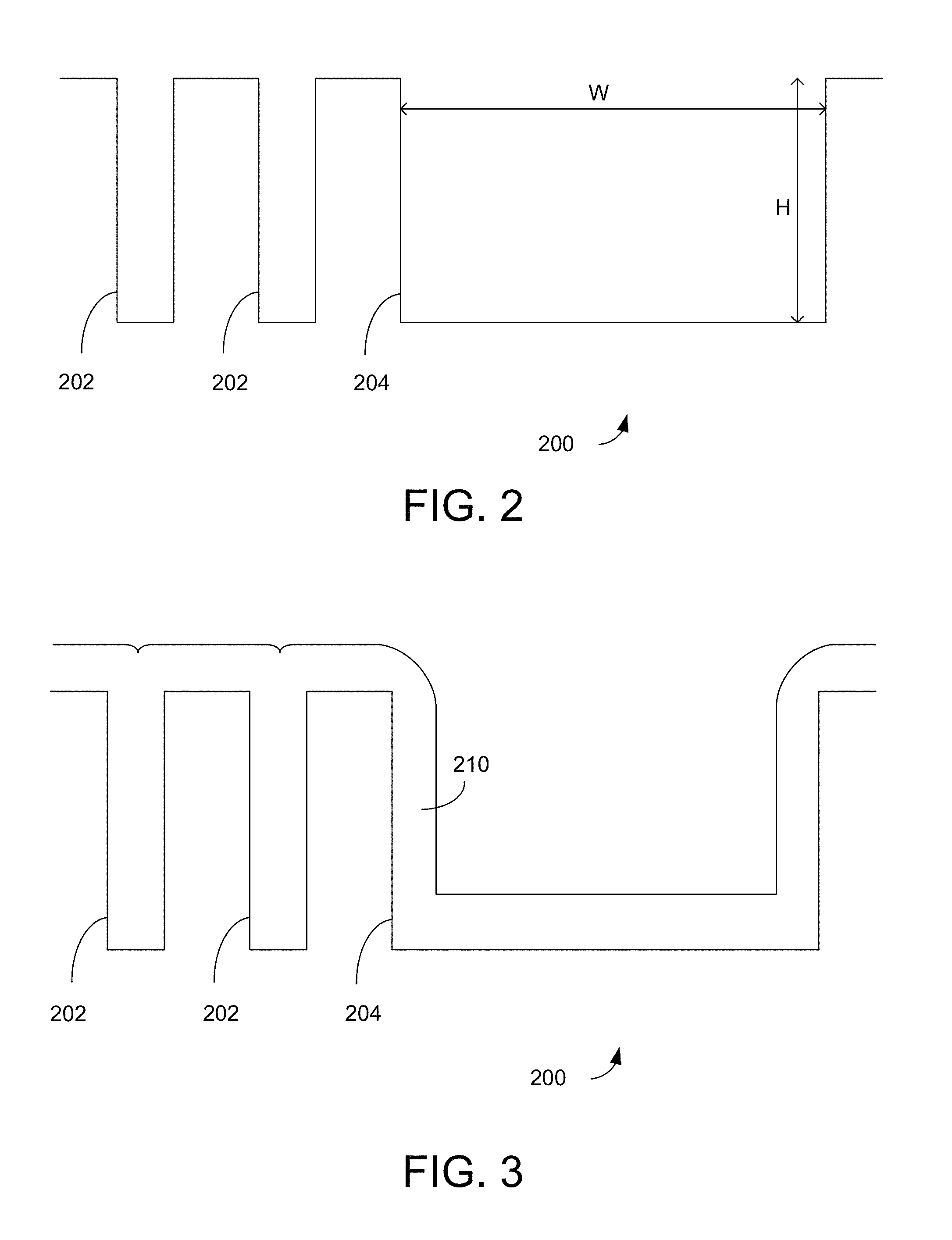
FIG. 2 shows a substrate having gaps of different aspect ratios that may be filled according to the disclosed embodiments.
FIG. 3 shows the substrate of FIG. 2 after a PEALD deposition process is performed.
FIG. 4 shows a close-up view of a narrow gap of FIGS. 2 and 3 as the PEALD process is performed to fill the gap.
FIG. 5 shows a flowchart of a method of depositing a film through a plasma enhanced chemical vapor deposition (PECVD) process.
FIG. 6 shows a block diagram of an apparatus that may be used to carry out the disclosed methods.
FIG. 7 depicts a multi-station apparatus that may be used to carry out the disclosed methods.
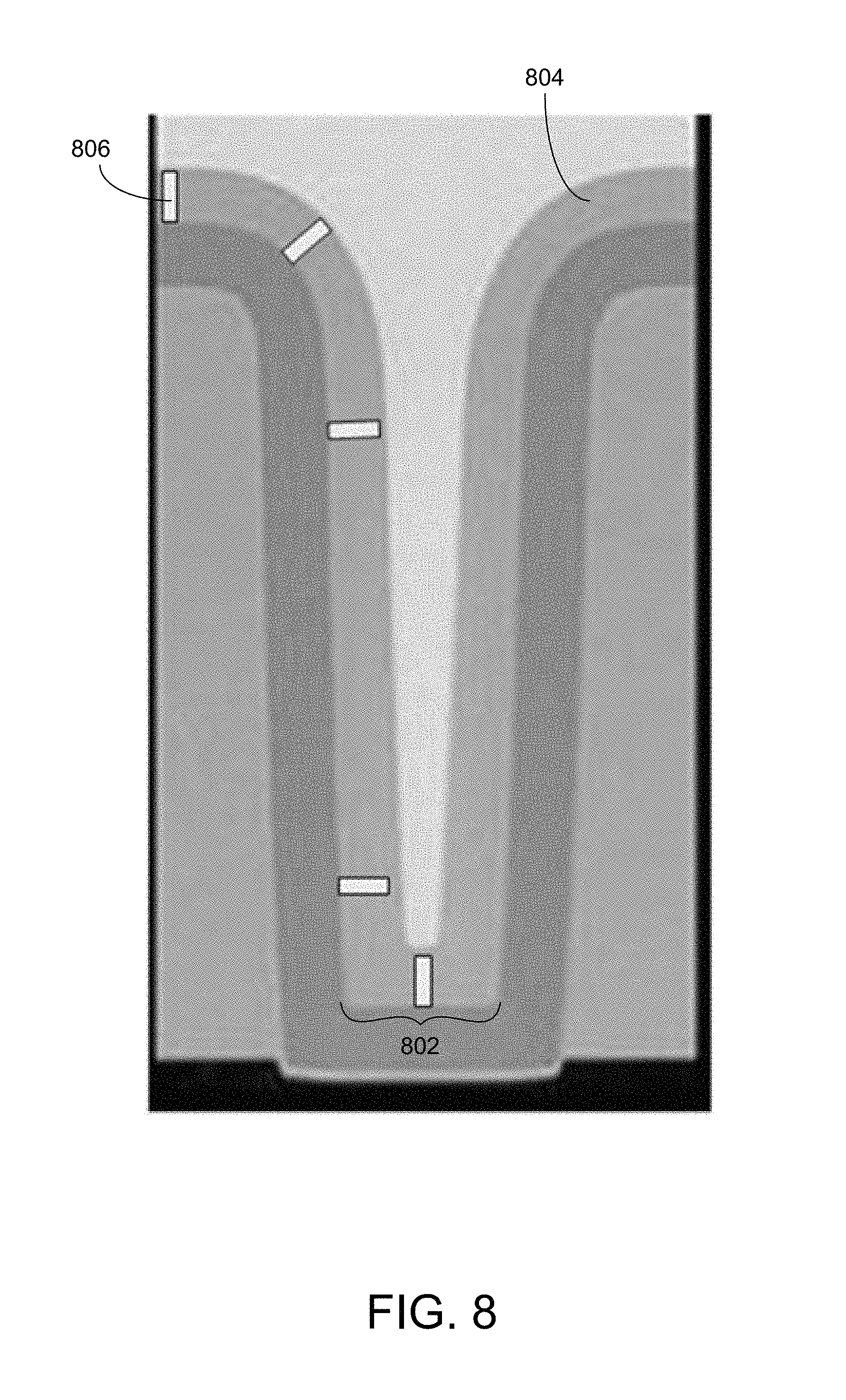
FIG. 8 shows a partially filled high aspect ratio gap that was filled according to the disclosed PEALD methods.
FIGS. 9-11 show additional pictures of high aspect ratio gaps filled according to the disclosed PEALD methods.
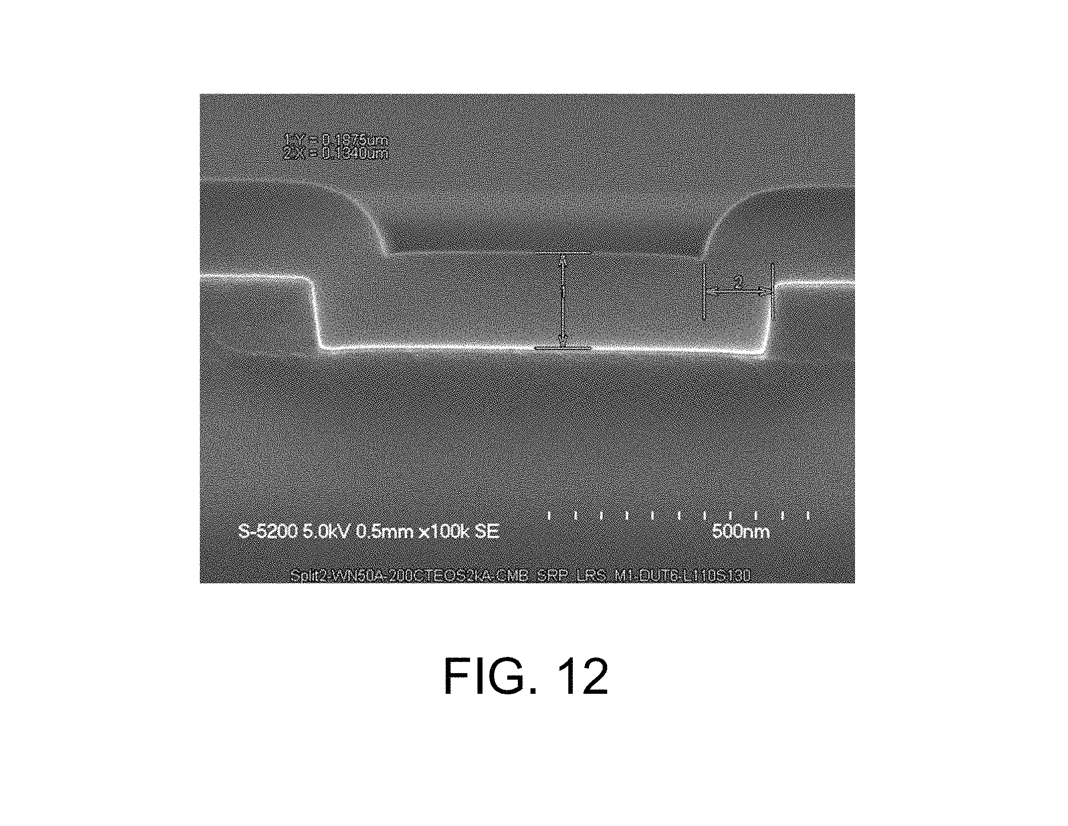
FIG. 12 shows a wide gap filled with silicon oxide deposited according to a disclosed PECVD method.
DETAILED DESCRIPTION
In this application, the terms "semiconductor wafer," "wafer," "substrate," "wafer substrate," and "partially fabricated integrated circuit" are used interchangeably. One of ordinary skill in the art would understand that the term "partially fabricated integrated circuit" can refer to a silicon wafer during any of many stages of integrated circuit fabrication thereon. A wafer or substrate used in the semiconductor device industry may have a diameter of 200 mm, or 300 mm, or 450 mm. The following detailed description assumes the invention is implemented on a wafer. However, the invention is not so limited. The work piece may be of various shapes, sizes, and materials. In addition to semiconductor wafers, other work pieces that may take advantage of this invention include various articles such as printed circuit boards, glass panels, and the like.
In the following description, numerous specific details are set forth in order to provide a thorough understanding of the presented embodiments. The disclosed embodiments may be practiced without some or all of these specific details. In other instances, well-known process operations have not been described in detail to not unnecessarily obscure the disclosed embodiments. While the disclosed embodiments will be described in conjunction with the specific embodiments, it will be understood that it is not intended to limit the disclosed embodiments.
Conventional gap fill techniques have been unsuccessful in achieving void-free, seam-free fill for high density films in high aspect ratio gaps. HDP, SACVD and LPCVD have only limited fill capability, and typically result in the formation of voids and seams. These voids and seams can open up after a chemical mechanical polishing (CMP) operation, or after an etch-back is performed. These opened seams and voids can then trap materials, such as polysilicon and tungsten, that are subsequently deposited. These materials are often incompletely removed in subsequent CMP or etch-back operations, and can remain in the device to cause shorts and/or loss of yield. Flowable CVD (e.g., flowable oxide) and SOD techniques have complex integration schemes that may result in high costs associated with the various additional steps involved.
Certain embodiments herein relate to a hybrid method of filling differently sized gaps on a semiconductor substrate. The first portion of the method relates to an ALD operation, for example a plasma enhanced ALD (PEALD) operation. The ALD operation may be performed in a novel way to promote a bottom-up type fill in narrow gaps. This bottom-up fill mechanism helps achieve the void-free, seam-free fill, particularly in narrow gaps (e.g., gaps having a critical dimension (CD) of about 50 nm or less) and/or gaps having high aspect ratios (e.g., depth to width aspect ratio of about 4:1 or higher). The ALD operation also acts to form a layer on, but not completely fill, wider gaps present on the substrate (e.g., gaps having a CD larger than about 50 nm) having lower aspect ratios (e.g., aspect ratios of about 4:1 or lower).
The second portion of the method relates to a plasma enhanced chemical vapor deposition (PECVD) method that is used to fill the remainder of the wider gaps. In certain embodiments, this method may be performed using a direct (in situ) capacitively coupled plasma. In many embodiments, a radio frequency (RF) plasma source is employed, though any type of plasma source capable of generating a direct plasma may be employed, including microwave and DC sources. Further, in some embodiments, a remotely-generated plasma may be employed. The remote plasma may be capacitively-coupled or inductively-coupled according to various embodiments.
The plasmas used in the PECVD methods described herein may have lower plasma density than high density plasmas generated by in-situ inductively coupled plasma generators such as those used in HDP processes. For example, in HDP processes plasma densities may be on the order of about 10.sup.11-10.sup.13 ions/cm.sup.3, as opposed to about 10.sup.8-10.sup.10 ions/cm.sup.3 for PECVD processes in certain embodiments. HDP methods generally do not produce the required fill results, as described above, and typically require the use of etch operations between subsequent deposition steps. In HDP methods, charged dielectric precursor species are directed downwards to fill the gap. This results in some sputtering of material, which can then redeposit on the sidewalls of the gap, especially near the top of the gap, as well as in the field region. Further, uncharged particles present in the chamber may deposit in the upper sidewall region, as well. This unwanted deposition can build up to form sidewall deposits and top-hats, which prevent the gap from being uniformly filled. Etch steps may be used to combat the undesired upper sidewall deposition that occurs with HDP, though this increases the complexity of the deposition method. If no etch steps are performed, the gap will generally not be able to fill without formation of a void. The HDP methods are also much more expensive to implement, with a lower throughput than PECVD methods.
According to various embodiments, the PEALD and PECVD methods may be implemented in the same chamber. Both of these types of processes run in similar pressure and flow regimes, and can use the same RF power sources. Further, the PECVD methods may be performed in a single step, meaning that no intervening etching operations (or other processes such as deposition processes) are required. By contrast, it is not practical to run PEALD and HDP processes in the same chamber. First, the two processes operate in substantially different pressure regimes. PEALD processes generally run in the range of a few Torr, and benefit from high gas flows for purging. HDP processes operate in the mTorr range, which requires relatively low gas flows compared to what is used with PEALD. Next, HDP processes are typically practiced in large volume chambers, while ALD processes benefit from substantially smaller volumes. Furthermore, HDP processes generally require a different power source than PEALD, which would further complicate reactor design.
Although HDP processes have shown good gap fill, HDP processes suffer from engineering problems related to "forbidden gap" sizes. Where a hybrid ALD/HDP deposition approach is used, a forbidden gap may exist where the CD of the gap is slightly larger than 2.times. the thickness of the ALD layer deposited. In these cases, the HDP processes are unable to fill the remaining gap. The PECVD methods described herein can fill gaps including those previously lined with PEALD. After any challenging structures are lined/filled with PEALD, the PECVD process may be used to fill remaining structures in a less conformal manner.
The PECVD operation is advantageous in achieving a high deposition rate to fill larger gaps that would take a long time to fill through ALD alone. In some embodiments, however, the methods include only the first operation of performing PEALD.
In various embodiments, the PEALD and PECVD operations are performed in the same chamber. This setup is beneficial, as there is no need to transfer the substrate from a PEALD reaction chamber to a PECVD reaction chamber. Thus, there is no need to worry about moisture getting on or into the film, and there is no corresponding need to perform a de-gassing operation or high temperature anneal to remove the moisture before performing the PECVD operation. Another benefit to the single chamber approach is that it reduces capital costs, cycle times and process flow complexity.
Variations may be made to the basic method described above to achieve different hybrid filling scenarios. In one example, a first portion of the method includes a PEALD operation performed under optimum conditions for filling a high aspect ratio gap, and a second portion of the method includes a more relaxed PEALD operation such as one having reduced dose and purge times. These relaxed PEALD operations may also promote PECVD or partial PECVD deposition. In another example, an etch step is used to taper the gap profile. The etch step may be performed between a first portion of the method and a second portion of the method (e.g., between a PEALD operation and a PECVD operation), or within a single portion of the method (e.g., between two PEALD operations or between two PECVD operations). Of course, the methods may be combined as appropriate. The optimum solution will depend on the actual distribution of aspect ratios and gap dimensions present on the substrate.
Combined PEALD and PECVD methods for filling gaps on substrates are discussed in U.S. patent application Ser. No. 13/084,399, which was incorporated by reference above. In certain cases, as discussed in Ser. No. 13/084,399, there may be a transition phase between an PEALD operation and a PECVD operation in which both PEALD surface reactions and PECVD gas phase reactions occur simultaneously.
In such embodiments, the completed film is generated in part by ALD/CFD and in part by a CVD process such as PECVD. Typically, the ALD/CFD portion of the deposition process is performed first and the PECVD portion is performed second, although this need not be the case. Mixed ALD/CFD with CVD processes can improve the step coverage over that seen with CVD alone and additionally improve the deposition rate over that seen with ALD/CFD alone. In some cases, plasma or other activation is applied while one ALD/CFD reactant is flowing in order to produce parasitic CVD operations and thereby achieve higher deposition rates, a different class of films, etc.
In certain embodiments, two or more ALD/CFD phases may be employed and/or two or more CVD phases may be employed. For example, an initial portion of the film may be deposited by ALD/CFD, followed by an intermediate portion of the film being deposited by CVD, and a final portion of the film deposited by ALD/CFD. In such embodiments, it may be desirable to modify the CVD portion of the film, as by plasma treatment or etching, prior to depositing the later portion of the film by ALD/CFD.
A transition phase may be employed between the ALD/CFD and CVD phases. The conditions employed during such transition phase different from those employed in either the ALD/CFD or the CVD phases. Typically, though not necessarily, the conditions permit simultaneous ALD/CFD surface reactions and CVD type gas phase reactions. The transition phase typically involves exposure to a plasma, which may be pulsed for example. Further, the transition phase may involve delivery of one or more reactants at a low flow rate, i.e., a rate that is significantly lower than that employed in the corresponding ALD/CFD phase of the process.
Methods
Plasma Enhanced Atomic Layer Deposition
The disclosed PEALD processes are useful in achieving void-free, seam-free fill of relatively narrow/high aspect ratio features. Unexpectedly, certain embodiments of the processes appear to result in a bottom-up fill mechanism where material is preferentially deposited near the bottom of the gap as opposed to the top of the gap as the gap is being filled. Although deposition happens on the sidewalls and field region as well, the film deposits thicker at/near the bottom of the gap and in many cases achieves a tapered profile as the gap is filled. The tapered profile is defined to mean that the film deposits thicker near the bottom and thinner near the top of the gap, as shown in the Experimental section, below. This tapered profile is especially useful in achieving a high quality fill without voids or seams in high aspect ratio features. This fill mechanism was unexpected, as atomic layer deposition methods typically result in the formation of a seam as the sidewalls close in towards one another. By promoting bottom-up fill, this seam can be avoided and a more robust device results.
Without wishing to be bound by any theory or mechanism of action, it is believed that the bottom-up fill mechanism may be caused by preferential film densification near the top of the gap. As the film is exposed to plasma, species present in the plasma (especially ions) bombard the film surface, thereby compacting and densifying the film. Under appropriate conditions, this densification may happen preferentially near the top of the gap. Due to the shape of the gap, it is much easier for ions to bombard the film in the field region and near the top of the gap, as opposed to near the bottom of the gap, which is much more protected. Thus, the film near the top becomes denser and thinner than the material near the bottom of the trench, which remains thicker and less dense.
Another factor that may promote seam-free, void-free, bottom-up filling is that crosslinking may occur between groups present on opposing sidewalls of the gap. As deposition proceeds and the sidewalls close in towards one another, the terminal groups may crosslink with one another, thus avoiding any seam. In the case of a gap-filling silicon oxide film, for example, surface hydroxyls/silanols on one sidewall may crosslink with surface hydroxyls/silanols on the opposing wall, thereby liberating water and forming a silicon-oxide matrix. These terminal cross-linking groups may preferentially be found on the sidewalls of a gap.
A further factor that may promote seam-free, void-free, bottom-up filling is that ligand byproducts may be liberated from the film in a non-uniform manner, such that the byproducts become preferentially trapped at or near the bottom of the gap as opposed to near the top of the gap. This entrapment may lead to a higher deposition rate within the feature, especially near the bottom of the gap. For example, where bis(tertiary-butyl-amino)silane (BTBAS) is used as a precursor, one type of ligand byproduct that may become entrapped is tert-butylamine (TBA). It is understood, however, that where ligands become trapped in a growing film, the properties of the film may be affected to some degree.
FIG. 1 presents a flowchart for a method of performing a plasma enhanced atomic layer deposition process 100. The process 100 begins at operation 101, where a dose of a first reactant is provided to a reaction chamber containing a substrate. The substrate will typically have gaps therein that are to be filled, partially or completely, through the PEALD process. In one embodiment, the PEALD process 100 completely fills gaps of a first type, and partially fills (e.g., lines) gaps of a second type, as discussed further below. In various cases, the first reactant may be a silicon-containing reactant. Next, at operation 103 the reaction chamber is purged, for example with an inert gas or a nitrogen carrier gas. This helps remove any remaining first reactant from the reaction chamber.
At operation 105, the second reactant is provided to the reaction chamber. In certain cases, the second reactant is an oxidizing reactant. The second reactant may also be a mix of reactants. In a particular embodiment, the second reactant is a roughly equal volume flow of oxygen and nitrous oxide. As used herein, the phrase "roughly equal volume flow" means that the flow of a first species and the flow of a second species do not differ by more than about 20%, as measured in SLM. The second reactant is provided in operation 105, which may include pre-flowing the reactant before flowing the reactant coincident with plasma activation in operation 107. When the plasma is activated, it drives a reaction between the first and second reactants on the surface of the substrate. Next, the plasma is extinguished, and then the reaction chamber is purged, for example with inert gas or a nitrogen carrier gas. This operation 109 is referred to as the post-RF purge.
The method 100 is typically repeated a number of times to build up the desired film thickness. By using the conditions and methods disclosed herein, the method 100 can result in a fill having a tapered profile and bottom-up fill characteristics. These factors promote void-free, seam-free fill. Advantageously, the film deposited through the disclosed methods are fairly dense.
In a particular example, operation 101 includes providing BTBAS (or other primary reactant) at a flow rate of about 0.5-2.5 mL/min, or about 1.5-2.5 L/min, for example 2 mL/min, for a time period of between about 0.1-1 second, or about 0.2-0.5 seconds, for example about 0.3 seconds. Operation 103 includes purging the reaction chamber with inert gas for between about 0.1-1 seconds, or between about 0.2-0.5 seconds, for example about 0.3 seconds. Operation 105 includes co-flowing O.sub.2 and N.sub.2O at a flow rate between about 2-20 SLM each, or between about 8-12 SLM each, for example about 10 SLM each. Coincident with this reactant delivery, a plasma is generated at operation 107 using between about 300 W-10 kW, or between about 4-6 kW, for example about 5 kW RF power. These values represent the total RF power delivered, which is divided among four stations/pedestals. The plasma exposure lasts for a duration between about 10 milliseconds and 3 seconds, or between about 0.25-1 second, for example about 0.5 seconds. The RF frequency applied to generate the plasma may be about 13.56 or 27 MHz. Next, the reaction chamber is purged with inert gas at operation 109 for a time period between about 10 milliseconds and 5 seconds, or between about 50-150 milliseconds, for example about 90 milliseconds. It should be understood that the above conditions are examples, with other reactants, flow rates, pulse times, and power used as appropriate for the particular implementation.
The PEALD methods described herein may be conformal film deposition (CFD) methods. Plasma enhanced conformal film deposition techniques and apparatus are further discussed and described in U.S. patent application Ser. No. 13/084,399, filed Apr. 11, 2011, and titled "PLASMA ACTIVATED CONFORMAL FILM DEPOSITION," which is incorporated by reference in its entirety above.
PEALD Reactants
The disclosed methods and apparatus are not limited to use with particular precursors. While the methods have already proven to be effective with certain precursors (as shown in the Experimental section) it is believed that the methods may also be used with a variety of other precursors to gain similar benefits.
At least one of the reactants will generally contain an element that is solid at room temperature, the element being incorporated into the film formed by the PEALD/PECVD method. This reactant may be referred to as a principal reactant. The principal reactant typically includes, for example, a metal (e.g., aluminum, titanium, etc.), a semiconductor (e.g., silicon, germanium, etc.), and/or a non-metal or metalloid (e.g., boron). The other reactant is sometimes referred to as an auxiliary reactant or a co-reactant. Non-limiting examples of co-reactants include oxygen, ozone, hydrogen, hydrazine, water, carbon monoxide, nitrous oxide, ammonia, alkyl amines, and the like. The co-reactant may also be a mix of reactants, as mentioned above.
The PEALD/PECVD process may be used to deposit a wide variety of film types and in particular implementations to fill gaps with these film types. While much of the discussion herein focuses on the formation of undoped silicon oxides, other film types such as nitrides, carbides, oxynitrides, carbon-doped oxides, nitrogen-doped oxides, borides, etc. may also be formed. Oxides include a wide range of materials including undoped silicate glass (USG), doped silicate glass. Examples of doped glasses included boron doped silicate glass (BSG), phosphorus doped silicate glass (PSG), and boron phosphorus doped silicate glass (BPSG). Still further, the PEALD/PECVD process may be used for metal deposition and feature fill.
While the disclosed embodiments are not limited to particular reactants, an exemplary list of reactants is provided below.
In certain embodiments, the deposited film is a silicon-containing film. In these cases, the silicon-containing reactant may be for example, a silane, a halosilane or an aminosilane. A silane contains hydrogen and/or carbon groups, but does not contain a halogen. Examples of silanes are silane (SiH.sub.4), disilane (Si.sub.2H.sub.6), and organo silanes such as methylsilane, ethylsilane, isopropylsilane, t-butylsilane, dimethylsilane, diethylsilane, di-t-butyl silane, allylsilane, sec-butyl silane, thexylsilane, isoamylsilane, t-butyldisilane, di-t-butyldisilane, tetra-ethyl-ortho-silicate (also known as tetra-ethoxy-silane or TEOS) and the like. A halosilane contains at least one halogen group and may or may not contain hydrogens and/or carbon groups. Examples of halosilanes are iodosilanes, bromosilanes, chlorosilanes and fluorosilanes. Although halosilanes, particularly fluorosilanes, may form reactive halide species that can etch silicon materials, in certain embodiments described herein, the silicon-containing reactant is not present when a plasma is struck. Specific chlorosilanes are tetrachlorosilane (SiCl.sub.4), trichlorosilane (HSiCl.sub.3), dichlorosilane (H.sub.2SiCl.sub.2), monochlorosilane (ClSiH.sub.3), chloroallylsilane, chloromethylsilane, dichloromethyl silane, chlorodimethylsilane, chloroethylsilane, t-butylchlorosilane, di-t-butylchlorosilane, chloroisopropylsilane, chloro-sec-butylsilane, t-butyldimethylchlorosilane, thexyldimethylchlorosilane, and the like. An aminosilane includes at least one nitrogen atom bonded to a silicon atom, but may also contain hydrogens, oxygens, halogens and carbons. Examples of aminosilanes are mono-, di-, tri- and tetra-aminosilane (H.sub.3Si(NH.sub.2).sub.4, H.sub.2Si(NH.sub.2).sub.2, HSi(NH.sub.2).sub.3 and Si(NH.sub.2).sub.4, respectively), as well as substituted mono-, di-, tri- and tetra-aminosilanes, for example, t-butylaminosilane, methylaminosilane, tert-butylsilanamine, bis(tertiarybutylamino)silane (SiH.sub.2(NHC(CH.sub.3).sub.3).sub.2 (BTBAS), tert-butyl silylcarbamate, SiH(CH.sub.3)--(N(CH.sub.3).sub.2).sub.2, SiHCl--(N(CH.sub.3).sub.2).sub.2, (Si(CH.sub.3).sub.2NH).sub.3 and the like. A further example of an aminosilane is trisilylamine (N(SiH.sub.3)).
In other cases, the deposited film contains metal. Examples of metal-containing films that may be formed include oxides and nitrides of aluminum, titanium, hafnium, tantalum, tungsten, manganese, magnesium, strontium, etc., as well as elemental metal films. Example precursors may include metal alkylamines, metal alkoxides, metal alkylamides, metal halides, metal -diketonates, metal carbonyls, organometallics, etc. Appropriate metal-containing precursors will include the metal that is desired to be incorporated into the film. For example, a tantalum-containing layer may be deposited by reacting pentakis(dimethylamido)tantalum with ammonia or another reducing agent. Further examples of metal-containing precursors that may be employed include trimethylaluminum, tetraethoxytitanium, tetrakis-dimethyl-amido titanium, hafnium tetrakis(ethylmethylamide), bis(cyclopentadienyl)manganese, bis(n-propyl cyclopentadienyl)magnesium, etc.
In certain implementations, an oxygen-containing oxidizing reactant is used. Examples of oxygen-containing oxidizing reactants include oxygen, ozone, nitrous oxide, carbon monoxide, etc.
In some embodiments, the deposited film contains nitrogen, and a nitrogen-containing reactant is used. A nitrogen-containing reactant contains at least one nitrogen, for example, ammonia, hydrazine, amines (e.g., amines bearing carbon) such as methylamine, dimethylamine, ethylamine, isopropylamine, t-butylamine, di-t-butylamine, cyclopropylamine, sec-butylamine, cyclobutylamine, isoamylamine, 2-methylbutan-2-amine, trimethylamine, diisopropylamine, diethylisopropylamine, di-t-butylhydrazine, as well as aromatic containing amines such as anilines, pyridines, and benzylamines. Amines may be primary, secondary, tertiary or quaternary (for example, tetraalkylammonium compounds). A nitrogen-containing reactant can contain heteroatoms other than nitrogen, for example, hydroxylamine, t-butyloxycarbonyl amine and N-t-butyl hydroxylamine are nitrogen-containing reactants.
Other precursors, such as will be apparent to or readily discernible by those skilled in the art given the teachings provided herein, may also be used.
Gap Conditions
The disclosed PEALD process is especially useful for filling relatively narrow gaps (CD< about 50 nm) having a relatively high aspect ratio (AR> about 4:1). However, the process may also be performed on larger gaps and gaps having smaller ARs, as well.
In various embodiments, the PEALD process is performed on a substrate having at least two different types of gaps. A first type may include gaps having a CD less than about 50 nm, and/or an AR greater than about 4:1. This first type is referred to as a narrow gap. A second type may include gaps having a CD greater than about 50 nm, and/or an AR less than about 4:1. This second type is referred to as a wide gap. For the reasons discussed above, it can be difficult to simultaneously fill both narrow and wide gaps. Another way to characterize the different types of gaps is by comparing their sizes relative to one another. In some cases, a wide gap is at least about 2 times, or at least about 5 times, or at least about 10 times wider than a narrow gap. In these or other cases, the AR of the narrow gap may be at least about 2 times, or at least about 5 times, or at least about 10 times greater than the AR of the wide gap.
In many implementations where the PEALD process is performed on a substrate having both narrow and wide gaps, the PEALD process will act to completely fill the narrow gap, and line the surface of the wide gap. FIG. 2 presents a substrate 200 having two different types of gaps 202 and 204. The aspect ratio of the gaps is calculated as the height of the gap divided by the width of the gap. These dimensions are labeled in FIG. 2. Gaps 202 are narrow gaps having an aspect ratio slightly larger than 4:1. Gaps 204 are wide gaps having an aspect ratio of about 1:2.
FIG. 3 shows the same substrate 200 after a PEALD deposition process is performed to deposit an oxide layer 210. The narrow gaps 202 are completely filled, while the wide gap 204 is lined with oxide material 210. The film 210 deposited on the bottom of the wide gap 204 may be slightly thicker than the film 210 deposited on the sidewalls of gap 204. However, this thickness difference is much more pronounced in the narrow gap 202 as it fills with material.
FIG. 4 shows a portion of substrate 200 at a time during the PEALD deposition process. In particular, narrow gap 202 is shown mid-deposition. The deposited oxide layer 210 has a tapered profile, such that the film is thinner near the top of the gap and thicker near the bottom of the gap. This results in a diminishing gap that is smaller at the bottom than at the top. This shape is ideal for promoting void-free, seam-free fill. As material fills into the bottom of the gap, the mechanisms described above (e.g., preferential film densification, preferential ligand trapping, and/or crosslinking) may act to fill the feature without any voids or seams. Experimental results demonstrating such a fill mechanism are included below in the Experimental section.
This fill mechanism has not been previously observed with PEALD type processes. Instead, conventional PEALD processes form films that have no such tapered profile, where more vertical sidewalls grow towards one another and meet in the center. In these conventional methods, chemicals may get trapped in the extremely narrow void/seam formed in the center of the gap. This trapping is likely to occur, in part because the entire height of the gap closes in at substantially the same time. Conversely, with the disclosed methods, the sidewalls close in towards each other to a greater degree towards the bottom of the gap as opposed to the top of the gap. Thus, as the sidewalls grow towards one another, the bottom of the deposited film grows upwards, and chemicals present in the gap are pushed out. This results in a process where seam and void formation is avoided, producing an excellent quality filled gap.
In some embodiments, a gap filled by a PEALD operation has a reentrant profile. In other words, the gap is smaller at an upper portion and wider at a lower portion. It has been observed that bottom-up fill can be achieved with the disclosed PEALD process, even with gaps that have a somewhat reentrant profile. These results are shown below in the Experimental section.
Chamber Conditions
The PEALD process has been shown to be fairly resilient to changes in temperature. In particular, the process has been shown to be effective at 200.degree. C. and 400.degree. C. In some embodiments, therefore, the process is conducted at a temperature between about 200-400.degree. C. In other cases, however, the temperature may fall outside this range.
The pressure inside the reaction chamber during the PEALD process may be between about 1-10 Torr, or between about 3-7 Torr, for example about 6 Torr.
Plasma Generation Conditions
In the PEALD operation, the substrate is exposed to plasma to drive the reaction between the first and second reactants. Various types of plasma may be used to drive this reaction including capacitively coupled plasmas and inductively coupled plasmas. Various types of plasma generators may be used including RF, DC, and microwave plasma generators. Moreover, according to various embodiments, the plasma may be direct or remote.
The gas used to generate the plasma may include an inert gas such as argon or helium. The gas will also typically include one of the reactants, for example an oxidizing reactant where an oxide film is being formed.
In many cases, an RF signal is used to drive plasma formation. In some embodiments, the RF applied is high frequency RF only, for example at a frequency of about 13.56 or 27 MHz. In other embodiments, the RF has a low frequency component as well. The RF power delivered to drive plasma formation may be between about 300 W and about 10 kW. In some cases, the RF power delivered is between about 4-6 kW, for example about 5 kW. These values represent the total power delivered, which is divided among four stations/pedestals.
Additional plasma generation conditions are discussed in U.S. patent application Ser. No. 13/084,399, filed Apr. 11, 2011, and titled "PLASMA ACTIVATED CONFORMAL FILM DEPOSITION," which is incorporated by reference above.
The duration of plasma exposure may vary between different embodiments. In some cases, RF power is applied for between about 10 milliseconds and 3 seconds, or between about 0.25 seconds and about 1 second. In a particular example, RF power is applied for about 0.5 seconds. The RF power and RF time determine the RF flux delivered to the chamber. It has been found that by increasing the RF flux (either by increasing RF time or power), the wet etch rate (WER) of the film may be reduced. Because the PEALD process has shown a fair resilience to different RF conditions, these variables may be used to achieve a tunable WER.
Purge Conditions
Generally, two sweep/purge operations occur during a single cycle of a PEALD reaction. The first purge occurs after the dose of the first reactant is delivered to the processing chamber, and may be referred to as a reactant purge. This purge is conducted to sweep out any remaining, non-adsorbed first reactant. The second purge occurs after the substrate is exposed to plasma, and may be referred to as the post-RF purge. This purge is conducted to sweep out any remaining reactants, as well as any film formation byproducts.
There are various ways to purge a reaction chamber. One method involves supplying the chamber with a flow of non-reactant gas (e.g., argon, helium, nitrogen, etc.) to sweep out any undesired species. With a sweep, the pressure in the reaction chamber stays substantially constant. Another method of purging a reaction chamber is to perform a pump down. Where this is the case, a vacuum is applied and the reaction chamber is evacuated. During the evacuation, the pressure in the reaction chamber is significantly reduced, for example to less than about 1 Torr.
It has been found that gapfill results are better where the post-RF purge includes a sweep, as compared to a pump down. Without wishing to be bound by a particular theory or mechanism of action, it is believed that the post-RF conditions, including the presence or absence of a pump down, may affect the surface functionality present on the surface of the deposited film. This surface functionality may determine whether or not crosslinking occurs between opposing sidewalls as the gap is filled. One way to encourage the desired bottom-up deposition pattern is to sweep the reaction chamber instead of performing a pump down. Thus, in certain embodiments, no pump down is performed after plasma exposure during the PEALD deposition. In some cases, however, a pump down may be performed between a PEALD operation and a PECVD operation.
The reactant purge may be performed for a duration between about 0.1-1 seconds, for example between about 0.2-0.5 seconds. In a particular example, the reactant purge has a duration of about 0.3 seconds.
The post-RF purge may be performed for a duration between about 0.01-5 seconds, for example between about 0.05-0.15 seconds. In one case the post-RF purge has a duration of about 0.09 seconds.
Plasma Enhanced Chemical Vapor Deposition
The PECVD methods disclosed herein may be practiced after a PEALD process to finish filling gaps that were only partially filled/lined. This method is advantageous compared to a PEALD process alone because it offers a much higher deposition rate, resulting in decreased processing times and increased throughput. Thus, the PEALD process may be used to fill small gaps and line large gaps, and then the PECVD process may be used to complete the filling of the large gaps. This offers a convenient way to fill features of varying sizes and aspect ratios. In many cases, the gaps can be filled without any intervening etching operations.
In a PECVD reaction, a substrate is exposed to one or more volatile precursors, which react and/or decompose to produce the desired deposit on the substrate surface. FIG. 5 shows a flow chart for a method 500 of filling a gap with PECVD. In various embodiments, the method 500 may be performed after the method 100 of FIG. 1. The PECVD method generally begins by flowing one or more reactants into the reaction chamber at operation 501. The reactant delivery may continue as plasma is generated in operation 503. The substrate surface is exposed to plasma, which causes deposition to occur on the substrate surface in operation 505. This process continues until a desired film thickness is reached. At operation 507, the plasma is extinguished and the reactant flow is terminated. Next, the reaction chamber is purged at operation 509.
In one example process, operation 501 includes flowing TEOS at a rate of about 1-20 mL/min and O.sub.2 at a rate of about 2,000-30,000 sccm. RF power is applied with an HF component between about 200-3,000 W, and an LF component between about 200-2,500 W (divided among four stations). The HF frequency is about 13.56 or 27 MHz, while the LF frequency is between about 300-400 kHz. The pressure in the reaction chamber is between about 1-10 Torr, and the temperature is between about 100-450.degree. C. Of course, it is understood that in other embodiments, the reactants, chamber conditions, timing, etc. may vary depending on the desired film and application. The values provided in this section are not intended to be limiting.
PECVD methods and apparatus are further discussed and described in the following patent documents, which are each herein incorporated by reference in their entireties: U.S. Pat. No. 7,381,644, titled "PULSED PECVD METHOD FOR MODULATING HYDROGEN CONTENT IN HARD MASK"; U.S. Pat. No. 8,110,493, titled "PULSED PECVD METHOD FOR MODULATING HYDROGEN CONTENT IN HARD MASK"; U.S. Pat. No. 7,923,376, titled "METHODS OF REDUCING DEFECTS IN PECVD TEOS FILMS"; and U.S. patent application Ser. No. 13/478,999, titled "PECVD DEPOSITION OF SMOOTH SILICON FILMS," filed May 23, 2012.
In many cases, there will be no downtime between a PEALD process and a PECVD process. For example, the PEALD process may end by extinguishing the plasma, performing the post-RF purge (with or without a pump down), and then immediately flowing the PECVD reactant(s).
In some embodiments, hybrid PEALD/PECVD methods as discussed and described in U.S. patent application Ser. No. 13/084,399, filed Apr. 11, 2011, and titled "PLASMA ACTIVATED CONFORMAL FILM DEPOSITION," which is incorporated by reference above, may be used.
PECVD Reactants
The PECVD reaction may be performed with either the same reactants as the ALD reaction, or with different reactants. In one embodiment, the PEALD reaction is performed with BTBAS and a mixture of O.sub.2/N.sub.2O, and the PECVD reaction is performed with TEOS and/or silane. The TEOS and silane reactants have been found to be especially useful in practicing the PECVD reaction. Generally, the reactants listed above in the PEALD Reactants section may be used in the PECVD reaction.
The flow rate of reactants may vary depending on the desired process. In one embodiment related to PECVD undoped silicate glass (USG), SiH.sub.4 is used as a reactant and has a flow rate between about 100-1,500 sccm, with a flow of N.sub.2O between about 2,000-20,000 sccm. In another embodiment related to PECVD using TEOS, the flow of TEOS is between about 1-20 mL/min, and the flow of O.sub.2 is between about 2,000-30,000 sccm.
Chamber Conditions
The temperature in the reaction chamber during the PECVD reaction may be between about 50-450.degree. C., in certain embodiments. This range may be especially appropriate for reactions using silane. Where other reactants are used, the temperature range may be more limited or more broad, for example between about 100-450.degree. C. where TEOS is used.
The pressure in the reaction chamber during the PECVD reaction may be between about 1-10 Torr, for example about 5 Torr.
Because the chamber conditions are very similar between the PEALD operation and the PECVD operation, it is feasible to implement both types of reactions in a single reaction chamber. As discussed above, this is advantageous because it reduces or eliminates the risk of moisture entering the film as the substrate is moved between processing chambers, and reduces the need to perform a degassing operation between the two processes.
Plasma Generation Conditions
The PECVD reactions are driven by exposure to plasma. The plasma may be a capacitively coupled plasma or a remotely generated inductively coupled plasma. For the reasons discussed above, it may be preferable to avoid using an in situ inductively coupled plasma.
The gas used to generate the plasma will include at least one reactant. The plasma generation gas may also include other species, as well. For example, in certain embodiments the plasma generation gas includes an inert gas.
The frequency used to drive plasma formation may contain both LF and HF components. In some embodiments the HF frequency may be about 13.56 MHz or about 27 MHz. The LF frequency may be between about 300-400 kHz. The HF RF power used to drive plasma formation may be between about 200-3,000 W. The LF RF power used to drive plasma formation may be between about 200-2,500 W. These power levels represent the total power delivered, which is divided among four stations. The duration of plasma exposure depends on the desired thickness of the deposited film.
In some embodiments, pulsed PECVD methods may be used. These methods may involve pulsing precursor and/or RF power levels.
Purge Conditions
A purge is typically conducted after the PECVD deposition is complete. This purge operates to remove reactants and any byproducts from the reaction chamber. Because the film is already deposited at this point, the purge conditions are less important than with the PEALD reactions, which require many iterations of reactant purge and post-RF purge as the PEALD film is formed.
Apparatus
A suitable apparatus for performing the disclosed methods typically includes hardware for accomplishing the process operations and a system controller having instructions for controlling process operations in accordance with the present invention. For example, in some embodiments, the hardware may include one or more PEALD, PECVD or joint PEALD/PECVD process stations included in a process tool.
FIG. 6 provides a block diagram of an example apparatus that may be used to practice the disclosed embodiments. As shown, a reactor 600 includes a process chamber 624, which encloses other components of the reactor and serves to contain the plasma generated by, e.g., a capacitor type system including a showerhead 614 working in conjunction with a grounded heater block 620. A high-frequency RF generator 602, connected to a matching network 606, and a low-frequency RF generator 604 are connected to showerhead 614. The power and frequency supplied by matching network 606 is sufficient to generate a plasma from the process gas, for example 400-700 W total energy. In one implementation of the present invention both the HFRF generator and the LFRF generator are used. In a typical process, the high frequency RF component is generally between about 2-60 MHz; in a preferred embodiment, the HF component is about 13.56 MHz or 27 MHz. The low frequency LF component is generally between about 250-400 kHz; in a particular embodiment, the LF component is about 350 kHz.
Within the reactor, a wafer pedestal 618 supports a substrate 616. The pedestal typically includes a chuck, a fork, or lift pins to hold and transfer the substrate during and between the deposition and/or plasma treatment reactions. The chuck may be an electrostatic chuck, a mechanical chuck or various other types of chuck as are available for use in the industry and/or research.
The process gases are introduced via inlet 612. Multiple source gas lines 610 are connected to manifold 608. The gases may be premixed or not. Appropriate valving and mass flow control mechanisms are employed to ensure that the correct gases are delivered during the deposition and plasma treatment phases of the process. In the case that the chemical precursor(s) are delivered in liquid form, liquid flow control mechanisms are employed. The liquid is then vaporized and mixed with other process gases during its transportation in a manifold heated above its vaporization point before reaching the deposition chamber.
Process gases exit chamber 600 via an outlet 622. A vacuum pump 626 (e.g., a one or two stage mechanical dry pump and/or a turbomolecular pump) typically draws process gases out and maintains a suitably low pressure within the reactor by a close loop controlled flow restriction device, such as a throttle valve or a pendulum valve.
The invention may be implemented on a multi-station or single station tool. In specific embodiments, the 300 mm Novellus Vector.TM. tool having a 4-station deposition scheme or the 200 mm Sequel.TM. tool having a 6-station deposition scheme are used. It is possible to index the wafers after every deposition and/or post-deposition plasma anneal treatment until all the required depositions and treatments are completed, or multiple depositions and treatments can be conducted at a single station before indexing the wafer. It has been shown that film stress is the same in either case. However, conducting multiple depositions/treatments on one station is substantially faster than indexing following each deposition and/or treatment.
FIG. 7 shows a schematic view of an embodiment of a multi-station processing tool 2400 with an inbound load lock 2402 and an outbound load lock 2404, either or both of which may comprise a remote plasma source. A robot 2406, at atmospheric pressure, is configured to move wafers from a cassette loaded through a pod 2408 into inbound load lock 2402 via an atmospheric port 2410. A wafer is placed by the robot 2406 on a pedestal 2412 in the inbound load lock 2402, the atmospheric port 2410 is closed, and the load lock is pumped down. Where the inbound load lock 2402 comprises a remote plasma source, the wafer may be exposed to a remote plasma treatment in the load lock prior to being introduced into a processing chamber 2414. Further, the wafer also may be heated in the inbound load lock 2402 as well, for example, to remove moisture and adsorbed gases. Next, a chamber transport port 2416 to processing chamber 2414 is opened, and another robot (not shown) places the wafer into the reactor on a pedestal of a first station shown in the reactor for processing. While the embodiment depicted in FIG. 4 includes load locks, it will be appreciated that, in some embodiments, direct entry of a wafer into a process station may be provided.
The depicted processing chamber 2414 comprises four process stations, numbered from 1 to 4 in the embodiment shown in FIG. 4. Each station has a heated pedestal (shown at 2418 for station 1), and gas line inlets. It will be appreciated that in some embodiments, each process station may have different or multiple purposes. For example, in some embodiments, a process station may be switchable between a PEALD and PECVD process mode. Additionally or alternatively, in some embodiments, processing chamber 2414 may include one or more matched pairs of PEALD and PECVD process stations. While the depicted processing chamber 2414 comprises four stations, it will be understood that a processing chamber according to the present disclosure may have any suitable number of stations. For example, in some embodiments, a processing chamber may have five or more stations, while in other embodiments a processing chamber may have three or fewer stations.
FIG. 7 also depicts an embodiment of a wafer handling system 2490 for transferring wafers within processing chamber 2414. In some embodiments, wafer handling system 2490 may transfer wafers between various process stations and/or between a process station and a load lock. It will be appreciated that any suitable wafer handling system may be employed. Non-limiting examples include wafer carousels and wafer handling robots. FIG. 7 also depicts an embodiment of a system controller 2450 employed to control process conditions and hardware states of process tool 2400. System controller 2450 may include one or more memory devices 2456, one or more mass storage devices 2454, and one or more processors 2452. Processor 2452 may include a CPU or computer, analog and/or digital input/output connections, stepper motor controller boards, etc.
In some embodiments, system controller 2450 controls all of the activities of process tool 2400. System controller 2450 executes system control software 2458 stored in mass storage device 2454, loaded into memory device 2456, and executed on processor 2452. System control software 2458 may include instructions for controlling the timing, mixture of gases, chamber and/or station pressure, chamber and/or station temperature, purge conditions and timing, wafer temperature, RF power levels, RF frequencies, substrate, pedestal, chuck and/or susceptor position, and other parameters of a particular process performed by process tool 2400. System control software 2458 may be configured in any suitable way. For example, various process tool component subroutines or control objects may be written to control operation of the process tool components necessary to carry out various process tool processes in accordance with the disclosed methods. System control software 2458 may be coded in any suitable computer readable programming language.
In some embodiments, system control software 2458 may include input/output control (IOC) sequencing instructions for controlling the various parameters described above. For example, each phase of a PEALD process may include one or more instructions for execution by system controller 2450. The instructions for setting process conditions for a PEALD process phase may be included in a corresponding PEALD recipe phase. In some embodiments, the PEALD recipe phases may be sequentially arranged, so that all instructions for a PEALD process phase are executed concurrently with that process phase. The same can be said for PECVD processes and hybrid PEALD/PECVD processes.
Other computer software and/or programs stored on mass storage device 2454 and/or memory device 2456 associated with system controller 2450 may be employed in some embodiments. Examples of programs or sections of programs for this purpose include a substrate positioning program, a process gas control program, a pressure control program, a heater control program, and a plasma control program.
A substrate positioning program may include program code for process tool components that are used to load the substrate onto pedestal 2418 and to control the spacing between the substrate and other parts of process tool 2400.
A process gas control program may include code for controlling gas composition and flow rates and optionally for flowing gas into one or more process stations prior to deposition in order to stabilize the pressure in the process station. A pressure control program may include code for controlling the pressure in the process station by regulating, for example, a throttle valve in the exhaust system of the process station, a gas flow into the process station, etc.
A heater control program may include code for controlling the current to a heating unit that is used to heat the substrate. Alternatively, the heater control program may control delivery of a heat transfer gas (such as helium) to the substrate.
A plasma control program may include code for setting RF power levels applied to the process electrodes in one or more process stations.
In some embodiments, there may be a user interface associated with system controller 2450. The user interface may include a display screen, graphical software displays of the apparatus and/or process conditions, and user input devices such as pointing devices, keyboards, touch screens, microphones, etc.
In some embodiments, parameters adjusted by system controller 2450 may relate to process conditions. Non-limiting examples include process gas composition and flow rates, temperature, pressure, plasma conditions (such as RF bias power levels), pressure, temperature, etc. These parameters may be provided to the user in the form of a recipe, which may be entered utilizing the user interface.
Signals for monitoring the process may be provided by analog and/or digital input connections of system controller 2450 from various process tool sensors. The signals for controlling the process may be output on the analog and digital output connections of process tool 2400. Non-limiting examples of process tool sensors that may be monitored include mass flow controllers, pressure sensors (such as manometers), thermocouples, etc. Appropriately programmed feedback and control algorithms may be used with data from these sensors to maintain process conditions.
System controller 2450 may provide program instructions for implementing the above-described deposition processes. The program instructions may control a variety of process parameters, such as DC power level, RF power level, RF bias power level, pressure, temperature, etc. The instructions may control the parameters to operate in-situ deposition of film stacks according to various embodiments described herein.
Lithographic patterning of a film typically comprises some or all of the following steps, each step enabled with a number of possible tools: (1) application of photoresist on a workpiece, e.g., a substrate having a silicon nitride film formed thereon, using a spin-on or spray-on tool; (2) curing of photoresist using a hot plate or furnace or other suitable curing tool; (3) exposing the photoresist to visible or UV or x-ray light with a tool such as a wafer stepper; (4) developing the resist so as to selectively remove resist and thereby pattern it using a tool such as a wet bench or a spray developer; (5) transferring the resist pattern into an underlying film or workpiece by using a dry or plasma-assisted etching tool; and (6) removing the resist using a tool such as an RF or microwave plasma resist stripper. In some embodiments, an ashable hard mask layer (such as an amorphous carbon layer) and another suitable hard mask (such as an antireflective layer) may be deposited prior to applying the photoresist.
It is to be understood that the configurations and/or approaches described herein are exemplary in nature, and that these specific embodiments or examples are not to be considered in a limiting sense, because numerous variations are possible. The specific routines or methods described herein may represent one or more of any number of processing strategies. As such, various acts illustrated may be performed in the sequence illustrated, in other sequences, in parallel, or in some cases omitted. Likewise, the order of the above described processes may be changed.
The subject matter of the present disclosure includes all novel and nonobvious combinations and sub-combinations of the various processes, systems and configurations, and other features, functions, acts, and/or properties disclosed herein, as well as any and all equivalents thereof.
EXPERIMENTAL
FIG. 8 presents a gap 802 partially filled with silicon oxide film 804 in a PEALD process according to the disclosed methods. Markers 806 are provided in order to evaluate the conformality of the oxide film 804. For the sake of clarity, only one marker is labeled in FIG. 8. Each of the markers 806 has an identical height. Thus, it is apparent that the deposited film is thicker at the bottom than at the top. Further, the lower sidewalls are thicker than the upper sidewalls, which are both thicker than the top region. The film thickness near the top is about the same as the film thickness in the top corner. The silicon oxide film 804 was deposited at about 400.degree. C., with a 2 mL/min flow of BTBAS for a duration of about 0.3 seconds, followed by a reactant purge with a sweep duration of about 0.3 seconds, followed by delivery of a mixture of O.sub.2/N.sub.2O at 10 SLM each, coincident with a 0.5 second exposure to RF plasma, followed by a post-RF purge having a duration of 0.09 seconds. The plasma was a high frequency plasma, with a power of about 5 kW split among four pedestals. The film 804 shows a tapered profile, which is ideal for filling gaps, especially those having large aspect ratios. Although the PEALD process used to create the film 804 was terminated before the gap 802 was completely filled (in order to view the fill behavior), the PEALD process can be continued to completely fill the gap 802 without formation of any seams or voids.
FIG. 9 shows a substrate with a number of gaps filled with silicon-oxide according to the disclosed PEALD methods. The gaps in this case have an aspect ratio of about 7:1, and a CD on the order of about 30 nm. The deposited film was dense, and did not show any seams or voids.
FIG. 10 shows a close-up view of a gap filled according to the disclosed PEALD methods. No seams or voids are detected in the fill.
FIG. 11 shows a substrate having high aspect ratio gaps (AR about 8:1) filled according to the disclosed PEALD methods. Notably, the gap on the right shows some degree of reentrancy. The markers A and B are the same length. It can be seen that the gap is wider at marker B than at marker A. While the width difference is fairly slight, even small degrees of reentrancy will result in the formation of voids under many conventional methods.
It should be noted that the gaps shown in FIGS. 8-11 were filled with no etching operations performed.
FIG. 12 shows a wide gap filled with silicon oxide according to a disclosed PECVD method with TEOS performed at about 200.degree. C. The film deposited was about 2,000 .ANG. thick, and showed good gap fill properties, with no voids or seams. No etching operations were performed.
* * * * *
References
D00000
D00001
D00002
D00003
D00004
D00005
D00006
D00007
D00008
D00009
XML
uspto.report is an independent third-party trademark research tool that is not affiliated, endorsed, or sponsored by the United States Patent and Trademark Office (USPTO) or any other governmental organization. The information provided by uspto.report is based on publicly available data at the time of writing and is intended for informational purposes only.
While we strive to provide accurate and up-to-date information, we do not guarantee the accuracy, completeness, reliability, or suitability of the information displayed on this site. The use of this site is at your own risk. Any reliance you place on such information is therefore strictly at your own risk.
All official trademark data, including owner information, should be verified by visiting the official USPTO website at www.uspto.gov. This site is not intended to replace professional legal advice and should not be used as a substitute for consulting with a legal professional who is knowledgeable about trademark law.