Embedded wire bond wires for vertical integration with separate surface mount and wire bond mounting surfaces
Delacruz , et al.
U.S. patent number 10,325,877 [Application Number 15/959,619] was granted by the patent office on 2019-06-18 for embedded wire bond wires for vertical integration with separate surface mount and wire bond mounting surfaces. This patent grant is currently assigned to Invensas Corporation. The grantee listed for this patent is Invensas Corporation. Invention is credited to Abiola Awujoola, Javier A. Delacruz, Christopher W. Lattin, Ashok S. Prabhu, Zhuowen Sun.


View All Diagrams
| United States Patent | 10,325,877 |
| Delacruz , et al. | June 18, 2019 |
Embedded wire bond wires for vertical integration with separate surface mount and wire bond mounting surfaces
Abstract
In a vertically integrated microelectronic package, a first microelectronic device is coupled to an upper surface of a circuit platform in a wire bond-only surface area thereof. Wire bond wires are coupled to and extends away from an upper surface of the first microelectronic device. A second microelectronic device in a face-down orientation is coupled to upper ends of the wire bond wires in a surface mount-only area. The second microelectronic device is located above and at least partially overlaps the first microelectronic device. A protective layer is disposed over the circuit platform and the first microelectronic device. An upper surface of the protective layer has the surface mount-only area. The upper surface of the protective layer has the second microelectronic device disposed thereon in the face-down orientation in the surface mount-only area for coupling to the upper ends of the first wire bond wires.
| Inventors: | Delacruz; Javier A. (San Jose, CA), Awujoola; Abiola (Pleasanton, CA), Prabhu; Ashok S. (San Jose, CA), Lattin; Christopher W. (Santa Cruz, CA), Sun; Zhuowen (Campbell, CA) | ||||||||||
|---|---|---|---|---|---|---|---|---|---|---|---|
| Applicant: |
|
||||||||||
| Assignee: | Invensas Corporation (San Jose,
CA) |
||||||||||
| Family ID: | 59225822 | ||||||||||
| Appl. No.: | 15/959,619 | ||||||||||
| Filed: | April 23, 2018 |
Prior Publication Data
| Document Identifier | Publication Date | |
|---|---|---|
| US 20180240773 A1 | Aug 23, 2018 | |
Related U.S. Patent Documents
| Application Number | Filing Date | Patent Number | Issue Date | ||
|---|---|---|---|---|---|
| 14997774 | Jan 18, 2016 | 9984992 | |||
| 62273145 | Dec 30, 2015 | ||||
| Current U.S. Class: | 1/1 |
| Current CPC Class: | H01L 25/16 (20130101); H01L 24/16 (20130101); H01L 23/552 (20130101); H01L 24/85 (20130101); H01L 23/3121 (20130101); H01L 24/81 (20130101); H01L 25/0655 (20130101); H05K 1/0284 (20130101); H01L 24/17 (20130101); H01L 25/105 (20130101); H01L 25/50 (20130101); H01L 25/0657 (20130101); H01L 24/92 (20130101); H01L 24/97 (20130101); H01L 25/0652 (20130101); H01L 23/49838 (20130101); H01L 24/49 (20130101); H01L 24/29 (20130101); H01L 2924/1532 (20130101); H01L 2924/181 (20130101); H01L 2224/8385 (20130101); H01L 2924/19041 (20130101); H01L 2924/19043 (20130101); H01L 2224/17181 (20130101); H01L 2225/06506 (20130101); H01L 2924/15311 (20130101); H01L 2224/4903 (20130101); H01L 2224/48227 (20130101); H01L 2924/15192 (20130101); H01L 2924/00014 (20130101); H01L 2924/19105 (20130101); H01L 2224/32225 (20130101); H01L 2224/73204 (20130101); H01L 2224/17051 (20130101); H01L 2224/48108 (20130101); H01L 2225/1023 (20130101); H01L 2224/16145 (20130101); H01L 2224/16227 (20130101); H01L 2224/92247 (20130101); H01L 2225/06562 (20130101); H01L 2924/3025 (20130101); H01L 24/83 (20130101); H01L 2224/48137 (20130101); H01L 2224/04042 (20130101); H01L 2224/73265 (20130101); H01L 24/32 (20130101); H01L 2224/48145 (20130101); H01L 2225/06517 (20130101); H01L 2224/32145 (20130101); H01L 23/49811 (20130101); H01L 24/48 (20130101); H01L 2924/19042 (20130101); H01L 2224/96 (20130101); H01L 2224/13101 (20130101); H01L 2224/49109 (20130101); H01L 2225/06513 (20130101); H01L 2224/11334 (20130101); H01L 2224/73253 (20130101); H01L 2224/1623 (20130101); H01L 2924/14 (20130101); H01L 2224/2919 (20130101); H01L 2224/73257 (20130101); H01L 2924/19107 (20130101); H01L 2225/0651 (20130101); H01L 2924/00014 (20130101); H01L 2224/45099 (20130101); H01L 2224/48145 (20130101); H01L 2924/00012 (20130101); H01L 2224/17051 (20130101); H01L 2924/00012 (20130101); H01L 2224/73265 (20130101); H01L 2224/32225 (20130101); H01L 2224/48227 (20130101); H01L 2924/00012 (20130101); H01L 2224/73265 (20130101); H01L 2224/32145 (20130101); H01L 2224/48227 (20130101); H01L 2924/00 (20130101); H01L 2224/73265 (20130101); H01L 2224/32145 (20130101); H01L 2224/48145 (20130101); H01L 2924/00 (20130101); H01L 2924/15311 (20130101); H01L 2224/73265 (20130101); H01L 2224/32225 (20130101); H01L 2224/48227 (20130101); H01L 2924/00 (20130101); H01L 2224/73204 (20130101); H01L 2224/16145 (20130101); H01L 2224/32145 (20130101); H01L 2924/00 (20130101); H01L 2224/73204 (20130101); H01L 2224/32225 (20130101); H01L 2224/16225 (20130101); H01L 2924/00012 (20130101); H01L 2224/13101 (20130101); H01L 2924/014 (20130101); H01L 2924/00014 (20130101); H01L 2924/181 (20130101); H01L 2924/00012 (20130101); H01L 2224/2919 (20130101); H01L 2924/0665 (20130101); H01L 2924/00014 (20130101); H01L 2224/92247 (20130101); H01L 2224/73265 (20130101); H01L 2224/32225 (20130101); H01L 2224/48227 (20130101); H01L 2924/00 (20130101); H01L 2224/73204 (20130101); H01L 2224/16225 (20130101); H01L 2224/32225 (20130101); H01L 2924/00 (20130101) |
| Current International Class: | H01L 23/00 (20060101); H05K 1/02 (20060101); H01L 25/00 (20060101); H01L 25/10 (20060101); H01L 23/552 (20060101); H01L 25/16 (20060101); H01L 25/065 (20060101); H01L 23/498 (20060101); H01L 23/31 (20060101) |
References Cited [Referenced By]
U.S. Patent Documents
| 2230663 | February 1941 | Alden |
| 3289452 | December 1966 | Koellner |
| 3358897 | December 1967 | Christensen |
| 3430835 | March 1969 | Grable et al. |
| 3623649 | November 1971 | Keisling |
| 3795037 | March 1974 | Luttmer |
| 3900153 | August 1975 | Beerwerth et al. |
| 4067104 | January 1978 | Tracy |
| 4072816 | February 1978 | Gedney et al. |
| 4213556 | July 1980 | Persson et al. |
| 4327860 | May 1982 | Kirshenboin et al. |
| 4422568 | December 1983 | Elles |
| 4437604 | March 1984 | Razon et al. |
| 4604644 | August 1986 | Beckham et al. |
| 4642889 | February 1987 | Grabbe |
| 4667267 | May 1987 | Hernandez et al. |
| 4695870 | September 1987 | Patraw |
| 4716049 | December 1987 | Patraw |
| 4725692 | February 1988 | Ishii et al. |
| 4771930 | September 1988 | Gillotti et al. |
| 4793814 | December 1988 | Zifcak et al. |
| 4804132 | February 1989 | DiFrancesco |
| 4845354 | July 1989 | Gupta et al. |
| 4867267 | September 1989 | Carlson |
| 4902600 | February 1990 | Tamagawa et al. |
| 4924353 | May 1990 | Patraw |
| 4925083 | May 1990 | Farassat et al. |
| 4955523 | September 1990 | Carlommagno et al. |
| 4975079 | December 1990 | Beaman et al. |
| 4982265 | January 1991 | Watanabe et al. |
| 4998885 | March 1991 | Beaman et al. |
| 4999472 | March 1991 | Neinast et al. |
| 5067007 | November 1991 | Otsuka et al. |
| 5067382 | November 1991 | Zimmerman et al. |
| 5083697 | January 1992 | DiFrancesco |
| 5095187 | March 1992 | Gliga |
| 5133495 | July 1992 | Angulas et al. |
| 5138438 | August 1992 | Masayuki et al. |
| 5148265 | September 1992 | Khandros et al. |
| 5148266 | September 1992 | Khandros et al. |
| 5186381 | February 1993 | Kim |
| 5189505 | February 1993 | Bartelink |
| 5196726 | March 1993 | Nishiguchi et al. |
| 5203075 | April 1993 | Angulas et al. |
| 5214308 | May 1993 | Nishiguchi et al. |
| 5220489 | June 1993 | Barreto et al. |
| 5222014 | June 1993 | Lin |
| 5238173 | August 1993 | Ura et al. |
| 5241454 | August 1993 | Ameen et al. |
| 5241456 | August 1993 | Marcinkiewicz et al. |
| 5316788 | May 1994 | Dibble et al. |
| 5340771 | August 1994 | Rostoker |
| 5346118 | September 1994 | Degani et al. |
| 5371654 | December 1994 | Beaman et al. |
| 5397997 | March 1995 | Tuckerman et al. |
| 5438224 | August 1995 | Papageorge et al. |
| 5455390 | October 1995 | DiStefano et al. |
| 5468995 | November 1995 | Higgins, III |
| 5476211 | December 1995 | Khandros |
| 5494667 | February 1996 | Uchida et al. |
| 5495667 | March 1996 | Farnworth et al. |
| 5518964 | May 1996 | DiStefano et al. |
| 5531022 | July 1996 | Beaman et al. |
| 5536909 | July 1996 | DiStefano et al. |
| 5541567 | July 1996 | Fogel et al. |
| 5571428 | November 1996 | Nishimura et al. |
| 5578869 | November 1996 | Hoffman et al. |
| 5608265 | March 1997 | Kitano et al. |
| 5615824 | April 1997 | Fjelstad et al. |
| 5635846 | June 1997 | Beaman et al. |
| 5656550 | August 1997 | Tsuji et al. |
| 5659952 | August 1997 | Kovac et al. |
| 5679977 | October 1997 | Khandros et al. |
| 5688716 | November 1997 | DiStefano et al. |
| 5718361 | February 1998 | Braun et al. |
| 5726493 | March 1998 | Yamashita et al. |
| 5731709 | March 1998 | Pastore et al. |
| 5736780 | April 1998 | Murayama |
| 5736785 | April 1998 | Chiang et al. |
| 5766987 | June 1998 | Mitchell et al. |
| 5787581 | August 1998 | DiStefano et al. |
| 5801441 | September 1998 | DeStefano et al. |
| 5802699 | September 1998 | Fjelstad et al. |
| 5811982 | September 1998 | Beaman et al. |
| 5821763 | October 1998 | Beaman et al. |
| 5830389 | November 1998 | Capote et al. |
| 5831836 | November 1998 | Long et al. |
| 5839191 | November 1998 | Economy et al. |
| 5854507 | December 1998 | Miremadi et al. |
| 5874781 | February 1999 | Fogal et al. |
| 5898991 | May 1999 | Fogel et al. |
| 5908317 | June 1999 | Heo |
| 5912505 | June 1999 | Itoh et al. |
| 5948533 | September 1999 | Gallagher et al. |
| 5953624 | September 1999 | Bando et al. |
| 5971253 | October 1999 | Gilleo et al. |
| 5973391 | October 1999 | Bischoff et al. |
| 5977618 | November 1999 | DiStefano et al. |
| 5977640 | November 1999 | Bertin et al. |
| 5980270 | November 1999 | Fjelstad et al. |
| 5989936 | November 1999 | Smith et al. |
| 5994152 | November 1999 | Khandros et al. |
| 6000126 | December 1999 | Pai |
| 6002168 | December 1999 | Bellaar et al. |
| 6032359 | March 2000 | Carroll |
| 6038136 | March 2000 | Weber |
| 6052287 | April 2000 | Palmer et al. |
| 6054337 | April 2000 | Solberg |
| 6054756 | April 2000 | DiStefano et al. |
| 6077380 | June 2000 | Hayes et al. |
| 6117694 | September 2000 | Smith et al. |
| 6121676 | September 2000 | Solberg |
| 6124546 | September 2000 | Hayward et al. |
| 6133072 | October 2000 | Fjelstad |
| 6145733 | November 2000 | Streckfuss et al. |
| 6157080 | December 2000 | Tamaki et al. |
| 6158647 | December 2000 | Chapman et al. |
| 6164523 | December 2000 | Fauty et al. |
| 6168965 | January 2001 | Malinovich et al. |
| 6177636 | January 2001 | Fjelstad |
| 6180881 | January 2001 | Isaak |
| 6194250 | February 2001 | Melton et al. |
| 6194291 | February 2001 | DiStefano et al. |
| 6202297 | March 2001 | Faraci et al. |
| 6206273 | March 2001 | Beaman et al. |
| 6208024 | March 2001 | DiStefano |
| 6211572 | April 2001 | Fjelstad et al. |
| 6211574 | April 2001 | Tao et al. |
| 6215670 | April 2001 | Khandros |
| 6218728 | April 2001 | Kimura |
| 6225688 | May 2001 | Kim et al. |
| 6238949 | May 2001 | Nguyen et al. |
| 6258625 | July 2001 | Brofman et al. |
| 6260264 | July 2001 | Chen et al. |
| 6262482 | July 2001 | Shiraishi et al. |
| 6268662 | July 2001 | Test et al. |
| 6295729 | October 2001 | Beaman et al. |
| 6300780 | October 2001 | Beaman et al. |
| 6303997 | October 2001 | Lee et al. |
| 6313528 | November 2001 | Solberg |
| 6316838 | November 2001 | Ozawa et al. |
| 6329224 | December 2001 | Nguyen et al. |
| 6332270 | December 2001 | Beaman et al. |
| 6334247 | January 2002 | Beaman et al. |
| 6358627 | March 2002 | Benenati et al. |
| 6362520 | March 2002 | DiStefano |
| 6362525 | March 2002 | Rahim |
| 6376769 | April 2002 | Chung |
| 6388333 | May 2002 | Taniguchi et al. |
| 6395199 | May 2002 | Krassowski et al. |
| 6399426 | June 2002 | Capote et al. |
| 6407448 | June 2002 | Chun |
| 6407456 | June 2002 | Ball |
| 6410431 | June 2002 | Bertin et al. |
| 6413850 | July 2002 | Ooroku et al. |
| 6439450 | August 2002 | Chapman et al. |
| 6458411 | October 2002 | Goossen et al. |
| 6469260 | October 2002 | Horiuchi et al. |
| 6469373 | October 2002 | Funakura et al. |
| 6472743 | October 2002 | Huang et al. |
| 6476503 | November 2002 | Imamura et al. |
| 6476506 | November 2002 | O'Connor |
| 6476583 | November 2002 | McAndrews |
| 6486545 | November 2002 | Glenn et al. |
| 6489182 | December 2002 | Kwon |
| 6489676 | December 2002 | Taniguchi et al. |
| 6495914 | December 2002 | Sekine et al. |
| 6507104 | January 2003 | Ho et al. |
| 6509639 | January 2003 | Lin |
| 6514847 | February 2003 | Ohsawa et al. |
| 6515355 | February 2003 | Jiang et al. |
| 6522018 | February 2003 | Tay et al. |
| 6550666 | February 2003 | Chew et al. |
| 6526655 | March 2003 | Beaman et al. |
| 6531784 | March 2003 | Shim et al. |
| 6545228 | April 2003 | Hashimoto |
| 6555918 | April 2003 | Masuda et al. |
| 6560117 | May 2003 | Moon |
| 6563205 | May 2003 | Fogal et al. |
| 6563217 | May 2003 | Corisis et al. |
| 6573458 | June 2003 | Matsubara et al. |
| 6578754 | June 2003 | Tung |
| 6581276 | June 2003 | Chung |
| 6581283 | June 2003 | Sugiura et al. |
| 6624653 | September 2003 | Cram |
| 6630730 | October 2003 | Grigg |
| 6639303 | October 2003 | Siniaguine |
| 6647310 | November 2003 | Yi et al. |
| 6650013 | November 2003 | Yin et al. |
| 6653170 | November 2003 | Lin |
| 6684007 | January 2004 | Yoshimura et al. |
| 6686268 | February 2004 | Farnworth et al. |
| 6687988 | February 2004 | Sugiura et al. |
| 6693363 | February 2004 | Tay et al. |
| 6696305 | February 2004 | Kung et al. |
| 6699730 | March 2004 | Kim et al. |
| 6708403 | March 2004 | Beaman et al. |
| 6720783 | April 2004 | Satoh et al. |
| 6730544 | May 2004 | Yang |
| 6733711 | May 2004 | Durocher et al. |
| 6734539 | May 2004 | Degani et al. |
| 6734542 | May 2004 | Nakatani et al. |
| 6740980 | May 2004 | Hirose |
| 6740981 | May 2004 | Hosomi |
| 6741085 | May 2004 | Khandros et al. |
| 6746894 | June 2004 | Fee et al. |
| 6754407 | June 2004 | Chakravorty et al. |
| 6756252 | June 2004 | Nakanishi |
| 6756663 | June 2004 | Shiraishi et al. |
| 6759738 | July 2004 | Fallon et al. |
| 6762078 | July 2004 | Shin et al. |
| 6765287 | July 2004 | Lin |
| 6774317 | August 2004 | Fjelstad |
| 6774467 | August 2004 | Horiuchi et al. |
| 6774473 | August 2004 | Shen |
| 6774494 | August 2004 | Arakawa |
| 6777787 | August 2004 | Shibata |
| 6777797 | August 2004 | Egawa |
| 6778406 | August 2004 | Eldridge et al. |
| 6780746 | August 2004 | Kinsman et al. |
| 6787926 | September 2004 | Chen et al. |
| 6790757 | September 2004 | Chittipeddi et al. |
| 6800941 | October 2004 | Lee et al. |
| 6812575 | November 2004 | Furusawa |
| 6815257 | November 2004 | Yoon et al. |
| 6825552 | November 2004 | Light et al. |
| 6828665 | December 2004 | Pu et al. |
| 6828668 | December 2004 | Smith et al. |
| 6844619 | January 2005 | Tago |
| 6856235 | February 2005 | Fjelstad |
| 6864166 | March 2005 | Yin et al. |
| 6867499 | March 2005 | Tabirzi |
| 6874910 | April 2005 | Sugimoto et al. |
| 6897565 | May 2005 | Pflughaupt et al. |
| 6900530 | May 2005 | Tsai |
| 6902869 | June 2005 | Appelt et al. |
| 6902950 | June 2005 | Ma et al. |
| 6906408 | June 2005 | Cloud et al. |
| 6908785 | June 2005 | Kim |
| 6909181 | June 2005 | Aiba et al. |
| 6917098 | July 2005 | Yamunan |
| 6930256 | August 2005 | Kluemoeller et al. |
| 6933598 | August 2005 | Kamezos |
| 6933608 | August 2005 | Fujisawa |
| 6939723 | September 2005 | Corisis et al. |
| 6946380 | September 2005 | Takahashi |
| 6951773 | October 2005 | Ho et al. |
| 6962282 | November 2005 | Manansala |
| 6962864 | November 2005 | Jeng et al. |
| 6977440 | December 2005 | Pflughaupt et al. |
| 6979599 | December 2005 | Silverbrook |
| 6987032 | January 2006 | Fan et al. |
| 6989122 | January 2006 | Pham et al. |
| 7009297 | March 2006 | Chiang et al. |
| 7017794 | March 2006 | Nosaka |
| 7021521 | April 2006 | Sakurai et al. |
| 7045884 | May 2006 | Standing |
| 7051915 | May 2006 | Mutaguchi |
| 7052935 | May 2006 | Pai et al. |
| 7053477 | May 2006 | Kamezos et al. |
| 7053485 | May 2006 | Bang et al. |
| 7061079 | June 2006 | Weng et al. |
| 7061097 | June 2006 | Yokoi |
| 7067911 | June 2006 | Lin et al. |
| 7071028 | July 2006 | Koike et al. |
| 7071547 | July 2006 | Kang et al. |
| 7071573 | July 2006 | Lin |
| 7078788 | July 2006 | Vu et al. |
| 7078822 | July 2006 | Dias et al. |
| 7095105 | August 2006 | Cherukuri et al. |
| 7112520 | September 2006 | Lee et al. |
| 7115986 | October 2006 | Moon et al. |
| 7119427 | October 2006 | Kim |
| 7121891 | October 2006 | Cherian |
| 7138722 | November 2006 | Miyamoto et al. |
| 7170185 | January 2007 | Hogerton et al. |
| 7176043 | February 2007 | Haba et al. |
| 7176506 | February 2007 | Beroz et al. |
| 7176559 | February 2007 | Ho et al. |
| 7185426 | March 2007 | Hiner et al. |
| 7187072 | March 2007 | Fukitomi et al. |
| 7190061 | March 2007 | Lee |
| 7198980 | April 2007 | Jiang et al. |
| 7198987 | April 2007 | Warren et al. |
| 7205670 | April 2007 | Oyama |
| 7215033 | May 2007 | Lee et al. |
| 7216794 | May 2007 | Lange et al. |
| 7225538 | June 2007 | Eldridge et al. |
| 7227095 | June 2007 | Roberts et al. |
| 7229906 | June 2007 | Baninetz et al. |
| 7233057 | June 2007 | Hussa |
| 7242081 | July 2007 | Lee |
| 7246431 | July 2007 | Bang et al. |
| 7256069 | August 2007 | Akram et al. |
| 7259445 | August 2007 | Lau et al. |
| 7262124 | August 2007 | Fujisawa |
| 7262506 | August 2007 | Mess et al. |
| 7268421 | September 2007 | Lin |
| 7276785 | October 2007 | Bauer et al. |
| 7276799 | October 2007 | Lee et al. |
| 7287322 | October 2007 | Mahieu et al. |
| 7290448 | November 2007 | Shirasaka et al. |
| 7294920 | November 2007 | Chen et al. |
| 7294928 | November 2007 | Bang et al. |
| 7298033 | November 2007 | Yoo |
| 7301770 | November 2007 | Campbell et al. |
| 7307348 | December 2007 | Wood et al. |
| 7321164 | January 2008 | Hsu |
| 7323767 | January 2008 | James et al. |
| 7327038 | February 2008 | Kwon et al. |
| 7342803 | March 2008 | Inagaki et al. |
| 7344917 | March 2008 | Gautham |
| 7345361 | March 2008 | Malik et al. |
| 7355289 | April 2008 | Hess |
| 7365416 | April 2008 | Kawabata et al. |
| 7368924 | May 2008 | Beaman et al. |
| 7371676 | May 2008 | Hembree |
| 7372151 | May 2008 | Fan et al. |
| 7378726 | May 2008 | Punzalan et al. |
| 7390700 | June 2008 | Gerber et al. |
| 7391105 | June 2008 | Yeom |
| 7391121 | June 2008 | Otremba |
| 7416107 | August 2008 | Chapman et al. |
| 7425758 | September 2008 | Corisis et al. |
| 7453157 | November 2008 | Haba et al. |
| 7456091 | November 2008 | Kuraya et al. |
| 7456495 | November 2008 | Pohl et al. |
| 7462936 | December 2008 | Haba et al. |
| 7476608 | January 2009 | Craig et al. |
| 7476962 | January 2009 | Kim |
| 7485562 | February 2009 | Chua et al. |
| 7485969 | February 2009 | Corisis et al. |
| 7495179 | February 2009 | Kubota et al. |
| 7495342 | February 2009 | Beaman et al. |
| 7495644 | February 2009 | Hirakata |
| 7504284 | March 2009 | Ye et al. |
| 7504716 | March 2009 | Abbott |
| 7517733 | April 2009 | Camacho et al. |
| 7527505 | May 2009 | Murata |
| 7528474 | May 2009 | Lee |
| 7535090 | May 2009 | Furuyama et al. |
| 7537962 | May 2009 | Jang et al. |
| 7538565 | May 2009 | Beaman et al. |
| 7550836 | June 2009 | Chou et al. |
| 7560360 | July 2009 | Cheng et al. |
| 7564116 | July 2009 | Ahn et al. |
| 7576415 | August 2009 | Cha et al. |
| 7576439 | August 2009 | Craig et al. |
| 7578422 | August 2009 | Lange et al. |
| 7582963 | September 2009 | Gerber et al. |
| 7589394 | September 2009 | Kawano |
| 7592638 | September 2009 | Kim |
| 7595548 | September 2009 | Shirasaka et al. |
| 7605479 | October 2009 | Mohammed |
| 7612638 | November 2009 | Chung et al. |
| 7621436 | November 2009 | Mii et al. |
| 7625781 | December 2009 | Beer |
| 7629695 | December 2009 | Yoshimura et al. |
| 7633154 | December 2009 | Dai et al. |
| 7633765 | December 2009 | Scanlan et al. |
| 7642133 | January 2010 | Wu et al. |
| 7646102 | January 2010 | Boon |
| 7659612 | February 2010 | Hembree et al. |
| 7659617 | February 2010 | Kang et al. |
| 7663226 | February 2010 | Cho et al. |
| 7670940 | March 2010 | Mizukoshi et al. |
| 7671457 | March 2010 | Hiner et al. |
| 7671459 | March 2010 | Corisis et al. |
| 7675152 | March 2010 | Gerber et al. |
| 7677429 | March 2010 | Chapman et al. |
| 7682960 | March 2010 | Wen |
| 7682962 | March 2010 | Hembree |
| 7683460 | March 2010 | Heitzer et al. |
| 7683482 | March 2010 | Nishida et al. |
| 7692931 | April 2010 | Chong |
| 7696631 | April 2010 | Beaulieu et al. |
| 7706144 | April 2010 | Lynch |
| 7709968 | May 2010 | Damberg et al. |
| 7719122 | May 2010 | Tsao et al. |
| 7723839 | May 2010 | Yano et al. |
| 7728443 | June 2010 | Hembree |
| 7737545 | June 2010 | Fjelstad et al. |
| 7750483 | July 2010 | Lin et al. |
| 7757385 | July 2010 | Hembree |
| 7759782 | July 2010 | Haba et al. |
| 7777238 | August 2010 | Nishida et al. |
| 7777328 | August 2010 | Enomoto |
| 7777351 | August 2010 | Berry et al. |
| 7780064 | August 2010 | Wong et al. |
| 7781877 | August 2010 | Jiang et al. |
| 7795717 | September 2010 | Goller |
| 7800233 | September 2010 | Kawano et al. |
| 7807512 | October 2010 | Lee et al. |
| 7808093 | October 2010 | Kagaya et al. |
| 7808439 | October 2010 | Yang et al. |
| 7815323 | October 2010 | Saeki |
| 7834464 | November 2010 | Meyer et al. |
| 7838334 | November 2010 | Yu et al. |
| 7842541 | November 2010 | Rusli et al. |
| 7850087 | December 2010 | Hwang et al. |
| 7851259 | December 2010 | Kim |
| 7855462 | December 2010 | Boon et al. |
| 7855464 | December 2010 | Shikano |
| 7857190 | December 2010 | Takahashi et al. |
| 7859033 | December 2010 | Brady |
| 7872335 | January 2011 | Khan et al. |
| 7876180 | January 2011 | Uchimura |
| 7880290 | February 2011 | Park |
| 7892889 | February 2011 | Howard et al. |
| 7898083 | March 2011 | Castro |
| 7901989 | March 2011 | Haba et al. |
| 7902644 | March 2011 | Huang et al. |
| 7902652 | March 2011 | Seo et al. |
| 7910385 | March 2011 | Kweon et al. |
| 7911805 | March 2011 | Haba |
| 7919846 | April 2011 | Hembree |
| 7919871 | April 2011 | Moon et al. |
| 7923295 | April 2011 | Shim et al. |
| 7923304 | April 2011 | Choi et al. |
| 7928552 | April 2011 | Cho et al. |
| 7932170 | April 2011 | Kluemoeller et al. |
| 7934313 | May 2011 | Lin et al. |
| 7939934 | May 2011 | Haba et al. |
| 7944034 | May 2011 | Gerber et al. |
| 7956456 | June 2011 | Gurrum et al. |
| 7960843 | June 2011 | Fiedler et al. |
| 7964956 | June 2011 | Bet-Shliemoun |
| 7967062 | June 2011 | Campbell et al. |
| 7974099 | July 2011 | Grajcar |
| 7977597 | July 2011 | Robert et al. |
| 7990711 | August 2011 | Andry et al. |
| 7994622 | August 2011 | Mohammed et al. |
| 8004074 | August 2011 | Mod et al. |
| 8004093 | August 2011 | Oh et al. |
| 8008121 | August 2011 | Choi et al. |
| 8012797 | September 2011 | Shen et al. |
| 8017437 | September 2011 | Yoo et al. |
| 8017452 | September 2011 | Ishihara et al. |
| 8018033 | September 2011 | Moriya |
| 8018065 | September 2011 | Lam |
| 8020290 | September 2011 | Sheats |
| 8021907 | September 2011 | Pagaila et al. |
| 8035213 | October 2011 | Lee et al. |
| 8039316 | October 2011 | Chi et al. |
| 8039960 | October 2011 | Lin |
| 8039970 | October 2011 | Yamamori et al. |
| 8048479 | November 2011 | Hedler et al. |
| 8053814 | November 2011 | Chen et al. |
| 8053879 | November 2011 | Lee et al. |
| 8053906 | November 2011 | Chang et al. |
| 8058101 | November 2011 | Haba et al. |
| 8063475 | November 2011 | Choi et al. |
| 8071424 | December 2011 | Kang et al. |
| 8071431 | December 2011 | Hoang et al. |
| 8071470 | December 2011 | Khor et al. |
| 8076765 | December 2011 | Chen et al. |
| 8076770 | December 2011 | Kagaya et al. |
| 8080445 | December 2011 | Pagaila |
| 8084867 | December 2011 | Tang et al. |
| 8092734 | January 2012 | Jiang et al. |
| 8093697 | January 2012 | Haba et al. |
| 8106498 | January 2012 | Shin et al. |
| 8115283 | February 2012 | Bolognia et al. |
| 8119516 | February 2012 | Endo |
| 8120054 | February 2012 | Seo et al. |
| 8120186 | February 2012 | Yoon |
| 8138584 | March 2012 | Wang et al. |
| 8143141 | March 2012 | Sun et al. |
| 8143710 | March 2012 | Cho |
| 8158888 | April 2012 | Shen et al. |
| 8169065 | May 2012 | Kohl et al. |
| 8174119 | May 2012 | Pendse |
| 8183682 | May 2012 | Groenhuis et al. |
| 8183684 | May 2012 | Nakazato |
| 8193034 | June 2012 | Pagaila et al. |
| 8194411 | June 2012 | Leung et al. |
| 8198716 | June 2012 | Periaman et al. |
| 8207604 | June 2012 | Haba et al. |
| 8213184 | July 2012 | Knickerbocker |
| 8217502 | July 2012 | Ko |
| 8225982 | July 2012 | Pirkle et al. |
| 8232141 | July 2012 | Choi et al. |
| 8237257 | August 2012 | Yang |
| 8258010 | September 2012 | Pagaila et al. |
| 8258015 | September 2012 | Chow et al. |
| 8263435 | September 2012 | Choi et al. |
| 8264091 | September 2012 | Cho et al. |
| 8269335 | September 2012 | Osumi |
| 8278746 | October 2012 | Ding et al. |
| 8288854 | October 2012 | Weng et al. |
| 8293580 | October 2012 | Kim et al. |
| 8299368 | October 2012 | Endo |
| 8304900 | November 2012 | Jang et al. |
| 8314492 | November 2012 | Egawa |
| 8315060 | November 2012 | Morikita et al. |
| 8318539 | November 2012 | Cho et al. |
| 8319338 | November 2012 | Berry et al. |
| 8324633 | December 2012 | McKenzie et al. |
| 8330272 | December 2012 | Haba |
| 8349735 | January 2013 | Pagaila et al. |
| 8354297 | January 2013 | Pagaila et al. |
| 8362620 | January 2013 | Pagani |
| 8372741 | February 2013 | Co et al. |
| 8390108 | March 2013 | Cho et al. |
| 8390117 | March 2013 | Shimizu et al. |
| 8395259 | March 2013 | Eun |
| 8399972 | March 2013 | Hoang et al. |
| 8404520 | March 2013 | Chau et al. |
| 8409922 | April 2013 | Camacho et al. |
| 8415704 | April 2013 | Ivanov et al. |
| 8419442 | April 2013 | Horikawa et al. |
| 8435899 | May 2013 | Miyata et al. |
| 8450839 | May 2013 | Corisis et al. |
| 8476115 | July 2013 | Choi et al. |
| 8476770 | July 2013 | Shao et al. |
| 8482111 | July 2013 | Haba |
| 8487421 | July 2013 | Sato et al. |
| 8492201 | July 2013 | Pagaila et al. |
| 8502387 | August 2013 | Choi et al. |
| 8507297 | August 2013 | Iida et al. |
| 8508045 | August 2013 | Khan et al. |
| 8518746 | August 2013 | Pagaila et al. |
| 8520396 | August 2013 | Schmidt et al. |
| 8525214 | September 2013 | Lin et al. |
| 8525314 | September 2013 | Haba et al. |
| 8525318 | September 2013 | Kim et al. |
| 8552556 | October 2013 | Kim et al. |
| 8558379 | October 2013 | Kwon |
| 8558392 | October 2013 | Chua et al. |
| 8564141 | October 2013 | Lee et al. |
| 8567051 | October 2013 | Val |
| 8569892 | October 2013 | Mod et al. |
| 8580607 | November 2013 | Haba |
| 8598717 | December 2013 | Masuda |
| 8618646 | December 2013 | Sasaki et al. |
| 8618659 | December 2013 | Sato et al. |
| 8624374 | January 2014 | Ding et al. |
| 8633059 | January 2014 | Do et al. |
| 8637991 | January 2014 | Haba |
| 8642393 | February 2014 | Yu et al. |
| 8646508 | February 2014 | Kawada |
| 8653626 | February 2014 | Lo et al. |
| 8653668 | February 2014 | Uno et al. |
| 8653676 | February 2014 | Kim et al. |
| 8659164 | February 2014 | Haba |
| 8664780 | March 2014 | Han et al. |
| 8669646 | March 2014 | Tabatabai et al. |
| 8670261 | March 2014 | Crisp |
| 8680662 | March 2014 | Haba et al. |
| 8680677 | March 2014 | Wyland |
| 8680684 | March 2014 | Haba et al. |
| 8685792 | April 2014 | Chow et al. |
| 8686570 | April 2014 | Semmelmeyer et al. |
| 8697492 | April 2014 | Haba et al. |
| 8723307 | May 2014 | Jiang et al. |
| 8728865 | May 2014 | Haba et al. |
| 8729714 | May 2014 | Meyer |
| 8742576 | June 2014 | Thacker et al. |
| 8742597 | June 2014 | Nickerson |
| 8766436 | July 2014 | Delucca et al. |
| 8772152 | July 2014 | Co et al. |
| 8772817 | July 2014 | Yao |
| 8785245 | July 2014 | Kim |
| 8791575 | July 2014 | Oganesian et al. |
| 8791580 | July 2014 | Park et al. |
| 8796135 | August 2014 | Oganesian et al. |
| 8796846 | August 2014 | Lin et al. |
| 8802494 | August 2014 | Lee et al. |
| 8810031 | August 2014 | Chang et al. |
| 8811055 | August 2014 | Yoon |
| 8816404 | August 2014 | Kim et al. |
| 8816505 | August 2014 | Mohammed et al. |
| 8835228 | September 2014 | Mohammed |
| 8836136 | September 2014 | Chau et al. |
| 8836140 | September 2014 | Ma et al. |
| 8836147 | September 2014 | Uno et al. |
| 8841765 | September 2014 | Haba et al. |
| 8846521 | September 2014 | Sugizaki |
| 8847376 | September 2014 | Oganesian et al. |
| 8853558 | October 2014 | Gupta et al. |
| 8878353 | November 2014 | Haba et al. |
| 8884416 | November 2014 | Lee et al. |
| 8893380 | November 2014 | Kim et al. |
| 8907466 | December 2014 | Haba |
| 8907500 | December 2014 | Haba et al. |
| 8912651 | December 2014 | Yu et al. |
| 8916781 | December 2014 | Haba et al. |
| 8922005 | December 2014 | Hu et al. |
| 8923004 | December 2014 | Low et al. |
| 8927337 | January 2015 | Haba et al. |
| 8937309 | January 2015 | England et al. |
| 8940630 | January 2015 | Damberg et al. |
| 8940636 | January 2015 | Pagaila et al. |
| 8946757 | February 2015 | Mohammed et al. |
| 8948712 | February 2015 | Chen et al. |
| 8963339 | February 2015 | He et al. |
| 8970049 | March 2015 | Kamezos |
| 8975726 | March 2015 | Chen |
| 8978247 | March 2015 | Yang et al. |
| 8981559 | March 2015 | Hsu et al. |
| 8987132 | March 2015 | Gruber et al. |
| 8988895 | March 2015 | Mohammed et al. |
| 8993376 | March 2015 | Camacho et al. |
| 9006031 | April 2015 | Camacho et al. |
| 9012263 | April 2015 | Mathew et al. |
| 9041227 | May 2015 | Chau et al. |
| 9054095 | June 2015 | Pagaila |
| 9082763 | July 2015 | Yu et al. |
| 9093435 | July 2015 | Sato et al. |
| 9095074 | July 2015 | Haba et al. |
| 9105483 | August 2015 | Chau et al. |
| 9105552 | August 2015 | Yu et al. |
| 9117811 | August 2015 | Zohni |
| 9123664 | September 2015 | Haba |
| 9128123 | September 2015 | Liu et al. |
| 9136254 | September 2015 | Zhao et al. |
| 9142586 | September 2015 | Wang et al. |
| 9153562 | October 2015 | Haba et al. |
| 9167710 | October 2015 | Mohammed et al. |
| 9171790 | October 2015 | Yu et al. |
| 9177832 | November 2015 | Camacho |
| 9196586 | November 2015 | Chen et al. |
| 9196588 | November 2015 | Leal |
| 9209081 | December 2015 | Lim et al. |
| 9214434 | December 2015 | Kim et al. |
| 9224647 | December 2015 | Koo et al. |
| 9224717 | December 2015 | Sato et al. |
| 9258922 | February 2016 | Chen et al. |
| 9263394 | February 2016 | Uzoh et al. |
| 9263413 | February 2016 | Mohammed |
| 9299670 | March 2016 | Yap et al. |
| 9318449 | April 2016 | Hasch et al. |
| 9318452 | April 2016 | Chen et al. |
| 9324696 | April 2016 | Choi et al. |
| 9330945 | May 2016 | Song et al. |
| 9349706 | May 2016 | Co et al. |
| 9362161 | June 2016 | Chi et al. |
| 9378982 | June 2016 | Lin et al. |
| 9379074 | June 2016 | Uzoh et al. |
| 9379078 | June 2016 | Yu et al. |
| 9401338 | July 2016 | Magnus et al. |
| 9405064 | August 2016 | Herbsommer et al. |
| 9412661 | August 2016 | Lu et al. |
| 9418940 | August 2016 | Hoshino et al. |
| 9418971 | August 2016 | Chen et al. |
| 9437459 | September 2016 | Carpenter et al. |
| 9443797 | September 2016 | Marimuthu et al. |
| 9449941 | September 2016 | Tsai et al. |
| 9461025 | October 2016 | Yu et al. |
| 9496152 | November 2016 | Cho et al. |
| 9502390 | November 2016 | Caskey et al. |
| 9508622 | November 2016 | Higgins |
| 9559088 | January 2017 | Gonzalez et al. |
| 9570382 | February 2017 | Haba |
| 9583456 | February 2017 | Uzoh et al. |
| 9601454 | March 2017 | Zhao et al. |
| 9653442 | May 2017 | Yu et al. |
| 9659877 | May 2017 | Bakalski et al. |
| 9663353 | May 2017 | Ofner et al. |
| 9685365 | June 2017 | Mohammed |
| 9735084 | August 2017 | Katkar et al. |
| 9788466 | October 2017 | Chen |
| 9812402 | November 2017 | Awujoola et al. |
| 9842798 | December 2017 | Marimuthu et al. |
| 9859203 | January 2018 | Kim et al. |
| 9871599 | January 2018 | Chen et al. |
| 2001/0042925 | November 2001 | Yamamoto et al. |
| 2002/0014004 | February 2002 | Beaman et al. |
| 2002/0125556 | September 2002 | Oh et al. |
| 2002/0171152 | November 2002 | Miyazaki |
| 2003/0006494 | January 2003 | Lee et al. |
| 2003/0048108 | March 2003 | Beaman et al. |
| 2003/0057544 | March 2003 | Nathan et al. |
| 2003/0094666 | May 2003 | Clayton et al. |
| 2003/0162378 | August 2003 | Mikami |
| 2004/0041757 | March 2004 | Yang et al. |
| 2004/0262728 | December 2004 | Sterrett et al. |
| 2005/0017369 | January 2005 | Clayton et al. |
| 2005/0062492 | March 2005 | Beaman et al. |
| 2005/0082664 | April 2005 | Funaba et al. |
| 2005/0095835 | May 2005 | Humpston et al. |
| 2005/0133916 | June 2005 | Karnezos |
| 2005/0161814 | July 2005 | Mizukoshi et al. |
| 2005/0173807 | August 2005 | Zhu et al. |
| 2005/0176233 | August 2005 | Joshi et al. |
| 2005/0284658 | December 2005 | Kubota |
| 2006/0087013 | April 2006 | Hsieh |
| 2006/0216868 | September 2006 | Yang et al. |
| 2006/0255449 | November 2006 | Lee et al. |
| 2007/0010086 | January 2007 | Hsieh |
| 2007/0080360 | April 2007 | Mirsky et al. |
| 2007/0164457 | July 2007 | Yamaguchi et al. |
| 2007/0190747 | August 2007 | Hup |
| 2007/0254406 | November 2007 | Lee |
| 2007/0262436 | November 2007 | Kweon |
| 2007/0271781 | November 2007 | Beaman et al. |
| 2007/0290325 | December 2007 | Wu et al. |
| 2008/0006942 | January 2008 | Park et al. |
| 2008/0017968 | January 2008 | Choi et al. |
| 2008/0023805 | January 2008 | Howard et al. |
| 2008/0042265 | February 2008 | Menlo et al. |
| 2008/0047741 | February 2008 | Beaman et al. |
| 2008/0048690 | February 2008 | Beaman et al. |
| 2008/0048691 | February 2008 | Beaman et al. |
| 2008/0048697 | February 2008 | Beaman et al. |
| 2008/0054434 | March 2008 | Kim |
| 2008/0073769 | March 2008 | Wu et al. |
| 2008/0100316 | May 2008 | Beaman et al. |
| 2008/0100317 | May 2008 | Beaman et al. |
| 2008/0100318 | May 2008 | Beaman et al. |
| 2008/0100324 | May 2008 | Beaman et al. |
| 2008/0105984 | May 2008 | Lee et al. |
| 2008/0106281 | May 2008 | Beaman et al. |
| 2008/0106282 | May 2008 | Beaman et al. |
| 2008/0106283 | May 2008 | Beaman et al. |
| 2008/0106284 | May 2008 | Beaman et al. |
| 2008/0106285 | May 2008 | Beaman et al. |
| 2008/0106291 | May 2008 | Beaman et al. |
| 2008/0106872 | May 2008 | Beaman et al. |
| 2008/0111568 | May 2008 | Beaman et al. |
| 2008/0111569 | May 2008 | Beaman et al. |
| 2008/0111570 | May 2008 | Beaman et al. |
| 2008/0112144 | May 2008 | Beaman et al. |
| 2008/0112145 | May 2008 | Beaman et al. |
| 2008/0112146 | May 2008 | Beaman et al. |
| 2008/0112147 | May 2008 | Beaman et al. |
| 2008/0112148 | May 2008 | Beaman et al. |
| 2008/0112149 | May 2008 | Beaman et al. |
| 2008/0116912 | May 2008 | Beaman et al. |
| 2008/0116913 | May 2008 | Beaman et al. |
| 2008/0116914 | May 2008 | Beaman et al. |
| 2008/0116915 | May 2008 | Beaman et al. |
| 2008/0116916 | May 2008 | Beaman et al. |
| 2008/0117611 | May 2008 | Beaman et al. |
| 2008/0117612 | May 2008 | Beaman et al. |
| 2008/0117613 | May 2008 | Beaman et al. |
| 2008/0121879 | May 2008 | Beaman et al. |
| 2008/0123310 | May 2008 | Beaman et al. |
| 2008/0123319 | June 2008 | Beaman et al. |
| 2008/0123320 | June 2008 | Beaman et al. |
| 2008/0132094 | June 2008 | Beaman et al. |
| 2008/0156518 | July 2008 | Honer et al. |
| 2008/0164595 | July 2008 | Wu et al. |
| 2008/0169548 | July 2008 | Baek |
| 2008/0217708 | September 2008 | Reisner et al. |
| 2008/0246126 | October 2008 | Bowles et al. |
| 2008/0280393 | November 2008 | Lee et al. |
| 2008/0284045 | November 2008 | Gerber et al. |
| 2008/0303153 | December 2008 | Oi et al. |
| 2008/0308305 | December 2008 | Kawabe |
| 2009/0008796 | January 2009 | Eng et al. |
| 2009/0014876 | January 2009 | Youn et al. |
| 2009/0032913 | February 2009 | Haba |
| 2009/0085185 | April 2009 | Byun |
| 2009/0091009 | April 2009 | Corisis et al. |
| 2009/0102063 | April 2009 | Lee et al. |
| 2009/0127686 | May 2009 | Yang et al. |
| 2009/0128176 | May 2009 | Beaman et al. |
| 2009/0140415 | June 2009 | Furuta |
| 2009/0166664 | July 2009 | Park et al. |
| 2009/0166873 | July 2009 | Yang et al. |
| 2009/0189288 | August 2009 | Chung et al. |
| 2009/0194829 | August 2009 | Chung et al. |
| 2009/0256229 | October 2009 | Ishikawa et al. |
| 2009/0315579 | December 2009 | Beaman et al. |
| 2010/0027233 | February 2010 | Low |
| 2010/0032822 | February 2010 | Liao et al. |
| 2010/0044860 | February 2010 | Haba et al. |
| 2010/0078795 | April 2010 | Dekker et al. |
| 2010/0193937 | August 2010 | Nagamatsu et al. |
| 2010/0200981 | August 2010 | Huang et al. |
| 2010/0258955 | October 2010 | Miyagawa et al. |
| 2010/0289142 | November 2010 | Shim et al. |
| 2010/0314748 | December 2010 | Hsu et al. |
| 2010/0327419 | December 2010 | Muthukumar et al. |
| 2011/0042699 | February 2011 | Park et al. |
| 2011/0068478 | March 2011 | Pagaila et al. |
| 2011/0157834 | June 2011 | Wang |
| 2011/0209908 | September 2011 | Lin et al. |
| 2011/0215472 | September 2011 | Chandrasekaran |
| 2012/0001336 | January 2012 | Zeng et al. |
| 2012/0043655 | February 2012 | Khor et al. |
| 2012/0063090 | March 2012 | Hsiao et al. |
| 2012/0080787 | April 2012 | Shah et al. |
| 2012/0086111 | April 2012 | Iwamoto et al. |
| 2012/0126431 | May 2012 | Kim |
| 2012/0153444 | June 2012 | Haga et al. |
| 2012/0184116 | July 2012 | Pawlikowski et al. |
| 2012/0280386 | November 2012 | Sato |
| 2013/0001797 | January 2013 | Choi et al. |
| 2013/0040423 | February 2013 | Tung |
| 2013/0049218 | February 2013 | Gong et al. |
| 2013/0087915 | April 2013 | Warren et al. |
| 2013/0153646 | June 2013 | Ho |
| 2013/0200524 | August 2013 | Han et al. |
| 2013/0234317 | September 2013 | Chen et al. |
| 2013/0256847 | October 2013 | Park et al. |
| 2013/0323409 | December 2013 | Read et al. |
| 2014/0035892 | February 2014 | Shenoy et al. |
| 2014/0124949 | May 2014 | Paek et al. |
| 2014/0175657 | June 2014 | Oka et al. |
| 2014/0225248 | August 2014 | Henderson et al. |
| 2014/0239479 | August 2014 | Start |
| 2014/0239490 | August 2014 | Wang |
| 2014/0312503 | October 2014 | Seo |
| 2015/0076714 | March 2015 | Haba et al. |
| 2015/0130054 | May 2015 | Lee et al. |
| 2015/0340305 | November 2015 | Lo |
| 2015/0380376 | December 2015 | Mathew et al. |
| 2017/0229432 | October 2017 | Lin et al. |
| 1352804 | Jun 2002 | CN | |||
| 1641832 | Jul 2005 | CN | |||
| 1877824 | Dec 2006 | CN | |||
| 101409241 | Apr 2009 | CN | |||
| 101449375 | Jun 2009 | CN | |||
| 101675516 | Mar 2010 | CN | |||
| 101819959 | Sep 2010 | CN | |||
| 102324418 | Jan 2012 | CN | |||
| 102009001461 | Sep 2010 | DE | |||
| 920058 | Jun 1999 | EP | |||
| 1449414 | Aug 2004 | EP | |||
| 2234158 | Sep 2010 | EP | |||
| S51-050661 | May 1976 | JP | |||
| 59189069 | Oct 1984 | JP | |||
| 61125062 | Jun 1986 | JP | |||
| S62158338 | Jul 1987 | JP | |||
| 62-226307 | Oct 1987 | JP | |||
| 1012769 | Jan 1989 | JP | |||
| 64-71162 | Mar 1989 | JP | |||
| 1118364 | May 1989 | JP | |||
| H04-346436 | Dec 1992 | JP | |||
| 06268015 | Sep 1994 | JP | |||
| H06268101 | Sep 1994 | JP | |||
| H06333931 | Dec 1994 | JP | |||
| 07-122787 | May 1995 | JP | |||
| 09505439 | May 1997 | JP | |||
| H1065054 | Mar 1998 | JP | |||
| H10135220 | May 1998 | JP | |||
| H10135221 | May 1998 | JP | |||
| 11-074295 | Mar 1999 | JP | |||
| 11135663 | May 1999 | JP | |||
| H11-145323 | May 1999 | JP | |||
| 11251350 | Sep 1999 | JP | |||
| H11260856 | Sep 1999 | JP | |||
| 11317476 | Nov 1999 | JP | |||
| 2000156461 | Jun 2000 | JP | |||
| 2000323516 | Nov 2000 | JP | |||
| 3157134 | Apr 2001 | JP | |||
| 2001196407 | Jul 2001 | JP | |||
| 2001326236 | Nov 2001 | JP | |||
| 2002050871 | Feb 2002 | JP | |||
| 2002289769 | Oct 2002 | JP | |||
| 2003122611 | Apr 2003 | JP | |||
| 2003-174124 | Jun 2003 | JP | |||
| 2003197668 | Jul 2003 | JP | |||
| 2003307897 | Oct 2003 | JP | |||
| 2003318327 | Nov 2003 | JP | |||
| 2004031754 | Jan 2004 | JP | |||
| 2004047702 | Feb 2004 | JP | |||
| 2004048048 | Feb 2004 | JP | |||
| 2004-172157 | Jun 2004 | JP | |||
| 2004-200316 | Jul 2004 | JP | |||
| 2004281514 | Oct 2004 | JP | |||
| 2004327855 | Nov 2004 | JP | |||
| 2004327856 | Nov 2004 | JP | |||
| 2004343030 | Dec 2004 | JP | |||
| 2005011874 | Jan 2005 | JP | |||
| 2005033141 | Feb 2005 | JP | |||
| 2005093551 | Apr 2005 | JP | |||
| 2003377641 | Jun 2005 | JP | |||
| 2005142378 | Jun 2005 | JP | |||
| 2005175019 | Jun 2005 | JP | |||
| 2003426392 | Jul 2005 | JP | |||
| 2005183880 | Jul 2005 | JP | |||
| 2005183923 | Jul 2005 | JP | |||
| 2005203497 | Jul 2005 | JP | |||
| 2005302765 | Oct 2005 | JP | |||
| 2006108588 | Apr 2006 | JP | |||
| 2006186086 | Jul 2006 | JP | |||
| 2006344917 | Dec 2006 | JP | |||
| 2007123595 | May 2007 | JP | |||
| 2007-208159 | Aug 2007 | JP | |||
| 2007194436 | Aug 2007 | JP | |||
| 2007234845 | Sep 2007 | JP | |||
| 2007287922 | Nov 2007 | JP | |||
| 2007-335464 | Dec 2007 | JP | |||
| 200834534 | Feb 2008 | JP | |||
| 2008166439 | Jul 2008 | JP | |||
| 2008171938 | Jul 2008 | JP | |||
| 2008235378 | Oct 2008 | JP | |||
| 2008251794 | Oct 2008 | JP | |||
| 2008277362 | Nov 2008 | JP | |||
| 2008306128 | Dec 2008 | JP | |||
| 2009004650 | Jan 2009 | JP | |||
| 2009044110 | Feb 2009 | JP | |||
| 2009506553 | Feb 2009 | JP | |||
| 2009508324 | Feb 2009 | JP | |||
| 2009064966 | Mar 2009 | JP | |||
| 2009088254 | Apr 2009 | JP | |||
| 2009111384 | May 2009 | JP | |||
| 2009528706 | Aug 2009 | JP | |||
| 2009260132 | Nov 2009 | JP | |||
| 2010103129 | May 2010 | JP | |||
| 2010135671 | Jun 2010 | JP | |||
| 2010192928 | Sep 2010 | JP | |||
| 2010199528 | Sep 2010 | JP | |||
| 2010206007 | Sep 2010 | JP | |||
| 2011514015 | Apr 2011 | JP | |||
| 2011166051 | Aug 2011 | JP | |||
| 2004-319892 | Nov 2014 | JP | |||
| 100265563 | Sep 2000 | KR | |||
| 20010061849 | Jul 2001 | KR | |||
| 2001-0094894 | Nov 2001 | KR | |||
| 10-0393102 | Jul 2002 | KR | |||
| 20020058216 | Jul 2002 | KR | |||
| 20060064291 | Jun 2006 | KR | |||
| 10-2007-0058680 | Jun 2007 | KR | |||
| 20080020069 | Mar 2008 | KR | |||
| 100865125 | Oct 2008 | KR | |||
| 20080094251 | Oct 2008 | KR | |||
| 100886100 | Feb 2009 | KR | |||
| 20090033605 | Apr 2009 | KR | |||
| 20090123680 | Dec 2009 | KR | |||
| 20100033012 | Mar 2010 | KR | |||
| 20100062315 | Jun 2010 | KR | |||
| 101011863 | Jan 2011 | KR | |||
| 20120075855 | Jul 2012 | KR | |||
| 101215271 | Dec 2012 | KR | |||
| 20130048810 | May 2013 | KR | |||
| 20150012285 | Feb 2015 | KR | |||
| 200539406 | Dec 2005 | TW | |||
| 200721327 | Jun 2007 | TW | |||
| 200810079 | Feb 2008 | TW | |||
| 200849551 | Dec 2008 | TW | |||
| 200933760 | Aug 2009 | TW | |||
| 201023277 | Jun 2010 | TW | |||
| 201250979 | Dec 2012 | TW | |||
| I605558 | Nov 2017 | TW | |||
| 9615458 | May 1996 | WO | |||
| 03-045123 | May 2000 | WO | |||
| 02-13256 | Feb 2002 | WO | |||
| 2004077525 | Sep 2004 | WO | |||
| 2006050691 | May 2006 | WO | |||
| 2007101251 | Sep 2007 | WO | |||
| 2007116544 | Oct 2007 | WO | |||
| 2008065896 | Jun 2008 | WO | |||
| 2008120755 | Oct 2008 | WO | |||
| 2009096950 | Aug 2009 | WO | |||
| 2009158098 | Dec 2009 | WO | |||
| 2010014103 | Feb 2010 | WO | |||
| 2010041630 | Apr 2010 | WO | |||
| 2010101163 | Sep 2010 | WO | |||
| 2012067177 | May 2012 | WO | |||
| 2013059181 | Apr 2013 | WO | |||
| 2013065895 | May 2013 | WO | |||
| 2014107301 | Jul 2014 | WO | |||
Other References
|
International Search Report and Written Opinion for Appln. No. PCT/US2017/064437, dated Mar. 29, 2018. cited by applicant . Brochure, "High Performance BVA PoP Package for Mobile Systems," Invensas Corporation, May 2013, 20 pages. cited by applicant . Brochure, "Invensas BVA PoP for Mobile Computing: Ultra High IO Without TSVs," Invensas Corporation, Jun. 26, 2012, 4 pages. cited by applicant . Brochure, "Invensas BVA PoP for Mobile Computing: 100+ GB/s BVA PoP," Invensas Corporation, c. 2012, 2 pages. cited by applicant . Campos et al., "System in Package Solutions Using Fan-Out Wafer Level Packaging Technology," SEMI Networking Day, Jun. 27, 2013, 31 pages. cited by applicant . Chinese Office Action for Application No. 201180022247.8 dated Sep. 16, 2014. cited by applicant . Chinese Office Action for Application No. 201180022247.8 dated Apr. 14, 2015. cited by applicant . Chinese Office Action for Application No. 201310264264.3 dated May 12, 2015. cited by applicant . EE Times Asia "3D Plus Wafer Level Stack" [online] [Retrieved Aug. 5, 2010] Retrieved from internet: <http://www.eetasia.com/ART_8800428222_280300_NT_DEC52276.htm>, 2 pages. cited by applicant . Extended European Search Report for Appln. No. EP13162975, dated Sep. 5, 2013. cited by applicant . Ghaffarian Ph.D., Reza et al., "Evaluation Methodology Guidance for Stack Packages," Jet Propulsion Laboratory, California Institute of Technology, Pasadena, CA, NASA, Oct. 2009, 44 pages. cited by applicant . IBM et al., "Method of Producing Thin-Film Wirings with Vias," IBM Technical Disclosure Bulletin, Apr. 1, 1989, IBM Corp., (Thornwood), US-ISSN 0018-8689, vol. 31, No. 11, pp. 209-210, https://priorart.ip.com. cited by applicant . International Search Report for Appln. No. PCT/US2005/039716, dated Apr. 5, 2006. cited by applicant . International Search Report and Written Opinion for Appln. No. PCT/US2011/024143, dated Sep. 14, 2011. cited by applicant . International Search Report and Written Opinion for Appln. No. PCT/US2011/024143, dated Jan. 17, 2012. cited by applicant . International Search Report and Written Opinion for Appln. No. PCT/US2011/060551, dated Apr. 18, 2012. cited by applicant . International Search Report and Written Opinion for Appln. No. PCT/US2011/044342, dated May 7, 2012. cited by applicant . International Search Report and Written Opinion for Appln. No. PCT/US2011/044346, dated May 11, 2012. cited by applicant . International Search Report and Written Opinion for Appln. No. PCT/US2012/060402, dated Apr. 2, 2013. cited by applicant . International Search Report and Written Opinion for Appln. No. PCT/US2013/026126, dated Jul. 25, 2013. cited by applicant . International Search Report and Written Opinion for Appln. No. PCT/US2013/052883, dated Oct. 21, 2013. cited by applicant . International Search Report and Written Opinion for Appln. No. PCT/US2013/041981, dated Nov. 13, 2013. cited by applicant . International Search Report and Written Opinion for Appln. No. PCT/US2013/053437, dated Nov. 25, 2013. cited by applicant . International Search Report and Written Opinion for Appln. No. PCT/US2013/075672, dated Apr. 22, 2014. cited by applicant . International Search Report and Written Opinion for Appln. No. PCT/US2014/014181, dated Jun. 13, 2014. cited by applicant . International Search Report and Written Opinion for Appln. No. PCT/US2014/050125, dated Feb. 4, 2015. cited by applicant . International Search Report and Written Opinion for Appln. No. PCT/US2014/050148, dated Feb. 9, 2015. cited by applicant . International Search Report and Written Opinion for Appln. No. PCT/US2014/055695, dated Mar. 20, 2015. cited by applicant . International Search Report and Written Opinion for Appln. No. PCT/US2015/011715, dated Apr. 20, 2015. cited by applicant . International Search Report and Written Opinion for Appln. No. PCT/US2015/032679, dated Nov. 11, 2015. cited by applicant . International Search Report and Written Opinion for Appln. No. PCT/US2014/055695, dated Dec. 15, 2015. cited by applicant . International Search Report and Written Opinion for Appln. No. PCT/US2016/056526, dated Jan. 20, 2017. cited by applicant . International Search Report and Written Opinion for Appln. No. PCT/US2016/056402, dated Jan. 31, 2017. cited by applicant . International Search Report and Written Opinion for Appln. No. PCT/US2016/068297, dated Apr. 17, 2017. cited by applicant . Japanese Office Action for Appln. No. 2013-509325, dated Oct. 18, 2013. cited by applicant . Japanese Office Action for Appln. No. 2013-520776, dated Apr. 21, 2015. cited by applicant . Japanese Office Action for Appln. No. 2013-520777, dated May 22, 2015. cited by applicant . Jin, Yonggang et al., "STM 3D-IC Package and 3D eWLB Development," STMicroelectronics Singapore/ STMicroelectronics France, May 21, 2010. cited by applicant . Kim et al., "Application of Through Mold Via (TMV) as PoP Base Package," 2008, 6 pages. cited by applicant . Korean Office Action for Appn. 10-2011-0041843, dated Jun. 20, 2011. cited by applicant . Korean Office Action for Appn. 2014-7025992, dated Feb. 5, 2015. cited by applicant . Korean Search Report KR10-2010-0113271, dated Jan. 12, 2011. cited by applicant . Korean Search Report KR10-2011-0041843, dated Feb. 24, 2011. cited by applicant . Meiser, S., "Klein Und Komplex," Elektronik Irl Press Ltd, DE, vol. 41, No. 1, Jan. 7, 1992 (Jan. 7, 1992) pp. 72-77, XP000277326, [ISR Appln. No. PCT/US2012/060402, dated Feb. 21, 2013 provides concise stmt. of relevance). cited by applicant . Neo-Manhattan Technology, A Novel HDI Manufacturing Process, "High-Density Interconnects for Advanced Flex Substrates and 3-D Package Stacking," IPC Flex & Chips Symposium, Tempe, AZ, Feb. 11-12, 2003. cited by applicant . North Corporation, Processed intra-Layer Interconnection Material for PWBs [Etched Copper Bump with Copper Foil], NMBITM, Version 2001.6, 1 p. cited by applicant . NTK HTCC Package General Design Guide, Communication Media Components Group, NGK Spark Plug Co., Ltd., Komaki, Aichi, Japan, Apr. 2010, 32 pages. cited by applicant . Partial International Search Report from Invitation to Pay Additional Fees for Appln. No. PCT/US2012/028738, dated Jun. 6, 2012. cited by applicant . Partial International Search Report for Appln. No. PCT/US2012/060402, dated Feb. 21, 2013. cited by applicant . Partial International Search Report for Appln. No. PCT/US2013/026126, dated Jun. 17, 2013. cited by applicant . Partial International Search Report for Appln. No. PCT/US2013/075672, dated Mar. 12, 2014. cited by applicant . Partial International Search Report for Appln. No. PCT/US2014/014181, dated May 8, 2014. cited by applicant . Partial International Search Report for Appln. No. PCT/US2015/032679, dated Sep. 4, 2015. cited by applicant . Partial International Search Report for Appln. No. PCT/US2015/033004, dated Sep. 9, 2015. cited by applicant . Redistributed Chip Package (RCP) Technology, Freescale Semiconductor, 2005, 6 pages. cited by applicant . Taiwan Office Action for 100125521, dated Dec. 20, 2013. cited by applicant . Taiwan Office Action for 100125522, dated Jan. 27, 2014. cited by applicant . Taiwan Office Action for 100141695, dated Mar. 19, 2014. cited by applicant . Taiwan Office Action for 100138311, dated Jun. 27, 2014. cited by applicant . Taiwan Office Action for 100140428, dated Jan. 26, 2015. cited by applicant . Taiwan Office Action for 102106326, dated Sep. 8, 2015. cited by applicant . Taiwan Office Action for 103103350, dated Mar. 21, 2016. cited by applicant . Taiwan Search Report for 105128420, dated Sep. 26, 2017. cited by applicant . U.S. Appl. No. 13/477,532, dated May 22, 2012. cited by applicant . U.S. Office Action for U.S. Appl. No. 12/769,930, dated May 5, 2011. cited by applicant . "Wafer Level Stack--WDoD", [online] [Retrieved Aug. 5, 2010] Retrieved from internet: <http://www.3d-plus.com/techno-wafer-level-stack-wdod.php>, 2 pages. cited by applicant . Written Opinion for Appln. No. PCT/US2014/050125, dated Jul. 15, 2015. cited by applicant . Yoon, PhD, Seung Wook, "Next Generation Wafer Level Packaging Solution for 3D Integration," May 2010, STATS ChipPAC Ltd. cited by applicant . Chinese Office Action Search Report for Application No. 2014800551784 dated Jan. 23, 2018. cited by applicant . European Search Report for Appln. No. EP12712792, dated Feb. 27, 2018, 2 pages. cited by applicant. |
Primary Examiner: Smith; Courtney L
Assistant Examiner: Ervin; Jessey R
Parent Case Text
CROSS-REFERENCE TO RELATED APPLICATION(S)
This application is a continuation of and hereby claims priority to co-pending U.S. patent application Ser. No. 14/997,774, filed on Jan. 18, 2016, which claims priority to U.S. provisional patent application Ser. No. U.S. 62/273,145, filed on Dec. 30, 2015, the entirety of each of which is hereby incorporated by reference herein for all purposes.
Claims
What is claimed is:
1. A vertically integrated microelectronic package, comprising: a circuit platform having an upper surface and a lower surface opposite the upper surface thereof, the upper surface of the circuit platform having a wire bond-only surface area; a first microelectronic device coupled to the upper surface of the circuit platform; first wire bond wires coupled to and extending away from an upper surface of the first microelectronic device; second wire bond wires coupled to the upper surface of the circuit platform in the wire bond-only surface area and coupled to the upper surface of the first microelectronic device; a protective layer disposed over the circuit platform and the first microelectronic device, the protective layer having a lower surface and an upper surface opposite the lower surface thereof with the lower surface of the protective layer being in contact with the upper surface of the circuit platform, the upper surface of the protective layer having a surface mount-only area; and a second microelectronic device in a face-down orientation coupled to upper ends of the first wire bond wires in the surface mount-only area, the second microelectronic device located above and at least partially overlapping the first microelectronic device.
2. The vertically integrated microelectronic package according to claim 1, further comprising third wire bond wires coupled to and extending away from the upper surface of the circuit platform configured to provide an electric-magnetic interference shield.
3. The vertically integrated microelectronic package according to claim 2, wherein the protective layer is disposed for surrounding at least portions of lengths of the first wire bond wires and the third wire bond wires and for covering the second wire bond wires.
4. The vertically integrated microelectronic package according to claim 2, wherein at least a portion of the surface mount-only area corresponds to the wire bond-only surface area.
5. The vertically integrated microelectronic package according to claim 2, further comprising: a third microelectronic device coupled to the upper surface of the circuit platform in a face-up orientation in the wire bond-only surface area neighboring the first microelectronic device with a gap therebetween; and lower ends of the third wire bond wires and the second wire bond wires coupled between the first microelectronic device and the third microelectronic device to the upper surface of the circuit platform.
6. The vertically integrated microelectronic package according to claim 1, wherein the second microelectronic device includes a capacitor of 0.1 or more microfarads.
7. The vertically integrated microelectronic package according to claim 1, wherein the second microelectronic device includes a capacitor coupled to the first microelectronic device for a frequency response of 1 or more GHz.
8. The vertically integrated microelectronic package according to claim 1, wherein each of the second wire bond wires have approximately a nanohenry or less of self-inductance.
9. An inverted vertically integrated microelectronic package, comprising: a circuit platform having an upper surface and a lower surface opposite the upper surface thereof, the lower surface of the circuit platform having a wire bond-only surface area; a first microelectronic device coupled to the lower surface of the circuit platform; first wire bond wires coupled to and extending away from a lower surface of the first microelectronic device; a protective layer disposed under the circuit platform and the first microelectronic device, the protective layer having a lower surface and an upper surface opposite the lower surface thereof with the upper surface of the protective layer being in contact with the lower surface of the circuit platform, the lower surface of the protective layer having a surface mount-only area; a second microelectronic device in a face-up orientation coupled to lower ends of the first wire bond wires in the surface mount-only area, the second microelectronic device located below and at least partially underlapping the first microelectronic device; and second wire bond wires coupled to and extending away from the lower surface of the circuit platform in the wire bond-only surface area and coupled to the lower surface of the first microelectronic device.
10. The inverted vertically integrated microelectronic package according to claim 9, further comprising third wire bond wires coupled to and extending away from the lower surface of the circuit platform configured to provide an electric-magnetic interference shield.
11. The inverted vertically integrated microelectronic package according to claim 10, wherein the protective layer is disposed for surrounding at least portions of lengths of the first wire bond wires and the third wire bond wires and for covering the second wire bond wires.
12. The inverted vertically integrated microelectronic package according to claim 10, wherein: the protective layer is disposed to cover the lower surface of the first microelectronic device; the upper surface of the protective layer being in contact with the lower surface of the circuit platform; and interconnects coupled to the lower ends of the first wire bond wires and the third wire bond wires on the lower surface of the protective layer in the surface mount-only area.
13. The inverted vertically integrated microelectronic package according to claim 10, further comprising: a third microelectronic device coupled to the lower surface of the circuit platform in a face-down orientation in the wire bond-only surface area neighboring the first microelectronic device with a gap therebetween; and upper ends of the third wire bond wires and the second wire bond wires coupled between the first microelectronic device and the third microelectronic device to the lower surface of the circuit platform.
14. The vertically integrated microelectronic package according to claim 9, wherein the second microelectronic device includes a capacitor of 0.1 or more microfarads.
15. The vertically integrated microelectronic package according to claim 9, wherein the second microelectronic device includes a capacitor coupled to the first microelectronic device for a frequency response of 1 or more GHz.
16. The vertically integrated microelectronic package according to claim 9, wherein each of the second wire bond wires have approximately a nanohenry or less of self-inductance.
17. A microelectronic component, comprising: a substrate having a first upper surface; a conductive layer disposed on the first upper surface including wire bond pads and flip-chip pads respectively having first upper surfaces and second upper surfaces; a solder mask disposed on the first upper surface between the wire bond pads and the flip-chip pads, the solder mask having a second upper surface disposed above the first upper surfaces and the second upper surfaces; a eutectic layer disposed on the first upper surfaces and the second upper surfaces; and first wire bond wires respectively bonded to the wire bond pads to provide an electric-magnetic interference shield.
18. The microelectronic component according to claim 17, wherein the eutectic layer is configured to respectively cover each of the first upper surfaces without extending above the second upper surface of the solder mask.
19. The microelectronic component according to claim 18, wherein the eutectic layer is configured to respectively cover each of the second upper surfaces without extending below the second upper surface of the solder mask.
20. The microelectronic component according to claim 19, further comprising an integrated circuit die flip-chip interconnected with contacts thereof to portions of the eutectic layer corresponding to the second upper surfaces.
Description
FIELD
The following description relates generally to wire bond wires for vertical integration. More particularly, the following description relates to wire bond wires interconnected to various surfaces of a package for multi-level interconnection with separate surface mount and wire bond mounting surfaces.
BACKGROUND
Microelectronic assemblies generally include one or more ICs, such as for example one or more packaged dies ("chips") or one or more dies. One or more of such ICs may be mounted on a circuit platform, such as a wafer such as in wafer-level-packaging ("WLP"), printed board ("PB"), a printed wiring board ("PWB"), a printed circuit board ("PCB"), a printed wiring assembly ("PWA"), a printed circuit assembly ("PCA"), a package substrate, an interposer, or a chip carrier. Additionally, one IC may be mounted on another IC. An interposer may be a passive or an active IC, where the latter includes one or more active devices, such as transistors for example, and the former does not include any active device but may include one or more passive devices, such as capacitors, inductors, and/or resistors. Furthermore, an interposer may be formed like a PWB, namely without any circuit elements, such as without any passive or active devices. Additionally, an interposer may include at least one through-substrate-via.
An IC may include conductive elements, such as pathways, traces, tracks, vias, contacts, pads such as contact pads and bond pads, plugs, nodes, or terminals for example, that may be used for making electrical interconnections with a circuit platform. These arrangements may facilitate electrical connections used to provide functionality of ICs. An IC may be coupled to a circuit platform by bonding, such as bonding traces or terminals, for example, of such circuit platform to bond pads or exposed ends of pins or posts or the like of an IC; or an IC may be coupled to a circuit platform by soldering. Additionally, a redistribution layer ("RDL") may be part of an IC to facilitate a flip-chip configuration, die stacking, or more convenient or accessible position of bond pads for example.
Some passive or active microelectronic devices may be used in a System-in-Package ("SiP") or other multi-die/component package. However, some SiPs may take up too much area for some applications. Moreover, for some low-profile applications, some SiPs may be used; however, forming a SiP for stacking using through substrate vias may be too expensive for some applications.
Accordingly, it would be desirable and useful to provide vertical integration for a SiP.
BRIEF SUMMARY
An apparatus relates generally to a vertically integrated microelectronic package. In such an apparatus, a circuit platform has an upper surface and a lower surface opposite the upper surface thereof. The upper surface of the circuit platform has a wire bond-only surface area. A first microelectronic device is coupled to the upper surface of the circuit platform in the wire bond-only surface area. First wire bond wires are coupled to and extend away from an upper surface of the first microelectronic device. A second microelectronic device in a face-down orientation is coupled to upper ends of the first wire bond wires in a surface mount-only area. The second microelectronic device is located above and at least partially overlaps the first microelectronic device. Second wire bond wires are coupled to the upper surface of the circuit platform in the wire bond-only surface area and are coupled to the upper surface of the first microelectronic device. A protective layer is disposed over the circuit platform and the first microelectronic device. The protective layer has a lower surface and an upper surface opposite the lower surface thereof with the lower surface of the protective layer being in contact with the upper surface of the circuit platform. The upper surface of the protective layer has the surface mount-only area. The upper surface of the protective layer has the second microelectronic device disposed thereon in the face-down orientation in the surface mount-only area for coupling to the upper ends of the first wire bond wires.
An apparatus relates generally to an inverted vertically integrated microelectronic package. In such an apparatus, a circuit platform has an upper surface and a lower surface opposite the upper surface thereof. The lower surface of the circuit platform has a wire bond-only surface area. A first microelectronic device is coupled to the lower surface of the circuit platform in the wire bond-only surface area. First wire bond wires are coupled to and extend away from a lower surface of the first microelectronic device. A second microelectronic device in a face-up orientation is coupled to lower ends of the first wire bond wires in a surface mount-only area. The second microelectronic device is located below and at least partially underlaps the first microelectronic device. Second wire bond wires are coupled to and extend away from the lower surface of the circuit platform in the wire bond-only surface area and are coupled to the lower surface of the first microelectronic device. A protective layer is disposed under the circuit platform and the first microelectronic device. The protective layer has a lower surface and an upper surface opposite the lower surface thereof with the upper surface of the protective layer being in contact with the lower surface of the circuit platform. The lower surface of the protective layer has the surface mount-only area. The lower surface of the protective layer has the second microelectronic device disposed thereon in the face-up orientation in the surface mount-only area for coupling to the lower ends of the first wire bond wires.
An apparatus generally relates to a microelectronic component. In such an apparatus, there is a substrate having a first upper surface. A conductive layer is disposed on the first upper surface including wire bond pads and flip-chip pads respectively having first upper surfaces and second upper surfaces. A solder mask is disposed on the first upper surface between the wire bond pads and the flip-chip pads. The solder mask has a second upper surface disposed above the first upper surfaces and the second upper surfaces. A eutectic layer is disposed on the first upper surfaces and the second upper surfaces. Wire bond wires are respectively bonded to the wire bond pads.
BRIEF DESCRIPTION OF THE DRAWING(S)
Accompanying drawing(s) show exemplary embodiment(s) in accordance with one or more aspects of exemplary apparatus(es) or method(s). However, the accompanying drawings should not be taken to limit the scope of the claims, but are for explanation and understanding only.
FIG. 1A is a block diagram of a side view depicting an exemplary conventional system-in-package ("SiP").
FIG. 1B is a block diagram of a side view depicting another exemplary conventional SiP.
FIG. 2 is a corner top-down perspective view depicting an exemplary portion of a conventional electric-magnetic interference ("EMI") shielding.
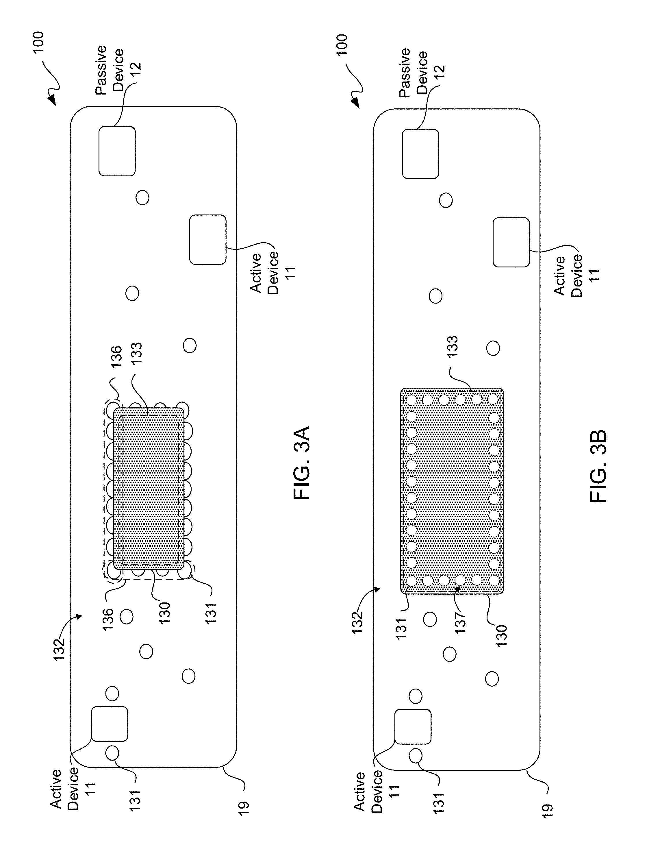
FIGS. 3A and 3B are top views of block diagrams depicting respective exemplary SiPs with EMI shielding.
FIG. 4 is a block diagram of a cross-sectional side view depicting an exemplary SiP with EMI shielding.
FIG. 5 is a block diagram of a cross-sectional side view depicting an exemplary SiP with a conductive cover and with signal wire bond wires in an EMI shielding region under the conductive cover.
FIG. 6 is a block diagram of a cross-sectional side view depicting an exemplary SiP with EMI shielding using an upper substrate.
FIG. 7 is a block diagram of a top-down view depicting an exemplary portion of a SiP prior to addition of an upper conductive surface of a Faraday cage.
FIG. 8 is a block diagram of a top-down view depicting an exemplary portion of another SiP prior to addition of an upper conductive surface of a Faraday cage.
FIG. 9A is a block diagram of a cross-sectional side view depicting an exemplary portion of a package-on-package ("PoP") device with EMI shielding.
FIG. 9B is a block diagram of a cross-sectional side view depicting an exemplary portion of another PoP device with EMI shielding.
FIG. 10 is a block diagram of a cross-sectional side view depicting an exemplary portion of another SiP
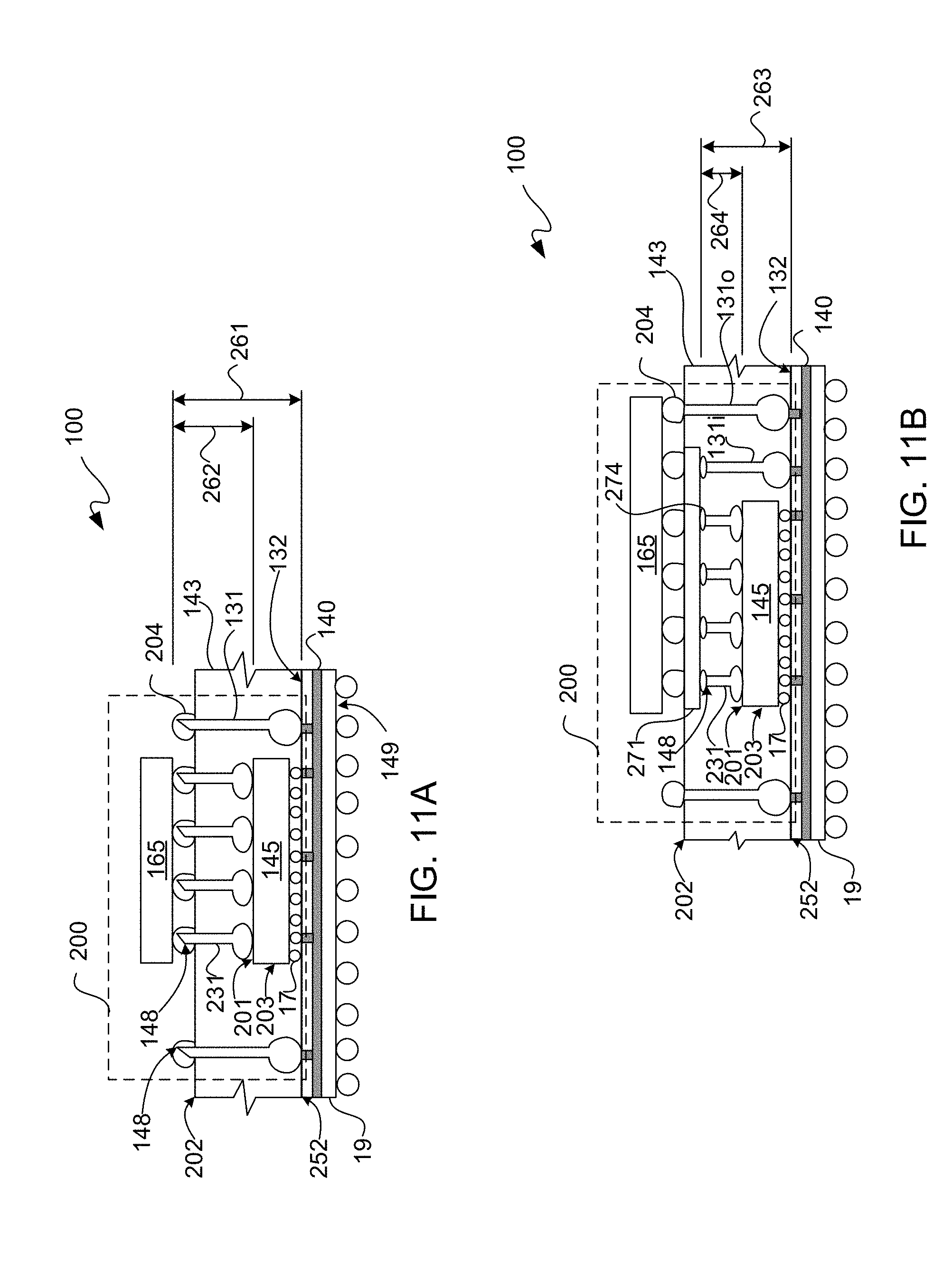
FIG. 11A is a block diagram of a cross-sectional side view depicting an exemplary portion of a SiP.
FIG. 11B is a block diagram of a cross-sectional side view depicting an exemplary portion of another SiP.
FIGS. 12A through 12D are respective block diagrams of cross-sectional side views depicting exemplary portions of respective SiPs.
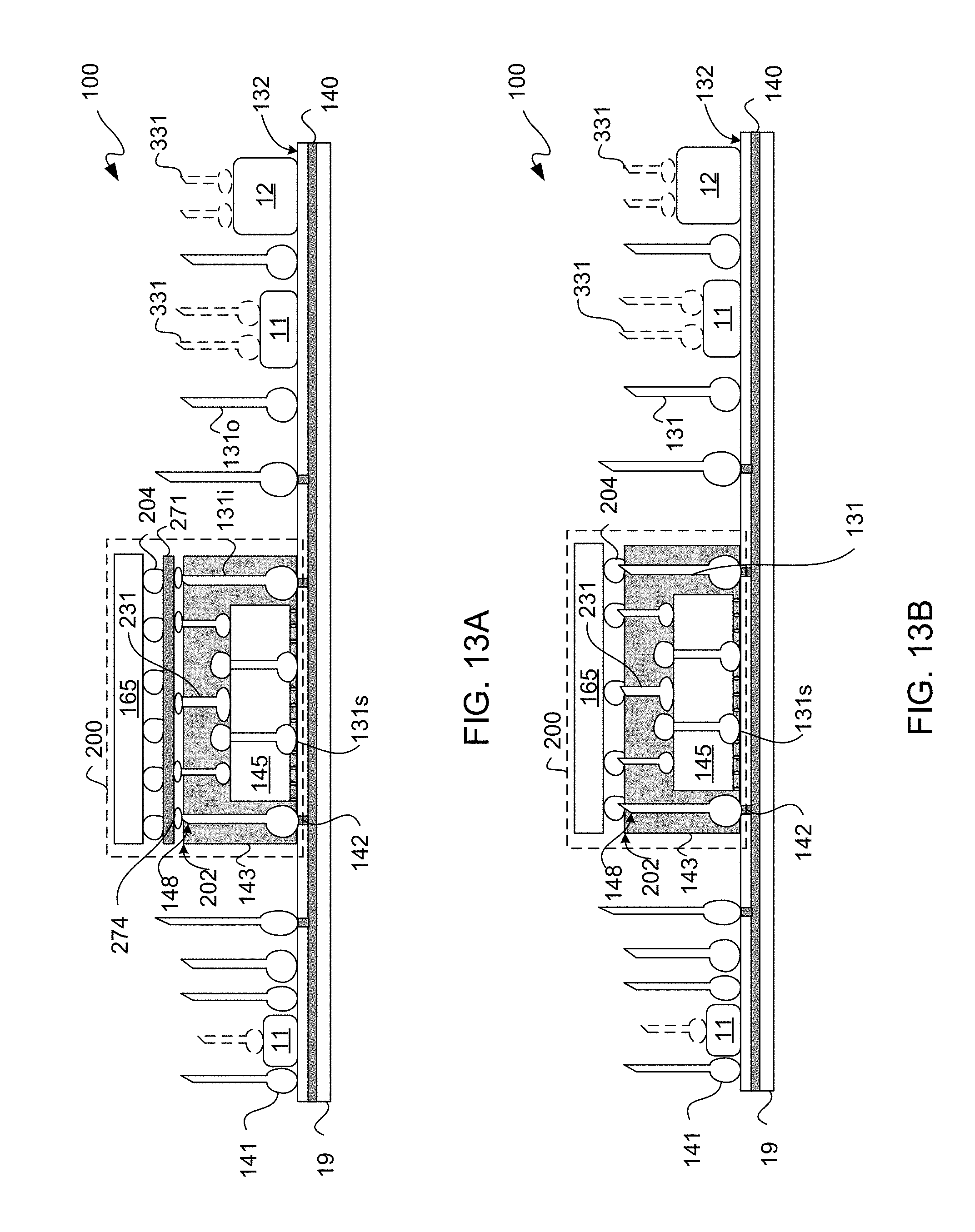
FIGS. 13A through 13D are respective block diagrams of cross-sectional side views depicting exemplary portions of respective SiPs with vertically integrated microelectronic packages.
FIGS. 14A through 14D are respective block diagrams of cross-sectional side views depicting exemplary SiPs for a vertically integrated microelectronic package.
FIGS. 15A through 15D are respective block diagrams of cross-sectional side views depicting an exemplary SiP.
FIGS. 16A and 16B are respective block diagrams of cross-sectional side views depicting exemplary SiPs 100.
FIGS. 17A through 17C are respective block diagrams of cross-sectional side views depicting exemplary inverted SiPs.
FIGS. 18A through 18D are block diagrams of side views depicting a progression formation of wire bond pads and flip-chip pads on a same substrate.
DETAILED DESCRIPTION
In the following description, numerous specific details are set forth to provide a more thorough description of the specific examples described herein. It should be apparent, however, to one skilled in the art, that one or more other examples or variations of these examples may be practiced without all the specific details given below. In other instances, well known features have not been described in detail so as not to obscure the description of the examples herein. For ease of illustration, the same number labels are used in different diagrams to refer to the same items; however, in alternative examples the items may be different.
Exemplary apparatus(es) and/or method(s) are described herein. It should be understood that the word "exemplary" is used herein to mean "serving as an example, instance, or illustration." Any example or feature described herein as "exemplary" is not necessarily to be construed as preferred or advantageous over other examples or features.
Interference in microelectronic devices may come from electric-magnetic interference ("EMI") and/or radio frequency interference ("RFI"). The following description of interference shielding may be used for either or both of these types of interference. However, for purposes of clarity by way of example and not limitation, generally only shielding from EMI is described below in additional detail.
FIG. 1A is a block diagram of a side view depicting an exemplary conventional system-in-package ("SiP"). In SiP 10, there may be coupled to a package substrate 19 one or more active microelectronic devices 11, passive microelectronic devices 12, and/or IC dies 13. In this example, IC die 13, which may be a passive or active die, may be subject to EMI. IC die 13 may be wire bonded to package substrate 19 with wire bonds 15 for carrying input/output signals among other signals, a power supply voltage and a ground reference voltage.
Package substrate 19 may be formed of thin layers called laminates or laminate substrates. Laminates may be organic or inorganic. Examples of materials for "rigid" package substrates include an epoxy-based laminate such as FR4 or FR5, a resin-based laminate such as bismaleimide-triazine ("BT"), a ceramic substrate (e.g. a low temperature co-fired ceramic ("LTCC")), a glass substrate, or other form of rigid package substrate. Moreover, a package substrate 19 herein may be a PCB or other circuit board. Other known details regarding conventional SiP 10 are not described for purposes of clarity.
FIG. 1B is a block diagram of a side view depicting another exemplary conventional SiP 10. SiP 10 of FIG. 1B is the same as SiP 10 of FIG. 1A, except rather than wire bonds 15, flip-chip ("FC") interconnects, such as microbumps, 17 are used. Even though microbump interconnects 17 are illustratively depicted, other types of die-surface mount interconnects may be used. Moreover, microbump interconnects 17 may be used in addition to wire bonds 15, though not illustratively depicted in FIG. 1B.
FIG. 2 is a corner top-down perspective view depicting an exemplary portion of a conventional EMI shielding 20. In conventional EMI shielding 20, a top electrically conductive plate 23 may be disposed over a bottom conductive plate 24, where such bottom conductive plate 24 has a larger surface area than such top conductive plate 23.
Conductive plates 23 and 24 may be respectively coupled to a package substrate 19 with rows of wire bonds 21 and 22. Thus, two sides of top plate 23 may be wire bonded with corresponding rows of wire bonds 21, and likewise two sides of bottom plate 24 may be wire bonded with corresponding rows of wire bonds 22. Non-electrically conductive spacers (not shown) may be used to insulate wire bonds 21 from bottom conductive plate 24. A microelectronic device (not shown) to be EMI shielded may be sandwiched between top and bottom conductive plates 23 and 24. This type of EMI shielding with wire bonding may be too bulky for many applications. Furthermore, there may be gaps on opposite sides with respect to wire bonds providing side EMI shielding.
Interference Shielding
FIGS. 3A and 3B are top views of block diagrams depicting respective exemplary SiPs 100 with EMI shielding. Each of SiPs 100 may include a package substrate 19 having coupled to an upper surface 132 thereof one or more active microelectronic devices 11, one or more passive microelectronic devices 12, and wire bond wires 131, where lower ends of such wire bond wires 131 may be coupled to an upper surface 132 of package substrate 19. Upper surface 132 may be a conductive surface. Wire bond wires 131 may include wire diameters equal to or less than approximately 0.0508 millimeters (2 mils).
A portion of wire bond wires 131 may be positioned to define a shielding region 133. Along those lines, rows and columns of a BVA arrangement 136 of wire bond wires 131 may be used to encircle or otherwise surround a shielding region 133. Upper ends of at least a subset of such wire bond wires 131 surrounding a shielding region 133 may be used to support conductive surface 130, and such conductive surface 130 may be over such shielding region 133 for covering thereof.
Conductive surface 130 may be a rigid or flexible surface which is electrically conductive. In an implementation, conductive surface 130 may be flexible, such as a flexible conductive coating on a surface of a flexible sheet. In another implementation, a rigid plate may provide a conductive surface. A rigid plate may be made of a conductive material. However, a conductive coating may be sprayed or painted on a rigid plate or a flexible sheet. In the example of FIG. 3B, conductive surface 130 may have holes 137 for allowing upper portions of at least some of wire bond wires 131 defining a shielding region 133 to extend through conductive surface 130, as described below in additional detail.
FIG. 4 is a block diagram of a cross-sectional side view depicting an exemplary SiP 100 with EMI shielding. SiP 100 may include a package substrate 19 having coupled to an upper surface 132 thereof one or more active microelectronic devices 11, one or more passive microelectronic devices 12, and wire bond wires 131, where upper ends of such wire bond wires 131 may be coupled to a conductive surface 130. Even though a SiP 100 is described, another type of microelectronic package having protection from EMI may be used.
Package substrate 19 has an upper surface 132 and a lower surface 149 opposite the upper surface. Package substrate 19 may have a ground plane 140 and vias 142 located between surfaces 132 and 149, where vias 142 may be interconnected to such ground plane 140 for electrical conductivity.
Wire bond wires 131 may be coupled to ground plane 140 with vias 142. Some wire bond wires 131 may be mechanically coupled to upper surface 132 with ball bonds 141 for electrical conductivity; however, in other implementations, other types of bonding may be used. Moreover, not all wire bond wires 131 need be coupled to ground plane 140. Some wire bond wires 131 may be used for carrying supply voltages or signals within SiP 100. Some wire bond wires 131 may be used for coupling to other devices within SiP 100.
An active or passive microelectronic device 145 may be coupled to upper surface 132 of package substrate 19. Microelectronic device 145 may include an active integrated circuit die and/or a passive component. A passive component may be, e.g., a capacitor, an inductor, or a resistor, or any combination thereof.
Microelectronic device 145 may be coupled to package substrate 19 with ball or bump interconnects and/or wire bond wires, as previously described. Moreover, microelectronic device 145 may be coupled to upper surface 132 with an adhesive or an underfill layer (not shown).
Microelectronic device 145 may be disposed in a dielectric protective material which may be provided as dam fill or a molding layer ("molding layer") 143. Such molding layer 143 may be an encapsulant or a molding material for at least covering an upper surface and sidewalls of microelectronic device 145. Wire bond wires 131 may be disposed around sidewalls of microelectronic device 145.
Conductive surface 130 may be located upon or coupled to a top or upper surface 146 of dielectric protective material molding layer 143. However, in another implementation a top surface of dielectric protective material molding layer 143 may be at a higher level than tips 148 of wire bond wires 131, as described below in additional detail. Conductive surface 130 may be positioned over wire bond wires 131 associated with Faraday cage 153. Upper ends or tips 148 of such wire bond wires 131 may be mechanically coupled to conductive surface 130. This coupling may be with a heated press bonding or other form of mechanical coupling.
Faraday cage 153 may be a combination of a portion of ground plane 140 interconnected to wire bond wires 131, such as with vias 142, supporting a conductive surface 130. In another implementation, there may be a gap 144 between conductive surface 130 and tips 148 of some of wire bond wires 131. Along those lines, a bottom of conductive surface 130, such as of a conductive plate for example, may be attached to or rest upon a top surface of dielectric protective material molding layer 143, and height of dielectric protective material molding layer 143 may be greater than height of wire bond wires 131.
Thus, a conductive surface 130 may be positioned over a portion of wire bond wires 131 with upper ends or tips 148 thereof spaced apart from conductive surface 130. However, a configuration with a gap 144 may provide a less effective Faraday cage 153, and so for purposes of clarity by way of example and not limitation, it shall be assumed that there is no gap.
Wire bond wires 131 coupled to ground plane 140 projecting or extending upwardly away from upper surface 132 of package substrate 19 may be arrayed. Along those lines, even though single rows and columns of a Bond Via Array.TM. or BVA.RTM. arrangement 136 of wire bond wires 131 may be present in an implementation, multiple rows and/or multiple columns of wire bond wires 131 of a BVA arrangement 136, may be present along one or more sides of a shielding region 133.
To recapitulate, some of wire bond wires 131, such as in BVA arrangement 136 defining a shielding region 133, may be positioned to provide such a shielding region 133 for microelectronic device 145 from or with respect to EMI. Another portion of wire bond wires 131 located outside of shielding region 133 may not be used for EMI shielding. Moreover, one or more other active or passive microelectronic devices 11 and/or 12 may be coupled to substrate 19 and be located outside of shielding region 133 and not part of, or positioned for such shielding region.
FIG. 5 is a block diagram of a cross-sectional side view depicting an exemplary SiP 100 with a conductive cover 150 and with signal wire bond wires 131s in an EMI shielding region under conductive cover 150. SiP 100 of FIG. 5 is the same as SiP 100 of FIG. 4, but with the following differences.
In this example, a portion of wire bond wires 131 have a height that is greater than a height of another portion of wire bond wires 131. Both sets of wire bond wires 131 may be positioned proximate to and around microelectronic device 145. However, the portion of wire bond wires 131 that are taller may be for providing a shielding region 133 for microelectronic device 145 with respect to EMI. Whereas, the other portion of wire bond wires 131 that are shorter ("wire bond wires 131s") may be signal wires coupling microelectronic device 145 to conductors of package substrate 19. Some of such shorter wire bond wires 131s may be within a Faraday cage 153. Heights of taller wire bond wires 131 may be limited by low-profile package applications.
Conductive cover 150 may be coupled to upper surface 132 of package substrate 19. Conductive cover 150 may cover components of SiP 100 coupled to upper surface 132 including microelectronic device 145, microelectronic devices 11, 12 and wire bond wires 131. Wire bond wires 131 not part of BVA arrangement 136 may interconnect conductive cover 150 and ground plane 140. This coupling may be used to reduce internal noise. However, Faraday cage 153 may be located under cover 150 for internal EMI shielding. Optionally, conductive surface 130 may be omitted in favor of using conductive cover 150 as an upper conductive surface of Faraday cage 153, with or without a gap 144 between tips 148 and an underside of conductive cover 150.
Some wire bond wires 131 within BVA arrangement 136 may be signal wires, namely wire bond wires 131s. Wire bond wires 131s may not be coupled to ground plane 140, but may be coupled to traces (not shown) of package substrate 19. Tips of wire bond wires 131s may be bonded or soldered to microelectronic device 145 prior to use of dielectric protective material molding layer 143. In another implementation, dielectric protective material molding layer 143 may be omitted with respect to microelectronic device 145.
Wire bond wires 131s may be bonded to upper surfaces of one or more of passive microelectronic devices 12 or active microelectronic devices 11. These wire bond wires 131s may be for interconnection within SiP 100.
FIG. 6 is a block diagram of a cross-sectional side view depicting an exemplary SiP 100 with EMI shielding using an upper substrate 169. SiP 100 of FIG. 6 is the same as SiP 100 of FIG. 5, but without a conductive cover 150 and with the following differences.
Upper substrate 169 may include vias 162 and a ground plane 160. Tips or upper ends 148 of wire bond wires 131 may be interconnected to vias 162 along a bottom surface of upper substrate 169 with interconnects 161, such as with micro balls or microbumps for example, for coupling to ground plane 160. Interconnects 161 may be disposed on an upper surface 168 of dielectric protective material molding layer 143. Ground plane 160 may provide an upper conductive surface 130 of Faraday cage 153.
Another microelectronic device 165, whether active or passive, may be coupled to a top surface of upper substrate 169. Microelectronic device 165 may be coupled with wire bond wires 15 to vias or traces of substrate 169; however, micro balls or microbumps may be used in another implementation. Microelectronic device 165 may be coupled outside of Faraday cage 153.
FIG. 7 is a block diagram of a top-down view depicting an exemplary portion of a SiP 100 prior to addition of an upper conductive surface 130 of a Faraday cage 153. Bond pads 170 may be positioned proximate to and around microelectronic device 145 for coupling wire bond wires 131 respectively thereto for providing shielding region 133 of Faraday cage 153. Shielding region 133 may be defined within a BVA arrangement 136.
Bond pads 170 may be spaced apart from one another around sides of dielectric protective material molding layer 143. Microelectronic device 145 in dielectric protective material molding layer 143 may be located in a central portion of shielding region 133. A pad-to-pad pitch 171 of bond pads 170 may be equal to or less than approximately 250 microns. Pitch 171 of bond pads 170 may be selected for frequencies associated with interference, such as EMI and/or RFI, to shield microelectronic device 145 from EMI and/or RFI. Moreover, microelectronic device 145 may be an interference radiator, and thus such shielding may be to protect other components of SiP 100 from interference generated by microelectronic device 145.
Even though single rows and columns of bond pads 170 are illustratively depicted, in another implementation there may be more than one or two rows and/or columns. Moreover, rows and/or columns of bond pads 170 may be interleaved with respect to one another to provide denser shielding. Effectively, wire bond wires 131 may be used to provide a low pass filter Faraday cage for reducing EMI with respect to operation of microelectronic device 145. Along those lines, placement of bond pads 170, and thus wire bond wires 131 may, though need not be, uniform. Wire bond wires 131 may be placed and/or adjusted for density tailored to shield a particular range of frequencies to or from microelectronic device 145.
FIG. 8 is a block diagram of a top-down view depicting an exemplary portion of another SiP 100 prior to addition of an upper conductive surface 130 of a Faraday cage 153. In this example, two rows and two columns of a BVA arrangement 136 of wire bond wires 131 are used to define a shielding region 133. In this example, spacing between rows and columns is interleaved to provide a denser pattern of wire bond wires 131.
In this example, some of wire bond wires 131 of BVA arrangement 136 are for carrying signals, namely wire bond wires 131s. Along those lines, interconnects 180 may be formed for extending from microelectronic device 145 outside of dielectric protective material molding layer 143 for interconnection with wire bond wires 131s, which may include one or more signal wires.
FIG. 9A is a block diagram of a cross-sectional side view depicting an exemplary portion of a package-on-package ("PoP") device 190 with EMI shielding. PoP device 190 may include an upper SiP 100U stacked on top of a lower SiP 100L. PoP device 190 may include one or more other microelectronic devices outside of a shielding region as well as other details, such as previously described with reference to FIGS. 3A through 8 for example. Accordingly, previously described details for SiPs 100 are not described hereinbelow for purposes of clarity and not limitation.
A lower package substrate 19L of a lower SiP 100L may include a lower ground plane 140L having lower wire bond wires 131L extending upwardly from an upper surface of lower package substrate 19L. Such lower wire bond wires 131L and ground plane 140L may be interconnected to one another, such as with vias and ball bonds as previously described, for forming a lower portion of a Faraday cage 153. Tips 148 of lower wire bond wires 131L may be bonded or coupled with interconnects 191 to pads and vias therefor along an underneath side of upper package substrate 19U.
Optionally, upper package substrate 19U may include an upper ground plane 140U for forming a Faraday cage 153 as a stack of two Faraday cages, namely an upper Faraday cage 192U and a lower Faraday cage 192L. Each of Faraday cages 192U and 192L may include respective packaged microelectronic devices 145U and 145L respectively coupled to upper surfaces of package substrates 19U and 19L.
Upper ground plane 140U of upper substrate 19U may be located over a lower microelectronic device 145L, so tips or upper ends 148 of lower wire bond wires 131L may be interconnected to pads or contacts with interconnects 191 along an underside surface of upper package substrate 19U for electrical coupling to upper ground plane 140U. Upper wire bond wires 131U and optional ground plane 140U may be interconnected to one another, such as with vias and ball bonds as previously described, for forming an upper portion of a Faraday cage 153. Tips 148 of upper wire bond wires 131U may be bonded or coupled to conductive surface 130 for completing such upper Faraday cage 192U.
In another implementation, vias of upper substrate package 19U may interconnect lower wire bond wires 131L with upper wire bond wires 131U without being connected to an upper ground plane 140U to form a "two-story" or bi-level Faraday cage 153 for two microelectronic devices 145U, 145L. Even though only two levels are illustratively depicted, more than two levels may be used in other implementations.
FIG. 9B is a block diagram of a cross-sectional side view depicting an exemplary portion of another PoP device 190 with EMI shielding. PoP device 190 may include one or more other microelectronic devices outside of a shielding region as well as other details, such as previously described with reference to FIGS. 3A through 9A for example. Accordingly, previously described details for SiPs 100 are not described hereinbelow for purposes of clarity and not limitation.
PoP device 190 of FIG. 9B may be the same as PoP device 190 of FIG. 9A, except with the following differences. PoP device 190 of FIG. 9B may include signal wire bond wires 131s. Signal wire bond wires 131s may be located within Faraday cage 153, including within Faraday cage 192U.
Signal wire bond wires 131s in this configuration may extend upwardly from an upper surface of a lower microelectronic device 145L. Tips or upper ends 148 of wire bond wires 131s extending from an upper surface of lower microelectronic device 145L may be interconnected to an underneath side of upper package substrate 19U, such as with interconnects 191. Vias and/or traces (not shown) may electrically couple upper and low microelectronic devices 145 with signal wire bond wires 131s. Moreover, lower substrate package 19L may include vias and/or traces (not shown) for interconnection with lower microelectronic device 145.
FIG. 10 is a block diagram of a cross-sectional side view depicting an exemplary portion of another SiP 100. SiP 100 may include one or more other microelectronic devices outside of a shielding region as well as other details, such as previously described with reference to FIGS. 3A through 9B for example. Accordingly, previously described details for SiPs 100 are not described hereinbelow for purposes of clarity and not limitation.
In this example, wire bond wires 131 and a microelectronic device 145, such as an IC die, are protected by a dielectric protective material molding layer 143. Microelectronic device 145 may be interconnected with microbump interconnects 17 to an upper surface of package substrate 19 prior to depositing or injecting dielectric protective material molding layer 143. Likewise, wire bond wires 131 may be ball bonded to an upper surface of package substrate 19 prior to depositing or injecting dielectric protective material molding layer 143.
Optionally, signal wire bond wires 131s may be ball bonded to an upper surface 201 of microelectronic device 145 prior to depositing or injecting dielectric protective material molding layer 143. Signal wire bond wires 131s thus may be within a shielding region 133 of a Faraday cage 153.
Tips or upper ends 148 of wire bond wires 131, as well as optional signal wire bond wires 131s, may extend above an upper surface 202 of dielectric protective material molding layer 143. Solder balls or other interconnect eutectic masses 204 may be deposited onto tips 148 for subsequent interconnection, such as described elsewhere herein.
Vertical Integration without Interference Shielding
FIG. 11A is a block diagram of a cross-sectional side view depicting an exemplary portion of a SiP 100. FIG. 11B is a block diagram of a cross-sectional side view depicting an exemplary portion of another SiP 100. With simultaneous reference to FIGS. 11A and 11B, SiPs 100 respectively illustratively depicted in those figures are further described. Each of SiPs 100 may include one or more other microelectronic devices as well as other details, such as previously described. Accordingly, previously described details for SiP 100 are not described hereinbelow for purposes of clarity and not limitation.
Each of SiPs 100 includes a vertically integrated microelectronic package 200. Each of microelectronic packages 200 includes a substrate 19 having an upper surface 132 and a lower surface 149 opposite the upper surface. Package substrate 19 may have located between surfaces 132 and 149 a ground plane 140 and vias 142 interconnected to such ground plane for electrical conductivity.
A microelectronic device 145 may be coupled to upper surface 132 of substrate 19, where microelectronic device is a passive microelectronic device. Along those lines, in a SiP 100 there may be one or more of either or both passive or active microelectronic devices coupled to upper surface 132. This means there are upper surfaces of such microelectronic devices that in the past may have gone unused for vertical integration, such as by having bonding wire bond wires attached to such upper surfaces of such microelectronic devices as described herein.
Along those lines, wire bond wires 131 may be coupled to and extend away from the upper surface 132 of substrate 19, and wire bond wires 231 may be coupled to and extend away from an upper surface 201 of microelectronic device 145. Wire bond wires 131 and 231 may be mechanically coupled to upper surfaces 132 and 201, respectively, with ball bonds 141 for electrical conductivity. However, in other implementations, other types of bonding may be used. Wire bond wires 231 are shorter in length than wire bond wires 131.
With reference to FIG. 11A, wire bond wires 131 may have an overall finished length 261, and wire bond wires 231 may have an overall finished length 262. However, finished heights of wire bond wires 131 and 231 may be approximately the same. Tips or upper ends 148 of wire bond wires 131 and 231 may extend above an upper surface 202 of molding layer 143.
Upper ends 148 may be coterminous for being generally coplanar. Solder balls or other interconnect eutectic masses 204 may be deposited on upper surface 202 respectively over upper ends 148 for forming interconnects with pads (not shown) on a front face underside of an active or a passive microelectronic device 165.
A passive microelectronic device 145 may be coupled to upper surface 132 of package substrate 19. Microelectronic device 145 may include conductive traces and may include only passive components. A passive component may include one or more of a capacitor, an inductor, or a resistor, or any combination thereof.
Microelectronic device 145 may be coupled to package substrate 19 with ball or bump interconnects and/or wire bond wires, as previously described. Moreover, microelectronic device 145 may be coupled to upper surface 132 with an adhesive or an underfill layer (not shown).
In this implementation, microelectronic device 145, as well as a microelectronic device 165, may have orientations facing downwardly, namely face-down orientations, toward upper surface 132 of substrate 19. However, in another implementation, microelectronic device 165 may have a front side face facing upwardly away from an upper surface 132 of substrate 19.
A microelectronic device 165 may be coupled above uppermost surface 202 of molding layer 143. In an implementation, a microelectronic device 165 may be coupled to upper ends 148 of wire bond wires 131 and 231 with eutectic masses 204 or other mechanical interconnects. Microelectronic device 165 may be located above microelectronic device 145 and at least partially overlap such microelectronic device 145.
Molding layer 143 may have an uppermost surface 202 and a lowermost surface 252 opposite the uppermost surface. Molding layer 143 may be disposed for surrounding portions of lengths 261 and 262 for both wire bond wires 131 and 231. Upper ends 148 may not be covered with molding layer 143, such as by use of a mold assist film for an injection molding for example. In another implementation, molding layer 143 may temporarily completely cover lengths 261 and 262 followed by an etch back to reveal upper ends 148.
In an implementation of a vertically integrated microelectronic package 200, microelectronic device 145 may be disposed in molding layer 143. Along those lines, in an implementation, microelectronic device 145 may be completely located between uppermost surface 202 and lowermost surface 252 of molding layer 143. Wire bond wires 131 may be disposed around sidewalls 203 of microelectronic device 145 though not for interference shielding in this example implementation.
Wire bond wires 131 may be coupled to ground plane 140 for projecting or extending upwardly away from upper surface 132 of package substrate 19 and may be arrayed. Along those lines, even though single rows and columns of a BVA.RTM. arrangement of wire bond wires 131 and/or 231 may be present in an implementation, multiple rows and/or multiple columns of such wire bond wires may be in a BVA.RTM. arrangement.
In an implementation of vertically integrated microelectronic package 200, microelectronic device 165, which is a passive microelectronic device, may be used. However, in another implementation of vertically integrated microelectronic package 200, microelectronic device 165, which is an active microelectronic device, may be used.
With reference to FIG. 11B, inner wire bond wires 131i may have an overall finished length 263, and wire bond wires 231 may have an overall finished length 264. Outer wire bond wires 131o may have an overall finished height 261, as previously described with reference to FIG. 11A. Finished heights of wire bond wires 131i and 231 may be approximately the same after forming. Upper ends 148 of wire bond wires 131i and 231 may generally even with one another.
Upper ends 148 of wire bond wires 131i and 231 may be coterminous for being generally coplanar. Solder balls or other interconnect eutectic masses 274 may couple a lower surface of an active or passive microelectronic device 271 respectively to upper ends 148 of wire bond wires 131i and 231 for forming interconnects with pads (not shown) on a front face underside of an active or passive microelectronic device 271. A molding material may be injected to form molding material layer 143 with microelectronic device 271 in place, and thus a lower surface of microelectronic device 271 may be in contact with molding material of molding layer 143. For molding, a mold assist film may be used to allow tips 148 of outer wire bond wires 131o to extend above upper surface 202 of molding layer 143, as well as pads or other interconnects (not shown) of microelectronic device 271. In another implementation, molding layer 143 may temporarily completely cover lengths 261 followed by an etch back to reveal upper ends 148 thereof.
Microelectronic device 271 may be coupled to and located above microelectronic device 145 and may at least partially overlap microelectronic device 145. Along those lines, microelectronic device 271 may laterally extend outside a perimeter of microelectronic device 145 for interconnection of inner wire bond wires 131i between upper surface 132 of substrate 19 and a lower surface of microelectronic device 271 facing such upper surface 132. Wire bond wires 131i, as well as wire bond wires 131o, may be disposed around sidewalls 203 of microelectronic device 145 though not for interference shielding in this example implementation.
Again, a passive microelectronic device 145 may be coupled to upper surface 132 of package substrate 19. Microelectronic device 145 may include conductive traces and may include only active components, only passive components or a combination thereof. A passive component may include a capacitor, an inductor, or a resistor, or any combination thereof. Microelectronic device 145 may be coupled to package substrate 19 with ball or bump interconnects and/or wire bond wires, as previously described. Moreover, microelectronic device 145 may be coupled to upper surface 132 with an adhesive or an underfill layer (not shown).
Molding layer 143 may have an uppermost surface 202 and a lowermost surface 252 opposite the uppermost surface. Molding layer 143 may be disposed for surrounding portions of lengths 261 of wire bond wires 131o and for surrounding lengths 263 and 264 for both wire bond wires 131i and 231.
In an implementation of vertically integrated microelectronic package 200, microelectronic device 145 may be disposed in molding layer 143 and completely located between uppermost surface 202 and lowermost surface 252 of molding layer 143. Microelectronic device 271 may be disposed in molding layer 143 and at least partially located between uppermost surface 202 and lowermost surface 252 of molding layer 143. Microelectronic device 165 may be coupled above uppermost surface 202 of molding layer 143.
For a passive microelectronic device 271, microelectronic device 271 may include conductive traces and may include only passive components. Microelectronic device 271 may include an RDL. A passive component may be a capacitor, an inductor, or a resistor, or any combination thereof. In this implementation, microelectronic devices 145 and 271, as well as microelectronic device 165, have orientations facing downwardly, namely face-down orientations, toward upper surface 132 of substrate 19. However, in another implementation, microelectronic device 165 and/or microelectronic device 271 may have a front side face facing upwardly away from an upper surface 132 of substrate 19.
In an implementation of vertically integrated microelectronic package 200, microelectronic device 165, which is a passive microelectronic device, may be used. However, in another implementation of vertically integrated microelectronic package 200, microelectronic device 165, which is an active microelectronic device, may be used. A microelectronic device 165 may be coupled above uppermost surface 202 of molding layer 143 for interconnection with microelectronic device 271. In an implementation, a microelectronic device 165 may be coupled to an upper surface of microelectronic device 271 with eutectic masses 204 or other mechanical interconnects for electrical conductivity.
Microelectronic device 165 may be located above microelectronic device 271 and at least partially overlap such microelectronic device 271. Along those lines, a microelectronic device 165 may be coupled above uppermost surface 202 of molding layer 143 for interconnection with upper ends 148 of outer wire bond wires 131o, as well as interconnection with an upper surface of microelectronic device 271.
Wire bond wires 131i and 131o may be coupled to ground plane 140 for projecting or extending upwardly away from upper surface 132 of package substrate 19 and may be arrayed. Along those lines, even though single rows and columns of a BVA.RTM. arrangement of wire bond wires 131i, 131o, and/or 231 may be present in an implementation, multiple rows and/or multiple columns of such wire bond wires may be in a BVA.RTM. arrangement.
FIG. 12A is a block diagram of a cross-sectional side view depicting an exemplary portion of another SiP 100. SiP 100 of FIG. 12A may be the same as in FIG. 11A, except for the following details. In this implementation of a vertically integrated microelectronic package 200, microelectronic device 165 may be cantilevered for laterally extending over and above a wire bond wire 131. Along those lines, upper ends 148 of wire bond wires 131 may be interconnected with eutectic masses 204 to a lower surface of a microelectronic device 165.
FIG. 12B is a block diagram of a cross-sectional side view depicting an exemplary portion of another SiP 100. SiP 100 of FIG. 12B may be the same as in FIG. 11B, except for the following details. In this implementation of a vertically integrated microelectronic package 200, microelectronic device 165 is not cantilevered for laterally extending over and above a wire bond wire 131i. Along those lines, microelectronic device 165 and microelectronic device 271 may have approximately equal surface areas for lower and upper surfaces respectively thereof.
FIG. 12C is a block diagram of a cross-sectional side view depicting an exemplary portion of another SiP 100 with or without integrated wire bond wire EMI shielding. SiP 100 of FIG. 12C may be the same as in FIG. 12A, except for the following details. In this implementation of a vertically integrated microelectronic package 200, microelectronic device 165 is cantilevered for laterally extending over and above wire bond wires 131 on both a right and a left side of microelectronic device 145 in the figure. Along those lines, upper ends 148 of wire bond wires 131 may be interconnected with eutectic masses 204 to a lower surface of a microelectronic device 165. Accordingly, it should be appreciated that wire bond wires 131 disposed around a microelectronic device and interconnected to a microelectronic device 165 may be used for fan-out.
FIG. 12D is a block diagram of a cross-sectional side view depicting an exemplary portion of another SiP 100 with or without integrated wire bond wire EMI shielding. SiP 100 of FIG. 12D may be the same as in FIG. 12B, except for the following details. In this implementation of a vertically integrated microelectronic package 200, microelectronic device 165 is not cantilevered for laterally extending over and above a wire bond wire 131o. Along those lines, microelectronic device 165 and microelectronic device 271 may have approximately equal surface areas for lower and upper surfaces respectively thereof. Along those lines, upper ends 148 of wire bond wires 131i may be interconnected with eutectic masses 274 to a lower surface of a microelectronic device 271. Accordingly, it should be appreciated that wire bond wires 131i disposed around a microelectronic device 145 and interconnected to a microelectronic device 271 may be used for fan-out.
FIG. 13A is a block diagram of a cross-sectional side view depicting an exemplary SiP 100 with a vertically integrated microelectronic package 200. In this implementation, a vertically integrated microelectronic package 200 may be a stand-alone package coupled to substrate 19 as in FIG. 12D of a SiP 100. As components of SiP 100 have been previously described, such as with reference to FIG. 4 for example, such description is not repeated.
In this implementation, eutectic masses 274, such as solder balls, are formed on an upper surface 202 of molding layer 143, on a redistribution layer, or on tips of the wire bond wire bond wires 131i and 231. Eutectic masses 274 interconnect upper ends 148 of wire bond wires 131i and 231 to a lower surface of microelectronic device 271. In another implementation, eutectic masses 274 may be encapsulated in molding layer 143. In this example, a lower surface of microelectronic device 271 is not in contact with an upper surface 202 of molding layer 143.
Moreover, in this example implementation, signal wire bond wires 131s may be encapsulated in molding material of molding layer 143, excluding contact ends thereof. Signal wire bond wires 131s may be shorter than inner wire bond wires 131i and may be as previously described for interconnection with a microelectronic device 145. Along those lines, microelectronic device 271 may be coupled to upper ends 148 of a taller portion of wire bond wires 131 coupled to upper surface 132, such as wire bond wires 131i. Microelectronic device 271 may further be coupled to upper ends 148 of wire bond wires 231. Another portion of wire bond wires 131 coupled to upper surface 132, such as signal wire bond wires 131s, may have upper ends 148 thereof coupled to an upper surface of microelectronic device 145, such as previously described.
Optionally, wire bond wires 331 may be coupled to one or more upper surfaces of active microelectronic devices 11 and/or passive microelectronic devices 12, which microelectronic devices 11 and/or 12 are directly coupled to an upper surface 132 of substrate 19.
Other details regarding SiP 100 of FIG. 13A have been previously described, and thus are not repeated for purposes of clarity and not limitation.
FIG. 13B is a block diagram of a cross-sectional side view depicting another exemplary SiP 100 with a vertically integrated microelectronic package 200. In this implementation, a vertically integrated microelectronic package 200 may be a stand-alone package coupled to substrate 19 as in FIG. 13A of a SiP 100. As components of SiP 100 have been previously described, such as with reference to FIG. 4 for example, such description is not repeated.
SiP 100 of FIG. 13B is similar to SiP 100 of FIG. 13A, except for the following differences. In SiP 100 of FIG. 13B, vertically integrated microelectronic package 200 omits microelectronic device 271. Thus, a microelectronic device 165 may be directly coupled to an upper surface 202 of molding layer 143 with eutectic masses 204, such as previously described.
FIG. 13C is a block diagram of a cross-sectional side view depicting yet another exemplary SiP 100 with a vertically integrated microelectronic package 200. In this implementation, a vertically integrated microelectronic package 200 may be a stand-alone package coupled to substrate 19 as in FIG. 13A of a SiP 100. As components of SiP 100 have been previously described, such as with reference to FIG. 4 for example, such description is not repeated.
SiP 100 of FIG. 13C is similar to SiP 100 of FIG. 13A, except for the following differences. In SiP 100 of FIG. 13C, vertically integrated microelectronic package 200 has some wire bond wires 131i encapsulated in molding material of molding layer 143 as previously described and has some wire bond wires 131i not encapsulated in molding material of molding layer 143.
FIG. 13D is a block diagram of a cross-sectional side view depicting still yet another exemplary SiP 100 with a vertically integrated microelectronic package 200. In this implementation, a vertically integrated microelectronic package 200 may be a stand-alone package coupled to substrate 19 as in FIG. 13B of a SiP 100. As components of SiP 100 have been previously described, such as with reference to FIG. 4 for example, such description is not repeated.
SiP 100 of FIG. 13D is similar to SiP 100 of FIG. 13B, except for the following differences. In SiP 100 of FIG. 13D, vertically integrated microelectronic package 200 does not have wire bond wires 131 encapsulated in molding material of molding layer 143.
FIG. 14A is a block diagram of a cross-sectional side view depicting further another exemplary SiP 100 with a vertically integrated microelectronic package 200. As SiP 100 of FIG. 14A is similar to SiPs 100 previously described herein, generally only the differences are described below in additional detail for purposes of clarity.
In this example implementation, a circuit platform 400 may be a package substrate such as package substrate 19, a die substrate or interposer, a lead frame, or a routing layer, such as an RDL for example. In this example, a passive microelectronic device 271 is generally represented as a circuit platform 401, which may be a routing layer, a die substrate or interposer, or a package substrate. Vertical wire bond wires 131i may interconnect an upper surface 405 of circuit platform 400 to a lower surface 403 of circuit platform 401. In this example, microelectronic device 145 is a wire bond-only device, which has a lower surface 406 thereof coupled to an upper surface 405 of circuit platform 401 with an epoxy or other adhesive layer 402 between such facing surfaces.
Microelectronic device 145 may be in a face-up orientation. Wire bond wires 131s may interconnect an upper surface 405 of circuit platform 401 to an upper surface 407 of microelectronic device 145. Shorter vertical wire bond wires 231 may interconnect an upper surface 407 of microelectronic device 145 with a lower surface 403 of circuit platform 401.
Dielectric protective material molding layer 143 may be a molding layer or a dam-fill layer and, while shown only covering a portion of the SIP, may alternatively cover any or all of the components in the SIP 100. Microelectronic device 145 may be coupled with adhesive layer 402 to circuit platform 400, followed by wire bonding wire bond wires 131s and 231. Wire bond wires 231 and 131i may be coupled to a lower surface 403 of circuit platform 401, prior to adding a molding or dam-filling layer of dielectric protective material molding layer 143. Dielectric protective material may provide a more rigid structure than just having wire bond wires 131i and 231 support circuit platform 401, as a lower surface 403 and at least portions of a sidewall surface(s) 404 may be covered with such dielectric protective material molding layer 143.
FIG. 14B is a block diagram of a cross-sectional side view depicting further yet another exemplary SiP 100 with a vertically integrated microelectronic package 200. As SiP 100 of FIG. 14B is similar to SiP 100 of FIG. 14A, generally only the differences are described below in additional detail.
In addition to wire bond wires 231 on an upper surface 407 of microelectronic device 145, another microelectronic device 410 may have a lower surface thereof coupled to an upper surface of microelectronic device 145 with another epoxy or other adhesive layer 402 between such facing surfaces. Another set of interconnects provided with vertical wire bond wires 432 may be coupled between an upper surface of microelectronic device 410 and a lower surface 403 of circuit platform 401 for electrical communication between microelectronic device 410 and circuit platform 401. Microelectronic devices 145 and 410 may in combination form a die stack with both of such devices in a face-up orientation for wire bonding to upper surfaces thereof.
Furthermore, in addition to having a starting placement of wire bond wires 231 and microelectronic device 410 on upper surface 407 of microelectronic device 145, another set of wire bond wires 431 may be coupled to upper surface 407 for interconnection with an upper surface 408 of microelectronic device 410. Wire bond wires 431 may arc over for coupling to upper surface 408. These wire bond wires 431 may thus interconnect upper faces of microelectronic devices 145 and 410 to one another. Microelectronic devices 145 and 410 may be active devices, passive devices, or a combination of active and passive devices.
With simultaneous reference to FIGS. 14A and 14B, coupled to circuit platform 401 may be either or both a surface mount technology ("SMT") component, which may be an active or a passive SMT microelectronic device 165, and a wire bond mount component, such as an active or a passive wire bond microelectronic device 411. An active or a passive SMT microelectronic device 165 may be mounted face down to an upper surface 441 of circuit platform 401, and an active or a passive wire bond microelectronic device 411 may be mounted face-up to upper surface 441 of circuit platform 401.
FIG. 14C is a block diagram of a cross-sectional side view depicting still further yet another exemplary SiP 100 with a vertically integrated microelectronic package 200. As SiP 100 of FIG. 14B is similar to SiP 100 of FIGS. 14A and 14B, generally only the differences are described below in additional detail.
In this example implementation, a lower surface of an interposer or other circuit platform 414 is interconnected to contacts on an upper surface of a face-up microelectronic device 145 with microbumps or other small form factor interconnects 413. An upper surface of interposer 414 is interconnected to contacts on a lower surface of a face-down microelectronic device 416 with microbumps or other small form factor interconnects 415. Distal ends of wire bond wires 131s may be coupled to an upper surface of interposer 414 for interconnection to an upper surface 405 of circuit platform 400. Proximal or lower ends of wire bond wires 231 may be coupled to an upper surface of interposer 414, with distal or upper ends of such wire bond wires coupled to lower surface 403 of circuit platform 401. By using an interposer 414 and flip-chip or like microelectronic device 416, more area for wire bond wires 231 and/or 131s may be provided, along with more interconnections between microelectronic devices 145 and 416.
FIG. 14D is the block diagram of FIG. 14C, though with a molding layer of a protective dielectric material 143 covering circuit platform 400. This molding layer of protective dielectric material 143 provides interconnect surface 418 above an upper surface 405 of circuit platform 400. Wire bond wires 131 and 331 may have tips or upper ends thereof extend above surface 418 for interconnection of one or more passive or active circuits.
These are some of a variety of implementations of a vertically integrated microelectronic package 200 for a SiP 100. These or other implementations may be provided in accordance with the description herein. However, above implementations with intermingling of SMT and wire bond devices have been described. As described in additional detail below, surfaces or at least portions thereof may be reserved for either SMT-only or wire bond-only devices.
Vertical Integration with Separation of Mounting Surface Types
Routings, such as traces and vias, over large distances with respect to coupling microelectronic devices, including without limitation one or more VLSI die, in a multi-die package coupled to a circuit board may result in significant current-resistance drops ("IR drops") or voltage drops. Along those lines, conventionally, VLSI dies have been designed with bond pads or other wire bond contacts at or around a periphery of such dies or packages for interconnection of wire bonds. Moreover, as VLSI dies and multi-die packages become larger, distances to active areas or distances to components, respectively, becomes longer, and these longer distances may result in correspondingly larger IR drops. With respect to VLSI dies and multi-die packages, differences in lengths of, as well as differences in parasitic effects on, routings may cause differences or variations in signals transported thereon. With respect to integrated circuit dies, these on-chip differences may be referred to as on-chip variation ("OCV"). Such differences may affect voltage level, timing (i.e., signal propagation delay), and/or signal interaction, as well as other parameters. In some instances, a VLSI die or a multi-die package may be slowed and/or draw additional power to account for such OCVs or IR drops.
With the above context borne in mind, routing distances, such as for VLSI dies and/or SiPs are further described. To reduce the effect of IR drops, capacitance may be added, as is known, to adjust a resistance-capacitance ("RC") timing delay. However, capacitors may be large and not readily integrated into a VLSI process, and thus external capacitors may be coupled to a VLSI die. SiP applications may include without limitation one or more VLSI die wire bonded to a platform along with one or more SMT components coupled to a same platform. SiPs may be used in RF as well as other applications, which may include surface mount components, such as oscillators, capacitors, couplers, and/or diplexers among other components.
In a SiP, wire bond and surface mount components may be mounted together on a same mounting surface. Along those lines, surface mount components may be coupled to a package substrate, such as an interposer or a lead frame, or a routing layer, such as an RDL, with gaps between such surface mount components for subsequent mounting of wire bond components to such package substrate or routing layer. These gaps may be sufficiently wide to avoid having solder flux and/or solder, or other material associated with a eutectic coupling, contaminate wire bonding pads or wire bonding contacts. This spacing effectively increases IR drops by increasing distances between components.
As described below in additional detail, a SiP or other multi-microelectronic device package may have a circuit platform which has a wire bond-only surface or has a portion for two or more wire bond-only components without any surface mount technology ("SMT") components between such two or more wire bond-only components. A molding or dam-fill layer may be added over and on such circuit platform of wire bonded components, such as one or more VLSI die for example, to provide a surface mount-only area, namely a surface mount technology-only ("SMT-only") surface area ("SMT-only area"), which at least partially corresponds to such wire bond-only surface area or surface area portion ("wire bond-only area").
FIG. 15A is a block diagram of a cross-sectional side view depicting an exemplary SiP 100. SiP 100 is a vertically integrated microelectronic package including a circuit platform 400 having an upper surface 405 and a lower surface 505 opposite such upper surface thereof. Balls or other interconnects 501 may be coupled to lower surface 505. One or more integrated circuit dies or other microelectronic devices 502 and/or 503 may be coupled to upper surface 405. In this example, integrated circuit dies 502 are coupled to upper surface 405 with microbumps 413. In this example, integrated circuit dies 503 are coupled to upper surface 405 with an adhesive layer 402. Moreover, in this example, integrated circuit dies 502 and 503 are active components, but in another implementation one or more of such integrated circuit dies 502 and/or 503 may be passive components.
A portion 508 of the area of upper surface 405 may be a wire bond-only area for coupling of one or more integrated circuit dies 503, and another portion 509 of the area of upper surface 405 may be an SMT-only area for coupling of one or more integrated circuit dies 502. To avoid flux or other contamination of an SMT-only area from contaminants associated with wire bonding, areas 508 and 509 may be spaced apart from one another by a gap area 507.
SMT integrated circuit dies 502 may be coupled in a face-down orientation in SMT-only area 509, and wire bonded integrated circuit dies 503 may be coupled in a face-up orientation in wire bond-only area 508. Wire bond wires 131 may be coupled to and extend away from wire bond-only area 508 of upper surface 405 for interconnection to a passive microelectronic device 512. Wire bond wires 131 may be outside of a perimeter of a corresponding integrated circuit die 503.
Wire bond wires 231 may be coupled to and extend away from an upper surface 407 of microelectronic device 503 for interconnection to a passive microelectronic device 512, where wire bond wires 231 may be shorter than wire bond wires 131. Wire bond wires 231 may be inside of a perimeter of a corresponding integrated circuit die 503. Passive microelectronic device 512 may be located above and at least partially overlap upper surface 407.
Microelectronic device 512 may be coupled to upper ends of wire bond wires 131 and 231. Wire bond wires 531 may be coupled to upper surface 405 in wire bond-only area 508 and to upper surface 407. Wire bond wires 509 may be coupled to upper surfaces 407 of neighboring integrated circuit dies 503 in wire bond-only area 508. Along those lines, one or more passive microelectronic devices 512 may be above and within wire bond-only area 508. Neighboring integrated circuit dies 503 within wire bond-only area 508 may have wire bond wires, such as wire bond wires 531 and 131, coupled to upper surface 405 between sidewalls/perimeters of such integrated circuit dies 503 without any SMT devices in such space between such integrated circuit dies 503.
A molding layer 143 may be disposed over circuit platform 400 and one or more microelectronic devices 502 and 503. Molding layer 143 may be disposed for surrounding at least portions of lengths of wire bond wires 131 and 231 and for covering wire bond wires 509 and 531. Along those lines, upper ends of wire bond wires 131 and 231 may extend above an upper surface 202 of molding layer 143. Molding layer 143 may have a lower surface 252 in contact with upper surface 405 and may have an upper surface 202 opposite such lower surface 252. Upper surface 202 may be an SMT-only surface or have a portion thereof which is SMT-only, such as SMT-only portion or area 510. SMT-only area 510 may be opposite to and may correspond with wire bond-only area 508.
One or more passive microelectronic devices 512 may be disposed on upper surface 202 in a face-down orientation for coupling contacts thereof to upper ends of wire bond wires 131 and 231. This SMT coupling may be performed by a Thermosonic bonding or reflow soldering operation.
To recapitulate, one or more integrated circuit dies 502 and/or 503 may be disposed in molding layer 143, thus completely located between upper surfaces 202 and 405. However, one or more microelectronic devices 512 may be coupled above upper surface 202 in an SMT-only area 510, which may correspond to a wire bond-only area 508.
By positioning one or more microelectronic devices 512 in close proximity to an integrated circuit die 503 by use of wire bond wires 131 and 231, as compared routings, such as traces and vias, through a circuit board resulting in over longer distances, significant reductions in IR drops may be obtained. Moreover, because differences in lengths of, as well as differences in parasitic effects on, routings may cause differences or variations in signals transported thereon, by having shorter distances to travel these differences may be reduced by use of wire bond wires 131 and 231.
To reduce the effect of IR drops, capacitance may be added, as is known, to adjust an RC timing delay. However, capacitors may be large and not readily integrated into a VLSI process, and thus external capacitors may be coupled to a VLSI die. Thus, by having an ability to have capacitors significantly larger than those in a VLSI die, RC timing delay may be more readily addressed. Moreover, such additional capacitance may be added to a central region of a VLSI die, where RC delay from signals from bond pads around a periphery of such a VLSI die may take a significant amount of time to reach a central interior region of such a VLSI die. SiPs 100 may be used in RF as well as other applications, which may include surface mount components, such as oscillators, capacitors, couplers, and/or diplexers among other passive SMT components 512 coupled to surface 202.
In a SiP 100, wire bond and surface mount components may be mounted together on separate mounting surfaces. Along those lines, wire bond components may be coupled to a package substrate, such as an interposer or a lead frame, or a routing layer, such as an RDL, with narrower gaps in wire bond-only area 508 between such wire bond components than a mix of SMT and wire bond components mounted in an area outside of such wire bond-only area 508 to such package substrate or routing layer. Gaps between components in a wire bond-only area 508 may be sufficiently wide to avoid having solder flux and/or solder, or other material associated with a eutectic coupling, contaminate neighboring wire bonding pads but such gaps may be substantially narrower than gaps for having SMT components in such mix. This wire bond-only spacing effectively decreases IR drops by decreasing distances between components, namely by effectively relocating for example a passive microelectronic device 512 to upper surface 202 rather than mounting such component on lower surface 252.
As described above in additional detail, a SiP 100 or other multi-microelectronic device package 100 may have a circuit platform 400 which has a wire bond-only surface 508 or has a surface portion 508 for wire bond-only components without any SMT components between such wire bond-only components. A molding or dam-fill layer 143 may be added over and on such circuit platform and wire bonded components, such as one or more VLSI die for example, to provide an SMT-only surface area 202 corresponding to such wire bond-only surface or surface portion 508.
Because an external capacitor for a passive microelectronic device 512 may be used for an integrated circuit die 503, such passive microelectronic device may be orders of magnitude greater than an internal capacitor of integrated circuit die 503. Along those lines, passive microelectronic device 512 may have a capacitance of 0.1 or more microfarads. In addition to such a larger capacitance, a larger frequency of response may be obtained for an integrated circuit die 503 using such a close proximity external passive microelectronic device 512. Along those lines, a capacitor for a passive microelectronic device 512 may be coupled to an integrated circuit die 503 for a frequency response of 1 or more GHz. It should be appreciated that capacitance and inductance are "competing" forces. However, by having short wires for wire bond wires 131 and 231 in comparison to having an external capacitor coupled to a PCB, self-inductance may be reduced allowing for such a frequency of response. Along those lines, wire bond wires 131 may have approximately a nanohenry or less of self-inductance, and of course, shorter wire bond wires 231 may have less self-inductance than longer wire bond wires 131.
Even though a passive microelectronic device 512 is described, an active microelectronic device 511 may be coupled to an upper surface 202, as described below in additional detail. FIG. 15B is a block diagram of a cross-sectional side view depicting another exemplary SiP 100. SiP 100 is a vertically integrated microelectronic package including a circuit platform 400 having an upper surface 405 and a lower surface 505 opposite such upper surface thereof. Balls or other interconnects 501 may be coupled to lower surface 505.
One or more integrated circuit dies or other microelectronic devices 503 may be coupled to upper surface 405. In this example, integrated circuit dies 503 are coupled to upper surface 405 with an adhesive layer 402. Moreover, in this example, integrated circuit dies 503 are active components, but in another implementation one or more of such integrated circuit dies 503 may be passive components.
At least a portion of the area of upper surface 405 may be a wire bond-only area 508 for coupling of one or more integrated circuit dies 503. Along those lines, in an implementation, upper surface 405 may be a wire bond-only surface, with no portion thereof for SMT coupling of any integrated circuit die 502. Therefore, gaps provided by gap areas 507 may be avoided for a more densely packed surface with wire bond-only components, such as integrated circuit dies 503, as avoiding flux or other contamination of an SMT-only area from contaminants associated with wire bonding may be provided by having a wire bond-only upper surface 405.
Wire bonded integrated circuit dies 503 may be coupled in a face-up orientation in wire bond-only area 508, and other wire bonded integrated circuit dies 503-1 may be coupled with adhesive layers 402-1 on upper surfaces 407 of corresponding wire bonded integrated circuit dies 503. Wire bonded integrated circuit dies 503-1 may be coupled in a face-up orientation for wire bond wires 531-1 coupled between upper surfaces 407 of integrated circuit dies 503 and 503-1. Wire bonded integrated circuit dies 503-1 may be coupled in a face-up orientation for wire bond wires 531-2 coupled between upper surface 252 and upper surfaces 407 of integrated circuit dies 503-1. A portion of wire bond wires 531-1 and/or 531-2 may extend above an upper surface 202.
Wire bond wires 131 may be coupled to and extend away from wire bond-only area 508 of upper surface 405 for interconnection to a passive microelectronic device 512 or an active microelectronic device 511. Wire bond wires 131 may be outside of a perimeter of a corresponding integrated circuit die 503.
Wire bond wires 231 may be coupled to and extend away from an upper surface 407 of a microelectronic device 503 for interconnection to a passive microelectronic device 512, where wire bond wires 231 may be shorter than wire bond wires 131. Wire bond wires 231-1 may be coupled to and extend away from an upper surface 407 of a microelectronic device 503-1 for interconnection to a passive microelectronic device 412, where wire bond wires 231-1 may be shorter than wire bond wires 231. Wire bond wires 231-1 may be inside of a perimeter of a corresponding integrated circuit die 503-1. Passive microelectronic devices 412 may be located above and at least partially overlap upper surfaces 407 of both of microelectronic devices 503 and 503-1.
Microelectronic devices 512 may be coupled to upper ends of wire bond wires 131 and 231, and microelectronic devices 412412 may be coupled to upper ends of wire bond wires 231-1. Wire bond wires 531 may be coupled to upper surface 405 in wire bond-only area 508 and to an upper surface 407 of integrated circuit die 503, and wire bond wires 531-1 may be coupled to an upper surface 407 of an integrated circuit die 503 in wire bond-only area 508 and to an upper surface 407 of an integrated circuit die 503-1 of a die stack of wire bonded-only integrated circuit dies 503 and 503-1. Wire bond wires 509 may be coupled to upper surfaces 407 of neighboring integrated circuit dies 503 in wire bond-only area 508. Along those lines, one or more passive microelectronic devices 512 may be above and within wire bond-only area 508. Neighboring integrated circuit dies 503 within wire bond-only area 508 may have wire bond wires bonded to upper surface 405, such as wire bond wires 131, 531 and 531-2, between sidewalls/perimeters of such integrated circuit dies 503 without any SMT devices in such space between such integrated circuit dies 503 within wire bond-only area 508.
A molding layer 143 may be disposed over circuit platform 400 and one or more microelectronic devices 503 and 503-1. Molding layer 143 may be disposed for surrounding at least portions of lengths of wire bond wires 131, 231 and 231-1 and for covering wire bond wires 509 and 531, as well as all or at least portions of wire bond wires 532-1 and/or 531-2. Along those lines, upper ends of wire bond wires 131, 231 and 231-1 may extend above an upper surface 202 of molding layer 143. Molding layer 143 may have a lower surface 252 in contact with upper surface 405 and may have an upper surface 202 opposite such lower surface 252. Upper surface 202 may be an SMT-only surface or have a portion thereof which is SMT-only, such as SMT-only portion or area 510. SMT-only area 510 may be opposite to and may correspond with wire bond-only area 508.
One or more active or passive microelectronic devices 511, 512 and/or 412 may be disposed on upper surface 202 in a face-down orientation for coupling contacts thereof to upper ends of wire bond wires 131, 231 and 231-1. This coupling may be performed by a Thermosonic or reflow operation. One or more of active or passive microelectronic devices 511, 512 and/or 512-1 may be an integrated passive device ("IPD"), such as to provide an array of resistors, capacitors, couplers, diplexers, or the like as SMT passive devices. Such packaged devices may be coupled by solder printing ("reflow") with all such packaged devices having previously been packaged in a less contaminant environment clean room than that associated with reflow.
In another implementation, wire bond wires 531-1 and 531-2 may be completely covered by molding layer 143. It should be understood that by having an SMT-only surface 202, SMT components need not be exposed to heating associated with wire bond wiring. In this example, passive microelectronic devices 412 may be centrally located to integrated circuit dies 503-1; however, in another implementation, such interconnections may be offset from a central location of an integrated circuit die.
By separating SMT and wire bond surfaces, planar area of a package or module may be reduced. Accordingly, for planar area limited applications, such a package or module as described herein may be used. Additionally, such a module or package may have an external capacitor closer to an integrated circuit die than routing through a PCB. Moreover, having larger capacitors, larger resistors, or other external passive components in comparison to chip internal capacitances and resistances, means that fewer capacitors and fewer resistors may be used in a chip. Again, a lower IR drop and a lower self-inductance may be obtained as compared with external capacitors coupled to an integrated circuit die through a PCB. Moreover, parasitic values associated with routing through a PCB may likewise be avoided by using embedded wire bond wires, such as wire bond wires 131, 231, and 231-1. Moreover, for an RF application, less mismatch in compensation, such as bandgap and/or filter mismatch, may be obtained by having a shorter distance using embedded wire bond wires.
FIG. 15C is a block diagram of a cross-sectional side view depicting yet another exemplary SiP 100. As SiP 100 of FIG. 15C is similar to that of FIG. 15B, generally only the differences are described below in additional detail for purposes of clarity and not limitation. In the example implementation of FIG. 15C, a VLSI die 503 displacing a large planar area is illustratively depicted. Along those lines, bond pads 541 on an upper surface 407 of such VLSI die 503 may be disposed around a periphery thereof for interconnection with wire bond wires 531 and/or 509. In some implementations, such bond pads 541 may be removed from active areas of such a VLSI die 503 centrally located thereto. Therefore, coupling of an external capacitor through peripherally located bond pads 541 may lessen impact of such capacitance with respect to such centrally located active area transistors and/or other components. However, by having centrally located bond pads 541 interconnected to a passive microelectronic device 512 via wire bond wires 231, propagation delay and parasitic influences of such routing to peripheral bond pads may be avoided.
FIG. 15D is a block diagram of a cross-sectional side view depicting still yet another exemplary SiP 100. As SiP 100 of FIG. 15D is similar to that of FIG. 15C, generally only the differences are described below in additional detail for purposes of clarity and not limitation. In the example implementation of FIG. 15D, a VLSI die 503 displacing an even larger planar area is illustratively depicted. In this example, bond pads 541 on an upper surface 407 of such VLSI die 503 disposed around a periphery thereof for interconnection with wire bond wires 531 and/or 509 may be even further removed from active areas. In this example, more than one passive microelectronic device 512 is coupled to centrally located bond pads 541 via wire bond wires 231 to reduce IR drop, propagation delay and/or parasitic influences of routing to peripheral bond pads thereof.
FIGS. 16A and 16B are respective block diagrams of a cross-sectional side view depicting exemplary SiPs 100. As SiPs 100 of FIGS. 16A and 16B are similar to that of FIGS. 15B through 15C, generally only the differences are described below in additional detail for purposes of clarity. In the example implementation of FIG. 16A, circuit platform 400 is thinned for a low profile application. In the example implementation of FIG. 16B, a removable circuit platform 400 is removed for a direct attachment application, such as to a lead frame or next level assembly or die.
FIGS. 17A through 17C are respective block diagrams of a cross-sectional side view depicting exemplary inverted SiPs 100. As SiPs 100 of FIGS. 17A through 17C are same or similar to SiPs 100 previously described herein, generally only differences are described for purposes of clarity and not limitation.
With reference to FIG. 17A, balls 501 may be removed from circuit platform 400 for disposition on SMT-only surface 202. Thus, an SMT-only surface 202 of molding layer 143 may include coupling of balls 501 to contact pads 502 thereof. Thickness of balls 501 may be greater than thickness of one or more SMT components, such as passive SMT microelectronic device 512 for example, coupled to surface 202. Ends of wire bond wires 131 and/or 231, which may be attached to contact pads 502, may be directly coupled to balls 501. In this example, by having embedded wire bond wires 231, which may be eBVA.TM. wires, directly coupled between an integrated circuit die 503 or 503-1 in a face-down orientation and an externally accessible ball 501, additional ESD circuitry may be added to such integrated circuit die. Along those lines, a passive SMT microelectronic device 512 may at least partially underlap an integrated circuit die 503 or 503-1, where such passive SMT microelectronic device 512 is in a face-up orientation.
With reference to FIG. 17B, SiP 100 of FIG. 17B is the same as that of FIG. 17A, except surface 505 of circuit platform 400 is used for coupling wire bond integrated circuit dies 503 and 503-1 with an adhesive layer 402, such as previously described as with reference to coupling to surfaces 405 and 407, respectively. Moreover, wire bond wires 509, 531 and 531-1 may be used for interconnecting such integrated circuit dies 503 and 503-1 above surface 505, such as previously described though for surface 405. In this example, surface 505 may be a wire bond-only surface.
With reference to FIG. 17C, SiP 100 of FIG. 17C is the same as that of FIG. 17A, except surface 505 of circuit platform 400 is used for coupling SMT integrated circuit dies 502 with flip-chip microbumps 413. Moreover, microbumps 413 may be used for coupling SMT integrated circuit dies 502 above surface 505, such as previously described though for surface 405. In this example, surface 505 may be an SMT-only surface.
Wire Bond on Solder
It has been assumed that wire bond wires are wirebonded onto a conductive metal layer, such as copper for example. However, as described below in additional detail, wire bond wires may be wirebonded onto solder. Along those lines, Electroless Nickel (Ni) Electroless Palladium (Pd) Immersion Gold (Au) ("ENEPIG") is a surface finish for substrate fabrication, such as for ICs. However, as IC manufacturers move away from ENEPIG substrates for flip-chip applications, having a substrate with a mix of copper with an organic surface protection ("OSP") layer and an ENEPIG finish is problematic. Along those lines, as described below in additional detail a copper OSP uses a solder-on-pad ("SOP") for a laminated surface, where wire bond wires, such as of BVA.TM. pins, are bonded onto such solder.
FIGS. 18A through 18D are block diagrams of side views depicting a progression formation of wire bond pads and flip-chip pads on a same substrate 600. Substrate 600 may be a package substrate or other substrate as described hereinabove for a SiP or other microelectronic component 650. Along those lines, wire bond pads with solder as described below in additional detail may be used for above-described wire bond wires, such as ball bonded for example, to such pads.
With reference to FIG. 18A, substrate 600 may have deposited, plated, or otherwise formed on an upper surface 605 thereof a conductive layer 603, such as a layer of copper or other conductive metallic layer for example. Conductive layer 603 may be patterned for providing both wire bond pads 601 and flip-chip or like small form factor pads 602 on upper surface 605.
A solder mask 604 may be deposited and patterned. Along those lines, an upper surface 616 of conductive layer 603 may be below an upper surface 615 of solder mask 604, and portions of solder mask 604 may be located between neighboring pads of pads 601 and 602. Along those lines solder mask 604 may have gaps 606 for access to wire bond pads 601 and narrower gaps 607 for access to flip-chip pads 602.
With reference to FIG. 18B, solder or other eutectic pads 608 and 609 of a solder or other eutectic layer may be printed onto upper surfaces 616 of pads 601 and 602. The ratio of a surface area of an exposed upper surface 616 of a wire bond pad 601 to a surface area of a lower surface 617 of a solder pad 608 resting thereon may be substantially smaller than the ratio of a surface area of an exposed upper surface 616 of a wire bond pad 602 to a surface area of a lower surface 617 of a solder pad 609 resting thereon. A portion of each of solder pads 608 and 609 may be higher than upper surface 615 of solder mask 604, and a portion of solder pad 609 may overlap onto upper surface 615. Upper surface 615 is above or higher than upper surfaces 616.
With reference to FIG. 18C, after reflow of solder pads 608 and 609, solder thereof may spread out, and a volume of flux may be eliminated. Along those lines, a solder pad 608 may spread out over what was an exposed surface area of wire bond pad 601 corresponding thereto. Along those lines, upper surfaces 611 of solder pads 608 after reflow may be below or lower than upper surface 615 of solder mask layer 604. However, upper surfaces 613 of solder pads 609 after reflow may be above, and may overlap, upper surface 615 of solder mask layer 604. Optionally, after reflow, solder pads 609 may be tamped down for flattening.
With reference to FIG. 18D, wire bond wires, such as wire bond wires 131 for example, may be bonded, such as ball, stitch or otherwise, to solder pads 608. Along those lines, solder along upper surfaces 611 of solder pads 608 may adhere to copper, palladium or other material of wire bond wires 131. A flip-chip IC die 649 may have flip-chip contacts 648, such as microbumps for example, respectively coupled to solder pads 609.
While the foregoing describes exemplary embodiment(s) in accordance with one or more aspects of the invention, other and further embodiment(s) in accordance with the one or more aspects of the invention may be devised without departing from the scope thereof, which is determined by the claim(s) that follow and equivalents thereof. Claim(s) listing steps do not imply any order of the steps. Trademarks are the property of their respective owners.
* * * * *
References
D00000
D00001
D00002
D00003
D00004
D00005
D00006
D00007
D00008
D00009
D00010
D00011
D00012
D00013

D00014

D00015

D00016

D00017
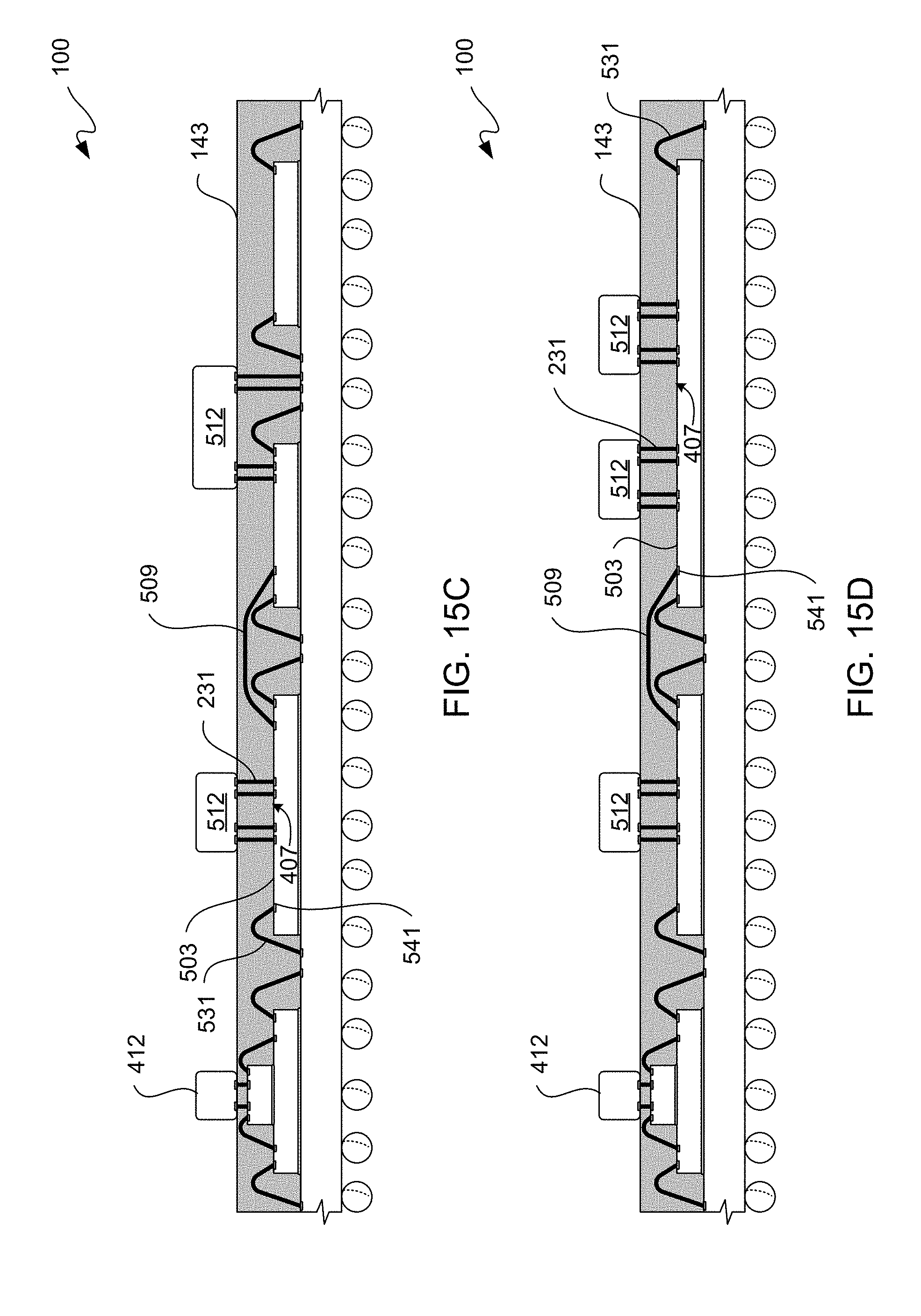
D00018

D00019
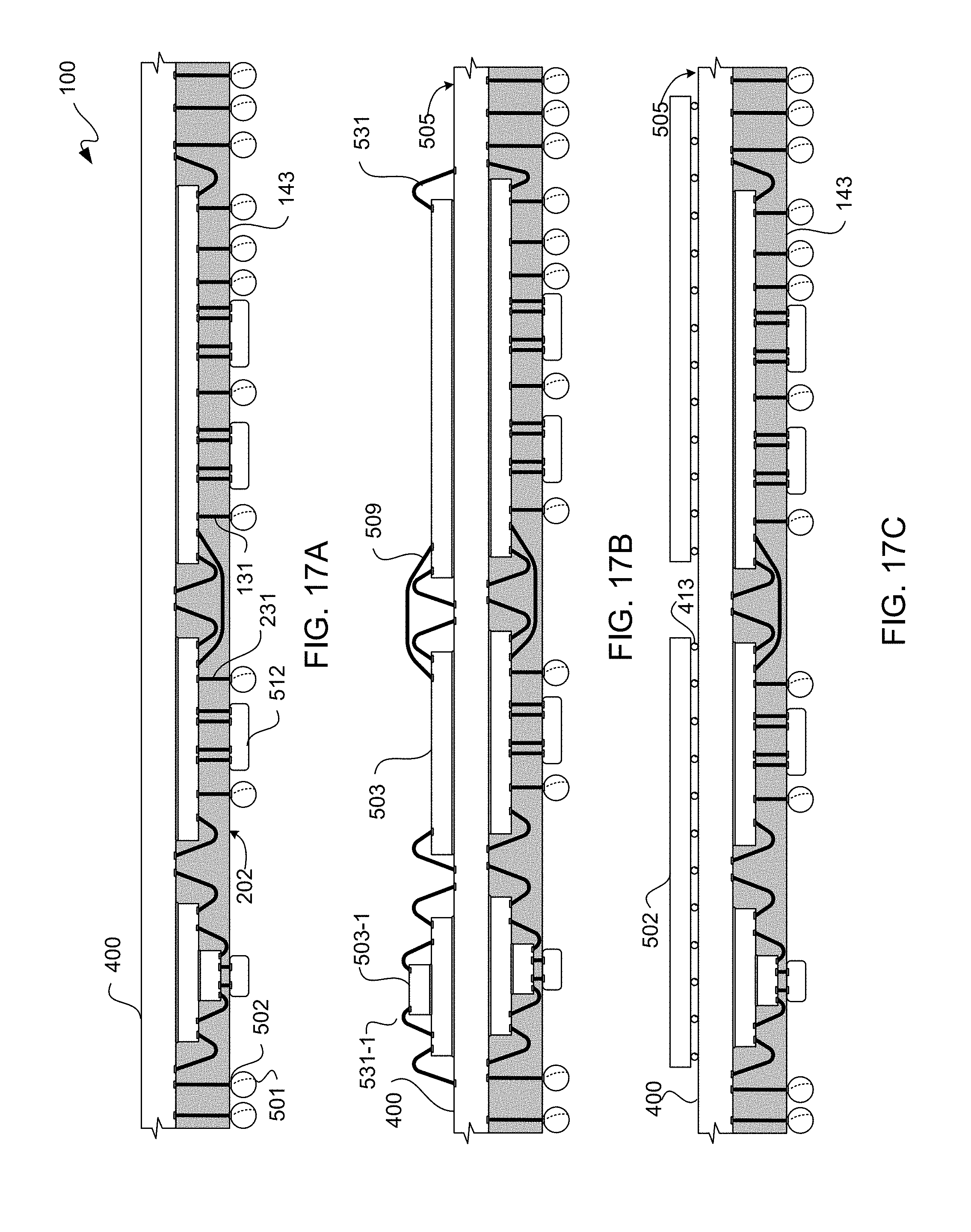
D00020

D00021
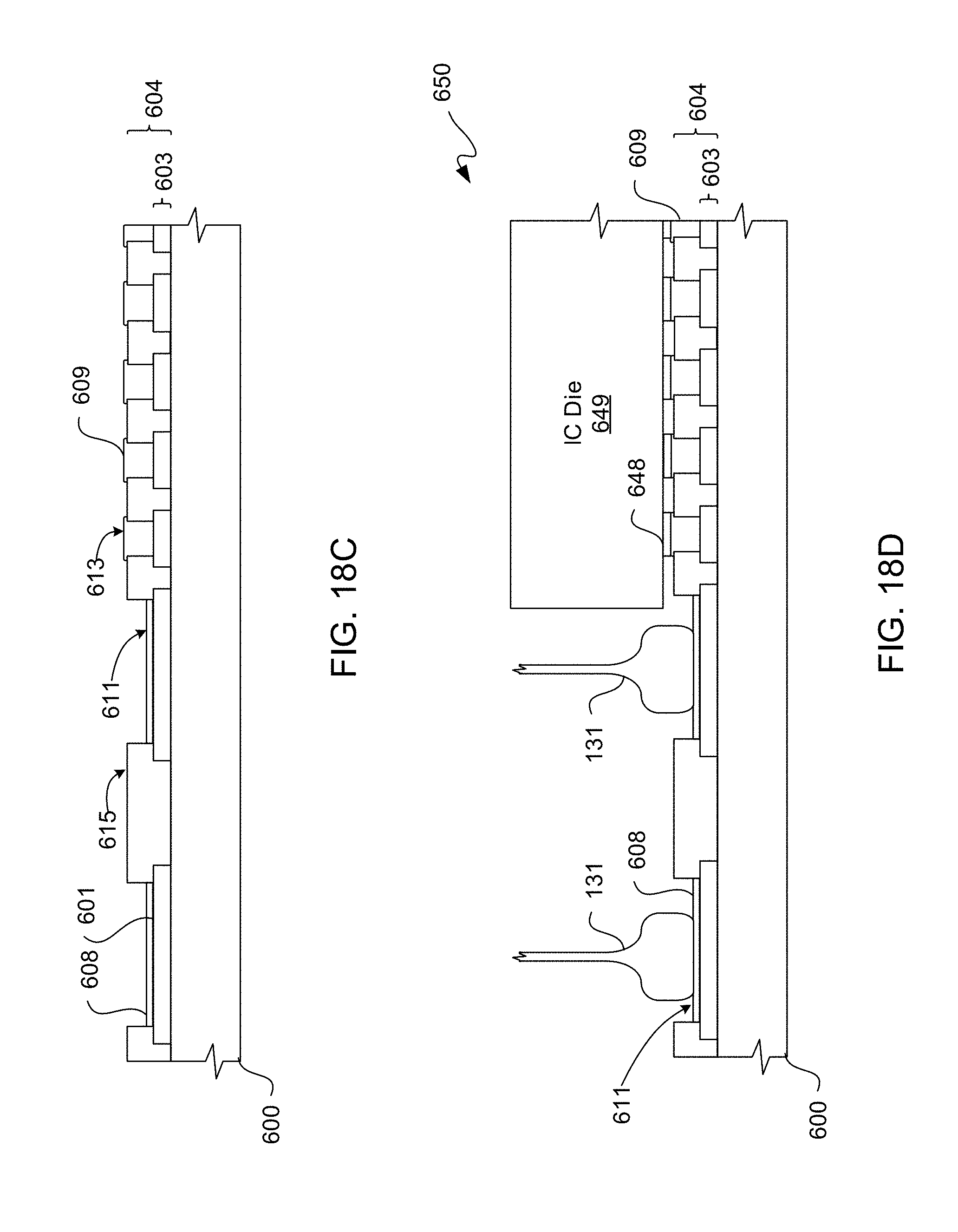
XML
uspto.report is an independent third-party trademark research tool that is not affiliated, endorsed, or sponsored by the United States Patent and Trademark Office (USPTO) or any other governmental organization. The information provided by uspto.report is based on publicly available data at the time of writing and is intended for informational purposes only.
While we strive to provide accurate and up-to-date information, we do not guarantee the accuracy, completeness, reliability, or suitability of the information displayed on this site. The use of this site is at your own risk. Any reliance you place on such information is therefore strictly at your own risk.
All official trademark data, including owner information, should be verified by visiting the official USPTO website at www.uspto.gov. This site is not intended to replace professional legal advice and should not be used as a substitute for consulting with a legal professional who is knowledgeable about trademark law.