Layer Structures For Making Direct Metal-to-metal Bonds At Low Temperatures In Microelectronics
GAO; Guilian ; et al.
U.S. patent application number 16/218769 was filed with the patent office on 2020-03-05 for layer structures for making direct metal-to-metal bonds at low temperatures in microelectronics. The applicant listed for this patent is Invensas Bonding Technologies, Inc.. Invention is credited to Gaius Gillman FOUNTAIN, JR., Guilian GAO, Rajesh KATKAR, Laura Wills MIRKARIMI, Ilyas MOHAMMED, Cyprian Emeka UZOH.
| Application Number | 20200075534 16/218769 |
| Document ID | / |
| Family ID | 69640691 |
| Filed Date | 2020-03-05 |


View All Diagrams
| United States Patent Application | 20200075534 |
| Kind Code | A1 |
| GAO; Guilian ; et al. | March 5, 2020 |
LAYER STRUCTURES FOR MAKING DIRECT METAL-TO-METAL BONDS AT LOW TEMPERATURES IN MICROELECTRONICS
Abstract
Layer structures for making direct metal-to-metal bonds at low temperatures and shorter annealing durations in microelectronics are provided. Example bonding interface structures enable direct metal-to-metal bonding of interconnects at low annealing temperatures of 150.degree. C. or below, and at a lower energy budget. The example structures provide a precise metal recess distance for conductive pads and vias being bonded that can be achieved in high volume manufacturing. The example structures provide a vertical stack of conductive layers under the bonding interface, with geometries and thermal expansion features designed to vertically expand the stack at lower temperatures over the precise recess distance to make the direct metal-to-metal bonds. Further enhancements, such as surface nanotexture and copper crystal plane selection, can further actuate the direct metal-to-metal bonding at lowered annealing temperatures and shorter annealing durations.
| Inventors: | GAO; Guilian; (San Jose, CA) ; FOUNTAIN, JR.; Gaius Gillman; (Youngsville, NC) ; MIRKARIMI; Laura Wills; (Sunol, CA) ; KATKAR; Rajesh; (Milpitas, CA) ; MOHAMMED; Ilyas; (Santa Clara, CA) ; UZOH; Cyprian Emeka; (San Jose, CA) | ||||||||||
| Applicant: |
|
||||||||||
|---|---|---|---|---|---|---|---|---|---|---|---|
| Family ID: | 69640691 | ||||||||||
| Appl. No.: | 16/218769 | ||||||||||
| Filed: | December 13, 2018 |
Related U.S. Patent Documents
| Application Number | Filing Date | Patent Number | ||
|---|---|---|---|---|
| 62725801 | Aug 31, 2018 | |||
| Current U.S. Class: | 1/1 |
| Current CPC Class: | H01L 21/76877 20130101; H01L 24/16 20130101; H01L 24/32 20130101; H01L 24/81 20130101; H01L 24/09 20130101; H01L 24/83 20130101; H01L 2924/01029 20130101; H01L 2924/351 20130101; H01L 23/5226 20130101 |
| International Class: | H01L 23/00 20060101 H01L023/00; H01L 23/522 20060101 H01L023/522; H01L 21/768 20060101 H01L021/768 |
Claims
1. A structure comprising: a first substrate with a bonding surface for bonding to a second substrate; a confinement matrix; a conductive via at least partially confined by the confinement matrix; and a buried metal conductively connected to the conductive via, the buried metal having a width greater than a width of the conductive via and having a vertical thickness between approximately 0.5-1.5 .mu.m.
2. The structure of claim 1, wherein the conductive via has a vertical thickness between approximately 0.6-2.0 .mu.m.
3. The structure of claim 1, wherein the conductive via has a circular horizontal cross-section with a diameter of 5.mu.m or greater.
4. The structure of claim 3, wherein at least part of the buried metal is at least part of a trace, the trace configured to electrically couple the conductive via to an electrical device on or within the first substrate.
5. The structure of claim 3, further comprising a second confinement matrix around at least part of the buried metal to direct thermal expansion of the buried metal vertically.
6. The structure of claim 3, wherein the buried metal further comprises a stack of buried metal layers; each buried metal layer in the stack is surrounded at least in part by the second confinement matrix; each buried metal layer in the stack is conductively connected to the conductive via; and a thermal expansion of each buried metal is capable of increasing a vertical thermal expansion of the conductive via.
7. The structure of claim 6, wherein a CTE of the conductive via is different than the CTE of at least one of the buried metal layers in the stack.
8. The structure of claim 6, wherein the second confinement matrix converts a horizontal thermal expansion of at least one of the buried metal layers into a vertical thermal expansion of the conductive via.
9. The structure of claim 1, further comprising a bump, an inlay, or a layer of an organic material disposed under the buried metal; the bump, inlay, or layer of organic material having a coefficient of thermal expansion (CTE) greater than the CTE of the buried metal.
10. The structure of claim 1, wherein at least a top surface of the conductive via comprises copper metal with lattice planes possessing 111 Miller indices for rapid diffusion of copper atoms during direct metal-to-metal bonding.
11. The structure of claim 1, wherein at least a top surface of the conductive via comprises a nanotexture surface for formation of direct metal-to-metal bonds at an annealing temperature of 150.degree. C. or less.
12. The structure of claim 11, wherein the nanotexture surface comprises a hexagonal network of screw dislocations in a copper metal.
13. A structure comprising: a first substrate with a bonding surface for bonding to a second substrate; a confinement matrix; a conductive via having a vertical thickness between approximately 0.6-2.0 .mu.m; and a buried metal conductively connected to the conductive via and having a horizontal footprint greater than a horizontal footprint of the conductive via, at least part of the buried metal configured to direct thermal expansion of the conductive via vertically.
14. A method, comprising: applying a first confinement matrix to a first substrate; forming a first trench or via in the first confinement matrix; filling the first trench or via with one or more metals having a thickness above the substrate of approximately 0.5-1.5 .mu.m; applying a second confinement matrix onto the first confinement matrix and onto the one or more metals; forming a second trench or via in the second confinement matrix with a smaller cross-section than the first trench or via; at least partly filling the second trench or via with a conductive material in electrical communication with the one or more metals to form a first conductive via having a thickness above the first trench of approximately 0.6-2.0 .mu.m; and planarizing at least the second confinement matrix to create a bonding surface for direct hybrid bonding to a second substrate.
15. The method of claim 14, further comprising joining the bonding surface with the second substrate to create direct contact bonds between the second confinement matrix and the second substrate, the second substrate having a second conductive via.
16. The method of claim 15, further comprising annealing a bonded interface between the first and second substrates after joining at a temperature equal to or less than 150.degree. C. to thermally expand the one or more metals in the first trench or via and the first and second conductive vias on the first and second substrates to create a direct metal-to-metal bond between the first and second conductive vias.
17. The method of claim 14, wherein at least partly filling the second trench or via comprises forming the first conductive via having a cross-section of 5 .mu.m or greater.
18. The method of claim 14, further comprising creating a nanostructure surface on the top surface of the first conductive via to lower the annealing temperature and to shorten a duration of the annealing.
19. An apparatus with a first substrate bonded to a second substrate, each substrate comprising: a semiconductor die; a confinement matrix above the semiconductor die with a bonding surface for bonding to the other substrate; a conductive via within the confinement matrix having a thickness of 0.6-2.0 .mu.m; and a buried metal between the semiconductor die and the conductive via conductively connected to the conductive via and having a horizontal footprint greater than a horizontal footprint of the conductive via, at least part of the buried metal configured to direct thermal expansion of the conductive via vertically.
20. The apparatus of claim 19, wherein each substrate further comprises an embedded bump, inlay, or organic layer between the buried metal and semiconductor die.
Description
[0001] This application claims priority to U.S. Provisional Patent Application No. 62/725,801, filed Aug. 31, 2018, titled "LAYER STRUCTURES FOR MAKING DIRECT METAL-TO-METAL BONDS AT LOW TEMPERATURES IN MICROELECTRONICS," the entire disclosure of which is hereby incorporated herein by reference.
BACKGROUND
[0002] Making electrical connections at bonding interfaces has become paramount in microelectronics, as the transistor density that can be arrayed in a given 2-dimensional area has doubled every 18-24 months, for decades. Conventional flip chip connectors between semiconductor die and circuit board provide 45 contact bump connections per square millimeter (sq. mm), with each connection averaging 180 microns (.mu.m) in bonding pitch. Conventional micropillar connectors improve upon conventional flip chip connectors, providing 625 pillar connections per sq. mm, with each connection averaging 40 .mu.m in pitch. Bond pad width may be considered the size of the conductive pads to be bonded, while pitch refers to the distance between connections. Making 1,000,000 connections per sq. mm requires a bond pitch of 1 .mu.m, for example, with a pad size that is likely around 0.5 .mu.m. For wafer-to-wafer or die-to-wafer bonding that includes electrical interconnects, direct bonding techniques that include direct metal-to-metal bonding, such as "direct bond interconnect" (DBI.RTM. brand) direct hybrid bonding, can provide 100,000-1,000,000 connections per sq. mm, with each connection averaging from <1 .mu.m-40 .mu.m in pitch (Invensas Inc., a subsidiary of Xperi Corp., San Jose, Calif.). Even greater connection density is feasible with connections that are less than 1 .mu.m in pitch.
[0003] Direct hybrid bonding processes, such as DBI.RTM. direct hybrid bonding, presuppose ultra-flat bonding surfaces, and so high density connections to be made by such direct bonding rely on varieties of chemical-mechanical planarization (CMP) processes to make the surfaces to be bonded flat to within a few ten-thousandths of a micron (within a few tenths of a nanometer) over a large surface. Various CMP processes can achieve a depth-of-field flatness sufficient for photolithography, or sufficient for 22 nanometer node technology, for example.
[0004] To achieve such exceptionally fine-pitch 3D electrical interconnects at ultra-high density, the alignment and bonding processes must also be finely tuned. The alignment and dielectric (nonmetal) bonding parts of the direct hybrid bonding process can be performed at room temperature. The dielectric portions of the bonding surfaces (for example, silicon oxide) forms oxide-to-oxide bonding spontaneously when the prepared surfaces are bought together. The metal pads or vias that are confined in the dielectric material, however, are slightly recessed from the dielectric surface that makes up the horizontal bonding interface, such that the metal pads do not impede bonding of the dielectric surfaces upon contact of the dielectric surfaces with each other.
[0005] Conventional annealing stages of direct hybrid bonding processes are at a raised temperature. At these higher annealing temperatures, the metal pads or vias expand vertically more than the surrounding dielectric material, due to the difference in coefficients of thermal expansion (CTEs) between metals and dielectrics. If the recess is sufficiently shallow, the metal vias or pads on each side of the surface being bonded will expand to bridge the small gap between the two metal surfaces and form a physical contact with each other at a certain self-expansion. The oxide-to-oxide bonding of the dielectrics around the metal pads further strengthens at these higher annealing temperatures to allow the metal pads to expand into each other and permanently bond. Bonding between metal pads initiates when copper atoms (for example, for copper pads) at each surface begin to make mutual metallic bonds with other copper atoms on the other side of the interface. No solder or other adhesives are used in the direct hybrid bonding process of electrical interconnects in this manner.
[0006] But the temperatures used in conventional annealing steps for direct hybrid bonding can place thermal stress on ever-smaller semiconductor components used in microelectronics. This annealing temperature could be lowered, but thermal expansion at lower temperatures is limited and requires very precise control of copper pad placement with respect to the recess distance of the metal pads from the bonding interface at room temperature, a precise control that is difficult to achieve in high volume manufacturing. This recess distance results from the CMP step, resulting in a very narrow manufacturing window that is impractical: any slight protrusion of the metal pad above the horizontal plane of the bonding interface composed of the dielectric surface can impede the spontaneous dielectric bonding phase of the direct hybrid bonding process that occurs at room temperature, and this causes overall bonding failure. Structures and processes that could otherwise lower the annealing temperature for direct metal-to-metal bonding of interconnects are desirable for further progress in 3D semiconductor packaging.
SUMMARY
[0007] Layer structures for making direct metal-to-metal bonds at low temperatures and shorter annealing duration in microelectronics are provided. Example bonding interface structures enable direct metal-to-metal bonding of interconnects at low annealing temperatures of 150.degree. C. or below, and at a lower energy budget due to shorter annealing times. The example structures provide a precise metal recess distance for conductive pads and vias being bonded that can be achieved in high volume manufacturing. The example structures provide a vertical stack of conductive layers confined by a surrounding dielectric with geometries and thermal expansion features designed to vertically expand the stack over the precise recess distance at lower temperatures to make the direct metal-to-metal bonds at the bonding interface without solders or adhesives. Further enhancements, such as surface nanotexture and copper crystal plane selection, can further actuate the direct metal-to-metal bonding at lowered annealing temperatures and shorter annealing durations.
[0008] This summary is not intended to identify key or essential features of the claimed subject matter, nor is it intended to be used as an aid in limiting the scope of the claimed subject matter.
BRIEF DESCRIPTION OF THE DRAWINGS
[0009] Certain embodiments of the disclosure will hereafter be described with reference to the accompanying drawings, wherein like reference numerals denote like elements. It should be understood, however, that the accompanying figures illustrate the various implementations described herein and are not meant to limit the scope of various technologies described herein.
[0010] FIG. 1 is a diagram of an example layer structure suitable for making direct metal-to-metal bonds at low annealing temperatures and short annealing durations in microelectronics.
[0011] FIG. 2 is a diagram of an example device with example layer structure for making direct metal-to-metal bonds, including a recess distance for bonding pads obtainable in high volume manufacturing.
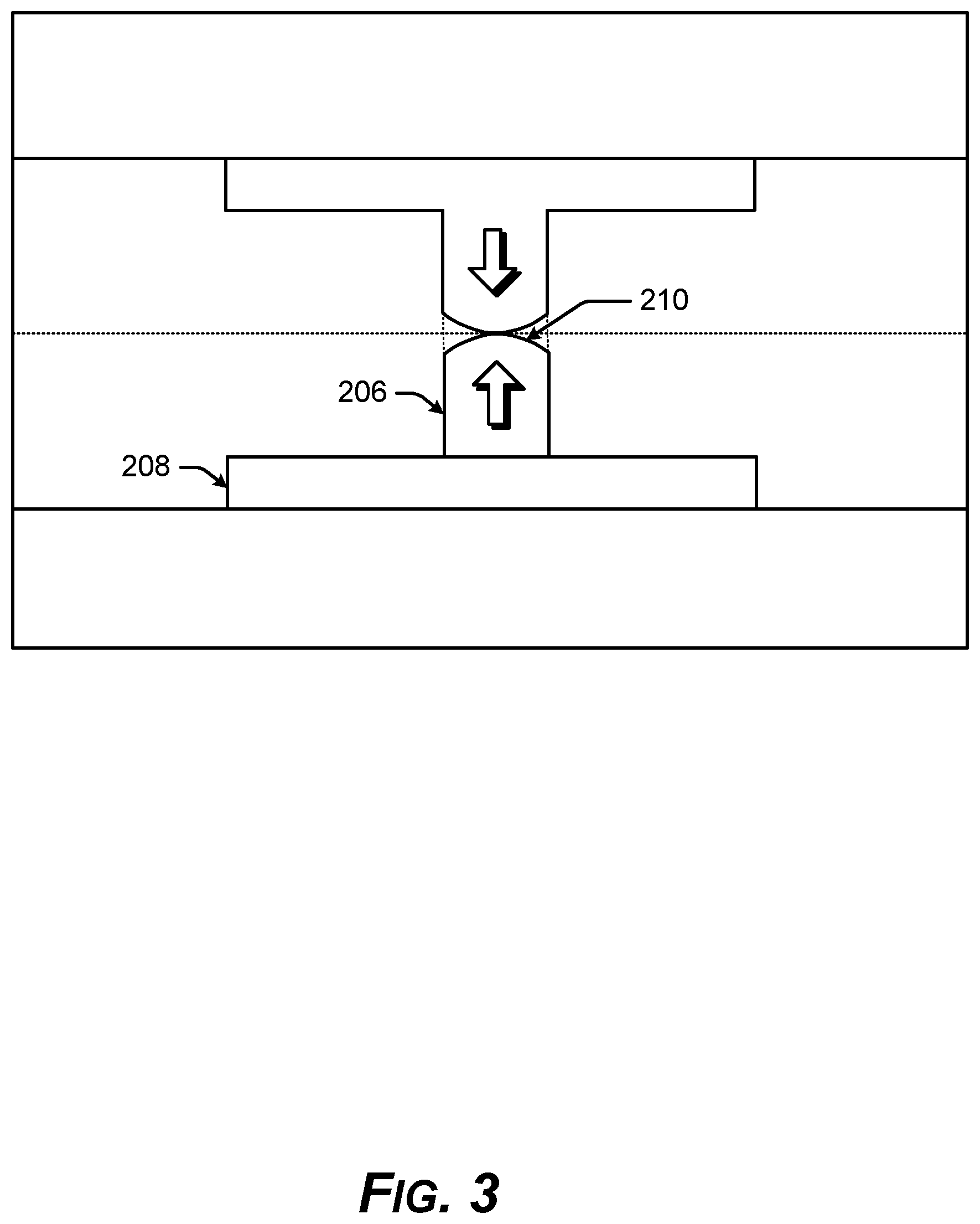
[0012] FIG. 3 is a diagram showing a geometry of thermal expansion of a metal bonding surface for direct metal-to-metal bonding.
[0013] FIG. 4 is a diagram plotting maximum recess distances from a bonding plane versus temperatures, for different thicknesses of a thermally expanding metal contact.
[0014] FIG. 5 shows two example diagrams of three conductive layers with respective CTE's within vertical direct-bonding stacks.
[0015] FIG. 6 shows a buried metal bump or inlay of an organic material with high CTE providing vertical thermal expansion to lower annealing temperature and shorten annealing durations during an example direct hybrid bonding process.
[0016] FIG. 7 is a diagram showing multiple parallel vias as either a first conductive layer or second conductive layer in direct metal-to-metal bonding.
[0017] FIG. 8 is a diagram showing an example process flow for creating a bonding interface structure that enables direct metal-to-metal bonding with lower annealing temperatures and shorter annealing time than conventionally used.
[0018] FIG. 9 is a diagram showing instances of the structures formed in FIG. 8 being joined in an example direct hybrid bonding process.
[0019] FIG. 10 is a diagram showing an example process of making a nanotextured surface to lower annealing temperatures and shorten annealing time in direct metal-to-metal bonding.
[0020] FIG. 11 is a flow diagram showing an example process for making a structure suitable for forming direct metal-to-metal bonds at low annealing temperatures and short annealing durations.
DETAILED DESCRIPTION
[0021] Overview
[0022] This disclosure describes layer structures for making direct metal-to-metal bonds at low temperatures and short annealing durations in microelectronics. Example bonding interface structures enable direct metal-to-metal bonding of interconnects at low annealing temperatures of 150.degree. C. or below. The example structures provide a precise metal recess specification of 4-6 nanometers, for example, that can be achieved in high volume manufacturing. In direct hybrid bonding, direct bonding of dielectric surfaces occurs first across a bonding interface. Then, in an anneal stage, the recessed vias or pads at the precise recess distance can expand at a low annealing temperature and shorter annealing duration to bridge the gap and form direct metal-to-metal bonds.
[0023] Reducing the energy budget or "thermal budget" for creating direct hybrid bonds, including metal-to-metal bonding of conductive interconnects, includes not only lowering annealing temperatures but also lowering the duration of the annealing phase of hybrid bonding. Example techniques are also described herein for shortening the annealing duration.
[0024] Significantly, example structures enabling direct hybrid bonds to be formed at a reduced energy budget allow hundreds-of-thousands or even over one-million electrical interconnects per square millimeter to be completed at lower temperatures and lower energy budget than temperatures conventionally applied in direct hybrid bonding of metal interconnects. Direct bonding can be accomplished either through thermal compression bonding or hybrid bonding. Hybrid bonding is described herein as an example. The example low-temperature processes are safer for semiconductor components and fabrication apparatuses, and also less expensive to implement. The example low-temperature processes also enable application of direct hybrid bonding to components and products that cannot be annealed at conventional annealing temperatures of 250.degree. C. and above.
Example Bonding Interface Structures
[0025] Low-temperature direct metal-to-metal bonding is attractive for some applications. But the vertical thermal expansion needed to bond metals together in direct hybrid bonding processes is limited at lower temperatures compared with the vertical thermal expansion achievable at those annealing temperatures used conventionally, triggering a need for precise control of the structure of the bonding interface before the bonding can occur at the lower temperatures.
[0026] Specifically, as shown in FIG. 1, performing direct hybrid bonding at lower temperatures requires careful control of how far the metal pads 100 & 100' to be bonded can be recessed from the bonding interface plane 102 itself. This retraction of the metal pads 100 & 100' from the plane of the larger bonding interface 102 is known herein as the "maximum recess distance" 104 or just "recess" 104, and ranges from 0 nanometers (nm) to the maximum recess allowed. Protrusion of a metal pad 100 above the horizontal plane 102 before the annealing step is generally not allowed or not preferred. In turn, the lower tolerances imposed on this recess parameter 104 to achieve lower annealing temperatures, trigger a need for careful control of chemical-mechanical planarization (CMP) operations for flattening dies and wafers, which establish the plane of the bonding interface 102 and the resulting recess distance 104 of metal contacts in the first place.
[0027] In an implementation, to enable direct bonding of metal interconnects at low temperatures, the maximum recess distance 104 between the metal pads 100 that are to be bonded and the horizontal plane of the larger bonding interface 102 is designed to be only a few nanometers (per side), and the metal pads 100 and structures 106 underlying the metal pads 100 are designed to expand with a calculated thermal expansion sufficient to raise each metal pad 100 into an opposing metal pad 100' belonging to the other surface being joined, in order to direct-bond the metal pads 100 & 100' into a single metal interconnect 110 after the bond. The maximum recess distance 104 between each metal pad 100 and its respective larger bonding interface 102 or 102' is critical for achieving low-temperature direct bonding. If the specification for recess distance 104 is too small, for example, then control of the CMP process control is difficult and the risk of having the metal pad 100 protrude above the dielectric surface 102 increases. If the metal pads 100 are slightly higher than the larger bonding interface 102, then no dielectric bonding in layer 108 occurs around the protruded pads. If a sufficient number of the protruded pads disrupt bonding of the surrounding larger dielectric surface 102, bonding failure occurs.
[0028] On the other hand, if the recess distance 104 is too large, then the metal pads 100 & 100' do not expand enough at the lower annealing temperature to make contact at the bonding interface 102, once thermal expansion of the metal pads 100 and the underlying structures 106 is spent. This results in oxide-to-oxide bonding of the nonmetal parts 108 of the bonding interface 102, but no bonding of the metal pads 100 & 100', since the metal pads 100 & 100' never make contact with each other across the bonding interface 102. The dielectric surfaces bond, but with no electrical interconnects across the joined surfaces.
[0029] When copper is the metal being direct-bonded, higher temperatures of an annealing step can actuate changes in grain-size for the copper metal on each side of the metal-to-metal bond. This too can be reckoned favorably into low-temperature direct bonding. Likewise, the metal surfaces 100 to be bonded can be intentionally modified to favor bonding at lower temperatures. Conventionally, the CMP process presents surfaces of pure materials, at which metal areas of the flattened surface are free of oxides and impurities. The bonding surface can be activated with plasma, to decrease activation energy for forming bonds and to create some disruption in charge balances at the surface that favors bond formation. In an implementation herein, metal pads 100 to be direct-bonded as interconnects may also be topped by creating nanoparticles of the metal on the bonding surface, to increase the bonding surface area exponentially and physically catalyze or seed metallic direct-bonding. In another implementation, selection of a copper crystal plane increases the rate that copper atoms diffuse across the bonding interface to form permanent metal-to-metal bonds, thereby enabling a reduced annealing temperature and shorter annealing durations.
[0030] FIG. 2 shows an example layer structure 200 in a microelectronic device in which a metal pad 100 is recessed a distance 104 from the plane of a bonding interface 102. The recess distance 104 is not to scale in FIG. 2, and is shown greatly exaggerated for descriptive purposes. The dielectric layer 108 of the bonding interface 102 has a surface in a horizontal plane. A via 202 is disposed vertically in the horizontal surface of the dielectric layer 108. A vertical stack 204 of conductive layers 206 & 208 resides in the via 202. The conductive layers 206 and 208 may have more than one metal composition and each conductive layer 206 & 208 in the vertical stack 204 has a respective coefficient of thermal expansion (COE), labeled .alpha.1 & .alpha.2.
[0031] From the horizontal surface of the bonding interface 102, the recess distance 104 of the top surface 210 of the first conductive layer 206 in the vertical stack 204 varies by temperature, because the conductive layers 206 & 208 expand or contract in relation to the temperature. For a given layer structure 200, the recess distance 104 at room temperature has a specific range for a given annealing temperature for direct metal-to-metal bonding. The recess is dependent on the volume and geometry of the two conductors 206 & 208 in the vertical stack 204, and their respective coefficients of thermal expansion .alpha.1 & .alpha.2.
[0032] In an implementation, at an annealing temperature below conventional annealing temperatures around 250.degree. C., the vertical stack 204 thermally expands so that at least part of the top surface 210 of the first conductive layer 206 expands or bulges over the recess distance 104 to the horizontal surface of the bonding interface 102, putting the top surface 210 in position for making a direct metal-to-metal bond at the bonding interface 102 with another instance of a vertical stack 204 on the other side of the bonding interface. The actual annealing temperature may be between 150-200.degree. C., or may be around 150.degree. C., or may even be below 150.degree. C. These approximate temperatures are much lower than conventional temperatures around 250.degree. C. needed for the anneal step in direct hybrid bonding.
[0033] In this implementation, the second conductive layer 208 of the vertical stack 204 resides below the first conductive layer 206 and is conductively connected to the first conductive layer 206. The second conductive layer 208 may have a second coefficient of thermal expansion .alpha.2.
[0034] At least one bottom layer 212 beneath the vertical stack 204 consists of the material of a semiconductor die or wafer, or a substrate material, such as glass, dielectric, conductor, etc.
[0035] The dielectric confinement layer 108, such as silicon dioxide, provides a confinement matrix around the vertical conductive stack 204, and has substantially lower CTE than the metal stack 204 in order to provide substantial confinement of horizontal expansion forces of the metal stack 204 and thereby generate substantial vertical expansion in the buried conductive layer 208. The dielectric layer 108 is rigid enough to substantially constrain most expansion of the vertical stack 204 to within the vertical stack 204 itself. Thus, by confining expansion forces, the dielectric layer 108 transforms horizontal thermal expansions of the first conductive layer 206 and the second conductive layer 208 into vertical expansion within the vertical stack 204. Example processes for building the dielectric layer(s) 108 and example vertical conductive stacks 204 are described below, with respect to FIG. 8, for example.
[0036] As shown in FIG. 3, the combined vertical thermal expansion of the first conductive layer 206 and the second conductive layer 208 expand the top surface 210 so that at least a part of the top surface 210 of the first conductive layer 206 bulges, deforms, expands, and/or moves across the recess distance 104 up to the horizontal surface of the bonding interface 102 at an annealing temperature around approximately 150.degree. C. or below.
[0037] Referring again to FIG. 2, the dielectric layer 108, when made of silicon dioxide for example, has a coefficient of thermal expansion (CTE) of approximately 0.55.times.10.sup.-6/.degree. C. and a hardness of 7 Mohs. In some implementations, other materials may be used for the dielectric 108. A suitable dielectric 108 may have a CTE equal to or greater than that of silicon dioxide, for example, which has a very low CTE.
[0038] In an implementation, the maximum recess distance 104 is determined as in Equation (1), by:
.delta.=.alpha.*.times.h.times..DELTA.T (1)
wherein .delta. is the recess distance 104, .alpha.* is an effective CTE of the vertical stack 204 of conductive layers 206 & 208, h is a thickness of the vertical stack 204 of conductive layers 206 & 208, which consist of three components: .alpha.*.sub.1, .alpha.*.sub.2, and .alpha.*.sub.3, and .DELTA.T is the temperature change between the room temperature and the annealing temperature.
.alpha.*=.alpha.*.sub.1+.alpha.*.sub.2+.alpha.*.sub.3. (2)
[0039] The first component (.alpha.*.sub.1) of the effective CTE .alpha.* of the entire vertical stack 204 of conductive layers 206 & 208 represent the vertical component of thermal expansion of the stack 204 and can be approximated by a composite CTE of the vertical stack 204 of the layers 206 & 208. The composite CTE of the vertical stack 204 can be determined in Equation (2), by:
.alpha.*.sub.1=.alpha.1.times.h1/(h1+h2)+.alpha.2.times.h2/(h1+h2) (3)
where .alpha.1 is the CTE of the first conductive layer 206 of the vertical stack 204, .alpha.2 is the CTE of the second conductive layer 208 of the vertical stack 204, h1 is the thickness 214 of the first conductive layer 206, and h2 is the thickness 216 of the second conductive layer 208. The total thickness of metal in the stack 204, consisting of the first conductive layer 206 and the second conductive layer 208 and any optional additional layers, increases the thermal expansion beyond what can be achieved without a stacked structure, such as having only the first conductive layer 206. The combined thickness h=h1+h2 of the metal stack 204 is greater than thickness h1 of the first conductive layer 206 alone, and therefore lowers the annealing temperature for a given value of the metal recess distance 104.
[0040] The second component (.alpha.*.sub.2) of the effective CTE .alpha.* of the entire vertical stack 204 is the contribution (.alpha.*.sub.2) of the horizontal expansion of the second buried metal layer 208, which is converted to vertical expansion because of confinement by the dielectric 108. When the horizontal footprint of the buried metal layer 208 is larger than that of the first buried conductive layer 206 above it, the .alpha.*.sub.2 contribution is even more significant.
[0041] The third component of the effective CTE .alpha.* of the vertical stack 204 (.alpha.*.sub.3) is related to the surface area .phi.1 of the top surface 210 of the first conductive layer 206, this surface 210 can be the metal "pad" to be bonded. The movement of the outer edge of conductive layer 206 is constrained by the dielectric confinement matrix 108, since the two are adjacent. During design, increasing the surface area of the top surface 210 of the first conductive layer 206 provides less constraint to thermal expansion in the volume of metal within the first conductive layer 206 that is further away from the interface between the first conductive layer 206 and the constraining dielectric matrix 108. Consequently, at a given annealing temperature, the center portion of the top surface 210 on a large metal pad or conductive layer 206 expands further compared to a small pad with a small top surface 210. This contribution to the effective CTE .alpha.*.sup.of the entire vertical stack 204 is captured with .alpha.*.sub.3 as in Equation (2).
[0042] Structural designs, for example direct metal-to-metal bonding, that incorporate the following features and parameters can substantially reduce the annealing temperature of conductive vias 206 with example recesses 104 greater than 1-2 nm, to below 200.degree. C., and even below 150.degree. C. An example structure has a thick upper metal via 206, with h1 thicker than 0.5 .mu.m for example, in an example range of 0.6-2.0 .mu.m. The upper metal via 206 is conductively conducted to one or more buried metal layers 208, such as one or more trace layers of the BEOL stack layer, to increase effective total stack thickness h 204. When the buried metal layer 208 consists of part of a trace, the buried metal layer 208 can be intentionally thicker than usual trace layers, for example, in the range of 0.5-1.5 .mu.m. The example buried metal layer 208 has a larger footprint (horizontal cross-section) than the via layer 206 above it. The larger than usual top surface area 210 of the upper via 206 also enables a lower annealing temperature for forming metal-to-metal bonds. For example, a conventional circular upper via 206 has a 3 .mu.m diameter top surface 210, while an example enlarged upper via 206 as described herein for lowering the annealing temperature may have an upper circular pad surface 210 with a 5 .mu.m, 10 .mu.m, or 15 .mu.m diameter.
[0043] FIG. 4 is a diagram plotting theoretical calculation of differential thermal expansion between Cu metal 206 and the dielectric SiO.sub.2 108 (i.e., the minimum annealing temperature) as a function of annealing temperature and h1 metal thickness 214 using the .alpha.*.sub.1 component (vertical thermal expansion) of the overall effective CTE .alpha.*. For a given metal thickness 214, if the combination of annealing temperature and metal recess 104 falls below the respective visual line on the plot, the two metal surfaces theoretically will not expand into contact with each other to form a metal-to-metal bond. If the combination falls above the line, metal-to-metal bonding will theoretically happen.
[0044] For a given annealing temperature, the larger the metal recess distance 104, the higher the annealing temperature that is required. The smaller the recess distance 104, the lower the required annealing temperature that is required for a metal-to-metal bond to occur. However, for CMP process control and high-volume manufacturing, a very small recess specification is not desirable. By increasing the total metal thickness h1 214 below the via surface 210, the slope of the line gets smaller in the plot, and then for a given recess 104, the calculated annealing temperature is lower with the greater total thickness 214 of the upper metal via 206.
[0045] The impact of the metal thickness 214 and other dimensions is demonstrated with the following example. For a 3 .mu.m diameter via 206 with a 6 nm recess distance 104, if the upper metal via 206 has a vertical thickness (h1) 214 of 0.8 .mu.m and the buried trace 208 that the upper metal via 206 is connected to has a vertical thickness (h2) 216 of 0.2 .mu.m for a total metal h thickness 204 of 1.0 .mu.m, then the calculated annealing temperature is close to 300.degree. C. But when the buried metal trace 208 (which can be more than one layer) is increased to 0.8 .mu.m to give a total metal stack thickness (h) 204 of 1.6 .mu.m, then the calculated annealing temperature is reduced to 180.degree. C. When the upper via layer 206 is increase to 1.3 .mu.m for a total metal stack thickness (h) 204 of 2.1 .mu.m, then the calculated annealing temperature is reduced to 130 C. Further increases in the metal stack thickness (h) 204 can further decrease the calculated annealing temperature.
[0046] As above, changing the metal recess distance parameter 104 lowers the annealing temperature. Given a total metal stack thickness (h) 204 of 1.6 .mu.m, reducing the Cu recess distance 104 from 6 nm to 4 nm reduces the calculated annealing temperature from a nominal 180.degree. C. to 121.degree. C.
[0047] In an implementation, with proper design and combination of materials to optimize confinement by the dielectric 108, the contribution of components .alpha.*.sub.2 (horizontal thermal expansion converted to vertical) and .alpha.*.sub.3 (surface area of the metal-to-metal bonding surface) of the overall effective CTE reduces the annealing temperature to below even the calculated value. As shown above, with a metal stack thickness (h) of 1.6 .mu.m, the calculated minimum annealing temperature using the example parameter for the .alpha.*.sub.1 component alone is 180.degree. C., a great improvement over conventional annealing temperatures in direct hybrid bonding. Successful metal-to-metal bonding at lower annealing temperatures have been demonstrated with a total Cu stack thickness (h) 204 of 1.6 .mu.m at 150.degree. C. versus a 180.degree. C. calculated value from using an improved .alpha.*.sub.1 (vertical thermal expansion) component alone, due to additional contributions from .alpha.*.sub.2 (horizontal thermal expansion converted to vertical) and .alpha.*.sub.3 (surface area of the top of metal via or pad being bonded).
[0048] In an implementation, a copper first conductive layer 206 has a vertical thickness (h1) 214 of 1.6 .mu.m, and a CTE .alpha.1 that is in a range of 16.7-17.0.times.10.sup.-6/.degree. C. The second conductive layer 208 is also copper with a vertical thickness (h2) 216 which may also be around 0.5-1.0 .mu.m, and a CTE .alpha.2 that is also in the range of 16.7-17.0.times.10.sup.-6/.degree. C. In this scenario, the maximum recess distance .delta. is approximately 6 nanometers (nm), and the annealing temperature is lowered down to between 150-200.degree. C.
[0049] The second "buried metal" conductive layer 208 of the vertical stack 204 may be at least in part, a part of a redistribution layer (RDL) or an electrical trace of the microelectronic component being fabricated. In an implementation, the RDL or electrical trace making up the second conductive buried metal layer 208 has a horizontal footprint with at least one dimension greater than a corresponding horizontal dimension of the footprint of the first conductive layer 206. The greater footprint of the underlying second conductive layer 208 compared to the first conductive layer 206 provides more thermal expansion through a greater volume of metal, including its horizontal thermal expansion converted to vertical expansion of the vertical stack 204 because of the confinement of horizontal expansion provided by the dielectric confinement matrix 108. This increase in the volume of metal buried deeper beneath the bonding interface 102 and below the first metal via 206 is significant, since only a few nanometers in recess distance 104 lowers the temperature needed for annealing that results in direct metal-to-metal bonds.
[0050] Besides pure copper, in a wide variety of implementations, the first conductive layer 206 or the second conductive layer 208 of the vertical stack 204 may be another material, such as a brass alloy with a CTE in a range of 18-19.times.10.sup.-6/.degree. C., a manganese bronze alloy with a CTE of 21.2.times.10.sup.-6/.degree. C., an aluminum metal or aluminum alloy with a CTE in a range of 21-24.times.10.sup.-6/.degree. C., a zinc metal or zinc alloy with a CTE in a range of 30-35.times.10.sup.-6/.degree. C., nickel in copper, for example, or another suitable conductor.
[0051] FIG. 5 shows other example layered structures 500 & 500' for making direct bonds at low annealing temperatures in microelectronics. In these implementations, the vertical stack 502 may also include a third buried conductive layer 504 of the vertical stack 204, either between the second conductive layer 208 and the bottom layer 212 as in structure 500, or between the first conductive layer 206 and the second conductive layer 208 as in structure 500', for example. Although this example has three conductive layers in the vertical stack 502, the vertical stack 502 may contain up to twelve different layers, for example. Moreover, the layers may have various widths and thicknesses to optimize the metal expansion effect.
[0052] The third conductive layer 504 increases the total stack thickness (h) 502 and may increase the effective CTE .alpha.* by providing a conductor in the vertical stack 502 with a higher CTE than copper metal, for example, thereby providing greater vertical thermal expansion of the entire vertical stack 502, which lowers the annealing temperature needed to form direct metal-to-metal bonds in direct hybrid bonding. The geometry of the third conductive layer 504 may also increase both vertical expansion and effective CTE .alpha.* when the horizontal footprint is relatively large, as in structure 500'. Then the horizontal thermal expansion of the third conductive layer 504 at the annealing temperature tends to be converted to additional vertical expansion of the vertical stack 502 because of the constraining dielectric matrix 108. The third conductive layer 504 may be, for example, a brass alloy with a CTE in a range of 18-19.times.10.sup.-6/.degree. C., a manganese bronze alloy with a CTE of 21.2.times.10.sup.-6/.degree. C., an aluminum metal or aluminum alloy with a CTE in a range of 21-24.times.10.sup.-6/.degree. C., a zinc metal or zinc alloy with a CTE in a range of 30-35.times.10.sup.-6/.degree. C., or other suitable conductor.
[0053] The example vertical stacks 502 in FIG. 5 may be confined on at least 3 sides (for example, a trace has the bottom and two sides constrained, the top surface connects to the via 206. All sides adjacent to barrier layers or hardened barrier material or confining dielectric matrix 108 further contain sideways and horizontal expansion forces, converting these forces to vertical expansion forces as their temperature approaches the annealing temperature, expanding the top surface 210 of the first conductive via 206 to the level of the bonding interface 102. This confinement leading to increased vertical expansion lowers the annealing temperature needed to form metal-to-metal bonds in direct hybrid bonding.
[0054] In an example implementation, the first conductive layer 206, which is the direct bonding layer, has a top surface 210 with dimensions of a circular via 5 .mu.m in diameter. The diameter may also be 2 .mu.m, 3 .mu.m, 5 .mu.m, 10 .mu.m and 15 .mu.m, and other sizes, for example. The vertical thickness (h1) of the first conductive layer 206 can be approximately 1.5 .mu.m, and the second conductive layer 208, which may be an RDL layer, has dimensions of 20 .mu.m.times.20 .mu.m.times.0.5 .mu.m, for example. In this example, the metal volume of the first conductive layer 206 is 2.5 .mu.m.times.2.5 .mu.m.times.3.14.times.1.5 .mu.m=29 .mu.m.sup.3, for example. The volume of the second conductive layer 208 is 200 .mu.m.sup.3, for example. The buried metal volume of the second conductive layer 208 is approximately 7 times that of the first conductive layer 206. Even if only a fraction of horizontal thermal expansion of the second conductive layer 208 is deformed to vertical expansion of the first conductive layer 206, this additional expansion significantly increases the effective CTE .alpha.* and substantially reduces annealing temperature for the metal-to-metal bonding.
[0055] In another example, the volume of the first conductive layer 206 is 265 .mu.m.sup.3, for example, and the volume of the "buried" second conductive layer 208 is 327 .mu.m.sup.3, for example. In this case, the contribution of thermal expansion from the layer 206 and layer 208 is approximately same magnitude assuming that the two layers have the same CTE.
[0056] FIG. 6 shows another example layered structure 600 for making direct bonds at low temperatures in microelectronics. In this implementation, the vertical stack 602 may also include an embedded bump 604 or an inlay 606 made of a conductor, or other material, with a higher CTE than copper metal for adding additional thermal vertical expansion to the vertical stack 602. The embedded bump 604 or inlay 606 may be a material such as a brass alloy with a CTE in a range of 18-19.times.10.sup.-6/.degree. C., a manganese bronze alloy with a CTE of 21.2.times.10.sup.-6/.degree. C., an aluminum metal or aluminum alloy with a CTE in a range of 21-24.times.10.sup.-6/.degree. C., a zinc metal or zinc alloy with a CTE in a range of 30-35.times.10.sup.-6/.degree. C., or other suitable metal or non-metal material.
[0057] The embedded bump 604 or inlay 606 can also be a dielectric material, such as an organic material (nonmetal) with a very high CTE, as long as the bump 604 or inlay 606 does not block an electrical conduction path, for example between an electrical trace and the via 206 with the top surface 210 forming the direct metal-to-metal bond. The organic material with high CTE can also be a buried layer, such as layer 504 in structure 500 of FIG. 5, as long as the buried layer 504 does not block an electrical conduction path. The organic material with high CTE for the buried layer 504 or the embedded bump 604 or inlay 606 may be a polyimide with a CTE in a range of 30-60.times.10.sup.-6/.degree. C., an epoxy with a CTE in a range of 45-65.times.10.sup.-6/.degree. C., a chlorinated polyvinylchloride CPVC with a CTE in a range of 63-66.times.10.sup.-6/.degree. C., a phenolic resin with a CTE in a range of 60-80.times.10.sup.-6/.degree. C., a nylon with a CTE in a range of 50-90.times.10.sup.-6/.degree. C., an ABS thermoplastic with a CTE in a range of 22-108.times.10.sup.-6/.degree. C., a polybutylene with a CTE in a range of 130-139.times.10.sup.-6/.degree. C., an ethylene vinyl acetate with a CTE of 180.times.10.sup.-6/.degree. C., and an ethylene ethyl acrylate with a CTE of 205.times.10.sup.-6/.degree. C.
[0058] Referring to FIGS. 2, 5, and 6, the thickness (h1) 214 of the first conductive layer 206 may be increased proportionately to greater than the example nominal 1.6 .mu.m vertical dimension, at a recess distance 104 of 6 nm, in order to lower the annealing temperature further below a nominal temperature of 200.degree. C. for the anneal step of direct hybrid bonding. The greater thickness (h1) 214 for the first conductive layer 206 provides proportionately greater vertical thermal expansion of the vertical stack 204, enabling the same amount of vertical expansion at a lower temperature as provided by a lesser thickness 214 of the first conductive layer 206 at a higher temperature.
[0059] FIG. 7 shows additional example layered structures 700 & 702 for making direct bonds at low temperatures in microelectronics. In an implementation, multiple parallel conductive vias 704 & 706 & 708 make up the first conductive layer 206, and are each surrounded by the dielectric confinement material 108, over a single second conductive layer 208. The first conductive layer 206 is the direct-bonding layer, with top surfaces 210 recessed from the dielectric oxide surface 709. The multiple parallel conductive vias 704 & 706 & 708 each conductively couple to the single second conductive layer 208, which may be an RDL (redistribution layer). The multiple parallel conductive vias 704 & 706 & 708 in the first conductive layer 206 provide multiple bonding opportunities for the same connection to increase yield and reliability through redundancies.
[0060] In another implementation, the example structure 702 in FIG. 7 includes a second conductive layer 208 that has multiple parallel conductive vias 712 & 714 & 716 surrounded by the dielectric confinement filler 108, beneath the single first conductive layer 206. The second conductive layer 208, including the multiple parallel conductive vias 712 & 714 & 716, may be an RDL (redistribution layer) on a die or wafer. The multiple parallel conductive vias 712 & 714 & 716 each conductively couple to the single first conductive layer 206, which is the direct-bonding metal layer with large area top surface 210. This arrangement provides a greater direct-bonding surface area .phi.1 than a single via for direct-bonding, and also enables the direct metal-to-metal bonding to occur at lower temperatures than conventionally used for the annealing step because of the greater surface area .phi.1 of the top surface 210, which can enable the center of the large top surface 210 to deform upward more than the edges of the large top surface 210.
[0061] FIG. 8 shows an example process flow 800 for creating a bonding interface structure, such as structure 500 in FIG. 5, for example, that enables direct metal-to-metal bonding with lower annealing temperatures and shorter annealing times than conventionally used. Steps of the example process flow are shown as individual blocks and corresponding diagrams.
[0062] At block 802, a dielectric material 804 is formed or deposited on a semiconductor or other substrate 806, and trenches 808 are formed in the dielectric material 804 for confining one or more metal layers. The trenches may be etched trenches and/or damascene cavities, for example.
[0063] At block 810, a barrier layer and/or adhesion layer and metal seed layer are applied at least in the trenches 808 for metal deposition. The trenches 808 are then filled with one or more metals 812 & 814, in one or more layers, or can be filled with any other multiple layer composition. The top surface 816 of the metal or metals is flattened with a CMP process to remove excess deposition.
[0064] At block 818, another layer of dielectric material 820 is deposited, and trenches 822 formed or etched for confining a bonding layer metal 824 ("conductive via") to be added next. The trenches 822 are filled with the bonding layer metal 824, and planarized with CMP to remove the excess deposition. The finished surface 826 after CMP meets the dielectric surface roughness and metal recess 104 specification for an example direct hybrid bonding process.
[0065] In FIG. 9, the process of FIG. 8 continues, with instances of the structures and bonding surfaces fabricated in FIG. 8 joined in an example direct hybrid bonding process.
[0066] At block 828, two instances of the bonding interface structure are bonded together in a first phase of a direct hybrid bonding process. The first phase direct-bonds the oxide surfaces 830 of the inorganic dielectrics together. The joining of surfaces may be in a wafer to wafer (W2W) process, a die-to-wafer (D2W) process, or a die-to-die (D2D) process.
[0067] At block 832, the bonded structure is annealed, in a second phase of the direct hybrid bonding process. The raised temperature of the annealing process vertically expands the buried metals 812 & 814 and the bonding layer metal 824, all of these confined by the surrounding dielectric layers 804 & 820 to convert horizontal thermal expansion into vertical expansion. The vertical expansion of the metals 812 & 814 & 824 cause at least part of the top surfaces 816 to bridge the gap of the combined recesses 104 at the lower annealing temperature. The respective top surfaces 834 of the bonding layer metals 824 contact each other and metal atoms diffuse across the interface to form an irreversible metal-to-metal bond between the respective bonding layer metals 824.
[0068] Lower annealing temperature is one consideration of low temperature bonding, the second consideration is the annealing duration, which in turn affects the thermal budget for annealing. Lower thermal (energy) budget is desired. There are two components involved in the formation of direct Cu-to-Cu bonds in an example direct hybrid bonding process: 1) the two recessed surfaces expand to bridge the gap and physically contact each other (thermal dynamic consideration); and 2) Cu atoms diffuse across the interface to form permanent bonds (bonding kinetics consideration). It is known that surface diffusion of atoms along the 111 crystal plane is 3-4 orders of magnitude faster than along the 100 or 110 crystal planes (see the reference below). Therefore it is advantageous to have mostly the 111 crystal plane on the surface 834 in order to shorten the annealing time for direct hybrid bonding, especially at lower temperatures because the Cu surface diffusion also slows down when the annealing temperature is reduced.
[0069] Table (1) shows calculated Cu surface diffusivity (cm.sup.2/sec) on (111), (100), and (110) planes at various temperatures, ranging from 150.degree. C. to 300.degree. C. (Agrawal, P. M. et al., "Predicting trends in rate parameters for self-diffusion on FCC metal surfaces." Surf. Sci. 515, 21-35 (2003))
TABLE-US-00001 TABLE (1) Diffusivity.sub.Surf Temp. (111) Plane (100) Plane (110) Plane 300.degree. C. 1.51 .times. 10-5 1.48 .times. 10-8 1.55 .times. 10-9 250.degree. C. 1.22 .times. 10-5 4.74 .times. 10-9 3.56 .times. 10-10 200.degree. C. 9.42 .times. 10-6 1.19 .times. 10-9 5.98 .times. 10-11 150.degree. C. 6.85 .times. 10-6 2.15 .times. 10-10 6.61 .times. 10-12
[0070] Low-temperature direct copper-to-copper bonding is enabled by creep on the (111) surfaces of nanotwinned copper of the nanotexture surface 1004. The grain size of copper metal at the grain boundary of the bonding surface 834 can also affect annealing conditions to lower the annealing temperature. The copper metal grain size is smaller at lower temperatures, so the lower temperatures also favor direct-bond formation in that respect, over higher annealing temperatures.
[0071] FIG. 10 shows a process of preparing or modifying the top surface 834 of the bonding layer metal 824 to facilitate direct metal-to-metal bonding at lower annealing temperatures and shorter annealing durations. The lower annealing temperatures and shorter annealing durations reduce the overall thermal budget and energy budget of the example direct hybrid bonding process.
[0072] Steps of the example process flow are shown as individual blocks and corresponding diagrams. The example process uses the same initial fabrication steps as the process shown in FIG. 8.
[0073] In FIG. 10, an example nanotexture surface 1004 may be created on top of the bonding metal layer 824. The nanotexture surface 1004 greatly increases the rate of direct metal-to-metal bond formation when respective top surfaces 834 come in contact with each other during the example direct hybrid bonding process.
[0074] The bonding metal layer 834 itself may be formed with a process selected to plate copper metal (Cu) in the 111 crystal orientation (of copper). The copper metal may be deposited from a super-filling electroplating bath, for example, with plating chemistry selected to optimize the direct metal-to-metal bonding to occur during the example direct hybrid bonding. The microstructure of the deposited or coated bonding metal layer 824 may be stabilized, for example by an annealing step, separate from the annealing step of the example direct hybrid bonding that occurs later.
[0075] An example nanotexture surface 1004 may also be explicitly formed or retro-formed by applying a nanotexturing process to the top surface 834 of the bonding metal layer 824 to form a high index plane and/or a surface of lattice planes with 111 Miller indices, for example.
[0076] In an implementation, the nanotexture surface 1004 can be made several ways. For example, a very dilute acid rinse can be applied to the top surface 834, and the surface can be spun dry in an oxygen ambient, and rinsed with deionized water. Or, the top surface 834 can be rinsed in low acid copper sulfate solution and dried in an oxygen ambient, and then treated with a dilute acid rinse followed by a deionized rinse.
[0077] These treatments can create a hexagonal network of screw dislocations in the copper metal surface 834 to create the example nanosurface texture 1004, which can facilitate and accelerate the rate of diffusion of copper atoms across the bonding interface, the atomic process that creates the direct metal-to-metal bond. Facilitating and accelerating the direct metal-to-metal bonding process shortens the duration of the annealing step of the direct hybrid bonding process, even at lower annealing temperatures than are conventionally used. The duration of the example annealing may even be shorter than the duration of conventional annealing with microwave heating and bonding.
[0078] At block 1006, instances of the example bonding structures with nanotexture surfaces 1004 are joined for example direct hybrid bonding. The nanotexture surfaces 1004 facilitate faster diffusion of copper atoms across the bonding interface, resulting in a facilitated metal-to-metal bond that occurs faster, and at lower temperature, than in conventional direct bonding processes.
Example Method
[0079] FIG. 11 shows an example method 1100 for making a structure suitable for forming direct metal-to-metal bonds at low annealing temperatures and short annealing durations. Operations of the example method 1100 are shown in individual blocks.
[0080] At block 1102, a first confinement matrix layer is applied to a substrate. The confinement matrix can be silicon dioxide or another inorganic dielectric capable of forming direct bonds, such as oxide-to-oxide bonds for example, across a bonding interface.
[0081] At block 1104, a first trench is formed in the first confinement matrix. The first trench may be etched and/or formed with damascene processes, for example.
[0082] At block 1106, the first trench is filled with one or more metals. The first trench may be filled with 1-12 layers of metals, featuring high CTEs for providing relatively large thermal expansion. The fill may also be one or more metal alloys or compositions.
[0083] At block 1108, a second confinement matrix is applied onto the first confinement matrix and onto the one or more metals below. The second confinement matrix may be a different material than the first confinement matrix, or may be the same material, but is applied as a discrete layer.
[0084] At block 1110, a second trench is formed in the second confinement matrix. The second trench may be etched and/or formed with damascene processes, for example.
[0085] At block 1112, the second trench is at least partly filled with a conductive via in electrical communication with the one or more metals. The conductive via can be copper metal, but can also be other conductors. The metal material of the conductive via must be capable of direct bonding with a like conductive via of the same metal, during an example direct hybrid bonding process.
[0086] At block 1114, at least the second confinement matrix is planarized, for example with CMP, to create a bonding surface for direct hybrid bonding, with a top surface of the conductive via recessed 4-6 nanometers (nm) from the planarized bonding surface.
[0087] After fabrication of the above structure suitable for forming direct metal-to-metal bonds at low annealing temperatures, a further process includes joining a first instance of the bonding surface with a second instance of the bonding surface to create direct contact bonds between respective second confinement matrices of the first and second bonding surfaces. In other words, the flat and polished surfaces of two instances of the bonding structure are joined together, and the dielectric parts of the surface spontaneously bond together upon contact, in a first phase of an example direct hybrid bonding process.
[0088] In a second phase of the example direct hybrid bonding process, annealing the joined bonding surfaces at a temperature equal to or less than 150.degree. C. thermally expands the respective metals in the first trenches and the respective conductive vias in the second trenches to create a direct metal-to-metal bond between the respective conductive vias, at this low temperature. The vertical expansion of the stack of metals causes the top surface of each conductive via to bridge the gap of the pre-designed recess distance that exists at room temperature between the top surface and the bonding surface.
[0089] The first trench may be formed with a larger cross-sectional area than the cross-sectional area of the second trench in order to bury more metal under the conductive via that will be undergoing direct metal-to-metal bonding. The large volume of the buried metals creates increased vertical thermal expansion under the conductive via at the annealing temperature that is equal to or less than 150.degree. C. The first confinement matrix also converts horizontal expansion of the one or more buried metals to vertical expansion, to expand the top of the conductive via to the bonding plane, at the lower temperatures.
[0090] In an implementation, the method may include filling the first trench with one or more metals having an overall vertical thickness (or height) between approximately 0.5-1.5 .mu.m. The example method also includes creating the second trench with dimensions suitable for forming a conductive via having a circular cross-section with a diameter of 5 .mu.m or greater. The diameter can be much greater, for example 15 .mu.m. The example method then includes filling the second trench with the conductive via, which may have a vertical thickness (or height) between approximately 0.6-2.0 .mu.m.
[0091] In an implementation, a nanostructure surface is created on the top surface of the conductive via to lower the annealing temperature and to shorten a duration of the annealing. In an implementation, the nanotexture surface is a hexagonal network of screw dislocations in a copper metal.
[0092] In the foregoing description and in the accompanying drawings, specific terminology and drawing symbols have been set forth to provide a thorough understanding of the disclosed embodiments. In some instances, the terminology and symbols may imply specific details that are not required to practice those embodiments. For example, any of the specific dimensions, quantities, material types, fabrication steps and the like can be different from those described above in alternative embodiments. The term "coupled" is used herein to express a direct connection as well as a connection through one or more intervening circuits or structures. The terms "example," "embodiment," and "implementation" are used to express an example, not a preference or requirement. Also, the terms "may" and "can" are used interchangeably to denote optional (permissible) subject matter. The absence of either term should not be construed as meaning that a given feature or technique is required.
[0093] Various modifications and changes can be made to the embodiments presented herein without departing from the broader spirit and scope of the disclosure. For example, features or aspects of any of the embodiments can be applied in combination with any other of the embodiments or in place of counterpart features or aspects thereof. Accordingly, the specification and drawings are to be regarded in an illustrative rather than a restrictive sense.
[0094] While the present disclosure has been disclosed with respect to a limited number of embodiments, those skilled in the art, having the benefit of this disclosure, will appreciate numerous modifications and variations possible given the description. It is intended that the appended claims cover such modifications and variations as fall within the true spirit and scope of the disclosure.
* * * * *
D00000
D00001
D00002
D00003
D00004
D00005
D00006
D00007
D00008
D00009
D00010
D00011
XML
uspto.report is an independent third-party trademark research tool that is not affiliated, endorsed, or sponsored by the United States Patent and Trademark Office (USPTO) or any other governmental organization. The information provided by uspto.report is based on publicly available data at the time of writing and is intended for informational purposes only.
While we strive to provide accurate and up-to-date information, we do not guarantee the accuracy, completeness, reliability, or suitability of the information displayed on this site. The use of this site is at your own risk. Any reliance you place on such information is therefore strictly at your own risk.
All official trademark data, including owner information, should be verified by visiting the official USPTO website at www.uspto.gov. This site is not intended to replace professional legal advice and should not be used as a substitute for consulting with a legal professional who is knowledgeable about trademark law.