Multiple Patterning Scheme Integration With Planarized Cut Patterning
Chen; Hsueh-Chung ; et al.
U.S. patent application number 16/669861 was filed with the patent office on 2020-02-27 for multiple patterning scheme integration with planarized cut patterning. The applicant listed for this patent is INTERNATIONAL BUSINESS MACHINES CORPORATION. Invention is credited to Hsueh-Chung Chen, Lawrence A. Clevenger, Yann Mignot, Cornelius Brown Peethala, Yongan Xu.
| Application Number | 20200066526 16/669861 |
| Document ID | / |
| Family ID | 68763614 |
| Filed Date | 2020-02-27 |


| United States Patent Application | 20200066526 |
| Kind Code | A1 |
| Chen; Hsueh-Chung ; et al. | February 27, 2020 |
MULTIPLE PATTERNING SCHEME INTEGRATION WITH PLANARIZED CUT PATTERNING
Abstract
A semiconductor device includes at least one mandrel including a dielectric material, and at least one non-mandrel including a hard mask material having an etch property substantially similar to that of the dielectric material.
| Inventors: | Chen; Hsueh-Chung; (Cohoes, NY) ; Xu; Yongan; (Niskayuna, NY) ; Clevenger; Lawrence A.; (Saratoga Springs, NY) ; Mignot; Yann; (Slingerlands, NY) ; Peethala; Cornelius Brown; (Slingerlands, NY) | ||||||||||
| Applicant: |
|
||||||||||
|---|---|---|---|---|---|---|---|---|---|---|---|
| Family ID: | 68763614 | ||||||||||
| Appl. No.: | 16/669861 | ||||||||||
| Filed: | October 31, 2019 |
Related U.S. Patent Documents
| Application Number | Filing Date | Patent Number | ||
|---|---|---|---|---|
| 16006270 | Jun 12, 2018 | |||
| 16669861 | ||||
| Current U.S. Class: | 1/1 |
| Current CPC Class: | H01L 21/0217 20130101; H01L 21/0276 20130101; H01L 21/02266 20130101; H01L 21/0337 20130101; H01L 21/31051 20130101; H01L 21/0332 20130101; H01L 21/0338 20130101; H01L 21/02123 20130101; G03F 7/091 20130101; H01L 21/02126 20130101; G03F 7/2022 20130101; G03F 7/0035 20130101; G03F 7/203 20130101; H01L 21/02115 20130101; H01L 21/31144 20130101; G03F 7/2004 20130101; G03F 7/16 20130101 |
| International Class: | H01L 21/033 20060101 H01L021/033; G03F 7/00 20060101 G03F007/00; H01L 21/027 20060101 H01L021/027; G03F 7/20 20060101 G03F007/20; G03F 7/09 20060101 G03F007/09; H01L 21/02 20060101 H01L021/02; H01L 21/3105 20060101 H01L021/3105; G03F 7/16 20060101 G03F007/16 |
Claims
1. A semiconductor device comprising: at least one mandrel including a dielectric material; and at least one non-mandrel including a hard mask material having an etch property substantially similar to that of the dielectric material.
2. The device of claim 1, further comprising a hard mask layer, wherein the at least one mandrel and the at least one non-mandrel are disposed on the hard mask layer.
3. The device of claim 2, wherein the hard mask layer includes titanium nitride (TiN).
4. The device of claim 2, further comprising a dielectric layer, wherein the hardmask layer disposed on the dielectric layer.
5. The device of claim 4, wherein the dielectric layer is an inter-metal dielectric (IMD) layer.
6. The device of claim 4, further comprising a cap layer, wherein the dielectric layer is disposed on the cap layer.
7. The device of claim 6, wherein the cap layer is a metal cap layer.
8. The device of claim 1, wherein the dielectric material includes a tetraethyl orthosilicate (TEOS) oxide.
9. The device of claim 1, wherein the hard mask material includes spin-on-glass (SOG) material or a spin-on-carbon (SOC) material.
10. The device of claim 9, wherein the SOG includes a silicon-based SOG material.
11. A semiconductor device comprising: a cap layer; a dielectric layer disposed on the cap layer; a hard mask layer disposed on the dielectric layer; at least one mandrel including a dielectric material disposed on the hard mask layer; and at least one non-mandrel including a hard mask material disposed on the hard mask layer, the hard mask material having an etch property substantially similar to that of the dielectric material.
12. The device of claim 11, wherein the hard mask layer includes titanium nitride (TiN).
13. The device of claim 11, wherein the dielectric layer is an inter-metal dielectric (IMD) layer.
14. The device of claim 11, wherein the cap layer is a metal cap layer.
15. The device of claim 11, wherein the dielectric material includes a tetraethyl orthosilicate (TEOS) oxide.
16. The device of claim 11, wherein the hard mask material includes spin-on-glass (SOG) material or a spin-on-carbon (SOC) material.
17. The device of claim 16, wherein the SOG includes a silicon-based SOG material.
18. A semiconductor device comprising: a metal cap layer; an inter-metal dielectric (IMD) layer disposed on the metal cap layer; a hard mask layer disposed on the IMD layer; at least one mandrel including a dielectric material disposed on the hard mask layer; and at least one non-mandrel including a hard mask material disposed on the hard mask layer, the hard mask material including a silicon-based spin-on-glass (SOG) material or a spin-on-carbon (SOC) material having an etch property substantially similar to that of the dielectric material.
19. The device of claim 18, wherein the hard mask layer includes titanium nitride (TiN).
20. The device of claim 18, wherein the dielectric material includes a tetraethyl orthosilicate (TEOS) oxide.
Description
BACKGROUND
[0001] The present invention generally relates to semiconductor devices, and more particularly to multiple patterning scheme integration with planarized cut patterning.
[0002] Multiple patterning, or multi-patterning, refers to a class of technologies for manufacturing integrated circuits. Examples of multi-patterning schemes include self-aligned patterning schemes, such as, e.g., self-aligned double patterning (SADP) and self-aligned quadruple patterning (SAQP). Multi-patterning schemes, such as SADP, can be used for process integration at e.g., the 7 nm node and beyond.
SUMMARY
[0003] In accordance with an embodiment of the present invention, a semiconductor device is provided. The device includes at least one mandrel including a dielectric material, and at least one non-mandrel including a hard mask material having an etch property substantially similar to that of the dielectric material.
[0004] In accordance with another embodiment of the present invention, a semiconductor device is provided. The device includes a cap layer, a dielectric layer disposed on the cap layer, a hard mask layer disposed on the dielectric layer, at least one mandrel including a dielectric material disposed on a hard mask layer, and at least one non-mandrel including a hard mask material disposed on the hard mask layer, the hard mask material having an etch property substantially similar to that of the dielectric material.
[0005] In accordance with yet another embodiment of the present invention, a semiconductor device is provided. The device includes a metal cap layer, an inter-metal dielectric (IMD) layer disposed on the metal cap layer, a hard mask layer disposed on the IMD layer, at least one mandrel including a dielectric material disposed on a hard mask layer, and at least one non-mandrel including a hard mask material disposed on the hard mask layer, the hard mask material including a silicon-based spin-on-glass (SOG) material or a spin-on-carbon (SOC) material having an etch property substantially similar to that of the dielectric material.
[0006] These and other features and advantages will become apparent from the following detailed description of illustrative embodiments thereof, which is to be read in connection with the accompanying drawings.
BRIEF DESCRIPTION OF THE DRAWINGS
[0007] The following description will provide details of preferred embodiments with reference to the following figures wherein:
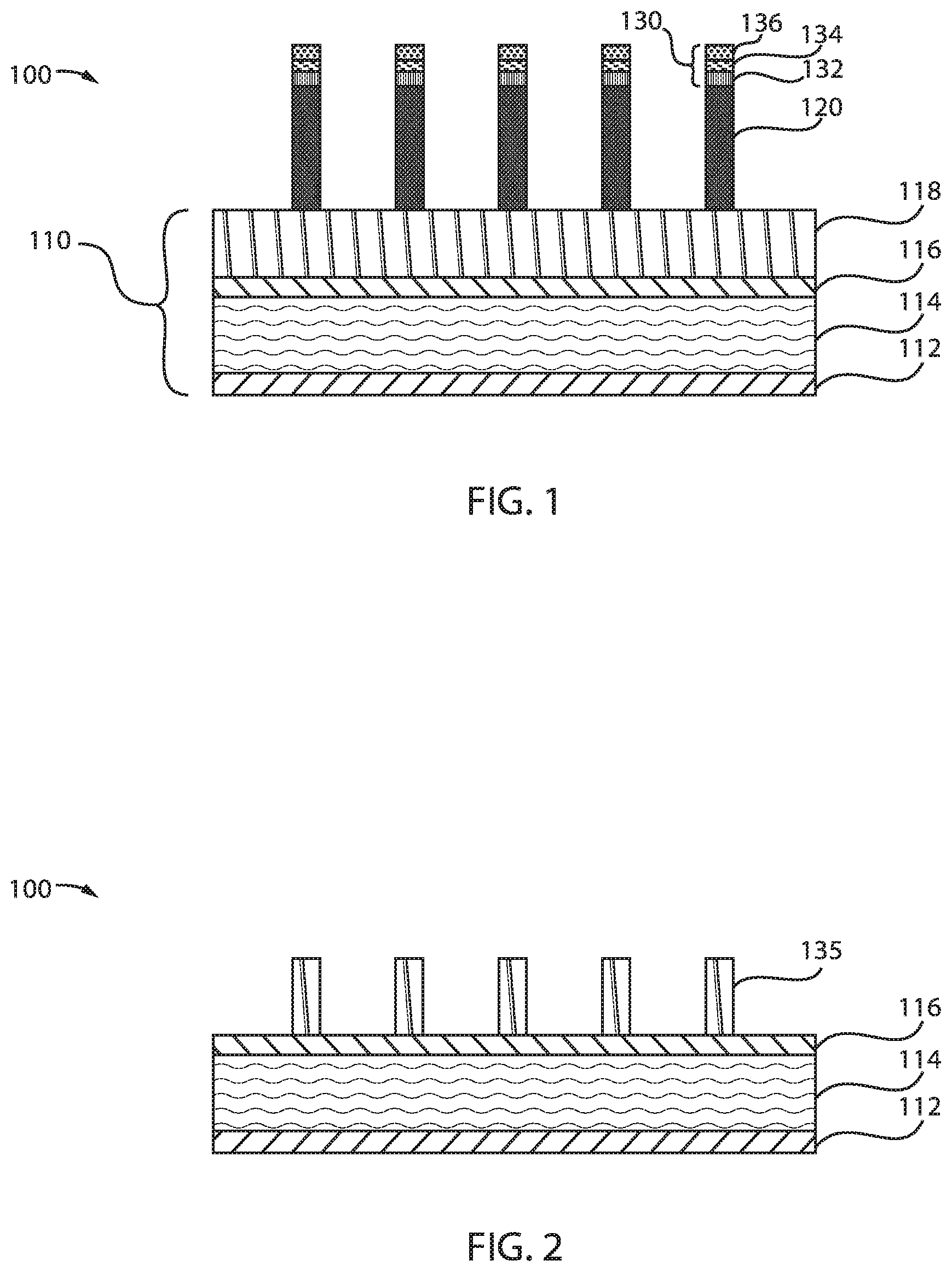
[0008] FIG. 1 is a cross-sectional view of mandrel lithography performed during the fabrication of the semiconductor device, in accordance with an embodiment of the present invention;
[0009] FIG. 2 is a cross-sectional view of a mandrel etch and removal of a planarization layer performed during the fabrication of the semiconductor device, in accordance with an embodiment of the present invention;
[0010] FIG. 3 is a cross-sectional view of a spacer layer formed during the fabrication of the semiconductor device, in accordance with an embodiment of the present invention
[0011] FIG. 4 is a cross-sectional view of an etch back of the spacer layer and formation of a hard mask material during the fabrication of the semiconductor device, in accordance with an embodiment of the present invention;
[0012] FIG. 5 is a cross-sectional view of a photo-sensitive material formed during the fabrication of the semiconductor device, in accordance with an embodiment of the present invention;
[0013] FIG. 6 is a cross-sectional view of a single exposure scheme performed to expose cut patterns during the fabrication of the semiconductor device, in accordance with an embodiment of the present invention;
[0014] FIG. 7 is a cross-sectional view of the removal of mandrels and non-mandrels during the fabrication of the semiconductor device, in accordance with an embodiment of the present invention;
[0015] FIG. 8 is a cross-sectional view of further processing performed during the fabrication of the semiconductor device, in accordance with an embodiment of the present invention;
[0016] FIG. 9 is a cross-sectional view of lithography exposure for at least one mandrel cut pattern of a double exposure scheme performed during the fabrication of the semiconductor device, in accordance with another embodiment of the present invention;
[0017] FIG. 10 is a cross-sectional view of lithography exposure for of at least one non-mandrel cut pattern of a double exposure scheme performed during the fabrication of the semiconductor device, in accordance with another embodiment of the present invention;
[0018] FIG. 11 is a cross-sectional view of the removal of the remaining photo-sensitive material after the cut patterns are exposed during the fabrication of the semiconductor device, in accordance with another embodiment of the present invention;
[0019] FIG. 12 is a cross-sectional view of a memorization layer formed during the fabrication of the semiconductor device, in accordance with yet another embodiment of the present invention;
[0020] FIG. 13 is a cross-sectional view of lithography to create at least one mandrel cut pattern region, and the removal of a portion of the memorization layer corresponding to the at least one mandrel cut pattern region during the fabrication of the semiconductor device, in accordance with yet another embodiment of the present invention;
[0021] FIG. 14 is a cross-sectional view of lithography to create at least one non-mandrel cut pattern region, and the removal of a portion of the memorization layer corresponding to the at least one non-mandrel cut region during the fabrication of the semiconductor device, in accordance with yet another embodiment of the present invention;
[0022] FIG. 15 is a cross-sectional view of cut patterns formed during the fabrication of the semiconductor device, in accordance with yet another embodiment of the present invention; and
[0023] FIG. 16 is a cross-sectional view of the removal of the remaining memorization layer, and the removal of mandrels and non-mandrels during the fabrication of the semiconductor device, in accordance with yet another embodiment of the present invention.
DETAILED DESCRIPTION
[0024] However, obstacles associated with multi-patterning include complicated multiple cut patterning. For example, different patterning schemes can be needed for mandrel cut pattern(s) and non-mandrel cut pattern(s). To address at least some of the obstacles associated with multi-patterning, the embodiments described herein provide for the fabrication of semiconductor devices that integrate a multi-patterning scheme (e.g., SADP) with planarized cut patterning structure and process. The embodiments described herein can employ a gap fill material (e.g., hard mask material) having etch properties similar to the mandrel by backfilling the non-mandrel region after spacer etch back during the multi-patterning process. Thus, a planarized (e.g., flat) surface can be achieved for the proceeding cut patterning steps. In accordance with one illustrative embodiment, the cut patterning can be enabled as a single exposure (e.g., single extreme ultraviolet (EUV) lithography exposure). In an another illustrative embodiment, the cut patterning can be enabled as multiple exposures (e.g., multiple EUV exposures). The embodiments described herein can enable a flat surface for cut patterning in a multi-patterning scheme (e.g., SADP), such that multiple cut patterns can share the same multi-patterning scheme. Furthermore, uniform cut size can be achieved, and scalability of multi-patterning integration beyond the 7 nm regime can be enabled.
[0025] It is to be understood that aspects of the present invention will be described in terms of a given illustrative architecture; however, other architectures, structures, substrate materials and process features and steps can be varied within the scope of aspects of the present invention.
[0026] It will also be understood that when an element such as a layer, region or substrate is referred to as being "on" or "over" another element, it can be directly on the other element or intervening elements can also be present. In contrast, when an element is referred to as being "directly on" or "directly over" another element, there are no intervening elements present. It will also be understood that when an element is referred to as being "connected" or "coupled" to another element, it can be directly connected or coupled to the other element or intervening elements can be present. In contrast, when an element is referred to as being "directly connected" or "directly coupled" to another element, there are no intervening elements present.
[0027] The present embodiments can include a design for an integrated circuit chip, which can be created in a graphical computer programming language, and stored in a computer storage medium (such as a disk, tape, physical hard drive, or virtual hard drive such as in a storage access network). If the designer does not fabricate chips or the photolithographic masks used to fabricate chips, the designer can transmit the resulting design by physical means (e.g., by providing a copy of the storage medium storing the design) or electronically (e.g., through the Internet) to such entities, directly or indirectly. The stored design is then converted into the appropriate format (e.g., GDSII) for the fabrication of photolithographic masks, which typically include multiple copies of the chip design in question that are to be formed on a wafer. The photolithographic masks are utilized to define areas of the wafer (and/or the layers thereon) to be etched or otherwise processed.
[0028] Methods as described herein can be used in the fabrication of integrated circuit chips. The resulting integrated circuit chips can be distributed by the fabricator in raw wafer form (that is, as a single wafer that has multiple unpackaged chips), as a bare die, or in a packaged form. In the latter case, the chip is mounted in a single chip package (such as a plastic carrier, with leads that are affixed to a motherboard or other higher level carrier) or in a multichip package (such as a ceramic carrier that has either or both surface interconnections or buried interconnections). In any case, the chip is then integrated with other chips, discrete circuit elements, and/or other signal processing devices as part of either (a) an intermediate product, such as a motherboard, or (b) an end product. The end product can be any product that includes integrated circuit chips, ranging from toys and other low-end applications to advanced computer products having a display, a keyboard or other input device, and a central processor.
[0029] It should also be understood that material compounds will be described in terms of listed elements, e.g., SiGe. These compounds include different proportions of the elements within the compound, e.g., SiGe includes Si.sub.xGe.sub.1-x where x is less than or equal to 1, etc. In addition, other elements can be included in the compound and still function in accordance with the present principles. The compounds with additional elements will be referred to herein as alloys.
[0030] Reference in the specification to "one embodiment" or "an embodiment", as well as other variations thereof, means that a particular feature, structure, characteristic, and so forth described in connection with the embodiment is included in at least one embodiment. Thus, the appearances of the phrase "in one embodiment" or "in an embodiment", as well any other variations, appearing in various places throughout the specification are not necessarily all referring to the same embodiment.
[0031] It is to be appreciated that the use of any of the following "/", "and/or", and "at least one of", for example, in the cases of "A/B", "A and/or B" and "at least one of A and B", is intended to encompass the selection of the first listed option (A) only, or the selection of the second listed option (B) only, or the selection of both options (A and B). As a further example, in the cases of "A, B, and/or C" and "at least one of A, B, and C", such phrasing is intended to encompass the selection of the first listed option (A) only, or the selection of the second listed option (B) only, or the selection of the third listed option (C) only, or the selection of the first and the second listed options (A and B) only, or the selection of the first and third listed options (A and C) only, or the selection of the second and third listed options (B and C) only, or the selection of all three options (A and B and C). This can be extended, as readily apparent by one of ordinary skill in this and related arts, for as many items listed.
[0032] The terminology used herein is for the purpose of describing particular embodiments only and is not intended to be limiting of example embodiments. As used herein, the singular forms "a," "an" and "the" are intended to include the plural forms as well, unless the context clearly indicates otherwise. It will be further understood that the terms "comprises," "comprising," "includes" and/or "including," when used herein, specify the presence of stated features, integers, steps, operations, elements and/or components, but do not preclude the presence or addition of one or more other features, integers, steps, operations, elements, components and/or groups thereof.
[0033] Spatially relative terms, such as "beneath," "below," "lower," "above," "upper," and the like, can be used herein for ease of description to describe one element's or feature's relationship to another element(s) or feature(s) as illustrated in the FIGS. It will be understood that the spatially relative terms are intended to encompass different orientations of the device in use or operation in addition to the orientation depicted in the FIGS. For example, if the device in the FIGS. is turned over, elements described as "below" or "beneath" other elements or features would then be oriented "above" the other elements or features. Thus, the term "below" can encompass both an orientation of above and below. The device can be otherwise oriented (rotated 90 degrees or at other orientations), and the spatially relative descriptors used herein can be interpreted accordingly. In addition, it will also be understood that when a layer is referred to as being "between" two layers, it can be the only layer between the two layers, or one or more intervening layers can also be present.
[0034] It will be understood that, although the terms first, second, etc. can be used herein to describe various elements, these elements should not be limited by these terms. These terms are only used to distinguish one element from another element. Thus, a first element discussed below could be termed a second element without departing from the scope of the present concept.
[0035] Referring now to the drawings in which like numerals represent the same or similar elements, FIGS. 1-16 depict respective steps of process flows for fabricating semiconductor devices integrating respective multi-patterning schemes.
[0036] In the illustrative embodiment depicted in FIGS. 1-8, the multi-patterning scheme includes a single exposure scheme to expose at least one mandrel cut pattern and at least one non-mandrel cut pattern.
[0037] In the illustrative embodiment depicted in FIGS. 9-11, the multi-patterning scheme includes a double exposure scheme to expose the mandrel and non-mandrel cut patterns.
[0038] In the illustrative embodiment depicted in FIGS. 12-16, the multi-patterning scheme includes a litho-etch-litho-etch scheme to expose the mandrel and non-mandrel cut patterns.
[0039] Referring now to FIG. 1, a cross-sectional view is provided showing an exemplary semiconductor device 100 having a base structure 110. The base structure 110 includes a metal cap layer 112, a dielectric layer 114, a hard mask layer 116 and a dielectric layer 118. The metal cap layer 112 can include any suitable material in accordance with the embodiments described herein. The dielectric layer 114 is an inter-metal dielectric (IMD) layer, and can include any suitable material in accordance with the embodiments described herein. The hard mask layer 116 can include, e.g., titanium nitride (TiN), although any suitable material can be used in accordance with the embodiments described herein. As will be described in further detail below, mandrels will be formed from the dielectric layer 118. As such, any suitable material can be used to form the dielectric layer 118 in accordance with the embodiments described herein (e.g., an oxide material). For example, the dielectric layer 118 can include an oxide formed by a chemical vapor deposition (CVD) process (e.g., plasma-enhanced CVD (PECVD). In one embodiment, the dielectric layer 118 includes a PECVD tetraethyl orthosilicate (TEOS) oxide.
[0040] As further shown, mandrel lithography is performed, which includes forming planarization layers 120 on the dielectric layer 118. In one embodiment, the planarization layers 120 include organic planarization layers (OPLs). OPLs can be formed from a photo-sensitive organic polymer including a light-sensitive material that, when exposed to radiation (e.g., electromagnetic radiation), is chemically altered for removal using a solvent. Examples of photo-sensitive organic polymers for use as OPLs include, but are not limited to, polyacrylate resin, epoxy resin, phenol resin, polyamide resin, polyimide resin, unsaturated polyester resin, polyphenylenether resin, polyphenylenesulfide resin, or benzocyclobutene (BCB). However, any suitable material can be used in accordance with the embodiments described herein.
[0041] The materials of the planarization layers 120 are selected to be compatible with a resist stack 130 formed on respective ones of the planarization layers 120. The resist stack 130 can each include a hard mask layer 132, an anti-reflective coating (ARC) layer 134 and a resist layer 136.
[0042] The hard mask layer 132 can include a dielectric hard mask material. Examples of dielectric hard mask materials include, e.g., silicon nitrides, silicon oxides, silicon oxynitrides, silicon carbides, silicon carbonitrides, etc. Spin-on dielectrics may also be utilized as a hard mask material include, e.g., silsequioxanes, siloxanes, and boron phosphate silicate glass (BPSG). However, any suitable material can be used in accordance with the embodiments described herein.
[0043] As shown, the ARC layer 134 is a bottom ARC (BARC) layer since it is formed underneath the resist layer 136. The ARC layer 134 includes a material having light absorbing compounds, and uses destructive interference at the interfaces of the ARC layer 134 and the photoresist layer 136. The material of the ARC layer 134 is chosen to have a refractive index suitable for use in accordance with the embodiments described herein. For example, the ARC layer 134 can include any suitable organic and/or inorganic ARC materials.
[0044] The resist layer 136 can include any suitable resist material in accordance with the embodiments described herein.
[0045] Referring to FIG. 2, mandrels 135 are created from the dielectric layer 118, and the photoresist stacks 130 and the planarization layers 120 are removed. Any suitable processes can be used in accordance with the embodiments described herein. For example, a combination of etch processes and/or chemical stripping processes can be used.
[0046] Referring to FIG. 3, a spacer layer 140 is formed using any suitable process in accordance with the embodiments described herein. The spacer layer 140 can include, e.g., silicon nitride (SiN), although any suitable material can be used in accordance with the embodiments described herein.
[0047] Referring to FIG. 4, an etch back is performed to expose gaps between the mandrels 135, referred to herein as "non-mandrel regions," a hard mask material is formed within the non-mandrel regions, and an etch back is performed to create "non-mandrels" 145 in the non-mandrel regions from the hard mask material, using any suitable processes in accordance with the embodiments described herein. The hard mask material of the non-mandrels 145 includes a material that has an etch property substantially similar to that of the material of the mandrels 135 (e.g., the material of the dielectric layer 118). For example, the hard mask material of the non-mandrels 145 can include a spin-on-glass (SOG) material. In one embodiment, the SOG material can include a silicone-based polymer (e.g., a polydimethylsiloxane (PDMS)-based polymer). In another embodiment, the hard mask material can include a spin-on-carbon (SOC) material. Accordingly, mandrels 135 and non-mandrels 145 include materials having substantially similar etch properties.
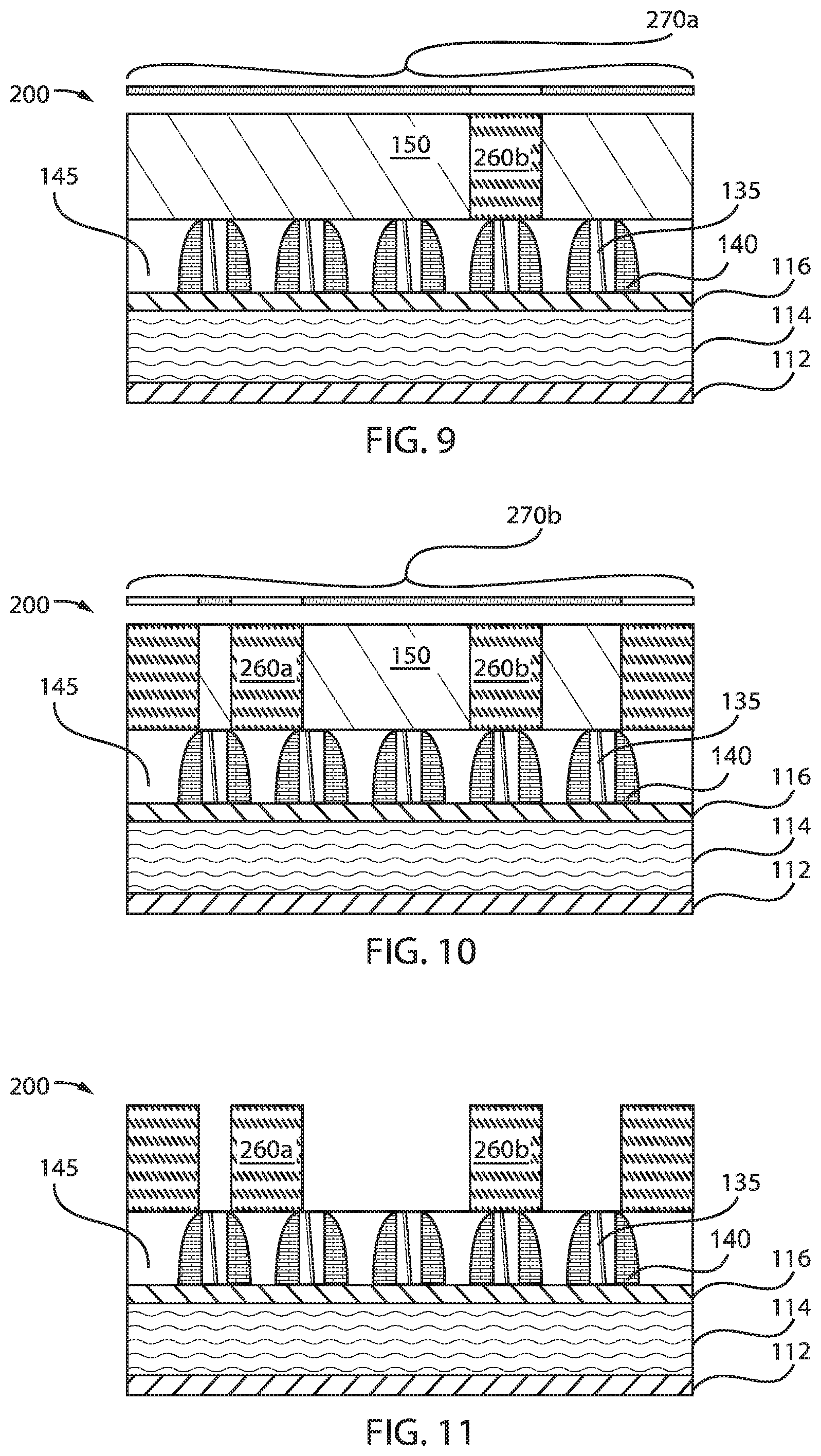
[0048] Referring to FIG. 5, photo-sensitive material 150 is formed using any suitable material in accordance with the embodiments described herein. The photo-sensitive material 150 is formed for implementation in a self-aligned block (SAB) lithography scheme to create both mandrel and non-mandrel cut patterns.
[0049] Referring to FIG. 6, at least one non-mandrel cut pattern 160a and at least one mandrel cut pattern 160b can be simultaneously created over at least one of the non-mandrels 145 and at least one of the mandrels 135 by applying a single exposure scheme (e.g., single EUV exposure) to the photo-sensitive material 150. As shown in FIG. 10, three non-mandrel cut patterns 160a and one mandrel cut pattern 160b are created. However, such an arrangement should not be considered limiting. Thus, a single SAB lithography scheme can be enabled for both the non-mandrel and mandrel cut patterns 160a and 16b for, e.g., a 7 nm node.
[0050] As will be described in further detail below with reference to FIGS. 10-12, the non-mandrel and mandrel cut patterns can, in an alternative embodiment, be created by applying a double exposure scheme to the photo-sensitive material. Thus, a double SAB lithography scheme can be enabled for both the non-mandrel and mandrel cut patterns for, e.g., beyond a 7 nm node.
[0051] Referring to FIG. 7, those of the mandrels 135 and the non-mandrels 145 that are not covered by the cut patterns 160a and 160b are removed or pulled out (e.g., by etching).
[0052] Referring to FIG. 8, one or more etch processes are performed to remove the exposed portions of the hard mask layer 116, and the portions of the dielectric layer 114 exposed after the removal of the exposed portions of the hard mask layer 116. Although not explicitly shown in FIG. 14, portions of the mandrels 135 and the non-mandrels 145 can also be removed during the removal of the dielectric layer 114. Any suitable processes can be used to remove the cut patterns, remove the portions of the hard mask layer 116, and remove the portions of the dielectric layer 114 in accordance with the embodiments described herein.
[0053] As mentioned above, the mandrel and non-mandrel cut patterns can be created using a double exposure scheme (e.g., double EUV exposure), as will now be described with reference to FIGS. 9-11. It is be assumed that semiconductor device 200 described in FIGS. 9-11 has been processed in accordance with FIG. 5.
[0054] Referring to FIG. 9, a lithography exposure is performed to create at least one mandrel cut pattern 260b using a mask 270a. As shown in FIG. 9, one mandrel cut pattern 260b is created. However, such an arrangement should not be considered limiting.
[0055] Referring to FIG. 10, a lithography exposure is performed to create at least one non-mandrel cut pattern 260a. As shown in FIG. 10, three non-mandrel cut patterns 260a are created. However, such an arrangement should not be considered limiting.
[0056] Referring to FIG. 11, the remaining photo-sensitive material 150 is removed using any suitable process in accordance with the embodiments described herein.
[0057] Further downstream processing, including the processing described above in FIGS. 7 and 8, can be performed on the device 200.
[0058] A multi-patterning scheme including a litho-etch-litho-etch scheme to expose the mandrel and non-mandrel cut patterns will now be described with reference to FIGS. 12-16. It is assumed that that semiconductor device 300 described in FIGS. 12-16 has been processed in accordance with FIG. 4.
[0059] Referring to FIG. 12, a memorization layer 310 is formed using any suitable process in accordance with the embodiments described herein. The memorization layer 310 can include, e.g., a titanium oxide (TiO.sub.x), although any suitable material can be used in accordance with the embodiments described herein.
[0060] Referring to FIG. 13, lithography is performed to expose at least one mandrel cut pattern region 325b within a mask 320a using any suitable process in accordance with the embodiments described herein. As shown in FIG. 13, one mandrel cut pattern region 325b is created. However, such an arrangement should not be considered limiting. Then, an etch process is performed to remove the portion of the memorization layer 310 corresponding to the at least one mandrel cut pattern region 325b. Any suitable process can be used to remove the portion of the memorization layer 310 in accordance with the embodiments described herein.
[0061] Referring to FIG. 14, lithography is performed to expose at least one non-mandrel cut pattern region 325a within a mask 320b, which fills the mandrel cut pattern region 325b. As shown in FIG. 21, three non-mandrel cut patterns 260a are created. However, such an arrangement should not be considered limiting. Then, an etch process is performed to remove the portion of the memorization layer 310 corresponding to the at least one non-mandrel cut pattern region 325a. Any suitable process can be used to remove the portion of the memorization layer 310 in accordance with the embodiments described herein.
[0062] Referring to FIG. 15, at least one non-mandrel cut pattern 330a is formed in the at least one non-mandrel cut pattern region 325a and at least one mandrel cut pattern 330b is formed in the at least one mandrel cut pattern region 325b. The cut patterns 330a and 330b can be formed by employing backfill and etch back processes. The cut patterns 330a and 330b can include, e.g., silicon nitride (SiN), although any suitable material can be used in accordance with the embodiments described herein.
[0063] Referring to FIG. 16, the remaining portion of the memorization layer 310 is removed, and those of the mandrels 135 and the non-mandrels 145 that are not covered by the cut patterns 160a and 160b are removed or pulled out (e.g., by etching). Any suitable processes can be used to remove the remaining portion of the memorization layer 310 and those of the mandrels 135 and non-mandrels 145 that are not covered by the cut patterns, in accordance with the embodiments described herein.
[0064] Further downstream processing, including the processing described above in FIG. 8, can be performed on the device 300.
[0065] Having described preferred embodiments of a semiconductor device and a method of fabricating a semiconductor device (which are intended to be illustrative and not limiting), it is noted that modifications and variations can be made by persons skilled in the art in light of the above teachings. It is therefore to be understood that changes may be made in the particular embodiments disclosed which are within the scope of the invention as outlined by the appended claims. Having thus described aspects of the invention, with the details and particularity required by the patent laws, what is claimed and desired protected by Letters Patent is set forth in the appended claims.
* * * * *
D00000
D00001
D00002
D00003
D00004
D00005
D00006
D00007
XML
uspto.report is an independent third-party trademark research tool that is not affiliated, endorsed, or sponsored by the United States Patent and Trademark Office (USPTO) or any other governmental organization. The information provided by uspto.report is based on publicly available data at the time of writing and is intended for informational purposes only.
While we strive to provide accurate and up-to-date information, we do not guarantee the accuracy, completeness, reliability, or suitability of the information displayed on this site. The use of this site is at your own risk. Any reliance you place on such information is therefore strictly at your own risk.
All official trademark data, including owner information, should be verified by visiting the official USPTO website at www.uspto.gov. This site is not intended to replace professional legal advice and should not be used as a substitute for consulting with a legal professional who is knowledgeable about trademark law.