Deposition of organic films
Tois , et al. February 16, 2
U.S. patent number 10,923,361 [Application Number 16/659,012] was granted by the patent office on 2021-02-16 for deposition of organic films. This patent grant is currently assigned to ASM IP Holding B.V.. The grantee listed for this patent is ASM IP Holding B.V.. Invention is credited to Suvi P. Haukka, Krzysztof Kachel, Delphine Longrie, Jan Willem Maes, Viljami J. Pore, Varun Sharma, Hidemi Suemori, Eva E. Tois.

View All Diagrams
| United States Patent | 10,923,361 |
| Tois , et al. | February 16, 2021 |
Deposition of organic films
Abstract
Processes are provided herein for deposition of organic films. Organic films can be deposited, including selective deposition on one surface of a substrate relative to a second surface of the substrate. For example, polymer films may be selectively deposited on a first metallic surface relative to a second dielectric surface. Selectivity, as measured by relative thicknesses on the different layers, of above about 50% or even about 90% is achieved. The selectively deposited organic film may be subjected to an etch process to render the process completely selective. Processes are also provided for particular organic film materials, independent of selectivity. Masking applications employing selective organic films are provided. Post-deposition modification of the organic films, such as metallic infiltration and/or carbon removal, is also disclosed.
| Inventors: | Tois; Eva E. (Espoo, FI), Suemori; Hidemi (Helsinki, FI), Pore; Viljami J. (Helsinki, FI), Haukka; Suvi P. (Helsinki, FI), Sharma; Varun (Helsinki, FI), Maes; Jan Willem (Wilrijk, BE), Longrie; Delphine (Ghent, BE), Kachel; Krzysztof (Leuven, BE) | ||||||||||
|---|---|---|---|---|---|---|---|---|---|---|---|
| Applicant: |
|
||||||||||
| Assignee: | ASM IP Holding B.V. (Almere,
NL) |
||||||||||
| Family ID: | 1000005367356 | ||||||||||
| Appl. No.: | 16/659,012 | ||||||||||
| Filed: | October 21, 2019 |
Prior Publication Data
| Document Identifier | Publication Date | |
|---|---|---|
| US 20200051829 A1 | Feb 13, 2020 | |
Related U.S. Patent Documents
| Application Number | Filing Date | Patent Number | Issue Date | ||
|---|---|---|---|---|---|
| 15486124 | Apr 12, 2017 | 10453701 | |||
| 15170769 | Jul 6, 2019 | 10373820 | |||
| Current U.S. Class: | 1/1 |
| Current CPC Class: | C23C 16/56 (20130101); C23C 16/04 (20130101); H01L 21/02178 (20130101); H01L 21/0337 (20130101); H01L 21/32 (20130101); H01L 21/76834 (20130101); C23C 16/45553 (20130101); H01L 21/02186 (20130101); H01L 21/0228 (20130101); H01L 21/31138 (20130101); H01L 21/02118 (20130101); H01L 21/32139 (20130101); H01L 21/31144 (20130101) |
| Current International Class: | H01L 21/311 (20060101); H01L 21/768 (20060101); C23C 16/455 (20060101); C23C 16/04 (20060101); H01L 21/32 (20060101); H01L 21/3213 (20060101); H01L 21/033 (20060101); H01L 21/02 (20060101); C23C 16/56 (20060101) |
References Cited [Referenced By]
U.S. Patent Documents
| 4804640 | February 1989 | Kaganowicz |
| 4863879 | September 1989 | Kwok |
| 4948755 | August 1990 | Mo |
| 5288697 | February 1994 | Schrepp et al. |
| 5447887 | September 1995 | Filipiak et al. |
| 5604153 | February 1997 | Tsubouchi et al. |
| 5633036 | May 1997 | Seebauer et al. |
| 5869135 | February 1999 | Vaeth et al. |
| 5925494 | July 1999 | Horn |
| 6046108 | April 2000 | Liu et al. |
| 6482740 | November 2002 | Soininen et al. |
| 6586330 | July 2003 | Ludviksson et al. |
| 6679951 | January 2004 | Soininen et al. |
| 6759325 | July 2004 | Raaijmakers et al. |
| 6811448 | November 2004 | Paton et al. |
| 6844258 | January 2005 | Fair et al. |
| 6878628 | April 2005 | Sophie et al. |
| 6887795 | May 2005 | Soininen et al. |
| 6921712 | July 2005 | Soininen et al. |
| 6958174 | October 2005 | Klaus et al. |
| 7067407 | June 2006 | Kostamo et al. |
| 7084060 | August 2006 | Furukawa et al. |
| 7118779 | October 2006 | Verghese et al. |
| 7220669 | May 2007 | Hujanen et al. |
| 7241677 | July 2007 | Soininen et al. |
| 7323411 | January 2008 | Blosse |
| 7405143 | July 2008 | Leinikka et al. |
| 7425350 | September 2008 | Todd |
| 7476618 | January 2009 | Kilpela et al. |
| 7494927 | February 2009 | Kostamo et al. |
| 7595271 | September 2009 | White |
| 7754621 | July 2010 | Putkonen |
| 7790631 | September 2010 | Sharma et al. |
| 7799135 | September 2010 | Verghese et al. |
| 7910177 | March 2011 | Li |
| 7914847 | March 2011 | Verghese et al. |
| 7927942 | April 2011 | Raaijmakers |
| 7955979 | June 2011 | Kostamo et al. |
| 7964505 | June 2011 | Khandelwal et al. |
| 8293597 | October 2012 | Raaijmakers |
| 8293658 | October 2012 | Shero et al. |
| 8425739 | April 2013 | Wieting |
| 8536058 | September 2013 | Kostamo et al. |
| 8778815 | July 2014 | Yamaguchi et al. |
| 8890264 | November 2014 | Dewey et al. |
| 8956971 | February 2015 | Haukka et al. |
| 8962482 | February 2015 | Albertson et al. |
| 8980418 | March 2015 | Darling et al. |
| 8993404 | March 2015 | Korbrinsky et al. |
| 9067958 | June 2015 | Romero |
| 9112003 | August 2015 | Haukka et al. |
| 9129897 | September 2015 | Pore et al. |
| 9136110 | September 2015 | Rathsack |
| 9159558 | October 2015 | Cheng et al. |
| 9236292 | January 2016 | Romero et al. |
| 9257303 | February 2016 | Haukka et al. |
| 9349687 | May 2016 | Gates et al. |
| 9490145 | November 2016 | Niskanen et al. |
| 9502289 | November 2016 | Haukka et al. |
| 9679808 | June 2017 | Haukka et al. |
| 9803277 | October 2017 | Longrie et al. |
| 9895715 | February 2018 | Haukka et al. |
| 9911595 | March 2018 | Smith et al. |
| 10014212 | July 2018 | Chen et al. |
| 10041166 | August 2018 | Longrie et al. |
| 10204782 | February 2019 | Maes et al. |
| 10343186 | July 2019 | Pore et al. |
| 10373820 | August 2019 | Tois et al. |
| 10428421 | October 2019 | Haukka et al. |
| 10453701 | October 2019 | Tois |
| 10546741 | January 2020 | Murakami et al. |
| 10695794 | June 2020 | Pore et al. |
| 10854460 | December 2020 | Tois et al. |
| 2001/0019803 | September 2001 | Mirkanimi |
| 2001/0025205 | September 2001 | Chern et al. |
| 2002/0027261 | March 2002 | Blesser et al. |
| 2002/0047144 | April 2002 | Nguyen et al. |
| 2002/0068458 | June 2002 | Chiang et al. |
| 2002/0090777 | July 2002 | Forbes et al. |
| 2002/0107316 | August 2002 | Bice et al. |
| 2003/0027431 | February 2003 | Sneh et al. |
| 2003/0066487 | April 2003 | Suzuki |
| 2003/0143839 | July 2003 | Raaijmakers et al. |
| 2003/0181035 | September 2003 | Yoon et al. |
| 2003/0192090 | October 2003 | Meilland |
| 2003/0193090 | October 2003 | Otani et al. |
| 2004/0092073 | May 2004 | Cabral |
| 2004/0219746 | November 2004 | Vaartstra et al. |
| 2005/0012975 | January 2005 | George et al. |
| 2005/0136604 | June 2005 | Al-Bayati et al. |
| 2005/0160575 | July 2005 | Gambino et al. |
| 2005/0223989 | October 2005 | Lee et al. |
| 2006/0019493 | January 2006 | Li |
| 2006/0047132 | March 2006 | Shenai-Khatkhate et al. |
| 2006/0121271 | June 2006 | Frey et al. |
| 2006/0141155 | June 2006 | Gordon et al. |
| 2006/0156979 | July 2006 | Thakur et al. |
| 2006/0176559 | August 2006 | Takatoshi et al. |
| 2006/0199399 | September 2006 | Muscat |
| 2006/0226409 | October 2006 | Burr et al. |
| 2006/0292845 | December 2006 | Chiang et al. |
| 2007/0014919 | January 2007 | Hamalainen et al. |
| 2007/0026654 | February 2007 | Huotari et al. |
| 2007/0063317 | March 2007 | Kim et al. |
| 2007/0099422 | May 2007 | Wijekoon et al. |
| 2007/0241390 | October 2007 | Tanaka et al. |
| 2007/0292604 | December 2007 | Dordi et al. |
| 2008/0066680 | March 2008 | Sherman |
| 2008/0072819 | March 2008 | Rahtu |
| 2008/0124932 | May 2008 | Tateishi et al. |
| 2008/0179741 | July 2008 | Streck et al. |
| 2008/0241575 | October 2008 | Lavoie et al. |
| 2008/0282970 | November 2008 | Heys et al. |
| 2009/0035949 | February 2009 | Niinisto et al. |
| 2009/0071505 | March 2009 | Miya et al. |
| 2009/0081385 | March 2009 | Heys et al. |
| 2009/0203222 | August 2009 | Dussarrat et al. |
| 2009/0269507 | October 2009 | Yu et al. |
| 2009/0274887 | November 2009 | Millward et al. |
| 2009/0275163 | November 2009 | Lacey et al. |
| 2009/0311879 | December 2009 | Blasco et al. |
| 2010/0015756 | January 2010 | Weidman et al. |
| 2010/0147396 | June 2010 | Yamagishi et al. |
| 2010/0178468 | July 2010 | Jiang et al. |
| 2010/0248473 | September 2010 | Ishizaka et al. |
| 2010/0270626 | October 2010 | Raisanen |
| 2010/0297474 | November 2010 | Dameron |
| 2011/0039420 | February 2011 | Nakao et al. |
| 2011/0053800 | March 2011 | Jung et al. |
| 2011/0120542 | May 2011 | Levy |
| 2011/0124192 | May 2011 | Ganguli et al. |
| 2011/0146568 | June 2011 | Haukka et al. |
| 2011/0221061 | September 2011 | Prakash |
| 2011/0311726 | December 2011 | Liu et al. |
| 2012/0032311 | February 2012 | Gates |
| 2012/0046421 | February 2012 | Darling et al. |
| 2012/0052681 | March 2012 | Marsh |
| 2012/0088369 | April 2012 | Weidman et al. |
| 2012/0189868 | July 2012 | Borovik et al. |
| 2012/0219824 | August 2012 | Prolier et al. |
| 2012/0241411 | September 2012 | Darling et al. |
| 2012/0264291 | October 2012 | Ganguli et al. |
| 2012/0269970 | October 2012 | Ido et al. |
| 2013/0005133 | January 2013 | Lee et al. |
| 2013/0078793 | March 2013 | Sun et al. |
| 2013/0089983 | April 2013 | Sugita et al. |
| 2013/0095664 | April 2013 | Matero et al. |
| 2013/0115768 | May 2013 | Pore et al. |
| 2013/0146881 | June 2013 | Yamazaki et al. |
| 2013/0189837 | July 2013 | Haukka et al. |
| 2013/0196502 | August 2013 | Haukka et al. |
| 2013/0203267 | August 2013 | Pomarede et al. |
| 2013/0280919 | October 2013 | Yuasa et al. |
| 2013/0284094 | October 2013 | Pavol et al. |
| 2013/0309457 | November 2013 | Rathsack et al. |
| 2013/0316080 | November 2013 | Yamaguchi et al. |
| 2013/0323930 | December 2013 | Chattopadhyay et al. |
| 2014/0001572 | January 2014 | Bohr et al. |
| 2014/0024200 | January 2014 | Kato et al. |
| 2014/0091308 | April 2014 | Dasgupta et al. |
| 2014/0120738 | May 2014 | Jung et al. |
| 2014/0152383 | June 2014 | Nikonov et al. |
| 2014/0190409 | July 2014 | Matsumoto et al. |
| 2014/0193598 | July 2014 | Traser et al. |
| 2014/0205766 | July 2014 | Lyon et al. |
| 2014/0209022 | July 2014 | Inoue et al. |
| 2014/0227461 | August 2014 | Darwish et al. |
| 2014/0273290 | September 2014 | Somervell |
| 2014/0273514 | September 2014 | Somervell et al. |
| 2014/0273523 | September 2014 | Rathsack |
| 2014/0273527 | September 2014 | Niskanen et al. |
| 2015/0004806 | January 2015 | Ndiege et al. |
| 2015/0011032 | January 2015 | Kunimatsu et al. |
| 2015/0011093 | January 2015 | Singh et al. |
| 2015/0037972 | February 2015 | Danek et al. |
| 2015/0064931 | March 2015 | Kumagai et al. |
| 2015/0083415 | March 2015 | Monroe et al. |
| 2015/0087158 | March 2015 | Sugita et al. |
| 2015/0093890 | April 2015 | Blackwell et al. |
| 2015/0097292 | April 2015 | He et al. |
| 2015/0118863 | April 2015 | Rathod et al. |
| 2015/0162214 | June 2015 | Thompson et al. |
| 2015/0170961 | June 2015 | Romero et al. |
| 2015/0179798 | June 2015 | Clendenning et al. |
| 2015/0217330 | August 2015 | Haukka et al. |
| 2015/0240121 | August 2015 | Sugita et al. |
| 2015/0299848 | October 2015 | Haukka et al. |
| 2015/0371866 | December 2015 | Chen et al. |
| 2015/0376211 | December 2015 | Girard et al. |
| 2016/0075884 | March 2016 | Chen |
| 2016/0079524 | March 2016 | Do et al. |
| 2016/0086850 | March 2016 | Romero et al. |
| 2016/0186004 | June 2016 | Hustad et al. |
| 2016/0190060 | June 2016 | Bristol et al. |
| 2016/0222504 | August 2016 | Haukka et al. |
| 2016/0247695 | August 2016 | Niskanen et al. |
| 2016/0276208 | September 2016 | Haukka et al. |
| 2016/0284568 | September 2016 | Morris et al. |
| 2016/0293398 | October 2016 | Danek et al. |
| 2016/0346838 | December 2016 | Fujita et al. |
| 2016/0365280 | December 2016 | Brink et al. |
| 2017/0037513 | February 2017 | Haukka et al. |
| 2017/0040164 | February 2017 | Wang et al. |
| 2017/0058401 | March 2017 | Blackwell et al. |
| 2017/0069527 | March 2017 | Haukka et al. |
| 2017/0100742 | April 2017 | Pore et al. |
| 2017/0100743 | April 2017 | Pore et al. |
| 2017/0107413 | April 2017 | Wang et al. |
| 2017/0154806 | June 2017 | Wang et al. |
| 2017/0298503 | October 2017 | Maes et al. |
| 2017/0301542 | October 2017 | Maes et al. |
| 2017/0323776 | November 2017 | Farm et al. |
| 2017/0332179 | November 2017 | Bright et al. |
| 2017/0352533 | December 2017 | Tois et al. |
| 2017/0352550 | December 2017 | Tois et al. |
| 2018/0222933 | August 2018 | Romero |
| 2018/0233350 | August 2018 | Tois et al. |
| 2019/0017170 | January 2019 | Sharma et al. |
| 2019/0057858 | February 2019 | Hausmann et al. |
| 2019/0074441 | March 2019 | Kikuchi et al. |
| 2019/0155159 | May 2019 | Knaepen et al. |
| 2019/0283077 | September 2019 | Pore et al. |
| 2019/0333761 | October 2019 | Tois et al. |
| 0469456 | Feb 1992 | EP | |||
| 0880168 | Nov 1998 | EP | |||
| 1340269 | Feb 2009 | EP | |||
| H08-222569 | Aug 1996 | JP | |||
| 4333900 | Sep 2009 | JP | |||
| 2009-231783 | Oct 2009 | JP | |||
| 2011/0187583 | Sep 2011 | JP | |||
| 2011-222779 | Nov 2011 | JP | |||
| 2013-229622 | Nov 2013 | JP | |||
| 2013-247287 | Dec 2013 | JP | |||
| 2014/093331 | May 2014 | JP | |||
| 2015-99881 | May 2015 | JP | |||
| 1020010010172 | Feb 2001 | KR | |||
| 20030027392 | Apr 2003 | KR | |||
| 1020040056026 | Jun 2004 | KR | |||
| 10-0869326 | Nov 2008 | KR | |||
| 10-2012-0120902 | Nov 2012 | KR | |||
| 175767 | Aug 2003 | TW | |||
| 2005/39321 | Dec 2005 | TW | |||
| 2010/05827 | Feb 2010 | TW | |||
| 2014/39365 | Oct 2014 | TW | |||
| WO 2002/045167 | Jun 2002 | WO | |||
| WO 2011/156705 | Dec 2011 | WO | |||
| WO 2013/161772 | Oct 2013 | WO | |||
| WO 2014/156782 | Oct 2014 | WO | |||
| WO 2014/209390 | Dec 2014 | WO | |||
| WO 15/047345 | Apr 2015 | WO | |||
| WO 2015/047345 | Apr 2015 | WO | |||
| WO 2015/094305 | Jun 2015 | WO | |||
| WO 2015/147843 | Oct 2015 | WO | |||
| WO 2015/147858 | Oct 2015 | WO | |||
| WO 17/184357 | Oct 2017 | WO | |||
| WO 2017/184357 | Oct 2017 | WO | |||
| WO 2017/184358 | Oct 2017 | WO | |||
Other References
|
Office Action dated Apr. 8, 2020 in Taiwan Application No. 105132286. cited by applicant . "Tungsten and Tungsten Silicide Chemical Vapor Deposition", TimeDomain CVD, Inc., retrieved from link: http://www.timedomaincvd.com/CVD_Fundamentals/films/W_WSi.html, Last modified Jul. 11, 2008. cited by applicant . Au et al., "Selective Chemical Vapor Deposition of Manganese Self/Aligned Capping Layer for Cu Interconnections in Microelectronics", Journal of the Electrochemical Society, vol. 157, No. 6, 2010, pp. D341/D345. cited by applicant . Bernal-Ramos, et al., "Atomic Layer Deposition of Cobalt Silicide Thin Films Studied by in Situ Infrared Spectroscopy", Chem. Mater. 2015, 27, pp. 4943-4949. cited by applicant . Bouteville et al., "Selective R.T.L.P.C.V.D. Of Tungsten by Silane Reduction on Patterned PPQ/Si Wafers" Journal De Physique IV, Colloque C2, suppl. au Journal de Physique II, vol. 1, Sep. 1991, pp. C2/857/C2/864. cited by applicant . Burton, et al., "Atomic Layer Deposition of MgO Using Bis(ethylcyclopentadienyl)magnesium and H20". J. Phys. Chem. C, 2009, 113, 1939/1946. cited by applicant . Burton, et al., "Si02 Atomic Layer Deposition Using Tris(dimethylamino)silane and Hydrogen Peroxide Studied by in Situ Transmission FTIR Spectroscopy". J. Phys. Chem. C, 2009, 113, 8249/8257. cited by applicant . Carlsson, J., "Precursor Design for Chemical Vapour Deposition", Acta Chemica Scandinavica, vol. 45, 1991, pp. 864/869. cited by applicant . Chang et al, "Influences of damage and contamination from reactive ion etching on selective tungsten deposition in a low/pressure chemical/vapor/deposition reactor", J. Appl. Phys., vol. 80, No. 5, Sep. 1, 1996, pp. 3056/3061. cited by applicant . Chen et al., Highly Stable Monolayer Resists for Atomic Layer Deposition on Germanium and Silicon, Chem. Matter, vol. 18, No. 16, pp. 3733/3741, 2006. cited by applicant . Coclite, et al.; 25th Anniversary Article: CVD Polymers: A New Paradigm for Surface Modification and Device Fabrication; Advanced Materials; Oct. 2013; 25; pp. 5392/5423. cited by applicant . Elam et al., "Kinetics of the WF6 and Si2H6 surface reactions during tungsten atomic layer deposition", Surface Science, vol. 479, 2001, pp. 121/135. cited by applicant . Elam et al., "Nucleation and growth during tungsten atomic layer deposition on SiO2 surfaces", Thin Solid Films, vol. 386, 2001 pp. 41/52. cited by applicant . Ellinger et al., "Selective Area Spatial Atomic Layer Deposition of ZnO, Al2O3, and Aluminum-Doped ZnO Using Poly(vinyl pyrrolidone)", Chem Mater. 2014, 26:1514-1522. cited by applicant . Fabreguette et al., Quartz crystal microbalance study of tungsten atomic layer deposition using WF6 and Si2H6, Thin Solid Films, vol. 488, 2005, pp. 103/110. cited by applicant . Farm et al. Selective/Area Atomic Layer Deposition Using Poly( methyl methacrylate) Films as Mask Layers, J. Phys. Chem. C, 2008, 112, pp. 15791/15795. (Year: 2008). cited by applicant . Farr, Isaac Vincent; Synthesis and Characterization of Novel Polyimide Gas Separation Membrane Material Systems, Chapter 2; Virginia Tech Chemistry PhD Dissertation; URN # etd/080999/123034; Jul. 26, 1999. cited by applicant . File History of U.S. Appl. No. 13/702,992, filed Mar. 26, 2013. cited by applicant . File History of U.S. Appl. No. 13/708,863, filed Dec. 7, 2012. cited by applicant . File History of U.S. Appl. No. 15/177,195, filed Jun. 8, 2016. cited by applicant . George, Steven M.; Atomic Layer Deposition: An Overview; Chem. Rev. 2010, 110, pp. 111-131; Feb. 12, 2009. cited by applicant . Ghosal et al., Controlling Atomic Layer Deposition of Ti02 in Aerogels through Surface Functionalization, Chem. Matter, vol. 21, pp. 1989/1992, 2009. cited by applicant . Grubbs et al., "Nucleation and growth during the atomic layer deposition of W on Al2O3 and Al2O3 on W", Thin Solid Films, vol. 467, 2004, pp. 16/27. cited by applicant . Hymes et al., "Surface cleaning of copper by thermal and plasma treatment in reducing and inert ambients", J. Vac. Sci. Technol. B, vol. 16, No. 3, May/Jun. 1998, pp. 1107/1109. cited by applicant . International Search Report and Written Opinion dated Feb. 17, 2012 in Application No. PCT/US2011/039970, filed Jun. 10, 2011 in 12 pages. cited by applicant . International Search Report and Written Opinion dated Jun. 16, 2017 in Application No. PCT/US2017/026518, filed Apr. 7, 2017 in 13 pages. cited by applicant . International Search Report and Written Opinion dated Jun. 22, 2017 in Application No. PCT/US2017/026519, filed Apr. 7, 2017 in 12 pages. cited by applicant . International Search Report and Written Opinion dated Jun. 20, 2017 in Application No. PCT/US2017/026515, filed Apr. 7, 2017 in 11 pages. cited by applicant . King, Dielectric Barrier, Etch Stop, and Metal Capping Materials for State of the Art and beyond Metal Interconnects, ECS Journal of Solid State Science and Technology, vol. 4, Issue 1, pp. N3029/N3047, 2015. cited by applicant . Klaus et al., "Atomic layer deposition of tungsten using sequential surface chemistry with a sacrificial stripping reaction", Thin Solid Films, vol. 360, 2000, pp. 145/153. cited by applicant . Klaus et al., "Atomically controlled growth of tungsten and tungsten nitride using sequential surface reactions", Applied Surface Science 162/163, 2000, pp. 479/491. cited by applicant . Lee et al., Area-Selective Atomic Layor Deposition Using Self/Assembled Monolayer and Scanning Probe Lithography, Journal of the Electrochemical Society, vol. 156, Issue 9, pp. G125/G128, 2009. cited by applicant . Lei et al., "Real/time observation and opitimization of tungsten atomic layer deposition process cycle", J. Vac. Sci. Technol. B, vol. 24, No. 2, Mar./Apr. 2006, pp. 780/789. cited by applicant . Lemonds, A.M., "Atomic Layer Deposition and Properties of Refractory Transition Metal/Based Copper/Diffusion Barriers for ULSI Interconnect", The University of Texas at Austin, 2003, Dissertation in 216 pages. cited by applicant . Leusink et al., "Growth kinetics and inhibition of growth of chemical vapor deposited thin tungsten films on silicon from tungsten hexafluoride", J. Appl. Phys., vol. 72, No. 2, Jul. 15, 1992, pp. 490/498. cited by applicant . Liang, et al., "Growth of Ge Nanofilms Using Electrochemical Atomic Layer Deposition, with a "Bait and Switch" Surface/Limited Reaction". JACS, 2011, 133:8199-8204. cited by applicant . Lohokare et al., "Reactions of Disilane on Cu(111): Direct Observation of Competitive Dissociation, Disproportionation, and Thin Film Growth Processes", Langmuir 1995, vol. 11, pp. 3902-3912. cited by applicant . Low et al., Selective deposition of CVD iron on silicon dioxide and tungsten, Microelectronic Engineering 83, pp. 2229-2233, 2006. cited by applicant . Mackus et al., Influence of Oxygen Exposure on the Nucleation of Platinum Atomic Layer Deposition: Consequences for Film Growth, Nanopatterning, and Nanoparticle Synthesis, Chem. Matter, vol. 25, pp. 1905-1911, 2013. cited by applicant . Mackus et al., Local deposition of high/purity Pt nanostructures by combining electron beam induced deposition and atomic layer deposition, J Appl Phys., vol. 107, pp. 116102/1-116102/3, 2010. cited by applicant . Mackus, et al., The use of atomic layer deposition in advanced nanopatterning; Nanoscale (2014) 6:10941-10960. cited by applicant . Maluf et al., "Selective tungsten filling of sub/0.25.mu.m trenches for the fabrication of scaled contacts and x/ray masks", J. Vac. Sci. Technol. B, vol. 8, No. 3, May/Jun. 1990, pp. 568-569. cited by applicant . Norrman, et al.; 6 Studies of Spin/Coated Polymer Films; Annu. Rep. Prog. Chem.; Sect. C; 2005; 101; pp. 174-201. cited by applicant . Notice of Allowance dated Apr. 5, 2017 in U.S. Appl. No. 15/177,195. cited by applicant . Office Action dated Aug. 29, 2014 in U.S. Appl. No. 13/702,992. cited by applicant . Office Action dated Nov. 7, 2014 in U.S. Appl. No. 13/708,863. cited by applicant . Overhage et al., Selective Atomic Layer Deposition (SALD) of Titanium Dioxide on Silicon and Copper Patterned Substrates, Journal of Undergraduate Research 4, 29, Mar. 2011 in 4 pages. cited by applicant . Parulekar et al., Atomic Layer Deposition of Zirconium Oxide on Copper Patterned Silicon Substrate, Journal of Undergraduate Research, vol. 7, pp. 15-17, 2014. cited by applicant . Parulekar et al., Selective atomic layer deposition of zirconium oxide on copper patterned silicon substrate, pp. 1-6, 2013. cited by applicant . Prasittichai et al., "Area Selective Molecular Layer Deposition of Polyurea Film", Applied Materials & Interfaces, 2013, 5:13391-13396. cited by applicant . Proslier et al., "Atomic Layer Deposition and Superconducting Properties of NbSi Films", The Journal of Physical Chemistry C, 2011, vol. 115, No. 50, pp. 1-26. cited by applicant . Putkonen, et al.; Atomic Layer Deposition of Polyimide Thin Films; Journal of Materials Chemistry; 2007, 17, pp. 664-669. cited by applicant . Ratta, Varun; Crystallization, Morphology, Thermal Stability and Adhesive Properties of Novel High Performance Semicrystalline Polyimides, Chapter 1; Virginia Tech Chemistry PhD Dissertation; URN # etd/051799/162256; Apr. 26, 1999 in 29 pages. cited by applicant . Roberts et al., "Selective Mn deposition on Cu lines", poster presentation, 12th International Conference on Atomic Layer Deposition, Jun. 19, 2012, Dresden, Germany; in 1 page. cited by applicant . Sapp, et al.; Thermo/Mechanical and Electrical Characterization of Through/Silicon Vias with a Vapor Deposited Polyimide Dielectric Liner; IEEE; 2012. cited by applicant . Schmei er, Decomposition of formic acid, Chemnitz University of Technology, pp. 1/13, Aug. 31, 2011. cited by applicant . Schmei er, Reduction of Copper Oxide by Formic Acid an ab/initio study, Chemnitz University of Technology, pp. 1/42, Sep. 2011. cited by applicant . Schuisky, et al., Atomic Layer Deposition of Thin Films Using O2 as Oxygen Source; Langmuir (2001) 17:5508-5512. cited by applicant . Selvaraj et al., Selective atomic layer deposition of zirconia on copper patterned silicon substrates using ethanol as oxygen source as well as copper reductant, Journal of Vacuum Science & Technology A, vol. 32, No. 1, pp. 010601/1-010601/4, Jan. 2014. cited by applicant . Senesky et al., "Aluminum nitride as a masking material for the plasma etching of silicon carbide structures," 2010, IEEE, pp. 352/355. cited by applicant . Sundberg, et al.; Organic and Inorganic-Organic Thin Film Structures by Molecular Layer Deposition: A Review; Beilstein J. Nanotechnol; 2014, 5, pp. 1104-1136. cited by applicant . Suntola, "Handbook of Crystal Growth. vol. 3., Thin Films and Epitaxy, Part B: Growth mechanisms and Dynamics", Amsterdam: North Holland, Elsevier Science Publishers (1994), Chapter 14, pp. 601-662. cited by applicant . Toirov, et al.; Thermal Cyclodehydration of Polyamic Acid Initiated by UV/Irradiation; Iranian Polymer Journal; vol. 5, No. 1; pp. 16/22; 1996; Iran. cited by applicant . Vallat et al., Selective deposition of Ta205 by adding plasma etching super/cycles in plasma enhanced atomic layer deposition steps, Journal of Vacuum Science & Technology A, vol. 35, No. 1, pp. 01B104/1-01B104/7, Jan. 2017. cited by applicant . Vervuurt et al. "Area/selective atomic layer deposition of platinum using photosensitive polymide," (2016) Nanotechnology 27.40 (2016): 405302. cited by applicant . Yu et al., "Gas/surface reactions in the chemical vapor deposition of tungsten using WF6/SiH4 mixtures", J. Vac. Sci. Technol. A, vol. 7, No. 3, May/Jun. 1989, pp. 625-629. cited by applicant . Zhou, et al.; Fabrication of Organic Interfacial Layers by Molecular Layer Deposition: Present Status and Future Opportunities; Journal of Vacuum Science & Technology; A 31 (4), 040801/1 to 040801/18; 2013 in 18 pages. cited by applicant . Aaltonen et al., "Atomic Layer Deposition of Iridium Thin Films," Journal of Electrochemical Society, 151(8):G489-G492, 2004. cited by applicant . Benzotriazole, Wikipedia via https://en.wikipedia.org/wiki/Benzotriazole; pp. 1-5, no date available. cited by applicant . Formic Acid, Wikipedia via https://en.wikipedia.org/wiki/Formic_acid; pp. 1-5, no date available. cited by applicant . George, S.M. et al., "Surface chemistry for molecular layer deposition of organic and hybrid organic-inorganic polymers," Accounts of Chemical Research, Apr. 2009, vol. 42, No. 4, pp. 498-508. cited by applicant . Hashemi et al., "A New Resist for Area Selective Atomic and Molecular Layer Deposition on Metal-Dielectric Patterns", J. Phys. Chem. C 2014, 118, pp. 10957-10962. cited by applicant . Hashemi et al., "Selective Deposition of Dieletrics: Limits and Advantages of Alkanethiol Blocking Agents on Metal-Dielectric Patterns", ACS Appl. Mater. Interfaces 2016, 8, pp. 33264-33272. cited by applicant . Kukli et al., Properties of hafnium oxide films grown by atomic layer deposition from hafnium tetraiodid and oxygen, J.App. Phys., 92(1), 2002, pp. 5698-5703. cited by applicant . Lecordier et al., "Vapor-deposited octadecanethlol masking layer on copper to enable area selective Hf3N4 atomic layer deposition on dielectrics studied by in situ spectroscopic ellipsometry", J. Vac. Sci. Technol. A36(3), May/Jun. 2018, pp. 031605-1-031605-8. cited by applicant . Ting, et al., "Selective Electroless Metal Deposition for Integrated Circuit Fabrication", J. Electrochem. Soc., vol. 136, No. 2, Feb. 1989, pp. 456-462. cited by applicant. |
Primary Examiner: Nikmanesh; Seahvosh
Attorney, Agent or Firm: Knobbe, Martens, Olson & Bear, LLP
Parent Case Text
CROSS-REFERENCE TO RELATED APPLICATIONS
The present application is a continuation of U.S. application Ser. No. 15/486,124 filed Apr. 12, 2017, entitled "DEPOSITION OF ORGANIC FILMS," now U.S. Pat. No. 10,453,701, which is a continuation-in-part of U.S. application Ser. No. 15/170,769, filed Jun. 1, 2016, entitled "DEPOSITION OF ORGANIC FILMS," now U.S. Pat. No. 10,373,820, the disclosures of both of which are hereby incorporated herein by reference in their entireties.
This application is also related to U.S. application Ser. No. 15/070,594, filed Mar. 15, 2016, entitled "VAPOR PHASE DEPOSITION OF ORGANIC FILMS," now U.S. Pat. No. 10,343,186, and to U.S. application Ser. No. 14/879,962, filed Oct. 9, 2015, entitled "VAPOR PHASE DEPOSITION OF ORGANIC FILMS," the disclosures of which are hereby incorporated herein by reference in their entireties.
Claims
What is claimed is:
1. A process for forming an infiltrated film on a substrate, the process comprising: performing a deposition process including contacting the substrate with at least one vapor phase precursor forming an organic film; and subjecting the organic film to an infiltration process to incorporate a metal into the organic film and thereby form the infiltrated film.
2. The process of claim 1, wherein contacting the substrate with at least one vapor phase precursor comprises alternately and sequentially contacting the organic film with a first vapor phase precursor and a second vapor phase precursor.
3. The process of claim 2, wherein the substrate comprises a first surface and a second surface and the deposition process selectively forms the organic film on the first surface relative to the second surface.
4. The process of claim 3, wherein selectively forming the organic film further comprises subjecting the substrate to an etch process, wherein the etch process removes substantially all of any formed organic film from the second surface of the substrate and does not remove all of the formed organic film from the first surface of the substrate.
5. A process for selectively processing the substrate of claim 3, the process comprising: conducting the process of claim 3 to form the infiltrated film selectively on the first surface of the substrate relative to the second surface; and processing an underlying surface of the substrate using the infiltrated film as a mask.
6. The process of claim 5, wherein processing the underlying surface comprises etching a layer below the infiltrated film in order to form a structure, wherein the etching is selective to the material of the layer relative to the infiltrated film.
7. The process of claim 6, wherein the etching comprises a halide based etching process.
8. The process of claim 6, wherein the etching comprises reactive ion etching (RIE) and the structure comprises a substantially vertical sidewall.
9. The process of claim 6, wherein the infiltrated film has a higher etch resistance to the etching the layer below the infiltrated film than the organic film.
10. The process of claim 6, wherein the layer is disposed on an underlying layer and further comprising further etching the underlying layer in order to form the structure.
11. The process of claim 10, wherein further etching comprises selectively etching the underlying layer relative to the infiltrated film.
12. The process of claim 5, wherein the infiltrated film has higher density, conductivity, resistivity, or hardness than the organic film.
13. The process of claim 5, wherein incorporating the metal comprises incorporating an elemental metal, multiple metals, metal alloy, metal oxide, metal nitride, metal carbide and/or combinations thereof.
14. The process of claim 5, wherein the metal comprises a transition metal or post-transition metal.
15. The process of claim 5, wherein the metal comprises aluminum or titanium.
16. The process of claim 5, wherein the infiltration process comprises incorporating aluminum oxide (A1203) and/or titanium dioxide (TiO2) into the selectively formed organic film.
17. The process of claim 5, wherein the first surface is a metallic surface, the second surface is a dielectric surface, and the organic film comprises a polyimide film.
18. The process of claim 5, wherein processing the underlying surface comprises using the infiltrated film as an etch mask in a tone reversal process.
19. The process of claim 5, wherein processing the underlying surface comprises using the infiltrated film as a block mask in a block mask process.
20. The process of claim 1, wherein the infiltration process comprises alternately and sequentially exposing the organic film to a first reactant and a second reactant.
21. The process of claim 20, wherein the first reactant comprises the metal and the second reactant comprises oxygen.
22. The process of claim 20, wherein the first reactant comprises trimethylaluminum (TMA) and the second reactant comprises water (H.sub.2O).
23. The process of claim 20, wherein the first reactant comprises the metal and the second reactant comprises nitrogen.
24. The process of claim 20, wherein the first reactant comprises the metal and the second reactant comprises carbon.
Description
BACKGROUND
Field
The present disclosure relates to deposition of organic thin films, including selective deposition on a first surface of a substrate relative to a second surface. Processes are also provided for particular organic film materials, independent of selectivity.
Description of the Related Art
Organic thin films have valuable optical, thermal, electrical and mechanical properties and are widely used in the electronics, medical engineering, defense, pharmaceutical, and micro- and nanotechnology industries. Polymers in the microelectronics and photonics industries include, among other examples, photon- or electron-curable/degradable polymers for lithographic patterning; and polyimides for packaging, interlayer dielectrics and flexible circuit boards. Norrman et al., Annu. Rep. Prog. Chem., Sect. C, 2005, 101, 174-201.
Polymer thin films can be used, for example, as a starting point in semiconductor applications for amorphous carbon films or layers. Polyimide films are valuable for their thermal stability and resistance to mechanical stress and chemicals. For example, polyimide films can also be used as antireflection layers to improve pattern definition and reduce misalignment in lithography steps, as layers in multiple patterning (e.g., SDDP, SDQP), as insulating materials for interlayer dielectric materials, as the gate dielectric in all-organic thin film transistors, as passivation films in packaging applications, as mask layers in etching processes, etc. Similarly, polyamide and other organic films are valuable for their electrical properties and material properties for numerous applications. Polyamide films may be used, for example, as insulating materials for interlayer dielectric materials in integrated circuit fabrication, and the photosensitivity of polyamide through ultraviolet (UV) curing allows patterning without separate photoresist.
Polymer thin films have traditionally been fabricated through spin-coating techniques. The spin-coating method forms highly functional polymer films by coating a rotating disc with a liquid material and sintering the liquid. However, tailoring of spin-applied films is limited for several reasons. For instance, formation of uniform thin films on a substrate is difficult to control, in part because of the viscosity of the starting liquid, and it can be difficult to fill the gaps of very small features (e.g., trenches or gaps between metal lines) without void generation after curing. Also, spin-coating over high topography relative to the desired thickness of the layer can result in discontinuous and non-conformal deposition. As semiconductor chip sizes continue to shrink, thinner and higher-strength films with more tunable morphology are required.
Recently, vapor phase deposition processes such as chemical vapor deposition (CVD), vapor deposition polymerization (VDP), molecular layer deposition (MLD), and sequential deposition processes such as atomic layer deposition (ALD) and cyclical CVD have been applied to the formation of polymer thin films. In CVD, a film is deposited when reactants react on a substrate surface. Gases of one or more reactants are delivered to one or more substrates in a reaction chamber. In thermal CVD, reactant gases react with one another on a hot substrate to form thin films, with the growth rate typically influenced by the temperature and the amount of reactant supplied. In plasma enhanced CVD, one or more reactants can be activated in a remote plasma generator or in situ. CVD can be performed cyclically with intervening pauses or film treatments. In ALD, deposition is also conducted by cyclical exposure of substrates to reactants, where films are built up through self-saturating reactions between the substrate surface and vapor reactants performed in cycles. The substrate or wafer is exposed to vapor phase reactants, alternatingly and repeatedly, to form a thin film of material on the substrate. In a typical process, one reactant adsorbs in a self-limiting process on the substrate. A different, subsequently pulsed reactant reacts with the adsorbed species of the first reactant to form no more than a single molecular layer of the desired material. Thicker films are produced through repeated growth cycles until the target thickness is achieved. Plasma enhanced variants of ALD, and hybrid ALD/CVD processes (e.g., with some overlap of the substrate exposure to reactant supplies) are also known.
In many applications, for example in forming etches masks, polymer films are formed and subsequently patterned over a substrate. Typically, this patterning is achieved using photolithographic techniques. However, precise placement of the lithographic pattern is required in order to correctly align the patterned polymer film with the underlying substrate features. Often such patterning results in misaligned patterned polymer films. Further, the need for precision placement of the lithographic pattern can introduce complexities into processes where such techniques are used. A need exists for more efficient and reliable techniques for depositing polymer films and for depositing polymer films aligned to features of an underlying substrate. A similar need exists for films containing metal or metallic compounds aligned to features of an underlying substrate.
SUMMARY OF THE INVENTION
In some aspect, processes for selectively depositing an organic film on a substrate comprising a first surface and a second surface are provided. In some embodiments the process may comprise one or more deposition cycles comprising contacting the substrate with a first vapor phase precursor, and contacting the substrate with a second vapor phase precursor, wherein contacting the substrate with the first and second vapor phase precursors forms the organic thin film selectively on the first surface relative to the second surface. In some embodiments processes may further comprise repeating the contacting steps until an organic thin film of a desired thickness has been formed. In some embodiments the first surface may be a metallic surface. In some embodiments the second surface may be a dielectric surface. In some embodiments the organic film may comprise a polyimide film. In some embodiments the substrate may be contacted with the second vapor phase precursor before the substrate is contacted with the first vapor phase precursor. In some embodiments the first vapor phase precursor may comprise a diamine. In some embodiments the substrate is contacted with the first vapor phase precursor comprising a diamine before it is contacted with another, different precursor.
In some embodiments the first vapor phase precursor comprises 1,6-diamnohexane (DAH). In some embodiments the second vapor phase precursor comprises a dianyhydride. In some embodiments the second vapor phase precursor comprises pyromellitic dianhydride (PMDA). In some embodiments the substrate is held at a temperature of greater than about 170.degree. C. during the one or more deposition cycles. In some embodiments the organic film comprises a polyamide film. In some embodiments the first vapor phase precursor comprises a halogen. In some embodiments the first vapor phase precursor comprises adipoyl chloride (AC). In some embodiments the second vapor phase precursor comprises a diamine. In some embodiments the second vapor phase precursor comprises an ethylene diamine. In some embodiments the substrate is held at a temperature of greater than about 80.degree. C. during the one or more deposition cycles. In some embodiments the organic film is deposited on the first surface relative to the second surface with a selectivity of above about 10%. In some embodiments the organic film is deposited on the first surface relative to the second surface with a selectivity of above about 50%. In some embodiments the organic film is deposited on the first surface relative to the second surface with a selectivity of above about 80%. In some embodiments the first surface comprises a metal oxide, elemental metal, or metallic surface. In some embodiments the first surface comprises tungsten. In some embodiments the second surface comprises silicon. In some embodiments the second surface comprises SiO.sub.2. In some embodiments the process is an atomic layer deposition (ALD) type process.
In some embodiments the process may further comprise subjecting the substrate to an etch process, wherein the etch process removes substantially all of any deposited organic film from the second surface of the substrate and does not remove substantially all of the deposited organic film from the first surface of the substrate. In some embodiments the etch process comprises exposing the substrate to hydrogen atoms, hydrogen radicals, hydrogen plasma, or combinations thereof. In some embodiments the etch process comprises exposing the substrate to oxygen atoms, oxygen radicals, oxygen plasma, or combinations thereof. In some embodiments the etch process may comprise exposing the substrate to plasma comprising noble gas species, for example Ar or He species, with or without additional reactive species.
In some aspects processes for selectively depositing an organic film on a substrate comprising a first surface and a second surface are provided. In some embodiments the processes may comprise one or more deposition cycles comprising alternately and sequentially contacting the substrate with a first vapor phase precursor and a second vapor phase precursor, wherein the organic film is selectively formed on the first surface of the substrate relative to the second surface of the substrate. In some embodiments the first surface is a metallic surface. In some embodiments the second surface is a dielectric surface. In some embodiments the organic film is deposited on the first surface relative to the second surface with a selectivity of above about 50%.
In some aspects processes for depositing a polyamide film on a substrate are provided. In some embodiments the processes may comprise one or more deposition cycles comprising contacting the substrate with a first vapor phase precursor comprising 5 or fewer carbon atoms, contacting the substrate with a second vapor phase precursor comprising 3 or fewer carbons, and wherein contacting the substrate with the first and second vapor phase precursors forms a polyamide film of a desired thickness. In some embodiments the process is a vapor deposition process. In some embodiments the process is a molecular layer deposition (MLD) process. In some embodiments the substrate comprises a first surface and a second, different surface. In some embodiments the polyamide film is formed selectively on the first surface of the substrate relative to the second surface of the substrate. In some embodiments the first vapor phase precursor comprises chlorine or dicarboxylic acid. In some embodiments the first vapor phase precursor comprises adipoyl chloride (AC). In some embodiments the second vapor phase precursor comprises an amine. In some embodiments the second vapor phase precursor comprises ethylene diamine (EDA).
In some aspects processes are provided for selectively forming an organic thin film on a substrate comprising a first surface and a second surface. In some embodiments the processes may comprise depositing an organic thin film on the first surface of the substrate and the second surface of the substrate, and exposing the deposited organic thin film to an etchant, wherein exposing the deposited organic thin film to an etchant removes substantially all of the deposited organic thin film from the second surface of the substrate and does not remove substantially all of the deposited organic thin film from the first surface of the substrate. In some embodiments depositing an organic film on the first surface of the substrate and the second surface of the substrate comprises selectively depositing the organic thin film on the first surface of the substrate relative to the second surface of the substrate.
According to some aspects processes for forming an etch mask on a first surface of a substrate comprising the first surface and a second surface are provided. In some embodiments the process may comprise contacting the substrate with a first vapor phase precursor and contacting the substrate with a second vapor phase precursor, wherein contacting the substrate with the first and second vapor phase precursors forms an organic film selectively on the first surface relative to the second surface. The etch mask comprises the organic film formed on the first surface of the substrate.
In some embodiments the contacting steps may comprise a deposition cycle and the process may comprise one or more deposition cycles. In some embodiment the process may further comprise repeating the contacting steps until an etch mask of a desired thickness has been formed. In some embodiments the first surface is a metallic surface. In some embodiments the second surface is a dielectric surface. In some embodiments the organic film comprises a polyimide film. In some embodiments the first vapor phase precursor comprises a diamine. In some embodiments the first vapor phases precursor comprises 1,6-diamnohexane (DAH). In some embodiments the second vapor phase precursor comprises a dianyhydride. In some embodiments the second vapor phase precursor comprises pyromellitic dianhydride (PMDA). In some embodiments the process may further comprise subjecting the substrate to an etch process, wherein the etch process removes substantially all of any formed organic film from the second surface of the substrate and does not remove substantially all of the formed organic film from the first surface of the substrate. In some embodiments the etch mask is used in a tone reversal process. In some embodiments the etch mask comprises a block mask for use in a block mask process.
According to some aspects processes for forming an infiltrated film on a first surface of a substrate comprising the first surface and a second surface are provided. In some embodiments a process comprises performing a selective deposition process comprising contacting the substrate with a first vapor phase precursor and contacting the substrate with a second vapor phase precursor, wherein contacting the substrate with the first and second vapor phase precursors forms an organic thin film selectively on the first surface relative to the second surface. The selectively formed organic film is subjected to an infiltration process to incorporate a metal into the selectively formed organic film and thereby form the infiltrated film.
In some embodiments the contacting steps of the selective deposition process comprise a deposition cycle and the selective deposition process comprises one or more deposition cycles. In some embodiments the metallic material comprises a metal, metal alloy, metal oxide, metal nitride, metal carbide and/or combinations thereof. In some embodiments the infiltration process comprises alternately and sequentially exposing the selectively formed organic film to a first reactant comprising the metal and a second reactant. In some embodiments aluminum oxide (Al.sub.2O.sub.3) is incorporated into the selectively formed organic film. In some embodiments aluminum oxide (Al.sub.2O.sub.3) is incorporated into the selectively formed organic film, the first reactant comprises trimethylaluminum (TMA), and the second reactant comprises H.sub.2O. In some embodiments titanium dioxide (TiO.sub.2) is incorporated into the selectively formed organic film. In some embodiments the process may further comprise subjecting the selectively formed organic film to an ashing process removing carbon from the selectively formed organic film. In some embodiments the ashing process comprises exposing the selectively formed organic film to oxygen atoms, oxygen radicals, oxygen plasma, or combinations thereof. In some embodiments the infiltrated film has an increased resistance to an HF etch relative to the same film that has not been subjected to an infiltration process.
BRIEF DESCRIPTION OF THE DRAWINGS
FIG. 1 is a flow diagram generally illustrating processes for selectively depositing an organic film.
FIG. 2 is a flow diagram generally illustrating atomic layer deposition (ALD) processes for selectively depositing an organic film.
FIG. 3 is a flow diagram generally illustrating processes for selectively depositing an organic film on a first metallic surface of a substrate relative to a second dielectric surface.
FIG. 4 is a flow diagram generally illustrating processes for infiltrating an organic film with inorganic material.
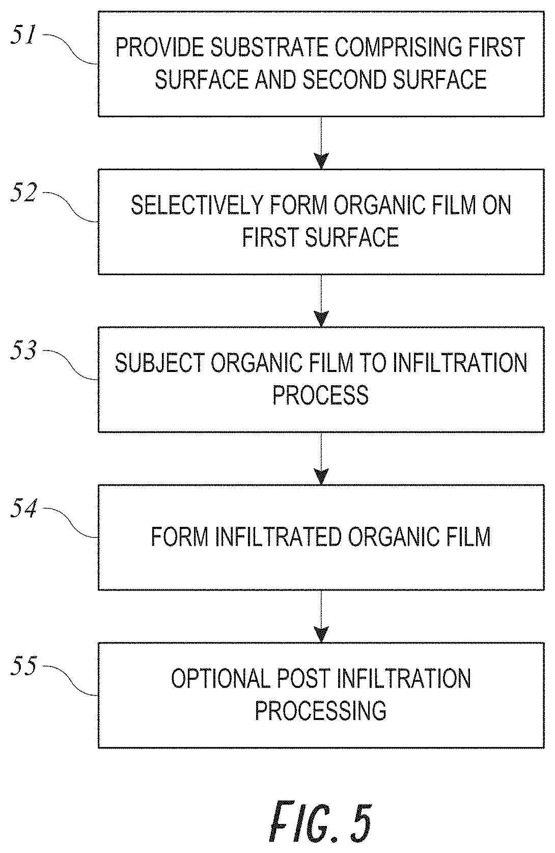
FIG. 5 is a flow diagram generally illustrating processes for infiltrating an organic film with inorganic material including an ashing process to reduce or eliminate carbon from the film.
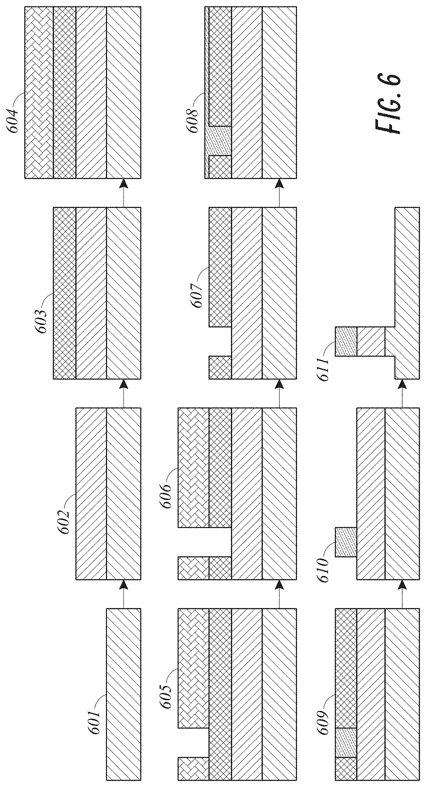
FIG. 6 is a series of schematic cross sections generally illustrating an exemplary tone reversal process for forming a feature on a substrate using an organic film selectively deposited on a first surface of a substrate relative to a second dielectric surface.
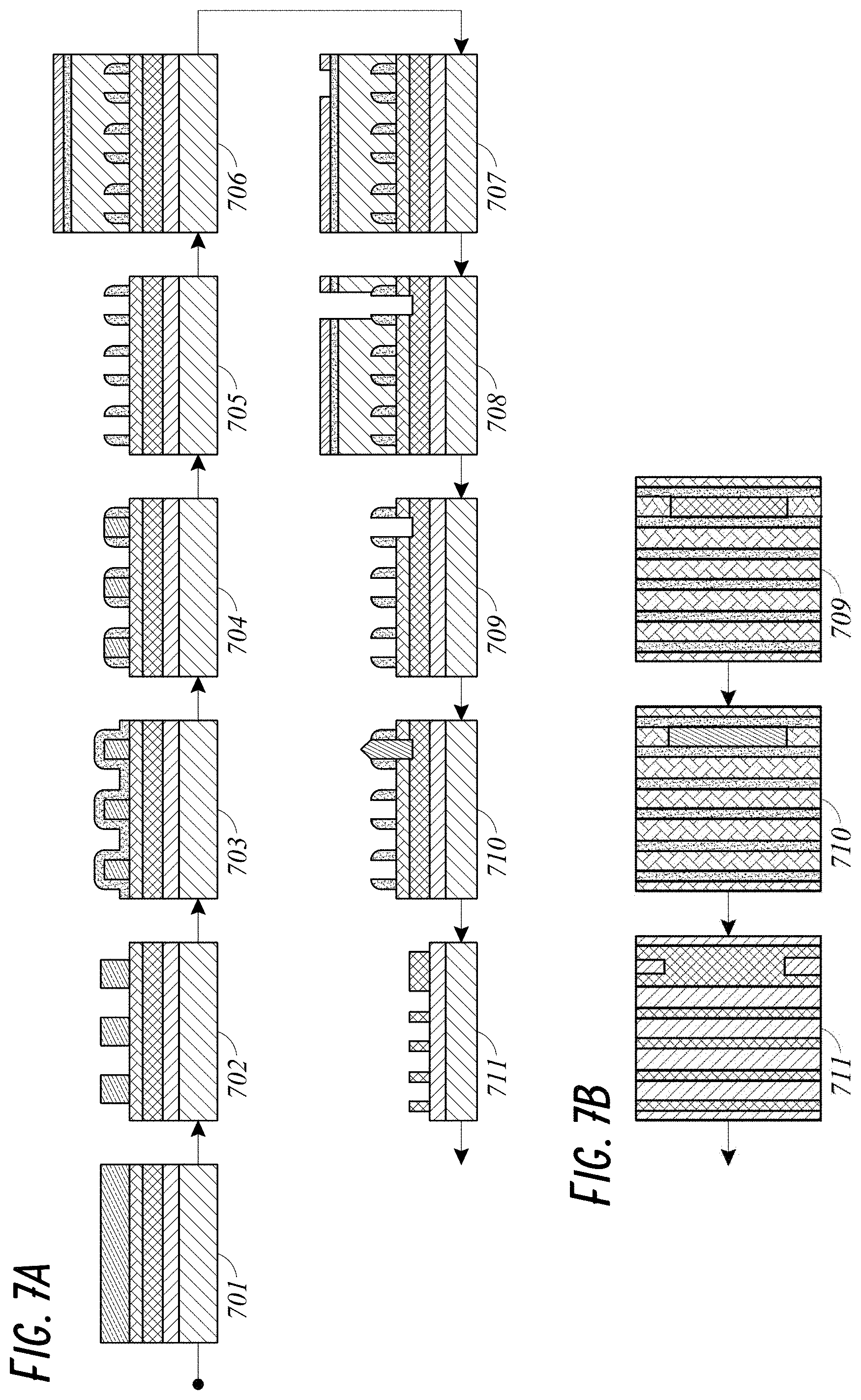
FIG. 7A is a series of schematic cross sections generally illustrating a semiconductor device fabrication process including a block mask formed by selectively depositing an organic film on a first surface of a substrate relative to a second dielectric surface.
FIG. 7B is a series of plan views generally illustrating stages of the semiconductor fabrication process of FIG. 7A, including a block mask formed by selectively depositing an organic film on a first surface of a substrate relative to a second dielectric surface.
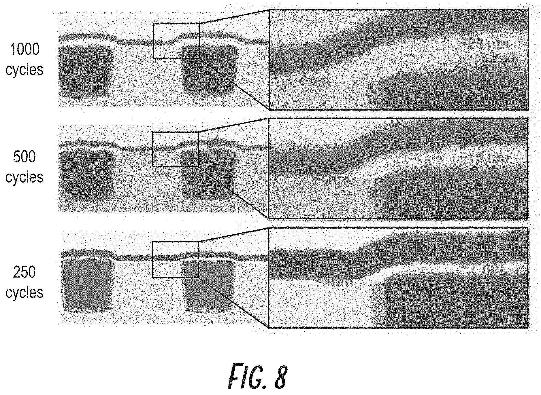
FIG. 8 is a series of cross-sectional scanning transmission electron micrographs showing the thicknesses of selectively deposited polyimide films.
FIG. 9A is a cross-section scanning electron micrograph of a polyamide film deposited on a crystalline silicon substrate having a 1.5 nm native oxide surface.
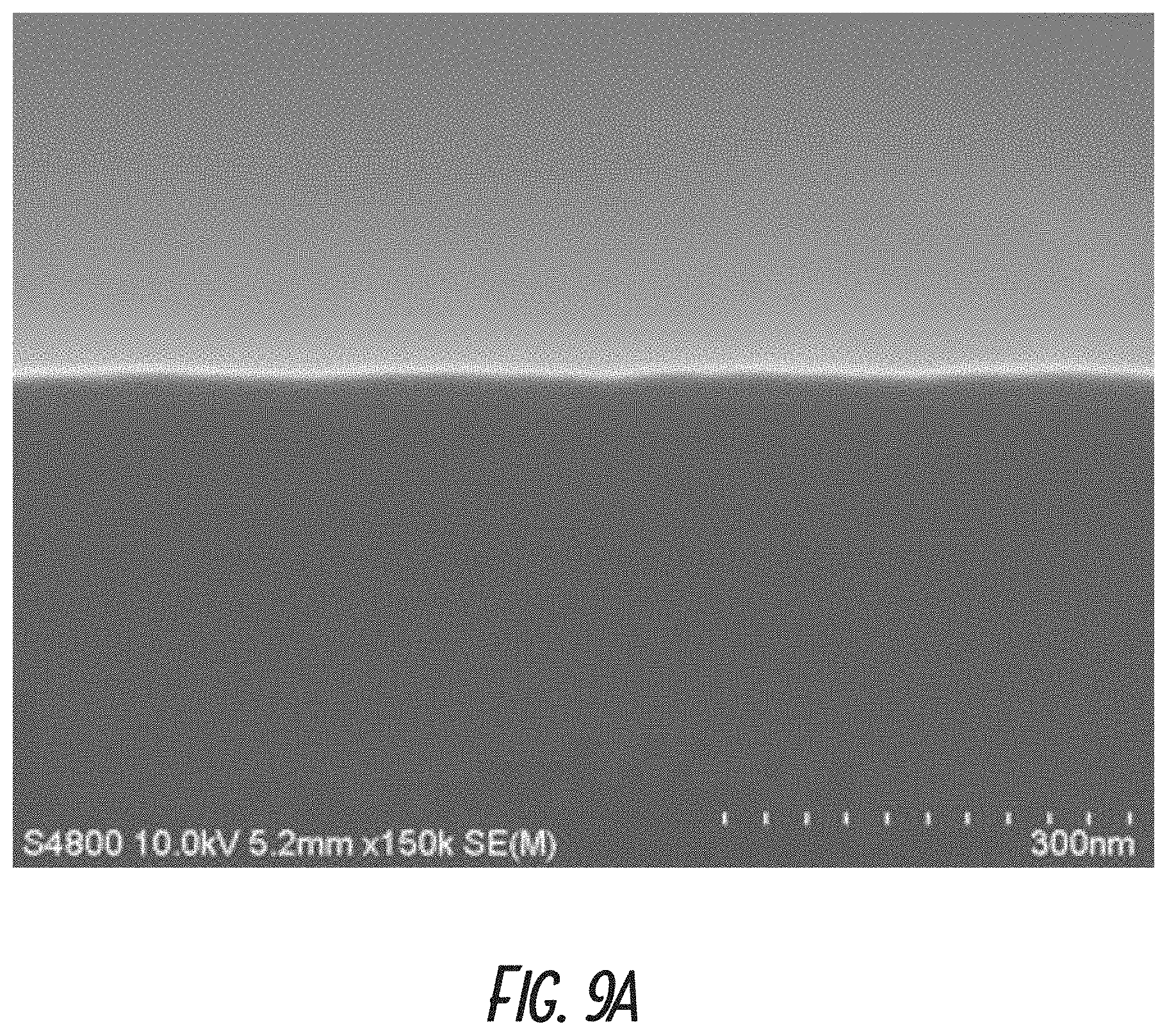
FIG. 9B is a cross-sectional scanning electron micrograph of a polyamide film selectively deposited on the W surfaces of a substrate relative to the oxide surfaces of the same substrate.
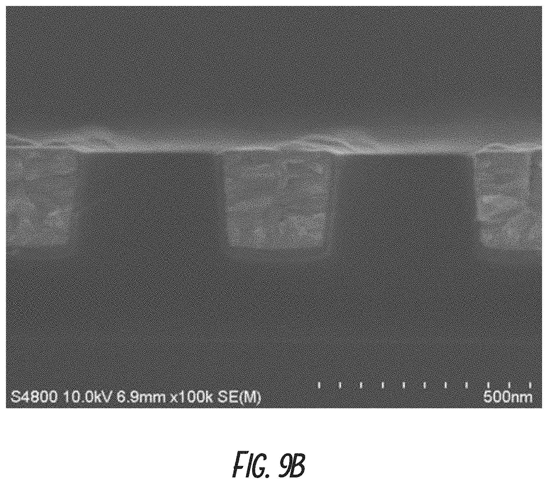
FIG. 10A is a cross-sectional scanning transmission electron micrograph of a polyamide thin film selectively deposited on a W surface of a substrate relative to a silicon oxide surface of the same substrate.
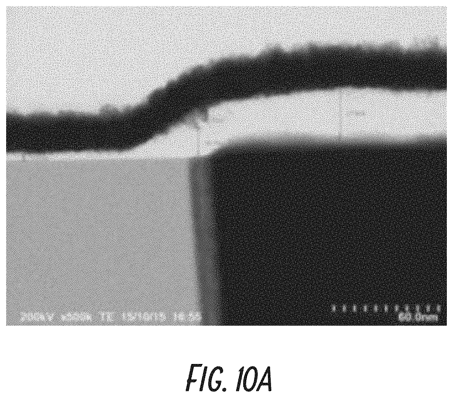
FIG. 10B is a cross-sectional scanning transmission electron micrograph of a polyamide thin film selectively deposited on a W surface of a substrate relative to a silicon oxide surface of the same substrate after being subjected to an etching process.
FIG. 10C is a magnified view of the polyamide thin film on the W surface and the adjacent silicon oxide surface of FIG. 10B.
FIG. 11A is a plot showing growth rate (.ANG./cycle) as a function of ethylenediamine (EDA) precursor contacting time (seconds) for polyamide sample films deposited according to some embodiments.
FIG. 11B is a plot showing growth rate (.ANG./cycle) as a function of adipoyl chloride (AC) precursor contacting time (seconds) for polyamide sample films deposited according to some embodiments.
FIG. 11C is a plot showing growth rate (.ANG./cycle) as a function of precursor removal time (seconds) for polyamide sample films deposited according to some embodiments.
FIG. 11D is a plot showing growth rate (.ANG./cycle) as a function of deposition temperature for polyamide sample films deposited according to some embodiments.
FIG. 12A shows an ellipsometer thickness map for a polyamide film deposited at 71.degree. C. according to some embodiments.
FIG. 12B shows an ellipsometer thickness map for a polyamide film deposited at 50.degree. C. according to some embodiments.
DETAILED DESCRIPTION
According to some aspects of the present disclosure, selective deposition can be used to deposit an organic material on a first surface relative to a second surface. The two surfaces can have different material properties. In some embodiments an organic material is selectively deposited on a first conductive (e.g., metal or metallic) surface of a substrate relative to a second dielectric surface of the substrate. In some embodiments the second surface comprises --OH groups, such as a silicon oxide-based surface. In some embodiments the second surface may additionally comprise --H terminations, such as an HF dipped Si or HF dipped Ge surface. In such embodiments, the surface of interest will be considered to comprise both the --H terminations and the material beneath the --H terminations. In some embodiments an organic material such as a polyamide or polyimide is selectively deposited on a first dielectric surface of a substrate relative to a second, different dielectric surface. In some such embodiments, the dielectrics have different compositions (e.g., silicon, silicon nitride, carbon, silicon oxide, silicon oxynitride, germanium oxide). In other such embodiments, the dielectrics can have the same basic composition (e.g., silicon oxide-based layers) but different material properties due to the manner of formation (e.g., thermal oxides, native oxides, deposited oxides). In some embodiments vapor deposition methods are used. In some embodiments cyclical vapor deposition is used, for example, cyclical CVD or atomic layer deposition (ALD) processes are used. After selective deposition of the organic material is completed, further processing can be carried out to form the desired structures. Advantageously, selectivity can be achieved without passivation/blocking agents on the surface to receive less of the organic layer; and/or without catalytic agents on the surface to receive more of the organic layer.
For embodiments in which one surface comprises a metal whereas the other surface does not, unless otherwise indicated, if a surface is referred to as a metal surface herein, it may be a metal surface or a metallic surface. In some embodiments the metal or metallic surface may comprise metal, metal oxides, and/or mixtures thereof. In some embodiments the metal or metallic surface may comprise surface oxidation. In some embodiments the metal or metallic material of the metal or metallic surface is electrically conductive with or without surface oxidation. In some embodiments metal or a metallic surface comprises one or more transition metals. In some embodiments a metal or metallic surface comprises aluminum. In some embodiments the metal or metallic surface comprises one or more of Al, Cu, Co, Ni, W, Nb, Fe. In some embodiments a metallic surface comprises titanium nitride. In some embodiments the metal or metallic surface comprises one or more noble metals, such as Ru. In some embodiments the metal or metallic surface comprises a conductive metal oxide, nitride, carbide, boride, or combination thereof. For example, the metal or metallic surface may comprise one or more of RuO.sub.x, NbC.sub.x, NbB.sub.x, NiO.sub.x, CoO.sub.x, NbO.sub.x, WNCx, TaN, or TiN.
In some embodiments the metal or metallic surface may comprise Zn, Fe, Mn, or Mo. In some embodiments the metal or metallic surface may be any surface that can accept or coordinate with the first or second precursor utilized in a selective deposition process as described herein.
In some embodiments an organic material is selectively deposited on a metal oxide surface relative to other surfaces. A metal oxide surface may be, for example a WO.sub.x, HfO.sub.x, TiO.sub.x, AlO.sub.x or ZrO.sub.x surface. In some embodiments a metal oxide surface is an oxidized surface of a metallic material. In some embodiments a metal oxide surface is created by oxidizing at least the surface of a metallic material using oxygen compound, such as compounds comprising O.sub.3, H.sub.2O, H.sub.2O.sub.2, O.sub.2, oxygen atoms, plasma or radicals or mixtures thereof. In some embodiments a metal oxide surface is a native oxide formed on a metallic material.
In some embodiments the first surface may comprise a passivated metal surface, for example a passivated Cu surface. That is, in some embodiments the first surface may comprise a metal surface comprising a passivation layer, for example an organic passivation layer such as a benzotriazole (BTA) layer.
In some embodiments an organic material is selectively deposited on a first dielectric surface relative to a second SiO.sub.2 surface. In some embodiments an organic material is selectively deposited on a first dielectric surface relative to a second Si or Ge surface, for example an HF-dipped Si or HF-dipped Ge surface.
In some embodiments an organic material is selectively deposited on a first metal or metallic surface of a substrate relative to a second dielectric surface of the substrate. In some embodiments the organic material that is selectively deposited is a polyamide, polyimide, or other polymeric material. The term dielectric is used in the description herein for the sake of simplicity in distinguishing from the other surface, namely the metal or metallic surface. It will be understood by the skilled artisan that not all non-conducting surfaces are dielectric surfaces. For example, the metal or metallic surface may comprise an oxidized metal surface that is electrically non-conducting or has a very high resistivity. Selective deposition processes taught herein can deposit on such non-conductive metallic surfaces with minimal deposition on adjacent dielectric surfaces.
In some embodiments an organic material is selectively deposited on a first metal oxide surface of a substrate relative to a second SiO.sub.2 surface. In some embodiment the first metal oxide surface may be, for example a WO.sub.x, HfO.sub.x, TiO.sub.x, AlO.sub.x or ZrO.sub.x surface. In some embodiments the organic material is deposited on a first dielectric surface relative to a second SiO.sub.2 surface. In some embodiments the second SiO.sub.2 surface may be, for example, a native oxide, a thermal oxide or a chemical oxide. In some embodiments an organic material is selectively deposited on a first metal oxide surface relative to a second Si or Ge surface, for example an HF-dipped Si or HF-dipped Ge surface.
In some embodiments a substrate is provided comprising a first metal or metallic surface and a second dielectric surface. In some embodiments a substrate is provided that comprises a first metal oxide surface. In some embodiments the second surface may comprise --OH groups. In some embodiments the second surface may be a SiO.sub.2 based surface. In some embodiments the second surface may comprise Si--O bonds. In some embodiments the second surface may comprise a SiO.sub.2 based low-k material. In some embodiments the second surface may comprise more than about 30%, or more than about 50% of SiO.sub.2. In some embodiments the second surface may comprise GeO.sub.2. In some embodiments the second surface may comprise Ge--O bonds. In some embodiments an organic material is selectively deposited on a first metal or metallic surface relative to a second Si or Ge surface, for example an HF-dipped Si or HF-dipped Ge surface.
In certain embodiments the first surface may comprise a silicon dioxide surface and the second dielectric surface may comprise a second, different silicon dioxide surface. For example, in some embodiments the first surface may comprise a naturally or chemically grown silicon dioxide surface. In some embodiments the second surface may comprise a thermally grown silicon dioxide surface. In other embodiments, the first or the second surface may be replaced with a deposited silicon oxide layer. Therefore, in some embodiments organic material may be selectively deposited on a first silicon dioxide surface of a substrate relative to a second silicon dioxide surface that was formed by a different technique and therefore has different material properties.
In some embodiments the substrate may be pretreated or cleaned prior to or at the beginning of the selective deposition process. In some embodiments the substrate may be subjected to a plasma cleaning process at prior to or at the beginning of the selective deposition process. In some embodiments a plasma cleaning process may not include ion bombardment, or may include relatively small amounts of ion bombardment. For example, in some embodiments the substrate surface may be exposed to plasma, radicals, excited species, and/or atomic species prior to or at the beginning of the selective deposition process. In some embodiments the substrate surface may be exposed to hydrogen plasma, radicals, or atomic species prior to or at the beginning of the selective deposition process. In some embodiments a pretreatment or cleaning process may be carried out in the same reaction chamber as a selective deposition process, however in some embodiments a pretreatment or cleaning process may be carried out in a separate reaction chamber.
The term "about" is employed herein to mean within standard measurement accuracy.
Selective deposition using the methods described herein can advantageously be achieved without treatment of the second dielectric surface to block deposition thereon and/or without treatment of the first surface (whether metallic or a different dielectric surface) to catalyze deposition. As a result, in some embodiments the second dielectric surface does not comprise a passivation or blocking layer, such as a self-assembled monolayer (SAM), which would prevent the actual top surface of the second dielectric surface from being exposed to the chemicals of the deposition processes described herein. Thus, in some embodiments selectivity is achieved despite the lack of blocking or catalyzing agents, and both first and second surfaces are directly exposed to the deposition reactants.
Vapor phase deposition techniques can be applied to organic films and polymers such as polyimide films, polyamide films, polyurea films, polyurethane films, polythiophene films, and more. CVD of polymer films can produce greater thickness control, mechanical flexibility, conformal coverage, and biocompatibility as compared to the application of liquid precursor. Sequential deposition processing of polymers can produce high growth rates in small research scale reactors. Similar to CVD, sequential deposition processes can produce greater thickness control, mechanical flexibility, and conformality. The terms "sequential deposition" and "cyclical deposition" are employed herein to apply to processes in which the substrate is alternately or sequentially exposed to different precursors, regardless of whether the reaction mechanisms resemble ALD, CVD, MLD or hybrids thereof.
In some embodiments the processes described herein may be batch processes, that is, the processes may be carried out on two or more substrates at the same time. In some embodiments the processes described herein may be carried out on two or more, five or more, 10 or more, 25 or more, 50 or more, or 100 or more substrates at the same time. In some embodiments the substrate may comprise wafers, for example, semiconductor or silicon wafers. In some embodiments the substrates may have diameters of 100 mm or more, 200 mm or more, or 300 mm or more. In some instances substrates having diameters of 450 mm or more may be desirable.
Selectivity
Selectivity can be given as a percentage calculated by [(deposition on first surface)-(deposition on second surface)]/(deposition on the first surface). Deposition can be measured in any of a variety of ways. In some embodiments deposition may be given as the measured thickness of the deposited material. In some embodiments deposition may be given as the measured amount of material deposited.
In some embodiments selectivity is greater than about 10%, greater than about 50%, greater than about 75%, greater than about 85%, greater than about 90%, greater than about 93%, greater than about 95%, greater than about 98%, greater than about 99% or even greater than about 99.5%. In embodiments described herein, the selectivity can change over the duration or thickness of a deposition. Surprisingly, selectivity has been found to increase with the duration of the deposition for the vapor phase polymer film depositions described herein. In contrast, typical selective deposition based on differential nucleation on different surfaces tends to become less selective with greater duration or thickness of a deposition.
In some embodiments deposition only occurs on the first surface and does not occur on the second surface. In some embodiments deposition on the first surface of the substrate relative to the second surface of the substrate is at least about 80% selective, which may be selective enough for some particular applications. In some embodiments the deposition on the first surface of the substrate relative to the second surface of the substrate is at least about 50% selective, which may be selective enough for some particular applications. In some embodiments the deposition on the first surface of the substrate relative to the second surface of the substrate is at least about 10% selective, which may be selective enough for some particular applications.
In some embodiments the organic film deposited on the first surface of the substrate may have a thickness less than about 50 nm, less than about 20 nm, less than about 10 nm, less than about 5 nm, less than about 3 nm, less than about 2 nm, or less than about 1 nm, while a ratio of material deposited on the first surface of the substrate relative to the second surface of the substrate may be greater than or equal to about 2:1, greater than or equal to about 20:1, greater than or equal to about 15:1, greater than or equal to about 10:1, greater than or equal to about 5:1, greater than or equal to about 3:1, or greater than or equal to about 2:1.
In some embodiments the selectivity of the selective deposition processes described herein may depend on the materials which comprise the first and/or second surface of the substrate. For example, in some embodiments where the first surface comprises a BTA passivated Cu surface and the second surface comprises a natural or chemical silicon dioxide surface the selectivity may be greater than about 8:1 or greater than about 15:1. In some embodiments where the first surface comprises a metal or metal oxide and the second surface comprises a natural or chemical silicon dioxide surface the selectivity may be greater than about 5:1 or greater than about 10:1. In some embodiments where the first surface comprises a chemical or natural silicon dioxide surface and the second surface comprises a thermal silicon dioxide surface the selectivity may be greater than about 5:1 or greater than about 10:1. In some embodiments where the first surface comprises natural or chemical silicon dioxide, and the second surface comprises Si--H terminations, for example an HF dipped Si surface, the selectivity may be greater than about 5:1 or greater than about 10:1. In some embodiments where the first surface comprises Si--H terminations, for example an HF dipped Si surface, and the second surface comprises thermal silicon dioxide, the selectivity may be greater than about 5:1 or greater than about 10:1.
Selective Deposition
Deposition processes taught herein can achieve high growth rate and throughput, and can produce high quality organic thin films.
In some embodiments, a substrate comprising a first surface and a second surface is provided. The first and second surfaces may have different material properties. In some embodiments the first surface may be a metallic surface and the second surface may be a dielectric surface. In some embodiments a first organic reactant is vaporized to form a first reactant vapor. The reactant being vaporized may be liquid or solid under standard temperature and pressure conditions (room temperature and atmospheric pressure). In some embodiments, the reactant being vaporized comprises an organic precursor, such as an amine, for example a diamine, such as 1,6-diamnohexane (DAH), or another organic precursor, such as a dianhydride, for example pyromellitic dianhydride (PMDA). The substrate is then exposed to the first reactant vapor and an organic film deposited. The method can include additional steps, and may be repeated, but need not be performed in the illustrated sequence nor the same sequence in each repetition if repeated, and can be readily extended to more complex vapor deposition techniques.
In some embodiments, the organic film comprises a polymer. In some embodiments, the polymer deposited is a polyimide. In some embodiments, the polymer deposited is a polyamide. Other examples of deposited polymers include dimers, trimers, polyurethanes, polythioureas, polyesters, polyimines, other polymeric forms or mixtures of the above materials.
The techniques taught herein can be applied to vapor deposition techniques, including CVD, VPD, ALD, and MLD in a wide variety of reactor configurations.
Referring to FIG. 1 and in some embodiments, a substrate comprising a first surface and a second surface is provided at block 11. The first and second surfaces may have different material properties. In some embodiments the first surface may be a conductive surface, for example a metal or metallic surface, and the second surface may be a dielectric surface. In some embodiments the first surface may be a dielectric surface and the second surface may be a second, different dielectric surface. In some embodiments the first and second surfaces may have the same basic composition, but may have different material properties due to different manners of formation (e.g., thermal oxide, deposited oxide, native oxide).
In some embodiments the first precursor may be vaporized at a first temperature to form the first vapor phase precursor. In some embodiments the first precursor vapor is transported to the substrate through a gas line at a second temperature. In some embodiments the second transportation temperature is higher than the first vaporization temperature. In some embodiments the substrate is contacted with a first vapor phase precursor, or reactant, at block 12 for a first exposure period. In some embodiments the substrate may be contacted with the first vapor phase precursor at a third temperature that is higher than the first temperature.
In some embodiments the first precursor exposure period is from about 0.01 seconds to about 60 seconds, about 0.05 seconds to about 30 seconds, about 0.1 seconds to about 10 seconds or about 0.2 seconds to about 5 seconds. The optimum exposure period can be readily determined by the skilled artisan based on the particular circumstances. In some embodiments where batch reactors may be used, exposure periods of greater than 60 seconds may be employed.
In some embodiments the substrate is contacted with a second vapor phase precursor, or reactant, at block 13 for a second exposure period. In some embodiments the second precursor may be vaporized at a fourth temperature to form the second vapor phase precursor. In some embodiments the second reactant vapor is transported to the substrate through a gas line at a second temperature. In some embodiments the fifth transportation temperature is higher than the first vaporization temperature. In some embodiments the substrate may be contacted with the second vapor phase precursor at a sixth temperature that is higher than the fourth temperature. In some embodiments the sixth temperature may be substantially the same as the third temperature at which the first vapor phase precursor contacts the substrate.
In some embodiments the second precursor exposure period is from about 0.01 seconds to about 60 seconds, about 0.05 seconds to about 30 seconds, about 0.1 seconds to about 10 seconds or about 0.2 seconds to about 5 seconds. The optimum exposure period can be readily determined by the skilled artisan based on the particular circumstances. In some embodiments where batch reactors may be used, exposure periods of greater than 60 seconds may be employed.
In block 14 an organic film is selectively deposited on the first surface relative to the second surface. The skilled artisan will appreciate that selective deposition of an organic film is the result of the above-described contacting actions, 12-13, rather than a separate action. In some embodiments, the above-described contacting actions, blocks 12-13, may be considered a deposition cycle. In some embodiments a deposition cycle may repeated until an organic film of a desired thickness is selectively deposited. Such a selective deposition cycle can be repeated until a film of sufficient thickness is left on the substrate (block 15) and the deposition is ended (block 16). The selective deposition cycle can include additional acts, need not be in the same sequence nor identically performed in each repetition, and can be readily extended to more complex vapor deposition techniques. For example, a selective deposition cycle can include additional reactant supply processes, such as the supply and removal (relative to the substrate) of additional reactants in each cycle or in selected cycles. Though not shown, the process may additionally comprise treating the deposited film to form a polymer (for example, UV treatment, annealing, etc.).
Referring to FIG. 2 and in some embodiments, a substrate comprising a first surface and a second surface is provided at block 21. The first and second surfaces may have different material properties. In some embodiments the first surface may be a conductive surface, for example a metal or metallic surface, and the second surface may be a dielectric surface. In some embodiments the first surface may be a dielectric surface and the second surface may be a second, different dielectric surface. In some embodiments the first and second surfaces may have the same basic composition, but may have different material properties due to different manners of formation (e.g., thermal oxide, deposited oxide, native oxide).
In some embodiments a sequential deposition method for selective vapor deposition of an organic film comprises vaporizing a first organic precursor is at a first temperature to form a first precursor vapor at block 22. In some embodiments the first precursor vapor is transported to the substrate through a gas line at a second temperature. In some embodiments the second transportation temperature is higher than the first vaporization temperature. In some embodiments the substrate is contacted with the vapor phase first precursor for a first exposure period at block 23. In some embodiments, the first precursor, or species thereof, chemically adsorbs on the substrate in a self-saturating or self-limiting fashion. The gas line can be any conduit that transports the first precursor vapor from the source to the substrate. In some embodiments, the substrate may be exposed to the first precursor vapor at a third temperature that is higher than the first temperature.
In some embodiments the first precursor exposure period is from about 0.01 seconds to about 60 seconds, about 0.05 seconds to about 30 seconds, about 0.1 seconds to about 10 seconds or about 0.2 seconds to about 5 seconds. The optimum exposure period can be readily determined by the skilled artisan based on the particular circumstances. In some embodiments where batch reactors may be used, exposure periods of greater than 60 seconds may be employed.
Excess of the first precursor vapor (and any volatile reaction by-products) may then be removed from contact with the substrate at block 24. Such removal can be accomplished by, for example, purging, pump down, moving the substrate away from a chamber or zone in which it is exposed to the first reactant, or combinations thereof. In some embodiments a first precursor removal period, for example a purge period, is from about 0.01 seconds to about 60 seconds, about 0.05 seconds to about 30 seconds, about 0.1 seconds to about 10 seconds or about 0.2 seconds to about 5 seconds. The optimum removal period can be readily determined by the skilled artisan based on the particular circumstances. In some embodiments where batch reactors may be used, removal periods of greater than 60 seconds may be employed.
In some embodiments the second precursor may be vaporized at a fourth temperature to form the second vapor phase precursor at block 25. In some embodiments the second reactant vapor is transported to the substrate through a gas line at a second temperature. In some embodiments the fifth transportation temperature is higher than the first vaporization temperature. In some embodiments the substrate may be contacted with the second vapor phase precursor at a sixth temperature that is higher than the fourth temperature. In some embodiments the sixth temperature may be substantially the same as the third temperature at which the first vapor phase precursor contacts the substrate. In some embodiments the substrate may exposed to a second precursor vapor for a second exposure period at block 26. In some embodiments, the second reactant may react with the adsorbed species of the first reactant on the substrate.
In some embodiments the first precursor exposure period is from about 0.01 seconds to about 60 seconds, about 0.05 seconds to about 30 seconds, about 0.1 seconds to about 10 seconds or about 0.2 seconds to about 5 seconds. The optimum exposure period can be readily determined by the skilled artisan based on the particular circumstances. In some embodiments where batch reactors may be used, exposure periods of greater than 60 seconds may be employed.
In some embodiments excess of the second precursor vapor (and any volatile reaction by-product) is removed from contact with the substrate at block 27, such that the first reactant vapor and the second reactant vapor do not mix. In some embodiments the vapor deposition process of the organic film does not employ plasma and/or radicals, and can be considered a thermal vapor deposition process. In some embodiments a second precursor removal period, for example a purge period, is from about 0.01 seconds to about 60 seconds, about 0.05 seconds to about 30 seconds, about 0.1 seconds to about 10 seconds or about 0.2 seconds to about 5 seconds. The optimum removal period can be readily determined by the skilled artisan based on the particular circumstances. In some embodiments where batch reactors may be used, removal periods of greater than 60 seconds may be employed.
In block 28 an organic film is selectively deposited on the first surface relative to the second surface. The skilled artisan will appreciate that selective deposition of an organic film is the result of the above-described contacting actions rather than a separate action. In some embodiments, the above-described contacting and removing (and/or halting supply) actions, blocks 23-27, may be considered a deposition cycle. In some embodiments a deposition cycle may repeated until an organic film of a desired thickness is selectively deposited. Such a selective deposition cycle can be repeated (block 29) until a film of sufficient thickness is left on the substrate and the deposition is ended (block 30). The selective deposition cycle can include additional acts, need not be in the same sequence nor identically performed in each repetition, and can be readily extended to more complex vapor deposition techniques. For example, a selective deposition cycle can include additional reactant supply processes, such as the supply and removal of additional reactants in each cycle or in selected cycles. Though not shown, the process may additionally comprise treating the deposited film to form a polymer (for example, UV treatment, annealing, etc.).
Referring to FIG. 3, and in some embodiments, a substrate comprising a first metal or metallic surface and a second dielectric surface is provided at block 31. In some embodiments the metal or metallic surface may comprise metal, metal oxides, and/or mixtures thereof. In some embodiments the metal or metallic surface may comprise surface oxidation. In some embodiments the metal or metallic material of the metal or metallic surface is electrically conductive with or without surface oxidation. In some embodiments the first surface may comprise a passivated metal surface, for example a passivated Cu surface.
In some embodiments the second dielectric surface may comprise silicon oxide. The term dielectric is used herein for the sake of simplicity in distinguishing from the other surface, namely the metal or metallic surface. Unless indicated otherwise with respect to particular embodiments, the term dielectric in the context of this application can be understood to cover all surfaces which are electrically non-conducting or have very high resistivity. In some embodiments the second surface may comprise --OH groups. In some embodiments the second surface may be a SiO.sub.2 based surface. In some embodiments the second surface may comprise Si--O bonds. In some embodiments the second surface may comprise a SiO.sub.2 based low-k material. In some embodiments the second surface may comprise more than about 30%, or more than about 50% of SiO.sub.2. In some embodiments the second surface may comprise GeO.sub.2. In some embodiments the second surface may comprise Ge--O or Ge--OH bonds.
In some embodiments the first precursor may be vaporized at a first temperature to form the first vapor phase precursor. In some embodiments the first precursor vapor is transported to the substrate through a gas line at a second temperature. In some embodiments the second transportation temperature is higher than the first vaporization temperature. In some embodiments the substrate is contacted with a first vapor phase precursor, or reactant, at block 32 for a first exposure period. In some embodiments the substrate may be contacted with the first vapor phase precursor at a third temperature that is higher than the first temperature.
In some embodiments the first precursor exposure period is from about 0.01 seconds to about 60 seconds, about 0.05 seconds to about 30 seconds, about 0.1 seconds to about 10 seconds or about 0.2 seconds to about 5 seconds. The optimum exposure period can be readily determined by the skilled artisan based on the particular circumstances. In some embodiments where batch reactors may be used, exposure periods of greater than 60 seconds may be employed.
In some embodiments the substrate is contacted with a second vapor phase precursor, or reactant, at block 33 for a second exposure period. In some embodiments the second precursor may be vaporized at a fourth temperature to form the second vapor phase precursor. In some embodiments the second reactant vapor is transported to the substrate through a gas line at a second temperature. In some embodiments the fifth transportation temperature is higher than the first vaporization temperature. In some embodiments the substrate may be contacted with the second vapor phase precursor at a sixth temperature that is higher than the fourth temperature. In some embodiments the sixth temperature may be substantially the same as the third temperature at which the first vapor phase precursor contacts the substrate.
In some embodiments the second precursor exposure period is from about 0.01 seconds to about 60 seconds, about 0.05 seconds to about 30 seconds, about 0.1 seconds to about 10 seconds or about 0.2 seconds to about 5 seconds. The optimum exposure period can be readily determined by the skilled artisan based on the particular circumstances. In some embodiments where batch reactors may be used, exposure periods of greater than 60 seconds may be employed.
In block 34 an organic film is selectively deposited on the first metallic surface relative to the second dielectric surface. The skilled artisan will appreciate that selective deposition of an organic film is the result of the above-described contacting actions rather than a separate action. In some embodiments, the above-described contacting actions, blocks 32-33, may be considered a deposition cycle. In some embodiments a deposition cycle may repeated until an organic film of a desired thickness is selectively deposited on the first metallic surface of the substrate relative to the second dielectric surface. Such a selective deposition cycle can be repeated until a film of sufficient thickness is left on the first metallic surface of the substrate (block 35) and the deposition is ended (block 36). The selective deposition cycle can include additional acts, need not be in the same sequence nor identically performed in each repetition, and can be readily extended to more complex vapor deposition techniques. For example, a selective deposition cycle can include additional reactant supply processes, such as the supply and removal of additional reactants in each cycle or in selected cycles. Though not shown, the process may additionally comprise treating the deposited film to form a polymer (for example, UV treatment, annealing, etc.).
Various reactants can be used for the above described processes. For example, in some embodiments, the first precursor or reactant is an organic reactant such as a diamine, e.g., 1,6-diamnohexane (DAH), or any other monomer with two reactive groups.
In some embodiments, the second reactant or precursor is also an organic reactant capable of reacting with adsorbed species of the first reactant under the deposition conditions. For example, the second reactant can be an anhydride, such as furan-2,5-dione (maleic acid anhydride), or more particularly a dianhydride, e.g., pyromellitic dianhydride (PMDA), or any other monomer with two reactive groups which will react with the first reactant.
In some embodiments the substrate is contacted with the first precursor prior to being contacted with the second precursor. Thus, in some embodiments the substrate is contacted with an amine, such as a diamine, for example 1,6-diamnohexane (DAH) prior to being contacted with another precursor. However, in some embodiments the substrate may be contacted with the second precursor prior to being contacted with the first precursor. Thus, in some embodiments the substrate is contacted with an anhydride, such as furan-2,5-dione (maleic acid anhydride), or more particularly a dianhydride, e.g., pyromellitic dianhydride (PMDA) prior to being contacted with another precursor.
Although the above described processes begin with contacting the substrate with the first vapor phase precursor, in other embodiments a process may begin with contacting the substrate with the second vapor phase precursor. It will be understood by the skilled artisan that contacted the substrate with the first precursor and second precursor are interchangeable in the processes described herein.
In some embodiments, different reactants can be used to tune the film properties. For example, a polyimide film could be deposited using 4,4'-oxydianiline or 1,4-diaminobenzene instead of 1,6-diaminohexane to get a more rigid structure with more aromaticity and increased dry etch resistance.
In some embodiments the reactants do not contain metal atoms. In some embodiments the reactants do not contain semimetal atoms. In some embodiments one of the reactants comprises metal or semimetal atoms. In some embodiments the reactants contain carbon and hydrogen and one or more of the following elements: N, O, S, P or a halide, such as Cl or F. In some embodiments the first reactant may comprise, for example, adipoyl chloride (AC).
Deposition conditions can differ depending upon the selected reactants and can be optimized upon selection. In some embodiments the reaction temperature can be selected from the range of about 80.degree. C. to about 250.degree. C. In some embodiments, for example where the selectively deposited organic film comprises polyimide, the reaction temperature can be selected from the range of about 170.degree. C. to about 210.degree. C. In some embodiments, for example where the selectively deposited organic film comprises polyamide, the reaction temperature can be selected from a range of about 80.degree. C. to about 150.degree. C. In some embodiments where the selectively deposited organic film comprises polyimide the reaction temperature may be greater than about 160.degree. C., 180.degree. C., 190.degree. C., 200.degree. C., or 210.degree. C. In some embodiments where the selectively deposited organic film comprises polyamide the reaction temperature may be greater than about 80.degree. C., 90.degree. C., 100.degree. C., 110.degree. C., 120.degree. C., 130.degree. C., 140.degree. C., or 150.degree. C.
In some embodiments the reaction chamber pressure may be from about 1 mTorr to about 1000 Torr.
For example, for sequential deposition of polyimide using PMDA and DAH in a single wafer deposition tool, substrate temperatures can be selected from the range of about 150.degree. C. to about 250.degree. C., or from about 170.degree. C. to about 210.degree. C., and pressures can be selected from the range of about 1 mTorr to about 760 Torr, more particularly between about 100 mTorr to about 100 Torr.
In some embodiments the selectively deposited or formed organic film does not contain metal atoms. In some embodiments the selectively deposited or formed organic film does not contain semimetal atoms. In some embodiments the selectively deposited or formed organic film contains metal or semimetal atoms. In some embodiments the selectively deposited or formed organic film contains carbon and hydrogen and one or more of the following elements: N, O, S, or P.
Examples of suitable reactors that may be used in the selective deposition processes described herein include commercially available ALD equipment such as the F-120.RTM. reactor, Pulsar.RTM. reactor, such as a Pulsar 3000.RTM. or Pulsar 2000.RTM., and Advance.RTM. 400 Series reactor, available from ASM America, Inc. of Phoenix, Ariz. and ASM Europe B.V., Almere, Netherlands. In addition to these ALD reactors, many other kinds of reactors capable growth of organic thin films, including CVD reactors, VDP reactors, and MLD reactors can be employed.
In some embodiments a suitable reactor may be a batch reactor and may contain two or more substrates. In some embodiments the substrate may comprise, for example, wafers. In some embodiments a suitable reactor may be a batch reactor that may contain two or more, five or more, 10 or more, 25 or more, 50 or more, or 100 or more substrates. In some embodiments the substrate may comprise wafers, for example, semiconductor or silicon wafers. In some embodiments the substrates may have diameters of 100 mm or more, 200 mm or more, or 300 mm or more. In some instances, substrates having diameters of 450 mm or more may be desirable.
In some embodiments the first surface (e.g., metallic surface) of a substrate onto which an organic film is to be selectively deposited may comprise a structure on a semiconductor substrate or integrated circuit workpiece. In some embodiments the first surface of the substrate may comprise one or more metal lines or dots. For example, the first surface of the substrate may comprise a W, Co, or Cu line while the second surface may comprise a silicon oxide-based material. That is, in some embodiments the substrate may comprise at least a first portion of the first metallic surface and a second portion of the first metallic surface, wherein the first and second portions of the first metallic surface are separated on the substrate by the second dielectric surface.
In some embodiments, the selectivity of the selective deposition processes described herein may change based on the dimensions or pitch of the portions of the first surface onto which the organic film is selectively deposited. In some embodiments the selectivity of the selective deposition processes described herein may increase as the pitch of the features comprising first surface increases. Increased pitch is used herein as conventional in the semiconductor industry to mean greater number of features in a given dimension, or greater density and closer spacing between features.
In some embodiments a selective deposition process can achieve a desired selectivity on a substrate wherein the periodicity of features comprising the first surface is less than about 1 micron, less than about 500 nm, less than about 250 nm, or less than about 100 nm. In some embodiments the periodicity of features comprising the first surface is less than 40 nm, or even less than 20 nm. As used herein, periodicity refers to the distance between the two nearest repeated structures, materials, or surfaces on a substrate. In some embodiments the selectivity of a selective deposition process may depend on the distance between a first portion of the substrate comprising a first surface and a second portion of the substrate comprising a first surface, such as the aforementioned periodicity for repeating patterns on a substrate. In some embodiments the selectivity of the selective deposition processes described herein may increase as the distance between the portions of the first material decreases.
In some embodiments a selective deposition process can achieve a desired selectivity on a substrate comprising a first portion of the first surface separated by a distance from a second portion of the first surface. In some embodiments the desired selectivity may be achieved when the distance between the first and second portions of the first surface is less than about 1 micron, less than about 500 nm, less than about 250 nm, or less than about 100 nm.
In some embodiments the selectivity of a selective deposition process may be related to the number of growth, or deposition cycles performed in the selective deposition process. In some embodiments the selectivity for a selective deposition process may increase with the number of deposition cycles. For example, the selectivity of a selective deposition process comprising 250 of deposition cycles may be less than the selectivity of a selective deposition process comprising 1000 deposition cycles where the conditions for the deposition cycles in each process are substantially the same. This is surprising, given that typical selective vapor deposition processes tend to lose selectivity with greater thickness or deposition duration.
In some embodiments an increase in the number of deposition cycles in a selective deposition process may result in a corresponding increase in the selectivity of the process. For example, in some embodiments doubling the number of deposition cycles may result in selective deposition process which is twice as selective, as will be understood from the example of FIG. 8.
Although generally a deposition or reaction temperature for the selective deposition processes described herein is greater than or equal to the vaporization temperatures of the first and second reactants, in some other embodiments the reaction temperature may be lower than one or both of the reactant vaporization temperatures.
Precursors
Various reactants can be used to deposit polyamide or polyimide films according to the processes described herein. For example, in some embodiments the first precursor or reactant is an amine, for example a diamine. In some embodiments the first reactant can be, for example, 1,6-diamnohexane (DAH). In some embodiments the substrate the substrate is contacted with the first precursor before it is contacted with the second precursor. Thus, in some embodiments the substrate may be contacted with an amine, such as a diamine, before it is contacted with a second precursor.
In some embodiments, the second reactant or precursor is also an organic reactant capable of reacting with adsorbed species of the first reactant under the deposition conditions. For example, in some embodiments, the second precursor or reactant is an organic reactant such as an anhydride, such as furan-2,5-dione (maleic acid anhydride). The anhydride can be a dianhydride, e.g., pyromellitic dianhydride (PMDA). In some embodiments the second reactant can be any other monomer with two reactive groups which will react with the first reactant.
In some embodiments the reactants do not contain metal atoms. In some embodiments the reactants do not contain semimetal atoms. In some embodiments one of the reactants comprises metal or semimetal atoms. In some embodiments the reactants contain carbon and hydrogen and one or more of the following elements: N, O, S, P or a halide, such as Cl or F. In some embodiments the first reactant may comprise, for example, adipoyl chloride (AC).
In some embodiments reactants for use in the selective deposition processes described herein may have the general formula: R.sup.1(NH.sub.2).sub.2 (1)
Wherein R.sup.1 may be an aliphatic carbon chain comprising 1-5 carbon atoms, 2-5 carbon atoms, 2-4 carbon atoms, 5 or fewer carbon atoms, 4 or fewer carbon atoms, 3 or fewer carbon atoms, or 2 carbon atoms. In some embodiments the bonds between carbon atoms in the reactant or precursor may be single bonds, double bonds, triple bonds, or some combination thereof. Thus, in some embodiments a reactant may comprise two amino groups. In some embodiments the amino groups of a reactant may occupy one or both terminal positions on an aliphatic carbon chain. However, in some embodiments the amino groups of a reactant may not occupy either terminal position on an aliphatic carbon chain. In some embodiments a reactant may comprise a diamine. In some embodiments a reactant may comprise an organic precursor selected from the group of 1,2-diaminoethane (1), 1,3-diaminopropane (1), 1,4-diaminobutane(1), 1,5-diaminopentane (1), 1,2-diaminopropane (1), 2,3-butanediamine, 2,2-dimethyl-1,3-propanediamine (1).
In some embodiments reactants for use in the selective deposition processes described herein may have the general formula: R.sup.2(COCl).sub.2 (2)
Wherein R.sup.2 may be an aliphatic carbon chain comprising 1-3 carbon atoms, 2-3 carbon atoms, or 3 or fewer carbon atoms. In some embodiments the bonds between carbon atoms in the reactant or precursor may be single bonds, double bonds, triple bonds, or some combination thereof. In some embodiments a reactant may comprise a chloride. In some embodiments a reactant may comprise a diacyl chloride. In some embodiments a reactant may comprise an organic precursor selected from the group of oxalyl chloride (I), malonyl chloride, and fumaryl chloride.
In some embodiments, a reactant comprises an organic precursor selected from the group of 1,4-diisocyanatobutane or 1,4-diisocyanatobenzene. In some embodiments a reactant comprises an organic precursor selected from the group of terephthaloyl dichloride, alkyldioyl dichlorides, such as hexanedioyl dichloride, octanedioyl dichloride, nonanedioyl dichloride, decanedioyl dichloride, or terephthaloyl dichloride. In some embodiments, a reactant comprises an organic precursor selected from the group of 1,4-diisothiocyanatobenzene or terephthalaldehyde. In some embodiments, a reactant being vaporized can be also a diamine, such as 1,4-diaminobenzene, decane-1,10-diamine, 4-nitrobenzene-1,3-diamine, 4,4'-oxydianiline, or ethylene diamine. In some embodiments, a reactant can be a terephthalic acid bis(2-hydroxyethyl) ester. In some embodiments a reactant can be a carboxylic acid, for example alkyl-, alkenyl-, alkadienyl-dicarboxylic or tricarboxylic acid, such as ethanedioic acid, propanedioic acid, butanedioic acid, pentanedioic acid or propane-1,2,3-tricarboxylic acid. In some embodiments, a reactant can be an aromatic carboxylic or dicarboxylic acid, such as benzoic acid, benzene-1,2-dicarboxylic acid, benzene-1,4-dicarboxylic acid or benzene-1,3-dicarboxylic acid. In some embodiments, a reactant may comprise one or more OH-groups bonded to a hydrocarbon. In some embodiments, a reactant can be selected from the group of diols, triols, aminophenols such as 4-aminophenol, benzene-1,4-diol or benzene-1,3,5-triol. In some embodiments, a reactant can be 8-quinolinol. In some embodiments, the reactant can comprise alkenylchlorosilanes, like alkenyltrichlorosilanes, such as 7-octenyltrichlorosilane.
In some embodiments a reactant may have a vapor pressure greater than about 0.5 Torr, 0.1 Torr, 0.2 Torr, 0.5 Torr, 1 Torr or greater at a temperature of about 20.degree. C. or room temperature. In some embodiments a reactant may have a boiling point less than about 400.degree. C., less than 300.degree. C., less than about 250.degree. C., less than about 200.degree. C., less than about 175.degree. C., less than about 150.degree. C., or less than about 100.degree. C.
Polyamide Deposition
In some embodiments deposition processes taught herein may comprise deposition of a polyamide thin film. In some embodiments such a deposition process may comprise a vapor deposition process. In some embodiments such a deposition process may comprise a molecular layer deposition (MLD) process. In some embodiments such deposition processes may be a selective deposition process. However, in some embodiments such a deposition processes may be a nonselective deposition process. In some embodiments a first organic reactant is vaporized to form a first precursor vapor. The reactant being vaporized may be liquid or solid under standard temperature and pressure conditions (room temperature and atmospheric pressure). In some embodiments, the first reactant being vaporized comprises an organic precursor, such as an organochloride, for example adipoyl chloride (AC). In some embodiments a reactant may comprise an organic precursor selected from the group of oxalyl chloride (I), malonyl chloride, and fumaryl chloride.
In some embodiments the first precursor may be vaporized at a first temperature to form the first vapor phase precursor. In some embodiments the first precursor vapor is transported to the substrate through a gas line at a second temperature. In some embodiments the second transportation temperature is higher than the first vaporization temperature. In some embodiments the substrate is contacted with a first vapor phase precursor, or reactant, for a first exposure period. In some embodiments the substrate may be contacted with the first vapor phase precursor at a third temperature that is higher than the first temperature.
In some embodiments the first precursor exposure period is from about 0.05 seconds to about 5.0 seconds, about 0.1 seconds to about 3 seconds or about 0.2 seconds to about 1.0 seconds. The optimum exposure period can be readily determined by the skilled artisan based on the particular circumstances.
In some embodiments a second organic reactant is vaporized to form a second precursor vapor. The reactant being vaporized may be liquid or solid under standard temperature and pressure conditions (room temperature and atmospheric pressure). In some embodiments, the reactant being vaporized comprises an organic precursor, such as an organic amine, for example ethylene diamine (EDA). In some embodiments a reactant may comprise an organic precursor selected from the group of 1,2-diaminoethane (1), 1,3-diaminopropane (1), 1,4-diaminobutane(1), 1,5-diaminopentane (1), 1,2-diaminopropane (1), 2,3-butanediamine, 2,2-dimethyl-1,3-propanediamine (1).
In some embodiments the substrate is contacted with a second vapor phase precursor, or reactant, for a second exposure period. In some embodiments the second precursor may be vaporized at a fourth temperature to form the second vapor phase precursor. In some embodiments the second reactant vapor is transported to the substrate through a gas line at a second temperature. In some embodiments the fifth transportation temperature is higher than the first vaporization temperature. In some embodiments the substrate may be contacted with the second vapor phase precursor at a sixth temperature that is higher than the fourth temperature. In some embodiments the sixth temperature may be substantially the same as the third temperature at which the first vapor phase precursor contacts the substrate.
In some embodiments the second precursor exposure period is from about 0.05 seconds to about 5.0 seconds, about 0.1 seconds to about 3 seconds or about 0.2 seconds to about 1.0 seconds. The optimum exposure period can be readily determined by the skilled artisan based on the particular circumstances.
In some embodiments a polyamide film of a desired thickness is deposited on a substrate. The skilled artisan will appreciate that deposition of a polyamide film is the result of the above-described contacting actions, rather than a separate action. In some embodiments, the above-described contacting actions may be considered a deposition cycle. In some embodiments a deposition cycle may repeated until an organic film of a desired thickness is selectively deposited. Such a deposition cycle can be repeated until a film of sufficient thickness is left on the substrate and the deposition is ended. The deposition cycle can include additional acts, need not be in the same sequence nor identically performed in each repetition, and can be readily extended to more complex vapor deposition techniques. For example, a deposition cycle can include additional reactant supply processes, such as the supply and removal (relative to the substrate) of additional reactants in each cycle or in selected cycles. Though not shown, the process may additionally comprise treating the deposited film to form a polymer (for example, UV treatment, annealing, etc.).
Subsequent Processing
In some embodiments further processing may be carried out subsequent to an organic film deposition process, such as a selective deposition process as described herein. For example, in some embodiments the substrate may be subjected to an etch process to remove at least a portion of the deposited organic film. In some embodiments an etch process subsequent to selective deposition of the organic film may remove deposited organic material from both the first surface and the second surface of the substrate. In some embodiments the etch process may be isotropic.
In some embodiments the etch process may remove the same amount, or thickness, of material from the first and second surfaces. That is, in some embodiments the etch rate of the organic material deposited on the first surface may be substantially similar to the etch rate of the organic material deposited on the second surface. Due to the selective nature of the deposition processes described herein, the amount of organic material deposited on the second surface of the substrate may be substantially less than the amount of material deposited on the first surface of the substrate. Therefore, an etch process may completely remove deposited organic material from the second surface of the substrate while deposited organic material may remain on the first surface of the substrate.
In some embodiments the etch process may comprise an etch process known in the art, for example a dry etch process such as a plasma etch process. In some embodiments the etch process may comprise exposing the substrate to hydrogen atoms, hydrogen radicals, hydrogen plasma, or combinations thereof. For example, in some embodiments the etch process may comprise exposing the substrate to a plasma generated from H.sub.2 using a power from about 10 W to about 5000 W, from about 25 W to about 2500 W, from about 50 W to about 500 W, or from about 100 W to about 400 W. In some embodiments the etch process may comprise exposing the substrate to a plasma generated using a power from about 1 W to about 1000 W, from about 10 W to about 500 W, from about 20 W to about 250 W, or from about 25 W to about 100 W.
In some embodiments the etch process may comprise exposing the substrate to a plasma. In some embodiments the plasma may comprise reactive species such as oxygen atoms, oxygen radicals, oxygen plasma, or combinations thereof. In some embodiments the plasma may comprise reactive species such as hydrogen atoms, hydrogen radicals, hydrogen plasma, or combinations thereof. In some embodiments the plasma may also comprise noble gas species in addition to reactive species, for example Ar or He species. In some embodiments the plasma may comprise noble gas species without reactive species. In some instances, the plasma may comprise other species, for example nitrogen atoms, nitrogen radicals, nitrogen plasma, or combinations thereof. In some embodiments the etch process may comprise exposing the substrate to an etchant comprising oxygen, for example O.sub.3. In some embodiments the substrate may be exposed to an etchant at a temperature of between about 30.degree. C. and about 500.degree. C., or between about 100.degree. C. and about 400.degree. C. In some embodiments the etchant may be supplied in one continuous pulse or may be supplied in multiple shorter pulses.
A skilled artisan can readily determine the optimal exposure time, temperature, and power for removing the desired amount of deposited organic material from the substrate.
In some embodiments further processing of an organic film, for example a selectively deposited organic film as described herein, may comprise subjecting the organic film to an infiltration process. In some embodiments an infiltration process may insert, incorporate, or infuse inorganic material, for example a metal, into the organic film. The infiltration process may incorporate an elemental metal, multiple metals, metal alloy, metal oxide, metal nitride, metal carbide, or combinations thereof into the organic film. In some embodiments an infiltration process, also referred to as sequential infiltration synthesis, may be conducted after a selective deposition process has been used to selectively deposit an organic film on a first surface of a substrate relative to a second dielectric surface. An organic film which has been subjected to an infiltration process may be referred to herein as an infiltrated organic film.
Referring to FIG. 4 and in some embodiments, a substrate comprising a first surface and a second surface is provided at block 41. The first and second surfaces may have different material properties. In some embodiments the first surface may be a conductive surface, for example a metal or metallic surface, and the second surface may be a dielectric surface. In some embodiments the first surface may be a dielectric surface and the second surface may be a second, different dielectric surface. In some embodiments the first and second surfaces may have the same basic composition, but may have different material properties due to different manners of formation (e.g., thermal oxide, deposited oxide, native oxide).
In some embodiments an organic film is selectively formed or deposited on the first surface of the substrate relative to the second surface of the substrate at block 42. In some embodiments the organic film may be selectively formed according to the selective deposition processes described herein, for example a selective deposition process comprising one or more deposition cycles as described herein. In some embodiments the selectively formed organic film may comprise, for example, a polyimide film.
In some embodiments the selectively formed organic film is subjected to an infiltration process to incorporate an inorganic material into the selectively formed organic film at block 43. In some embodiments the infiltration process may comprise one or more infiltration cycles comprising alternately and sequentially contacting the selectively formed organic film with a first reactant comprising a metal and a second reactant.
In some embodiments the material incorporated into the organic film by an infiltration process may comprise a metal. For example, the infiltrated material may comprise a metal, multiple metals, metal alloy, metal oxide, metal nitride, metal carbide material and combinations thereof. In some embodiments the metal may comprise a transition metal or post-transition metal. In some embodiments the metal may comprise aluminum or titanium. In some embodiments the material incorporated into the organic film by an infiltration process may comprise, for example, aluminum oxide (Al.sub.2O.sub.3) or titanium oxide (TiO.sub.2).
In some embodiments where a selectively deposited organic film is infiltrated with a metal oxide the first reactant may comprise the metal of the metal oxide and the second reactant may comprise oxygen. In some embodiments where a selectively deposited organic film is infiltrated with a metal nitride the first reactant may comprise the metal of the metal oxide and the second reactant may comprise nitrogen. In some embodiments where a selectively deposited organic film is infiltrated with a metal carbide the first reactant may comprise the metal of the metal oxide and the second reactant may comprise carbon. In some embodiments where a selectively deposited organic film is infiltrated with a metal the first reactant may comprise the metal.
In some embodiments where a selectively deposited organic film is infiltrated with aluminum oxide (Al.sub.2O.sub.3) the first reactant may comprise aluminum and the second reactant may comprise oxygen. For example, in some embodiments where a selectively deposited organic film is infiltrated with aluminum oxide (Al.sub.2O.sub.3) the first reactant may comprise trimethylaluminum (TMA) and the second reactant may comprise H.sub.2O. In some embodiments where a selectively deposited organic film is infiltrated with titanium dioxide (TiO.sub.2) the first reactant may comprise titanium and the second reactant may comprise oxygen.
In some embodiments the first and second reactant used to infiltrate a selectively deposited organic film with a metal-containing material may be the same reactants used to deposit the metal-containing material in an atomic layer deposition process known in the art or developed in the future.
In block 44 an infiltrated organic film is formed on the first surface of the substrate. The skilled artisan will appreciate that the formation of the infiltrated organic film is the result of the above-described actions, 41-43, rather than a separate action.
In some embodiments an infiltration process may improve or enhance a certain property or properties of an organic film. For example, subjecting an organic film to an infiltration process may increase the etch resistance of the organic film against certain etchants or etch processes relative to the same organic film that has not been subjected to an infiltration process. In some embodiments subjecting an organic film to an infiltration process may increase the etch resistance of the organic film against halide based etch processes, for example, Cl, Br, or F based processes, such as an HF etch, relative to the same organic film that has not been subjected to an infiltration process. The etch resistance may be effective against vapor, liquid or reactive ion etch (RIE) processes. Hard mask layers are often subjected to anisotropic RIE processes for achieving more vertical sidewalls in the etched film, as will be understood by the skilled artisan. For example, in some embodiments an organic film subjected to an infiltration process may increase the etch resistance of an organic film, such as an organic film selectively deposited as described herein. In some embodiments other properties of the organic film may be altered by an infiltration process, for example an infiltration process may increase the density, conductivity, resistance, and/or hardness of an organic film.
Referring to FIG. 5 and according to some embodiments, a substrate comprising a first surface and a second surface is provided at block 51. The first and second surfaces may have different material properties. In some embodiments the first surface may be a conductive surface, for example a metal or metallic surface, and the second surface may be a dielectric surface. In some embodiments the first surface may be a dielectric surface and the second surface may be a second, different dielectric surface. In some embodiments the first and second surfaces may have the same basic composition, but may have different material properties due to different manners of formation (e.g., thermal oxide, deposited oxide, native oxide).
In some embodiments an organic film is selectively formed or deposited on the first surface of the substrate relative to the second surface of the substrate at block 52. In some embodiments the organic film may be selectively formed according to the selective deposition processes described herein, for example a selective deposition process comprising one or more deposition cycles as described herein. In some embodiments the selectively formed organic film may comprise, for example, a polyimide film.
In some embodiments the selectively formed organic film is subjected to an infiltration process to incorporate an inorganic material into the selectively formed organic film at block 53. In some embodiments the infiltration process may comprise one or more infiltration cycles comprising alternately and sequentially contacting the selectively formed organic film with a first reactant comprising a metal and a second reactant.
In block 54 an infiltrated organic film is formed on the first surface of the substrate. The skilled artisan will appreciate that the formation of the infiltrated organic film is the result of the above-described actions, 51-53, rather than a separate action.
In some embodiments the infiltrated organic film, may be subjected to an optional post infiltration process at block 55. In some embodiments the post infiltration process may comprise an ashing process in order to remove or substantially reduce the amount of carbon in the film. In some embodiments an ashing process may comprise exposing the infiltrated organic film to a plasma. In some embodiments the plasma may comprise oxygen atoms, oxygen radicals, oxygen plasma, or combinations thereof. In some embodiments the plasma may be generated from a gas comprising oxygen, for example O.sub.2.
In some embodiments an infiltrated film, such as an infiltrated selectively deposited organic film or infiltrated organic film subjected to an ashing process, may be used as a hardmask, or etch mask, for subsequently etching the substrate onto which the organic film is deposited, as described below with respect to FIGS. 6 and 7. In some embodiments an infiltrated organic film, such as an infiltrated selectively deposited organic film may be used as a permanent or functional layer in an electronic or semiconductor device. For example, in some embodiments an infiltrated organic film, such as an infiltrated selectively deposited organic film may be used as an isolation layer, a contact or electrode material, a spacer layer, a channel layer, or any other functional layer.
Integration
The organic films of the present disclosure may be used in a variety of microfabrication, nanofabrication, and/or semiconductor fabrication applications. For example, selectively deposited polymer films may be particularly useful as etch masks for use in semiconductor device fabrication. Etch masks may be used to protect the area of the substrate under the etch mask from exposure to an etchant while other areas are etched. Etch masks may be used, for example, to pattern layers of material during the fabrication of a semiconductor device. In some embodiments the ability to selectively deposit an organic film to serve as an etch mask can allow for simplification of many microfabrication, nanofabrication, and/or semiconductor fabrication processes. Further, because a selectively deposited organic film is deposited exclusively or predominantly on a first surface of the substrate relative to a second surface, the selectively deposited organic film is self-aligned to the first surface of the substrate, thereby eliminating or reducing the problem of misalignment that typically occurs with lithographic patterning and the blanket formation of photoresist films over the substrate.
FIG. 6 illustrates an exemplary process flow for a tone reversal process for forming one or more structures on a substrate utilizing a selectively deposited polyimide film as an etch mask. In some embodiments the tone reversal process for forming one or more structures proceeds as follows: A suitable substrate is provided at stage 601; A first layer of the material which is to form the structure, for example titanium nitride, is deposited over the substrate at stage 602. The layer may be a material to serve as the first surface on which organic material can be selectively deposited, as disclosed herein, such as a metallic material, and can be titanium nitride (TiN) in one embodiment; A second layer that is capable of being etched selectively relative to the underlying first layer and which can comprise the second surface for inhibiting deposition from a selective deposition process, for example SiO.sub.2 or other dielectric, is deposited over the first layer at stage 603; The second layer is then patterned, for example by a photolithographic patterning process including deposition of a photoresist layer at stage 604, patterning of the photoresist layer at stage 605, transferring of the pattern to the second layer, for example by etching, at stage 606, and removing any residual photoresist material at stage 607; An organic film, for example a polyimide film, is selectively deposited on the exposed first layer relative to the second layer to thereby form the etch mask at stage 608; Organic material that is present on the second layer, if any, is optionally removed, for example by isotropic etching, at stage 609; The second layer is then removed, for example by selective oxide etching (e.g., by HF or other halide etching including RIE), such that the first layer (e.g., TiN) and the selectively deposited organic film (e.g., polyimide) remain on the substrate at stage 610; and The portion of the first layer that is not disposed under the etch mask is removed, for example by selectively etching the first layer without fully removing the organic film, e.g., by HF or other halide etching, at stage 611, thereby forming the desired structure. In some embodiments some or all of the organic film may be removed by the etching process, as long as the organic layer is not fully consumed by the etch. In some embodiments, the etch rate of the infiltrated organic film is about the same or less than the etch rate of the first layer. Accordingly, even a physical or sputter etch, which is not chemically selective, may be employed to transfer the inverted pattern (e.g., a pillar or other island pattern) into the first layer prior to erosion of the organic mask feature. In another embodiment, a combination of a physical and chemical etch (e.g., reactive ion etch, RIE) may transfer the inverted pattern into the first layer, and the chemical component to the etch may be partially or fully selective. RIE and physical etches may be directional or anisotropic, producing closer to vertical sidewalls compared to isotropic etches and thus produce greater fidelity between mask features and the features in layers patterned by the etch. In the illustrated embodiment, the pattern is also extended into the underlying substrate (or intervening layers). The first layer may form part of the final product and the organic mask subsequently removed. Alternatively, the first layer may serve as a hard mask and also be removed after transfer of the pattern into the underlying substrate or intervening layer(s).
In some embodiments the formed structure may comprise a pillar of the material comprising the first layer and/or underlying substrate (or intervening layer(s)). In some embodiments the structure may comprise a three-dimensional structure or structures for use in a semiconductor device. In some embodiments the selective deposition process performed at stage 608 may comprise any of the selective deposition processes described herein.
As noted above, the selectively deposited organic material may be infiltrated with a metal to increase its resistance to selective etches at stages 609-611, and particularly for the oxide removal between stages 609 and 610.
FIGS. 7A and 7B illustrate an exemplary process flow for a block mask process for forming one or more structures on a substrate utilizing a selectively deposited polyimide film as a block mask. As an example, a block mask may be useful to modify the primary mask pattern, by blocking a desired portion or portions of primary mask pattern from transfer to the underlying layer(s). For example, a spacer process forms lines and it may be desirable to transfer the pattern formed by these lines with additional features between them, such as a bridge connecting two lines as shown in FIGS. 7A-7B, into lower layers of the substrate. In some embodiments the block mask process for forming one or more structures proceeds as follows: A suitable substrate, for example a substrate comprising a low-k material, a nitrogen-free antireflection layer (NFARL), a first layer upon which organic material can be selectively deposited (e.g., TiN), a silicon oxide layer formed via PECVD including tetraethylorthosilicate (PETEOS layer), and an amorphous silicon layer, is provided at stage 701; Mandrels are patterned or formed in the amorphous silicon layer at stage 702; Spacer material, for example a dielectric material, is conformally deposited over the mandrels at stage 703, and tend to form loops around the mandrel features in the horizontal dimensions (e.g., a plan view); The spacer material deposited on horizontal surfaces is selectively removed, for example by a directional etching process at stage 704; The mandrels are removed, for example by selective etching, to thereby form spacers at stage 705; A hardmask, which can comprise a low-k material, is deposited over the spacers and substrate at stage 706; A mask pattern is formed in the surface of the hardmask, for example by lithographic patterning, to expose the region of the pattern to be blocked, at stage 707; The patterned portion of the hardmask and underlying PETEOS layer are removed, for example by etching, to thereby expose a portion of the first layer (e.g., TiN) at stage 508; The remaining hardmask material is removed from the substrate at stage 709; An organic film, for example a polyimide film, is selectively deposited on the exposed portion of the first layer (e.g., TiN) relative to the remaining PETEOS layer to thereby form a block mask at stage 710; The remaining PETEOS layer, and the pattern as modified by the block mask is transferred into the first layer by removal of the portion of the first layer (e.g., TiN) that is not disposed under the spacers or the organic block mask, for example by a selective etch, at stage 711; Any remaining spacer material and organic film material is removed at stage 712, thereby leaving the first layer (e.g., TiN) in the modified pattern. The so-patterned first layer may form functional structures in the final product (e.g., metallic lines) or may serve as hard masks for further transfer of the pattern into underlying materials. A plan view of stages 710-712 is illustrated in FIG. 7B
In some embodiments the selectively deposited organic block mask may be used to etch rectangular trenches in a film that can subsequently be filled with copper or another conductive material. In some embodiments the structure may comprise a three-dimensional structure or structures for use in a semiconductor device. In some embodiments the selective deposition process performed at stage 710 may comprise any of the selective deposition processes described herein.
In some embodiments a selectively deposited organic film may be used as a protection layer in a subsequent selective deposition process, such as a dielectric material selective deposition process. For example, in some embodiments an organic film may be selectively deposited on a first surface of a substrate relative second surface as described herein and then a dielectric material may be selectively deposited on the second surface of the substrate relative to the organic film.
Example 1
Sample polyimide thin films were deposited on a number of substrates according to selective deposition processes described herein. 200 mm silicon wafers having tungsten (W) features alternated with silicon oxide surfaces were used as substrates. The width of the tungsten features was 250 nm with a pitch of approximately 600 nm. The polyimide deposition processes were performed in a Pulsar 3000.RTM. cross-flow ALD reactor connected with PRI cluster tool.
A first batch of sample polyimide films were deposited according to the processes described herein using DAH as a first vapor phase reactant and PMDA as a second vapor phase reactant. The DAH first reactant was supplied at 45.degree. C. by an N.sub.2 carrier gas having a flow rate of 450 sccm. The DAH pulse time was 5 seconds and the DAH pure time was 4 seconds. The PMDA second reactant was supplied to the reaction chamber at 180.degree. C. by an N.sub.2 carrier gas having a flow rate of 450 sccm. The PMDA pulse time was 11 seconds and the PMDA purge time was 4 seconds. The reaction or substrate temperature was 160.degree. C. Polyimide films were deposited using between 25 and 100 deposition cycles.
A second batch of sample polyimide films were deposited according to the processes described herein using substantially similar conditions as the first batch, but having a reaction temperature of 190.degree. C. Polyimide films were deposited using between 250 and 1000 deposition cycles.
The thicknesses of the polyimide film samples were measured using scanning transmission electron microscopy. The first batch of polyimide films were found to have thicknesses between 5 nm for a process having 25 deposition cycles and 40 nm for a process having 100 deposition cycles with a growth rate of about 4-6 .ANG./cycle. The amount of polyimide deposited on the W surfaces of the substrate was substantially the same as the amount of polyimide deposited on the silicon oxide surface. Therefore, the deposition was not selective at a reaction temperature of 160.degree. C. for this recipe.
The second bath of polyimide films were found to have thicknesses ranging from about 7 nm for a process having 250 cycles to about 28 nm for a process having 1000 cycles on the W surfaces. Polyimide film thicknesses on the silicon oxide surfaces ranged from about 4 nm for a process having 250 cycles to about 6 nm for a process having 1000 cycles. Therefore, the polyimide deposition was selective at a reaction temperature of 190.degree. C. The growth rate on the W surfaces was about 0.2-1 .ANG./cycle. FIG. 8 shows cross-sectional STEM images of polyimide films selectively deposited on W surfaces relative to SiO.sub.2 surfaces utilizing between 250 and 1000 deposition cycles.
Example 2
A first sample polyamide film was deposited on a 200 mm silicon wafer having patterned tungsten (W) features alternated with silicon oxide surfaces. A second sample polyamide film was deposited on a crystalline silicon wafer having 1.5 nm of native oxide. The samples were deposited according to the processes described herein using adipoyl chloride (AC) as a first vapor phase reactant and ethylene diamine (EDA) as a second vapor phase reactant. The AC first reactant was vaporized at a temperature of 50.degree. C. and supplied to the reaction chamber at a temperature of 65.degree. C. with a line flow of 500 sccm. The AC pulse and purge times were 2.5 seconds. A pulsing pressure of about 180 Torr was used and the conduit through which the AC was supplied was fitted with a line filter. The ED second reactant was supplied at room temperature with pulse and purge times of 1/5 seconds. A pulsing pressure of about 100 Torr was used and the conduit through which the ED was supplied was not fitted with a line filter. The temperature of the substrate was 95.degree. C. and the process included 1000 deposition cycles.
The resultant films were characterized by spectroscopic ellipsometry and thickness verification was done with x-ray reflectometry. The growth rate for the polyamide film deposited on the crystalline silicon substrate with 1.5 nm of native oxide was found to be about 0.5 .ANG./cycle and 1.sigma. thickness non-uniformity was around 3% for 300 mm mapping with 3 mm edge exclusion. The film was found to have a thickness of about 9 nm, as shown in FIG. 9A.
It was found that almost no polyamide was deposited on the native oxide surface of the W patterned wafer, while polyamide material is clearly visible on the W lines, as shown in FIG. 9B. Therefore, the polyamide deposition of the W patterned wafer was found to be selective.
Example 3
A sample polyimide film was selectively deposited on a 200 mm silicon wafer having patterned tungsten (W) features alternated with silicon oxide surfaces according to the processes described herein using DAH as a first vapor phase reactant and PMDA as a second vapor phase reactant. The DAH first reactant was supplied at 45.degree. C. by an N.sub.2 carrier gas having a flow rate of 450 sccm. The DAH pulse time was 5 seconds and the DAH pure time was 4 seconds. The PMDA second reactant was supplied to the reaction chamber at 180.degree. C. by an N.sub.2 carrier gas having a flow rate of 450 sccm. The PMDA pulse time was 11 seconds and the PMDA purge time was 4 seconds. The reaction temperature was 190.degree. C. The polyimide sample film was deposited using 1000 deposition cycles. The polyimide was deposited on the W surface, with a film thickness of about 30 nm. A substantially lesser amount of polyimide was deposited on the silicon oxide surface, about 4 nm, as shown in FIG. 10A.
The sample polyimide film was then etched with H.sub.2 plasma generated using 100 W at a temperature of 300.degree. C. for 40 seconds. The flow rate of the H.sub.2 gas was 100 sccm. As shown in FIGS. 10B-C, polyimide was completely removed from the silicon oxide surface while a polyimide film having a thickness of about 9 nm was left on the W surface.
Example 4
Sample polyamide (2,6) films were deposited according to processes described herein. Adipoyl chloride (AC) and ethylene diamine (EDA) were used as reactants. The AC reactant was heated to a temperature of 50.degree. C. and vaporized. The EDA reactant was vaporized at room temperature, with needle valves being used to control the reactant dose. Nitrogen was used as both a carrier gas for the reactants and a purge gas. Both the carrier and purge gas flow was about 500 sccm. Samples were deposited on 300 mm crystalline silicon wafers having a surface comprising about 1.5 nm native oxide. For each sample 200 deposition cycles were carried out. The thickness of the deposited films was measured using an ellipsometer.
Sample films were deposited with the EDA contacting times varied between 0 and 3 seconds at a deposition temperature of 71.degree. C. As seen in FIG. 9A, the growth rate per cycle of the polyamide films increased with increasing EDA contacting time, reaching about 0.5 .ANG./cycle for an EDA contacting time of 3 seconds.
Similarly, sample films were deposited with the AC contacting times varied between 0 and 5 seconds at a deposition temperature of 71.degree. C. As seen in FIG. 9B, the growth rate per cycle of the polyamide films increased with increasing AC contacting time, reaching a about 0.5 .ANG./cycle for an AC contacting time of 5 seconds
The precursor and reaction by-product removal, or purge, time was likewise varied for sample polyamide films. The removal times were varied between 2 and 10 seconds. As seen in FIG. 11C, the growth rate per cycle decreased with increasing removal time, although the effect appeared to be relatively small.
The relationship between growth rate and deposition temperature was also investigated. Sample films were prepared with deposition temperatures varying from 50.degree. C. to 71.degree. C. As can be seen in FIG. 11D, growth rate per cycle increased with decreasing deposition temperature, reaching a growth rate of 1.4 .ANG./cycle at a deposition temperature of 50.degree. C.
FIG. 12A shows a thickness map for a sample polyamide films deposited at 71.degree. C. FIG. 12B shows a thickness map for a sample polyamide films deposited at 50.degree. C. The 1.sigma. non-uniformity of the sample film deposited at 71.degree. C. was found to be 3.0%, while the 1.sigma. non-uniformity of the sample film deposited at 50.degree. C. was found to be 2.6%. Further, the non-uniformity occurred primarily at the edges of the wafer, therefore the deposited sample films were found to be considerably uniform.
Although certain embodiments and examples have been discussed, it will be understood by those skilled in the art that the scope of the claims extend beyond the specifically disclosed embodiments to other alternative embodiments and/or uses and obvious modifications and equivalents thereof.
* * * * *
References
D00000
D00001
D00002
D00003
D00004
D00005
D00006
D00007
D00008
D00009
D00010
D00011
D00012
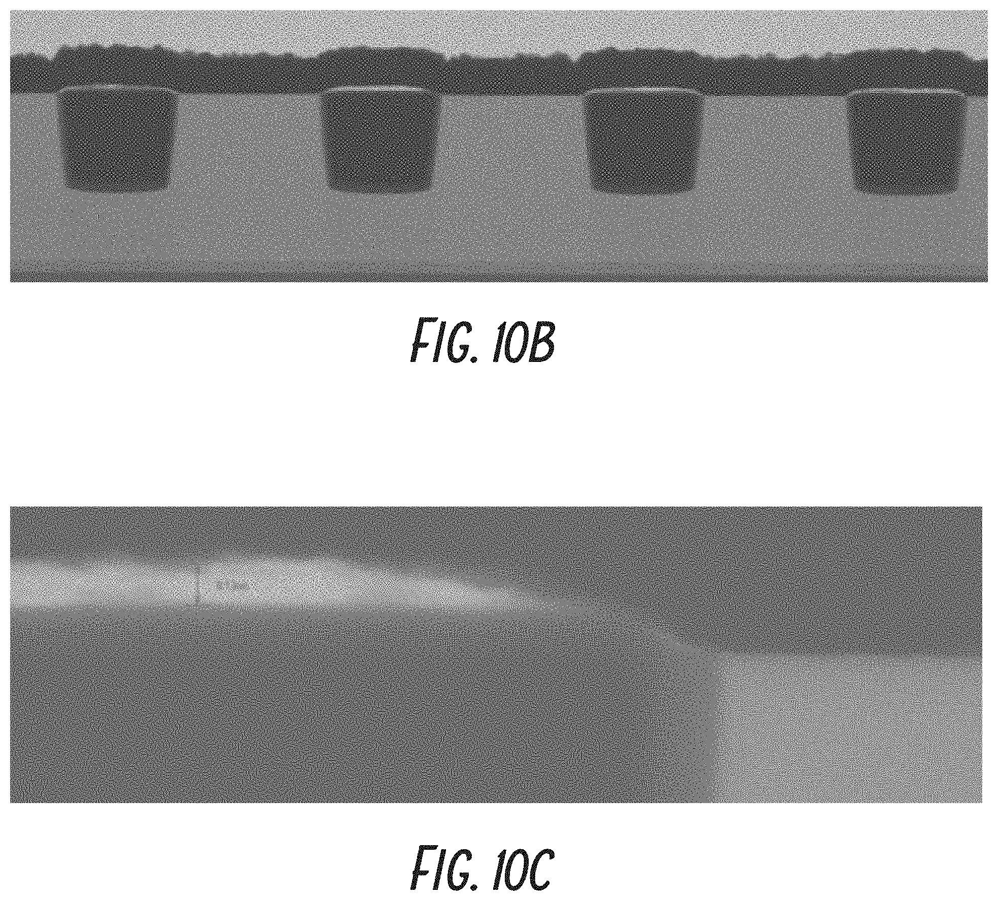
D00013
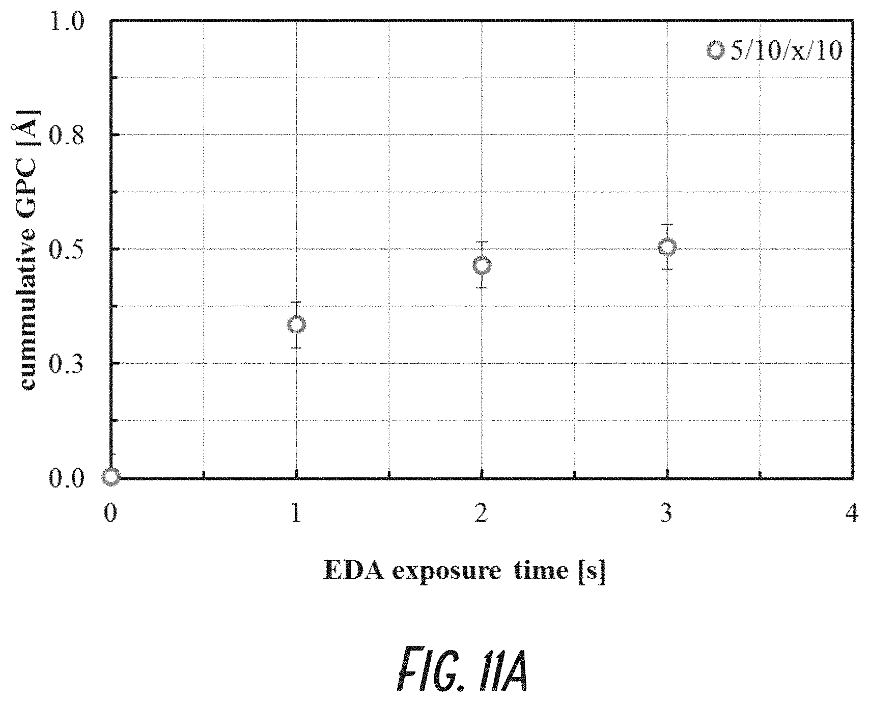
D00014
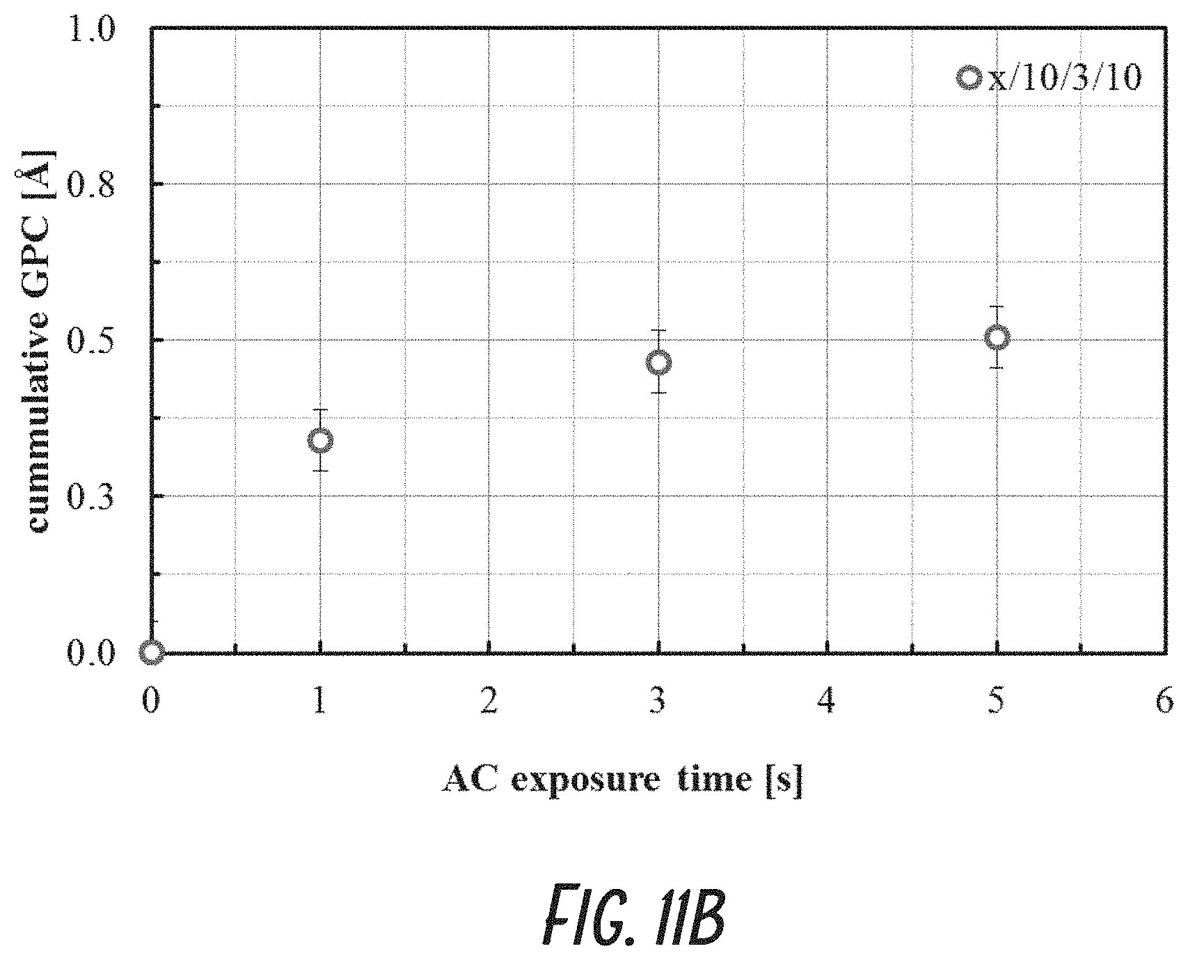
D00015
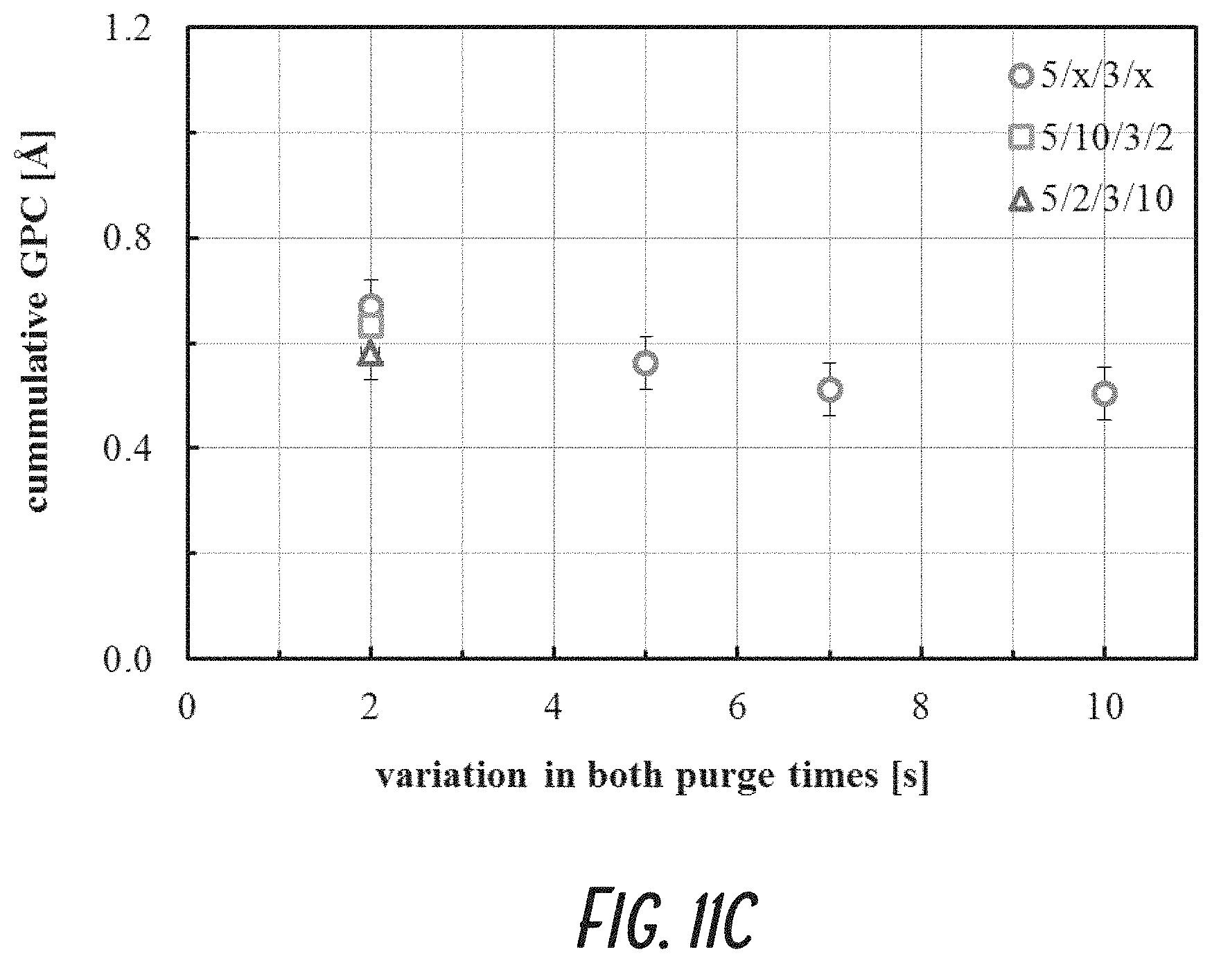
D00016
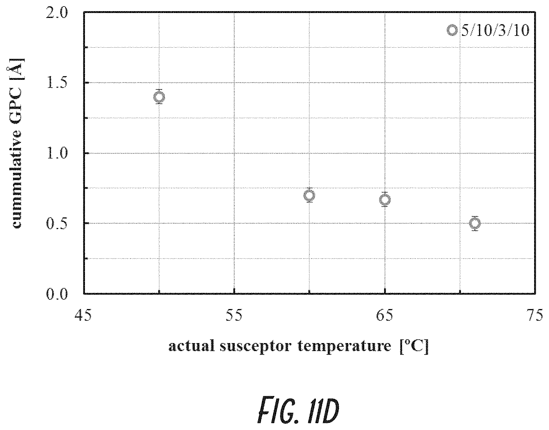
D00017
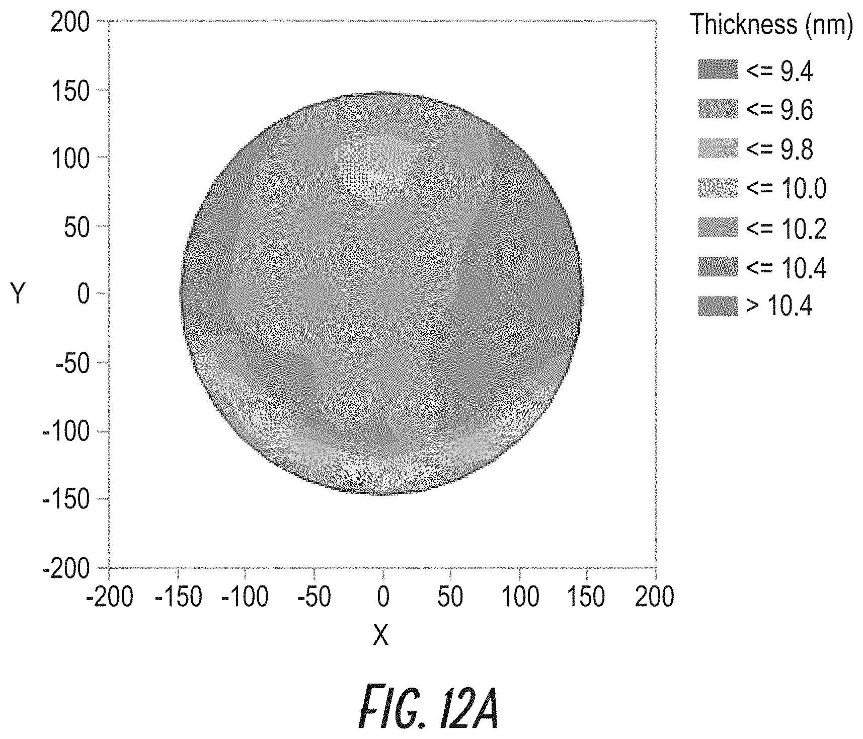
D00018
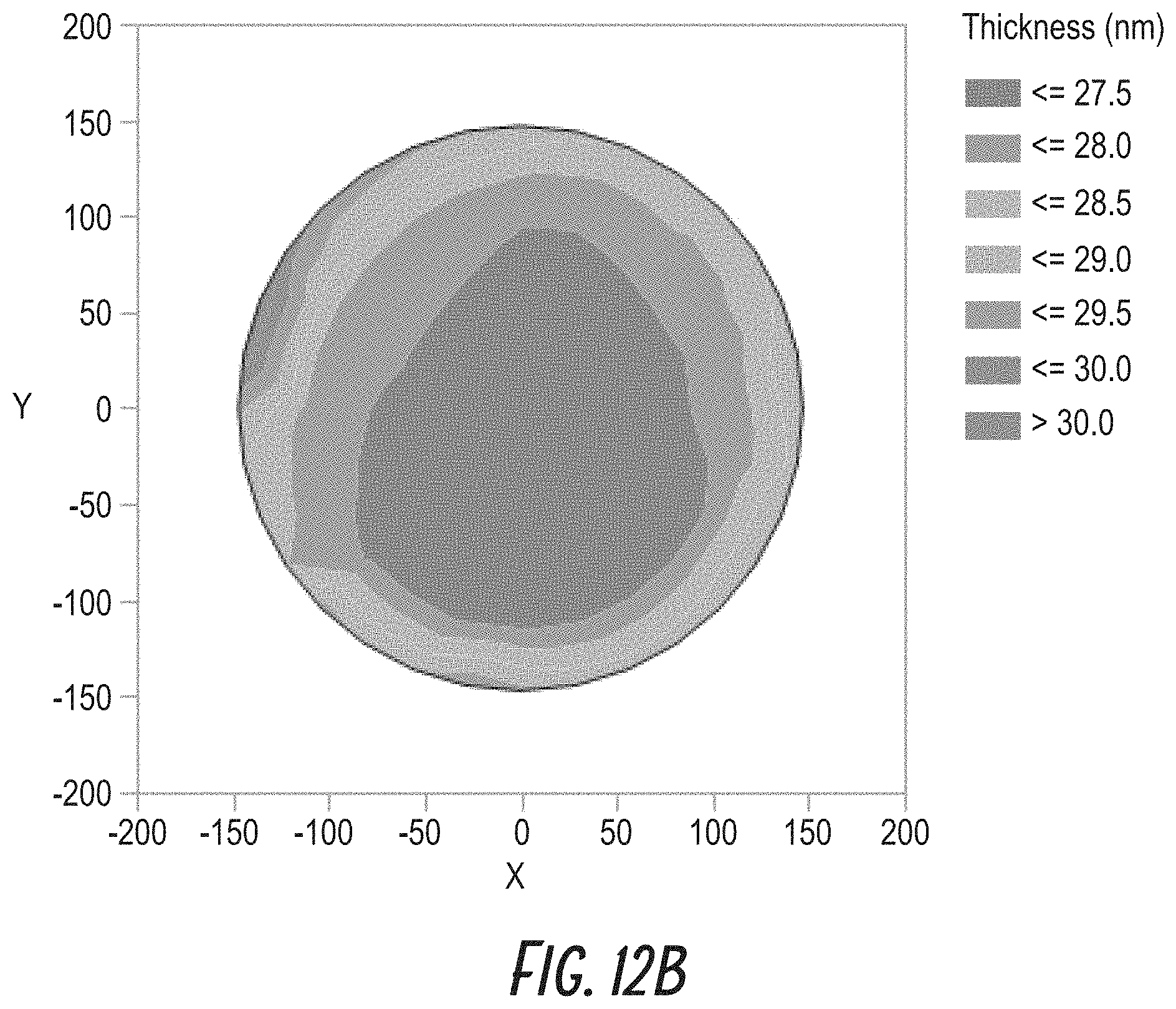
XML
uspto.report is an independent third-party trademark research tool that is not affiliated, endorsed, or sponsored by the United States Patent and Trademark Office (USPTO) or any other governmental organization. The information provided by uspto.report is based on publicly available data at the time of writing and is intended for informational purposes only.
While we strive to provide accurate and up-to-date information, we do not guarantee the accuracy, completeness, reliability, or suitability of the information displayed on this site. The use of this site is at your own risk. Any reliance you place on such information is therefore strictly at your own risk.
All official trademark data, including owner information, should be verified by visiting the official USPTO website at www.uspto.gov. This site is not intended to replace professional legal advice and should not be used as a substitute for consulting with a legal professional who is knowledgeable about trademark law.