Combined anneal and selective deposition process
Maes , et al. Feb
U.S. patent number 10,204,782 [Application Number 15/132,091] was granted by the patent office on 2019-02-12 for combined anneal and selective deposition process. This patent grant is currently assigned to ASM IP HOLDING B.V., IMEC vzw. The grantee listed for this patent is ASM IP Holding B.V., IMEC VZW. Invention is credited to Roel Gronheid, Werner Knaepen, Jan Willem Maes, Arjun Singh.

| United States Patent | 10,204,782 |
| Maes , et al. | February 12, 2019 |
Combined anneal and selective deposition process
Abstract
A method for forming a film with an annealing step and a deposition step is disclosed. The method comprises an annealing step for inducing self-assembly or alignment within a polymer. The method also comprises a selective deposition step in order to enable selective deposition on a polymer.
| Inventors: | Maes; Jan Willem (Wilrijk, BE), Knaepen; Werner (Leuven, BE), Gronheid; Roel (Huldenberg, BE), Singh; Arjun (Leuven, BE) | ||||||||||
|---|---|---|---|---|---|---|---|---|---|---|---|
| Applicant: |
|
||||||||||
| Assignee: | IMEC vzw (Leuven,
BE) ASM IP HOLDING B.V. (Almere, NL) |
||||||||||
| Family ID: | 60038354 | ||||||||||
| Appl. No.: | 15/132,091 | ||||||||||
| Filed: | April 18, 2016 |
Prior Publication Data
| Document Identifier | Publication Date | |
|---|---|---|
| US 20170301542 A1 | Oct 19, 2017 | |
| Current U.S. Class: | 1/1 |
| Current CPC Class: | H01L 21/0337 (20130101); H01L 21/0338 (20130101); H01L 21/32 (20130101); H01L 21/02178 (20130101); H01L 21/0335 (20130101); G03F 7/0002 (20130101); H01L 21/0228 (20130101); H01L 21/0273 (20130101); H01L 21/0332 (20130101) |
| Current International Class: | H01L 21/33 (20060101); G03F 7/00 (20060101); H01L 21/02 (20060101); H01L 21/027 (20060101); H01L 21/32 (20060101); H01L 21/033 (20060101) |
References Cited [Referenced By]
U.S. Patent Documents
| 4863879 | September 1989 | Kwok |
| 4948755 | August 1990 | Mo |
| 5288697 | February 1994 | Schrepp et al. |
| 5447887 | September 1995 | Filipiak et al. |
| 5633036 | May 1997 | Seebauer et al. |
| 5869135 | February 1999 | Vaeth et al. |
| 5925494 | July 1999 | Horn |
| 6046108 | April 2000 | Liu et al. |
| 6482740 | November 2002 | Soininen et al. |
| 6586330 | July 2003 | Ludviksson et al. |
| 6679951 | January 2004 | Soininen et al. |
| 6759325 | July 2004 | Raaijmakers et al. |
| 6811448 | November 2004 | Paton et al. |
| 6844258 | January 2005 | Fair et al. |
| 6878628 | April 2005 | Sophie et al. |
| 6887795 | May 2005 | Soininen et al. |
| 6921712 | July 2005 | Soininen et al. |
| 6958174 | October 2005 | Klaus et al. |
| 7067407 | June 2006 | Kostamo et al. |
| 7084060 | August 2006 | Furukawa et al. |
| 7118779 | October 2006 | Verghese et al. |
| 7220669 | May 2007 | Hujanen et al. |
| 7241677 | July 2007 | Soininen et al. |
| 7323411 | January 2008 | Blosse |
| 7405143 | July 2008 | Leinikka et al. |
| 7425350 | September 2008 | Todd |
| 7476618 | January 2009 | Kilpela et al. |
| 7494927 | February 2009 | Kostamo et al. |
| 7595271 | September 2009 | White |
| 7754621 | July 2010 | Putkonen |
| 7799135 | September 2010 | Verghese et al. |
| 7910177 | March 2011 | Li |
| 7914847 | March 2011 | Verghese et al. |
| 7927942 | April 2011 | Raaijmakers |
| 7955979 | June 2011 | Kostamo et al. |
| 7964505 | June 2011 | Khandelwal et al. |
| 8293597 | October 2012 | Raaijmakers |
| 8293658 | October 2012 | Shero et al. |
| 8425739 | April 2013 | Wieting |
| 8536058 | September 2013 | Kostamo et al. |
| 8778815 | July 2014 | Yamaguchi et al. |
| 8890264 | November 2014 | Dewey et al. |
| 8956971 | February 2015 | Haukka et al. |
| 8962482 | February 2015 | Albertson et al. |
| 8980418 | March 2015 | Darling et al. |
| 8993404 | March 2015 | Korbrinsky et al. |
| 9067958 | June 2015 | Romero |
| 9112003 | August 2015 | Haukka et al. |
| 9129897 | September 2015 | Pore et al. |
| 9136110 | September 2015 | Rathsack |
| 9159558 | October 2015 | Cheng et al. |
| 9236292 | January 2016 | Romero et al. |
| 9257303 | February 2016 | Haukka et al. |
| 9490145 | November 2016 | Niskanen et al. |
| 9502289 | November 2016 | Haukka et al. |
| 9803277 | October 2017 | Longrie et al. |
| 9911595 | March 2018 | Smith et al. |
| 2001/0019803 | September 2001 | Mirkanimi |
| 2001/0025205 | September 2001 | Chern et al. |
| 2002/0047144 | April 2002 | Nguyen et al. |
| 2002/0068458 | June 2002 | Chiang et al. |
| 2002/0090777 | July 2002 | Forbes et al. |
| 2003/0027431 | February 2003 | Sneh et al. |
| 2003/0066487 | April 2003 | Suzuki |
| 2003/0143839 | July 2003 | Raaijmakers et al. |
| 2003/0181035 | September 2003 | Yoon et al. |
| 2003/0192090 | October 2003 | Meilland |
| 2003/0193090 | October 2003 | Otani |
| 2004/0219746 | July 2004 | Vaartstra et al. |
| 2005/0136604 | June 2005 | Al-Bayati et al. |
| 2005/0223989 | October 2005 | Lee et al. |
| 2006/0019493 | January 2006 | Li |
| 2006/0047132 | March 2006 | Shenai-Khatkhate et al. |
| 2006/0141155 | June 2006 | Gordon et al. |
| 2006/0156979 | July 2006 | Thakur et al. |
| 2006/0199399 | September 2006 | Muscat |
| 2006/0226409 | October 2006 | Burr et al. |
| 2006/0292845 | December 2006 | Chiang et al. |
| 2007/0063317 | March 2007 | Kim et al. |
| 2007/0099422 | May 2007 | Wijekoon et al. |
| 2007/0241390 | October 2007 | Tanaka et al. |
| 2008/0066680 | March 2008 | Sherman |
| 2008/0072819 | March 2008 | Rahtu |
| 2008/0179741 | July 2008 | Streck et al. |
| 2008/0241575 | October 2008 | Lavoie et al. |
| 2008/0282970 | November 2008 | Heys et al. |
| 2009/0035949 | February 2009 | Niinisto et al. |
| 2009/0071505 | March 2009 | Miya et al. |
| 2009/0081385 | March 2009 | Heys et al. |
| 2009/0203222 | August 2009 | Dussarrat et al. |
| 2009/0269507 | October 2009 | Yu et al. |
| 2009/0274887 | November 2009 | Millward |
| 2009/0311879 | December 2009 | Blasco et al. |
| 2010/0015756 | January 2010 | Weidman et al. |
| 2010/0147396 | June 2010 | Yamagishi et al. |
| 2010/0178468 | July 2010 | Jiang et al. |
| 2010/0248473 | September 2010 | Ishizaka et al. |
| 2010/0270626 | October 2010 | Raisanen |
| 2011/0053800 | March 2011 | Jung |
| 2011/0124192 | May 2011 | Ganguli et al. |
| 2011/0221061 | September 2011 | Prakash |
| 2011/0311726 | December 2011 | Liu et al. |
| 2012/0032311 | February 2012 | Gates |
| 2012/0046421 | February 2012 | Darling |
| 2012/0088369 | April 2012 | Weidman et al. |
| 2012/0189868 | July 2012 | Borovik et al. |
| 2012/0219824 | August 2012 | Prolier et al. |
| 2012/0241411 | September 2012 | Darling et al. |
| 2012/0264291 | October 2012 | Ganguli et al. |
| 2012/0269970 | October 2012 | Ido et al. |
| 2013/0005133 | January 2013 | Lee et al. |
| 2013/0089983 | April 2013 | Sugita et al. |
| 2013/0095664 | April 2013 | Matero et al. |
| 2013/0115768 | May 2013 | Pore et al. |
| 2013/0146881 | June 2013 | Yamazaki et al. |
| 2013/0189837 | July 2013 | Haukka et al. |
| 2013/0196502 | August 2013 | Haukka et al. |
| 2013/0203267 | August 2013 | Pomarede et al. |
| 2013/0280919 | October 2013 | Yuasa et al. |
| 2013/0284094 | October 2013 | Pavol et al. |
| 2013/0316080 | November 2013 | Yamaguchi et al. |
| 2014/0001572 | January 2014 | Bohr et al. |
| 2014/0024200 | January 2014 | Kato et al. |
| 2014/0091308 | April 2014 | Dasgupta et al. |
| 2014/0120738 | May 2014 | Jung et al. |
| 2014/0152383 | June 2014 | Nikonov et al. |
| 2014/0190409 | July 2014 | Matsumoto et al. |
| 2014/0193598 | July 2014 | Traser |
| 2014/0205766 | July 2014 | Lyon |
| 2014/0209022 | July 2014 | Inoue et al. |
| 2014/0227461 | August 2014 | Darwish et al. |
| 2014/0273290 | September 2014 | Somervell |
| 2014/0273514 | September 2014 | Somervell |
| 2014/0273523 | September 2014 | Rathsack |
| 2014/0273527 | September 2014 | Niskanen et al. |
| 2015/0004806 | January 2015 | Ndiege et al. |
| 2015/0011032 | January 2015 | Kunimatsu |
| 2015/0037972 | February 2015 | Danek et al. |
| 2015/0064931 | March 2015 | Kumagi et al. |
| 2015/0087158 | March 2015 | Sugita et al. |
| 2015/0093890 | April 2015 | Blackwell et al. |
| 2015/0097292 | April 2015 | He et al. |
| 2015/0118863 | April 2015 | Rathod et al. |
| 2015/0162214 | June 2015 | Thompson et al. |
| 2015/0170961 | June 2015 | Romero et al. |
| 2015/0179798 | June 2015 | Clendenning et al. |
| 2015/0217330 | August 2015 | Haukka et al. |
| 2015/0240121 | August 2015 | Sugita et al. |
| 2015/0299848 | October 2015 | Haukka et al. |
| 2015/0371866 | December 2015 | Chen et al. |
| 2015/0376211 | December 2015 | Girard et al. |
| 2016/0075884 | March 2016 | Chen |
| 2016/0186004 | June 2016 | Hustad |
| 2016/0222504 | August 2016 | Haukka et al. |
| 2016/0247695 | August 2016 | Niskanen et al. |
| 2016/0276208 | September 2016 | Haukka et al. |
| 2016/0293398 | October 2016 | Danek et al. |
| 2016/0365280 | December 2016 | Brink et al. |
| 2017/0037513 | February 2017 | Haukka et al. |
| 2017/0040164 | February 2017 | Wang et al. |
| 2017/0058401 | March 2017 | Blackwell et al. |
| 2017/0069527 | March 2017 | Haukka et al. |
| 2017/0100742 | April 2017 | Pore et al. |
| 2017/0100743 | April 2017 | Pore et al. |
| 2017/0154806 | June 2017 | Wang et al. |
| 2017/0298503 | October 2017 | Maes et al. |
| 2017/0323776 | November 2017 | Farm et al. |
| 2017/0352533 | December 2017 | Tois et al. |
| 2017/0352550 | December 2017 | Tois et al. |
| 2018/0233350 | August 2018 | Tois et al. |
| 0469456 | Feb 1992 | EP | |||
| 0880168 | Nov 1998 | EP | |||
| 1340269 | Feb 2009 | EP | |||
| 2011-187583 | Sep 2011 | JP | |||
| 2014-93331 | May 2014 | JP | |||
| 102001001072 | Feb 2001 | KR | |||
| 1020040056026 | Jun 2004 | KR | |||
| WO 2002/045167 | Jun 2002 | WO | |||
| WO 2011/156705 | Dec 2011 | WO | |||
| WO 2013/161772 | Oct 2013 | WO | |||
| WO 2014/156782 | Oct 2014 | WO | |||
| WO 2014209390 | Dec 2014 | WO | |||
| WO 15/047345 | Apr 2015 | WO | |||
| WO 2015/047345 | Apr 2015 | WO | |||
| WO 2015094305 | Jun 2015 | WO | |||
| WO 2015147843 | Oct 2015 | WO | |||
| WO 2015147858 | Oct 2015 | WO | |||
| WO 17/184357 | Oct 2017 | WO | |||
| WO 2017/184358 | Oct 2017 | WO | |||
Other References
|
Prasittichai et al., "Area Selective Molecular Layer Deposition of Polyurea Film", Applied Materials & Interfaces, 2013, vol. 5, pp. 13391-13396. cited by applicant . Coclite, et al.; 25th Anniversary Article: CVD Polymers: A New Paradigm for Surface Modification and Device Fabrication; Advanced Materials; Oct. 2013; 25; pp. 5392-5423. cited by applicant . Farr, Isaac Vincent; Synthesis and Characterization of Novel Polyimide Gas Separation Membrane Material Systems, Chapter 2; Virginia Tech Chemistry PhD Dissertation; URN # etd-080999-123034; Jul. 26, 1999. cited by applicant . George, Steven M.; Atomic Layer Deposition: An Overview; Chem. Rev. 2010, 110, pp. 111-131; Feb. 12, 2009. cited by applicant . Norrman, et al.; 6 Studies of Spin-Coated Polymer Films; Annu. Rep. Prog. Chem.; Sect. C; 2005; 101; pp. 174-201. cited by applicant . Putkonen, et al.; Atomic Layer Deposition of Polyimide Thin Films; Journal of Materials Chemistry; 2007, 17, pp. 664-669. cited by applicant . Ratta, Varun; Crystallization, Morphology, Thermal Stability and Adhesive Properties of Novel High Performance Semicrystalline Polyimides, Chapter 1; Virginia Tech Chemistry PhD Dissertation; URN # etd-051799-162256; Apr. 26, 1999. cited by applicant . Sapp, et al.; Thermo-Mechanical and Electrical Characterization of Through-Silicon Vias with a Vapor Deposited Polyimide Dielectric Liner; IEEE; 2012. cited by applicant . Sundberg, et al.; Organic and Inorganic-Organic Thin Film Structures by Molecular Layer Deposition: A Review; Beilstein J. Nanotechnol; 2014, 5, pp. 1104-1136. cited by applicant . Toirov, et al.; Thermal Cyclodehydration of Polyamic Acid Initiated by UV-Irradiation; Iranian Polymer Journal; vol. 5, No. 1; pp. 16-22; 1996; Iran. cited by applicant . Zhou, et al.; Fabrication of Organic Interfacial Layers by Molecular Layer Deposition: Present Status and Future Opportunities; Journal of Vacuum Science & Technology; A 31 (4), 040801-1 to 040801-18; 2013. cited by applicant . International Search Report and Written Opinion dated Jun. 16, 2017 in PCT/US2017/026518. cited by applicant . International Search Report and Written Opinion dated Jun. 20, 2017 in PCT/US2017/026515. cited by applicant . International Search Report and Written Opinion dated Jun. 22, 2017 in PCT/US2017/26519. cited by applicant . Au et al., "Selective Chemical Vapor Deposition of Manganese Self-Aligned Capping Layer for Cu Interconnections in Microelectronics", Journal of the Electrochemical Society, vol. 157, No. 6, 2010, pp. D341-D345. cited by applicant . Bouteville et al., "Selective R.T.L.P.C.V.D. of Tungsten by Silane Reduction on Patterned PPQ/Si Wafers" Journal De Physique IV, Colloque C2, suppl. au Journal de Physique II, vol. 1, Sep. 1991, pp. C2-857-C2-864. cited by applicant . Burton, B.B. et al., "Atomic Layer Deposition of MgO Using Bis(ethylcyclopentadienyl)magnesium and H20". J. Phys. Chem. C, 2009, 113, 1939-1946. cited by applicant . Burton, B.B., et al., "Si02 Atomic Layer Deposition Using Tris(dimethylamino)silane and Hydrogen Peroxide Studied by in Situ Transmission FTIR Spectroscopy". J. Phys. Chem. C, 2009, 113, 8249-8257. cited by applicant . Carlsson, J., "Precursor Design for Chemical Vapour Deposition", Acta Chemica Scandinavica, vol. 45, 1991, pp. 864-869. cited by applicant . Chang et al, "Influences of damage and contamination from reactive ion etching on selective tungsten deposition in a low-pressure chemical-vapor-deposition reactor", J. Appl. Phys., vol. 80, No. 5, Sep. 1, 1996, pp. 3056-3061. cited by applicant . Elam et al., "Kinetics of the WF6 and Si2H6 surface reactions during tungsten atomic layer deposition", Surface Science, vol. 479, 2001, pp. 121-135. cited by applicant . Elam et al., "Nucleation and growth during tungsten atomic layer deposition on SiO2 surfaces", Thin Solid Films, vol. 386, 2001 pp. 41-52. cited by applicant . Fabreguette et al., Quartz crystal microbalance study of tungsten atomic layer deposition using WF6 and Si2H6, Thin Solid Films, vol. 488, 2005, pp. 103-110. cited by applicant . Farm et al. Selective-Area Atomic Layer Deposition Using Poly( methyl methacrylate) Films as Mask Layers, J. Phys. Chem. C, 2008, 112, pp. 15791-15795. (Year: 2008). cited by applicant . Ghosal et al., Controlling Atomic Layer Deposition of Ti02 in Aerogels through Surface Functionalization, Chem. Matter, vol. 21, pp. 1989-1992, 2009. cited by applicant . Grubbs et al., "Nucleation and growth during the atomic layer deposition of W on Al2O3 and Al2O3 on W", Thin Solid Films, vol. 467, 2004, pp. 16-27. cited by applicant . Hymes et al., "Surface cleaning of copper by thermal and plasma treatment in reducing and inert ambients", J. Vac. Sci. Technol. B, vol. 16, No. 3, May/Jun. 1998, pp. 1107-1109. cited by applicant . International Search Report and Written Opinion dated Feb. 17, 2012 in Application No. PCT/US2011/039970, filed Jun. 10, 2011. cited by applicant . Klaus et al., "Atomic layer deposition of tungsten using sequential surface chemistry with a sacrificial stripping reaction", Thin Solid Films, vol. 360, 2000, pp. 145-153. cited by applicant . Klaus et al., "Atomically controlled growth of tungsten and tungsten nitride using sequential surface reactions", Applied Surface Science 162-163, 2000, pp. 479-491. cited by applicant . King, Dielectric Barrier, Etch Stop, and Metal Capping Materials for State of the Art and beyond Metal Interconnects, ECS Journal of Solid State Science and Technology, vol. 4, Issue 1, pp. N3029-N3047, 2015. cited by applicant . Lee et al., Area-Selective Atomic Layor Deposition Using Self-Assembled Monolayer and Scanning Probe Lithography, Journal of the Electrochemical Society, vol. 156, Issue 9, pp. G125-G128, 2009. cited by applicant . Lei et al., "Real-time observation and opitimization of tungsten atomic layer deposition process cycle", J. Vac. Sci. Technol. B, vol. 24, No. 2, Mar./Apr. 2006, pp. 780-789. cited by applicant . Lemonds, Andrew Michael, "Atomic Layer Deposition and Properties of Refractory Transition Metal-Based Copper-Diffusion Barriers for ULSI Interconnect", The University of Texas at Austin, 2003, pp. 1-197. cited by applicant . Leusink et al., "Growth kinetics and inhibition of growth of chemical vapor deposited thin tungsten films on silicon from tungsten hexafluoride", J. Appl. Phys., vol. 72, No. 2, Jul. 15, 1992, pp. 490-498. cited by applicant . Liang, Xuehai, et al., "Growth of Ge Nanofilms Using Electrochemical Atomic Layer Deposition, with a "Bait and Switch" Surface-Limited Reaction". Journal of the American Chemical Society, 2011, 133, 8199-8024. cited by applicant . Lohokare et al., "Reactions of Disilane on Cu(111): Direct Observation of Competitive Dissociation, Disproportionation, and Thin Film Growth Processes", Langmuir 1995, vol. 11, pp. 3902-3912. cited by applicant . Low et al., Selective deposition of CVD iron on silicon dioxide and tungsten, Microelectronic Engineering 83, pp. 2229-2233, 2006. cited by applicant . Mackus et al., Influence of Oxygen Exposure on the Nucleation of Platinum Atomic Layer Deposition: Consequences for Film Growth, Nanopatterning, and Nanoparticle Synthesis, Chem. Matter, vol. 25, pp. 1905-1911, 2013. cited by applicant . Mackus et al., Local deposition of high-purity Pt nanostructures by combining electron beam induced deposition and atomic layer deposition, Journal of Applied Physics, vol. 107, pp. 116102-1-116102-3, 2010. cited by applicant . Maluf et al., "Selective tungsten filling of sub-0.25.mu.m trenches for the fabrication of scaled contacts and x-ray masks", J. Vac. Sci. Technol. B, vol. 8, No. 3, May/Jun. 1990, pp. 568-569. cited by applicant . Notice of Allowance dated Apr. 5, 2017 in U.S. Appl. No. 15/177,195. cited by applicant . Office Action dated Aug. 29, 2014 in U.S. Appl. No. 13/702,992. cited by applicant . Office Action dated Nov. 7, 2014 in U.S. Appl. No. 13/708,863. cited by applicant . Office Action dated Jun. 8, 2017 in Korean Application No. 2013-7000596. cited by applicant . Overhage et al., Selective Atomic Layer Deposition (SALD) of Titanium Dioxide on Silicon and Copper Patterned Substrates, Journal of Undergraduate Research 4, 29, Mar. 2011 in 4 pages. cited by applicant . Parulekar et al., Atomic Layer Deposition of Zirconium Oxide on Copper Patterned Silicon Substrate, Journal of Undergraduate Research, vol. 7, pp. 15-17, 2014. cited by applicant . Parulekar et al., Selective atomic layer deposition of zirconium oxide on copper patterned silicon substrate, pp. 1-6, 2013. cited by applicant . Proslier et al., "Atomic Layer Deposition and Superconducting Properties of NbSi Films", The Journal of Physical Chemistry C, 2011, vol. 115, No. 50, pp. 1-26. cited by applicant . Roberts et al., "Selective Mn deposition on Cu lines", poster presentation, 12th International Conference on Atomic Layer Deposition, Jun. 19, 2012, Dresden, Germany. cited by applicant . Schmei er, Decomposition of formic acid, Chemnitz University of Technology, pp. 1-13, Aug. 31, 2011. cited by applicant . Schmei er, Reduction of Copper Oxide by Formic Acid an ab-initio study, Chemnitz University of Technology, pp. 1-42, Sep. 2011. cited by applicant . Selvaraj et al., Selective atomic layer deposition of zirconia on copper patterned silicon substrates using ethanol as oxygen source as well as copper reductant, Journal of Vacuum Science & Technology A, vol. 32, No. 1, pp. 010601-1 - 010601-4, Jan. 2014. cited by applicant . Senesky et al., "Aluminum nitride as a masking material for the plasma etching of silicon carbide structures," 2010, IEEE, pp. 352-355. cited by applicant . "Tungsten and Tungsten Silicide Chemical Vapor Deposition", TimeDomain CVD, Inc., retrieved from link: http://www.timedomaincvd.com/CVD_Fundamentals/films/W_WSi.html, Last modified Jul. 11, 2008. cited by applicant . Yu et al., "Gas/surface reactions in the chemical vapor deposition of tungsten using WF6/SiH4 mixtures", J. Vac. Sci. Technol. A, vol. 7, No. 3, May/Jun. 1989, pp. 625-629. cited by applicant . Vallat et al., Selective deposition of Ta205 by adding plasma etching super-cycles in plasma enhanced atomic layer deposition steps, Journal of Vacuum Science & Technology A, vol. 35, No. 1, pp. 01B104-1-01B104-7, Jan. 2017. cited by applicant . Vervuurt et al. Area-selective atomic layer deposition of platinum using photosensitive polyimide. Nanotechnology 27 (2016) 405302 (6pp). cited by applicant . Suntola, "Handbook of Crystal Growth. vol. 3., Thin Films and Epitaxy, Part B: Growth mechanisms and Dynamics", Amsterdam: North Holland, Elsevier Science Publishers (1994), Chapter 14, pp. 601-663. cited by applicant . Chen et al. Highly Stable Monolayer Resists for Atomic Layer Deposition on Germanium and Silicon, Chem. Matter. 2006:18:3733-3741. cited by applicant . Mackus et al. The use of atomic layer deposition in advanced nanopatterning. Nanoscale, 2014, 6, pp. 10941-10960. (Year: 2014). cited by applicant . Schuisky et al. Atomic layer deposition of thin films using O2 as oxygen source. Langmuir, 2001, 17, pp. 5508-5512. (Year: 2001). cited by applicant . Bernal-Ramos, et al., "Atomic Layer Deposition of Cobalt Silicide Thin Films Studied by in Situ Infrared Spectroscopy", Chem. Mater. 2015, 27, pp. 4943-4949. cited by applicant . Ellinger et al., "Selective Area Spatial Atomic Layer Deposition of ZnO, Al2O3, and Aluminum-Doped ZnO Using Poly(vinyl pyrrolidone)", Chem Mater. 2014, 26:1514-1522. cited by applicant. |
Primary Examiner: Everhart; Caridad
Assistant Examiner: Singal; Ankush
Attorney, Agent or Firm: Knobbe, Martens, Olson & Bear LLP
Claims
What is claimed is:
1. A method of selectively forming a film comprising: providing a substrate for processing in a reaction chamber, the substrate having at least one polymer layer disposed on the substrate; performing an annealing step on the substrate; and performing a film deposition at a temperature lower than a temperature of the annealing step by sequentially pulsing a first precursor and a second precursor onto the substrate, the film deposition being configured to enable infiltration of at least the first precursor into the at least one polymer layer, wherein an excess of the first precursor and the second precursor are purged from the reaction chamber; wherein a film forms on the at least one polymer from the first precursor; and wherein the film deposition comprises: pulsing the first precursor onto the substrate; purging the first precursor from the reaction chamber; pulsing the second precursor onto the substrate; and purging the second precursor from the reaction chamber.
2. The method of claim 1, wherein a film forms within the at least one polymer from the first precursor that infiltrates the at least one polymer.
3. The method of claim 1, wherein the film comprises at least one of: aluminum oxide (Al.sub.2O.sub.3), silicon dioxide (SiO.sub.2), silicon nitride (SiN), silicon oxynitride (SiON), silicon carbonitride (SiCN), aluminum nitride (AlN), titanium nitride (TiN), tantalum nitride (TaN), tungsten (W), cobalt (Co), titanium dioxide (TiO.sub.2), tantalum oxide (Ta.sub.2O.sub.5), zirconium dioxide (ZrO.sub.2), or hafnium dioxide (HfO.sub.2).
4. The method of claim 2, wherein the film comprises at least one of: aluminum oxide (Al.sub.2O.sub.3), silicon dioxide (SiO.sub.2), silicon nitride (SiN), silicon oxynitride (SiON), silicon carbonitride (SiCN), aluminum nitride (AlN), titanium nitride (TiN), tantalum nitride (TaN), tungsten (W), cobalt (Co), titanium dioxide (TiO.sub.2), tantalum oxide (Ta.sub.2O.sub.5), zirconium dioxide (ZrO.sub.2), or hafnium dioxide (HfO.sub.2).
5. The method of claim 1, wherein during the annealing step, a temperature of the reaction chamber ranges between 100.degree. C. and 400.degree. C.
6. The method of claim 1, wherein during the film deposition, the temperature of the reaction chamber ranges between 25.degree. C. and 300.degree. C.
7. The method of claim 1, wherein the at least one polymer comprises at least one of: poly(methyl methacrylate) (PMMA), polystyrene, poly(styrene-block-methyl methacrylate) (PS-b-PMMA), or an extreme UV photoresist.
8. The method of claim 1, wherein the substrate comprises a second polymer.
9. The method of claim 8, wherein the second polymer comprises at least one of: poly(methyl methacrylate) (PMMA), polystyrene, poly(styrene-block-methyl methacrylate) (PS-b-PMMA), or an extreme UV photoresist.
10. The method of claim 1, wherein purging the excess of the first precursor comprises purging the reaction chamber with at least one of: nitrogen (N.sub.2), argon (Ar), helium (He), or an inert gas.
11. The method of claim 1, wherein the performing the film deposition step is repeated in order to form the film of a greater thickness with each repetition.
12. The method of claim 1, wherein the annealing step and the film deposition take place within a single reaction chamber.
13. A method of selectively forming a film comprising: providing a substrate for processing in a reaction chamber, the substrate having at least one polymer layer disposed on the substrate; performing an annealing step on the substrate; and performing a film deposition by sequentially pulsing a first precursor and a second precursor onto the substrate, the film deposition being configured to enable infiltration of at least the first precursor into the at least one polymer layer, wherein an excess of the first precursor and the second precursor are purged from the reaction chamber; wherein a film forms on the at least one polymer from the first precursor, and wherein the annealing step and the film deposition take place within different reaction chambers located on the same cluster tool.
14. The method of claim 1, wherein the reaction chamber is a batch system for processing substrates.
15. The method of claim 1, wherein the reaction chamber is configured to process multiple substrates.
16. The method of claim 1, wherein the annealing step is configured to induce self-assembly within the at least one polymer layer.
17. The method of claim 1, wherein the temperature of the annealing step is at least 25.degree. C. higher than the temperature of the film deposition.
18. A method of selectively forming a film comprising: providing a substrate for processing in a reaction chamber, the substrate having at least one polymer layer disposed on the substrate; performing a film deposition by sequentially pulsing a first precursor and a second precursor onto the substrate, the film deposition being configured to enable infiltration of at least the first precursor into the at least one polymer layer, wherein an excess of the first precursor and the second precursor are purged from the reaction chamber; and after performing the film deposition, performing an annealing step on the substrate at a temperature higher than a temperature of the film deposition; wherein a film forms on the at least one polymer from the first precursor; and wherein the film deposition comprises: pulsing the first precursor onto the substrate; purging the first precursor from the reaction chamber; pulsing the second precursor onto the substrate; and purging the second precursor from the reaction chamber.
19. The method of claim 18, wherein the annealing step and the film deposition take place within a single reaction chamber.
20. A method of selectively forming a film comprising: providing a substrate for processing in a reaction chamber, the substrate having at least one polymer layer disposed on the substrate; performing a film deposition by sequentially pulsing a first precursor and a second precursor onto the substrate, the film deposition being configured to enable infiltration of at least the first precursor into the at least one polymer layer, wherein an excess of the first precursor and the second precursor are purged from the reaction chamber; and after performing the film deposition, performing an annealing step on the substrate, wherein a film forms on the at least one polymer from the first precursor, wherein the annealing step and the film deposition take place within different reaction chambers located on the same cluster tool.
21. The method of claim 18, wherein the reaction chamber is a batch system for processing substrates.
22. The method of claim 18, wherein the reaction chamber is configured to process multiple substrates.
23. The method of claim 18, wherein the annealing step is configured to induce self-assembly within the at least one polymer layer.
24. The method of claim 18, wherein the temperature of the annealing step is at least 25.degree. C. higher than the temperature of the film deposition.
Description
CROSS-REFERENCE TO RELATED APPLICATION
This application is related to U.S. Non-Provisional patent application Ser. No. 15/132,084, filed Apr. 18, 2016 and entitled "COMBINED ANNEAL AND SELECTIVE DEPOSITION SYSTEMS," and U.S. Provisional Patent Application 62/324,255, filed Apr. 18, 2016 and entitled "METHOD OF FORMING A DIRECTED SELF-ASSEMBLED LAYER ON A SUBSTRATE," the disclosures of which are hereby incorporated by reference in their entireties.
FIELD
The present disclosure generally relates to processes and systems for manufacturing electronic devices. More particularly, the disclosure relates to selective deposition of films. Specifically, the disclosure may disclose methods and systems to selectively form films using a directed self-assembly (DSA) patterning technique.
BACKGROUND
As the trend has pushed semiconductor devices to smaller and smaller sizes, different patterning techniques have arisen. These techniques include spacer defined quadruple patterning, extreme ultraviolet lithography (EUV), and EUV combined with Spacer Defined Double patterning. These approaches have allowed production of nodes in the 7 nm range.
Directed self-assembly (DSA) has been considered as an option for future lithography applications. DSA involves the use of block copolymers to define patterns for self-assembly. The block copolymers used may include poly(methyl methacrylate) (PMMA), polystyrene, or poly(styrene-block-methyl methacrylate) (PS-b-PMMA). Other block copolymers may include emerging "high-Chi" polymers, which may potentially enable small dimensions.
DSA can be used to form parallel lines or regular arrays of holes/pillars/posts with very small pitch and critical dimensions. In particular, DSA can define sub-20 nm patterns through self-assembly, while guided by surface topography and/or surface chemical patterning. As a result, a DSA polymer layer can be infiltrated with a precursor, or a film may be deposited selectively on one of the polymers of the DSA layers.
However, the DSA technique has several drawbacks. In particular, DSA polymers, such as PMMA or polystyrene, have low etch resistance. This makes the transfer of the pattern to layers below more difficult. The issue of low etch resistance becomes greater when the advanced polymers needed to further downscale the size of the semiconductor device has an even lower etch resistance and etch selectivity. In addition, the DSA may result in a high line edge roughness in the obtained patterns. Another drawback is that the obtained structure of parallel lines or array of holes may have some defects at random locations.
As a result, a method for selectively forming a film with higher etching resistance and etching selectivity is desired.
SUMMARY
In accordance with at least one embodiment of the invention, a method to selectively form a film is disclosed. The method comprises: providing a substrate for processing in a reaction chamber, the substrate having at least one polymer layer disposed on the substrate; performing an annealing step on the substrate; and performing a film deposition by sequentially pulsing a first precursor and a second precursor onto the substrate, the film deposition being configured to enable infiltration of at least the first precursor into the at least one polymer layer, wherein an excess of the first precursor and the second precursor are purged from the reaction chamber; wherein a film forms on the at least one polymer from the first precursor.
In accordance with at least one embodiment of the invention, a method for selectively forming a film is disclosed. The method may comprise: providing a substrate for processing in a reaction chamber, the substrate having at least one polymer layer disposed on the substrate; performing a film deposition by sequentially pulsing a first precursor and a second precursor onto the substrate, the film deposition being configured to enable infiltration of at least the first precursor into the at least one polymer layer, wherein an excess of the first precursor and the second precursor are purged from the reaction chamber; and performing an annealing step on the substrate; wherein a film forms on the at least one polymer from the first precursor.
For purposes of summarizing the invention and the advantages achieved over the prior art, certain objects and advantages of the invention have been described herein above. Of course, it is to be understood that not necessarily all such objects or advantages may be achieved in accordance with any particular embodiment of the invention. Thus, for example, those skilled in the art will recognize that the invention may be embodied or carried out in a manner that achieves or optimizes one advantage or group of advantages as taught or suggested herein without necessarily achieving other objects or advantages as may be taught or suggested herein.
All of these embodiments are intended to be within the scope of the invention herein disclosed. These and other embodiments will become readily apparent to those skilled in the art from the following detailed description of certain embodiments having reference to the attached FIGURES, the invention not being limited to any particular embodiment(s) disclosed.
BRIEF DESCRIPTION OF THE DRAWINGS
These and other features, aspects, and advantages of the invention disclosed herein are described below with reference to the drawings of certain embodiments, which are intended to illustrate and not to limit the invention.
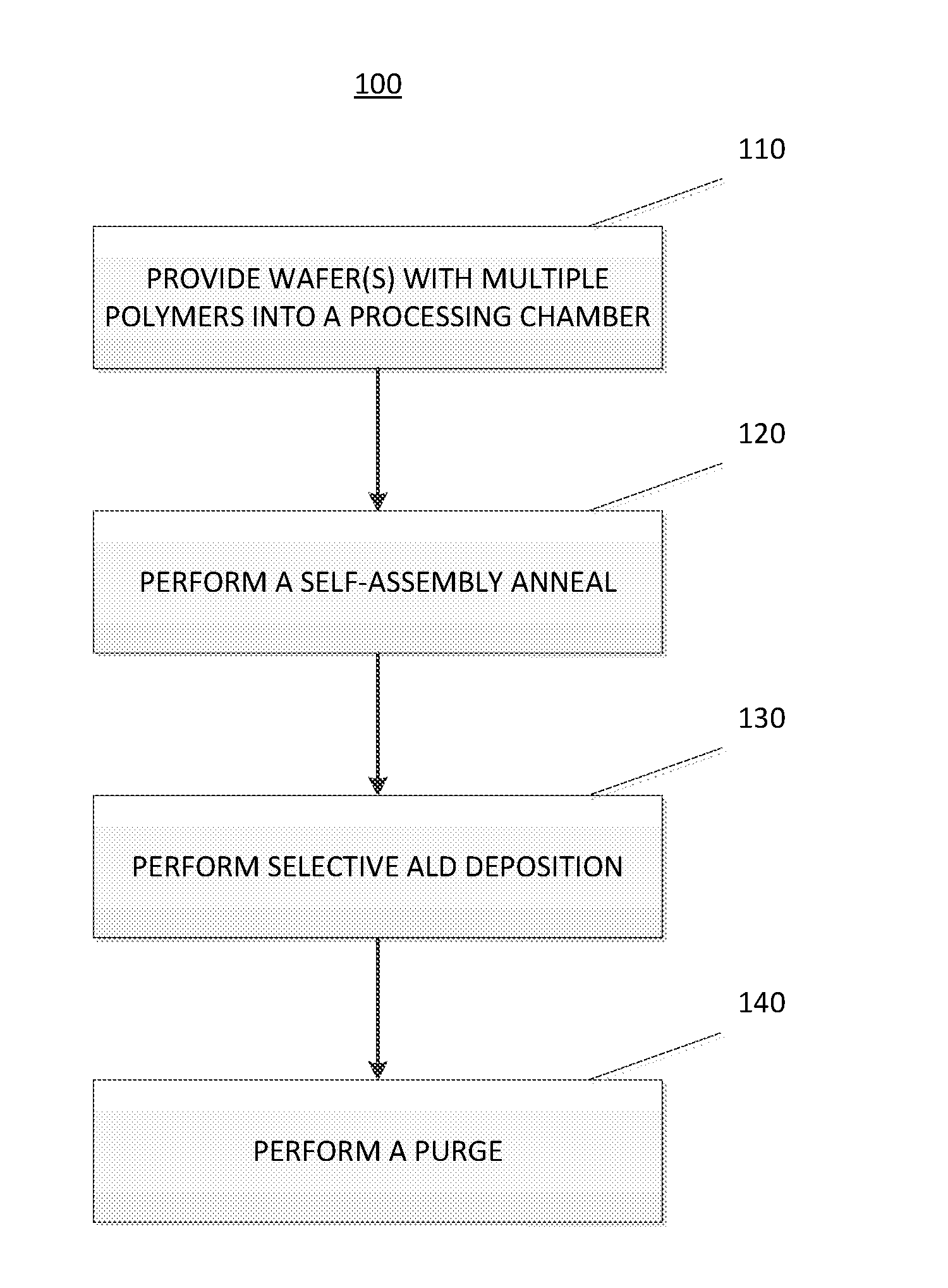
FIG. 1 is a flowchart of a method in accordance with at least one embodiment of the invention.
It will be appreciated that elements in the figures are illustrated for simplicity and clarity and have not necessarily been drawn to scale. For example, the dimensions of some of the elements in the FIGURES may be exaggerated relative to other elements to help improve understanding of illustrated embodiments of the present disclosure.
DETAILED DESCRIPTION
Although certain embodiments and examples are disclosed below, it will be understood by those in the art that the invention extends beyond the specifically disclosed embodiments and/or uses of the invention and obvious modifications and equivalents thereof. Thus, it is intended that the scope of the invention disclosed should not be limited by the particular disclosed embodiments described below.
Embodiments in accordance with the invention relate to the combination of DSA techniques with selective deposition. This combination can increase the etch resistance of polymers significantly. Selective deposition allows for particular polymers to be reacted with a precursor gas, while leaving other polymers untouched.
Combining selective deposition with DSA patterning may provide benefits previously unseen with prior approaches, such as the one described in US Patent Publication No. US 2014/0273514 A1. For example, a selective deposition of aluminum oxide (Al.sub.2O.sub.3) at 90.degree. C. may allow the reaction with a PMMA polymer, while leaving a polystyrene polymer untouched. The aluminum oxide will not only deposit on top of the PMMA polymer, but may be infused into the PMMA polymer to increase the rigidity of the PMMA polymer.
FIG. 1 illustrates a method 100 in accordance with at least one embodiment of the invention. The method 100 includes a first step 110 of providing a wafer with multiple polymers in a processing chamber. As described above, the wafer may have at least a first DSA polymer and a second DSA polymer, wherein the first DSA polymer and the second DSA polymer may be made of PMMA, polystyrene (PS), among other polymers. The processing chamber may be a batch reactor or a cluster tool with two batch reactors. One example of a potential processing chamber may include an A412 system from ASM International N.V., which may run in two reactor chambers the same process or run two different processes independently or sequentially.
The method 100 may include a second step 120 of performing a self-assembly anneal of the DSA polymers. The purpose of the annealing process is to incite the self-assembly or self-organization in the DSA polymers or the block copolymer. In other words, parallel lines or grids of holes/pillars/posts in the polymers may be formed as directed by guidance structures on the substrate. In accordance with at least one embodiment of the invention, this may mean that domains of PMMA and domains of PS may be formed in an alternating manner. The benefits achieved by the self-assembly anneal may include improvement of the self-assembly process, reduction of defects, improved line width roughness, and improved critical dimension (CD) uniformity. Alternatively, the anneal of the second step 120 may have a purpose of degassing moisture or other contaminants from the polymer, hardening the polymer, or selectively burning away one of the polymer types from the substrate surface.
In order to reach a low defect density in the obtained pattern, process parameters, such as the time, temperature, and the ambient conditions and pressure of the annealing process, are critical. A long annealing time may be needed to obtain a low defect density. The anneal may take place at a temperature ranging between 100.degree. C. and 400.degree. C., preferably between 200.degree. C. and 300.degree. C., and most preferably 250.degree. C., for about 60 minutes. Other temperatures and durations are possible depending on the amount of anneal desired. However, the temperature of the self-assembly anneal should not be increased too high or the polymers may start to decompose.
The ambient environment in which the annealing is done may comprise nitrogen, argon, helium, hydrogen, oxygen, ozone, water vapor, solvent vapors, or mixtures of these gases. The pressure of the anneal ambient environment can be any pressure in the range from ultra-high vacuum to atmospheric pressure or even above atmospheric pressure.
In accordance with one embodiment of the invention, the annealing process may take place on a single wafer hot plate. In accordance with another embodiment of the invention, a batch reactor may prove to be beneficial for processes needing a long anneal time. The batch reactor may hold between 2 and 250 substrates, preferably between 5 and 150 substrates, or most preferably about 100 substrates. For example, the A412 may be operated such that one reactor may be used for an anneal process. This may enable to perform long anneals on the order of 1-2 hours in a cost effective way.
The method 100 may also include a third step 130 of performing a selective deposition of a metal or a dielectric film on top of either the first DSA polymer or the second DSA polymer. As such, the selective deposition may be done in a way that the deposited film may react selectively with only one of the two polymers. For example, the selective deposition may take place such that the deposited film may react with PMMA polymer and not PS polymer. In accordance with at least one embodiment of the invention, the third step 130 may comprise an atomic layer deposition of the metal or dielectric film.
Furthermore, the selective deposition may be done such that the deposited metal or dielectric film may infiltrate a polymer, while also depositing a second film on the whole volume of the polymer domain. In accordance with at least one embodiment of the invention, the third step 130 may take place in one reactor of an A412 system, such that the second step 120 takes place in the other reactor of the A412 system. It may also be possible that the second step 120 and the third step 130 take place in one single reactor of the A412 system.
The metal or dielectric deposited in the third step 130 may comprise aluminum oxide (Al.sub.2O.sub.3), silicon dioxide (SiO.sub.2), silicon nitride (SiN), silicon oxycarbide (SiOC), silicon carbonitride (SiCN), aluminum nitride (AlN), titanium nitride (TiN), tantalum nitride (TaN), tungsten (W), cobalt (Co), titanium dioxide (TiO.sub.2), tantalum oxide (Ta.sub.2O.sub.5), zirconium dioxide (ZrO.sub.2), or hafnium dioxide (HfO.sub.2). In order to perform the selective deposition, precursors to obtain the metal may be used, such as trimethylaluminum (TMA) and water (H.sub.2O) for the formation of Al.sub.2O.sub.3.
The selective deposition in the third step 130 may take place at a temperature ranging between 25.degree. C. and 300.degree. C., with a preferable temperature range of 70.degree. C.-90.degree. C. for the formation of Al.sub.2O.sub.3. The temperature during the third step 130 may be less than the temperature during the second step 120, so a cooldown step may be needed to go from an example annealing temperature of 250.degree. C. to a third step 130 temperature of 70.degree. C. In accordance with at least one embodiment of the invention, a temperature of the second step 120 is at least 25.degree. C. higher than that of the third step 130, preferably between 25.degree. C.-300.degree. C. higher than that of the third step 130, or more preferably between 100.degree. C.-250.degree. C. higher than that of the third step 130.
The third step 130 may comprise a first pulse of a first precursor, such as TMA, for a duration ranging from 30 seconds to 10 minutes. The third step 130 may also then comprise a purge for a duration ranging from 10 to 60 seconds. The third step 130 may then comprise a pulse of a second precursor, such as water, for a duration ranging from 10 to 60 seconds. The third step 130 may then comprise a second purge having a duration ranging from 10 seconds to 2 minutes. In addition, the third step 130 may be repeated as needed in order to obtain sufficient deposition of the metal.
In accordance with at least one embodiment of the invention, the third step 130 of film deposition may precede the second step 120 of annealing. In this case, the metal or dielectric film may first infiltrate the polymer, and then an annealing process may occur. As a result of the annealing process, polymer that did not react with the metal or dielectric film during the third step 130 may be burned away in the second step 120.
The method 100 may also include a fourth step 140 of purging the precursors. The fourth step 140 may involve introduction of a purge gas such as nitrogen, helium, argon, and other inert gases. The purge gas would remove excess precursor from the fourth step 140 from the processing chamber. The fourth step 140 may take place at a temperature similar to those of the third step 130.
In accordance with at least one embodiment of the invention, the third step 130 may be repeated as necessary in order to allow the precursors to infiltrate into the DSA polymer. The cycle may be repeated approximately 5 times to ensure sufficient amount of the metal or dielectric film in the DSA polymer. In each cycle, the time duration of the third step 130 may be on the order of a few minutes. With these time durations, a batch reactor may be used to achieve high productivity and low process costs by processing up to 100 wafers or more at a time.
In accordance with at least one embodiment of the invention, the method 100 may be operated such that the third step 130 may be repeated in a pulse-purge-pulse-purge manner. The conditions of these steps may be set at higher pressure and a longer time in order to allow the precursors to infiltrate the polymers. A single cycle in this manner may range between 1 and 20 minutes in duration. The cycle may be repeated several times, typically five times, in order to obtain sufficient deposition of the material inside the polymer. Because infiltration of the material inside the polymer may take a longer amount of time, a combined annealing and deposition process provides an opportunity to perform steps in a batch manner.
A potential application for use of a combined annealing and selective deposition process may be for extreme ultraviolet (EUV) photoresist. The annealing for a EUV application may not be for the self-assembly of the polymer, but may serve a curing or stabilizing purpose. For example, the combined annealing and selective deposition process in accordance with at least one embodiment of the invention may assist in the sequential infiltration synthesis (SIS) step as potentially preventing conversion of carboxyl groups, or by degassing moisture from the polymer film or by stabilizing or hardening the photoresist.
The particular implementations shown and described are illustrative of the invention and its best mode and are not intended to otherwise limit the scope of the aspects and implementations in any way. Indeed, for the sake of brevity, conventional manufacturing, connection, preparation, and other functional aspects of the system may not be described in detail. Furthermore, the connecting lines shown in the various FIGURES are intended to represent exemplary functional relationships and/or physical couplings between the various elements. Many alternative or additional functional relationship or physical connections may be present in the practical system, and/or may be absent in some embodiments.
It is to be understood that the configurations and/or approaches described herein are exemplary in nature, and that these specific embodiments or examples are not to be considered in a limiting sense, because numerous variations are possible. The specific routines or methods described herein may represent one or more of any number of processing strategies. Thus, the various acts illustrated may be performed in the sequence illustrated, in other sequences, or omitted in some cases.
The subject matter of the present disclosure includes all novel and nonobvious combinations and subcombinations of the various processes, systems, and configurations, and other features, functions, acts, and/or properties disclosed herein, as well as any and all equivalents thereof.
* * * * *
References
D00000
D00001
XML
uspto.report is an independent third-party trademark research tool that is not affiliated, endorsed, or sponsored by the United States Patent and Trademark Office (USPTO) or any other governmental organization. The information provided by uspto.report is based on publicly available data at the time of writing and is intended for informational purposes only.
While we strive to provide accurate and up-to-date information, we do not guarantee the accuracy, completeness, reliability, or suitability of the information displayed on this site. The use of this site is at your own risk. Any reliance you place on such information is therefore strictly at your own risk.
All official trademark data, including owner information, should be verified by visiting the official USPTO website at www.uspto.gov. This site is not intended to replace professional legal advice and should not be used as a substitute for consulting with a legal professional who is knowledgeable about trademark law.