Structure and method for integrated circuits packaging with increased density
Woychik , et al. A
U.S. patent number 10,381,326 [Application Number 14/289,483] was granted by the patent office on 2019-08-13 for structure and method for integrated circuits packaging with increased density. This patent grant is currently assigned to Invensas Corporation. The grantee listed for this patent is Invensas Corporation. Invention is credited to Andrew Cao, Bong-Sub Lee, Arkalgud R. Sitaram, Charles G. Woychik.


View All Diagrams
| United States Patent | 10,381,326 |
| Woychik , et al. | August 13, 2019 |
Structure and method for integrated circuits packaging with increased density
Abstract
A method of forming a semiconductor package comprises forming one or more first vias in a first side of a substrate and attaching a first side of a first microelectronic element to the first side of the substrate. The first microelectronic element is electrically coupled to at least one of the one or more first vias. The method further comprise obtaining a second microelectronic element including one or more second vias in a first side of the second microelectronic element, and attaching a second side of the substrate to the first side of the second microelectronic element. The second microelectronic element is electrically coupled to at least one of the one or more first vias. Each of one or more connecting elements has a first end attached to a first side of the second microelectronic element and a second end extends beyond a second side of the first microelectronic element.
| Inventors: | Woychik; Charles G. (San Jose, CA), Sitaram; Arkalgud R. (Cupertino, CA), Cao; Andrew (Fremont, CA), Lee; Bong-Sub (Mountain View, CA) | ||||||||||
|---|---|---|---|---|---|---|---|---|---|---|---|
| Applicant: |
|
||||||||||
| Assignee: | Invensas Corporation (San Jose,
CA) |
||||||||||
| Family ID: | 53373639 | ||||||||||
| Appl. No.: | 14/289,483 | ||||||||||
| Filed: | May 28, 2014 |
Prior Publication Data
| Document Identifier | Publication Date | |
|---|---|---|
| US 20150348940 A1 | Dec 3, 2015 | |
| Current U.S. Class: | 1/1 |
| Current CPC Class: | H01L 21/6835 (20130101); H01L 23/3731 (20130101); H01L 23/367 (20130101); H01L 24/92 (20130101); H01L 25/03 (20130101); H01L 21/76898 (20130101); H01L 23/29 (20130101); H01L 24/02 (20130101); H01L 25/50 (20130101); H01L 21/561 (20130101); H01L 25/18 (20130101); H01L 25/0652 (20130101); H01L 25/0657 (20130101); H01L 24/14 (20130101); H01L 24/94 (20130101); H01L 21/56 (20130101); H01L 23/3128 (20130101); H01L 23/3107 (20130101); H01L 23/481 (20130101); H01L 24/17 (20130101); H01L 24/97 (20130101); H01L 24/13 (20130101); H01L 2224/05568 (20130101); H01L 2224/94 (20130101); H01L 2224/131 (20130101); H01L 2224/13124 (20130101); H01L 2924/18161 (20130101); H01L 2224/13147 (20130101); H01L 2224/97 (20130101); H01L 2225/06568 (20130101); H01L 2224/32145 (20130101); H01L 2224/29388 (20130101); H01L 2224/92125 (20130101); H01L 2225/06589 (20130101); H01L 2224/0401 (20130101); H01L 2224/05611 (20130101); H01L 2224/13022 (20130101); H01L 2224/13109 (20130101); H01L 2224/14155 (20130101); H01L 2224/13111 (20130101); H01L 2224/13155 (20130101); H01L 2224/13164 (20130101); H01L 2225/06513 (20130101); H01L 23/295 (20130101); H01L 2224/02372 (20130101); H01L 2225/06541 (20130101); H01L 2224/13144 (20130101); H01L 2221/68327 (20130101); H01L 2224/05664 (20130101); H01L 2224/1703 (20130101); H01L 2924/15311 (20130101); H01L 2224/05655 (20130101); H01L 2224/05647 (20130101); H01L 2224/73104 (20130101); H01L 2224/14181 (20130101); H01L 2221/68331 (20130101); H01L 21/563 (20130101); H01L 2224/0231 (20130101); H01L 24/81 (20130101); H01L 2224/16146 (20130101); H01L 2224/13193 (20130101); H01L 2224/2929 (20130101); H01L 2224/73204 (20130101); H01L 2224/17181 (20130101); H01L 2224/16145 (20130101); H01L 2224/2919 (20130101); H01L 2224/16235 (20130101); H01L 2224/32225 (20130101); H01L 2224/17051 (20130101); H01L 2224/05573 (20130101); H01L 2224/94 (20130101); H01L 2224/81 (20130101); H01L 2224/94 (20130101); H01L 2224/83 (20130101); H01L 2224/97 (20130101); H01L 2224/83 (20130101); H01L 2224/97 (20130101); H01L 2224/81 (20130101); H01L 2224/73204 (20130101); H01L 2224/16225 (20130101); H01L 2224/32225 (20130101); H01L 2924/00 (20130101); H01L 2224/73204 (20130101); H01L 2224/16145 (20130101); H01L 2224/32145 (20130101); H01L 2924/00 (20130101); H01L 2924/15311 (20130101); H01L 2224/73204 (20130101); H01L 2224/16225 (20130101); H01L 2224/32225 (20130101); H01L 2924/00 (20130101); H01L 2224/13109 (20130101); H01L 2924/00014 (20130101); H01L 2224/13144 (20130101); H01L 2924/00014 (20130101); H01L 2224/2919 (20130101); H01L 2924/0665 (20130101); H01L 2224/2929 (20130101); H01L 2924/0665 (20130101); H01L 2224/13147 (20130101); H01L 2924/00014 (20130101); H01L 2224/13124 (20130101); H01L 2924/00014 (20130101); H01L 2224/13155 (20130101); H01L 2924/00014 (20130101); H01L 2224/13111 (20130101); H01L 2924/00014 (20130101); H01L 2224/13164 (20130101); H01L 2924/00014 (20130101); H01L 2224/05647 (20130101); H01L 2924/00014 (20130101); H01L 2224/05655 (20130101); H01L 2924/00014 (20130101); H01L 2224/05611 (20130101); H01L 2924/00014 (20130101); H01L 2224/05664 (20130101); H01L 2924/00014 (20130101); H01L 2224/131 (20130101); H01L 2924/014 (20130101) |
| Current International Class: | H01L 25/065 (20060101); H01L 23/48 (20060101); H01L 21/683 (20060101); H01L 25/03 (20060101); H01L 23/31 (20060101); H01L 23/29 (20060101); H01L 23/367 (20060101); H01L 23/373 (20060101); H01L 21/56 (20060101); H01L 21/768 (20060101); H01L 25/18 (20060101); H01L 23/00 (20060101); H01L 25/00 (20060101) |
References Cited [Referenced By]
U.S. Patent Documents
| 2230663 | February 1941 | Alden |
| 3289452 | December 1966 | Koellner |
| 3358897 | December 1967 | Christensen |
| 3430835 | March 1969 | Grable et al. |
| 3623649 | November 1971 | Keisling |
| 3795037 | March 1974 | Luttmer |
| 3900153 | August 1975 | Beerwerth et al. |
| 4067104 | January 1978 | Tracy |
| 4072816 | February 1978 | Gedney et al. |
| 4213556 | July 1980 | Persson et al. |
| 4327860 | May 1982 | Kirshenboin et al. |
| 4422568 | December 1983 | Elles et al. |
| 4437604 | March 1984 | Razon et al. |
| 4604644 | August 1986 | Beckham et al. |
| 4642889 | February 1987 | Grabbe |
| 4667267 | May 1987 | Hernandez et al. |
| 4695870 | September 1987 | Patraw |
| 4716049 | December 1987 | Patraw |
| 4725692 | February 1988 | Ishii et al. |
| 4771930 | September 1988 | Gillotti et al. |
| 4793814 | December 1988 | Zifcak et al. |
| 4804132 | February 1989 | DiFrancesco |
| 4845354 | July 1989 | Gupta et al. |
| 4867267 | September 1989 | Carlson |
| 4902600 | February 1990 | Tamagawa et al. |
| 4924353 | May 1990 | Patraw |
| 4925083 | May 1990 | Farassat et al. |
| 4955523 | September 1990 | Carlommagno et al. |
| 4975079 | December 1990 | Beaman et al. |
| 4982265 | January 1991 | Watanabe et al. |
| 4998885 | March 1991 | Beaman et al. |
| 4999472 | March 1991 | Neinast et al. |
| 5067007 | November 1991 | Otsuka et al. |
| 5067382 | November 1991 | Zimmerman et al. |
| 5083697 | January 1992 | DiFrancesco |
| 5095187 | March 1992 | Gliga |
| 5133495 | July 1992 | Angulas et al. |
| 5138438 | August 1992 | Masayuki et al. |
| 5148265 | September 1992 | Khandros et al. |
| 5148266 | September 1992 | Khandros et al. |
| 5186381 | February 1993 | Kim |
| 5189505 | February 1993 | Bartelink |
| 5196726 | March 1993 | Nishiguchi et al. |
| 5203075 | April 1993 | Angulas et al. |
| 5214308 | May 1993 | Nishiguchi et al. |
| 5220489 | June 1993 | Barreto et al. |
| 5222014 | June 1993 | Lin |
| 5238173 | August 1993 | Ura et al. |
| 5241454 | August 1993 | Ameen et al. |
| 5241456 | August 1993 | Marcinkiewicz et al. |
| 5316788 | May 1994 | Dibble et al. |
| 5340771 | August 1994 | Rostoker |
| 5346118 | September 1994 | Degani et al. |
| 5371654 | December 1994 | Beaman et al. |
| 5397997 | March 1995 | Tuckerman et al. |
| 5438224 | August 1995 | Papageorge et al. |
| 5455390 | October 1995 | DiStefano et al. |
| 5468995 | November 1995 | Higgins, III |
| 5476211 | December 1995 | Khandros |
| 5494667 | February 1996 | Uchida et al. |
| 5495667 | March 1996 | Farnworth et al. |
| 5518964 | May 1996 | DiStefano et al. |
| 5531022 | July 1996 | Beaman et al. |
| 5536909 | July 1996 | DiStefano et al. |
| 5541567 | July 1996 | Fogel et al. |
| 5571428 | November 1996 | Nishimura et al. |
| 5578869 | November 1996 | Hoffman et al. |
| 5608265 | March 1997 | Kitano et al. |
| 5615824 | April 1997 | Fjelstad et al. |
| 5635846 | June 1997 | Beaman et al. |
| 5656550 | August 1997 | Tsuji et al. |
| 5659952 | August 1997 | Kovac et al. |
| 5679977 | October 1997 | Khandros et al. |
| 5688716 | November 1997 | DiStefano et al. |
| 5718361 | February 1998 | Braun et al. |
| 5726493 | March 1998 | Yamashita et al. |
| 5731709 | March 1998 | Pastore et al. |
| 5736780 | April 1998 | Murayama |
| 5736785 | April 1998 | Chiang et al. |
| 5766987 | June 1998 | Mitchell et al. |
| 5787581 | August 1998 | DiStefano et al. |
| 5801441 | September 1998 | DiStefano et al. |
| 5802699 | September 1998 | Fjelstad et al. |
| 5811982 | September 1998 | Beaman et al. |
| 5821763 | October 1998 | Beaman et al. |
| 5830389 | November 1998 | Capote et al. |
| 5831836 | November 1998 | Long et al. |
| 5839191 | November 1998 | Economy et al. |
| 5854507 | December 1998 | Miremadi et al. |
| 5874781 | February 1999 | Fogal et al. |
| 5898991 | May 1999 | Fogel et al. |
| 5908317 | June 1999 | Heo |
| 5912505 | June 1999 | Itoh et al. |
| 5948533 | September 1999 | Gallagher et al. |
| 5953624 | September 1999 | Bando et al. |
| 5971253 | October 1999 | Gilleo et al. |
| 5973391 | October 1999 | Bischoff et al. |
| 5977618 | November 1999 | DiStefano et al. |
| 5977640 | November 1999 | Bertin et al. |
| 5980270 | November 1999 | Fjelstad et al. |
| 5989936 | November 1999 | Smith et al. |
| 5994152 | November 1999 | Khandros et al. |
| 6000126 | December 1999 | Pai |
| 6002168 | December 1999 | Bellaar et al. |
| 6032359 | March 2000 | Carroll |
| 6038136 | March 2000 | Weber |
| 6052287 | April 2000 | Palmer et al. |
| 6054337 | April 2000 | Solberg |
| 6054756 | April 2000 | DiStefano et al. |
| 6077380 | June 2000 | Hayes et al. |
| 6117694 | September 2000 | Smith et al. |
| 6121676 | September 2000 | Solberg |
| 6124546 | September 2000 | Hayward et al. |
| 6133072 | October 2000 | Fjelstad |
| 6145733 | November 2000 | Streckfuss et al. |
| 6157080 | December 2000 | Tamaki et al. |
| 6158647 | December 2000 | Chapman et al. |
| 6164523 | December 2000 | Fauty et al. |
| 6177636 | January 2001 | Fjelstad |
| 6180881 | January 2001 | Isaak |
| 6188965 | January 2001 | Malinovich et al. |
| 6194250 | February 2001 | Melton et al. |
| 6194291 | February 2001 | DiStefano et al. |
| 6202297 | March 2001 | Faraci et al. |
| 6206273 | March 2001 | Beaman et al. |
| 6208024 | March 2001 | DiStefano |
| 6211572 | April 2001 | Fjelstad et al. |
| 6211574 | April 2001 | Tao et al. |
| 6215670 | April 2001 | Khandros |
| 6218728 | April 2001 | Kimura |
| 6225688 | May 2001 | Kim et al. |
| 6238949 | May 2001 | Nguyen et al. |
| 6258625 | July 2001 | Brofman et al. |
| 6260264 | July 2001 | Chen et al. |
| 6262482 | July 2001 | Shiraishi et al. |
| 6268662 | July 2001 | Test et al. |
| 6295729 | October 2001 | Beaman et al. |
| 6300780 | October 2001 | Beaman et al. |
| 6303997 | October 2001 | Lee et al. |
| 6313528 | November 2001 | Solberg |
| 6316838 | November 2001 | Ozawa et al. |
| 6329224 | December 2001 | Nguyen et al. |
| 6332270 | December 2001 | Beaman et al. |
| 6334247 | January 2002 | Beaman et al. |
| 6358627 | March 2002 | Benenati et al. |
| 6362520 | March 2002 | DiStefano |
| 6362525 | March 2002 | Rahim |
| 6376769 | April 2002 | Chung |
| 6388333 | May 2002 | Taniguchi et al. |
| 6395199 | May 2002 | Krassowski |
| 6399426 | June 2002 | Capote et al. |
| 6407448 | June 2002 | Chun |
| 6407456 | June 2002 | Ball |
| 6410431 | June 2002 | Bertin et al. |
| 6413850 | July 2002 | Ooroku et al. |
| 6439450 | August 2002 | Chapman et al. |
| 6458411 | October 2002 | Goossen et al. |
| 6469260 | October 2002 | Horiuchi et al. |
| 6469373 | October 2002 | Funakura et al. |
| 6472743 | October 2002 | Huang et al. |
| 6476503 | November 2002 | Imamura et al. |
| 6476506 | November 2002 | O'Connor |
| 6476583 | November 2002 | McAndrews |
| 6486545 | November 2002 | Glenn et al. |
| 6489182 | December 2002 | Kwon |
| 6489676 | December 2002 | Taniguchi et al. |
| 6495914 | December 2002 | Sekine et al. |
| 6507104 | January 2003 | Ho et al. |
| 6509639 | January 2003 | Lin |
| 6514847 | February 2003 | Ohsawa et al. |
| 6515355 | February 2003 | Jiang et al. |
| 6522018 | February 2003 | Tay et al. |
| 6550666 | February 2003 | Chew et al. |
| 6526655 | March 2003 | Beaman et al. |
| 6531784 | March 2003 | Shim et al. |
| 6545228 | April 2003 | Hashimoto |
| 6555918 | April 2003 | Masuda et al. |
| 6560117 | May 2003 | Moon |
| 6563205 | May 2003 | Fogal et al. |
| 6563217 | May 2003 | Corisis et al. |
| 6573458 | June 2003 | Matsubara et al. |
| 6578754 | June 2003 | Tung |
| 6581276 | June 2003 | Chung |
| 6581283 | June 2003 | Sugiura et al. |
| 6624653 | September 2003 | Cram |
| 6630730 | October 2003 | Grigg |
| 6639303 | October 2003 | Siniaguine |
| 6647310 | November 2003 | Yi et al. |
| 6650013 | November 2003 | Yin et al. |
| 6653170 | November 2003 | Lin |
| 6684007 | January 2004 | Yoshimura et al. |
| 6686268 | February 2004 | Farnworth et al. |
| 6687988 | February 2004 | Sugiura et al. |
| 6693363 | February 2004 | Tay et al. |
| 6696305 | February 2004 | Kung et al. |
| 6699730 | March 2004 | Kim et al. |
| 6708403 | March 2004 | Beaman et al. |
| 6720783 | April 2004 | Satoh et al. |
| 6730544 | May 2004 | Yang |
| 6733711 | May 2004 | Durocher et al. |
| 6734539 | May 2004 | Degani et al. |
| 6734542 | May 2004 | Nakatani et al. |
| 6740980 | May 2004 | Hirose |
| 6740981 | May 2004 | Hosomi |
| 6741085 | May 2004 | Khandros et al. |
| 6746894 | June 2004 | Fee et al. |
| 6754407 | June 2004 | Chakravorty et al. |
| 6756252 | June 2004 | Nakanishi |
| 6756663 | June 2004 | Shiraishi et al. |
| 6759738 | July 2004 | Fallon et al. |
| 6762078 | July 2004 | Shin et al. |
| 6765287 | July 2004 | Lin |
| 6774317 | August 2004 | Fjelstad |
| 6774467 | August 2004 | Horiuchi et al. |
| 6774473 | August 2004 | Shen |
| 6774494 | August 2004 | Arakawa |
| 6777787 | August 2004 | Shibata |
| 6777797 | August 2004 | Egawa |
| 6778406 | August 2004 | Eldridge et al. |
| 6780746 | August 2004 | Kinsman et al. |
| 6787926 | September 2004 | Chen et al. |
| 6790757 | September 2004 | Chittipeddi et al. |
| 6800941 | October 2004 | Lee et al. |
| 6812575 | November 2004 | Furusawa |
| 6815257 | November 2004 | Yoon et al. |
| 6825552 | November 2004 | Light et al. |
| 6828665 | December 2004 | Pu et al. |
| 6828668 | December 2004 | Smith et al. |
| 6844619 | January 2005 | Tago |
| 6856235 | February 2005 | Fjelstad |
| 6864166 | March 2005 | Yin et al. |
| 6867499 | March 2005 | Tabrizi |
| 6874910 | April 2005 | Sugimoto et al. |
| 6897565 | May 2005 | Pflughaupt et al. |
| 6900530 | May 2005 | Tsai |
| 6902869 | June 2005 | Appelt et al. |
| 6902950 | June 2005 | Ma et al. |
| 6906408 | June 2005 | Cloud et al. |
| 6908785 | June 2005 | Kim |
| 6909181 | June 2005 | Aiba et al. |
| 6917098 | July 2005 | Yamunan |
| 6930256 | August 2005 | Huemoeller et al. |
| 6933598 | August 2005 | Kamezos |
| 6933608 | August 2005 | Fujisawa |
| 6939723 | September 2005 | Corisis et al. |
| 6946380 | September 2005 | Takahashi |
| 6951773 | October 2005 | Ho et al. |
| 6962282 | November 2005 | Manansala |
| 6962864 | November 2005 | Jeng et al. |
| 6977440 | December 2005 | Pflughaupt et al. |
| 6979599 | December 2005 | Silverbrook |
| 6987032 | January 2006 | Fan et al. |
| 6989122 | January 2006 | Pham et al. |
| 7009297 | March 2006 | Chiang et al. |
| 7017794 | March 2006 | Nosaka |
| 7021521 | April 2006 | Sakurai et al. |
| 7045884 | May 2006 | Standing |
| 7051915 | May 2006 | Mutaguchi |
| 7052935 | May 2006 | Pai et al. |
| 7053477 | May 2006 | Kamezos et al. |
| 7053485 | May 2006 | Bang et al. |
| 7061079 | June 2006 | Weng et al. |
| 7061097 | June 2006 | Yokoi |
| 7067911 | June 2006 | Lin et al. |
| 7071028 | July 2006 | Koike et al. |
| 7071547 | July 2006 | Kang et al. |
| 7071573 | July 2006 | Lin |
| 7078788 | July 2006 | Vu et al. |
| 7078822 | July 2006 | Dias et al. |
| 7095105 | August 2006 | Cherukuri et al. |
| 7112520 | September 2006 | Lee et al. |
| 7115986 | October 2006 | Moon et al. |
| 7119427 | October 2006 | Kim |
| 7121891 | October 2006 | Cherian |
| 7138722 | November 2006 | Miyamoto et al. |
| 7170185 | January 2007 | Hogerton et al. |
| 7176043 | February 2007 | Haba et al. |
| 7176506 | February 2007 | Beroz et al. |
| 7176559 | February 2007 | Ho et al. |
| 7185426 | March 2007 | Hiner et al. |
| 7187072 | March 2007 | Fukitomi et al. |
| 7190061 | March 2007 | Lee |
| 7198980 | April 2007 | Jiang et al. |
| 7198987 | April 2007 | Warren et al. |
| 7205670 | April 2007 | Oyama |
| 7215033 | May 2007 | Lee et al. |
| 7216794 | May 2007 | Lange et al. |
| 7225538 | June 2007 | Eldridge et al. |
| 7227095 | June 2007 | Roberts et al. |
| 7229906 | June 2007 | Babinetz et al. |
| 7233057 | June 2007 | Hussa |
| 7242081 | July 2007 | Lee |
| 7246431 | July 2007 | Bang et al. |
| 7256069 | August 2007 | Akram et al. |
| 7259445 | August 2007 | Lau et al. |
| 7262124 | August 2007 | Fujisawa |
| 7262506 | August 2007 | Mess et al. |
| 7268421 | September 2007 | Lin |
| 7276785 | October 2007 | Bauer et al. |
| 7276799 | October 2007 | Lee et al. |
| 7287322 | October 2007 | Mahieu et al. |
| 7290448 | November 2007 | Shirasaka et al. |
| 7294920 | November 2007 | Chen et al. |
| 7294928 | November 2007 | Bang et al. |
| 7298033 | November 2007 | Yoo |
| 7301770 | November 2007 | Campbell et al. |
| 7307348 | December 2007 | Wood et al. |
| 7321164 | January 2008 | Hsu |
| 7323767 | January 2008 | James et al. |
| 7327038 | February 2008 | Kwon et al. |
| 7342803 | March 2008 | Inagaki et al. |
| 7344917 | March 2008 | Gautham |
| 7345361 | March 2008 | Malik et al. |
| 7355289 | April 2008 | Hess et al. |
| 7365416 | April 2008 | Kawabata et al. |
| 7368924 | May 2008 | Beaman et al. |
| 7371676 | May 2008 | Hembree |
| 7372151 | May 2008 | Fan et al. |
| 7378726 | May 2008 | Punzalan et al. |
| 7390700 | June 2008 | Gerber et al. |
| 7391105 | June 2008 | Yeom |
| 7391121 | June 2008 | Otremba |
| 7416107 | August 2008 | Chapman et al. |
| 7425758 | September 2008 | Corisis et al. |
| 7453157 | November 2008 | Haba et al. |
| 7456091 | November 2008 | Kuraya et al. |
| 7456495 | November 2008 | Pohl et al. |
| 7462936 | December 2008 | Haba et al. |
| 7476608 | January 2009 | Craig et al. |
| 7476962 | January 2009 | Kim |
| 7485562 | February 2009 | Chua et al. |
| 7485969 | February 2009 | Corisis et al. |
| 7495179 | February 2009 | Kubota et al. |
| 7495342 | February 2009 | Beaman et al. |
| 7495644 | February 2009 | Hirakata |
| 7504284 | March 2009 | Ye et al. |
| 7504716 | March 2009 | Abbott |
| 7517733 | April 2009 | Camacho et al. |
| 7527505 | May 2009 | Murata |
| 7528474 | May 2009 | Lee |
| 7535090 | May 2009 | Furuyama et al. |
| 7537962 | May 2009 | Jang et al. |
| 7538565 | May 2009 | Beaman et al. |
| 7550836 | June 2009 | Chou et al. |
| 7560360 | July 2009 | Cheng et al. |
| 7564116 | July 2009 | Ahn et al. |
| 7576415 | August 2009 | Cha et al. |
| 7576439 | August 2009 | Craig et al. |
| 7578422 | August 2009 | Lange et al. |
| 7582963 | September 2009 | Gerber et al. |
| 7589394 | September 2009 | Kawano |
| 7592638 | September 2009 | Kim |
| 7595548 | September 2009 | Shirasaka et al. |
| 7605479 | October 2009 | Mohammed |
| 7612638 | November 2009 | Chung et al. |
| 7621436 | November 2009 | Mii et al. |
| 7625781 | December 2009 | Beer |
| 7629695 | December 2009 | Yoshimura et al. |
| 7633154 | December 2009 | Dai et al. |
| 7633765 | December 2009 | Scanlan et al. |
| 7642133 | January 2010 | Wu et al. |
| 7646102 | January 2010 | Boon |
| 7659612 | February 2010 | Hembree et al. |
| 7659617 | February 2010 | Kang et al. |
| 7670940 | March 2010 | Mizukoshi et al. |
| 7671457 | March 2010 | Hiner et al. |
| 7671459 | March 2010 | Corisis et al. |
| 7675152 | March 2010 | Gerber et al. |
| 7677429 | March 2010 | Chapman et al. |
| 7682960 | March 2010 | Wen |
| 7682962 | March 2010 | Hembree |
| 7683460 | March 2010 | Heitzer et al. |
| 7683482 | March 2010 | Nishida et al. |
| 7692931 | April 2010 | Chong et al. |
| 7696631 | April 2010 | Beaulieu et al. |
| 7706144 | April 2010 | Lynch |
| 7709968 | May 2010 | Damberg et al. |
| 7719122 | May 2010 | Tsao et al. |
| 7723839 | May 2010 | Yano et al. |
| 7728443 | June 2010 | Hembree |
| 7737545 | June 2010 | Fjelstad et al. |
| 7750483 | July 2010 | Lin et al. |
| 7757385 | July 2010 | Hembree |
| 7759782 | July 2010 | Haba et al. |
| 7777238 | August 2010 | Nishida et al. |
| 7777328 | August 2010 | Enomoto |
| 7777351 | August 2010 | Berry et al. |
| 7780064 | August 2010 | Wong et al. |
| 7781877 | August 2010 | Jiang et al. |
| 7795717 | September 2010 | Goller |
| 7800233 | September 2010 | Kawano et al. |
| 7807512 | October 2010 | Lee et al. |
| 7808093 | October 2010 | Kagaya et al. |
| 7808439 | October 2010 | Yang et al. |
| 7815323 | October 2010 | Saeki |
| 7834464 | November 2010 | Meyer et al. |
| 7838334 | November 2010 | Yu et al. |
| 7842541 | November 2010 | Rusli et al. |
| 7850087 | December 2010 | Hwang et al. |
| 7851259 | December 2010 | Kim |
| 7855462 | December 2010 | Boon et al. |
| 7855464 | December 2010 | Shikano |
| 7857190 | December 2010 | Takahashi et al. |
| 7859033 | December 2010 | Brady |
| 7872335 | January 2011 | Khan et al. |
| 7876180 | January 2011 | Uchimura |
| 7880290 | February 2011 | Park |
| 7892889 | February 2011 | Howard et al. |
| 7898083 | March 2011 | Castro |
| 7901989 | March 2011 | Haba et al. |
| 7902644 | March 2011 | Huang et al. |
| 7902652 | March 2011 | Seo et al. |
| 7910385 | March 2011 | Kweon et al. |
| 7911805 | March 2011 | Haba |
| 7919846 | April 2011 | Hembree |
| 7919871 | April 2011 | Moon et al. |
| 7923295 | April 2011 | Shim et al. |
| 7923304 | April 2011 | Choi et al. |
| 7928552 | April 2011 | Cho et al. |
| 7932170 | April 2011 | Huemoeller et al. |
| 7934313 | May 2011 | Lin et al. |
| 7939934 | May 2011 | Haba et al. |
| 7944034 | May 2011 | Gerber et al. |
| 7956456 | June 2011 | Gurrum et al. |
| 7960843 | June 2011 | Hedler et al. |
| 7964956 | June 2011 | Bet-Shliemoun |
| 7967062 | June 2011 | Campbell et al. |
| 7974099 | July 2011 | Grajcar |
| 7977597 | July 2011 | Roberts et al. |
| 7990711 | August 2011 | Andry et al. |
| 7994622 | August 2011 | Mohammed et al. |
| 8004074 | August 2011 | Mori et al. |
| 8004093 | August 2011 | Oh et al. |
| 8012797 | September 2011 | Shen et al. |
| 8017437 | September 2011 | Yoo et al. |
| 8017452 | September 2011 | Ishihara et al. |
| 8018033 | September 2011 | Moriya |
| 8018065 | September 2011 | Lam |
| 8020290 | September 2011 | Sheats |
| 8021907 | September 2011 | Pagaila et al. |
| 8035213 | October 2011 | Lee et al. |
| 8039316 | October 2011 | Chi et al. |
| 8039960 | October 2011 | Lin |
| 8039970 | October 2011 | Yamamori et al. |
| 8048479 | November 2011 | Hedler et al. |
| 8053814 | November 2011 | Chen et al. |
| 8053879 | November 2011 | Lee et al. |
| 8053906 | November 2011 | Chang et al. |
| 8058101 | November 2011 | Haba et al. |
| 8063475 | November 2011 | Choi et al. |
| 8071424 | December 2011 | Kang et al. |
| 8071431 | December 2011 | Hoang et al. |
| 8071470 | December 2011 | Khor et al. |
| 8076765 | December 2011 | Chen et al. |
| 8076770 | December 2011 | Kagaya et al. |
| 8080445 | December 2011 | Pagaila |
| 8084867 | December 2011 | Tang et al. |
| 8092734 | January 2012 | Jiang et al. |
| 8093697 | January 2012 | Haba et al. |
| 8106498 | January 2012 | Shin et al. |
| 8115283 | February 2012 | Bolognia et al. |
| 8119516 | February 2012 | Endo |
| 8120054 | February 2012 | Seo et al. |
| 8120186 | February 2012 | Yoon |
| 8138584 | March 2012 | Wang et al. |
| 8143141 | March 2012 | Sun et al. |
| 8143710 | March 2012 | Cho |
| 8158888 | April 2012 | Shen et al. |
| 8169065 | May 2012 | Kohl et al. |
| 8174119 | May 2012 | Pendse |
| 8183682 | May 2012 | Groenhuis et al. |
| 8183684 | May 2012 | Nakazato |
| 8193034 | June 2012 | Pagaila et al. |
| 8194411 | June 2012 | Leung et al. |
| 8198716 | June 2012 | Periaman et al. |
| 8207604 | June 2012 | Haba et al. |
| 8213184 | July 2012 | Knickerbocker |
| 8217502 | July 2012 | Ko |
| 8225982 | July 2012 | Pirkle et al. |
| 8232141 | July 2012 | Choi et al. |
| 8237257 | August 2012 | Yang |
| 8258010 | September 2012 | Pagaila et al. |
| 8258015 | September 2012 | Chow et al. |
| 8263435 | September 2012 | Choi et al. |
| 8264091 | September 2012 | Cho et al. |
| 8269335 | September 2012 | Osumi |
| 8278746 | October 2012 | Ding et al. |
| 8288854 | October 2012 | Weng et al. |
| 8293580 | October 2012 | Kim et al. |
| 8299368 | October 2012 | Endo |
| 8304900 | November 2012 | Jang et al. |
| 8314492 | November 2012 | Egawa |
| 8315060 | November 2012 | Morikita et al. |
| 8318539 | November 2012 | Cho et al. |
| 8319338 | November 2012 | Berry et al. |
| 8324633 | December 2012 | McKenzie et al. |
| 8330272 | December 2012 | Haba |
| 8349735 | January 2013 | Pagaila et al. |
| 8354297 | January 2013 | Pagaila et al. |
| 8362620 | January 2013 | Pagani |
| 8372741 | February 2013 | Co |
| 8390108 | March 2013 | Cho et al. |
| 8390117 | March 2013 | Shimizu et al. |
| 8395259 | March 2013 | Eun |
| 8399972 | March 2013 | Hoang et al. |
| 8404520 | March 2013 | Chau et al. |
| 8409922 | April 2013 | Camacho et al. |
| 8415704 | April 2013 | Ivanov et al. |
| 8419442 | April 2013 | Horikawa et al. |
| 8435899 | May 2013 | Miyata et al. |
| 8450839 | May 2013 | Corisis et al. |
| 8476115 | July 2013 | Choi et al. |
| 8476770 | July 2013 | Shao et al. |
| 8482111 | July 2013 | Haba |
| 8487421 | July 2013 | Sato et al. |
| 8492201 | July 2013 | Pagaila et al. |
| 8502387 | August 2013 | Choi et al. |
| 8507297 | August 2013 | Iida et al. |
| 8508045 | August 2013 | Khan et al. |
| 8518746 | August 2013 | Pagaila et al. |
| 8525214 | September 2013 | Lin et al. |
| 8525314 | September 2013 | Haba et al. |
| 8525318 | September 2013 | Kim et al. |
| 8552556 | October 2013 | Kim et al. |
| 8558379 | October 2013 | Kwon |
| 8558392 | October 2013 | Chua et al. |
| 8564141 | October 2013 | Lee et al. |
| 8567051 | October 2013 | Val |
| 8569892 | October 2013 | Mori et al. |
| 8580607 | November 2013 | Haba |
| 8598717 | December 2013 | Masuda |
| 8618646 | December 2013 | Sasaki et al. |
| 8618659 | December 2013 | Sato |
| 8624374 | January 2014 | Ding et al. |
| 8633059 | January 2014 | Do et al. |
| 8637991 | January 2014 | Haba |
| 8646508 | February 2014 | Kawada |
| 8653626 | February 2014 | Lo et al. |
| 8653668 | February 2014 | Uno et al. |
| 8653676 | February 2014 | Kim et al. |
| 8659164 | February 2014 | Haba |
| 8664780 | March 2014 | Han et al. |
| 8669646 | March 2014 | Tabatabai et al. |
| 8670261 | March 2014 | Crisp et al. |
| 8680662 | March 2014 | Haba et al. |
| 8680677 | March 2014 | Wyland |
| 8680684 | March 2014 | Haba et al. |
| 8685792 | April 2014 | Chow et al. |
| 8697492 | April 2014 | Haba et al. |
| 8723307 | May 2014 | Jiang et al. |
| 8728865 | May 2014 | Haba et al. |
| 8729714 | May 2014 | Meyer |
| 8742576 | June 2014 | Thacker et al. |
| 8742597 | June 2014 | Nickerson |
| 8766436 | July 2014 | Delucca et al. |
| 8772152 | July 2014 | Co et al. |
| 8772817 | July 2014 | Yao |
| 8785245 | July 2014 | Kim |
| 8791575 | July 2014 | Oganesian et al. |
| 8791580 | July 2014 | Park et al. |
| 8796135 | August 2014 | Oganesian et al. |
| 8796846 | August 2014 | Lin et al. |
| 8810031 | August 2014 | Chang et al. |
| 8811055 | August 2014 | Yoon |
| 8816505 | August 2014 | Mohammed et al. |
| 8835228 | September 2014 | Mohammed |
| 8836136 | September 2014 | Chau et al. |
| 8836140 | September 2014 | Ma et al. |
| 8836147 | September 2014 | Uno et al. |
| 8841765 | September 2014 | Haba et al. |
| 8846521 | September 2014 | Sugizaki |
| 8847376 | September 2014 | Oganesian et al. |
| 8853558 | October 2014 | Gupta et al. |
| 8878353 | November 2014 | Haba et al. |
| 8884416 | November 2014 | Lee et al. |
| 8893380 | November 2014 | Kim et al. |
| 8907466 | December 2014 | Haba |
| 8907500 | December 2014 | Haba et al. |
| 8912651 | December 2014 | Yu et al. |
| 8916781 | December 2014 | Haba et al. |
| 8922005 | December 2014 | Hu et al. |
| 8923004 | December 2014 | Low et al. |
| 8927337 | January 2015 | Haba et al. |
| 8937309 | January 2015 | England et al. |
| 8940630 | January 2015 | Damberg et al. |
| 8940636 | January 2015 | Pagaila et al. |
| 8946757 | February 2015 | Mohammed et al. |
| 8948712 | February 2015 | Chen et al. |
| 8963339 | February 2015 | He et al. |
| 8970049 | March 2015 | Karnezos |
| 8975726 | March 2015 | Chen |
| 8978247 | March 2015 | Yang et al. |
| 8981559 | March 2015 | Hsu et al. |
| 8987132 | March 2015 | Gruber et al. |
| 8988895 | March 2015 | Mohammed et al. |
| 8993376 | March 2015 | Camacho et al. |
| 9006031 | April 2015 | Camacho et al. |
| 9012263 | April 2015 | Mathew et al. |
| 9041227 | May 2015 | Chau et al. |
| 9054095 | June 2015 | Pagaila |
| 9082763 | July 2015 | Yu et al. |
| 9093435 | July 2015 | Sato et al. |
| 9095074 | July 2015 | Haba et al. |
| 9105483 | August 2015 | Chau et al. |
| 9105552 | August 2015 | Yu et al. |
| 9117811 | August 2015 | Zohni |
| 9123664 | September 2015 | Haba |
| 9128123 | September 2015 | Liu et al. |
| 9136254 | September 2015 | Zhao et al. |
| 9142586 | September 2015 | Wang et al. |
| 9153562 | October 2015 | Haba et al. |
| 9167710 | October 2015 | Mohammed et al. |
| 9171790 | October 2015 | Yu et al. |
| 9177832 | November 2015 | Camacho |
| 9196586 | November 2015 | Chen et al. |
| 9196588 | November 2015 | Leal |
| 9209081 | December 2015 | Lim et al. |
| 9214434 | December 2015 | Kim et al. |
| 9224647 | December 2015 | Koo et al. |
| 9224717 | December 2015 | Sato et al. |
| 9258922 | February 2016 | Chen et al. |
| 9263394 | February 2016 | Uzoh et al. |
| 9263413 | February 2016 | Mohammed |
| 9299670 | March 2016 | Yap et al. |
| 9318449 | April 2016 | Hasch et al. |
| 9318452 | April 2016 | Chen et al. |
| 9324696 | April 2016 | Choi et al. |
| 9330945 | May 2016 | Song et al. |
| 9349706 | May 2016 | Co et al. |
| 9362161 | June 2016 | Chi et al. |
| 9378982 | June 2016 | Lin et al. |
| 9379074 | June 2016 | Uzoh et al. |
| 9379078 | June 2016 | Yu et al. |
| 9401338 | July 2016 | Magnus et al. |
| 9418940 | August 2016 | Hoshino et al. |
| 9418971 | August 2016 | Chen et al. |
| 9437459 | September 2016 | Carpenter et al. |
| 9443797 | September 2016 | Marimuthu et al. |
| 9449941 | September 2016 | Tsai et al. |
| 9461025 | October 2016 | Yu et al. |
| 9496152 | November 2016 | Cho et al. |
| 9502390 | November 2016 | Caskey et al. |
| 9508622 | November 2016 | Higgins |
| 9559088 | January 2017 | Gonzalez et al. |
| 9570382 | February 2017 | Haba |
| 9583456 | February 2017 | Uzoh et al. |
| 9601454 | March 2017 | Zhao et al. |
| 2001/0042925 | November 2001 | Yamamoto et al. |
| 2002/0014004 | February 2002 | Beaman et al. |
| 2002/0125556 | September 2002 | Oh et al. |
| 2002/0171152 | November 2002 | Miyazaki |
| 2003/0006494 | January 2003 | Lee et al. |
| 2003/0048108 | March 2003 | Beaman et al. |
| 2003/0057544 | March 2003 | Nathan et al. |
| 2003/0094666 | May 2003 | Clayton et al. |
| 2003/0162378 | August 2003 | Mikami |
| 2004/0041757 | March 2004 | Yang et al. |
| 2004/0262728 | December 2004 | Sterrett et al. |
| 2005/0017369 | January 2005 | Clayton et al. |
| 2005/0062492 | March 2005 | Beaman et al. |
| 2005/0082664 | April 2005 | Funaba et al. |
| 2005/0095835 | May 2005 | Humpston et al. |
| 2005/0161814 | July 2005 | Mizukoshi et al. |
| 2005/0173807 | August 2005 | Zhu et al. |
| 2005/0176233 | August 2005 | Joshi et al. |
| 2006/0087013 | April 2006 | Hsieh |
| 2006/0216868 | September 2006 | Yang et al. |
| 2006/0255449 | November 2006 | Lee et al. |
| 2007/0010086 | January 2007 | Hsieh |
| 2007/0080360 | April 2007 | Mirsky et al. |
| 2007/0164457 | July 2007 | Yamaguchi et al. |
| 2007/0190747 | August 2007 | Hup |
| 2007/0254406 | November 2007 | Lee |
| 2007/0271781 | November 2007 | Beaman et al. |
| 2007/0290325 | December 2007 | Wu et al. |
| 2008/0006942 | January 2008 | Park et al. |
| 2008/0017968 | January 2008 | Choi et al. |
| 2008/0023805 | January 2008 | Howard et al. |
| 2008/0042265 | February 2008 | Merilo et al. |
| 2008/0047741 | February 2008 | Beaman et al. |
| 2008/0048690 | February 2008 | Beaman et al. |
| 2008/0048691 | February 2008 | Beaman et al. |
| 2008/0048697 | February 2008 | Beaman et al. |
| 2008/0054434 | March 2008 | Kim |
| 2008/0073769 | March 2008 | Wu et al. |
| 2008/0100316 | May 2008 | Beaman et al. |
| 2008/0100317 | May 2008 | Beaman et al. |
| 2008/0100318 | May 2008 | Beaman et al. |
| 2008/0100324 | May 2008 | Beaman et al. |
| 2008/0105984 | May 2008 | Lee et al. |
| 2008/0106281 | May 2008 | Beaman et al. |
| 2008/0106282 | May 2008 | Beaman et al. |
| 2008/0106283 | May 2008 | Beaman et al. |
| 2008/0106284 | May 2008 | Beaman et al. |
| 2008/0106285 | May 2008 | Beaman et al. |
| 2008/0106291 | May 2008 | Beaman et al. |
| 2008/0106872 | May 2008 | Beaman et al. |
| 2008/0111568 | May 2008 | Beaman et al. |
| 2008/0111569 | May 2008 | Beaman et al. |
| 2008/0111570 | May 2008 | Beaman et al. |
| 2008/0112144 | May 2008 | Beaman et al. |
| 2008/0112145 | May 2008 | Beaman et al. |
| 2008/0112146 | May 2008 | Beaman et al. |
| 2008/0112147 | May 2008 | Beaman et al. |
| 2008/0112148 | May 2008 | Beaman et al. |
| 2008/0112149 | May 2008 | Beaman et al. |
| 2008/0116912 | May 2008 | Beaman et al. |
| 2008/0116913 | May 2008 | Beaman et al. |
| 2008/0116914 | May 2008 | Beaman et al. |
| 2008/0116915 | May 2008 | Beaman et al. |
| 2008/0116916 | May 2008 | Beaman et al. |
| 2008/0117611 | May 2008 | Beaman et al. |
| 2008/0117612 | May 2008 | Beaman et al. |
| 2008/0117613 | May 2008 | Beaman et al. |
| 2008/0121879 | May 2008 | Beaman et al. |
| 2008/0123310 | May 2008 | Beaman et al. |
| 2008/0129319 | June 2008 | Beaman et al. |
| 2008/0129320 | June 2008 | Beaman et al. |
| 2008/0132094 | June 2008 | Beaman et al. |
| 2008/0156518 | July 2008 | Honer et al. |
| 2008/0164595 | July 2008 | Wu et al. |
| 2008/0169548 | July 2008 | Baek |
| 2008/0217708 | September 2008 | Reisner et al. |
| 2008/0246126 | October 2008 | Bowles et al. |
| 2008/0280393 | November 2008 | Lee et al. |
| 2008/0284045 | November 2008 | Gerber et al. |
| 2008/0303153 | December 2008 | Oi et al. |
| 2008/0308305 | December 2008 | Kawabe |
| 2009/0008796 | January 2009 | Eng et al. |
| 2009/0014876 | January 2009 | Youn et al. |
| 2009/0032913 | February 2009 | Haba |
| 2009/0085185 | April 2009 | Byun et al. |
| 2009/0085193 | April 2009 | Cho |
| 2009/0091009 | April 2009 | Corisis et al. |
| 2009/0102063 | April 2009 | Lee et al. |
| 2009/0127686 | May 2009 | Yang et al. |
| 2009/0128176 | May 2009 | Beaman et al. |
| 2009/0140415 | June 2009 | Furuta |
| 2009/0166664 | July 2009 | Park et al. |
| 2009/0166873 | July 2009 | Yang et al. |
| 2009/0189288 | July 2009 | Beaman et al. |
| 2009/0194829 | August 2009 | Chung et al. |
| 2009/0256229 | October 2009 | Ishikawa et al. |
| 2009/0315579 | December 2009 | Beaman et al. |
| 2010/0032822 | February 2010 | Liao et al. |
| 2010/0044860 | February 2010 | Haba et al. |
| 2010/0078795 | April 2010 | Dekker et al. |
| 2010/0193937 | August 2010 | Nagamatsu et al. |
| 2010/0200981 | August 2010 | Huang et al. |
| 2010/0232119 | September 2010 | Schmidt et al. |
| 2010/0258955 | October 2010 | Miyagawa et al. |
| 2010/0289142 | November 2010 | Shim et al. |
| 2010/0314748 | December 2010 | Hsu et al. |
| 2010/0327419 | December 2010 | Muthukumar et al. |
| 2011/0042699 | February 2011 | Park et al. |
| 2011/0068478 | March 2011 | Pagaila et al. |
| 2011/0101512 | May 2011 | Choi |
| 2011/0157834 | June 2011 | Wang |
| 2011/0209908 | September 2011 | Lin et al. |
| 2011/0215472 | September 2011 | Chandrasekaran |
| 2012/0001336 | January 2012 | Zeng et al. |
| 2012/0043655 | February 2012 | Khor et al. |
| 2012/0063090 | March 2012 | Hsiao et al. |
| 2012/0080787 | April 2012 | Shah et al. |
| 2012/0086111 | April 2012 | Iwamoto et al. |
| 2012/0126431 | May 2012 | Kim et al. |
| 2012/0153444 | June 2012 | Haga et al. |
| 2012/0184116 | July 2012 | Pawlikowski et al. |
| 2012/0280386 | November 2012 | Sato |
| 2013/0001797 | January 2013 | Choi et al. |
| 2013/0040423 | February 2013 | Tung |
| 2013/0049218 | February 2013 | Gong et al. |
| 2013/0069239 | March 2013 | Kim |
| 2013/0087915 | April 2013 | Warren et al. |
| 2013/0109135 | May 2013 | Lee |
| 2013/0153646 | June 2013 | Ho |
| 2013/0187292 | July 2013 | Semmelmeyer |
| 2013/0200524 | August 2013 | Han et al. |
| 2013/0234317 | September 2013 | Chen et al. |
| 2013/0256847 | October 2013 | Park et al. |
| 2013/0323409 | December 2013 | Read et al. |
| 2013/0328178 | December 2013 | Bakalski et al. |
| 2014/0035892 | February 2014 | Shenoy et al. |
| 2014/0036454 | February 2014 | Caskey et al. |
| 2014/0103527 | April 2014 | Marimuthu et al. |
| 2014/0124949 | May 2014 | Paek et al. |
| 2014/0138816 | May 2014 | Lu et al. |
| 2014/0175657 | June 2014 | Oka et al. |
| 2014/0225248 | August 2014 | Henderson et al. |
| 2014/0239479 | August 2014 | Start |
| 2014/0239490 | August 2014 | Wang |
| 2014/0308907 | October 2014 | Chen |
| 2014/0312503 | October 2014 | Seo |
| 2015/0044823 | February 2015 | Mohammed |
| 2015/0076714 | March 2015 | Haba et al. |
| 2015/0206865 | July 2015 | Yu et al. |
| 2015/0340305 | November 2015 | Lo |
| 2015/0380376 | December 2015 | Mathew et al. |
| 2016/0043813 | February 2016 | Chen et al. |
| 2016/0172268 | June 2016 | Katkar et al. |
| 2016/0200566 | July 2016 | Ofner et al. |
| 2016/0225692 | August 2016 | Kim et al. |
| 2017/0117231 | April 2017 | Awujoola et al. |
| 2017/0229432 | October 2017 | Lin et al. |
| 1352804 | Jun 2002 | CN | |||
| 1641832 | Jul 2005 | CN | |||
| 1877824 | Dec 2006 | CN | |||
| 101409241 | Apr 2009 | CN | |||
| 101449375 | Jun 2009 | CN | |||
| 101675516 | Mar 2010 | CN | |||
| 101819959 | Sep 2010 | CN | |||
| 102324418 | Jan 2012 | CN | |||
| 10 2009 001 461 | Sep 2010 | DE | |||
| 10 2009 001461 | Sep 2010 | DE | |||
| 920058 | Jun 1999 | EP | |||
| 1449414 | Aug 2004 | EP | |||
| 2234158 | Sep 2010 | EP | |||
| S51-050661 | May 1976 | JP | |||
| 59189069 | Oct 1984 | JP | |||
| 61125062 | Jun 1986 | JP | |||
| S62158338 | Jul 1987 | JP | |||
| 62-226307 | Oct 1987 | JP | |||
| 1012769 | Jan 1989 | JP | |||
| 64-71162 | Mar 1989 | JP | |||
| 1118364 | May 1989 | JP | |||
| H04-346436 | Dec 1992 | JP | |||
| 06268015 | Sep 1994 | JP | |||
| H06268101 | Sep 1994 | JP | |||
| H06333931 | Dec 1994 | JP | |||
| 07-122787 | May 1995 | JP | |||
| 09505439 | May 1997 | JP | |||
| H1065054 | Mar 1998 | JP | |||
| H10135220 | May 1998 | JP | |||
| H10135221 | May 1998 | JP | |||
| 11-074295 | Mar 1999 | JP | |||
| 11135663 | May 1999 | JP | |||
| H11-145323 | May 1999 | JP | |||
| 11251350 | Sep 1999 | JP | |||
| H11260856 | Sep 1999 | JP | |||
| 11317476 | Nov 1999 | JP | |||
| 2000156461 | Jun 2000 | JP | |||
| 2000323516 | Nov 2000 | JP | |||
| 3157134 | Apr 2001 | JP | |||
| 2001196407 | Jul 2001 | JP | |||
| 2001326236 | Nov 2001 | JP | |||
| 2002050871 | Feb 2002 | JP | |||
| 2002289769 | Oct 2002 | JP | |||
| 2003122611 | Apr 2003 | JP | |||
| 2003-174124 | Jun 2003 | JP | |||
| 2003197668 | Jul 2003 | JP | |||
| 2003307897 | Oct 2003 | JP | |||
| 2003318327 | Nov 2003 | JP | |||
| 2004031754 | Jan 2004 | JP | |||
| 2004047702 | Feb 2004 | JP | |||
| 2004048048 | Feb 2004 | JP | |||
| 2004-172157 | Jun 2004 | JP | |||
| 2004-200316 | Jul 2004 | JP | |||
| 2004281514 | Oct 2004 | JP | |||
| 2004-319892 | Nov 2004 | JP | |||
| 2004327855 | Nov 2004 | JP | |||
| 2004327856 | Nov 2004 | JP | |||
| 2004343030 | Dec 2004 | JP | |||
| 2005011874 | Jan 2005 | JP | |||
| 2005033141 | Feb 2005 | JP | |||
| 2005093551 | Apr 2005 | JP | |||
| 2005142378 | Jun 2005 | JP | |||
| 2005175019 | Jun 2005 | JP | |||
| 2005183880 | Jul 2005 | JP | |||
| 2005183923 | Jul 2005 | JP | |||
| 2005203497 | Jul 2005 | JP | |||
| 2005302765 | Oct 2005 | JP | |||
| 2006108588 | Apr 2006 | JP | |||
| 2006186086 | Jul 2006 | JP | |||
| 2007123595 | May 2007 | JP | |||
| 2007-208159 | Aug 2007 | JP | |||
| 2007194436 | Aug 2007 | JP | |||
| 2007234845 | Sep 2007 | JP | |||
| 2007287922 | Nov 2007 | JP | |||
| 2007-335464 | Dec 2007 | JP | |||
| 200834534 | Feb 2008 | JP | |||
| 2008166439 | Jul 2008 | JP | |||
| 2008171938 | Jul 2008 | JP | |||
| 2008235378 | Oct 2008 | JP | |||
| 2008251794 | Oct 2008 | JP | |||
| 2008277362 | Nov 2008 | JP | |||
| 2008306128 | Dec 2008 | JP | |||
| 2009004650 | Jan 2009 | JP | |||
| 2009044110 | Feb 2009 | JP | |||
| 2009506553 | Feb 2009 | JP | |||
| 2009508324 | Feb 2009 | JP | |||
| 2009064966 | Mar 2009 | JP | |||
| 2009088254 | Apr 2009 | JP | |||
| 2009111384 | May 2009 | JP | |||
| 2009528706 | Aug 2009 | JP | |||
| 2009260132 | Nov 2009 | JP | |||
| 2010103129 | May 2010 | JP | |||
| 2010135671 | Jun 2010 | JP | |||
| 2010192928 | Sep 2010 | JP | |||
| 2010199528 | Sep 2010 | JP | |||
| 2010206007 | Sep 2010 | JP | |||
| 2011514015 | Apr 2011 | JP | |||
| 2011166051 | Aug 2011 | JP | |||
| 100265563 | Sep 2000 | KR | |||
| 20010061849 | Jul 2001 | KR | |||
| 2001-0094894 | Nov 2001 | KR | |||
| 20020058216 | Jul 2002 | KR | |||
| 20060064291 | Jun 2006 | KR | |||
| 10-2007-0058680 | Jun 2007 | KR | |||
| 20080020069 | Mar 2008 | KR | |||
| 100865125 | Oct 2008 | KR | |||
| 20080094251 | Oct 2008 | KR | |||
| 100886100 | Feb 2009 | KR | |||
| 20090033605 | Apr 2009 | KR | |||
| 20090123680 | Dec 2009 | KR | |||
| 20100033012 | Mar 2010 | KR | |||
| 20100062315 | Jun 2010 | KR | |||
| 101011863 | Jan 2011 | KR | |||
| 20120075855 | Jul 2012 | KR | |||
| 101215271 | Dec 2012 | KR | |||
| 20130048810 | May 2013 | KR | |||
| 20150012285 | Feb 2015 | KR | |||
| 200539406 | Dec 2005 | TW | |||
| 200721327 | Jun 2007 | TW | |||
| 200810079 | Feb 2008 | TW | |||
| 200849551 | Dec 2008 | TW | |||
| 200933760 | Aug 2009 | TW | |||
| 201023277 | Jun 2010 | TW | |||
| 201250979 | Dec 2012 | TW | |||
| I605558 | Nov 2017 | TW | |||
| 9615458 | May 1996 | WO | |||
| 02-13256 | Feb 2002 | WO | |||
| 03-045123 | May 2003 | WO | |||
| 2004077525 | Sep 2004 | WO | |||
| 2006050691 | May 2006 | WO | |||
| 2007101251 | Sep 2007 | WO | |||
| 2007116544 | Oct 2007 | WO | |||
| 2008065896 | Jun 2008 | WO | |||
| 2008120755 | Oct 2008 | WO | |||
| 2009096950 | Aug 2009 | WO | |||
| 2009158098 | Dec 2009 | WO | |||
| 2010014103 | Feb 2010 | WO | |||
| 2010041630 | Apr 2010 | WO | |||
| 2010101163 | Sep 2010 | WO | |||
| 2012067177 | May 2012 | WO | |||
| 2013059181 | Apr 2013 | WO | |||
| 2013065895 | May 2013 | WO | |||
| 2014107301 | Jul 2014 | WO | |||
Other References
|
International Search Report and Written Opinion in corresponding International Application No. PCT/US2015/032679, dated Nov. 11, 2015. cited by applicant . Invitation to Pay Additional Fees and, Where Applicable, Protest Fee, and includes Annex to Form PCT/ISA/206 Communication Relating to the Results of the Partial International Search issued by the European Patent Office for Int'l Patent Application No. PCT/US2015/032679 (dated Sep. 4, 2015) pp. 1-5. cited by applicant . International Search Report and Written Opinion for Appln. No. PCT/US2013/041981, dated Nov. 13, 2013. cited by applicant . International Search Report and Written Opinion for Appln. No. PCT/US2013/053437, dated Nov. 25, 2013. cited by applicant . International Search Report and Written Opinion for Appln. No. PCT/US2013/075672, dated Apr. 22, 2014. cited by applicant . International Search Report and Written Opinion for Appln. No. PCT/US2014/014181, dated Jun. 13, 2014. cited by applicant . International Search Report and Written Opinion for Appln. No. PCT/US2014/050125, dated Feb. 4, 2015. cited by applicant . International Search Report and Written Opinion for Appln. No. PCT/US2014/050148, dated Feb. 9, 2015. cited by applicant . International Search Report and Written Opinion for Appln. No. PCT/US2014/055695, dated Mar. 20, 2015. cited by applicant . International Search Report and Written Opinion for Appln. No. PCT/US2015/011715, dated Apr. 20, 2015. cited by applicant . International Preliminary Report on Patentability for Appln. No. PCT/US2014/055695, dated Dec. 15, 2015. cited by applicant . International Search Report and Written Opinion for Appln. No. PCT/US2016/056402, dated Jan. 31, 2017. cited by applicant . Japanese Office Action for Appln. No. 2013-509325, dated Oct. 18, 2013. cited by applicant . Japanese Office Action for Appln. No. 2013-520776, dated Apr. 21, 2015. cited by applicant . Japanese Office Action for Appln. No. 2013-520777, dated May 22, 2015. cited by applicant . Jin, Yonggang et al., "STM 3D-IC Package and 3D eWLB Development," STMicroelectronics Singapore/STMicroelectronics France, May 21, 2010, 28 pages. cited by applicant . Kim et al., "Application of Through Mold Via (TMV) as PoP Base Package," 2008, 6 pages. cited by applicant . Korean Office Action for Appn. 10-2011-0041843, dated Jun. 20, 2011. cited by applicant . Korean Office Action for Appn. 2014-7025992, dated Feb. 5, 2015. cited by applicant . Korean Search Report KR10-2010-0113271, dated Jan. 12, 2011. cited by applicant . Korean Search Report KR10-2011-0041843, dated Feb. 24, 2011. cited by applicant . Meiser, S., "Klein Und Komplex," Elektronik Irl Press Ltd, DE, vol. 41, No. 1, Jan. 7, 1992 (Jan. 7, 1992) pp. 72-77, XP000277326, [ISR Appln. No. PCT/US2012/060402, dated Feb. 21, 2013 provides concise stmt. of relevance). cited by applicant . Neo-Manhattan Technology, A Novel HDI Manufacturing Process, "High-Density Interconnects for Advanced Flex Substrates and 3-D Package Stacking," IPC Flex & Chips Symposium, Tempe, AZ, Feb. 11-12, 2003, 34 pages. cited by applicant . North Corporation, Processed intra-Layer Interconnection Material for PWBs [Etched Copper Bump with Copper Foil], NMBITM, Version 2001.6. cited by applicant . NTK HTCC Package General Design Guide, Communication Media Components Group, NGK Spark Plug Co., Ltd., Komaki, Aichi, Japan, Apr. 2010, 32 pages. cited by applicant . Partial International Search Report from Invitation to Pay Additional Fees for Appln. No. PCT/US2012/028738, dated Jun. 6, 2012. cited by applicant . Partial International Search Report for Appln. No. PCT/US2012/060402, dated Feb. 21, 2011. cited by applicant . Partial International Search Report for Appln. No. PCT/US2013/026126, dated Jun. 17, 2013. cited by applicant . Partial International Search Report for Appln. No. PCT/US2013/075672, dated Mar. 12, 2014. cited by applicant . Partial International Search Report for Appln. No. PCT/US2014/014181, dated May 8, 2014. cited by applicant . Partial International Search Report for Appln. No. PCT/US2015/033004, dated Sep. 9, 2015. cited by applicant . Redistributed Chip Package (RCP) Technology, Freescale Semiconductor, 2005, 6 pages. cited by applicant . Taiwan Office Action for 102106326, dated Dec. 13, 2013. cited by applicant . Taiwan Office Action for 100125521, dated Dec. 20, 2013. cited by applicant . Taiwan Office Action for 100125522, dated Jan. 27, 2014. cited by applicant . Taiwan Office Action for 100141695, dated Mar. 19, 2014. cited by applicant . Taiwan Office Action for 100138311, dated Jun. 27, 2014. cited by applicant . Taiwan Office Action for 100140428, dated Jan. 26, 2015. cited by applicant . Taiwan Office Action for 102106326, dated Sep. 8, 2015. cited by applicant . Taiwan Office Action for 103103350, dated Mar. 21, 2016. cited by applicant . Bang, U.S. Appl. No. 10/656,534, filed Sep. 5, 2003. cited by applicant . Brochure, "High Performance BVA PoP Package for Mobile Systems," Invensas Corporation, May 2013, 20 pages. cited by applicant . Brochure, "Invensas BVA PoP for Mobile Computing: Ultra High IO Without TSVs," Invensas Corporation, Jun. 26, 2012, 4 pages. cited by applicant . Brochure, "Invensas BVA PoP for Mobile Computing: 100+ GB/s BVA PoP," Invensas Corporation, c. 2012, 2 pages. cited by applicant . Campos et al., "System in Package Solutions Using Fan-Out Wafer Level Packaging Technology," SEMI Networking Day, Jun. 27, 2013, 31 pages. cited by applicant . Chinese Office Action for Application No. 201180022247.8 dated Sep. 16, 2014. cited by applicant . Chinese Office Action for Application No. 201180022247.8 dated Apr. 14, 2015. cited by applicant . Chinese Office Action for Application No. 201310264264.3 dated May 12, 2015. cited by applicant . EE Times Asia "Freescale Cuts Die Area, Thickness with New Packaging Tech" [online] [Retrieved Aug. 5, 2010] Retrieved from internet: <http://www.eetasia.com/ART_8800428222_280300_NT_DEC52276.htm>, Aug. 3, 2006, 2 pages. cited by applicant . Extended European Search Report for Appln. No. EP13162975, dated Sep. 5, 2013. cited by applicant . IBM et al., "Method of Producing Thin-Film Wirings with Vias," IBM Technical Disclosure Bulletin, Apr. 1, 1989, IBM Corp., (Thornwood), US-ISSN 0018-8689, vol. 31, No. 11, pp. 209-210, https://priorart.ip.com. cited by applicant . International Search Report for Appln. No. PCT/US2005/039716, dated Apr. 5, 2006. cited by applicant . International Search Report and Written Opinion for Appln. No. PCT/US2011/024143, dated Sep. 14, 2011. cited by applicant . Partial Search Report--Invitation to Pay Fees for Appln. No. PCT/US2011/024143, dated Jan. 17, 2012. cited by applicant . International Search Report and Written Opinion for Appln. No. PCT/US2011/060551, dated Apr. 18, 2012. cited by applicant . International Search Report and Written Opinion for Appln. No. PCT/US2011/044342, dated May 7, 2012. cited by applicant . International Search Report and Written Opinion for Appln. No. PCT/US2011/044346, dated May 11, 2012. cited by applicant . International Search Report and Written Opinion for Appln. No. PCT/US2012/060402, dated Apr. 2, 2011. cited by applicant . International Search Report and Written Opinion for Appln. No. PCT/US2013/026126, dated Jul. 25, 2013. cited by applicant . International Search Report and Written Opinion for Appln. No. PCT/US2013/052883, dated Oct. 21, 2013. cited by applicant . U.S. Appl. No. 13/477,532, mailed May 22, 2012. cited by applicant . U.S. Office Action for U.S. Appl. No. 12/769,930, dated May 5, 2011. cited by applicant . 3D Plus "Wafer Level Stack--WDoD", [online] [Retrieved Aug. 5, 2010] Retrieved from internet: <http://www.3d-plus.com/techno-wafer-level-stack-wdod.php>, 2 pages. cited by applicant . Written Opinion for Appln. No. PCT/US2014/050125, dated Jul. 15, 2015. cited by applicant . Yoon, PhD, Seung Wook, "Next Generation Wafer Level Packaging Solution for 3D Integration," May 2010, STATS ChipPAC Ltd. cited by applicant . International Search Report and Written Opinion for Appln. No. PCT/US2016/056526, dated Jan. 20, 2017. cited by applicant . International Search Report and Written Opinion for Appln. No. PCT/US2016/068297, dated Apr. 17, 2017. cited by applicant . Taiwan Search Report for 105128420, dated Sep. 26, 2017. cited by applicant . Chinese Office Action Search Report for Application No. 2014800551784 dated Jan. 23, 2018. cited by applicant . European Search Report for Appln. No. EP12712792, dated Feb. 27, 2018, 2 pages. cited by applicant . International Search Report and Written Opinion for Appln. No. PCT/US2017/064437, dated Mar. 29, 2018. cited by applicant . Ghaffarian Ph.D., Reza et. al., "Evaluation Methodology Guidance for Stack Packages," Jet Propulsion Laboratory, California Institute of Technology, Pasadena, CA, NASA, Oct. 2009, 44 pages. cited by applicant . Invensas Corporation, "High Performance BVA PoP package for Mobile Systems," May 2013, 20 pages. cited by applicant. |
Primary Examiner: Kraig; William F
Assistant Examiner: Rahman; Khatib A
Claims
What is claimed is:
1. An assembly comprising: a first module comprising a plurality of microelectronic elements separated by an interposer; and a second module comprising: a first microelectronic element attached to a top side of the first module; one or more wire bond wires each of which is attached to a bottom side of the first microelectronic element of the second module and extends beyond a top of the first module, the one or more wire bond wires for electrical conduction or thermal conduction; and a third module comprising a second microelectronic element underlying the first module and attached to each of the one or more wire bond wires, the first module lying between the first microelectronic element of the second module and the second microelectronic element of the third module.
2. The assembly of claim 1, wherein the first module is attached to the second microelectronic element of the third module.
3. The assembly of claim 1, wherein the one or more wire bond wires are first one or more wire bond wires; and wherein the third module further comprises one or more second wire bond wires each having a first end attached to the second microelectronic element of the third module and each having a second end extending upward beyond the first module and a bottom surface of the first microelectronic element of the second module.
4. An assembly comprising a plurality of modules, each module of the plurality of modules of the assembly comprising: an interposer comprising one or more first vias extending through a substrate of the interposer from a first side of the substrate to a second side of the substrate; a first microelectronic element having first contacts coupled to the first side of the substrate for electrical conductivity to at least one of the one or more first vias; a second microelectronic element coupled to the second side of the substrate through second contacts, the second contacts coupled to an upper surface of the second microelectronic element for electrical conductivity between at least one of the one or more first vias and at least one or more second vias of the second microelectronic element; and one or more wire bond wires each having a first end coupled to the upper surface of the second microelectronic element and having a second end opposite the first end corresponding thereto extending past an upper surface of the first microelectronic element, the one or more wire bond wires for electrical conduction or thermal; wherein the plurality of modules include a first module and a second module, wherein the second microelectronic element of the second module is attached to the second microelectronic element of the first module.
5. The assembly of claim 4, wherein each of the plurality of modules further comprises: a third microelectronic element attached to the second end of at least one of the one or more wire bond wires associated with the first microelectronic element; and a forth microelectronic element attached to the second end of at least one of the one or more wire bond wires associated with the second microelectronic element.
Description
TECHNICAL FIELD
This present disclosure generally relates to integrated circuits (ICs) packaging technology, and more particularly to IC packaging with high density stacking.
BACKGROUND ART
The electronics industry has experienced an ever increasing demand for smaller and faster electronic devices which are simultaneously able to support a greater number of increasingly complex and sophisticated functions. Accordingly, there is a continuing trend in the semiconductor industry to manufacture low-cost, high-performance, and low-power integrated circuits (ICs). Thus far these goals have been achieved in large part by scaling down semiconductor IC dimensions (e.g., minimum feature size) and thereby improving production efficiency and lowering associated costs. However, such scaling has also introduced increased complexity to the semiconductor manufacturing process. Thus, the realization of continued advances in semiconductor ICs and devices calls for similar advances in semiconductor manufacturing processes and technology.
As one example, the effort to increase IC functionality within a reduced area has led to the introduction of 3D-IC designs. In such designs, multiple layers of active electronic devices are vertically integrated, for example within a single substrate or by using stacked substrates. 3D-IC designs can offer improved performance (e.g., due to shorter interconnects) as well as heterogeneous functionality (e.g., logic, memory, image sensors, MEMS, etc.) in a reduced form factor. One important tool in the development of 3D ICs has been through substrate via (TSV) technology, which provides an electrically conductive path between a front- and back-side of a substrate, providing for the vertical stacking of multiple die (or "chips"). However, stacked die which utilize TSVs also present challenges such as heat dissipation, interconnect routing and cell placement, and transistor reliability, among others.
Some of the challenges of TSV implementation have been addressed with the introduction of silicon interposers. Silicon interposers can be used for TSV formation while not containing any active devices, thus mitigating issues introduced in active die which contain TSVs. Moreover, an interposer disposed between active die can be used to rewire connections between the die, for example by reconfiguring an input/output (I/O) count between a front-side and a back-side of the interposer.
While TSVs and silicon interposers have been key enablers for 3D-IC technology, continued improvements in system integration and bandwidth require even higher device and I/O density, reduced power consumption, and improved access times (e.g., to memory blocks), all within an ever-reducing form factor. Accordingly, improved semiconductor packaging solutions for 3D-IC systems, which provide high density I/O configurations while maintaining a compact design, are desired.
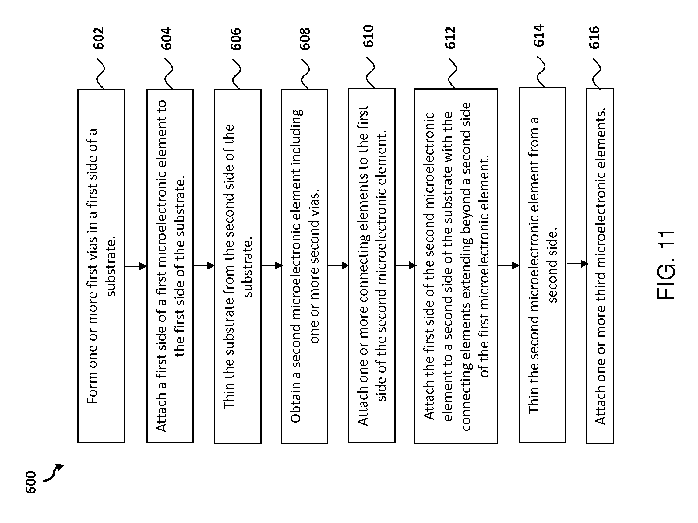
SUMMARY
In some embodiments, as described herein, a method of forming a semiconductor package comprises forming one or more first vias in a first side of a substrate; attaching a first side of a first microelectronic element to the first side of the substrate, the first microelectronic element electrically coupled to at least one of the one or more first vias; obtaining a second microelectronic element including one or more second vias in a first side of the second microelectronic element, with one or more connecting elements each of which has a first end attached to a first side of the second microelectronic element; and attaching a second side of the substrate to the first side of the second microelectronic element, the second microelectronic element electrically coupled to at least one of the one or more first vias. In some embodiments, a second end of each of the one or more connecting elements extends beyond a second side of the first microelectronic element.
In some embodiments, a semiconductor package comprises a substrate comprising one or more first vias extending through the substrate from a first side of the substrate to a second side of the substrate; a first microelectronic element attached to the first side of the substrate and electrically coupled to at least one of the one or more first vias; a second microelectronic element attached to the second side of the substrate and electrically coupled to at least one of the one or more first vias; and one or more connecting elements each having a first end attached to the second microelectronic element and a second end extending beyond the first microelectronic element.
In some embodiments, a semiconductor package comprises a substrate comprising one or more vias extending through the substrate from a first side of the substrate to a second side of the substrate; a first microelectronic element attached to the first side of the substrate and electrically coupled to at least one of the one or more vias; and an encapsulation layer encapsulating the first microelectronic element and the substrate. In some embodiments, the encapsulation layer comprises a carbon material dispersed therein to increase thermal conductivity of the encapsulation layer. In some embodiments, the semiconductor package further comprises a second microelectronic element attached to the second side of the substrate and electrically coupled to at least one of the one or more vias; and one or more connecting elements each having a first end attached to the second microelectronic element and a second end extending beyond the first microelectronic element. In some embodiments, at least one of the one or more connecting elements comprises a carbon material to increase thermal conductivity of the at least one of the one or more connecting elements.
BRIEF DESCRIPTION OF THE DRAWINGS
FIGS. 1-3, and 4A-4B are cross-sectional views of an integrated circuits (IC) assembly fabricated according to some embodiments of the present disclosure.
FIG. 5 is a schematic cross-sectional view of components of an IC assembly according to some embodiments of the present disclosure.
FIG. 6 is cross-sectional view of an IC assembly according to some embodiments of the present disclosure.
FIGS. 7A-7B are cross-sectional views a second-level module according to some embodiments of the present disclosure.
FIGS. 8A-8B are cross-sectional views of fourth-level modules formed by stacking two second-level modules in various embodiments of the present disclosure.
FIG. 9 is a cross-sectional view of an IC assembly formed by stacking various modules according to some embodiments of the present disclosure.
FIG. 10 is a cross-sectional view of an IC packaging structure according to some embodiments of the present disclosure.
FIG. 11 is a flow chart illustrating a method for IC packaging according to some embodiments of the present disclosure.
DESCRIPTION OF SOME EMBODIMENTS
In addition to the foregoing features, other features and advantages will be understood by persons of ordinary skill in the art having benefit of the present description. The following disclosure provides many different embodiments, or examples, for implementing different features of the provided subject matter. Specific examples of components and arrangements are described below to simplify the present disclosure. These are, of course, merely examples and are not intended to be limiting. For example, the formation of a first feature over or on a second feature in the description that follows may include embodiments in which the first and second features are formed in direct contact, and may also include embodiments in which additional features may be formed between the first and second features, such that the first and second features may not be in direct contact.
Further, spatially relative terms, such as "beneath," "below," "lower," "above," "upper" and the like, may be used herein for ease of description to describe one element or feature's relationship to another element(s) or feature(s) as illustrated in the figures. The spatially relative terms are intended to encompass different orientations of the device in use or operation in addition to the orientation depicted in the figures. The apparatus may be otherwise oriented (rotated 90 degrees or at other orientations) and the spatially relative descriptors used herein may likewise be interpreted accordingly.
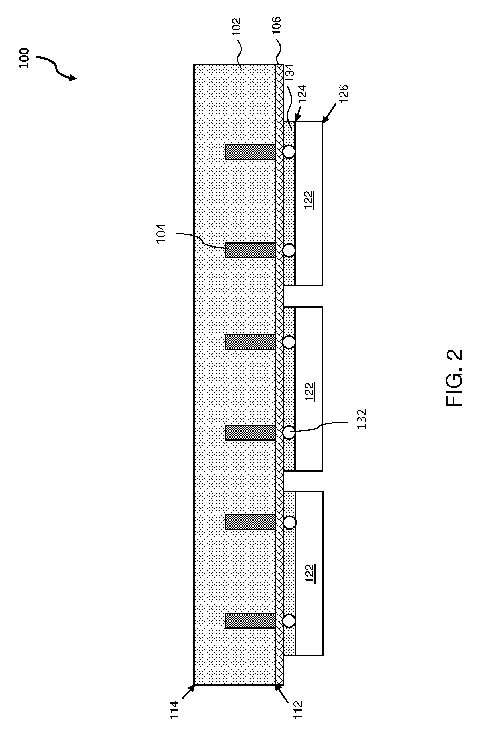
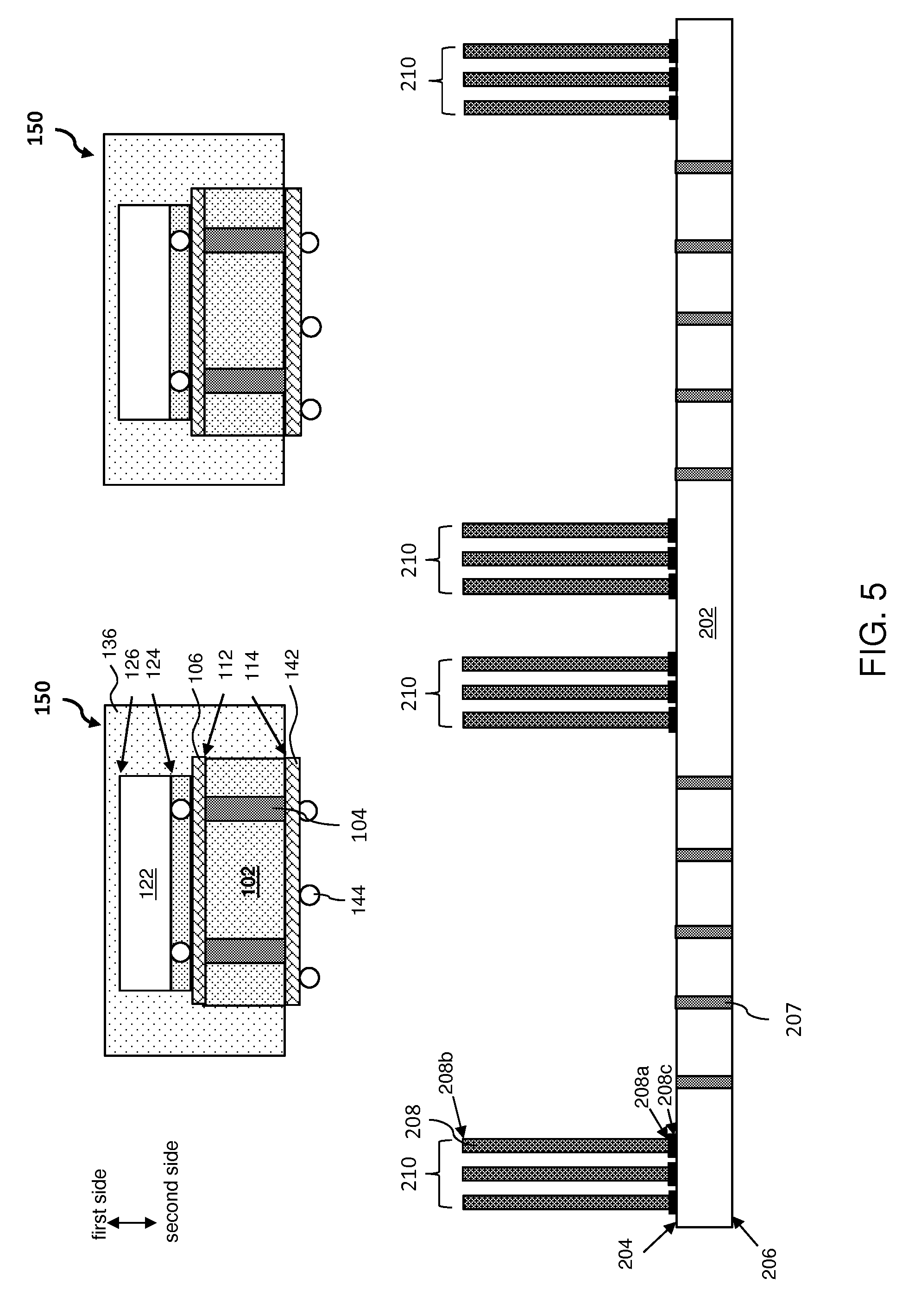
FIGS. 1-3, and 4A-4B are cross-sectional views of an integrated circuit (IC) assembly 100 fabricated according to some embodiments of the present disclosure. Referring to FIG. 1, the IC assembly 100 includes an interposer substrate 102 having a first (top) side 112 and a second (bottom) side 114. In some embodiments, interposers are used as intermediate substrates (e.g., between die or die packages, between printed circuit boards and die, etc.) which are useful for rewiring input/output (I/O) terminals between the back side and the front side of the interposer substrate 102, and/or to improve heat dissipation and mechanical strength, and/or absorb mismatches of coefficients of thermal expansion (CTE) between other components of the system. The interposer substrate 102 may be initially chosen to be sufficiently thick to provide easy handling and adequate heat dissipation in fabrication, and can be thinned later. In some embodiments, the interposer substrate 102 may include a single crystal silicon (Si) wafer with a diameter of about 200 mm or about 300 mm, and a thickness of about 650 micron or more. These materials and dimensions are merely exemplary and not limiting. The interposer substrate 102 may also include other semiconductor materials (e.g., gallium arsenide GaAs), glass, sapphire, metal, or possibly other materials. Other possible materials for the interposer substrate 102 may include NbTaN and LiTaN. In some embodiments, the interposer may also include active circuits, e.g. transistors.
Still referring to FIG. 1, the interposer substrate 102 may include one or more electrically conductive vias 104. The vias 104 may be "blind vias", terminating inside the interposer substrate 102 as shown in the exemplary FIG. 1. Alternatively, one or more vias 104 may penetrate the interposer substrate 102, forming through substrate vias (TSVs). The vias 104 may include, or be made of, copper (Cu), tungsten (W), or any other suitable metal or non-metal conductive materials. In some embodiments, the vias 104 may be formed using a lithography process, an etching process, and a filling/deposition process. The lithography process may include forming a resist layer (not shown) over the first side 112 of the interposer substrate 102 and patterning the resist layer to define the locations of the vias 104. The etching process may then be performed using the patterned resist layer as an etching mask to form one or more holes for vias 104 in the interposer substrate 102. The etching process may include a dry etch such as a reactive ion etching (RIE) process. The vias 104 may include vertical, sloped, or any other shapes. Conductive material may then be deposited into the holes to form the vias 104. Dielectric can be formed between the conductive material and the holes' surfaces if needed for electrical insulation. A barrier layer can be formed between the conductive material and the holes' surfaces if needed for improved adhesion and preventing interdiffusion, as known in the art. The vias can be formed, for example, by electroplating or other techniques.
Still referring to FIG. 1, a first redistribution layer (RDL) 106 is formed on the first (top) side 112 of the interposer substrate 102. In some embodiments, the first RDL 106 includes interconnect lines (not shown) insulated from each other and insulated from interposer substrate 102 by the RDL's dielectric (not shown separately). The RDL provides contact pads (not shown) on top of the interposer. The RDL's interconnect lines interconnect the contact pads and vias 104 in the interposer substrate 102 as desired; an interconnect may connect contact pads to each other and/or to one or more vias 104, or may connect vias 104 to each other. In the various embodiments described herein, the interposer substrate 102 and RDLs (including the first RDL 106 or other RDL layers described below) may also include transistors, resistors, capacitors, and other devices (not shown). It is to be understood that FIG. 1 is merely exemplary and the first RDL 106 may be omitted.
Referring to FIG. 2, the interposer substrate 102 is rotated with the second (bottom) side 114 facing up and the first (top) side 112 facing down. In some embodiments, one or more first microelectronic (ME) elements 122 (e.g. chips (also called die, or possibly other electronic assemblies or packages) are attached to the first side 112 of the interposer substrate 102. For example, the circuitry of ME elements 122 may be coupled to the vias 104. ME elements 122 may include any types of circuits, including possibly memory, logic, control, and/or other types. Each ME element 122 has a first side 124, and a second side 126. As shown in FIG. 2, the first side 124 of each ME element 122 is attached to the first RDL 106 formed over the first side 112 of the interposer 102. In some alternative examples, the first side 124 of at least one ME element 122 is attached directly to the first side 112 of the interposer 102 without using the first RDL 106. In some examples, one or more of the vias 104 may be used to provide electrical connection and/or thermal conduction paths to transfer heat away from the ME elements or from other heat-sensitive components (i.e. a via 104 may have no electrical functionality).
Still referring to FIG. 2, in order to attach the first side 124 of each ME element 122 to the first side 112 of the interposer 102, one or more contact elements 132 (e.g. solder balls) may be formed on the first RDL 106. The contact elements 132 may also include conductive or anisotropic adhesive, or other types of connections. The contact elements 132 are a schematic representation of attachments to other structures as described below, and in some embodiments the contact elements 132 are not separate elements (e.g. if the attachment is by thermocompression). If contact elements 132 are separate elements, they may be attached to one or more contact pads (not shown) provided by the first RDL 106. The contact elements 132 may include metals such as tin (Sn), indium (In), gold (Au), or metal alloys. There examples are exemplary embodiments and not limiting. The contact elements 132 may have any other suitable form, such as elongated connectors, and/or a series of stacked conductive masses.
Still referring to FIG. 2, an underfill 134 may be formed between the first RDL 106 and the first side 124 of each ME element 122. In some examples, the underfill 134 may be formed prior to or after the attachment of the ME elements 122. The underfill 134 may include an epoxy with silica or other particles, or other suitable polymeric materials. The underfill 134 may protect the ME elements and/or electrical connections (e.g., contact elements 132) from moisture and other contaminants, ultraviolet light, alpha particles, and possibly other harmful elements. The underfill 134 can also strengthen the attachment between RDL and the ME elements. In some embodiments, the underfill may 134 may also help to conduct heat away from the ME elements 122.
Referring to FIG. 3, in some embodiments, an encapsulation 136 is formed over the second sides 126 of ME elements 122 by molding or other techniques. The encapsulation 136 includes any suitable materials, such as epoxy with silica or other particles, or other suitable polymeric materials. In some embodiments, the encapsulation 136 includes carbon materials, such as graphite, dispersed in the encapsulation 136 to increase thermal conductivity of the encapsulation 136.
Optionally, carrier wafer 138 can be attached to a surface 137 of encapsulation 136. The carrier wafer 138 can be used as a support wafer during processing and can be removed upon process completion. For example, when the IC assembly 100 has sufficient mechanical strength to withstand handling, the carrier wafer 138 may be unnecessary.
As shown in FIG. 3, if one or more of the original vias 104 are "blind vias" as shown in FIG. 1, the interposer substrate 102 is then thinned from the second side 114 to expose the buried ends of the vias 104 and thus turn the blind vias into TSVs. The back-side thinning process 139 may include reactive ion etching (RIE) and/or other dry etching processes, and/or wet etching, and/or grinding and/or lapping and/or chemical mechanical polishing (CMP) and/or other processes. A planar surface may be formed by the TSVs 104 and the interposer substrate 102 after the thinning process 139 as shown in FIG. 3. In other embodiments, TSVs 104 protrude out of the interposer. See e.g. U.S. Pat. No. 6,639,303 issued Oct. 28, 2003 to Siniaguine and incorporated herein by reference.
In an alternative embodiment, vias 104 are not provided at the stage of FIG. 1 but are formed after thinning the interposer substrate to obtain the structure of FIG. 3. In other embodiments, the holes for vias 104 are formed at the stage of FIG. 1, but the holes are filled with conductive material at the stage of FIG. 3. The dielectric or other layers in vias 104 can be formed partly at the stage of FIG. 1 and partly at the stage of FIG. 3.
Referring to FIG. 4A, a second RDL 142 is formed on the second side 114 of the interposer 102. The RDL 142 provides contact pads (not shown) on side 114 of the interposer. The RDL's interconnect lines interconnect the contact pads and vias 104 in the interposer substrate 102 as desired; an interconnect may connect contact pads to each other and/or to one or more vias 104, or may connect vias 104 to each other. In some embodiments, the interposer substrate 102, the RDL 106, and the RDL 142 may include transistors, resistors, capacitors, and/or other devices (not shown). The components and methods used to form the RDL 142 may be substantially similar to those for the RDL 106. In some embodiments, the RDL 142 is omitted.
One or more contact elements 144 are shown on the second RDL 142. These may be separate elements, such as solder balls, or just a schematic representation indicating possible attachment to other structures. If they are separate elements, they may be attached to one or more contact pads (not shown) provided by the second RDL 142. The contact elements 144 may include a bond metal such as tin (Sn), indium (In), gold (Au), metal alloys, or a curable material. It is to be understood that the contact elements 144 such as solder balls shown in FIG. 4A are merely exemplary embodiments and are not intended to be limiting. The contact elements 144 may have any other suitable form, such as elongated connectors (e.g. copper posts), and/or a series of stacked conductive masses. The contact elements 144 may be substantially similar to the contact elements 132 shown in FIG. 2.
Still referring to FIG. 4A, the IC assembly 100 is then diced along the dice lines 146 to form a plurality of first-level modules 150. The carrier wafer 138 may be removed before or after dicing. As shown in FIG. 4B, each first-level module 150 includes an ME element 122 stacked on the interposer 102, and the interposer 102 includes one or more TSVs 104. (Of note, we use numeral 102 to refer both to the interposer substrate 102 and to the entire interposer, i.e. the substrate with the RDLs.) In some embodiments, the TSVs 104 are coupled to the ME element 122 to provide electrical connection between the ME element 122 and the other components in the IC packaging, and/or thermal conduction to transfer heat away from the ME element 122.
FIGS. 5-6 are cross-sectional views of an IC assembly 200 according to some embodiments of the present disclosure. In the present embodiment, the IC assembly 200 includes multiple ME elements, i.e. two ME elements stacked together. The IC assembly 200 may be used to fabricate one or more second-level modules 250 (FIGS. 7A, 7B) as discussed below. The IC assembly 200 and the second-level module 250 are exemplary and not limiting. The IC assembly may include any suitable numbers of ME elements stacked together.
Referring to FIG. 5, a second ME element 202 may include a wafer or a chip ("die") including a semiconductor integrated circuit, which could include memory, logic or control circuitry (e.g. a computer processor), or other types of circuits. The second ME element 202 may or may not be substantially similar to the ME element 122, e.g. the two ME elements may perform the same or different functions. The second ME element 202 may include a substrate different from the substrate of the first ME element 122.
Still referring to FIG. 5, the ME element 202 has a first (top) side 204, and a second (bottom) side 206. The ME element 202 includes one or more electrically conductive vias 207. In some embodiments as shown in FIG. 5, the vias 207 are through substrate vias (TSVs) 207 extending from the top side 204 through the ME element 202 to the bottom side 206. The TSVs 207 may be made by the same processes as discussed above for TSVs 104 in the interposer 102. In some alternative embodiments, the vias 207 are "blind vias" extending from side 204 and terminating inside the ME element 202.
Alternatively, the ME element 202 may include a substrate (e.g. semiconductor, glass, and/or other materials) with an RDL (not shown) on top and/or bottom; the vias 207 are made in the substrate as blind vias or TSVs 207 passing through the substrate; vias 207 are connected to top and/or bottom contact pads of ME element 202, and possibly to each other, by the RDL interconnects as needed.
As shown in FIG. 5, one or more connecting elements 208 are formed on the first side 204 of the second ME element 202. In some embodiments, each connecting element 208 includes a first end (e.g., base) 208a attached to ME element 202, and includes the opposite second end (e.g., tip) 208b. Connecting elements 208 may or may not be vertical. The first end 208a may be widened to provide a pad 208c on the first side 204 of the second ME element 202. The pad 208c may be made of copper, nickel, aluminum, tin, palladium, other suitable conductive material, or combinations thereof. In some embodiments, the connecting element 208 may include conductive materials such as copper, nickel, aluminum, tin, palladium, or other suitable conductive materials to provide electrical conduction between the ME element 202 and the other components. In some embodiments, the connecting element 208 may include carbon materials, such as graphite, to increase the thermal conductivity and to transfer heat away from the second ME element 202. In some embodiments, the connecting elements 208 may be arranged to form connecting arrays 210. The connecting arrays 210 may be formed at the peripheral areas to surround the first-level modules 150 to be attached to the second ME element 202 as discussed below. Connecting elements 208 can be wires bonded to ME element 202 as described, for example, in Invensas.TM. High Performance BVA PoP package for Mobile Systems, May 2013 by Invensas Corporation of San Jose, Calif., and is incorporated herein by reference. See also U.S. Pat. No. 8,618,659 issued Dec. 31, 2013 to Sato et al. and incorporated herein by reference.
Referring to FIG. 6, one or more first-level modules 150 are attached to the first side 204 of the second ME element 202. In some embodiments, the vias 207 of the second ME element 202 may be coupled to the vias 104 of the interposer 102. In some examples as shown in FIG. 6, the second RDL 142 is formed over the second side 114 of the interposer substrate 102 and electrically coupled to the vias 207 of the second ME element 202 and the interposer 102. The RDL 142 is attached to contact elements 144 placed on the second ME element 202. In some alternative examples, the interposer 102 may be directly attached to the second ME element 202 without using the second RDL 142. Prior to or after attaching the first-level module 150 to the second ME element 202, an underfill 212 may be formed between the second RDL 142 and the second ME element 202. The underfill 212 can be made of the same materials, and perform the same function, as described above for underfill 134.
In some embodiments as shown in FIG. 6, connecting arrays 210 are formed at the peripheral areas to partly or completely surround the first-level modules 150 attached to the second ME element 202. In some embodiments, the conducting elements 208 may include pads, conductive masses (e.g., solder balls), Bond Via Array.TM. (BVA) technology from Invensas Corporation of San Jose, Calif., or any other suitable elements.
Still referring to FIG. 6, an encapsulation 214 is formed over the first side 204 of the second ME element 202, possibly by molding, possibly using the same techniques and materials and performing the same functions as described above for encapsulation 136. In some embodiments, the second ends 208b of the connecting elements 208 protrude out of a surface 217 of the encapsulation 214. The protruding ends 208b may extend beyond the ME element 122 as shown in FIG. 6. The protruding ends 208b may be used to connect other components in the IC package. The protruding ends 208b may be available for electrical conduction and/or thermal conduction.
In some embodiments, a carrier wafer (not shown) may be attached to the bottom of ME element 206 to provide support during processing, and the carrier wafer may be removed upon process completion. The carrier wafer may be optional.
Still referring to FIG. 6, the IC assembly 200 is then diced along the dice lines 216 to form the one or more second-level modules 250. Each the second-level module 250 includes an ME element 122 stacked on the first side 112 of the interposer 102, and the second ME element 202 stacked on the second side 114 of the interposer 102. The interposer 102 includes one or more TSVs 104. The second ME element 202 may also include one or more TSVs 207. In some embodiments, at least one of the TSVs 104, the TSVs 207, and the connecting elements 208/connecting arrays 210 may provide electrical connection and/or thermal conduction in the second-level module 250.
FIGS. 7A-7B are cross-sectional views of a second-level module 250 according to some embodiments of the present disclosure. FIGS. 7A and 7B show similar structures except that FIG. 7B does not have RDLs on the interposer. Second-level module 250 includes the interposer 102, the ME element 122 disposed on the first side 112 of the interposer 102, and the second ME element 202 disposed on the second side 114 of the interposer 102. Each of the interposer 102, the ME element 122, and the second ME element 202 may include one or more TSVs (e.g., TSVs 104, TSVs 256, or TSVs 207). The connecting arrays 210 (e.g., BVAs) may also be formed on the second ME element for connecting the second ME element to other components (not shown). As shown in FIGS. 7A-7B, the connecting arrays 210 include protruding ends which extend beyond the ME element 122. The TSVs and the connecting arrays 210 may be used for electrical conduction and/or thermal conduction. In some embodiments, RDL (e.g., RDL 106 and/or RDL 142) may be formed on the first side 112 and/or the second side 114 as shown in FIG. 7A. In some embodiments, one or more contact elements (e.g., solder balls) and underfill may be used for attaching the ME element 122 and/or the second ME element 202 to the interposer 102 as shown in FIG. 7A. Molding or other process may also be performed to encapsulate the second-level module 250 into additional encapsulant (not shown).
FIGS. 8A-8B are cross-sectional views of exemplary fourth-level modules 300 each of which is a stack of two second-level modules 250 (i.e. 250-1 and 250-2). In FIG. 8A, the modules 250-1, 250-2 are attached to each other bottom-to-bottom (i.e. second side to second side): the second sides 206 of the second ME element 202 of second-level modules 250-1 and 250-2 may be attached to each other using connections 302. Each connection 302 may include one or more connecting elements (e.g., solder balls) or other types of connections attached to one or more pads in the second-level modules. (Connections 302 can also be simply schematic representations and not separate physical elements if, say, thermocompression is used.)
In FIG. 8B, the modules 250-1, 250-2 are attached to each other bottom-to-top: the second (bottom) side 206 of the second ME element 202 of module 250-1 is attached to the top of module 250-2, i.e. to the second side 126 of the first ME element 122 of module 250-2. The attachment is by connections 304 which can be as connections 302.
FIG. 9 is an example of such assembly 400, showing a cross-sectional view. The IC assembly 400 may be formed by sequentially stacking a number i of modules from the first level to the i-th level using the process substantially similar to the process discussed in FIGS. 1-6, 7A-7B, and 8A-8B. For example, an (i-2)-level module 402 (generally representing for example one or more first-level modules 150 of FIG. 5; second-level modules 250 of FIG. 7A or 7B; or a stack such as of two second-level modules 250-1 and 250-2 of FIG. 8A or 8B) may be attached to a (i-1)-th ME element 404 to form a (i-1)-level module 406. The (i-2)-level module 402 may include a number i-2 of ME elements attached to each other and possibly separated by one or more interposers. Each ME element and each interposer included in the (i-2)-level module 402 may include one or more TSVs. The (i-2)-level module 402 may be attached to the (i-1)-the ME element 404 by contacts 420 (e.g., solder balls, BVAs, or TSVs). The (i-1)-the ME element 404 may include TSVs 422 or BVAs 422. The contacts 420 may be coupled to the TSVs 422 or BVAs 422 of the (i-1)-the ME element 404. One or more connecting arrays 405 may be formed on the (i-1)-th ME element 404, and the (i-2)-level module 402 may then be attached to and encapsulated (e.g. molded) together with the (i-1)-th ME element 404 to form the (i-1)-level module 406.
Still referring to FIG. 9, the connecting arrays 410 may be formed on an i-th ME element 408, and the formation of the connecting arrays 410 may be substantially similar to that of the connecting arrays 210 as discussed in FIG. 6. The (i-1)-level modules 406 may be attached to and molded with the i-th ME element 408 to form the IC assembly 400, which includes one or more i-level modules 450. As shown in FIG. 9, the (i-2)-level module 402 may be attached to the i-th ME element 408 by contacts 424 (e.g., solder balls, BVAs, or TSVs). The i-th ME element 408 may include TSVs 426 or BVAs 426. The contact 424 may be coupled to the TSVs 426 or BVAs 426 of the i-th ME element 408. The IC assembly 400 may be diced along the dice lines 412 to form the one or more i-level modules 450.
As shown in FIG. 9, the i-level module 450 may be obtained by sequential stacking of other modules along a Z direction, and the interposer and/or the ME element of each level may be disposed along an X-Y plane. The ME elements and interposers of the i-level module 450 may include one or more TSVs (e.g., TSVs 422 and/or TSVs 426) for providing electrical and/or thermal conduction along the Z direction. The connecting arrays (e.g., connecting arrays 405 or connecting arrays 410) may also provide electrical and/or thermal conduction along the Z direction. In some embodiments, one or more interposer included in the i-level module 450 may include one or more carbon materials, such as graphite, for providing improved thermal conductivity in the X-Y plane.
FIG. 10 is a cross-sectional view of an IC packaging structure 500 according to some embodiments of the present disclosure. The IC packaging structure 500 may include a hybrid stacking assembly. The IC packaging structure 500 may include an ME element 502, and the ME element 502 may include a chip (or a "die") or wafer having semiconductor integrated circuits that perform any type of functions, e.g. memory, logic, control, and/or other types. The ME element 502 may include a substrate with one or more vias 504. Vias 504 may be either blind vias or through substrate vias (TSVs) fabricated as discussed with regard to TSVs 104 in interposer substrate 102. The vias 504 may provide electrical connection between the circuits above, below, or within the ME element 502. The vias 504 may also provide thermal conduction to transfer heat away from such circuits.
Referring to FIG. 10, one or more connecting arrays 506 are formed on the ME element 502. The formation of the connecting arrays 506 may be substantially similar to that of the connecting arrays 210 as discussed in FIG. 6, for example, the connecting arrays 506 may be BVAs. The BVAs 506 may provide electrical connection between the ME element 502 and one or more other components in IC packaging structure 500. The BVAs 506 may also provide heat conduction away from the ME 502.
Various IC components are attached to the ME element 502 from above or below to form IC packaging structure 500. Thus, first level module 508 or some other type of module may be attached and electrically coupled to some BVAs 506. In some examples, an i-th level module 510 may be attached to the ME element 502, wherein i equals to 1, 2 . . . , or n. The i-th level module 510 may include a number i of ME elements stacked with one or more interposers as discussed with regard to the i-level module 450 in FIG. 9. In some examples, a single chip 512 may also be included in the IC packaging structure 500. The single chip 512 may include a semiconductor integrated circuit configured to perform one or more of a memory function, a logic function, a control function, or other processing function. The single chip 512 may be stacked on an i-level module 510 as shown in FIG. 10. The single chip 512 may also be stacked on any other component of the IC packaging structure 500. The attaching and stacking processes used to fabricate the IC packaging structure 500 may include any suitable packaging technologies. For example, solder balls, contact pads, underfills, and encapsulations may be used to connect and mold various components in the IC packaging structure 500. One or more RDLs may also be included in the IC packaging structure 500.
In a three-dimensional system in FIG. 10, the IC packaging structure 500 may be stacked along a Z direction, and the interposer and/or the ME element of each level may be disposed along an X-Y plane. The TSVs formed along the Z direction in the one or more ME elements and/or interposers may provide electrical conduction and/or thermal conduction along the Z direction in the IC packaging structure 500. The connecting arrays may also provide electrical conduction and/or thermal conduction along the Z direction in the IC packaging structure 500. In some embodiments, one or more interposers may include one or more carbon materials, such as graphite, for providing improved thermal conductivity in the X-Y plane in the IC packaging structure 500.
FIG. 11 is a flow chart illustrating a method 600 for IC packaging according to some embodiments of the present disclosure. It should be understood that method 600 in the flow chart FIG. 11 is merely exemplary and not meant to be limiting. Any additional processes may be provided before, during, and after the method 600.
The method 600 starts from a process 602 by forming one or more vias (e.g., the vias 104) in a first side (e.g., the first side 112) of a substrate (e.g., the interposer 102). The vias may be "blind vias" terminating inside the substrate. Alternatively, the vias may be through substrate vias (TSVs) extending through the interposer substrate from the first side to the second side (e.g., the second side 114) of the substrate. The vias may be formed by lithography and etching or laser drilling to form holes for the vias, followed by conductor filling of the holes, and back-side thinning of the substrate to reveal the conductor.
The method 600 proceeds to a process 604 of attaching a first side (e.g., the first side 124) of a first microelectronic element (ME) (e.g., the ME element 122) to the first side of the substrate. The vias formed in the substrate may be coupled to the first ME element. One or more contact elements, such as solder balls, may be used to connect the substrate and the first ME element. An underfill can be provided between the substrate and the first ME element, and an encapsulation may be formed by molding to encapsulate the first ME element and possibly the substrate.
The method 600 proceeds to an optional process 606 which thins the substrate from the second side of the substrate. In some embodiments, the buried ends of the "blind vias" may be exposed by the thinning process to form TSVs. The back-side thinning may include wet and/or dry etching (e.g., reactive ion etching RIE), and/or mechanical grinding or lapping or milling and/or chemical mechanical polishing (CMP).
The method 600 proceeds to a process 608 by obtaining a second ME element (e.g., the ME element 202), and the second ME element may include one or more vias (e.g., the vias 207). The vias in the second ME element may include TSVs. Alternatively, the vias in the second ME element may include "blind vias".
The method 600 proceeds to a process 610 by attaching one or more connecting elements (e.g., connecting elements 208/connecting arrays 210) to a first side (e.g., the first side 204) of the second ME element. In some embodiments, each connecting element extends perpendicularly to the second ME element, between its first end (e.g., base) and a second end (e.g., tip). In some embodiments, the connecting element may include conductive materials to provide electrical conduction between the second ME element and the other components. In some embodiments, the connecting element may include carbon materials, such as graphite, for increasing thermal conductivity to transfer heat away from the second ME element. In some embodiments, the one or more connecting elements may be arranged to form connecting arrays. The connecting arrays may be formed at the peripheral areas to surround the first-level modules to be attached on the second ME element.
The method 600 proceeds to a process 612 by attaching the first side of the second ME element to the second side of the substrate. The connecting elements/connecting arrays may extend beyond a second side (e.g., the second side 126) of the first ME element.
The method 600 proceeds to an optional process 614 by performing a thinning process to the second ME element from a second side (e.g., the second side 206) of the second ME element. In some embodiments, the buried ends of the "blind vias" may be exposed after the thinning process to form TSVs in the second ME element. The back-side thinning process may include a wet etching process, a dry etching process (e.g., reactive ion etching RIE), and/or a chemical mechanical polishing (CMP) process.
The method 600 proceeds to a process 616 of attaching one or more third ME elements to the IC connecting elements. The one or more third ME elements may include a single chip, a first level module, and/or a multiple level module stacked together using any suitable packaging technologies. For example, the one or more third ME elements may be attached to the IC packaging structure using one or more contact pads (possibly with solder balls), and underfill.
The foregoing outlines features of several embodiments so that those skilled in the art may better understand the aspects of the present disclosure. Those skilled in the art should appreciate that they may readily use the present disclosure as a basis for designing or modifying other processes and structures for carrying out the same purposes and/or achieving the same advantages of the embodiments introduced herein. Those skilled in the art should also realize that such equivalent constructions do not depart from the spirit and scope of the present disclosure, and that they may make various changes, substitutions, and alterations herein without departing from the spirit and scope of the present disclosure.
* * * * *
References
D00000
D00001
D00002
D00003
D00004
D00005
D00006
D00007
D00008
D00009
D00010
D00011
XML
uspto.report is an independent third-party trademark research tool that is not affiliated, endorsed, or sponsored by the United States Patent and Trademark Office (USPTO) or any other governmental organization. The information provided by uspto.report is based on publicly available data at the time of writing and is intended for informational purposes only.
While we strive to provide accurate and up-to-date information, we do not guarantee the accuracy, completeness, reliability, or suitability of the information displayed on this site. The use of this site is at your own risk. Any reliance you place on such information is therefore strictly at your own risk.
All official trademark data, including owner information, should be verified by visiting the official USPTO website at www.uspto.gov. This site is not intended to replace professional legal advice and should not be used as a substitute for consulting with a legal professional who is knowledgeable about trademark law.