Methods, Apparatus, And System For A Semiconductor Device Comprising Gates With Short Heights
Shu; Jiehui ; et al.
U.S. patent application number 16/525601 was filed with the patent office on 2019-11-21 for methods, apparatus, and system for a semiconductor device comprising gates with short heights. This patent application is currently assigned to GLOBALFOUNDRIES, INC.. The applicant listed for this patent is GLOBALFOUNDRIES, INC.. Invention is credited to Garo Jacques Derderian, Haigou Huang, Jinping Liu, Jiehui Shu, Hui Zang, John Zhang.
| Application Number | 20190355615 16/525601 |
| Document ID | / |
| Family ID | 67909187 |
| Filed Date | 2019-11-21 |


View All Diagrams
| United States Patent Application | 20190355615 |
| Kind Code | A1 |
| Shu; Jiehui ; et al. | November 21, 2019 |
METHODS, APPARATUS, AND SYSTEM FOR A SEMICONDUCTOR DEVICE COMPRISING GATES WITH SHORT HEIGHTS
Abstract
At least one method, apparatus and system providing semiconductor devices with relatively short gate heights but without a relatively high risk of contact-to-gate shorts. In embodiments, the method, apparatus, and system may provide contact formation by way of self-aligned contact processes.
| Inventors: | Shu; Jiehui; (Clifton Park, NY) ; Derderian; Garo Jacques; (Saratoga Springs, NY) ; Zang; Hui; (Guilderland, NY) ; Zhang; John; (Altamont, NY) ; Huang; Haigou; (Rexford, NY) ; Liu; Jinping; (Ballston Lake, NY) | ||||||||||
| Applicant: |
|
||||||||||
|---|---|---|---|---|---|---|---|---|---|---|---|
| Assignee: | GLOBALFOUNDRIES, INC. Grand Cayman KY |
||||||||||
| Family ID: | 67909187 | ||||||||||
| Appl. No.: | 16/525601 | ||||||||||
| Filed: | July 30, 2019 |
Related U.S. Patent Documents
| Application Number | Filing Date | Patent Number | ||
|---|---|---|---|---|
| 15976326 | May 10, 2018 | 10418272 | ||
| 16525601 | ||||
| Current U.S. Class: | 1/1 |
| Current CPC Class: | H01L 27/0924 20130101; H01L 21/76224 20130101; H01L 29/66795 20130101; H01L 21/0228 20130101; H01L 21/823431 20130101; H01L 21/823821 20130101; H01L 29/785 20130101; H01L 27/0886 20130101; H01L 21/02282 20130101; H01L 21/02167 20130101 |
| International Class: | H01L 21/762 20060101 H01L021/762; H01L 27/088 20060101 H01L027/088; H01L 21/8234 20060101 H01L021/8234; H01L 21/8238 20060101 H01L021/8238; H01L 27/092 20060101 H01L027/092; H01L 21/02 20060101 H01L021/02; H01L 29/78 20060101 H01L029/78; H01L 29/66 20060101 H01L029/66 |
Claims
1.-7. (Canceled)
8. A semiconductor device, comprising: a semiconductor substrate; an active area disposed on the semiconductor substrate; a shallow trench isolation (STI) disposed in the silicon substrate adjacent to the active area; a gate disposed over the active area and the STI; a first spacer disposed on one gate sidewall and a second spacer disposed on another gate sidewall, wherein a top of the gate is below a top of the first spacer and a top of the second spacer; and a silicon nitride cap disposed on the gate, on the top of the first spacer, and on the top of the second spacer.
9. The semiconductor device of claim 8, further comprising: a source disposed over the active area and the STI and adjacent to a first side of the gate; and a drain disposed over the active area and the STI and adjacent to a second side of the gate.
10. The semiconductor device of claim 9, further comprising: a source contact disposed over the source over the active area; a drain contact disposed over the drain over the active area; and a gate contact disposed over the gate over the STI.
11. The semiconductor device of claim 10, further comprising: a dielectric material disposed over the source over the STI and over the drain over the STI.
12. The semiconductor device of claim 8, wherein the silicon nitride cap has a height of about 10 nm.
13. The semiconductor device of claim 12, wherein the gate has a height above the semiconductor substrate of less than about 80 nm.
14. A system, comprising: a semiconductor device processing system to manufacture a semiconductor device; and a processing controller operatively coupled to the semiconductor device processing system, the processing controller configured to control an operation of the semiconductor device processing system; wherein the semiconductor device processing system is adapted to: form a gate over at least one active area disposed on a semiconductor substrate; form a first spacer disposed on one gate sidewall and a second spacer disposed on another gate sidewall; form a dielectric material adjacent the first spacer and adjacent the second spacer; recess the gate to below a top of the first spacer and a top of the second spacer; form a silicon nitride liner on a top of the recessed gate; grow a silicon nitride cap selectively on the silicon nitride liner and at least on a top of the first spacer and a top of the second spacer; and form contacts to the gate and the active area, wherein contact formation is self-aligned by the silicon nitride cap.
15. The system of claim 14, wherein the semiconductor device processing system is adapted to form the silicon nitride liner by: depositing by atomic layer deposition (ALD) silicon nitride on a top of the recessed gate, on an exposed sidewall portion and a top of the first spacer, on an exposed sidewall portion and a top of the second spacer, and on a top of the dielectric material; coating the silicon nitride with a spin-on carbon polymer; recessing the spin-on carbon polymer to below the top of the first spacer and the top of the second spacer, to yield recessed spin-on carbon polymer; removing the silicon nitride above the recessed spin-on carbon polymer, to yield the silicon nitride liner; and removing the recessed spin-on carbon polymer.
16. The system of claim 14, wherein the semiconductor device processing system is adapted to grow the silicon nitride cap by treating the dielectric material to prevent silicon nitride growth on the dielectric material.
17. The system of claim 14, wherein the semiconductor device processing system is adapted to further grow the silicon nitride cap over a portion of the dielectric material.
18. The system of claim 14, wherein the semiconductor device processing system is adapted to extend the dielectric material to the same height as the silicon nitride cap.
19. The system of claim 14, wherein the semiconductor device processing system is adapted to form the contact to the gate at a position disposed laterally away from the active area.
20. The system of claim 14, wherein the semiconductor device processing system is adapted to form silicon oxide as the dielectric material.
21. A semiconductor device, comprising: a semiconductor substrate; an active area disposed on the semiconductor substrate; a shallow trench isolation (STI) disposed in the silicon substrate adjacent to the active area; a gate disposed over the active area and the STI; a first spacer disposed on one gate sidewall and a second spacer disposed on another gate sidewall, wherein a top of the gate is below a top of the first spacer and a top of the second spacer; a source disposed over the active area and the STI and adjacent to a first side of the gate; and a drain disposed over the active area and the STI and adjacent to a second side of the gate; a dielectric material disposed over the source over the STI and over the drain over the STI; and a silicon nitride cap disposed on the gate, on the top of the first spacer, on the top of the second spacer, on a portion of a top of dielectric material disposed over the source, and on a portion of a top of dielectric material disposed over the drain.
22. The semiconductor device of claim 21, further comprising: a source contact disposed over the source over the active area; a drain contact disposed over the drain over the active area; and a gate contact disposed over the gate over the STI.
23. The semiconductor device of claim 21, wherein the silicon nitride cap has a height of about 10 nm.
24. The semiconductor device of claim 21, wherein the gate has a height above the semiconductor substrate of less than about 80 nm.
Description
BACKGROUND OF THE INVENTION
Field of the Invention
[0001] Generally, the present disclosure relates to the manufacture of sophisticated semiconductor devices, and more specifically, to semiconductor devices having short gate heights.
Description of the Related Art
[0002] The fabrication of advanced integrated circuits, such as CPU's, storage devices, ASIC's (application specific integrated circuits) and the like, requires the formation of a large number of circuit elements in a given chip area according to a specified circuit layout, wherein so-called metal oxide field effect transistors (MOSFETs or FETs) represent one important type of circuit element that substantially determines performance of the integrated circuits. A FET is a device that typically includes a source region, a drain region, a channel region that is positioned between the source region and the drain region, and a gate electrode positioned above the channel region.
[0003] In contrast to a planar FET, which has a planar structure, there are so-called 3D devices, such as an illustrative finFET device, which is a 3-dimensional structure. More specifically, in a finFET, a generally vertically positioned, fin-shaped active area is formed and a gate electrode encloses both of the sides and the upper surface of the fin-shaped active area to form a trigate structure so as to use a channel having a 3-dimensional structure instead of a planar structure. In some cases, an insulating cap layer, e.g., silicon nitride, is positioned at the top of the fin and the finFET device only has a dual-gate structure.
[0004] Using one of various techniques, a plurality of fins is formed on a substrate and a gate, a source, and a drain are formed above the fins. The gate is formed between the source and drain regions.
[0005] In the continuing effort to increase transistor density in semiconductor devices, designers have attempted to reduce the widths of the fins, gate, sources, and drains. However, finding optimal gate heights has proven challenging. As gate widths are reduced, the likelihood of physical collapse of a gate increases. Hence, in the interest of reducing the likelihood of gate collapse, some designers have considered short gates. However, the shorter a gate, the greater the risk that processing errors may allow short circuiting between the gates and contacts to the gates, sources, and/or drains.
[0006] The present disclosure may address and/or at least reduce one or more of the problems identified above.
SUMMARY OF THE INVENTION
[0007] The following presents a simplified summary of the invention in order to provide a basic understanding of some aspects of the invention. This summary is not an exhaustive overview of the invention. It is not intended to identify key or critical elements of the invention or to delineate the scope of the invention. Its sole purpose is to present some concepts in a simplified form as a prelude to the more detailed description that is discussed later.
[0008] Generally, the present disclosure is directed to various methods, apparatus and system for providing relatively short gate heights without a relatively high risk of contact-to-gate shorts and/or providing contact formation by way of self-aligned contact processes.
[0009] In one embodiment, the present disclosure relates to a method comprising forming a gate over at least one fin disposed on a semiconductor substrate; forming a first spacer disposed on one gate sidewall and a second spacer disposed on another gate sidewall; forming a dielectric material adjacent the first spacer and adjacent the second spacer; recessing the gate to below a top of the first spacer and a top of the second spacer; forming a silicon nitride liner on a top of the recessed gate; growing a silicon nitride cap selectively on the silicon nitride liner and at least on a top of the first spacer and a top of the second spacer; and forming contacts to the gate and the fin, wherein contact formation is self-aligned by the silicon nitride cap.
[0010] In one embodiment, the present disclosure relates to a semiconductor device, comprising a semiconductor substrate; a fin disposed on the semiconductor substrate; a shallow trench isolation (STI) disposed in the silicon substrate adjacent to the fin; a gate disposed over the fin and the STI; a first spacer disposed on one gate sidewall and a second spacer disposed on another gate sidewall, wherein a top of the gate is below a top of the first spacer and a top of the second spacer; and a silicon nitride cap disposed on the gate, on the top of the first spacer, and on the top of the second spacer.
[0011] In one embodiment, the present disclosure relates to a system comprising a semiconductor device processing system to manufacture a semiconductor device comprising at least one fin field effect transistor (finFET); and a processing controller operatively coupled to the semiconductor device processing system, the processing controller configured to control an operation of the semiconductor device processing system; wherein the semiconductor device processing system is adapted to implement a method referred to above.
BRIEF DESCRIPTION OF THE DRAWINGS
[0012] The disclosure may be understood by reference to the following description taken in conjunction with the accompanying drawings, in which like reference numerals identify like elements, and in which:
[0013] FIG. 1 illustrates a stylized, simplified plan view of a semiconductor device 100, with an X1-cut line and an X2-cut line indicated, in accordance with embodiments herein;
[0014] FIG. 2 illustrates a stylized depiction of an X1-cut cross-sectional view of the semiconductor device 100 of FIG. 1 after a gate formation process, in accordance with embodiments herein;
[0015] FIG. 3 illustrates a stylized depiction of an X2-cut cross-sectional view of the semiconductor device 100 of FIG. 1 after the gate formation process, in accordance with embodiments herein;
[0016] FIG. 4 illustrates a stylized depiction of an X1-cut cross-sectional view of the semiconductor device 100 of FIGS. 2-3 after a gate recess process, in accordance with embodiments herein;
[0017] FIG. 5 illustrates a stylized depiction of an X2-cut cross-sectional view of the semiconductor device 100 of FIGS. 2-3 after the gate recess process, in accordance with embodiments herein;
[0018] FIG. 6 illustrates a stylized depiction of an X1-cut cross-sectional view of the semiconductor device 100 of FIGS. 4-5 after a silicon nitride deposition process, in accordance with embodiments herein;
[0019] FIG. 7 illustrates a stylized depiction of an X2-cut cross-sectional view of the semiconductor device 100 of FIGS. 4-5 after the silicon nitride deposition process, in accordance with embodiments herein;
[0020] FIG. 8 illustrates a stylized depiction of an X1-cut cross-sectional view of the semiconductor device 100 of FIGS. 6-7 after a spin-on carbon polymer deposition process, in accordance with embodiments herein;
[0021] FIG. 9 illustrates a stylized depiction of an X2-cut cross-sectional view of the semiconductor device 100 of FIGS. 6-7 after the spin-on carbon polymer deposition process, in accordance with embodiments herein;
[0022] FIG. 10 illustrates a stylized depiction of an X1-cut cross-sectional view of the semiconductor device 100 of FIGS. 8-9 after a spin-on carbon polymer recession process, in accordance with embodiments herein;
[0023] FIG. 11 illustrates a stylized depiction of an X2-cut cross-sectional view of the semiconductor device 100 of FIGS. 8-9 after the spin-on carbon polymer recession process, in accordance with embodiments herein;
[0024] FIG. 12 illustrates a stylized depiction of an X1-cut cross-sectional view of the semiconductor device 100 of FIGS. 10-11 after a silicon nitride recession and a spin-on carbon polymer removal process, in accordance with embodiments herein;
[0025] FIG. 13 illustrates a stylized depiction of an X2-cut cross-sectional view of the semiconductor device 100 of FIGS. 10-11 after the silicon nitride recession and a spin-on carbon polymer removal process, in accordance with embodiments herein;
[0026] FIG. 14 illustrates a stylized depiction of an X1-cut cross-sectional view of the semiconductor device 100 of FIGS. 12-13 after a cap formation process, in accordance with embodiments herein;
[0027] FIG. 15 illustrates a stylized depiction of an X2-cut cross-sectional view of the semiconductor device 100 of FIGS. 12-13 after the cap formation process, in accordance with embodiments herein;
[0028] FIG. 16 illustrates a stylized depiction of an X1-cut cross-sectional view of the semiconductor device 100 of FIGS. 14-15 after an alternative cap formation process, in accordance with embodiments herein;
[0029] FIG. 17 illustrates a stylized depiction of an X2-cut cross-sectional view of the semiconductor device 100 of FIGS. 14-15 after the alternative cap formation process, in accordance with embodiments herein;
[0030] FIG. 18 illustrates a stylized depiction of an X1-cut cross-sectional view of the semiconductor device 100 of FIGS. 14-15 after a dielectric addition process, in accordance with embodiments herein;
[0031] FIG. 19 illustrates a stylized depiction of an X2-cut cross-sectional view of the semiconductor device 100 of FIGS. 14-15 after the dielectric addition process, in accordance with embodiments herein;
[0032] FIG. 20 illustrates a stylized depiction of an X1-cut cross-sectional view of the semiconductor device 100 of FIGS. 18-19 after a dielectric planarization process, in accordance with embodiments herein;
[0033] FIG. 21 illustrates a stylized depiction of an X2-cut cross-sectional view of the semiconductor device 100 of FIGS. 18-19 after the dielectric planarization process, in accordance with embodiments herein;
[0034] FIG. 22 illustrates a stylized depiction of an X1-cut cross-sectional view of the semiconductor device 100 of FIGS. 20-21 after a contact formation process, in accordance with embodiments herein;
[0035] FIG. 23 illustrates a stylized depiction of an X2-cut cross-sectional view of the semiconductor device 100 of FIGS. 20-21 after the contact formation process, in accordance with embodiments herein;
[0036] FIG. 24 illustrates a flowchart depiction of a method for manufacturing a device, in accordance with embodiments herein; and
[0037] FIG. 25 illustrates a stylized depiction of a system for fabricating a semiconductor device 100 comprising an integrated circuit, in accordance with embodiments herein.
[0038] While the subject matter disclosed herein is susceptible to various modifications and alternative forms, specific embodiments thereof have been shown by way of example in the drawings and are herein described in detail. It should be understood, however, that the description herein of specific embodiments is not intended to limit the invention to the particular forms disclosed, but on the contrary, the intention is to cover all modifications, equivalents, and alternatives falling within the spirit and scope of the invention as defined by the appended claims.
DETAILED DESCRIPTION
[0039] Various illustrative embodiments of the invention are described below. In the interest of clarity, not all features of an actual implementation are described in this specification. It will of course be appreciated that in the development of any such actual embodiment, numerous implementation-specific decisions must be made to achieve the developers' specific goals, such as compliance with system-related and business-related constraints, which will vary from one implementation to another. Moreover, it will be appreciated that such a development effort might be complex and time-consuming, but would nevertheless be a routine undertaking for those of ordinary skill in the art having the benefit of this disclosure.
[0040] The present subject matter will now be described with reference to the attached Figures. Various structures, systems and devices are schematically depicted in the drawings for purposes of explanation only and so as to not obscure the present disclosure with details that are well known to those skilled in the art. Nevertheless, the attached drawings are included to describe and explain illustrative examples of the present disclosure. The words and phrases used herein should be understood and interpreted to have a meaning consistent with the understanding of those words and phrases by those skilled in the relevant art. No special definition of a term or phrase, i.e., a definition that is different from the ordinary and customary meaning as understood by those skilled in the art, is intended to be implied by consistent usage of the term or phrase herein. To the extent that a term or phrase is intended to have a special meaning, i.e., a meaning other than that understood by skilled artisans, such a special definition will be expressly set forth in the specification in a definitional manner that directly and unequivocally provides the special definition for the term or phrase.
[0041] Embodiments herein provide for relatively short gates while limiting or eliminating increased risks of short circuiting between contact features and gate features. Embodiments herein provide for semiconductor devices comprising silicon nitride caps over gates. Such devices may provide the advantages of a relatively short gate height with reduced risk of contact-to-gate shorts. Alternatively or in addition, such devices may allow contacts to be formed by way of a self-aligned contact process.
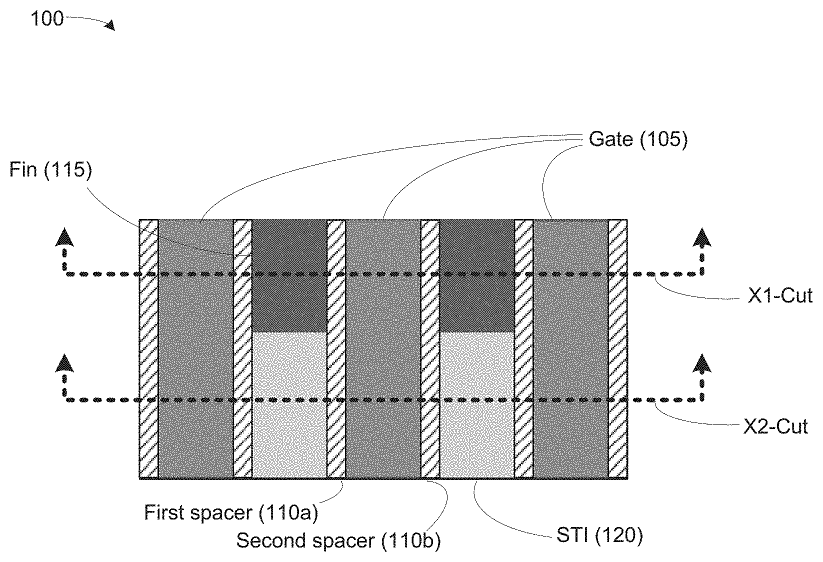
[0042] Turning now to FIG. 1, a stylized, simplified top or plan view of a semiconductor device 100 is illustrated. The semiconductor device 100 comprises at least one active area, e.g., fin 115 and at least one shallow trench isolation (STI) 120. The fin 115 and the STI 120 are generally rectangular in top view, and the long axis of the fin 115 and the long axis of the STI 120 are generally parallel.
[0043] For ease of illustration, only one fin 115 and one STI 120 are depicted in FIG. 1, however, the person of ordinary skill in the art will appreciate that the semiconductor device 100 may comprise a plurality of fins 115 and a plurality of STIs 120. Generally, in embodiments with more than one fin 115 and more than one STI 120, one STI 120 is disposed between two fins 115, and one fin 115 is disposed between two STIs 120.
[0044] The semiconductor device 100 also comprises at least one gate 105. The gate 105 is disposed over the fin 115 and the STI 120. The gate 105 is generally rectangular in top view, and the long axis of the gate 105 is generally perpendicular to the long axes of the fin 115 and the gate 120. As depicted, the semiconductor device 100 of FIG. 1 shows three gates 105; however, the person of ordinary skill in the art will understand that the semiconductor device 100 may comprise one, two, three, four, or more gates 105.
[0045] The semiconductor device 100 also comprises a first spacer 110a and a second spacer 110b. The spacers 110a and 110b may be referred to collectively as spacers 110. Each spacer 110 is disposed on one side of a gate 105.
[0046] The gate 105, the spacers 110, the fin 115, and the STI 120 may be formed of components and materials, and may be formed by processes, known to the person of ordinary skill in the art and which need not be described further.
[0047] FIG. 1 illustrates a semiconductor device 100 in a near-sighted view in which one or more structures overlying one or more of the gate 105, the spacers 110, the fin 115, and/or the STI 120 in an intermediate semiconductor device 100 or a finished semiconductor device 100 are omitted for clarity and brevity.
[0048] FIG. 1 also shows an X1-cut line and an X2-cut line provided for reference with respect to a cross-sectional view shown in subsequent figures. The X1-cut transects the gate 105, the spacers 110, and the fin 115 along the long axis of the fin 115. The X2-cut transects the gate 105, the spacers 110, and the STI 120 along the long axis of the STI 120. FIGS. 2-23 represent stylized cross-sectional views of finFET devices with respect to the X1-cut line or the X2-cut line, in accordance with exemplary embodiments herein.
[0049] Although embodiments depicted in FIGS. 1-23 show a FinFET device, the methods for constructing devices with short gate heights may be applied to the formation of other devices, such as fully-depeleted silicon on insulator (FDSOI) and planar FET devices. Such non-FinFET devices produced by methods disclosed herein are also encompassed by the present disclosure.
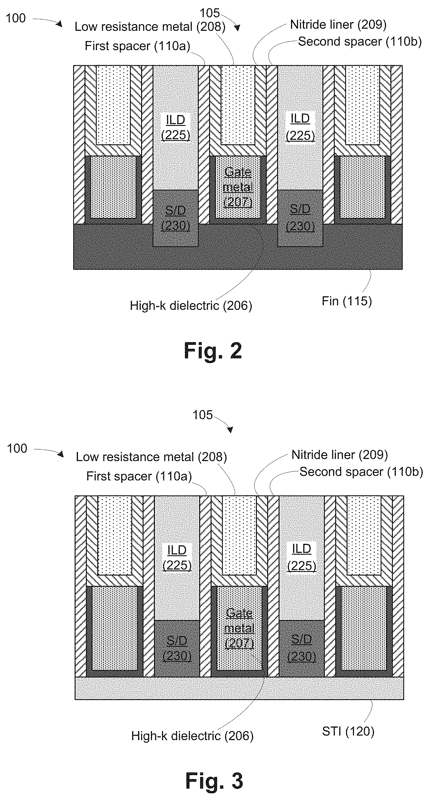
[0050] Turning to FIGS. 2-3, FIG. 2 illustrates a stylized depiction of an X1-cut cross-sectional view and FIG. 3 illustrates a stylized depiction of an X2-cut cross-sectional view of the semiconductor device 100 of FIG. 1 after a gate formation process, in accordance with embodiments herein. The gate formation process yields various components of the gate 105, including a high-k dielectric 206 on the bottom and lower portions of the sides of the gate 105; a gate metal 207; a nitride liner (e.g., titanium nitride) 209 on the gate metal 207 and upper portions of the sides of the gate 105; and a low resistance metal (e.g., tungsten) 208.
[0051] The semiconductor device 100 at this stage also comprises source/drains 230 disposed adjacent to the spacers 110. The sources/drains 230 have long axes running into and out of the view, generally parallel to the long axis of the gate 105. Surmounting the sources/drains 230 is an interlayer dielectric (ILD) 225. The ILD may be formed of silicon oxide, among other materials.
[0052] The gate 105 and sources/drains 230 are disposed over the fin 115 (as shown in FIG. 2) and the STI 120 (as shown in FIG. 3).
[0053] FIG. 4 illustrates a stylized depiction of an X1-cut cross-sectional view and FIG. 5 illustrates a stylized depiction of an X2-cut cross-sectional view of the semiconductor device 100 of FIGS. 2-3 after a gate recess process, in accordance with embodiments herein. In the gate recess process, the low resistance metal 208 and the nitride liner 209 are partially removed from the upper portion of the gate 105, to yield a recess 435. The bottom of the recess 435 is below the tops of the first spacer 110a and the second spacer 110b. The low resistance metal 208 and the nitride liner 209 may be partially removed by any appropriate technique to which the spacers 110 and the ILD 225 are resistant. The low resistance metal 208 and the nitride liner 209 may be partially removed in either order.
[0054] FIG. 6 illustrates a stylized depiction of an X1-cut cross-sectional view and FIG. 7 illustrates a stylized depiction of an X2-cut cross-sectional view of the semiconductor device 100 of FIGS. 4-5 after a silicon nitride deposition process, in accordance with embodiments herein. Silicon nitride 640 is conformally deposited, such as by atomic layer deposition (ALD), over the top of the semiconductor device 100. The silicon nitride 640 lines the bottom and sides of the recess 435 and the tops of the spacers 110 and the ILD 225.
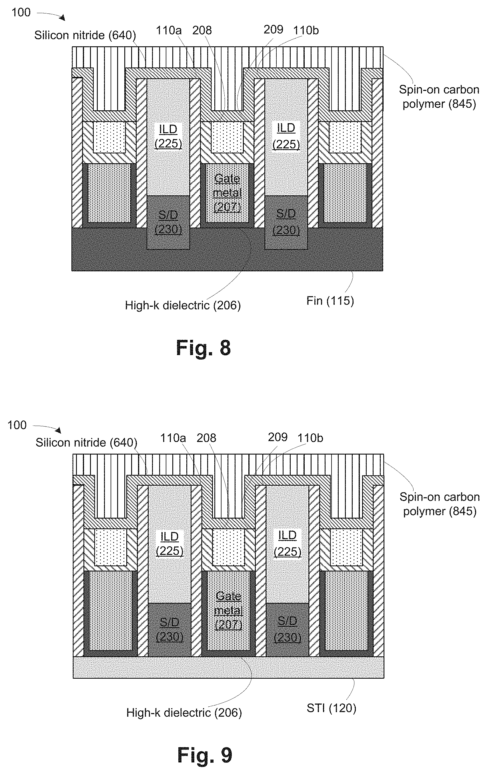
[0055] FIG. 8 illustrates a stylized depiction of an X1-cut cross-sectional view and FIG. 9 illustrates a stylized depiction of an X2-cut cross-sectional view of the semiconductor device 100 of FIGS. 6-7 after a spin-on carbon polymer deposition process, in accordance with embodiments herein. A spin-on carbon polymer 845 is deposited over the semiconductor device 100, overfilling the recess 435 and surmounting the spacers 110 and the ILD 225.
[0056] FIG. 10 illustrates a stylized depiction of an X1-cut cross-sectional view and FIG. 11 illustrates a stylized depiction of an X2-cut cross-sectional view of the semiconductor device 100 of FIGS. 8-9 after a spin-on carbon polymer recession process, in accordance with embodiments herein. The spin-on carbon polymer 845 is recessed to below the top of the first spacer 110a and the second spacer 110b, thereby yielding a recessed spin-on carbon polymer 1046 and a recess 1050. The sides of the recess 1050 are lined with the silicon nitride 640.
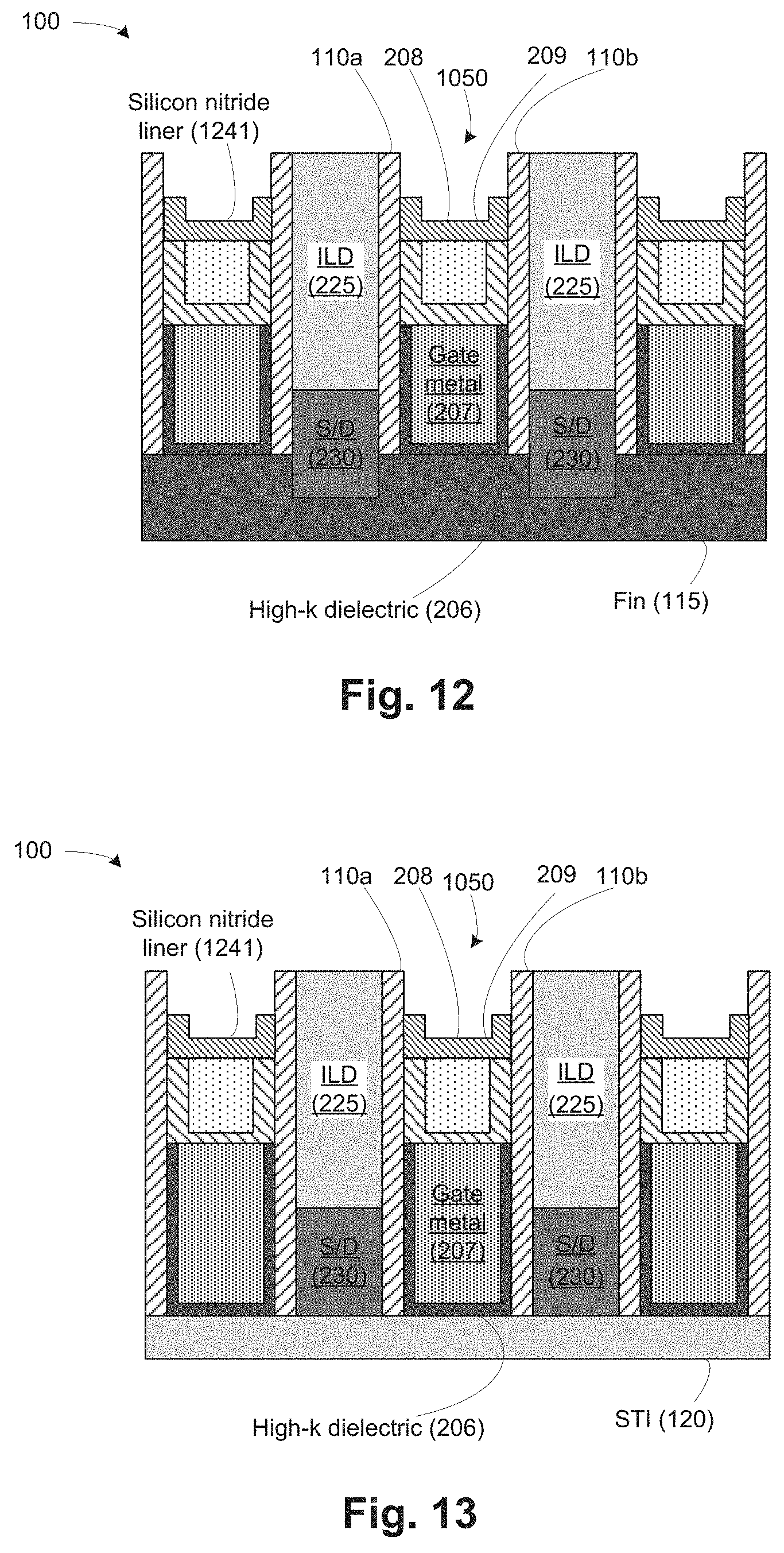
[0057] FIG. 12 illustrates a stylized depiction of an X1-cut cross-sectional view and FIG. 13 illustrates a stylized depiction of an X2-cut cross-sectional view of the semiconductor device 100 of FIGS. 10-11 after a silicon nitride recession and a spin-on carbon polymer removal process, in accordance with embodiments herein. In the silicon nitride recession process, the silicon nitride 640 is recessed to the top of the recessed spin-on carbon polymer 1046 of FIGS. 10-11. The recessed spin-on carbon polymer 1046 is then removed. As a result, the recess 1050 is deepened and widened relative to its depth and width in FIGS. 10-11. The spacers 110 now provide upper portions of the sidewalls of the recess 1050. The bottom and the lower portions of the sidewalls of the recess 1050 are provided by silicon nitride liner 1241.
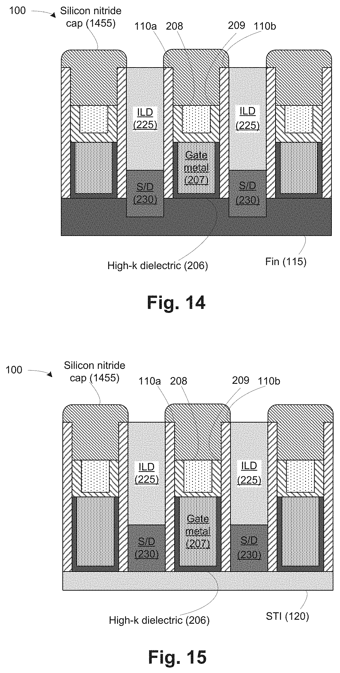
[0058] FIG. 14 illustrates a stylized depiction of an X1-cut cross-sectional view and FIG. 15 illustrates a stylized depiction of an X2-cut cross-sectional view of the semiconductor device 100 of FIGS. 12-13 after a cap formation process, in accordance with embodiments herein. In the cap formation process, a silicon nitride cap 1455 is grown selectively on the silicon nitride liner 1241. The silicon nitride liner 1241 is effectively subsumed into the silicon nitride cap 1455, and accordingly, the silicon nitride liner 1241 is not separately identified in FIGS. 14-23. The selective growth of the silicon nitride cap 1455 enables most, if not all, of the growth of the silicon nitride cap 1455 to fill the recess 1050 shown in FIGS. 12-13 and grow onto the top of the first spacer 110a and the second spacer 110b, with little or no growth of the silicon nitride cap 1455 over the ILD 225.
[0059] To effect selective growth of the silicon nitride cap 1455 on the silicon nitride liner 1241, the silicon nitride liner 1241 may be precleaned with diluted hydrofluoric acid (DHF) and the silicon nitride cap 1455 may be grown by silicon nitride deposition at a temperature of at least about 500.degree. C. In some embodiments, the silicon nitride cap 1455 may be grown by silicon nitride deposition at a temperature in the range of about 200.degree. C. to about 600.degree. C. The presence of the ILD 225 over the sources/drains 230 is expected to protect the sources/drains 230 from damage during the silicon nitride cap 1455 formation process.
[0060] FIG. 16 illustrates a stylized depiction of an X1-cut cross-sectional view and FIG. 17 illustrates a stylized depiction of an X2-cut cross-sectional view of the semiconductor device 100 of FIGS. 14-15 after an alternative cap formation process, in accordance with embodiments herein. In this alternative process, parameters are adjusted to encourage growth of a silicon nitride cap 1660 partially over the top of the ILD 225. In some embodiments, the growth time may be increased for forming a wider SiN cap. Though not to be bound by theory, the presence of the silicon nitride cap 1660 partially over the top of the ILD 225 may allow improved protection of the spacers 110 during later processing, relative to the silicon nitride cap 1455 shown in FIGS. 15-16.
[0061] FIG. 18 illustrates a stylized depiction of an X1-cut cross-sectional view and FIG. 19 illustrates a stylized depiction of an X2-cut cross-sectional view of the semiconductor device 100 of FIGS. 14-15 after a dielectric addition process, in accordance with embodiments herein. A dielectric material, which may but need not be the same material as the ILD 225, is formed on the semiconductor device 100. Doing so effectively increases the height of the ILD 225 to above the top of the silicon nitride cap 1455 (or the top of the silicon nitride cap 1660, if the dielectric addition process were performed on the semiconductor device 100 of FIGS. 16-17 (not shown.))
[0062] FIG. 20 illustrates a stylized depiction of an X1-cut cross-sectional view and FIG. 21 illustrates a stylized depiction of an X2-cut cross-sectional view of the semiconductor device 100 of FIGS. 18-19 after a dielectric planarization process, in accordance with embodiments herein. Planarization of the ILD 225 to be coplanar with the top of the silicon nitride cap 1455 may involve chemical mechanical polishing (CMP).
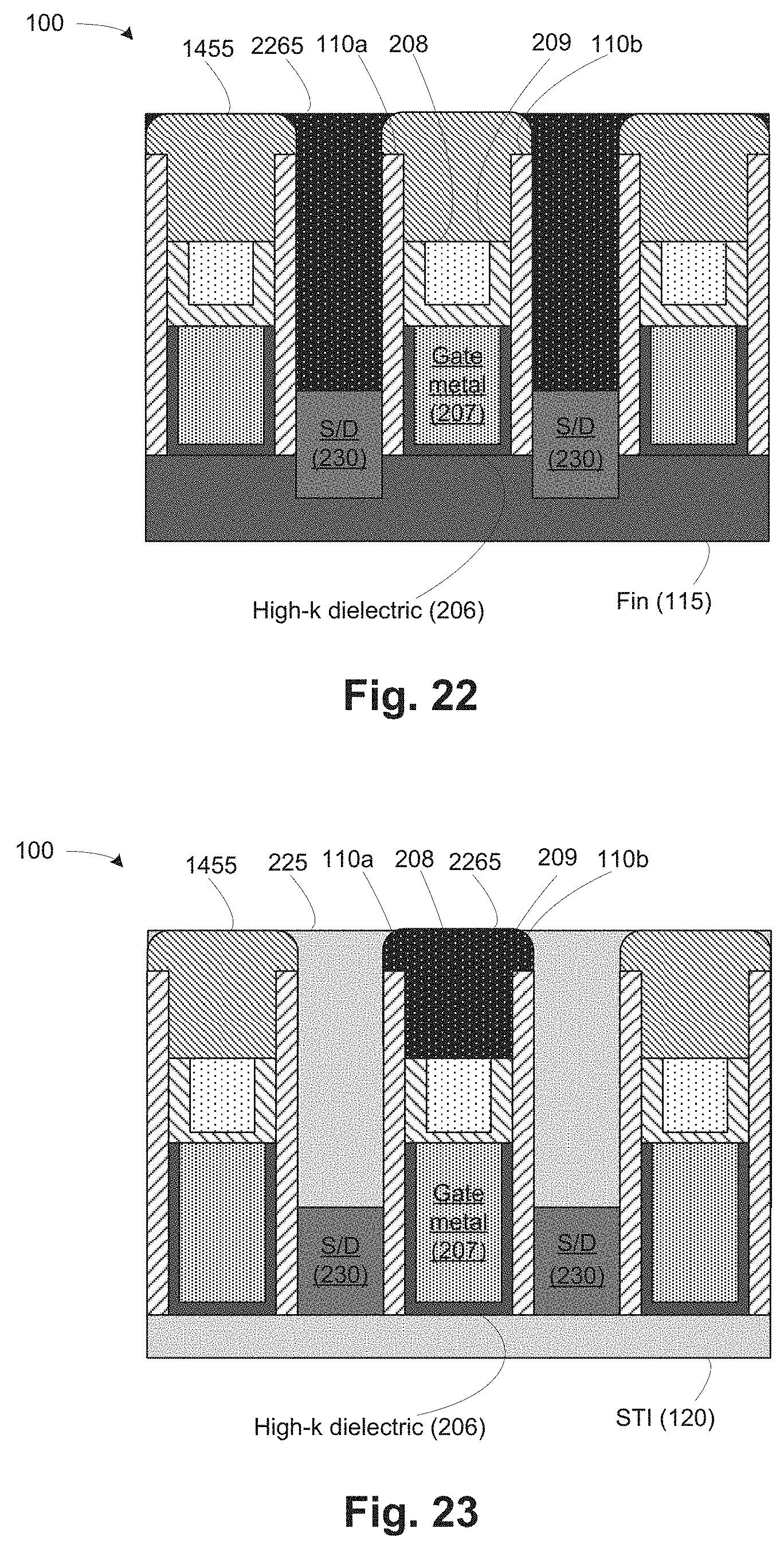
[0063] FIG. 22 illustrates a stylized depiction of an X1-cut cross-sectional view and FIG. 23 illustrates a stylized depiction of an X2-cut cross-sectional view of the semiconductor device 100 of FIGS. 20-21 after a contact formation process, in accordance with embodiments herein. In this process, at least a portion of ILD 225 is removed over the fin 155 to expose at least a portion of each source/drain 230 (FIG. 22) and at least a portion of the gate 105 is removed over the STI 120 to expose at least a portion of the low resistance metal 208 and the nitride liner 209 (FIG. 23). Subsequently, contacts 2265 are formed to contact the source/drains 230 (FIG. 22) and the low resistance metal 208 (FIG. 23) in the spaces where the ILD 225 and the gate 105 were removed. The contact formation process depicted in FIGS. 22-23 may be considered a self-aligned contact formation process.
[0064] After the contact formation depicted in FIGS. 21-22, further processing events may be performed to prepare the semiconductor device 100 for an intended use. For example, metallization layers and other structures may be formed above the semiconductor device 100 shown in FIGS. 21-22. Such additional steps may be routinely implemented by the person of ordinary skill in the art having the benefit of the present disclosure.
[0065] FIG. 24 illustrates a flowchart depiction of a method 2400 for manufacturing a device, in accordance with embodiments herein. The method 2400 comprises forming (at 2410) a gate over at least one fin disposed on a semiconductor substrate. The method 2400 additionally comprises forming (at 2415) a first spacer disposed on one gate sidewall and a second spacer disposed on another gate sidewall. The method 2400 further comprises forming (at 2420) a dielectric material adjacent the first spacer and adjacent the second spacer.
[0066] The method 2400 also comprises recessing (at 2425) the gate to below a top of the first spacer and a top of the second spacer. The method 2400 additionally comprises forming (at 2430) a silicon nitride liner on a top of the recessed gate.
[0067] In one embodiment, the forming (at 2430) the silicon nitride liner may comprise depositing by atomic layer deposition (ALD) of silicon nitride on a top of the recessed gate, on an exposed sidewall portion and a top of the first spacer, on an exposed sidewall portion and a top of the second spacer, and on a top of the dielectric material; coating the silicon nitride with a spin-on carbon polymer; recessing the spin-on carbon polymer to below the top of the first spacer and the top of the second spacer, to yield recessed spin-on carbon polymer; removing the silicon nitride above the recessed spin-on carbon polymer, to yield the silicon nitride liner; and removing the recessed spin-on carbon polymer.
[0068] The method 2400 yet also comprises growing (at 2435) a silicon nitride cap selectively on the silicon nitride liner and at least on a top of the first spacer and a top of the second spacer.
[0069] In one embodiment, the growing (at 2435) the silicon nitride cap may comprise treating the dielectric material to prevent silicon nitride growth on the dielectric material. Alternatively or in addition, the growing (at 2435) the silicon nitride cap may further comprise growth of silicon nitride over a portion of the dielectric material.
[0070] The method 2400 additionally further comprises extending (at 2440) the dielectric material to the same height as the silicon nitride cap.
[0071] In one embodiment, the extending (at 2440) the dielectric material to the same height as the silicon nitride cap may comprise overfilling a gap adjacent to the silicon nitride cap with the dielectric material and performing chemical mechanical polishing (CMP) to planarize the dielectric material to a top of the silicon nitride cap.
[0072] Finally, the method 2400 yet additionally comprises forming (at 2445) contacts to the gate and the fin, wherein contact formation is self-aligned by the silicon nitride cap.
[0073] In one embodiment, the forming (at 2445) the contacts to the gate and to the fin comprises forming the contact to the gate at a position disposed laterally away from the fin. For example, the contact to the gate may be formed over an STI disposed laterally away from the fin.
[0074] In one embodiment, in the forming (at 2420) and the extending (at 2440) the dielectric material, the dielectric material may be silicon oxide.
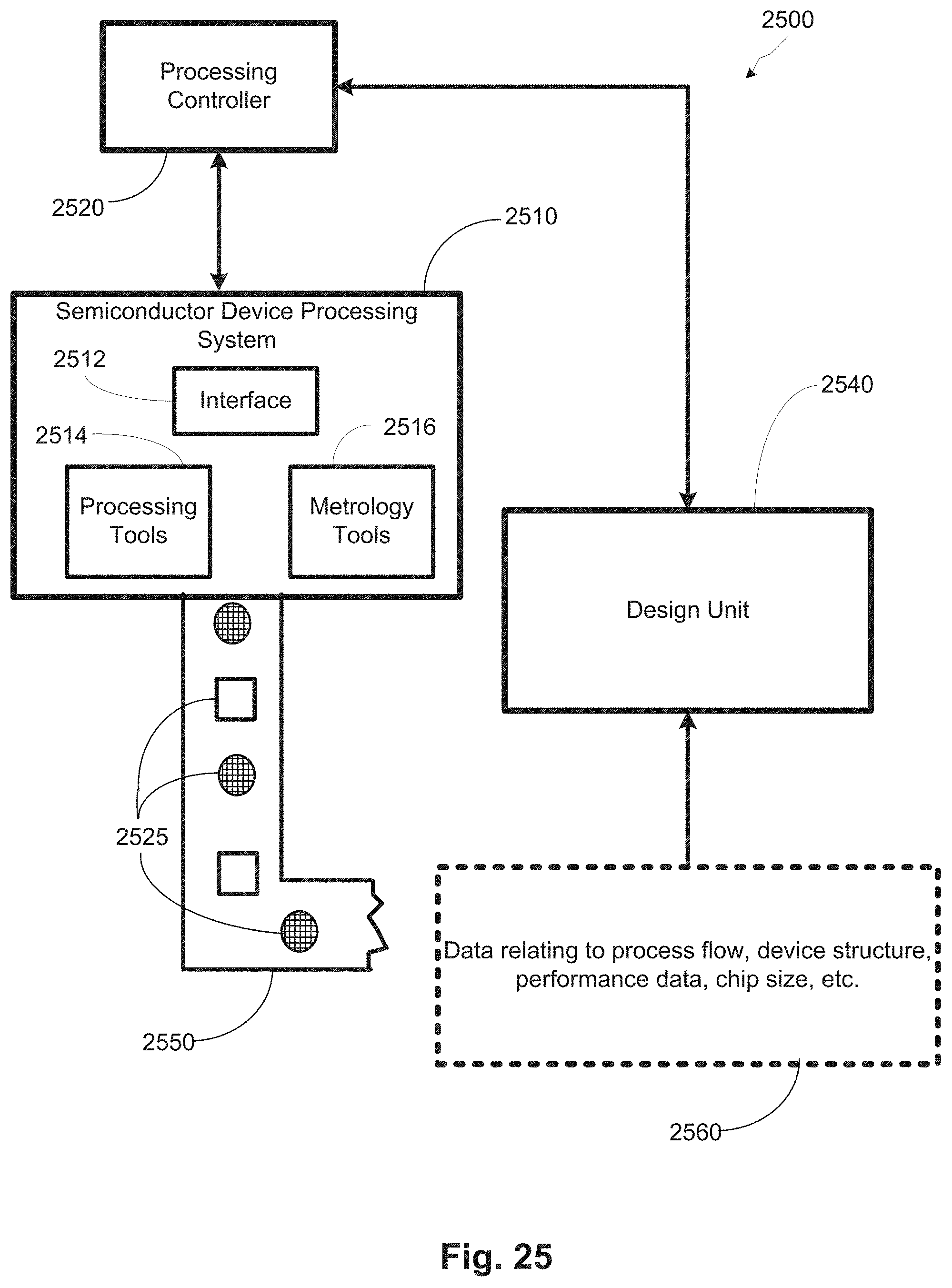
[0075] Turning now to FIG. 25, a stylized depiction of a system for fabricating a semiconductor device, in accordance with embodiments herein, is illustrated. The system 2500 provides for semiconductor devices comprising a silicon nitride cap enabling a self-aligned contact formation process.
[0076] The system 2500 of FIG. 25 may comprise a semiconductor device processing system 2510 and a design unit 2540. The semiconductor device processing system 2510 may manufacture integrated circuit devices based upon one or more designs provided by the design unit 2540.
[0077] The semiconductor device processing system 2510 may comprise various processing tools 2514, such as etch process stations, photolithography process stations, oxide deposition process stations, CMP process stations, Epitaxy (EPI) process stations, etc. The semiconductor device processing system 2510 may also comprise one or more metrology tools 2516. One or more of the processing steps performed by the processing system 2510 may be controlled by the processing controller 2520. The processing controller 2520 may be a workstation computer, a desktop computer, a laptop computer, a tablet computer, or any other type of computing device comprising one or more software products that are capable of controlling processes, receiving process feedback, receiving test results data, performing learning cycle adjustments, performing process adjustments, etc. Generally, the processing controller 2520 may communicate to the semiconductor device processing system 2510 via an interface 2512.
[0078] The semiconductor device processing system 2510 may produce semiconductor devices on a medium, such as silicon wafers. More particularly, the semiconductor device processing system 2510 may produce semiconductor devices as described above.
[0079] The production of integrated circuits by the device processing system 2510 may be based upon the circuit designs provided by the integrated circuits design unit 2540. The processing system 2510 may provide processed integrated circuits/devices 2525 on a transport mechanism 2550, such as a conveyor system. In some embodiments, the conveyor system may be sophisticated clean room transport systems that are capable of transporting semiconductor wafers.
[0080] In some embodiments, the items labeled "2525" may represent individual wafers, and in other embodiments, the items 2525 may represent a group of semiconductor wafers, e.g., a "lot" of semiconductor wafers. The semiconductor device 2525 may be a transistor, a capacitor, a resistor, a memory cell, a processor, and/or the like.
[0081] The design unit 2540 of the system 2500 is capable of providing a circuit design that may be manufactured by the semiconductor processing system 2510. The design unit 2540 may be capable of determining the number of devices (e.g., processors, memory devices, etc.) to place in a device package, silicon nitride liner formation specifications, silicon nitride liner treatment specifications, silicon nitride cap formation specifications, and other process specifications. Based at least upon these specifications, the design unit 2540 may provide data for manufacturing a semiconductor device in accordance with embodiments herein.
[0082] The system 2500 may be capable of performing analysis and manufacturing of various products involving various technologies. For example, the system 2500 may design and manufacturing-data for manufacturing devices of CMOS technology, Flash technology, BiCMOS technology, power devices, memory devices (e.g., DRAM devices), NAND memory devices, and/or various other semiconductor technologies.
[0083] The particular embodiments disclosed above are illustrative only, as the invention may be modified and practiced in different but equivalent manners apparent to those skilled in the art having the benefit of the teachings herein. For example, the process steps set forth above may be performed in a different order. Furthermore, no limitations are intended to the details of construction or design herein shown, other than as described in the claims below. It is therefore evident that the particular embodiments disclosed above may be altered or modified and all such variations are considered within the scope and spirit of the invention. Accordingly, the protection sought herein is as set forth in the claims below.
* * * * *
D00000
D00001
D00002
D00003
D00004
D00005
D00006
D00007
D00008
D00009
D00010
D00011
D00012
D00013

D00014
XML
uspto.report is an independent third-party trademark research tool that is not affiliated, endorsed, or sponsored by the United States Patent and Trademark Office (USPTO) or any other governmental organization. The information provided by uspto.report is based on publicly available data at the time of writing and is intended for informational purposes only.
While we strive to provide accurate and up-to-date information, we do not guarantee the accuracy, completeness, reliability, or suitability of the information displayed on this site. The use of this site is at your own risk. Any reliance you place on such information is therefore strictly at your own risk.
All official trademark data, including owner information, should be verified by visiting the official USPTO website at www.uspto.gov. This site is not intended to replace professional legal advice and should not be used as a substitute for consulting with a legal professional who is knowledgeable about trademark law.