Selective Nitride Removal
Goradia; Prerna Sonthalia ; et al.
U.S. patent application number 16/399391 was filed with the patent office on 2019-10-31 for selective nitride removal. This patent application is currently assigned to Applied Materials, Inc.. The applicant listed for this patent is Applied Materials, Inc.. Invention is credited to Geetika Bajaj, Prerna Sonthalia Goradia, Nitin K. Ingle, Yogita Pareek, Robert Jan Visser.
| Application Number | 20190333776 16/399391 |
| Document ID | / |
| Family ID | 68292815 |
| Filed Date | 2019-10-31 |


| United States Patent Application | 20190333776 |
| Kind Code | A1 |
| Goradia; Prerna Sonthalia ; et al. | October 31, 2019 |
SELECTIVE NITRIDE REMOVAL
Abstract
Exemplary methods for selective etching of semiconductor materials may include flowing a fluorine-containing precursor into a processing region of a semiconductor processing chamber. The methods may also include flowing a silicon-containing suppressant into the processing region of the semiconductor processing chamber. The methods may further include contacting a substrate with the fluorine-containing precursor and the silicon-containing suppressant. The substrate may include an exposed region of silicon nitride and an exposed region of silicon oxide. The methods may also include selectively etching the exposed region of silicon nitride to the exposed region of silicon oxide.
| Inventors: | Goradia; Prerna Sonthalia; (Mumbai, IN) ; Pareek; Yogita; (San Jose, CA) ; Bajaj; Geetika; (New Delhi, IN) ; Visser; Robert Jan; (Menlo Park, CA) ; Ingle; Nitin K.; (San Jose, CA) | ||||||||||
| Applicant: |
|
||||||||||
|---|---|---|---|---|---|---|---|---|---|---|---|
| Assignee: | Applied Materials, Inc. Santa Clara CA |
||||||||||
| Family ID: | 68292815 | ||||||||||
| Appl. No.: | 16/399391 | ||||||||||
| Filed: | April 30, 2019 |
Related U.S. Patent Documents
| Application Number | Filing Date | Patent Number | ||
|---|---|---|---|---|
| 62664724 | Apr 30, 2018 | |||
| Current U.S. Class: | 1/1 |
| Current CPC Class: | H01J 37/32091 20130101; H01L 21/31116 20130101; H01L 21/67167 20130101; H01L 21/67069 20130101; H01J 37/32422 20130101; H01J 37/3244 20130101; H01J 37/32467 20130101; H01J 37/32357 20130101 |
| International Class: | H01L 21/311 20060101 H01L021/311; H01L 21/67 20060101 H01L021/67 |
Claims
1. An etching method comprising: flowing a fluorine-containing precursor into a processing region of a semiconductor processing chamber; flowing a silicon-containing suppressant into the processing region of the semiconductor processing chamber; contacting a substrate with the fluorine-containing precursor and the silicon-containing suppressant, wherein the substrate comprises an exposed region of silicon nitride and an exposed region of silicon oxide; and selectively etching the exposed region of silicon nitride to the exposed region of silicon oxide.
2. The etching method of claim 1, wherein the processing region of the semiconductor processing chamber is maintained water-free while contacting the substrate with the fluorine-containing precursor and the silicon-containing suppressant.
3. The etching method of claim 1, wherein the fluorine-containing precursor comprises anhydrous hydrogen fluoride.
4. The etching method of claim 1, wherein the silicon-containing suppressant comprises silicon fluoride.
5. The etching method of claim 4, wherein the silicon-containing suppressant comprises at least one of silicon tetrafluoride, disilicon hexafluoride, or trisilicon octafluoride.
6. The etching method of claim 1, wherein the silicon-containing suppressant comprises hexafluorosilicic acid.
7. The etching method of claim 1, wherein the etching method removes the exposed region of silicon nitride at a rate of at least about 10 .ANG. per minute.
8. The etching method of claim 1, wherein the etching method has a selectivity of silicon nitride to silicon oxide greater than or about 50:1.
9. The etching method of claim 1, wherein the exposed region of silicon oxide comprises low-density silicon oxide.
10. The etching method of claim 1, wherein the substrate further comprises an exposed region of silicon, the etching method further comprising: selectively etching the exposed region of silicon nitride to the exposed region of silicon, wherein the etching method has a selectivity of silicon nitride to silicon greater than or about 50:1.
11. The etching method of claim 1, wherein the fluorine-containing precursor and the silicon-containing suppressant are flowed into the processing region for a time period of less than or about 10 minutes.
12. The etching method of claim 1, wherein a temperature of the substrate is maintained between about 25.degree. C. and about 250.degree. C. during the etching method.
13. The etching method of claim 12, wherein a temperature of the substrate is maintained between about 100.degree. C. and about 150.degree. C. during the etching method.
14. The etching method of claim 1, wherein a ratio of a flow rate of the fluorine-containing precursor to a flow rate of the silicon-containing suppressant is about 10:1.
15. An etching method comprising: flowing anhydrous hydrogen fluoride into a processing region of a semiconductor processing chamber; flowing a silicon-containing suppressant into the processing region of the semiconductor processing chamber; contacting a substrate with the anhydrous hydrogen fluoride and the silicon-containing suppressant, wherein the substrate comprises an exposed region of silicon nitride and an exposed region of silicon oxide; and selectively etching the exposed region of silicon nitride at a rate of at least about 10 .ANG. per minute, wherein the etching method has a selectivity of silicon nitride to silicon oxide greater than or about 50:1; wherein a temperature of the substrate is maintained between about 100.degree. C. and about 150.degree. C. during the etching of the exposed region of silicon nitride.
16. The etching method of claim 15, wherein the silicon-containing suppressant comprises at least one of silicon fluoride or hexafluorosilicic acid.
17. The etching method of claim 15, wherein the processing region is maintained water-free while contacting the substrate with the anhydrous hydrogen fluoride and the silicon-containing suppressant.
18. An etching method comprising: flowing anhydrous hydrogen fluoride into a processing region of a semiconductor processing chamber; flowing silicon fluoride into the processing region of the semiconductor processing chamber; contacting a substrate with the anhydrous hydrogen fluoride and the silicon fluoride, wherein the substrate comprises an exposed region of silicon nitride and an exposed region of silicon oxide; and selectively etching the exposed region of silicon nitride to the exposed region of silicon oxide, wherein the etching method has a selectivity of silicon nitride to silicon oxide greater than or about 50:1; wherein a temperature of the substrate is maintained between about 100.degree. C. and about 150.degree. C. during the etching of the exposed region of silicon nitride; and wherein the processing region is maintained water-free while contacting the substrate with the anhydrous hydrogen fluoride and the silicon fluoride.
19. The etching method of claim 18, wherein the silicon fluoride comprises at least one of silicon tetrafluoride, disilicon hexafluoride, or trisilicon octafluoride.
20. The etching method of claim 18, wherein a ratio of a flow rate of the anhydrous hydrogen fluoride to a flow rate of the silicon fluoride is about 10:1.
Description
CROSS-REFERENCES TO RELATED APPLICATIONS
[0001] This application claims the benefit of U.S. Provisional Patent Application No. 62/664,724, filed on Apr. 30, 2018, and which is hereby incorporated by reference in its entirety for all purposes.
TECHNICAL FIELD
[0002] The present technology relates to semiconductor processes and equipment. More specifically, the present technology relates to selective etching of nitride materials.
BACKGROUND
[0003] Integrated circuits are made possible by processes which produce intricately patterned material layers on substrate surfaces. Producing patterned material on a substrate requires controlled methods for removal of exposed material. Chemical etching is used for a variety of purposes including transferring a pattern in photoresist into underlying layers, thinning layers, or thinning lateral dimensions of features already present on the surface. Often it is desirable to have an etch process that etches one material faster than another facilitating, for example, a pattern transfer process. Such an etch process is said to be selective to the first material. As a result of the diversity of materials, circuits, and processes, etch processes have been developed with a selectivity towards a variety of materials.
[0004] Etch processes may be termed wet or dry based on the materials used in the process. A wet HF etch preferentially removes silicon oxide over other dielectrics and materials. However, wet processes may have difficulty penetrating some constrained trenches and also may sometimes deform the remaining material. Dry etches produced in local plasmas formed within the substrate processing region can penetrate more constrained trenches and exhibit less deformation of delicate remaining structures. However, local plasmas may damage the substrate through the production of electric arcs as they discharge.
[0005] Thus, there is a need for improved systems and methods that can be used to produce high quality devices and structures. These and other needs are addressed by the present technology.
SUMMARY
[0006] Exemplary etching methods may include flowing a fluorine-containing precursor into a processing region of a semiconductor processing chamber. The methods may also include flowing a silicon-containing suppressant into the processing region of the semiconductor processing chamber. The methods may further include contacting a substrate with the fluorine-containing precursor and the silicon-containing suppressant. The substrate may include an exposed region of silicon nitride and an exposed region of silicon oxide. The methods may further include selectively etching the exposed region of silicon nitride to the exposed region of silicon oxide.
[0007] In some embodiments, the processing region of the semiconductor processing chamber may be maintained water-free while contacting the substrate with the fluorine-containing precursor and the silicon-containing suppressant. In some embodiments, the fluorine-containing precursor may include anhydrous hydrogen fluoride. In some embodiments, the silicon-containing suppressant may include silicon fluoride. In some embodiments, the silicon-containing suppressant may include at least one of silicon tetrafluoride, disilicon hexafluoride, or trisilicon octafluoride. In some embodiments, the silicon-containing suppressant may include hexafluorosilicic acid. In some embodiments, the etching method may remove the exposed region of silicon nitride at a rate of at least about 10 .ANG. per minute. In some embodiments, the etching method may have a selectivity of silicon nitride to silicon oxide greater than or about 50:1. In some embodiments, the exposed region of silicon oxide may include low-density silicon oxide.
[0008] In some embodiments, the substrate may further include an exposed region of silicon. The etching method further may include selectively etching the exposed region of silicon nitride to the exposed region of silicon. The etching method may have a selectivity of silicon nitride to silicon greater than or about 50:1.
[0009] In some embodiments, the fluorine-containing precursor and the silicon-containing suppressant may be flowed into the processing region for a time period of less than or about 10 minutes. In some embodiments, a temperature of the substrate may be maintained between about 25.degree. C. and about 250.degree. C. during the etching methods. In some embodiments, a temperature of the substrate may be maintained between about 100.degree. C. and about 150.degree. C. during the etching methods. In some embodiments, a ratio of a flow rate of the fluorine-containing precursor to a flow rate of the silicon-containing suppressant may be about 10:1.
[0010] The present technology may include additional etching methods. The methods may include flowing anhydrous hydrogen fluoride into a processing region of a semiconductor processing chamber. The methods may further include flowing a silicon-containing suppressant into the processing region of the semiconductor processing chamber. The methods may also include contacting a substrate with the anhydrous hydrogen fluoride and the silicon-containing suppressant. The substrate may include an exposed region of silicon nitride and an exposed region of silicon oxide. The methods may further include selectively etching the exposed region of silicon nitride at a rate of at least about 10 .ANG. per minute. The etching method may have a selectivity of silicon nitride to silicon oxide greater than or about 50:1. A temperature of the substrate may be maintained between about 100.degree. C. and about 150.degree. C. during the etching of the exposed region of silicon nitride. The silicon-containing suppressant may include at least one of silicon fluoride or hexafluorosilicic acid. The processing region may be maintained water-free while contacting the substrate with the anhydrous hydrogen fluoride and the silicon-containing suppressant.
[0011] The present technology may include further etching methods. The methods may include flowing anhydrous hydrogen fluoride into a processing region of a semiconductor processing chamber. The methods may further include flowing silicon fluoride into the processing region of the semiconductor processing chamber. The methods may also include contacting a substrate with the anhydrous hydrogen fluoride and the silicon fluoride. The substrate may include an exposed region of silicon nitride and an exposed region of silicon oxide. The methods may further include selectively etching the exposed region of silicon nitride to the exposed region of silicon oxide. The etching method may have a selectivity of silicon nitride to silicon oxide greater than or about 50:1. A temperature of the substrate may be maintained between about 100.degree. C. and about 150.degree. C. during the etching of the exposed region of silicon nitride. The processing region may be maintained water-free while contacting the substrate with the anhydrous hydrogen fluoride and the silicon fluoride.
[0012] In some embodiments, the silicon fluoride may include at least one of silicon tetrafluoride, disilicon hexafluoride, or trisilicon octafluoride. In some embodiments, a ratio of a flow rate of the anhydrous hydrogen fluoride to a flow rate of the silicon fluoride may be about 10:1.
[0013] Such technology may provide numerous benefits over conventional systems and techniques. For example, the present technology provides a gas-phase chemistry that may etch silicon nitride sufficiently fast and selective to silicon oxide, silicon, and other exposed films on a substrate. Additionally, the present technology provides chemistry-based etching methods that may not involve high-energy plasma, and thus prevent feature damages that may be caused by ion bombardment. These and other embodiments, along with many of their advantages and features, are described in more detail in conjunction with the below description and attached figures.
BRIEF DESCRIPTION OF THE DRAWINGS
[0014] A further understanding of the nature and advantages of the disclosed technology may be realized by reference to the remaining portions of the specification and the drawings.
[0015] FIG. 1 shows a top plan view of one embodiment of an exemplary processing tool according to some embodiments of the present technology.
[0016] FIG. 2A shows a schematic cross-sectional view of an exemplary processing chamber according to embodiments of the present technology.
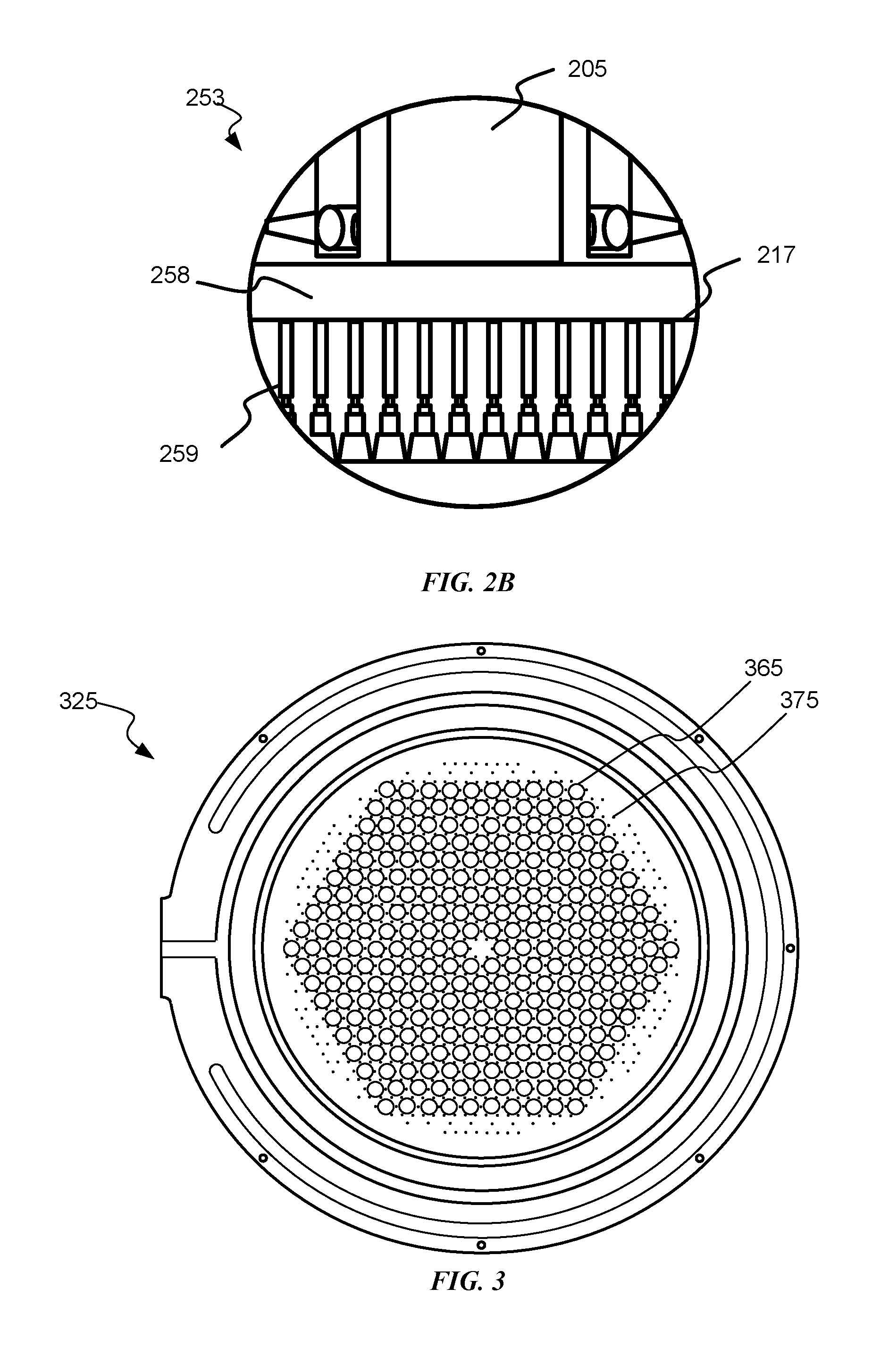
[0017] FIG. 2B shows a detailed view of a portion of the processing chamber illustrated in FIG. 2A according to embodiments of the present technology.
[0018] FIG. 3 shows a bottom plan view of an exemplary showerhead according to embodiments of the present technology.
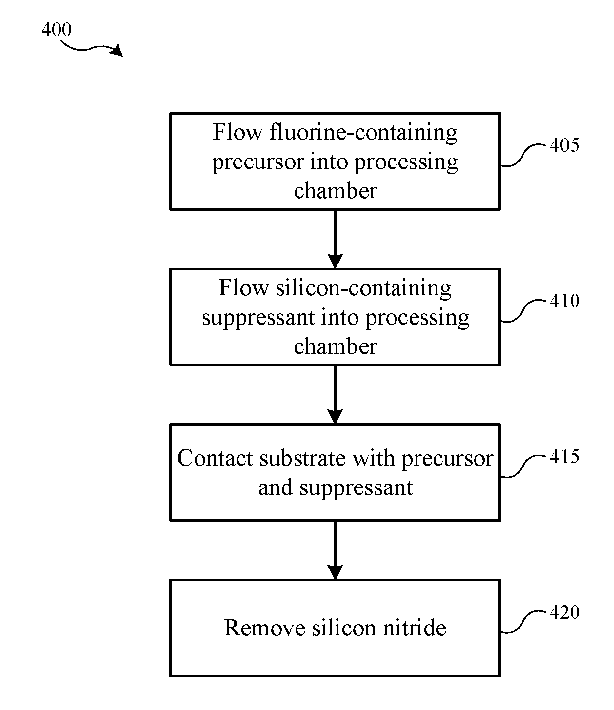
[0019] FIG. 4 shows exemplary operations in a method according to some embodiments of the present technology.
[0020] Several of the figures are included as schematics. It is to be understood that the figures are for illustrative purposes, and are not to be considered of scale unless specifically stated to be of scale. Additionally, as schematics, the figures are provided to aid comprehension and may not include all aspects or information compared to realistic representations, and may include exaggerated material for illustrative purposes.
[0021] In the appended figures, similar components and/or features may have the same reference label. Further, various components of the same type may be distinguished by following the reference label by a letter that distinguishes among the similar components. If only the first reference label is used in the specification, the description is applicable to any one of the similar components having the same first reference label irrespective of the letter.
DETAILED DESCRIPTION
[0022] As semiconductor device features continue to reduce in size, processes that offer high etch selectivity and precise control of the amount of material to be removed become more desirable. In some applications, such as VNAND devices, silicon nitride may be removed selectively in the presence of silicon oxide, silicon, and/or other materials. Wet etching may offer desired control and selectivity. However, a large quantity of chemicals may be consumed in wet etching methods and a cleaning operation may be required after the etching operation. High-energy plasma based etching methods, such as reactive-ion etching (ME), have been explored for improved selectivity and control. However, these high-energy plasma based etching methods lack the ability of isotropic etching, and ion bombardment involved in these methods may cause damage to device structures.
[0023] The present technology overcomes these and other issues by providing a gas-phase chemistry that may etch silicon nitride sufficiently fast and selective to silicon oxide, silicon, and other exposed films on a substrate. The present technology provides chemistry-based etching methods that do not involve high-energy plasma, and thus prevent feature damages that may be caused by ion bombardment.
[0024] Although the remaining disclosure will routinely identify specific etching processes utilizing the disclosed technology, it will be readily understood that the systems and methods are equally applicable to deposition and cleaning processes as may occur in the described chambers. Accordingly, the technology should not be considered to be so limited as for use with etching processes or chambers alone. Moreover, although an exemplary chamber is described to provide foundation for the present technology, it is to be understood that the present technology can be applied to virtually any semiconductor processing chamber that may allow the single-chamber operations described.
[0025] FIG. 1 shows a top plan view of one embodiment of a processing system 100 of deposition, etching, baking, and curing chambers according to embodiments. In the figure, a pair of front opening unified pods (FOUPs) 102 supply substrates of a variety of sizes that are received by robotic arms 104 and placed into a low pressure holding area 106 before being placed into one of the substrate processing chambers 108a-f, positioned in tandem sections 109a-c. A second robotic arm 110 may be used to transport the substrate wafers from the holding area 106 to the substrate processing chambers 108a-f and back. Each substrate processing chamber 108a-f, can be outfitted to perform a number of substrate processing operations including the dry etch processes described herein in addition to cyclical layer deposition (CLD), atomic layer deposition (ALD), chemical vapor deposition (CVD), physical vapor deposition (PVD), etch, pre-clean, degas, orientation, and other substrate processes.
[0026] The substrate processing chambers 108a-f may include one or more system components for depositing, annealing, curing and/or etching a dielectric or metallic film on the substrate wafer. In one configuration, two pairs of the processing chambers, e.g., 108c-d and 108e-f, may be used to deposit material on the substrate, and the third pair of processing chambers, e.g., 108a-b, may be used to etch the deposited material. In another configuration, all three pairs of chambers, e.g., 108a-f, may be configured to etch a dielectric or metallic film on the substrate. Any one or more of the processes described may be carried out in chamber(s) separated from the fabrication system shown in different embodiments. It will be appreciated that additional configurations of deposition, etching, annealing, and curing chambers for dielectric films are contemplated by system 100.
[0027] FIG. 2A shows a cross-sectional view of an exemplary process chamber system 200 with partitioned plasma generation regions within the processing chamber. During film etching, e.g., titanium nitride, tantalum nitride, tungsten, copper, cobalt, silicon, polysilicon, silicon oxide, silicon nitride, silicon oxynitride, silicon oxycarbide, etc., a process gas may be flowed into the first plasma region 215 through a gas inlet assembly 205. A remote plasma system (RPS) 201 may optionally be included in the system, and may process a first gas which then travels through gas inlet assembly 205. The inlet assembly 205 may include two or more distinct gas supply channels where the second channel (not shown) may bypass the RPS 201, if included.
[0028] A cooling plate 203, faceplate 217, ion suppressor 223, showerhead 225, and a substrate support 265, having a substrate 255 disposed thereon, are shown and may each be included according to embodiments. The pedestal 265 may have a heat exchange channel through which a heat exchange fluid flows to control the temperature of the substrate, which may be operated to heat and/or cool the substrate or wafer during processing operations. The wafer support platter of the pedestal 265, which may comprise aluminum, ceramic, or a combination thereof, may also be resistively heated in order to achieve relatively high temperatures, such as from up to or about 100.degree. C. to above or about 600.degree. C., using an embedded resistive heater element.
[0029] The faceplate 217 may be pyramidal, conical, or of another similar structure with a narrow top portion expanding to a wide bottom portion. The faceplate 217 may additionally be flat as shown and include a plurality of through-channels used to distribute process gases. Plasma generating gases and/or plasma excited species, depending on use of the RPS 201, may pass through a plurality of holes, shown in FIG. 2B, in faceplate 217 for a more uniform delivery into the first plasma region 215.
[0030] Exemplary configurations may include having the gas inlet assembly 205 open into a gas supply region 258 partitioned from the first plasma region 215 by faceplate 217 so that the gases/species flow through the holes in the faceplate 217 into the first plasma region 215. Structural and operational features may be selected to prevent significant backflow of plasma from the first plasma region 215 back into the supply region 258, gas inlet assembly 205, and fluid supply system 210. The faceplate 217, or a conductive top portion of the chamber, and showerhead 225 are shown with an insulating ring 220 located between the features, which allows an AC potential to be applied to the faceplate 217 relative to showerhead 225 and/or ion suppressor 223. The insulating ring 220 may be positioned between the faceplate 217 and the showerhead 225 and/or ion suppressor 223 enabling a capacitively coupled plasma (CCP) to be formed in the first plasma region. A baffle (not shown) may additionally be located in the first plasma region 215, or otherwise coupled with gas inlet assembly 205, to affect the flow of fluid into the region through gas inlet assembly 205.
[0031] The ion suppressor 223 may comprise a plate or other geometry that defines a plurality of apertures throughout the structure that are configured to suppress the migration of ionically-charged species out of the first plasma region 215 while allowing uncharged neutral or radical species to pass through the ion suppressor 223 into an activated gas delivery region between the suppressor and the showerhead. In embodiments, the ion suppressor 223 may comprise a perforated plate with a variety of aperture configurations. These uncharged species may include highly reactive species that are transported with less reactive carrier gas through the apertures. As noted above, the migration of ionic species through the holes may be reduced, and in some instances completely suppressed. Controlling the amount of ionic species passing through the ion suppressor 223 may advantageously provide increased control over the gas mixture brought into contact with the underlying wafer substrate, which in turn may increase control of the deposition and/or etch characteristics of the gas mixture. For example, adjustments in the ion concentration of the gas mixture can significantly alter its etch selectivity, e.g., SiNx:SiOx etch ratios, Si:SiOx etch ratios, etc. In alternative embodiments in which deposition is performed, it can also shift the balance of conformal-to-flowable style depositions for dielectric materials.
[0032] The plurality of apertures in the ion suppressor 223 may be configured to control the passage of the activated gas, i.e., the ionic, radical, and/or neutral species, through the ion suppressor 223. For example, the aspect ratio of the holes, or the hole diameter to length, and/or the geometry of the holes may be controlled so that the flow of ionically-charged species in the activated gas passing through the ion suppressor 223 is reduced. The holes in the ion suppressor 223 may include a tapered portion that faces the plasma excitation region 215, and a cylindrical portion that faces the showerhead 225. The cylindrical portion may be shaped and dimensioned to control the flow of ionic species passing to the showerhead 225. An adjustable electrical bias may also be applied to the ion suppressor 223 as an additional means to control the flow of ionic species through the suppressor.
[0033] The ion suppressor 223 may function to reduce or eliminate the amount of ionically charged species traveling from the plasma generation region to the substrate. Uncharged neutral and radical species may still pass through the openings in the ion suppressor to react with the substrate. It should be noted that the complete elimination of ionically charged species in the reaction region surrounding the substrate may not be performed in embodiments. In certain instances, ionic species are intended to reach the substrate in order to perform the etch and/or deposition process. In these instances, the ion suppressor may help to control the concentration of ionic species in the reaction region at a level that assists the process.
[0034] Showerhead 225 in combination with ion suppressor 223 may allow a plasma present in first plasma region 215 to avoid directly exciting gases in substrate processing region 233, while still allowing excited species to travel from chamber plasma region 215 into substrate processing region 233. In this way, the chamber may be configured to prevent the plasma from contacting a substrate 255 being etched. This may advantageously protect a variety of intricate structures and films patterned on the substrate, which may be damaged, dislocated, or otherwise warped if directly contacted by a generated plasma. Additionally, when plasma is allowed to contact the substrate or approach the substrate level, the rate at which oxide species etch may increase. Accordingly, if an exposed region of material is oxide, this material may be further protected by maintaining the plasma remotely from the substrate.
[0035] The processing system may further include a power supply 240 electrically coupled with the processing chamber to provide electric power to the faceplate 217, ion suppressor 223, showerhead 225, and/or pedestal 265 to generate a plasma in the first plasma region 215 or processing region 233. The power supply may be configured to deliver an adjustable amount of power to the chamber depending on the process performed. Such a configuration may allow for a tunable plasma to be used in the processes being performed. Unlike a remote plasma unit, which is often presented with on or off functionality, a tunable plasma may be configured to deliver a specific amount of power to the plasma region 215. This in turn may allow development of particular plasma characteristics such that precursors may be dissociated in specific ways to enhance the etching profiles produced by these precursors.
[0036] A plasma may be ignited either in chamber plasma region 215 above showerhead 225 or substrate processing region 233 below showerhead 225. Plasma may be present in chamber plasma region 215 to produce the radical precursors from an inflow of, for example, a fluorine-containing precursor or other precursor. An AC voltage typically in the radio frequency (RF) range may be applied between the conductive top portion of the processing chamber, such as faceplate 217, and showerhead 225 and/or ion suppressor 223 to ignite a plasma in chamber plasma region 215 during deposition. An RF power supply may generate a high RF frequency of 13.56 MHz but may also generate other frequencies alone or in combination with the 13.56 MHz frequency.
[0037] FIG. 2B shows a detailed view 253 of the features affecting the processing gas distribution through faceplate 217. As shown in FIGS. 2A and 2B, faceplate 217, cooling plate 203, and gas inlet assembly 205 intersect to define a gas supply region 258 into which process gases may be delivered from gas inlet 205. The gases may fill the gas supply region 258 and flow to first plasma region 215 through apertures 259 in faceplate 217. The apertures 259 may be configured to direct flow in a substantially unidirectional manner such that process gases may flow into processing region 233, but may be partially or fully prevented from backflow into the gas supply region 258 after traversing the faceplate 217.
[0038] The gas distribution assemblies such as showerhead 225 for use in the processing chamber section 200 may be referred to as dual channel showerheads (DCSH) and are additionally detailed in the embodiments described in FIG. 3. The dual channel showerhead may provide for etching processes that allow for separation of etchants outside of the processing region 233 to provide limited interaction with chamber components and each other prior to being delivered into the processing region.
[0039] The showerhead 225 may comprise an upper plate 214 and a lower plate 216. The plates may be coupled with one another to define a volume 218 between the plates. The coupling of the plates may be so as to provide first fluid channels 219 through the upper and lower plates, and second fluid channels 221 through the lower plate 216. The formed channels may be configured to provide fluid access from the volume 218 through the lower plate 216 via second fluid channels 221 alone, and the first fluid channels 219 may be fluidly isolated from the volume 218 between the plates and the second fluid channels 221. The volume 218 may be fluidly accessible through a side of the gas distribution assembly 225.
[0040] FIG. 3 is a bottom view of a showerhead 325 for use with a processing chamber according to embodiments. Showerhead 325 may correspond with the showerhead 225 shown in FIG. 2A. Through-holes 365, which show a view of first fluid channels 219, may have a plurality of shapes and configurations in order to control and affect the flow of precursors through the showerhead 225. Small holes 375, which show a view of second fluid channels 221, may be distributed substantially evenly over the surface of the showerhead, even amongst the through-holes 365, and may help to provide more even mixing of the precursors as they exit the showerhead than other configurations.
[0041] The chambers discussed previously may be used in performing exemplary methods including etching methods. Turning to FIG. 4 is shown exemplary operations in a method 400 according to embodiments of the present technology. Prior to the first operation of the method, a substrate may be processed in one or more ways before being placed within a processing region of a chamber in which method 400 may be performed. For example, films or layers may be deposited, grown, or otherwise formed on the substrate. The chamber in which the films or layers are formed may be on the same tool as an etching chamber used in method 400, or, in embodiments, may be on a different tool than the chamber used in method 400. The films or layers formed may include one or more nitrides, such as silicon nitride. The films or layers formed may also include one or more oxides, such as silicon oxide. Depending on the process utilized for forming the silicon oxide layers, the formed silicon oxide layer may include high-density oxide and/or low-density oxide. For example, a layer of high-density silicon oxide may be formed through thermal oxidation at relatively high temperatures, such as between about 800.degree. C. and about 1200.degree. C. or higher. A layer of low-density silicon oxide may be formed at relatively low temperature, such as about 400.degree. C. or lower. Although exemplary processes and/or temperature ranges are described herein, high-density and/or low-density oxides may be formed as a result of any operating parameters employed. Depending on the applications and structures of devices to be produced, the silicon nitride layer(s) formed may be selectively removed relative to the silicon oxide layer(s) formed. Generally, during an etch operation, low-density silicon oxide may be more likely to be etched away or removed than high-density silicon oxide, given the greater amount of dangling bonds and/or impurities present in the lower-density silicon oxide. As will be described in more detail below, the present technology may selectively etch silicon nitride to both high-density silicon oxide and low-density silicon oxide.
[0042] Method 400 may include flowing a precursor into a processing region of a semiconductor processing chamber at operation 405. The processing region may be region 233 of chamber 200 previously discussed, where the substrate including an exposed region of silicon nitride may be housed. In some embodiments, the substrate may also include an exposed region of silicon oxide. In some embodiments, the silicon oxide may be under or below the exposed region of silicon nitride, and may be subsequently exposed as the silicon nitride may be etched away or removed. The precursor may include a fluorine-containing precursor for selectively etching silicon nitride. Method 400 may also include flowing a suppressant into the processing region of the semiconductor processing chamber at operation 410. The suppressant may include a silicon-containing suppressant for suppressing the etching of silicon oxide. At operation 415, the exposed region of silicon nitride and/or the exposed region of silicon oxide may be contacted with the precursor and the suppressant. At operation 420, the precursor may modify and interact with the exposed silicon nitride to form volatile substances, which may then be removed from the chamber, while the etching of the exposed silicon oxide may be substantially suppressed.
[0043] The silicon-containing suppressant and the fluorine-containing precursor may be flowed into the processing region simultaneously and/or at different times. In some embodiments, the silicon-containing suppressant may be flowed into the processing region before the flowing of the fluorine-containing precursor into the processing region may be initiated. For example, the flowing of the fluorine-containing precursor into the processing region may be initiated after the silicon-containing suppressant has been flowed into the processing region for at least about 1 second, at least about 3 seconds, at least about 5 seconds, at least about 10 seconds, at least about 15 seconds, at least about 20 seconds, at least about 30 seconds, at least about 40 seconds, at least about 50 seconds, at least about 1 minute, at least about 2 minutes, or more. By flowing the silicon-containing suppressant into the processing region first, the silicon-containing suppressant may limit or prevent contact with the exposed silicon oxide by the subsequently flowed fluorine-containing precursor, and thus limit or prevent the etching of the exposed silicon oxide.
[0044] In some embodiments, the silicon-containing suppressant may be flowed into the processing region at the same time as the fluorine-containing precursor or even after the fluorine-containing precursor has been flowed into the processing region for a period of time. It has been observed that the etching of the exposed region of silicon nitride may occur immediately upon or soon after the fluorine-containing precursor is flowed into the processing region, whereas the etching of the exposed region of silicon oxide may not occur until the fluorine-containing precursor has been flowed for a period of time. Therefore, flowing the silicon-containing suppressant simultaneously with the fluorine-containing precursor or even after the fluorine-containing precursor has been flowed into the processing region may still achieve high etch selectivity of silicon nitride over silicon oxide, while the amount of the silicon-containing suppressant consumed may be reduced. In some embodiments, depending on the operating conditions, the initiation of the flow of the silicon-containing suppressant may be delayed by up to 10 minutes from the initiation of the flow of the fluorine-containing precursor without significantly affecting the etch selectivity. In some embodiments, the flow of the silicon-containing suppressant may be delayed by about 5 seconds, about 10 seconds, about 30 seconds, about 1 minute, about 2 minutes, about 3 minutes, about 5 minutes, or longer.
[0045] The fluorine-containing precursor may include a hydrogen-and-fluorine-containing precursor, such as hydrogen fluoride. In some embodiments, the fluorine-containing precursor may be or may include anhydrous hydrogen fluoride vapor. In some embodiments, the fluorine-containing precursor may be or may include vaporized hydrofluoric acid. The hydrofluoric acid may include about 40%, about 50%, about 60%, about 70%, about 80%, about 90%, or more hydrogen fluoride in water. The fluorine-containing precursor may thus include hydrogen fluoride vapor and water vapor. The silicon-containing suppressant may include a silicon-and-fluorine-containing suppressant. In some embodiments, the silicon-and-fluorine-containing suppressant may include one or more silicon fluorides, such as silicon tetrafluoride, disilicon hexafluoride, trisilicon octafluoride, or other polysilicon fluorides. In some embodiments, the silicon-and-fluorine-containing suppressant may include hexafluorosilicic acid. In some embodiments, the silicon-containing suppressant may include silicic acid.
[0046] In some embodiments, the precursors, such as the hydrogen fluoride vapor and/or the water vapor, and/or the suppressant, such as one or more of the silicon fluorides, hexafluorosilicic acid, and/or silicic acid, may be carried by a carrier gas, such as helium, nitrogen, or another inert gas and may be delivered into the processing chamber in vapor form via one or more mass flow controllers coupled with a gas inlet of the processing chamber, such as the gas inlet assembly 205 of the processing chamber 200 described above with reference to FIG. 2. Utilizing a carrier gas may facilitate even mixture and distribution of the precursor and the suppressant towards the substrate in the processing region. In some embodiments, one or more of the precursor and/or suppressant may be delivered into the processing chamber without using a carrier gas, and an inert gas may be separately supplied to the processing chamber to be mixed with the precursor and/or the suppressant to facilitate even mixture and distribution of the precursor and the suppressant.
[0047] As mentioned above, the silicon oxide formed on the substrate may include high-density silicon oxide and/or low-density silicon oxide. Although low-density oxide may generally be etched away more easily than high-density oxide, the present technology allows for selective etching of silicon nitride over both high-density silicon oxide and low-density silicon oxide. The present technology may selectively etch silicon nitride relative to high-density silicon oxide and/or low-density silicon oxide at an etch rate ratio greater than or about 30:1, and in embodiments may etch silicon nitride at an etch ratio greater than or about 40:1, greater than or about 50:1, greater than or about 60:1, greater than or about 70:1, greater than or about 80:1, greater than or about 90:1, greater than or about 100:1, or more in embodiments. Under similar processing conditions, the selectivity of silicon nitride relative to high-density silicon oxide may be generally greater than the selectivity of silicon nitride relative to low-density silicon oxide. In some embodiments, the present technology may achieve a selectivity of silicon nitride to high-density silicon oxide greater than or about 100:1, greater than or about 200:1, greater than or about 300:1, greater than or about 400:1, greater than or about 500:1, or more.
[0048] In some embodiments, the substrate may further include an exposed region of silicon. The present technology may also etch silicon nitride over silicon at an etch rate ratio greater than or about 50:1, greater than or about 60:1, greater than or about 70:1, greater than or about 80:1, greater than or about 90:1, greater than or about 100:1, greater than or about 200:1, greater than or about 300:1, greater than or about 400:1, greater than or about 500:1, or more in embodiments. Without intending to be bound by any particular theory, the silicon-containing suppressant, in particular silicon fluoride(s), may suppress the etching of the silicon oxide and/or silicon while having little or no effect on the etching of silicon nitride. In the embodiments where hexafluorosilicic acid or silicic acid may be used as the suppressant, hexafluorosilicic acid or silicic acid, when mixed with hydrogen fluoride, may form silicon fluoride, such as silicon tetrafluoride, which may suppress the etching of silicon oxide and/or silicon.
[0049] In some embodiments, the selectivity of silicon nitride over silicon oxide may be further improved by maintaining in the processing region of the semiconductor processing chamber a water-free environment when contacting the substrate with the fluorine-containing precursor and the silicon-containing suppressant. This may be because, without any etching suppressant, hydrogen fluoride may etch silicon oxide when combined with water or moisture, but may etch little to none of the silicon oxide in the absence of water or moisture. Therefore, a greater selectivity may be achieved when anhydrous hydrogen fluoride is utilized as the silicon nitride etchant as compared to when hydrofluoric acid is utilized as the silicon nitride etchant. In some embodiments, utilizing higher silicon fluorides, such as disilicon hexafluoride, trisilicon octafluoride, or other polysilicon fluoride, may also lead to a greater selectivity given that these higher silicon fluorides may not hydrolyze. Therefore, even if some moisture may exist near the surface of the exposed silicon oxide, the higher silicon fluorides flowed towards the substrate may continue to suppress the etching of the silicon oxide.
[0050] To suppress the etching of silicon oxide and/or silicon while still maintaining a desirable etch rate of silicon nitride, a ratio of a flow rate of the nitride etching precursor to a flow rate of the oxide etching suppressant may be greater than or about 3:1, greater than or about 4:1, greater than or about 5:1, greater than or about 6:1, greater than or about 7:1, greater than or about 8:1, greater than or about 9:1, greater than or about 10:1, or greater in various embodiments. For example, a ratio of the flow rate of the anhydrous hydrogen fluoride precursor to the flow rate of the silicon fluoride suppressant may be greater than or about 3:1, greater than or about 4:1, greater than or about 5:1, greater than or about 6:1, greater than or about 7:1, greater than or about 8:1, greater than or about 9:1, greater than or about 10:1, or greater in various embodiments. Stated differently, when the nitride etching precursor and the oxide etching suppressant are flowed into the processing chamber and form a mixture, the mixture may include at least about 3%, at least about 5%, at least about 8%, at least about 10%, at least about 15%, at least about 20%, or more of the oxide etching suppressant. The mixture may include at least about 30%, at least about 40%, at least about 50%, at least about 60%, at least about 70%, at least about 80%, at least about 90%, at least about 95%, or more of the hydrogen fluoride vapor. Depending on the nitride etching precursor and/or the oxide etching suppressant utilized, the mixture may include no water vapor or up to about 50% of the water vapor. The present technology may selectively etch silicon nitride over silicon oxide and/or silicon at an etch rate of at least about 3 .ANG. per minute, at least about 5 .ANG. per minute, at least about 6 .ANG. per minute, at least about 7 .ANG. per minute, at least about 8 .ANG. per minute, at least about 9 .ANG. per minute, at least about 10 .ANG. per minute, or higher in embodiments.
[0051] Other processing conditions may impact the etch rates as well as the selectivity of the present technology. A temperature within the processing chamber or at the substrate level may be maintained between about 0.degree. C. and about 300.degree. C. in embodiments. As mentioned above, with the presence of water or moisture, hydrogen fluoride may etch the exposed silicon oxide. A relatively higher processing temperature may limit or prevent any water or moisture from forming condensation at the surface of the exposed silicon oxide and thus may suppress the etching of any exposed silicon oxide. Therefore, to improve etch selectivity of silicon nitride over silicon oxide, the processing temperature may be maintained at least about 50.degree. C., at least about 80.degree. C., at least about 100.degree. C., at least about 150.degree. C., at least about 200.degree. C., at least about 250.degree. C., or even higher. As discussed above, anhydrous hydrogen fluoride may be used as the etching precursor, and the processing region may be maintained water-free to prevent any condensation of moisture or water that may be formed on the surface of the substrate. Accordingly, the range of the processing temperature may be expanded. For example, in some embodiments, the processing temperature may be maintained below or about 200.degree. C., below or about 150.degree. C., below or about 100.degree. C., below or about 80.degree. C., below or about 50.degree. C., below or about 30.degree. C., below or about 20.degree. C., below or about 10.degree. C., below or about 0.degree. C., or lower. A relatively lower processing temperature may lead to a more uniform etch profile. Accordingly, in some embodiments, the processing temperature may be maintained between about 25.degree. C. and about 250.degree. C., between about 50.degree. C. and about 200.degree. C., between about 75.degree. C. and about 175.degree. C., or between about 100.degree. C. and about 150.degree. C.
[0052] A pressure within the chamber may be maintained below or about 5 Torr in embodiments. A lower pressure may provide a more uniform etch profile. The pressure may be maintained below or about 4 Torr in embodiments, and may be maintained below or about 3 Ton, below or about 2 Ton, below or about 1 Torr, below or about 800 mTorr, below or about 600 mTorr, below or about 400 mTorr, below or about 200 mTorr, below or about 100 mTorr, below or about 50 mTorr, below or about 10 mTorr, below or about 5 mTorr, below or about 2 mTorr, below or about 1 mTorr, or lower.
[0053] In some embodiments, the etching of the exposed region of silicon nitride may occur immediately upon or soon after the fluorine-containing precursor is flowed into the processing region, whereas the etching of the exposed region of silicon oxide, if any, may not occur until the fluorine-containing precursor has been flowed for a period of time. Accordingly, to further improve the selectivity of silicon nitride over silicon oxide, at least the flow of the fluorine-containing precursor may be paused. In some embodiments, the flow of the silicon-containing suppressant may be continued while the flow of the fluorine-containing precursor may be paused to suppress any etching of the exposed silicon oxide. In some embodiments, the flow of the silicon-containing suppressant may also be paused. Optional purge operations may be performed before the flow of the fluorine-containing precursor and/or the flow of the silicon-containing suppressant may be resumed.
[0054] In some embodiments, the fluorine-containing precursor and the silicon-containing suppressant may be flowed for a period of less than or about 30 minutes, less than or about 20 minutes, less than or about 10 minutes, less than or about 5 minutes, less than or about 1 minutes, less than or about 50 seconds, less than or about 40 seconds, less than or about 30 seconds, less than or about 20 seconds, less than or about 10 seconds, less than or about 5 seconds, or less, depending on the thickness of silicon nitride sought to be removed. The flow of the fluorine-containing precursor and/or the silicon-containing suppressant may be paused for at least about 10 seconds, at least about 20 seconds, at least about 30 seconds, at least about 1 minute, at least about 2 minutes, or more. The operations of flowing the fluorine-containing precursor and the silicon-containing suppressant and pausing the flow of the fluorine-containing precursor and/or the silicon-containing suppressant may be repeated for at least 2 cycles, and may be repeated for at least 3 cycles, at least 4 cycles, at least 5 cycles, at least 6 cycles, at least 7 cycles, at least 8 cycles, at least 9 cycles, or more, depending on a total removal amount sought. Each cycle may remove at least about 2 .ANG. of silicon nitride, and may remove at least about 3 .ANG., at least about 5 .ANG., at least about 10 .ANG., at least about 15 .ANG., at least about 20 .ANG., at least about 30 .ANG., at least about 40 .ANG., at least about 50 .ANG., at least about 75 .ANG., at least about 100 .ANG., or more, of silicon nitride.
[0055] The present technology provides several improvements over conventional etching methods. For example, the present technology may be advantageous for VNAND or other applications, where selective etching of silicon nitride over silicon oxide may be performed inside trenches of high aspect ratios or height to width ratios. As the feature size continues to decrease, the aspect ratios or height to width ratios of VNAND trenches or other features may be greater than 20:1, greater than 50:1, greater than 75:1, greater than 100:1, or greater. During gas-phase etching, a delay may occur between etching at an upper region of the feature and at a lower region of the feature due to precursor diffusion through the feature, which may result in some structures, including silicon nitride and/or silicon oxide layers, near a top region of the trench being etched at a greater rate than those near a bottom region of the feature. This may be especially problematic for selective removal of silicon nitride over silicon oxide in conventional applications because the nitride layers near the top region of the feature may be removed, while residual nitride may still be etching near the bottom region of the feature. Consequently, undesirable etching of any oxide layers that may be exposed during etching in the upper and/or lower regions of the trench or feature may result.
[0056] The present technology may be utilized to ensure complete or partial removal of silicon nitride, as desired, from inside the trenches while limiting or preventing the etching of the silicon oxide. By utilizing the present technology, silicon nitride may be completely removed or removed to a desired thickness from the top to the bottom of the trenches while the loss in the thickness of the silicon oxide layers, especially the silicon oxide layers near the top region of the trenches, may be limited or controlled. For example, in some embodiments, etching of silicon oxide exposed in an upper region of a feature may not exceed 50% of an overall thickness, and in some embodiments the reduction in the overall thickness may be less than or about 40%, less than or about 30%, less than or about 20%, less than or about 10%, less than or about 5%, or less. Additionally, due to suppression of the oxide etching that may occur in upper regions of a trench or feature while nitride etching is still being performed in lower regions of the trench or feature, uniformity of oxide thickness between an upper region of a trench or feature and a lower region of the trench or feature may be maintained. In some embodiments, an originally deposited oxide thickness at an upper region of a trench or feature may differ from an originally deposited oxide thickness at a lower region. A thickness differential between the originally deposited amount at the upper region and the originally deposited amount at the lower region may be maintained due to the suppression of the oxide etching provided by the present technology. In some embodiments, a change in the thickness differential, if any, may be limited to less than or about 25%, and in some embodiments may be less than or about 20%, less than or about 15%, less than or about 10%, less than or about 5%, less than or about 1%, or less. Although VNAND and its structures are described herein as exemplary applications of the present technology, the present technology may benefit any applications where uniform etching of silicon nitride over silicon oxide may be challenging, which may be due to uneven silicon nitride film deposition or non-uniform distribution of nitride etchants.
[0057] In the preceding description, for the purposes of explanation, numerous details have been set forth in order to provide an understanding of various embodiments of the present technology. It will be apparent to one skilled in the art, however, that certain embodiments may be practiced without some of these details, or with additional details.
[0058] Having disclosed several embodiments, it will be recognized by those of skill in the art that various modifications, alternative constructions, and equivalents may be used without departing from the spirit of the embodiments. Additionally, a number of well-known processes and elements have not been described in order to avoid unnecessarily obscuring the present technology. Accordingly, the above description should not be taken as limiting the scope of the technology. Additionally, methods or processes may be described as sequential or in steps, but it is to be understood that the operations may be performed concurrently, or in different orders than listed.
[0059] Where a range of values is provided, it is understood that each intervening value, to the smallest fraction of the unit of the lower limit, unless the context clearly dictates otherwise, between the upper and lower limits of that range is also specifically disclosed. Any narrower range between any stated values or unstated intervening values in a stated range and any other stated or intervening value in that stated range is encompassed. The upper and lower limits of those smaller ranges may independently be included or excluded in the range, and each range where either, neither, or both limits are included in the smaller ranges is also encompassed within the technology, subject to any specifically excluded limit in the stated range. Where the stated range includes one or both of the limits, ranges excluding either or both of those included limits are also included.
[0060] As used herein and in the appended claims, the singular forms "a", "an", and "the" include plural references unless the context clearly dictates otherwise. Thus, for example, reference to "a precursor" includes a plurality of such precursors, and reference to "the layer" includes reference to one or more layers and equivalents thereof known to those skilled in the art, and so forth.
[0061] Also, the words "comprise(s)", "comprising", "contain(s)", "containing", "include(s)", and "including", when used in this specification and in the following claims, are intended to specify the presence of stated features, integers, components, or operations, but they do not preclude the presence or addition of one or more other features, integers, components, operations, acts, or groups.
* * * * *
D00000
D00001
D00002
D00003
D00004
XML
uspto.report is an independent third-party trademark research tool that is not affiliated, endorsed, or sponsored by the United States Patent and Trademark Office (USPTO) or any other governmental organization. The information provided by uspto.report is based on publicly available data at the time of writing and is intended for informational purposes only.
While we strive to provide accurate and up-to-date information, we do not guarantee the accuracy, completeness, reliability, or suitability of the information displayed on this site. The use of this site is at your own risk. Any reliance you place on such information is therefore strictly at your own risk.
All official trademark data, including owner information, should be verified by visiting the official USPTO website at www.uspto.gov. This site is not intended to replace professional legal advice and should not be used as a substitute for consulting with a legal professional who is knowledgeable about trademark law.