Embedded Source/drain Structure For Tall Finfet And Method Of Formation
Basker; Veeraraghavan S. ; et al.
U.S. patent application number 15/672586 was filed with the patent office on 2019-08-15 for embedded source/drain structure for tall finfet and method of formation. This patent application is currently assigned to International Business Machines Corporation. The applicant listed for this patent is International Business Machines Corporation. Invention is credited to Veeraraghavan S. Basker, Kangguo Cheng, Ali Khakifirooz, Henry K. Utomo, Reinaldo Ariel Vega.
| Application Number | 20190252548 15/672586 |
| Document ID | / |
| Family ID | 65274321 |
| Filed Date | 2019-08-15 |


View All Diagrams
| United States Patent Application | 20190252548 |
| Kind Code | A9 |
| Basker; Veeraraghavan S. ; et al. | August 15, 2019 |
EMBEDDED SOURCE/DRAIN STRUCTURE FOR TALL FINFET AND METHOD OF FORMATION
Abstract
A shallow trench isolation layer is formed on a structure comprising semiconductor fins. Portions of the fins are recessed to a level below the shallow trench isolation layer. Epitaxial stressor regions are then formed on the recessed fin areas. A bottom portion of the epitaxial stressor regions are contained by the shallow trench isolation layer, which delays formation of the diamond shape as the epitaxial region is grown. Once the epitaxial stressor regions exceed the level of the shallow trench isolation layer, the diamond shape starts to form. The result of delaying the start of the diamond growth pattern is that the epitaxial regions are narrower for a given fin height. This allows for taller fins, which provide more current handling capacity, while the narrower epitaxial stressor regions enable a smaller fin pitch, allowing for increased circuit density.
| Inventors: | Basker; Veeraraghavan S.; (Schenectady, NY) ; Cheng; Kangguo; (Schenectady, NY) ; Khakifirooz; Ali; (Los Altos, CA) ; Utomo; Henry K.; (Newburgh, NY) ; Vega; Reinaldo Ariel; (Wappingers Falls, NY) | ||||||||||
| Applicant: |
|
||||||||||
|---|---|---|---|---|---|---|---|---|---|---|---|
| Assignee: | International Business Machines
Corporation Armonk NY |
||||||||||
| Prior Publication: |
|
||||||||||
| Family ID: | 65274321 | ||||||||||
| Appl. No.: | 15/672586 | ||||||||||
| Filed: | August 9, 2017 |
Related U.S. Patent Documents
| Application Number | Filing Date | Patent Number | ||
|---|---|---|---|---|
| 14490274 | Sep 18, 2014 | 9818877 | ||
| 15672586 | ||||
| Current U.S. Class: | 1/1 |
| Current CPC Class: | H01L 21/02529 20130101; H01L 29/045 20130101; H01L 29/1608 20130101; H01L 29/165 20130101; H01L 21/02532 20130101; H01L 27/0886 20130101; H01L 29/785 20130101; H01L 21/76224 20130101; H01L 29/7848 20130101; H01L 29/7853 20130101; H01L 29/66545 20130101; H01L 21/823431 20130101; H01L 21/02636 20130101; H01L 21/762 20130101; H01L 21/02609 20130101; H01L 29/0847 20130101; H01L 29/0649 20130101; H01L 29/6656 20130101; H01L 21/845 20130101; H01L 29/7842 20130101; H01L 29/41791 20130101; H01L 29/66795 20130101 |
| International Class: | H01L 29/78 20060101 H01L029/78; H01L 29/04 20060101 H01L029/04; H01L 29/66 20060101 H01L029/66; H01L 29/06 20060101 H01L029/06; H01L 21/762 20060101 H01L021/762; H01L 29/16 20060101 H01L029/16; H01L 21/02 20060101 H01L021/02; H01L 29/08 20060101 H01L029/08 |
Claims
1-7. (canceled)
8. A semiconductor structure comprising: a semiconductor substrate; a semiconductor fin disposed over the semiconductor substrate, the semiconductor fin comprising a fin base; and a tree shaped epitaxial region disposed on the fin base.
9. The semiconductor structure of claim 8, wherein the fin base has a thickness that ranges from about 5 nanometers to about 20 nanometers.
10. The semiconductor structure of claim 8, wherein the epitaxial region comprises a base portion having a thickness ranging from about 5 nanometers to about 20 nanometers.
11. The semiconductor structure of claim 10, wherein the epitaxial region is comprised of silicon germanium.
12. The semiconductor structure of claim 10, wherein the epitaxial region is comprised of silicon carbon.
13. A semiconductor structure comprising: a semiconductor substrate; a semiconductor fin disposed over the semiconductor substrate, the semiconductor fin comprising a fin base; a tree shaped epitaxial region disposed on the fin base; a gate structure disposed on the semiconductor fin; a plurality of spacers disposed adjacent to the gate structure; and a shallow trench isolation layer disposed underneath at least one of the plurality of spacers.
14. The semiconductor structure of claim 13, wherein the epitaxial region comprises a base portion having a thickness ranging from about 5 nanometers to about 15 nanometers.
15. The semiconductor structure of claim 14, wherein the epitaxial region is comprised of silicon germanium.
16. The semiconductor structure of claim 14, wherein the epitaxial region is comprised of silicon carbon.
17. The semiconductor structure of claim 14, wherein the fin base has a thickness that ranges from about 5 nanometers to about 15 nanometers.
18. The semiconductor structure of claim 13, wherein the gate structure comprises a gate dielectric, and wherein the gate dielectric is disposed underneath at least one of the plurality of spacers.
19. The semiconductor structure of claim 18, wherein the epitaxial region comprises a diamond portion having a width ranging from about 20 nanometers to about 50 nanometers.
20. The semiconductor structure of claim 19, wherein the epitaxial region comprises a contained base portion disposed below the diamond portion.
Description
FIELD OF THE INVENTION
[0001] The present invention relates generally to semiconductor fabrication, and more particularly to the fabrication of fin-type field effect transistors (finFETs).
BACKGROUND OF THE INVENTION
[0002] With the continuing trend towards miniaturization of integrated circuits (ICs), there is a need for transistors with increasingly smaller dimensions. FinFET technology is becoming more prevalent as device size continues to shrink. There is also a need for increased current capacity in devices to accommodate the various functions of products such as mobile computing, telecommunications, and networking, to name a few. However, the ability to provide increased current capacity with reduced dimensions is challenging. It is therefore desirable to have improved finFET devices and methods of fabrication to address the aforementioned issues.
SUMMARY OF THE INVENTION
[0003] In a first aspect, embodiments of the present invention provide a method of forming a semiconductor structure, comprising: forming a fin over a semiconductor substrate; forming a shallow trench isolation layer over the semiconductor substrate; recessing the shallow trench isolation layer to a level below a top surface of the fin; forming a dummy gate structure over the fin; forming spacers adjacent to the dummy gate structure; recessing a portion of the fin that is adjacent to the spacers to form a stressor cavity;
forming an epitaxial stressor region in the stressor cavity; removing the dummy gate structure to form a gate cavity; recessing the shallow trench isolation layer to a level below a bottom of the dummy gate structure; and forming a metal gate structure in the gate cavity.
[0004] In a second aspect, embodiments of the present invention provide a semiconductor structure comprising: a semiconductor substrate; a semiconductor fin disposed over the semiconductor substrate, the semiconductor fin comprising a fin base; and a tree shaped epitaxial region disposed on the fin base.
[0005] In a third aspect, embodiments of the present invention provide a semiconductor structure comprising: a semiconductor substrate; a semiconductor fin disposed over the semiconductor substrate, the semiconductor fin comprising a fin base; a tree shaped epitaxial region disposed on the fin base; a gate structure disposed on the semiconductor fin; a plurality of spacers disposed adjacent to the gate structure; and a shallow trench isolation layer disposed underneath at least one of the plurality of spacers.
BRIEF DESCRIPTION OF THE DRAWINGS
[0006] The structure, operation, and advantages of the present invention will become further apparent upon consideration of the following description taken in conjunction with the accompanying figures (FIGs.). The figures are intended to be illustrative, not limiting.
[0007] Certain elements in some of the figures may be omitted, or illustrated not-to-scale, for illustrative clarity. The cross-sectional views may be in the form of "slices", or "near-sighted" cross-sectional views, omitting certain background lines which would otherwise be visible in a "true" cross-sectional view, for illustrative clarity.
[0008] Often, similar elements may be referred to by similar numbers in various figures (FIGs) of the drawing, in which case typically the last two significant digits may be the same, the most significant digit being the number of the drawing figure (FIG). Furthermore, for clarity, some reference numbers may be omitted in certain drawings.
[0009] FIG. 1A is a top down view of a semiconductor structure at a starting point for embodiments of the present invention.
[0010] FIG. 1B is a cross sectional view of the semiconductor structure of FIG. 1A as viewed along line A-A' of FIG. 1A.
[0011] FIG. 1C is a cross sectional view of the semiconductor structure of FIG. 1A as viewed along line B-B' of FIG. 1A.
[0012] FIG. 2A is a cross sectional view of a semiconductor structure after a subsequent process step of forming dummy gates as viewed along line A-A' of FIG. 1A.
[0013] FIG. 2B is a cross sectional view of a semiconductor structure after a subsequent process step of forming dummy gates as viewed along line B-B' of FIG. 1A.
[0014] FIG. 3A is a top down view of a semiconductor structure after a subsequent process step of forming gate spacers.
[0015] FIG. 3B is a cross sectional view of the semiconductor structure of FIG. 3A as viewed along line A-A'.
[0016] FIG. 4A is a cross sectional view of the semiconductor structure of FIG. 3A as viewed along line A-A' after a subsequent process step of fin recess.
[0017] FIG. 4B is a cross sectional view of the semiconductor structure of FIG. 3A as viewed along line B-B' after a subsequent process step of fin recess.
[0018] FIG. 4C is a detailed view of a section of FIG. 4B.
[0019] FIG. 5A is a cross sectional view of the semiconductor structure of FIG. 3A as viewed along line A-A' after a subsequent process step of forming epitaxial regions.
[0020] FIG. 5B is a cross sectional view of the semiconductor structure of FIG. 3A as viewed along line B-B' after a subsequent process step of forming epitaxial regions.
[0021] FIG. 5C is a detailed view of a section of FIG. 5B.
[0022] FIG. 6 is a cross sectional view of the semiconductor structure of FIG. 3A as viewed along line A-A' after a subsequent process step of depositing an interlayer dielectric (ILD).
[0023] FIG. 7A is a cross sectional view of the semiconductor structure of FIG. 3A as viewed along line A-A' after a subsequent process step of removing the dummy gates.
[0024] FIG. 7B is a cross sectional view of the semiconductor structure of FIG. 3A as viewed along line B-B' after a subsequent process step of removing the dummy gates.
[0025] FIG. 8 is a cross sectional view of the semiconductor structure of FIG. 3A as viewed along line A-A' after a subsequent process step of removing the dummy gate dielectric.
[0026] FIG. 9A is a top down view of a semiconductor structure after a subsequent process step of forming replacement metal gates.
[0027] FIG. 9B is a cross sectional view of the semiconductor structure of FIG. 9A as viewed along line E-E' after a subsequent process step of forming replacement metal gates.
[0028] FIG. 9C is a cross sectional view of the semiconductor as viewed along line C-C' of FIG. 9A.
[0029] FIG. 9D is a cross sectional view of the semiconductor as viewed along line D-D' of FIG. 9A.
[0030] FIG. 10 is a cross sectional view of an alternative embodiment, utilizing bulk fins.
[0031] FIG. 11 is a flowchart indicating process steps for embodiments of the present invention.
DETAILED DESCRIPTION
[0032] Embodiments of the present invention provide a finFET structure and method of fabrication. A shallow trench isolation layer is formed on a structure comprising semiconductor fins. Portions of the fins are recessed to a level below the shallow trench isolation layer. Epitaxial stressor regions are then formed on the recessed fin areas. A bottom portion of the epitaxial stressor regions are contained by the shallow trench isolation layer, which delays formation of the diamond shape as the epitaxial region is grown. Once the epitaxial stressor regions exceed the level of the shallow trench isolation layer, the diamond shape starts to form. The result of delaying the start of the diamond growth pattern is that the epitaxial regions are narrower for a given fin height. Thus, embodiments of the present invention provide for increased fin height with reduced width of the epitaxial stressor regions. This allows for taller fins, which provide more current handling capacity, while the narrower epitaxial stressor regions enable a smaller fin pitch, allowing for increased circuit density. Additionally, the narrower epitaxial stressor regions results in a smaller parasitic capacitance between the epitaxial stressor and the gate, which in turn results in higher transistor performance.
[0033] FIG. 1A is a top down view of a semiconductor structure 100 at a starting point for embodiments of the present invention. In this view, a plurality of fins 104 are shown, protruding through a shallow trench isolation (STI) layer 106. In embodiments, the fins 104 may be comprised of silicon, silicon germanium, or other suitable semiconducting material. FIG. 1B is a cross sectional view of the semiconductor structure of FIG. 1A as viewed along line A-A' of FIG. 1A. In this view, it can be seen that semiconductor structure 100 comprises a semiconductor substrate 102, which may comprise a bulk substrate such as a silicon wafer. Disposed on substrate 102 is an insulator layer 108. Insulator layer 108 may be comprised of silicon oxide, and may be referred to as a buried oxide (BOX) layer. FIG. 1C is a cross sectional view of the semiconductor structure of FIG. 1A as viewed along line B-B' of FIG. 1A. The STI layer 106 is formed after the fins, such that it is adjacent to the fin 104. The STI layer 106 may be formed by depositing a relatively thick layer of silicon oxide, followed by a planarization process, such as a chemical mechanical polish (CMP) process. Then, the STI layer is recessed to a desired height D1, such that the top surface of 107 of the STI layer 106 is below the top surface 111 of the fin 104. This may be performed using a selective anisotropic etch process, such as a selective reactive ion etch (RIE) process. Thus, the STI layer 106 extends from the bottom 105 of the fins 104 to a thickness of D1. In some embodiments, D1 may range from about 10 nanometers to about 200 nanometers. Note that while the embodiment shown in FIGS. 1A-1C indicate a semiconductor-on-insulator (SOI) structure, embodiments of the present invention may also be utilized with "bulk" structures, in which the fins are formed directly on the bulk semiconductor substrate with no intervening BOX layer.
[0034] FIG. 2A is a cross sectional view of a semiconductor structure 200 after a subsequent process step of forming dummy gates as viewed along line A-A' of FIG. 1A. As stated previously, similar elements may be referred to by similar numbers in various figures (FIGs) of the drawing, in which case typically the last two significant digits may be the same. For example, semiconductor substrate 202 of FIG. 2 is similar to semiconductor substrate 102 of FIG. 1. The dummy gate structure includes depositing a dummy gate dielectric 214, followed by forming a dummy gate 210 which is covered by pad layer 212. In embodiments, the dummy gate dielectric 214 is comprised of silicon oxide. In embodiments, the dummy gate 210 may be comprised of amorphous silicon or polysilicon. In embodiments, the pad layer 212 is comprised of silicon nitride. FIG. 2B is a cross sectional view of a semiconductor structure after a subsequent process step of forming dummy gates as viewed along line B-B' of FIG. 1A.
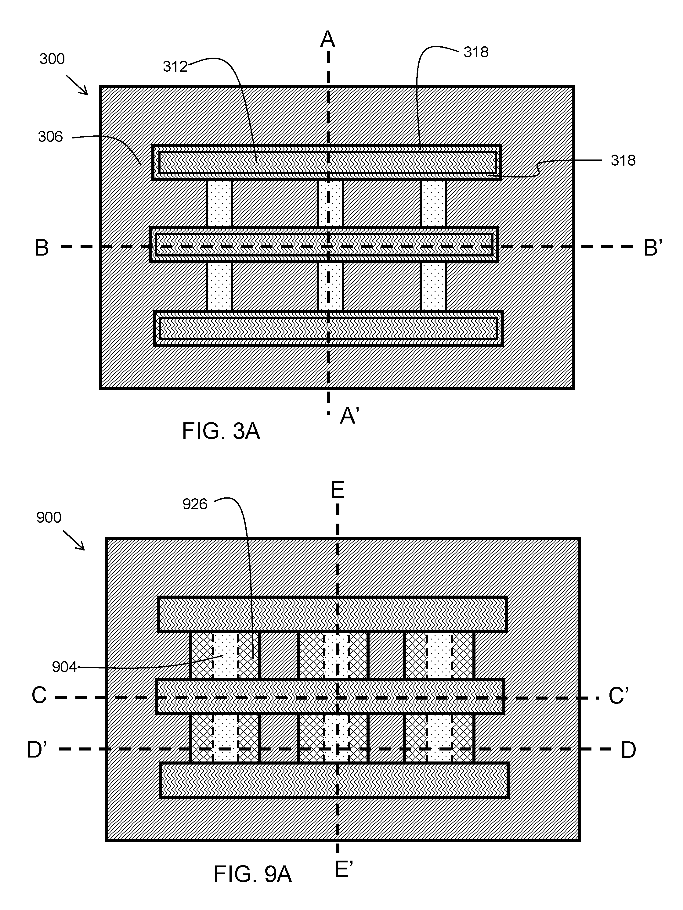
[0035] FIG. 3A is a top down view of a semiconductor structure 300 after a subsequent process step of forming gate spacers. In embodiments, the gate spacers 318 may be comprised of silicon nitride (SiN). FIG. 3B is a cross sectional view of the semiconductor structure of FIG. 3A as viewed along line A-A'. The spacers 318 extend to the top of fin 304, or to the top of the STI layer 306 in places where there is no fin.
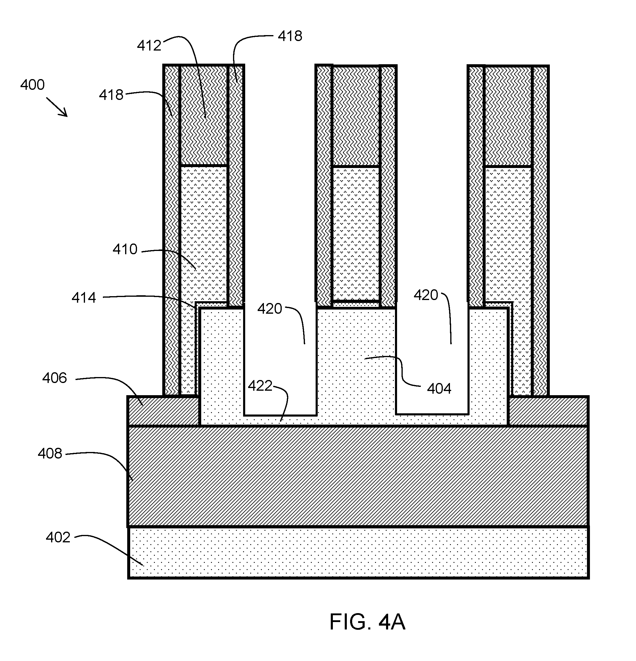
[0036] FIG. 4A is a cross sectional view of a semiconductor structure 400 (as viewed along line A-A' of FIG. 3A) after a subsequent process step of fin recess. The fin 404 is anisotropically recessed to form stressor cavities 420. In embodiments, the anisotropic recess is performed with a selective reactive ion etch process. The fin is not completely removed in the stressor cavities, such that a fin base 422 remains. FIG. 4B is a cross sectional view of semiconductor structure 400 as viewed along line B-B' of FIG. 3A after a subsequent process step of fin recess. As can be seen in this view, the recess is performed such that the top 423 of the fin base is below the top 407 of the STI layer 406.
[0037] FIG. 4C is a detailed view of a section of FIG. 4B as indicated by box 424. As can be seen in FIG. 4C, the fin base 422 has a depth D2. In embodiments, D2 may range from about 5 nanometers to about 20 nanometers. The stressor cavity 420 has a depth D3. In embodiments, the depth D3 may range from about 5 nanometers to about 20 nanometers. The depth D3 defines the thickness of the base portion of a tree shaped epitaxial region, as will be shown in upcoming figures.
[0038] FIG. 5A is a cross sectional view of semiconductor structure 500 as viewed along line A-A' of FIG. 3A after a subsequent process step of forming epitaxial regions 526. In embodiments, the epitaxial regions may comprise silicon, silicon germanium (SiGe), silicon carbon (SiC), or other suitable material. In some embodiments, the epitaxial regions 526 may be in-situ doped by a suitable dopant such as boron, phosphorus, or arsenic by adding a gas that contains the dopant species during the epitaxial growth. FIG. 5B is a cross sectional view of semiconductor structure 500 as viewed along line B-B' of FIG. 3A after a subsequent process step of forming epitaxial regions. As can be seen in this view, the epitaxial regions 526 form on the fin base 522 in a diamond shape once the height exceeds the top 507 of the STI layer 506, and the epitaxial region is no longer contained by the STI layer 506. The diamond shape is due to the properties of the crystalline planes of the epitaxial material. In embodiments, parameters of the epitaxial growth process such as temperature, pressure or the gas mixture are controlled so that the growth rate on the (111) crystallographic planes of the epitaxial regions 526 is significantly lower than the growth rate on other planes such as (100) and (110). For example, by adding a chlorine containing gas such as HCl during the epitaxy process, it is possible to reduce the growth rate on (111) crystallographic planes. FIG. 5C is a detailed view of a section of FIG. 5B as indicated by box 524 in FIG. 5B. As can be seen in FIG. 5C, epitaxial region 526 has a width D4. In embodiments, D4 may range from about 20 nanometers to about 50 nanometers. The epitaxial region 526 comprises a contained base portion 530 that is contained by the STI layer 506 to delay the formation of the diamond shape, and thus reduce the final width of the epitaxial region. The contained base portion 530 is disposed at a distance D2 (see FIG. 4C) from the bottom 505 of the fin. Outline 527 indicates a theoretical epitaxial shape that is grown without a contained fin base 522. That is, if the epitaxy starts growing uncontained, it ultimately reaches the diamond shape indicated by outline 527, and having a width D5, where D5>D4. Thus, the epitaxial region 526 is formed in a tree shape such that it has a base portion 530 that is substantially rectangular, with a diamond portion 531 disposed on the base portion 530. The diamond portion 531 is bounded by (111) crystalline planes. The epitaxial region 530 has the same height as the theoretical epitaxial shape indicated by outline 527, but has a reduced width, allowing for a reduced fin pitch that serves to increase circuit density while maintaining an increased current capacity for the finFET devices on an integrated circuit.
[0039] FIG. 6 is a cross sectional view of a semiconductor structure 600 as viewed along line A-A' of FIG. 3A after a subsequent process step of depositing an interlayer dielectric (ILD) 632. In embodiments, the ILD 632 may comprise silicon oxide, and may be deposited using a chemical vapor deposition (CVD) process. A planarization step may follow to make the top of the ILD 632 flush with the pad layer 612 and spacers 618. The bottom 617 of dummy gate structure 610 is in contact with shallow trench isolation layer 606.
[0040] FIG. 7A is a cross sectional view of a semiconductor structure 700 as viewed along line A-A' of FIG. 3A after a subsequent process step of removing the dummy gates (compare with 610 of FIG. 6). As a result of removing the dummy gates, gate cavities 734 are formed. At this stage, the dummy gate dielectric 714 remains at the bottom of the gate cavities 734. FIG. 7B is a cross sectional view of semiconductor structure 700 as viewed along line B-B' of FIG. 3A after a subsequent process step of removing the dummy gates. As part of the removal of the dummy gates, the spacers 718 are recessed to a level below the top of the ILD 732.
[0041] FIG. 8 is a cross sectional view of semiconductor structure 800 as viewed along line A-A' of FIG. 3A after a subsequent process step of removing the dummy gate dielectric (compare with 714 of FIG. 7A). In embodiments, the dummy gate dielectric is removed using an isotropic etch process that also etches a portion of the STI layer 806, such that the STI layer is now recessed below the bottom (see 617 of FIG. 6) of the dummy gate structures that were removed in a previous step. The etch is selective such that it does not substantially etch the spacers 818. Thus, a lower region 835 of the gate cavity 834 is formed. The lower region 835 of the gate cavity 834 extends below and directly underneath a portion of spacer 818.
[0042] FIG. 9A is a top down view of a semiconductor structure 900 after a subsequent process step of forming replacement metal gates. FIG. 9B is a cross sectional view of the semiconductor structure 900 of FIG. 9A as viewed along line E-E' after a subsequent process step of forming replacement metal gates. Note that the epitaxial regions 926 cover the tops of the fins 904. However, in FIG. 9A, the fins 904 are shown within the epitaxial regions 926 to illustrate the fin position within the epitaxial regions. The replacement metal gate (RMG) process may include deposition of a high-K gate dielectric 942. In embodiments, the high-K gate dielectric 942 may include hafnium oxide, hafnium silicate, or other suitable material. In embodiments, the high-K gate dielectric 942 is deposited using an atomic layer deposition (ALD) process. A replacement metal gate 940 is then formed in the gate cavity. The replacement metal gate 940 may include one or more barrier layers and work function metals (not shown) along with one or more fill metals. The gates are then capped with additional capping layer material 944. In embodiments, capping layer material 944 comprises silicon nitride. As can be seen in this view, due to the lower region 835 (see FIG. 8), the high-K dielectric 942 and a lower portion 940A of the replacement metal gate 940 are disposed below and directly underneath the spacer 918. Additionally, a portion of the STI layer 906 is disposed below, and directly underneath, and in direct physical contact with, the spacers 918. FIG. 9C is a cross sectional view of the semiconductor structure 900 as viewed along line C-C' of FIG. 9A. As can be seen in this view, along the gate edge, gate region 940B is disposed below and directly underneath spacers 918, as is a portion of the high-K dielectric layer 942. FIG. 9D is a cross sectional view of the semiconductor structure 900 as viewed along line D-D' of FIG. 9A. As can be seen in this view, epitaxial regions 926 are diamond shaped, and furthermore comprise a contained base portion 930 that is contained by the STI layer 906 to reduce the final width of the epitaxial region (as illustrated in FIG. 5C).
[0043] FIG. 10 is a cross sectional view of a semiconductor structure 1000 in accordance with an alternative embodiment, utilizing bulk fins 1022 that are formed from bulk substrate 1002. As stated previously, embodiments of the present invention may be utilized with both SOI and bulk finFET structures.
[0044] FIG. 11 is a flowchart 1100 indicating process steps for embodiments of the present invention. In process step 1150, fins are formed. In embodiments, this may comprise using a sidewall image transfer (SIT) process or other suitable technique. In process step 1152, an STI layer is formed (see 106 of FIG. 1B). This may comprise depositing silicon oxide using a chemical vapor deposition process, followed by a planarization process using a chemical mechanical polish. In process step 1154 a recess of the STI layer is performed. This may comprise using a selective reactive ion etch (RIE) process. In process step 1156, a dummy gate is formed (see 200 of FIG. 2A). This may include deposition of a dummy gate dielectric, followed by a dummy gate fill material and a capping layer. In process step 1158, spacers are formed (see 318 of FIG. 3B). In embodiments, this may include depositing a conformal silicon nitride layer, followed by an anisotropic etch process. In process step 1160, stressor cavities are formed (see 420 of FIG. 4A). The stressor cavities may be formed using an anisotropic etch process, such that a base portion of the fin remains at the bottom of the stressor cavity (see 422 of FIG. 4A). In process step 1162, epitaxial stressor regions are formed (see 526 of FIG. 5B). The epitaxial stressor regions comprise a contained base portion (see 530 of FIG. 5C) to delay the diamond shape growth and thus reduce the width of the epitaxial stressor regions. In process step 1164, the dummy gates are removed (see 800 of FIG. 8). In process step 1166, an RMG process is performed to form replacement metal gates (see 900 of FIG. 9C). From this point forward, industry-standard techniques may be used to complete the fabrication of the integrated circuit.
[0045] The corresponding structures, materials, acts, and equivalents of all means or step plus function elements in the claims, if applicable, are intended to include any structure, material, or act for performing the function in combination with other claimed elements as specifically claimed. The description of the present invention has been presented for purposes of illustration and description, but is not intended to be exhaustive or limited to the invention in the form disclosed. Many modifications and variations will be apparent to those of ordinary skill in the art without departing from the scope and spirit of the invention. The embodiment was chosen and described in order to best explain the principals of the invention and the practical application, and to enable others of ordinary skill in the art to understand the invention for various embodiments with various modifications as are suited to the particular use contemplated. Accordingly, while the invention has been described in terms of embodiments, those of skill in the art will recognize that the invention can be practiced with modifications and in the spirit and scope of the appended claims, and advantageous for any given or particular application.
* * * * *
D00000
D00001
D00002
D00003
D00004
D00005
D00006
D00007
D00008
D00009
D00010
D00011
D00012

D00013

D00014

D00015

D00016

D00017

D00018

XML
uspto.report is an independent third-party trademark research tool that is not affiliated, endorsed, or sponsored by the United States Patent and Trademark Office (USPTO) or any other governmental organization. The information provided by uspto.report is based on publicly available data at the time of writing and is intended for informational purposes only.
While we strive to provide accurate and up-to-date information, we do not guarantee the accuracy, completeness, reliability, or suitability of the information displayed on this site. The use of this site is at your own risk. Any reliance you place on such information is therefore strictly at your own risk.
All official trademark data, including owner information, should be verified by visiting the official USPTO website at www.uspto.gov. This site is not intended to replace professional legal advice and should not be used as a substitute for consulting with a legal professional who is knowledgeable about trademark law.