Semiconductor module
Kanda , et al. Ja
U.S. patent number D873,226 [Application Number D/666,187] was granted by the patent office on 2020-01-21 for semiconductor module. This patent grant is currently assigned to ROHM CO., LTD.. The grantee listed for this patent is ROHM CO., LTD.. Invention is credited to Masashi Hayashiguchi, Takumi Kanda.


View All Diagrams
| United States Patent | D873,226 |
| Kanda , et al. | January 21, 2020 |
Semiconductor module
Claims
CLAIM The ornamental design for a semiconductor module, as shown and described.
| Inventors: | Kanda; Takumi (Kyoto, JP), Hayashiguchi; Masashi (Kyoto, JP) | ||||||||||
|---|---|---|---|---|---|---|---|---|---|---|---|
| Applicant: |
|
||||||||||
| Assignee: | ROHM CO., LTD. (Kyoto,
JP) |
||||||||||
| Appl. No.: | D/666,187 | ||||||||||
| Filed: | October 10, 2018 |
Foreign Application Priority Data
| Apr 13, 2018 [JP] | 2018-008228 | |||
| Apr 13, 2018 [JP] | 2018-008232 | |||
| Current U.S. Class: | D13/182 |
| Current International Class: | 1303 |
| Field of Search: | ;D13/182 |
References Cited [Referenced By]
U.S. Patent Documents
| D394244 | May 1998 | Majumdar |
| D401912 | December 1998 | Majumdar |
| D448739 | October 2001 | Iwasaki |
| D505399 | May 2005 | Yoshida |
| D606951 | December 2009 | Soyano |
| D705184 | May 2014 | Takahashi |
| D717253 | November 2014 | Jo |
| D717254 | November 2014 | Jo |
| D717255 | November 2014 | Lim |
| D717256 | November 2014 | Sohn |
| D719113 | December 2014 | Sohn |
| D719537 | December 2014 | Kawase |
| D719926 | December 2014 | Sohn |
| 1145764 | Jul 2002 | JP | |||
| 1146361 | Jul 2002 | JP | |||
| 1146362 | Jul 2002 | JP | |||
| 1146363 | Jul 2002 | JP | |||
| 1305812 | Jul 2007 | JP | |||
| 1551590 | Jun 2016 | JP | |||
| 1565636 | Dec 2016 | JP | |||
| 1578687 | Jun 2017 | JP | |||
Attorney, Agent or Firm: Hamre, Schumann, Mueller & Larson, P.C.
Description
FIG. 1 is a front, top and right side perspective view of a first embodiment of a semiconductor module showing our new design;
FIG. 2 is a rear, bottom, and left side perspective view thereof;
FIG. 3 is a front view, the rear view being identical to FIG. 3;
FIG. 4 is a top plan view thereof;
FIG. 5 is a bottom plan view thereof;
FIG. 6 is a right side view thereof;
FIG. 7 is a left side view thereof;
FIG. 8 is a cross-sectional view taken along line 8-8 in FIG. 4;
FIG. 9 is a cross-sectional view taken along line 9-9 in FIG. 4;
FIG. 10 is a front, top and right side perspective view of a second embodiment of a semiconductor module showing our new design;
FIG. 11 is a rear, bottom, and left side perspective view thereof;
FIG. 12 is a front view, the rear view being identical to FIG. 12;
FIG. 13 is a top plan view thereof;
FIG. 14 is a bottom plan view thereof;
FIG. 15 is a right side view thereof;
FIG. 16 is a left side view thereof;
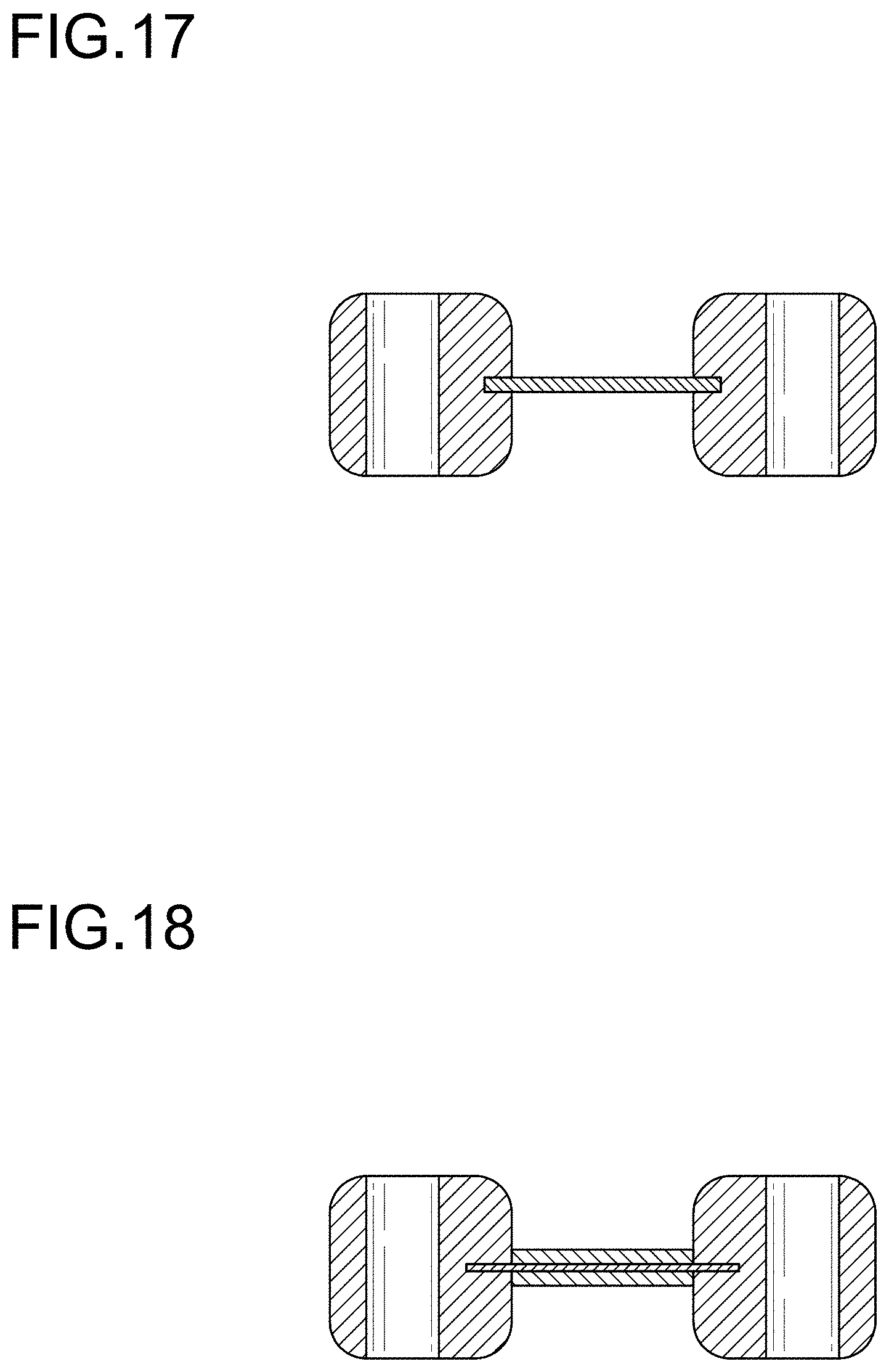
FIG. 17 is a cross-sectional view taken along line 17-17 in FIG. 13; and,
FIG. 18 is a cross-sectional view taken along line 18-18 in FIG. 13.
The member illustrated with fine, diagonal, parallel lines in FIG. 2 and FIG. 5 is translucent.
* * * * *
D00000
D00001
D00002
D00003
D00004
D00005
D00006
D00007
D00008
D00009
D00010
D00011
D00012

D00013

D00014
XML
uspto.report is an independent third-party trademark research tool that is not affiliated, endorsed, or sponsored by the United States Patent and Trademark Office (USPTO) or any other governmental organization. The information provided by uspto.report is based on publicly available data at the time of writing and is intended for informational purposes only.
While we strive to provide accurate and up-to-date information, we do not guarantee the accuracy, completeness, reliability, or suitability of the information displayed on this site. The use of this site is at your own risk. Any reliance you place on such information is therefore strictly at your own risk.
All official trademark data, including owner information, should be verified by visiting the official USPTO website at www.uspto.gov. This site is not intended to replace professional legal advice and should not be used as a substitute for consulting with a legal professional who is knowledgeable about trademark law.