Peripheral component interconnect card panel
Morgan , et al. Nov
U.S. patent number D866,560 [Application Number D/633,235] was granted by the patent office on 2019-11-12 for peripheral component interconnect card panel. This patent grant is currently assigned to Intel Corporation. The grantee listed for this patent is Intel Corporation. Invention is credited to Michael Hyde, Duck Young Kong, Aleksander Magi, Wesley Brook Morgan.


| United States Patent | D866,560 |
| Morgan , et al. | November 12, 2019 |
Peripheral component interconnect card panel
Claims
CLAIM The ornamental design for a peripheral component interconnect card panel, as shown and described in FIGS. 1-7.
| Inventors: | Morgan; Wesley Brook (Olympia, WA), Magi; Aleksander (Portland, OR), Kong; Duck Young (Beaverton, OR), Hyde; Michael (San Francisco, CA) | ||||||||||
|---|---|---|---|---|---|---|---|---|---|---|---|
| Applicant: |
|
||||||||||
| Assignee: | Intel Corporation (Santa Clara,
CA) |
||||||||||
| Appl. No.: | D/633,235 | ||||||||||
| Filed: | January 12, 2018 |
| Current U.S. Class: | D14/436 |
| Current International Class: | 1402 |
| Field of Search: | ;D14/356,357,358,432,433,434,435,435.1,436,437,300,301,313,257,388,454 ;D13/123,133,139.1,139.3,139.4,154,173,184 ;D8/349,364,366,381,404,499 ;D25/35,55,58,60 |
References Cited [Referenced By]
U.S. Patent Documents
| D299139 | December 1988 | Toft |
| D322780 | December 1991 | Wislocki |
| D340043 | October 1993 | Louis |
| D360419 | July 1995 | Weber |
| D364398 | November 1995 | Lam |
| D371134 | June 1996 | Brosowske |
| D372909 | August 1996 | Naufel |
| D397107 | August 1998 | Klinker |
| D398004 | September 1998 | Klinker |
| D398592 | September 1998 | Klinker |
| D399502 | October 1998 | Klinker |
| D405437 | February 1999 | Klinker |
| D405440 | February 1999 | Klinker |
| D405772 | February 1999 | Klinker |
| D405778 | February 1999 | Klinker |
| D409178 | May 1999 | Klinker |
| D413109 | August 1999 | Klinker |
| D413315 | August 1999 | Klinker |
| D413316 | August 1999 | Klinker |
| 6021049 | February 2000 | Thompson |
| D436357 | January 2001 | Klinker |
| D457887 | May 2002 | Kadonaga |
| D458935 | June 2002 | Hiroki |
| D469771 | February 2003 | Nishio |
| D469772 | February 2003 | Nishio |
| D489725 | May 2004 | Hu |
| D492688 | July 2004 | Wallace |
| D493799 | August 2004 | Chiang |
| D498760 | November 2004 | Chiang |
| D505959 | June 2005 | Yamada |
| D507795 | July 2005 | Yamada |
| D510579 | October 2005 | Yamada |
| D510935 | October 2005 | Yamada |
| D520015 | May 2006 | Peddle |
| D523435 | June 2006 | Takiar |
| D523857 | June 2006 | Nakamura |
| D524314 | July 2006 | Nakamura |
| D525248 | July 2006 | Takiar |
| D525623 | July 2006 | Takiar |
| D525978 | August 2006 | Takiar |
| D530331 | October 2006 | Yao |
| D533556 | December 2006 | Yamada |
| D537081 | February 2007 | Takiar |
| D538286 | March 2007 | Takiar |
| D552613 | October 2007 | Tan |
| D555653 | November 2007 | Tseng |
| D558210 | December 2007 | Tseng |
| D574376 | August 2008 | Park |
| D591753 | May 2009 | Nakano |
| D591754 | May 2009 | Hwangbo |
| D607885 | January 2010 | Otani |
| D611945 | March 2010 | Yao |
| D618680 | June 2010 | Marchand |
| D620455 | July 2010 | Teixeira Pinto Dias |
| D623178 | September 2010 | Lu |
| D628202 | November 2010 | Pomerantz |
| D638431 | May 2011 | Pomerantz |
| D673144 | December 2012 | Onoue |
| D690676 | October 2013 | Daniel |
| D702692 | April 2014 | Gallagher |
| D730907 | June 2015 | Lim |
| D735726 | August 2015 | Chen |
| D745523 | December 2015 | Magi |
| D748627 | February 2016 | Russette |
| D748638 | February 2016 | Russette |
| D753090 | April 2016 | Langhammer |
| D755182 | May 2016 | Bassett |
| D773468 | December 2016 | Ellis, II |
| 9600040 | March 2017 | Han |
| D850448 | June 2019 | Lewis |
| 2005/0213300 | September 2005 | Tran |
| 2010/0061046 | March 2010 | Huang |
| 2010/0172079 | July 2010 | Wu |
| 2014/0293567 | October 2014 | Kuo |
| 2016/0335140 | November 2016 | Liu |
| 2018/0138612 | May 2018 | Lin |
| 2019/0227605 | July 2019 | Wiltzius |
Attorney, Agent or Firm: Hanley, Flight and Zimmerman, LLC
Description
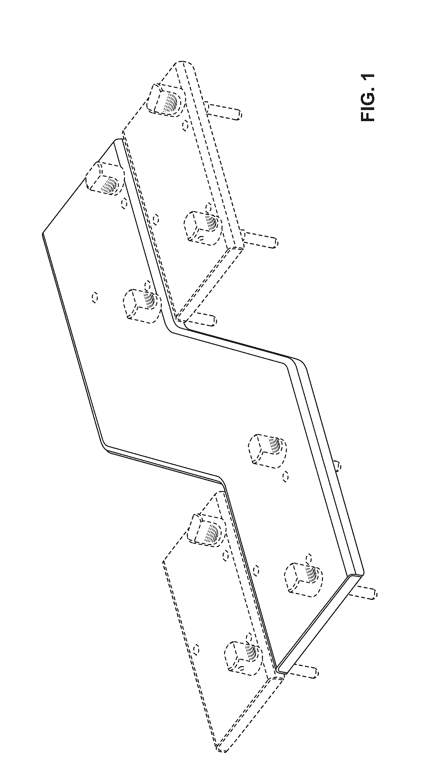
FIG. 1 is a right, front, top perspective view of a peripheral component interconnect card panel.
FIG. 2 is a top view of the PCI card panel of FIG. 1.
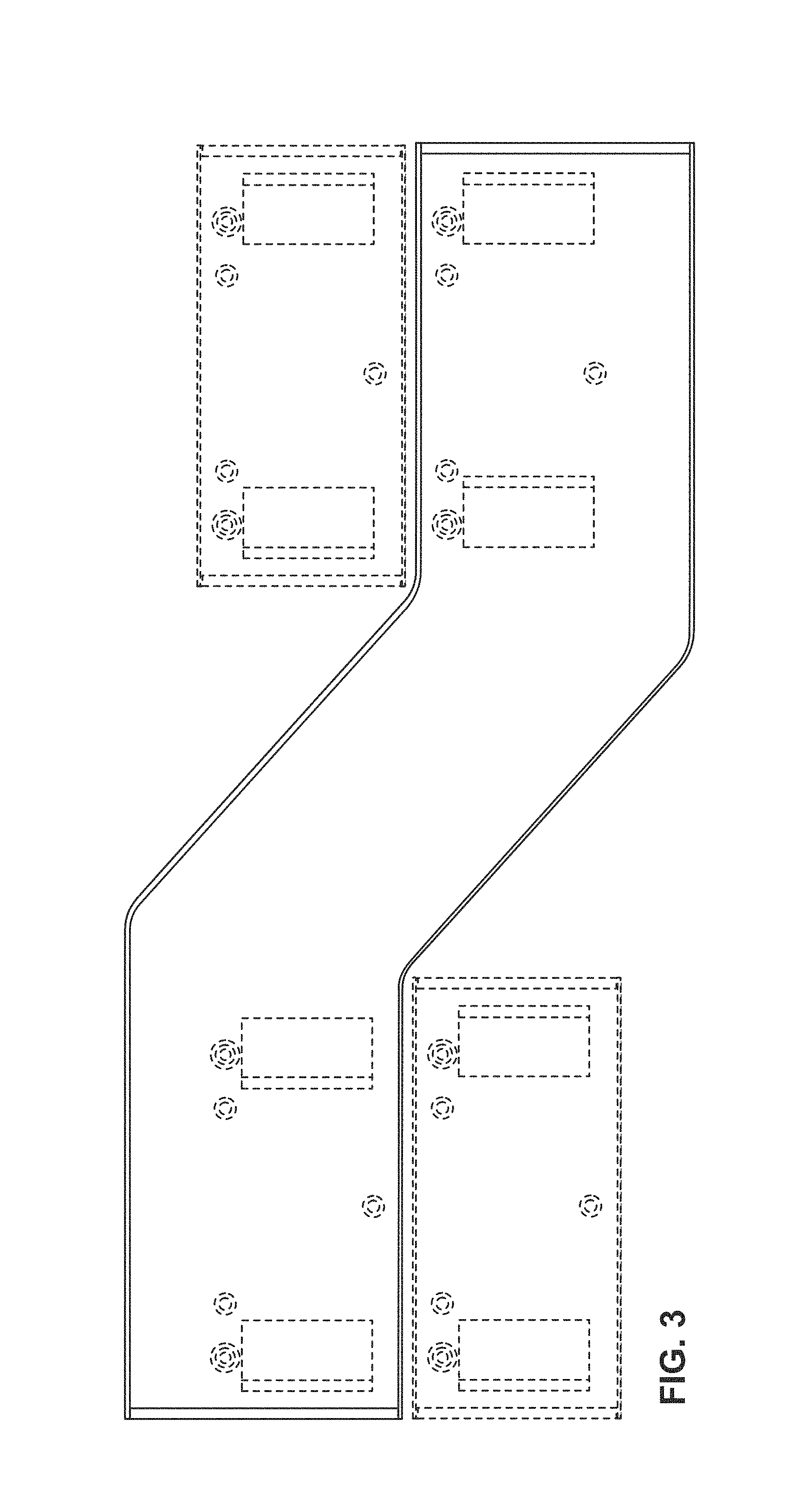
FIG. 3 is a bottom view of the PCI card panel of FIG. 1.
FIG. 4 is an enlarged front view of the PCI card panel of FIG. 1.
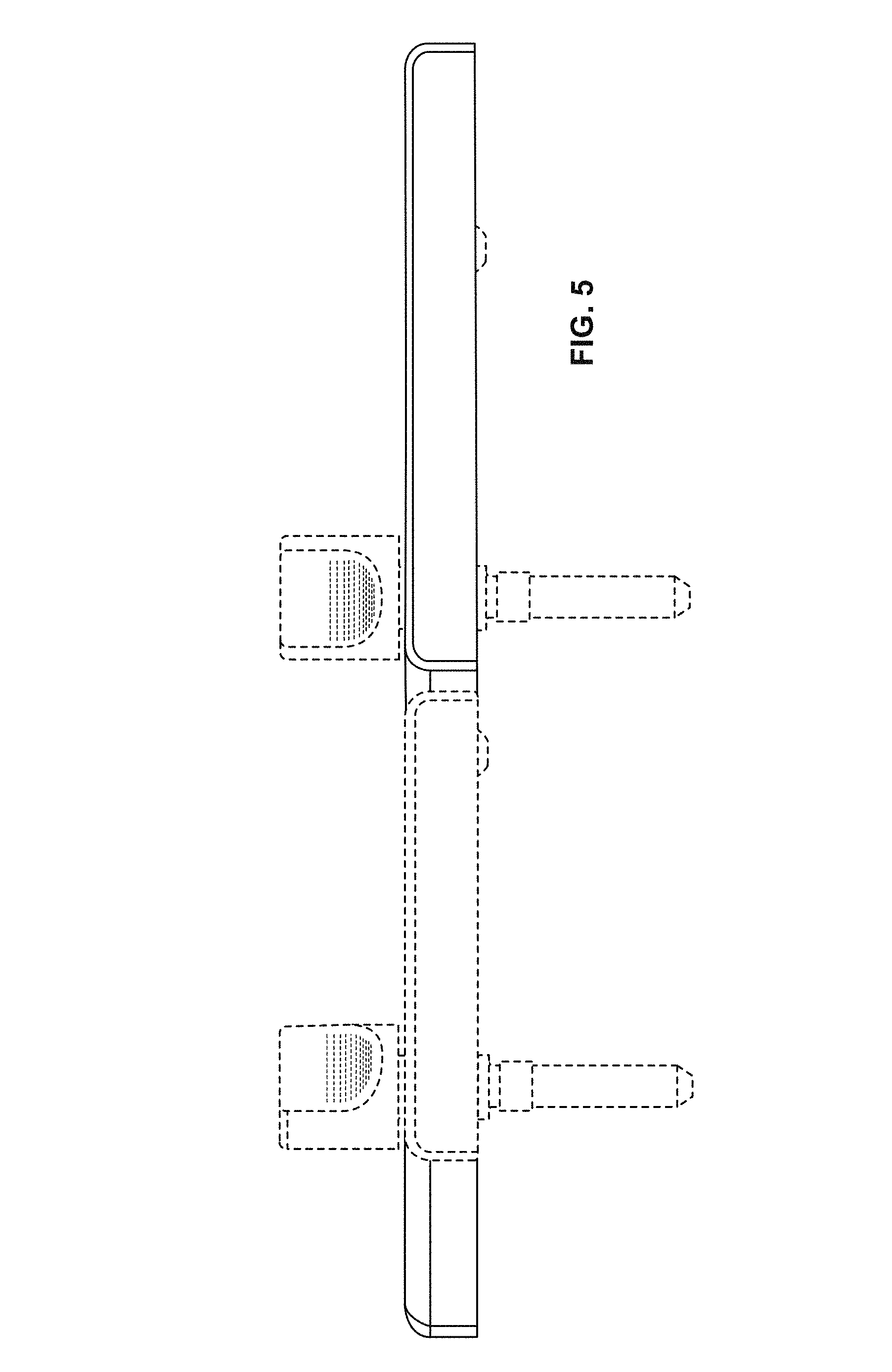
FIG. 5 is an enlarged rear view of the PCI card panel of FIG. 1.
FIG. 6 is a left side view of the PCI card panel of FIG. 1; and,
FIG. 7 is a right side view of the PCI card panel of FIG. 1.
The broken lines in the drawings depict portions of the PCI card panel that form no part of the claimed design.
* * * * *
D00000
D00001
D00002
D00003
D00004
D00005
D00006
D00007
XML
uspto.report is an independent third-party trademark research tool that is not affiliated, endorsed, or sponsored by the United States Patent and Trademark Office (USPTO) or any other governmental organization. The information provided by uspto.report is based on publicly available data at the time of writing and is intended for informational purposes only.
While we strive to provide accurate and up-to-date information, we do not guarantee the accuracy, completeness, reliability, or suitability of the information displayed on this site. The use of this site is at your own risk. Any reliance you place on such information is therefore strictly at your own risk.
All official trademark data, including owner information, should be verified by visiting the official USPTO website at www.uspto.gov. This site is not intended to replace professional legal advice and should not be used as a substitute for consulting with a legal professional who is knowledgeable about trademark law.