Chemical vapor deposition wafer carrier with thermal cover
Krishnan , et al. Oc
U.S. patent number D863,239 [Application Number D/641,931] was granted by the patent office on 2019-10-15 for chemical vapor deposition wafer carrier with thermal cover. This patent grant is currently assigned to Veeco Instruments Inc.. The grantee listed for this patent is Veeco Instruments Inc.. Invention is credited to Leo Chin, Mandar Deshpande, Alexander Gurary, Sandeep Krishnan, Yuliy Rashkovsky.


| United States Patent | D863,239 |
| Krishnan , et al. | October 15, 2019 |
Chemical vapor deposition wafer carrier with thermal cover
Claims
CLAIM The ornamental design for a chemical vapor deposition wafer carrier with thermal cover, as shown and described.
| Inventors: | Krishnan; Sandeep (Jersey City, NJ), Rashkovsky; Yuliy (Millburn, NJ), Gurary; Alexander (Bridgewater, NJ), Chin; Leo (Poughquag, NY), Deshpande; Mandar (Bridgewater, NJ) | ||||||||||
|---|---|---|---|---|---|---|---|---|---|---|---|
| Applicant: |
|
||||||||||
| Assignee: | Veeco Instruments Inc.
(Plainview, NY) |
||||||||||
| Appl. No.: | D/641,931 | ||||||||||
| Filed: | March 26, 2018 |
| Current U.S. Class: | D13/182 |
| Current International Class: | 1303 |
| Field of Search: | ;D13/182 ;D15/144,144.1,144.2 ;D23/323,328,335,336,337,341,352,357,385,386,397,399,400,406,411,413,499 |
References Cited [Referenced By]
U.S. Patent Documents
| 3461537 | August 1969 | Lotz |
| 3783822 | January 1974 | Wollam |
| 3845738 | November 1974 | Berkman et al. |
| 3895967 | July 1975 | Anthony et al. |
| 4165584 | August 1979 | Scherrer |
| D320361 | October 1991 | Karasawa |
| D325934 | May 1992 | Ramljak |
| 5152842 | October 1992 | Urata et al. |
| 5191738 | March 1993 | Nakazato |
| 5242501 | September 1993 | McDiarmid |
| 5690742 | November 1997 | Ogata et al. |
| 6001183 | December 1999 | Gurary et al. |
| 6436796 | August 2002 | Mailho et al. |
| 6492625 | December 2002 | Boguslayskiy et al. |
| 6506252 | January 2003 | Boguslayskiy et al. |
| 6666756 | December 2003 | Travis |
| 6902623 | June 2005 | Gurary et al. |
| D517073 | March 2006 | McDonald et al. |
| 7101272 | September 2006 | Chen et al. |
| 7122844 | October 2006 | Nakamura et al. |
| 7276124 | October 2007 | Gurary et al. |
| 8021487 | September 2011 | Boguslayskiy et al. |
| 8092599 | January 2012 | Sferlazzo et al. |
| 8093696 | January 2012 | Yoon et al. |
| 8182315 | May 2012 | Nguyen |
| 8216379 | July 2012 | Ishikawa |
| D674759 | January 2013 | Chang |
| 8366830 | February 2013 | Nakamura et al. |
| 8367477 | February 2013 | Chien et al. |
| 8372204 | February 2013 | Nakamura et al. |
| D686175 | July 2013 | Gurary |
| D686582 | July 2013 | Krishnan |
| 8486726 | July 2013 | Mangum et al. |
| 8518753 | August 2013 | Wu et al. |
| 8535445 | September 2013 | Volf et al. |
| D690671 | October 2013 | Gurary |
| 8552547 | October 2013 | Chien et al. |
| 8562746 | October 2013 | Gurary et al. |
| D695241 | December 2013 | Gurary |
| D695242 | December 2013 | Gurary |
| 8603248 | December 2013 | Gurary et al. |
| D704155 | May 2014 | Chang |
| D721417 | January 2015 | Sawchuk |
| 9017483 | April 2015 | Fujikawa et al. |
| D731409 | June 2015 | Erlich et al. |
| D754785 | April 2016 | Gibson |
| D778247 | February 2017 | Gurary |
| D793971 | August 2017 | Krishnan |
| D793972 | August 2017 | Krishnan |
| D797067 | September 2017 | Zhang |
| D806046 | December 2017 | Gurary |
| D813181 | March 2018 | Okajima |
| 2002/0027762 | March 2002 | Yamaguchi |
| 2003/0057089 | March 2003 | Nguyen |
| 2004/0179323 | September 2004 | Litman et al. |
| 2005/0011436 | January 2005 | Liu |
| 2005/0274374 | December 2005 | Boguslayskiy et al. |
| 2006/0102081 | May 2006 | Ueno et al. |
| 2007/0186853 | August 2007 | Gurary et al. |
| 2009/0155028 | June 2009 | Boguslavskiy |
| 2009/0224175 | September 2009 | Lee et al. |
| 2010/0055318 | March 2010 | Volf et al. |
| 2010/0055320 | March 2010 | Honma |
| 2010/0162957 | July 2010 | Boyd et al. |
| 2010/0190418 | July 2010 | Yasuoka et al. |
| 2011/0049779 | March 2011 | Egami et al. |
| 2011/0290175 | December 2011 | Paranjpe et al. |
| 2011/0300297 | December 2011 | Celaru et al. |
| 2012/0040097 | February 2012 | Volf et al. |
| 2012/0156374 | June 2012 | Gurary et al. |
| 2012/0234229 | September 2012 | Nguyen et al. |
| 2012/0240859 | September 2012 | Chen |
| 2012/0272892 | November 2012 | Paranjpe et al. |
| 2013/0175005 | July 2013 | Gowdaru et al. |
| 2013/0276704 | October 2013 | Krishnan |
| 2013/0291798 | November 2013 | Lee et al. |
| 2014/0110894 | April 2014 | Lee et al. |
| 2014/0261187 | September 2014 | Krishnan et al. |
| 2014/0261698 | September 2014 | Krishnan |
| 2014/0360430 | December 2014 | Armour |
| 2015/0118009 | April 2015 | Hsieh |
| 2015/0187620 | July 2015 | Gurary et al. |
| 2015/0330601 | November 2015 | Jungwirth |
| 2016/0251758 | September 2016 | Mitrovic et al. |
| 2017/0076972 | March 2017 | Krishnan |
| 2017/0121847 | May 2017 | Armour et al. |
| 102130035 | Jul 2011 | CN | |||
| 202492576 | Oct 2012 | CN | |||
| 103258763 | Aug 2013 | CN | |||
| 203569185 | Apr 2014 | CN | |||
| 203569186 | Apr 2014 | CN | |||
| 203715721 | Jul 2014 | CN | |||
| 204982132 | Jan 2016 | CN | |||
| 105369348 | Mar 2016 | CN | |||
| 105810625 | Jul 2016 | CN | |||
| 105810626 | Jul 2016 | CN | |||
| 206127421 | Apr 2017 | CN | |||
| 10261362 | Jul 2004 | DE | |||
| 0795624 | Sep 1997 | EP | |||
| 1096549 | May 2001 | EP | |||
| S58128724 | Aug 1983 | JP | |||
| H04110466 | Apr 1992 | JP | |||
| H10167885 | Jun 1998 | JP | |||
| H10167886 | Jun 1998 | JP | |||
| 2004128271 | Apr 2004 | JP | |||
| 2006066417 | Mar 2006 | JP | |||
| 5156240 | Mar 2013 | JP | |||
| 100854974 | Aug 2008 | KR | |||
| 1020090036722 | Apr 2009 | KR | |||
| 1020090038606 | Apr 2009 | KR | |||
| 101235928 | Feb 2013 | KR | |||
| D142257 | Sep 2011 | TW | |||
| D152296 | Mar 2013 | TW | |||
| M496228 | Feb 2015 | TW | |||
| 201624596 | Jul 2016 | TW | |||
| 201624605 | Jul 2016 | TW | |||
| M531049 | Oct 2016 | TW | |||
| D181305 | Feb 2017 | TW | |||
| D181306 | Feb 2017 | TW | |||
| WO 1999/018599 | Apr 1999 | WO | |||
| WO 2003/069029 | Aug 2003 | WO | |||
| WO 2012/021370 | Feb 2012 | WO | |||
| WO 2013/123859 | Aug 2013 | WO | |||
Other References
|
Gurary et al., "Investigation of the Wafer Temperature Uniformity in an OMVPE Vertical Rotating Disk Reactor," Journal of Electronic Material, Nov. 1995, vol. 24, Issue 11, Abstract, 1 page. cited by applicant . International Written Opinion and Search Report for International Application No. PCT/US2011/061615 dated May 18, 2012, 9 pages. cited by applicant . Application No. PCT/US2014/072425, filed Dec. 26, 2014, International Search Report dated Apr. 29, 2015, 3 pages. cited by applicant . Application No. PCT/US2014/072425, filed Dec. 26, 2014, Written Opinion dated Apr. 29, 2015, 7 pages. cited by applicant . Application No. PCT/US2011/0456567, Search Report dated Dec. 21, 2011, 6 pages. cited by applicant . Application No. PCT/US2014/041134, Written Opinion and Search Report dated Oct. 7, 2014, 11 pages. cited by applicant . Taiwan Application No. 103145394, Search Report dated Jan. 9, 2018, 9 page. cited by applicant . Taiwan Application No. 106307693, Office Action dated Jun. 8, 2018, 2 pages. cited by applicant . Taiwan Application No. 106307693D01, Search Report dated May 5, 2018, 1 page. cited by applicant . Application and file history for U.S. Appl. No. 14/297,244, filed Jun. 5, 2014. Inventors: Armour et al. cited by applicant . Application and file history for U.S. Appl. No. 15/403,709, filed Jan. 11, 2017. Inventors: Armour et al. cited by applicant . Application and file history for U.S. Appl. No. 14/583,346, filed Dec. 26, 2014. Inventors: Guruary et al. cited by applicant . Application and file history for Design U.S. Appl. No. 29/641,924, filed Mar. 26, 2018. Inventors: Krishnan et al. cited by applicant . Application and file history for Design U.S. Appl. No. 29/627,938, filed Nov. 30, 2017. Inventors: Rashkovsky et al. cited by applicant . Application and file history for Design U.S. Appl. No. 29/627,940, filed Nov. 30, 2017. Inventors: Rashkovsky et al. cited by applicant . Application and file history for Design U.S. Appl. No. 29/641,925, filed Mar. 26, 2018. Inventors Krishnan et al. cited by applicant . Application and file history for Design U.S. Appl. No. 29/641,927, filed Mar. 26, 2018. Inventors: Krishnan et al. cited by applicant . Application and file history for Design U.S. Appl. No. 29/641,928, filed Mar. 16, 2018. Inventors: Krishnan et al. cited by applicant . Application and file history for Design U.S. Appl. No. 29/641,930, filed Mar. 26, 2018. Inventors: Krishnan et al. cited by applicant . Application and file history for Design U.S. Appl. No. 29/641,933, filed Mar. 26, 2018. Inventors: Krishnan et al. cited by applicant. |
Primary Examiner: Oswecki; Elizabeth J
Attorney, Agent or Firm: Patterson Thuente Pedersen, P.A.
Description
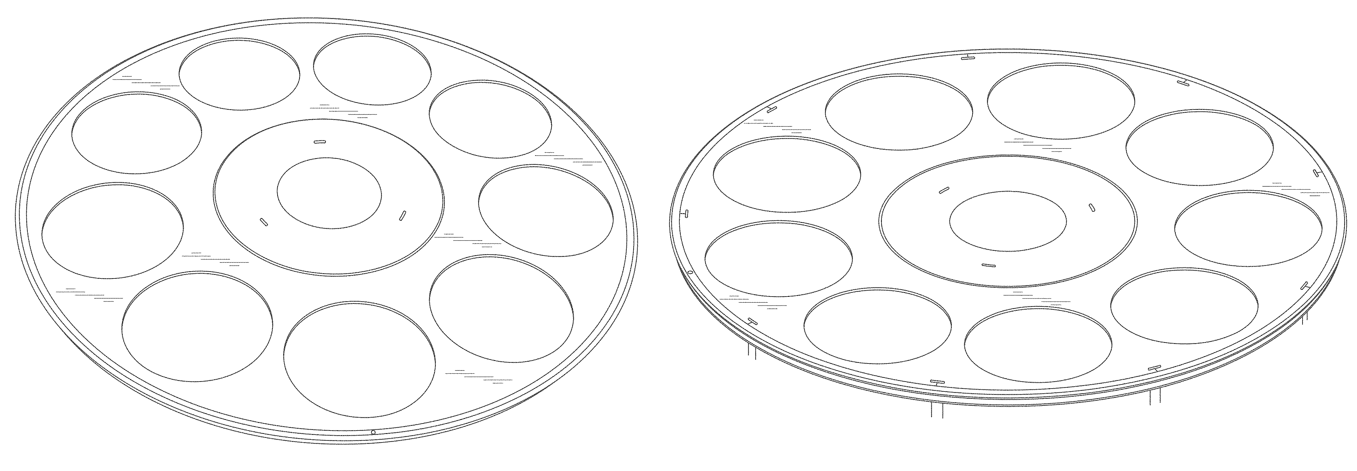
FIG. 1 is a perspective view of a first embodiment of a chemical vapor deposition wafer carrier with thermal cover showing our new design.
FIG. 2 is a top plan view thereof.
FIG. 3 is a right side view thereof, with the left side view, front view, and rear view being identical.
FIG. 4 is a bottom plan view thereof.
FIG. 5 is a perspective view of a second embodiment of a chemical vapor deposition wafer carrier with thermal cover, showing our new design, which differs from the embodiment shown in FIG. 1 in that it includes staples extending through the thickness of the chemical vapor deposition wafer carrier with thermal cover; and,
FIG. 6 is a perspective view of the thermal cover of the chemical vapor deposition wafer carrier with thermal cover, shown separately from the base without staples for ease of illustration.
In each of the figures, portions or features shown in broken lines form no part of the claimed design.
* * * * *
D00000
D00001
D00002
D00003
D00004
D00005
D00006
XML
uspto.report is an independent third-party trademark research tool that is not affiliated, endorsed, or sponsored by the United States Patent and Trademark Office (USPTO) or any other governmental organization. The information provided by uspto.report is based on publicly available data at the time of writing and is intended for informational purposes only.
While we strive to provide accurate and up-to-date information, we do not guarantee the accuracy, completeness, reliability, or suitability of the information displayed on this site. The use of this site is at your own risk. Any reliance you place on such information is therefore strictly at your own risk.
All official trademark data, including owner information, should be verified by visiting the official USPTO website at www.uspto.gov. This site is not intended to replace professional legal advice and should not be used as a substitute for consulting with a legal professional who is knowledgeable about trademark law.