Electrode cover for a plasma processing apparatus
Ichino , et al. Feb
U.S. patent number D840,364 [Application Number D/610,996] was granted by the patent office on 2019-02-12 for electrode cover for a plasma processing apparatus. This patent grant is currently assigned to Hitachi High-Technologies Corporation. The grantee listed for this patent is Hitachi High-Technologies Corporation. Invention is credited to Takamasa Ichino, Kazunori Nakamoto, Kohei Sato.


| United States Patent | D840,364 |
| Ichino , et al. | February 12, 2019 |
Electrode cover for a plasma processing apparatus
Claims
CLAIM The ornamental design for an electrode cover for a plasma processing apparatus, as shown and described.
| Inventors: | Ichino; Takamasa (Tokyo, JP), Sato; Kohei (Tokyo, JP), Nakamoto; Kazunori (Tokyo, JP) | ||||||||||
|---|---|---|---|---|---|---|---|---|---|---|---|
| Applicant: |
|
||||||||||
| Assignee: | Hitachi High-Technologies
Corporation (Tokyo, JP) |
||||||||||
| Appl. No.: | D/610,996 | ||||||||||
| Filed: | July 18, 2017 |
Foreign Application Priority Data
| Jan 31, 2017 [JP] | 2017-001753 | |||
| Current U.S. Class: | D13/182 |
| Current International Class: | 1303 |
| Field of Search: | ;D13/158-177,182,184 ;204/286.1,297.1 ;205/118,123 ;200/1R,5R,52R,315,310,6A,302.1,308,314,317,11R,16B |
References Cited [Referenced By]
U.S. Patent Documents
| D404372 | January 1999 | Ishii |
| D494551 | August 2004 | Doba |
| D557226 | December 2007 | Uchino et al. |
| D557425 | December 2007 | Nakamura et al. |
| D559993 | January 2008 | Nagakubo |
| D559994 | January 2008 | Nagakubo et al. |
| D699199 | February 2014 | Kuwabara |
| D699200 | February 2014 | Nagakubo |
| D709536 | July 2014 | Yoshimura |
| D709537 | July 2014 | Kuwabara |
| D709538 | July 2014 | Mizukami |
| D709539 | July 2014 | Kuwabara |
| D717746 | November 2014 | Lau |
| D729730 | May 2015 | Gillespie-Brown |
| D770992 | November 2016 | Tauchi et al. |
| D783922 | April 2017 | Kirkland |
| D789888 | June 2017 | Jang |
| D797691 | September 2017 | Joubert |
| D803917 | November 2017 | Harada |
| D804556 | December 2017 | Harada |
| D810705 | February 2018 | Krishnan |
| D813181 | March 2018 | Okajima |
| 2004/0077167 | April 2004 | Willis |
| 2009/0050272 | February 2009 | Rosenberg |
| 2012/0263569 | October 2012 | Priddy |
| 2015/0024330 | January 2015 | Tian |
| 2016/0002788 | January 2016 | Nal |
| D1210213 | Jun 2004 | JP | |||
| D1361441 | Jun 2009 | JP | |||
| D1551512 | Jun 2014 | JP | |||
Other References
|
Ichino et al., Design U.S. Appl. No. 29/610,995, filed Jul. 18, 2017. cited by applicant . Ichino et al., Design U.S. Appl. No. 29/610,998, filed Jul. 18, 2017. cited by applicant . Ichino et al., Design U.S. Appl. No. 29/610,999, filed Jul. 18, 2017. cited by applicant . Nunomura et al., Design U.S. Appl. No. 29/611,001, filed Jul. 18, 2017. cited by applicant. |
Primary Examiner: Oswecki; Elizabeth J
Attorney, Agent or Firm: Crowell & Moring LLP
Description
This application contains subject matter related to the following co-pending U.S. design patent applications:
Application Ser. No. 29/610,995, filed herewith and entitled "Electrode Cover for a Plasma Processing Apparatus";
Application Ser. No. 29/610,998, filed herewith and entitled "Ring for a Plasma Processing Apparatus";
Application Ser. No. 29/610,999, filed herewith and entitled "Cover Ring for a Plasma Processing Apparatus"; and
Application Ser. No. 29/611,001, filed herewith and entitled "Discharge Chamber for a Plasma Processing Apparatus".
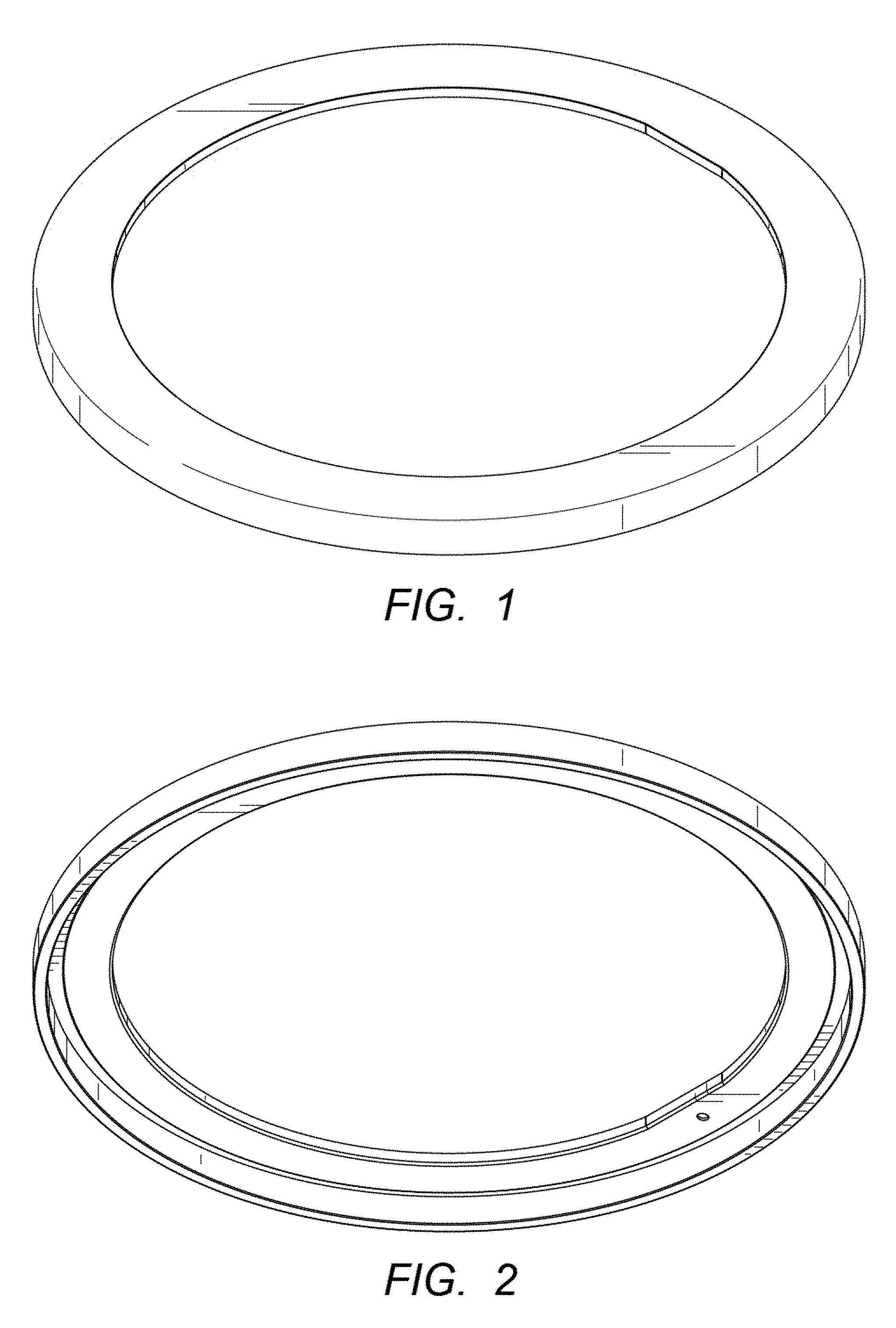
FIG. 1 is a front, top and right side perspective view of an electrode cover for a plasma processing apparatus, showing our new design;
FIG. 2 is a front, bottom and right side perspective view thereof;
FIG. 3 is a front elevational view thereof;
FIG. 4 is a rear elevational view thereof;
FIG. 5 is a right side elevational view thereof;
FIG. 6 is a left side elevational view thereof;
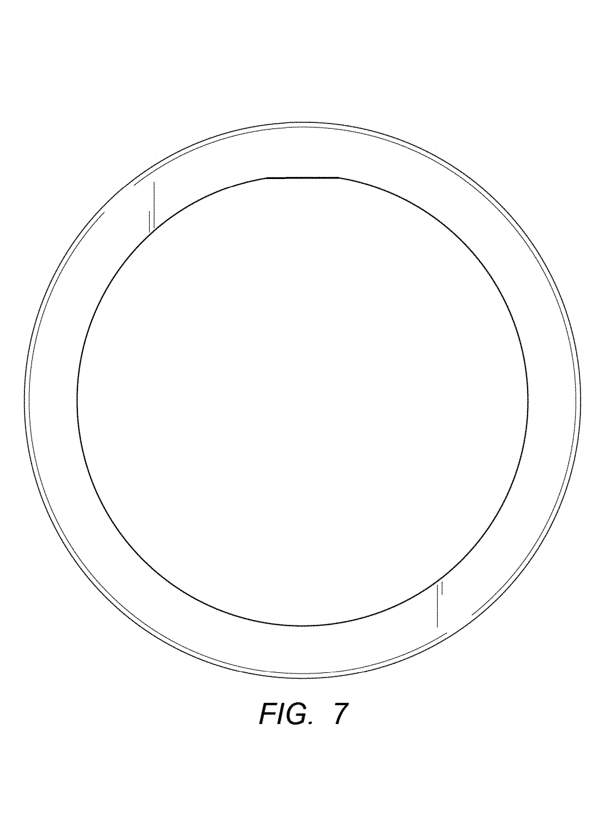
FIG. 7 is a top plan view thereof;
FIG. 8 is a bottom plan view thereof;
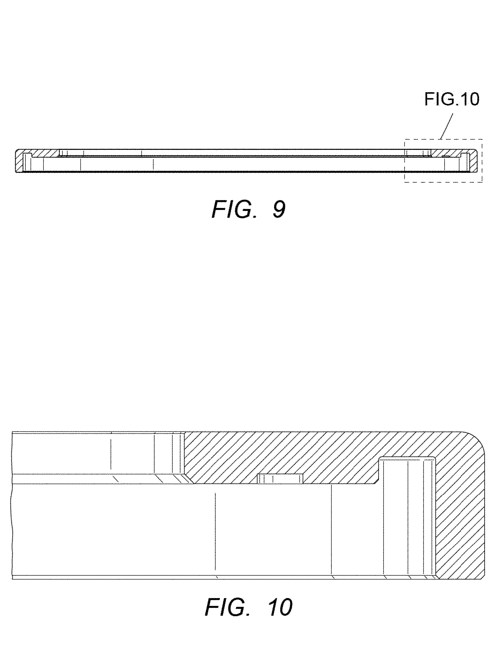
FIG. 9 is a cross-sectional view taken along line 9-9 of FIG. 3; and,
FIG. 10 is an enlarged view of the portion shown in BOX 10 in FIG. 9.
The box labeled FIG. 10 in FIG. 9 is shown in broken lines and forms no part of the claimed design.
* * * * *
D00000
D00001
D00002
D00003
D00004
D00005
XML
uspto.report is an independent third-party trademark research tool that is not affiliated, endorsed, or sponsored by the United States Patent and Trademark Office (USPTO) or any other governmental organization. The information provided by uspto.report is based on publicly available data at the time of writing and is intended for informational purposes only.
While we strive to provide accurate and up-to-date information, we do not guarantee the accuracy, completeness, reliability, or suitability of the information displayed on this site. The use of this site is at your own risk. Any reliance you place on such information is therefore strictly at your own risk.
All official trademark data, including owner information, should be verified by visiting the official USPTO website at www.uspto.gov. This site is not intended to replace professional legal advice and should not be used as a substitute for consulting with a legal professional who is knowledgeable about trademark law.