Substrate-less stackable package with wire-bond interconnect
Mohammed Dec
U.S. patent number 10,510,659 [Application Number 16/202,392] was granted by the patent office on 2019-12-17 for substrate-less stackable package with wire-bond interconnect. This patent grant is currently assigned to Invensas Corporation. The grantee listed for this patent is Invensas Corporation. Invention is credited to Ilyas Mohammed.


View All Diagrams
| United States Patent | 10,510,659 |
| Mohammed | December 17, 2019 |
Substrate-less stackable package with wire-bond interconnect
Abstract
A method for making a microelectronic unit includes forming a plurality of wire bonds on a first surface in the form of a conductive bonding surface of a structure comprising a patternable metallic element. The wire bonds are formed having bases joined to the first surface and end surfaces remote from the first surface. The wire bonds have edge surfaces extending between the bases and the end surfaces. The method also includes forming a dielectric encapsulation layer over a portion of the first surface of the conductive layer and over portions of the wire bonds such that unencapsulated portions of the wire bonds are defined by end surfaces or portions of the edge surfaces that are uncovered by the encapsulation layer. The metallic element is patterned to form first conductive elements beneath the wire bonds and insulated from one another by portions of the encapsulation layer.
| Inventors: | Mohammed; Ilyas (Santa Clara, CA) | ||||||||||
|---|---|---|---|---|---|---|---|---|---|---|---|
| Applicant: |
|
||||||||||
| Assignee: | Invensas Corporation (San Jose,
CA) |
||||||||||
| Family ID: | 48483250 | ||||||||||
| Appl. No.: | 16/202,392 | ||||||||||
| Filed: | November 28, 2018 |
Prior Publication Data
| Document Identifier | Publication Date | |
|---|---|---|
| US 20190096803 A1 | Mar 28, 2019 | |
Related U.S. Patent Documents
| Application Number | Filing Date | Patent Number | Issue Date | ||
|---|---|---|---|---|---|
| 15951925 | Apr 12, 2018 | 10170412 | |||
| 15042034 | Apr 24, 2018 | 9953914 | |||
| 14486867 | Feb 16, 2016 | 9263413 | |||
| 13477532 | Sep 16, 2014 | 8835228 | |||
| Current U.S. Class: | 1/1 |
| Current CPC Class: | H01L 24/18 (20130101); H01L 21/76892 (20130101); H01L 24/06 (20130101); H01L 21/563 (20130101); H01L 24/49 (20130101); H01L 23/5389 (20130101); H01L 21/76877 (20130101); H01L 23/5226 (20130101); H01L 25/105 (20130101); H01L 24/20 (20130101); H05K 3/4046 (20130101); H01L 24/19 (20130101); H01L 24/96 (20130101); H01L 25/0657 (20130101); H01L 2225/1052 (20130101); H01L 2224/45124 (20130101); H01L 21/568 (20130101); H01L 2224/04105 (20130101); H01L 2224/45664 (20130101); H01L 2224/49 (20130101); H01L 2924/18162 (20130101); H01L 2224/45144 (20130101); H01L 2224/45565 (20130101); H01L 2924/00011 (20130101); H05K 2203/1461 (20130101); H01L 2225/06548 (20130101); H01L 2924/00014 (20130101); H01L 24/46 (20130101); H01L 2225/1035 (20130101); H01L 2224/32245 (20130101); H01L 2924/12042 (20130101); H01L 2924/181 (20130101); H05K 2201/10287 (20130101); H01L 2224/4569 (20130101); H01L 2224/45139 (20130101); H01L 2224/45624 (20130101); H01L 2924/15311 (20130101); H01L 2224/73267 (20130101); H01L 2224/04042 (20130101); H01L 2924/01049 (20130101); H01L 24/45 (20130101); H01L 2224/45147 (20130101); H01L 2924/00012 (20130101); H01L 2924/191 (20130101); H01L 2924/19107 (20130101); H01L 2224/45655 (20130101); H01L 2225/1058 (20130101); H01L 2225/06558 (20130101); H01L 2224/45155 (20130101); H01L 2225/06524 (20130101); H01L 2224/32145 (20130101); H01L 2224/45669 (20130101); H01L 2924/182 (20130101); H01L 2224/45101 (20130101); H01L 2224/48 (20130101); H01L 2924/00014 (20130101); H01L 2224/48 (20130101); H01L 2224/45144 (20130101); H01L 2924/00014 (20130101); H01L 2224/45124 (20130101); H01L 2924/00014 (20130101); H01L 2224/45147 (20130101); H01L 2924/00014 (20130101); H01L 2224/45139 (20130101); H01L 2924/00 (20130101); H01L 2924/12042 (20130101); H01L 2924/00 (20130101); H01L 2924/181 (20130101); H01L 2924/00012 (20130101); H01L 2224/45565 (20130101); H01L 2224/45147 (20130101); H01L 2224/45664 (20130101); H01L 2224/45565 (20130101); H01L 2224/45124 (20130101); H01L 2224/45664 (20130101); H01L 2224/45664 (20130101); H01L 2924/00014 (20130101); H01L 2224/45624 (20130101); H01L 2924/00014 (20130101); H01L 2224/45655 (20130101); H01L 2924/00014 (20130101); H01L 2224/45669 (20130101); H01L 2924/00014 (20130101); H01L 2224/4569 (20130101); H01L 2924/00014 (20130101); H01L 2224/45155 (20130101); H01L 2924/00014 (20130101); H01L 2224/45101 (20130101); H01L 2924/014 (20130101); H01L 2924/00014 (20130101); H01L 2924/00011 (20130101); H01L 2924/01049 (20130101) |
| Current International Class: | H01L 23/522 (20060101); H05K 3/40 (20060101); H01L 23/538 (20060101); H01L 23/00 (20060101); H01L 25/065 (20060101); H01L 25/10 (20060101); H01L 21/56 (20060101); H01L 21/768 (20060101) |
References Cited [Referenced By]
U.S. Patent Documents
| 2230663 | February 1941 | Alden |
| 3289452 | December 1966 | Koellner |
| 3358897 | December 1967 | Christensen |
| 3430835 | March 1969 | Grable et al. |
| 3623649 | November 1971 | Keisling |
| 3795037 | March 1974 | Luttmer |
| 3900153 | August 1975 | Beerwerth et al. |
| 4067104 | January 1978 | Tracy |
| 4072816 | February 1978 | Gedney et al. |
| 4213556 | July 1980 | Persson et al. |
| 4327860 | May 1982 | Kirshenboin et al. |
| 4422568 | December 1983 | Elles et al. |
| 4437604 | March 1984 | Razon et al. |
| 4604644 | August 1986 | Beckham et al. |
| 4642889 | February 1987 | Grabbe |
| 4667267 | May 1987 | Hernandez et al. |
| 4695870 | September 1987 | Patraw |
| 4716049 | December 1987 | Patraw |
| 4725692 | February 1988 | Ishii et al. |
| 4771930 | September 1988 | Gillotti et al. |
| 4793814 | December 1988 | Zifcak et al. |
| 4804132 | February 1989 | DiFrancesco |
| 4845354 | July 1989 | Gupta et al. |
| 4867267 | September 1989 | Carlson |
| 4902600 | February 1990 | Tamagawa et al. |
| 4924353 | May 1990 | Patraw |
| 4925083 | May 1990 | Farassat et al. |
| 4955523 | September 1990 | Carlommagno et al. |
| 4975079 | December 1990 | Beaman et al. |
| 4982265 | January 1991 | Watanabe et al. |
| 4998885 | March 1991 | Beaman et al. |
| 4999472 | March 1991 | Neinast et al. |
| 5067007 | November 1991 | Otsuka et al. |
| 5067382 | November 1991 | Zimmerman et al. |
| 5083697 | January 1992 | DiFrancesco |
| 5095187 | March 1992 | Gliga |
| 5133495 | July 1992 | Angulas et al. |
| 5138438 | August 1992 | Masayuki et al. |
| 5148265 | September 1992 | Khandros et al. |
| 5148266 | September 1992 | Khandros et al. |
| 5186381 | February 1993 | Kim |
| 5189505 | February 1993 | Bartelink |
| 5196726 | March 1993 | Nishiguchi et al. |
| 5203075 | April 1993 | Angulas et al. |
| 5214308 | May 1993 | Nishiguchi et al. |
| 5220489 | June 1993 | Barreto et al. |
| 5222014 | June 1993 | Lin |
| 5238173 | August 1993 | Ura et al. |
| 5241454 | August 1993 | Ameen et al. |
| 5241456 | August 1993 | Marcinkiewicz et al. |
| 5316788 | May 1994 | Dibble et al. |
| 5340771 | August 1994 | Rostoker |
| 5346118 | September 1994 | Degani et al. |
| 5371654 | December 1994 | Beaman et al. |
| 5397997 | March 1995 | Tuckerman et al. |
| 5438224 | August 1995 | Papageorge et al. |
| 5455390 | October 1995 | DiStefano et al. |
| 5468995 | November 1995 | Higgins, III |
| 5476211 | December 1995 | Khandros |
| 5494667 | February 1996 | Uchida et al. |
| 5495667 | March 1996 | Farnworth et al. |
| 5518964 | May 1996 | DiStefano et al. |
| 5531022 | July 1996 | Beaman et al. |
| 5536909 | July 1996 | DiStefano et al. |
| 5541567 | July 1996 | Fogel et al. |
| 5571428 | November 1996 | Nishimura et al. |
| 5578869 | November 1996 | Hoffman et al. |
| 5608265 | March 1997 | Kitano et al. |
| 5615824 | April 1997 | Fjelstad et al. |
| 5616952 | April 1997 | Nakano et al. |
| 5635846 | June 1997 | Beaman et al. |
| 5656550 | August 1997 | Tsuji et al. |
| 5659952 | August 1997 | Kovac et al. |
| 5679977 | October 1997 | Khandros et al. |
| 5688716 | November 1997 | DiStefano et al. |
| 5718361 | February 1998 | Braun et al. |
| 5726493 | March 1998 | Yamashita et al. |
| 5731709 | March 1998 | Pastore et al. |
| 5736780 | April 1998 | Murayama |
| 5736785 | April 1998 | Chiang et al. |
| 5766987 | June 1998 | Mitchell et al. |
| 5787581 | August 1998 | DiStefano et al. |
| 5801441 | September 1998 | DiStefano et al. |
| 5802699 | September 1998 | Fjelstad et al. |
| 5811982 | September 1998 | Beaman et al. |
| 5821763 | October 1998 | Beaman et al. |
| 5830389 | November 1998 | Capote et al. |
| 5831836 | November 1998 | Long et al. |
| 5839191 | November 1998 | Economy et al. |
| 5854507 | December 1998 | Miremadi et al. |
| 5874781 | February 1999 | Fogal et al. |
| 5898991 | May 1999 | Fogel et al. |
| 5908317 | June 1999 | Heo |
| 5912505 | June 1999 | Itoh et al. |
| 5948533 | September 1999 | Gallagher et al. |
| 5953624 | September 1999 | Bando et al. |
| 5971253 | October 1999 | Gilleo et al. |
| 5973391 | October 1999 | Bischoff et al. |
| 5977618 | November 1999 | DiStefano et al. |
| 5977640 | November 1999 | Bertin et al. |
| 5980270 | November 1999 | Fjelstad et al. |
| 5989936 | November 1999 | Smith et al. |
| 5994152 | November 1999 | Khandros et al. |
| 6000126 | December 1999 | Pai |
| 6002168 | December 1999 | Bellaar et al. |
| 6032359 | March 2000 | Carroll |
| 6038136 | March 2000 | Weber |
| 6052287 | April 2000 | Palmer et al. |
| 6054337 | April 2000 | Solberg |
| 6054756 | April 2000 | DiStefano et al. |
| 6077380 | June 2000 | Hayes et al. |
| 6117694 | September 2000 | Smith et al. |
| 6121676 | September 2000 | Solberg |
| 6124546 | September 2000 | Hayward et al. |
| 6133072 | October 2000 | Fjelstad |
| 6145733 | November 2000 | Streckfuss et al. |
| 6157080 | December 2000 | Tamaki et al. |
| 6158647 | December 2000 | Chapman et al. |
| 6164523 | December 2000 | Fauty et al. |
| 6168965 | January 2001 | Malinovich et al. |
| 6177636 | January 2001 | Fjelstad |
| 6180881 | January 2001 | Isaak |
| 6194250 | February 2001 | Melton et al. |
| 6194291 | February 2001 | DiStefano et al. |
| 6202297 | March 2001 | Faraci et al. |
| 6206273 | March 2001 | Beaman et al. |
| 6208024 | March 2001 | DiStefano |
| 6211572 | April 2001 | Fjelstad et al. |
| 6211574 | April 2001 | Tao et al. |
| 6215670 | April 2001 | Khandros |
| 6218728 | April 2001 | Kimura |
| 6225688 | May 2001 | Kim et al. |
| 6238949 | May 2001 | Nguyen et al. |
| 6258625 | July 2001 | Brofman et al. |
| 6260264 | July 2001 | Chen et al. |
| 6262482 | July 2001 | Shiraishi et al. |
| 6268662 | July 2001 | Test et al. |
| 6295729 | October 2001 | Beaman et al. |
| 6300780 | October 2001 | Beaman et al. |
| 6303997 | October 2001 | Lee et al. |
| 6313528 | November 2001 | Solberg |
| 6316838 | November 2001 | Ozawa et al. |
| 6329224 | December 2001 | Nguyen et al. |
| 6332270 | December 2001 | Beaman et al. |
| 6334247 | January 2002 | Beaman et al. |
| 6358627 | March 2002 | Benenati et al. |
| 6362520 | March 2002 | DiStefano |
| 6362525 | March 2002 | Rahim |
| 6376769 | April 2002 | Chung |
| 6388333 | May 2002 | Taniguchi et al. |
| 6395199 | May 2002 | Krassowski et al. |
| 6399426 | June 2002 | Capote et al. |
| 6407448 | June 2002 | Chun |
| 6407456 | June 2002 | Ball |
| 6410431 | June 2002 | Bertin et al. |
| 6413850 | July 2002 | Ooroku et al. |
| 6439450 | August 2002 | Chapman et al. |
| 6458411 | October 2002 | Goossen et al. |
| 6469260 | October 2002 | Horiuchi et al. |
| 6469373 | October 2002 | Funakura et al. |
| 6472743 | October 2002 | Huang et al. |
| 6476503 | November 2002 | Imamura et al. |
| 6476506 | November 2002 | O'Connor |
| 6476583 | November 2002 | McAndrews |
| 6486545 | November 2002 | Glenn et al. |
| 6489182 | December 2002 | Kwon |
| 6489676 | December 2002 | Taniguchi et al. |
| 6495914 | December 2002 | Sekine et al. |
| 6507104 | January 2003 | Ho et al. |
| 6509639 | January 2003 | Lin |
| 6514847 | February 2003 | Ohsawa et al. |
| 6515355 | February 2003 | Jiang et al. |
| 6522018 | February 2003 | Tay et al. |
| 6550666 | February 2003 | Chew et al. |
| 6526655 | March 2003 | Beaman et al. |
| 6531784 | March 2003 | Shim et al. |
| 6538336 | March 2003 | Secker et al. |
| 6545228 | April 2003 | Hashimoto |
| 6555918 | April 2003 | Masuda et al. |
| 6560117 | May 2003 | Moon |
| 6563205 | May 2003 | Fogal et al. |
| 6563217 | May 2003 | Corisis et al. |
| 6573458 | June 2003 | Matsubara et al. |
| 6578754 | June 2003 | Tung |
| 6581276 | June 2003 | Chung |
| 6581283 | June 2003 | Sugiura et al. |
| 6624653 | September 2003 | Cram |
| 6630730 | October 2003 | Grigg |
| 6639303 | October 2003 | Siniaguine |
| 6647310 | November 2003 | Yi et al. |
| 6650013 | November 2003 | Yin et al. |
| 6653170 | November 2003 | Lin |
| 6684007 | January 2004 | Yoshimura et al. |
| 6686268 | February 2004 | Farnworth et al. |
| 6687988 | February 2004 | Sugiura et al. |
| 6693363 | February 2004 | Tay et al. |
| 6696305 | February 2004 | Kung et al. |
| 6699730 | March 2004 | Kim et al. |
| 6708403 | March 2004 | Beaman et al. |
| 6720783 | April 2004 | Satoh et al. |
| 6730544 | May 2004 | Yang |
| 6733711 | May 2004 | Durocher et al. |
| 6734539 | May 2004 | Degani et al. |
| 6734542 | May 2004 | Nakatani et al. |
| 6740980 | May 2004 | Hirose |
| 6740981 | May 2004 | Hosomi |
| 6741085 | May 2004 | Khandros et al. |
| 6746894 | June 2004 | Fee et al. |
| 6754407 | June 2004 | Chakravorty et al. |
| 6756252 | June 2004 | Nakanishi |
| 6756663 | June 2004 | Shiraishi et al. |
| 6759738 | July 2004 | Fallon et al. |
| 6762078 | July 2004 | Shin et al. |
| 6765287 | July 2004 | Lin |
| 6774317 | August 2004 | Fjelstad |
| 6774467 | August 2004 | Horiuchi et al. |
| 6774473 | August 2004 | Shen |
| 6774494 | August 2004 | Arakawa |
| 6777787 | August 2004 | Shibata |
| 6777797 | August 2004 | Egawa |
| 6778406 | August 2004 | Eldridge et al. |
| 6780746 | August 2004 | Kinsman et al. |
| 6787926 | September 2004 | Chen et al. |
| 6790757 | September 2004 | Chittipeddi et al. |
| 6800941 | October 2004 | Lee et al. |
| 6812575 | November 2004 | Furusawa |
| 6815257 | November 2004 | Yoon et al. |
| 6825552 | November 2004 | Light et al. |
| 6828665 | December 2004 | Pu et al. |
| 6828668 | December 2004 | Smith et al. |
| 6844619 | January 2005 | Tago |
| 6856235 | February 2005 | Fjelstad |
| 6864166 | March 2005 | Yin et al. |
| 6867499 | March 2005 | Tabirzi |
| 6874910 | April 2005 | Sugimoto et al. |
| 6897565 | May 2005 | Pflughaupt et al. |
| 6900530 | May 2005 | Tsai |
| 6902869 | June 2005 | Appelt et al. |
| 6902950 | June 2005 | Ma et al. |
| 6906408 | June 2005 | Cloud et al. |
| 6908785 | June 2005 | Kim |
| 6909181 | June 2005 | Aiba et al. |
| 6917098 | July 2005 | Yamunan |
| 6930256 | August 2005 | Kluemoeller et al. |
| 6933598 | August 2005 | Kamezos |
| 6933608 | August 2005 | Fujisawa |
| 6939723 | September 2005 | Corisis et al. |
| 6946380 | September 2005 | Takahashi |
| 6951773 | October 2005 | Ho et al. |
| 6962282 | November 2005 | Manansala |
| 6962864 | November 2005 | Jeng et al. |
| 6977440 | December 2005 | Pflughaupt et al. |
| 6979599 | December 2005 | Silverbrook |
| 6987032 | January 2006 | Fan et al. |
| 6989122 | January 2006 | Pham et al. |
| 7009297 | March 2006 | Chiang et al. |
| 7017794 | March 2006 | Nosaka |
| 7021521 | April 2006 | Sakurai et al. |
| 7045884 | May 2006 | Standing |
| 7051915 | May 2006 | Mutaguchi |
| 7052935 | May 2006 | Pai et al. |
| 7053477 | May 2006 | Kamezos et al. |
| 7053485 | May 2006 | Bang et al. |
| 7061079 | June 2006 | Weng et al. |
| 7061097 | June 2006 | Yokoi |
| 7067911 | June 2006 | Lin et al. |
| 7071028 | July 2006 | Koike et al. |
| 7071547 | July 2006 | Kang et al. |
| 7071573 | July 2006 | Lin |
| 7078788 | July 2006 | Vu et al. |
| 7078822 | July 2006 | Dias et al. |
| 7095105 | August 2006 | Cherukuri et al. |
| 7112520 | September 2006 | Lee et al. |
| 7115986 | October 2006 | Moon et al. |
| 7119427 | October 2006 | Kim |
| 7121891 | October 2006 | Cherian |
| 7138722 | November 2006 | Miyamoto et al. |
| 7170185 | January 2007 | Hogerton et al. |
| 7176043 | February 2007 | Haba et al. |
| 7176506 | February 2007 | Beroz et al. |
| 7176559 | February 2007 | Ho et al. |
| 7185426 | March 2007 | Hiner et al. |
| 7187072 | March 2007 | Fukitomi et al. |
| 7190061 | March 2007 | Lee |
| 7198980 | April 2007 | Jiang et al. |
| 7198987 | April 2007 | Warren et al. |
| 7205670 | April 2007 | Oyama |
| 7215033 | May 2007 | Lee et al. |
| 7216794 | May 2007 | Lange et al. |
| 7225538 | June 2007 | Eldridge et al. |
| 7227095 | June 2007 | Roberts et al. |
| 7229906 | June 2007 | Baninetz et al. |
| 7233057 | June 2007 | Hussa |
| 7242081 | July 2007 | Lee |
| 7246431 | July 2007 | Bang et al. |
| 7256069 | August 2007 | Akram et al. |
| 7259445 | August 2007 | Lau et al. |
| 7262124 | August 2007 | Fujisawa |
| 7262506 | August 2007 | Mess et al. |
| 7268421 | September 2007 | Lin |
| 7276785 | October 2007 | Bauer et al. |
| 7276799 | October 2007 | Lee et al. |
| 7287322 | October 2007 | Mahieu et al. |
| 7290448 | November 2007 | Shirasaka et al. |
| 7294920 | November 2007 | Chen et al. |
| 7294928 | November 2007 | Bang et al. |
| 7298033 | November 2007 | Yoo |
| 7301770 | November 2007 | Campbell et al. |
| 7307348 | December 2007 | Wood et al. |
| 7321164 | January 2008 | Hsu |
| 7323767 | January 2008 | James et al. |
| 7327038 | February 2008 | Kwon et al. |
| 7342803 | March 2008 | Inagaki et al. |
| 7344917 | March 2008 | Gautham |
| 7345361 | March 2008 | Malik et al. |
| 7355289 | April 2008 | Hess et al. |
| 7365416 | April 2008 | Kawabata et al. |
| 7368924 | May 2008 | Beaman et al. |
| 7371676 | May 2008 | Hembree |
| 7372151 | May 2008 | Fan et al. |
| 7378726 | May 2008 | Punzalan et al. |
| 7390700 | June 2008 | Gerber et al. |
| 7391105 | June 2008 | Yeom |
| 7391121 | June 2008 | Otremba |
| 7416107 | August 2008 | Chapman et al. |
| 7425758 | September 2008 | Corisis et al. |
| 7453157 | November 2008 | Haba et al. |
| 7456091 | November 2008 | Kuraya et al. |
| 7456495 | November 2008 | Pohl et al. |
| 7459348 | December 2008 | Saeki |
| 7462936 | December 2008 | Haba et al. |
| 7476608 | January 2009 | Craig et al. |
| 7476962 | January 2009 | Kim |
| 7485562 | February 2009 | Chua et al. |
| 7485969 | February 2009 | Corisis et al. |
| 7495179 | February 2009 | Kubota et al. |
| 7495342 | February 2009 | Beaman et al. |
| 7495644 | February 2009 | Hirakata |
| 7504284 | March 2009 | Ye et al. |
| 7504716 | March 2009 | Abbott |
| 7517733 | April 2009 | Camacho et al. |
| 7527505 | May 2009 | Murata |
| 7528474 | May 2009 | Lee |
| 7535090 | May 2009 | Furuyama et al. |
| 7537962 | May 2009 | Jang et al. |
| 7538565 | May 2009 | Beaman et al. |
| 7547624 | June 2009 | Tanaka |
| 7550836 | June 2009 | Chou et al. |
| 7560360 | July 2009 | Cheng et al. |
| 7564116 | July 2009 | Ahn et al. |
| 7576415 | August 2009 | Cha et al. |
| 7576439 | August 2009 | Craig et al. |
| 7578422 | August 2009 | Lange et al. |
| 7582963 | September 2009 | Gerber et al. |
| 7589394 | September 2009 | Kawano |
| 7592638 | September 2009 | Kim |
| 7595548 | September 2009 | Shirasaka et al. |
| 7605479 | October 2009 | Mohammed |
| 7612638 | November 2009 | Chung et al. |
| 7621436 | November 2009 | Mii et al. |
| 7625781 | December 2009 | Beer |
| 7629695 | December 2009 | Yoshimura et al. |
| 7633154 | December 2009 | Dai et al. |
| 7633765 | December 2009 | Scanlan et al. |
| 7642133 | January 2010 | Wu et al. |
| 7646102 | January 2010 | Boon |
| 7659612 | February 2010 | Hembree et al. |
| 7659617 | February 2010 | Kang et al. |
| 7663226 | February 2010 | Cho et al. |
| 7670940 | March 2010 | Mizukoshi et al. |
| 7671457 | March 2010 | Hiner et al. |
| 7671459 | March 2010 | Corisis et al. |
| 7675152 | March 2010 | Gerber et al. |
| 7677429 | March 2010 | Chapman et al. |
| 7682960 | March 2010 | Wen |
| 7682962 | March 2010 | Hembree |
| 7683460 | March 2010 | Heitzer et al. |
| 7683482 | March 2010 | Nishida et al. |
| 7692931 | April 2010 | Chong et al. |
| 7696631 | April 2010 | Beaulieu et al. |
| 7706144 | April 2010 | Lynch |
| 7709968 | May 2010 | Damberg et al. |
| 7719122 | May 2010 | Tsao et al. |
| 7723839 | May 2010 | Yano et al. |
| 7728443 | June 2010 | Hembree |
| 7737545 | June 2010 | Fjelstad et al. |
| 7750483 | July 2010 | Lin et al. |
| 7757385 | July 2010 | Hembree |
| 7759782 | July 2010 | Haba et al. |
| 7777238 | August 2010 | Nishida et al. |
| 7777328 | August 2010 | Enomoto |
| 7777351 | August 2010 | Berry et al. |
| 7780064 | August 2010 | Wong et al. |
| 7781877 | August 2010 | Jiang et al. |
| 7795717 | September 2010 | Goller |
| 7800233 | September 2010 | Kawano et al. |
| 7807512 | October 2010 | Lee et al. |
| 7808093 | October 2010 | Kagaya et al. |
| 7808439 | October 2010 | Yang et al. |
| 7815323 | October 2010 | Saeki |
| 7834464 | November 2010 | Meyer et al. |
| 7838334 | November 2010 | Yu et al. |
| 7842541 | November 2010 | Rusli et al. |
| 7850087 | December 2010 | Hwang et al. |
| 7851259 | December 2010 | Kim |
| 7855462 | December 2010 | Boon et al. |
| 7855464 | December 2010 | Shikano |
| 7857190 | December 2010 | Takahashi et al. |
| 7859033 | December 2010 | Brady |
| 7872335 | January 2011 | Khan et al. |
| 7876180 | January 2011 | Uchimura |
| 7880290 | February 2011 | Park |
| 7892889 | February 2011 | Howard et al. |
| 7898083 | March 2011 | Castro |
| 7901989 | March 2011 | Haba et al. |
| 7902644 | March 2011 | Huang et al. |
| 7902652 | March 2011 | Seo et al. |
| 7910385 | March 2011 | Kweon et al. |
| 7911805 | March 2011 | Haba |
| 7919846 | April 2011 | Hembree |
| 7919871 | April 2011 | Moon et al. |
| 7923295 | April 2011 | Shim et al. |
| 7923304 | April 2011 | Choi et al. |
| 7928552 | April 2011 | Cho et al. |
| 7932170 | April 2011 | Huemoeller et al. |
| 7934313 | May 2011 | Lin et al. |
| 7939934 | May 2011 | Haba et al. |
| 7943436 | May 2011 | McElvain |
| 7944034 | May 2011 | Gerber et al. |
| 7956456 | June 2011 | Gurrum et al. |
| 7960843 | June 2011 | Hedler et al. |
| 7964956 | June 2011 | Bet-Shliemoun |
| 7967062 | June 2011 | Campbell et al. |
| 7974099 | July 2011 | Grajcar |
| 7977597 | July 2011 | Robert et al. |
| 7990711 | August 2011 | Andry et al. |
| 7994622 | August 2011 | Mohammed et al. |
| 8004074 | August 2011 | Mori et al. |
| 8004093 | August 2011 | Oh et al. |
| 8008121 | August 2011 | Choi et al. |
| 8012797 | September 2011 | Shen et al. |
| 8017437 | September 2011 | Yoo et al. |
| 8017452 | September 2011 | Ishihara et al. |
| 8018033 | September 2011 | Moriya |
| 8018065 | September 2011 | Lam |
| 8020290 | September 2011 | Sheats |
| 8021907 | September 2011 | Pagaila et al. |
| 8035213 | October 2011 | Lee et al. |
| 8039316 | October 2011 | Chi et al. |
| 8039960 | October 2011 | Lin |
| 8039970 | October 2011 | Yamamori et al. |
| 8048479 | November 2011 | Hedler et al. |
| 8053814 | November 2011 | Chen et al. |
| 8053879 | November 2011 | Lee et al. |
| 8053906 | November 2011 | Chang et al. |
| 8058101 | November 2011 | Haba et al. |
| 8063475 | November 2011 | Choi et al. |
| 8071424 | December 2011 | Kang et al. |
| 8071431 | December 2011 | Hoang et al. |
| 8071470 | December 2011 | Khor et al. |
| 8076765 | December 2011 | Chen et al. |
| 8076770 | December 2011 | Kagaya et al. |
| 8080445 | December 2011 | Pagaila |
| 8084867 | December 2011 | Tang et al. |
| 8092734 | January 2012 | Jiang et al. |
| 8093697 | January 2012 | Haba et al. |
| 8106498 | January 2012 | Shin et al. |
| 8115283 | February 2012 | Bolognia et al. |
| 8119516 | February 2012 | Endo |
| 8120054 | February 2012 | Seo et al. |
| 8120186 | February 2012 | Yoon |
| 8138584 | March 2012 | Wang et al. |
| 8143141 | March 2012 | Sun et al. |
| 8143710 | March 2012 | Cho |
| 8158888 | April 2012 | Shen et al. |
| 8169065 | May 2012 | Kohl et al. |
| 8174119 | May 2012 | Pendse |
| 8183682 | May 2012 | Groenhuis et al. |
| 8183684 | May 2012 | Nakazato |
| 8193034 | June 2012 | Pagaila et al. |
| 8194411 | June 2012 | Leung et al. |
| 8198716 | June 2012 | Periaman et al. |
| 8207604 | June 2012 | Haba et al. |
| 8213184 | July 2012 | Knickerbocker |
| 8217502 | July 2012 | Ko |
| 8225982 | July 2012 | Pirkle et al. |
| 8232141 | July 2012 | Choi et al. |
| 8237257 | August 2012 | Yang |
| 8258010 | September 2012 | Pagaila et al. |
| 8258015 | September 2012 | Chow et al. |
| 8263435 | September 2012 | Choi et al. |
| 8264091 | September 2012 | Cho et al. |
| 8269335 | September 2012 | Osumi |
| 8278746 | October 2012 | Ding et al. |
| 8288854 | October 2012 | Weng et al. |
| 8293580 | October 2012 | Kim et al. |
| 8299368 | October 2012 | Endo |
| 8304900 | November 2012 | Jang et al. |
| 8314492 | November 2012 | Egawa |
| 8315060 | November 2012 | Morikita et al. |
| 8318539 | November 2012 | Cho et al. |
| 8319338 | November 2012 | Berry et al. |
| 8324633 | December 2012 | McKenzie et al. |
| 8330272 | December 2012 | Haba |
| 8349735 | January 2013 | Pagaila et al. |
| 8354297 | January 2013 | Pagaila et al. |
| 8362620 | January 2013 | Pagani |
| 8372741 | February 2013 | Co et al. |
| 8390108 | March 2013 | Cho et al. |
| 8390117 | March 2013 | Shimizu et al. |
| 8395259 | March 2013 | Eun |
| 8399972 | March 2013 | Hoang et al. |
| 8404520 | March 2013 | Chau et al. |
| 8409922 | April 2013 | Camacho et al. |
| 8415704 | April 2013 | Ivanov et al. |
| 8419442 | April 2013 | Horikawa et al. |
| 8420430 | April 2013 | Chiu et al. |
| 8435899 | May 2013 | Miyata et al. |
| 8450839 | May 2013 | Corisis et al. |
| 8476115 | July 2013 | Choi et al. |
| 8476770 | July 2013 | Shao et al. |
| 8482111 | July 2013 | Haba |
| 8487421 | July 2013 | Sato et al. |
| 8492201 | July 2013 | Pagaila et al. |
| 8502387 | August 2013 | Choi et al. |
| 8507297 | August 2013 | Iida et al. |
| 8508045 | August 2013 | Khan et al. |
| 8518746 | August 2013 | Pagaila et al. |
| 8520396 | August 2013 | Schmidt et al. |
| 8525214 | September 2013 | Lin et al. |
| 8525314 | September 2013 | Haba et al. |
| 8525318 | September 2013 | Kim et al. |
| 8552556 | October 2013 | Kim et al. |
| 8558379 | October 2013 | Kwon |
| 8558392 | October 2013 | Chua et al. |
| 8564141 | October 2013 | Lee et al. |
| 8567051 | October 2013 | Val |
| 8569892 | October 2013 | Mori et al. |
| 8580607 | November 2013 | Haba |
| 8598717 | December 2013 | Masuda |
| 8618646 | December 2013 | Sasaki et al. |
| 8618659 | December 2013 | Sato et al. |
| 8624374 | January 2014 | Ding et al. |
| 8633059 | January 2014 | Do et al. |
| 8637991 | January 2014 | Haba |
| 8642393 | February 2014 | Yu et al. |
| 8646508 | February 2014 | Kawada |
| 8653626 | February 2014 | Lo et al. |
| 8653668 | February 2014 | Uno et al. |
| 8653676 | February 2014 | Kim et al. |
| 8659164 | February 2014 | Haba |
| 8664780 | March 2014 | Han et al. |
| 8669646 | March 2014 | Tabatabai et al. |
| 8670261 | March 2014 | Crisp et al. |
| 8680662 | March 2014 | Haba et al. |
| 8680677 | March 2014 | Wyland |
| 8680684 | March 2014 | Haba et al. |
| 8685792 | April 2014 | Chow et al. |
| 8686570 | April 2014 | Semmelmeyer et al. |
| 8697492 | April 2014 | Haba et al. |
| 8723307 | May 2014 | Jiang et al. |
| 8728865 | May 2014 | Haba et al. |
| 8729714 | May 2014 | Meyer |
| 8742576 | June 2014 | Thacker et al. |
| 8742597 | June 2014 | Nickerson |
| 8766436 | July 2014 | Delucca et al. |
| 8772152 | July 2014 | Co et al. |
| 8772817 | July 2014 | Yao |
| 8785245 | July 2014 | Kim |
| 8791575 | July 2014 | Oganesian et al. |
| 8791580 | July 2014 | Park et al. |
| 8796135 | August 2014 | Oganesian et al. |
| 8796846 | August 2014 | Lin et al. |
| 8802494 | August 2014 | Lee et al. |
| 8810031 | August 2014 | Chang et al. |
| 8811055 | August 2014 | Yoon |
| 8816404 | August 2014 | Kim et al. |
| 8816505 | August 2014 | Mohammed et al. |
| 8835228 | September 2014 | Mohammed |
| 8836136 | September 2014 | Chau et al. |
| 8836140 | September 2014 | Ma et al. |
| 8836147 | September 2014 | Uno et al. |
| 8841765 | September 2014 | Haba et al. |
| 8846521 | September 2014 | Sugizaki |
| 8847376 | September 2014 | Oganesian et al. |
| 8853558 | October 2014 | Gupta et al. |
| 8878353 | November 2014 | Haba et al. |
| 8881086 | November 2014 | McElvain |
| 8884416 | November 2014 | Lee et al. |
| 8893380 | November 2014 | Kim et al. |
| 8907466 | December 2014 | Haba |
| 8907500 | December 2014 | Haba et al. |
| 8912651 | December 2014 | Yu et al. |
| 8916781 | December 2014 | Haba et al. |
| 8922005 | December 2014 | Hu et al. |
| 8923004 | December 2014 | Low et al. |
| 8927337 | January 2015 | Haba et al. |
| 8937309 | January 2015 | England et al. |
| 8940630 | January 2015 | Damberg et al. |
| 8940636 | January 2015 | Pagaila et al. |
| 8946757 | February 2015 | Mohammed et al. |
| 8948712 | February 2015 | Chen et al. |
| 8963339 | February 2015 | He et al. |
| 8970049 | March 2015 | Kamezos |
| 8975726 | March 2015 | Chen |
| 8978247 | March 2015 | Yang et al. |
| 8981559 | March 2015 | Hsu et al. |
| 8987132 | March 2015 | Gruber et al. |
| 8988895 | March 2015 | Mohammed et al. |
| 8993376 | March 2015 | Camacho et al. |
| 9006031 | April 2015 | Camacho et al. |
| 9012263 | April 2015 | Mathew et al. |
| 9041227 | May 2015 | Chau et al. |
| 9054095 | June 2015 | Pagaila |
| 9082763 | July 2015 | Yu et al. |
| 9093435 | July 2015 | Sato et al. |
| 9095074 | July 2015 | Haba et al. |
| 9105483 | August 2015 | Chau et al. |
| 9105552 | August 2015 | Yu et al. |
| 9117811 | August 2015 | Zohni |
| 9123664 | September 2015 | Haba |
| 9128123 | September 2015 | Liu et al. |
| 9136254 | September 2015 | Zhao et al. |
| 9142586 | September 2015 | Wang et al. |
| 9153562 | October 2015 | Haba et al. |
| 9167710 | October 2015 | Mohammed et al. |
| 9171790 | October 2015 | Yu et al. |
| 9177832 | November 2015 | Camacho |
| 9196586 | November 2015 | Chen et al. |
| 9196588 | November 2015 | Leal |
| 9209081 | December 2015 | Lim et al. |
| 9214434 | December 2015 | Kim et al. |
| 9224647 | December 2015 | Koo et al. |
| 9224717 | December 2015 | Sato et al. |
| 9258922 | February 2016 | Chen et al. |
| 9263394 | February 2016 | Uzoh et al. |
| 9263413 | February 2016 | Mohammed |
| 9299670 | March 2016 | Yap et al. |
| 9318449 | April 2016 | Hasch et al. |
| 9318452 | April 2016 | Chen et al. |
| 9324696 | April 2016 | Choi et al. |
| 9330945 | May 2016 | Song et al. |
| 9349706 | May 2016 | Co et al. |
| 9362161 | June 2016 | Chi et al. |
| 9378982 | June 2016 | Lin et al. |
| 9379074 | June 2016 | Uzoh et al. |
| 9379078 | June 2016 | Yu et al. |
| 9401338 | July 2016 | Magnus et al. |
| 9405064 | August 2016 | Herbsommer et al. |
| 9412661 | August 2016 | Lu et al. |
| 9418940 | August 2016 | Hoshino et al. |
| 9418971 | August 2016 | Chen et al. |
| 9437459 | September 2016 | Carpenter et al. |
| 9443797 | September 2016 | Marimuthu et al. |
| 9449941 | September 2016 | Tsai et al. |
| 9461025 | October 2016 | Yu et al. |
| 9484331 | November 2016 | Paek et al. |
| 9496152 | November 2016 | Cho et al. |
| 9502390 | November 2016 | Caskey et al. |
| 9508622 | November 2016 | Higgins |
| 9559088 | January 2017 | Gonzalez et al. |
| 9570382 | February 2017 | Haba |
| 9583456 | February 2017 | Uzoh et al. |
| 9601454 | March 2017 | Zhao et al. |
| 9653428 | May 2017 | Hiner |
| 9653442 | May 2017 | Yu et al. |
| 9659877 | May 2017 | Bakalski et al. |
| 9663353 | May 2017 | Ofner et al. |
| 9685365 | June 2017 | Mohammed |
| 9735084 | August 2017 | Katkar et al. |
| 9788466 | October 2017 | Chen |
| 9812402 | November 2017 | Awujoola et al. |
| 9842798 | December 2017 | Marimuthu et al. |
| 9859203 | January 2018 | Kim et al. |
| 9871599 | January 2018 | Chen et al. |
| 10079225 | September 2018 | Lin et al. |
| 10115671 | October 2018 | Shenoy et al. |
| 10115678 | October 2018 | Awujoola et al. |
| 10170412 | January 2019 | Mohammed |
| 10181457 | January 2019 | Prabhu et al. |
| 2001/0042925 | November 2001 | Yamamoto et al. |
| 2002/0014004 | February 2002 | Beaman et al. |
| 2002/0125556 | September 2002 | Oh et al. |
| 2002/0171152 | November 2002 | Miyazaki |
| 2003/0006494 | January 2003 | Lee et al. |
| 2003/0048108 | March 2003 | Beaman et al. |
| 2003/0057544 | March 2003 | Nathan et al. |
| 2003/0094666 | May 2003 | Clayton et al. |
| 2003/0162378 | August 2003 | Mikami |
| 2004/0041757 | March 2004 | Yang et al. |
| 2004/0262728 | December 2004 | Sterrett et al. |
| 2005/0017369 | January 2005 | Clayton et al. |
| 2005/0062492 | March 2005 | Beaman et al. |
| 2005/0082664 | April 2005 | Funaba et al. |
| 2005/0095835 | May 2005 | Humpston et al. |
| 2005/0161814 | July 2005 | Mizukoshi et al. |
| 2005/0173807 | August 2005 | Zhu et al. |
| 2005/0176233 | August 2005 | Joshi et al. |
| 2006/0087013 | April 2006 | Hsieh |
| 2006/0216868 | September 2006 | Yang et al. |
| 2006/0255449 | November 2006 | Lee et al. |
| 2007/0010086 | January 2007 | Hsieh |
| 2007/0080360 | April 2007 | Mirsky et al. |
| 2007/0164457 | July 2007 | Yamaguchi et al. |
| 2007/0190747 | August 2007 | Hup |
| 2007/0254406 | November 2007 | Lee |
| 2007/0271781 | November 2007 | Beaman et al. |
| 2007/0290325 | December 2007 | Wu et al. |
| 2008/0006942 | January 2008 | Park et al. |
| 2008/0017968 | January 2008 | Choi et al. |
| 2008/0023805 | January 2008 | Howard et al. |
| 2008/0042265 | February 2008 | Merilo et al. |
| 2008/0047741 | February 2008 | Beaman et al. |
| 2008/0048690 | February 2008 | Beaman et al. |
| 2008/0048691 | February 2008 | Beaman et al. |
| 2008/0048697 | February 2008 | Beaman et al. |
| 2008/0054434 | March 2008 | Kim |
| 2008/0073769 | March 2008 | Wu et al. |
| 2008/0100316 | May 2008 | Beaman et al. |
| 2008/0100317 | May 2008 | Beaman et al. |
| 2008/0100318 | May 2008 | Beaman et al. |
| 2008/0100324 | May 2008 | Beaman et al. |
| 2008/0105984 | May 2008 | Lee et al. |
| 2008/0106281 | May 2008 | Beaman et al. |
| 2008/0106282 | May 2008 | Beaman et al. |
| 2008/0106283 | May 2008 | Beaman et al. |
| 2008/0106284 | May 2008 | Beaman et al. |
| 2008/0106285 | May 2008 | Beaman et al. |
| 2008/0106291 | May 2008 | Beaman et al. |
| 2008/0106872 | May 2008 | Beaman et al. |
| 2008/0111568 | May 2008 | Beaman et al. |
| 2008/0111569 | May 2008 | Beaman et al. |
| 2008/0111570 | May 2008 | Beaman et al. |
| 2008/0112144 | May 2008 | Beaman et al. |
| 2008/0112145 | May 2008 | Beaman et al. |
| 2008/0112146 | May 2008 | Beaman et al. |
| 2008/0112147 | May 2008 | Beaman et al. |
| 2008/0112148 | May 2008 | Beaman et al. |
| 2008/0112149 | May 2008 | Beaman et al. |
| 2008/0116912 | May 2008 | Beaman et al. |
| 2008/0116913 | May 2008 | Beaman et al. |
| 2008/0116914 | May 2008 | Beaman et al. |
| 2008/0116915 | May 2008 | Beaman et al. |
| 2008/0116916 | May 2008 | Beaman et al. |
| 2008/0117611 | May 2008 | Beaman et al. |
| 2008/0117612 | May 2008 | Beaman et al. |
| 2008/0117613 | May 2008 | Beaman et al. |
| 2008/0121879 | May 2008 | Beaman et al. |
| 2008/0123310 | May 2008 | Beaman et al. |
| 2008/0123319 | June 2008 | Beaman et al. |
| 2008/0123320 | June 2008 | Beaman et al. |
| 2008/0132094 | June 2008 | Beaman et al. |
| 2008/0156518 | July 2008 | Honer et al. |
| 2008/0164595 | July 2008 | Wu et al. |
| 2008/0169548 | July 2008 | Baek |
| 2008/0217708 | September 2008 | Reisner et al. |
| 2008/0246126 | October 2008 | Bowles et al. |
| 2008/0277776 | November 2008 | Enomoto |
| 2008/0280393 | November 2008 | Lee et al. |
| 2008/0284045 | November 2008 | Gerber et al. |
| 2008/0303153 | December 2008 | Oi et al. |
| 2008/0308305 | December 2008 | Kawabe |
| 2009/0008796 | January 2009 | Eng et al. |
| 2009/0014876 | January 2009 | Youn et al. |
| 2009/0032913 | February 2009 | Haba |
| 2009/0085185 | April 2009 | Byun et al. |
| 2009/0091009 | April 2009 | Corisis et al. |
| 2009/0102063 | April 2009 | Lee et al. |
| 2009/0127686 | May 2009 | Yang et al. |
| 2009/0128176 | May 2009 | Beaman et al. |
| 2009/0140415 | June 2009 | Furuta |
| 2009/0166664 | July 2009 | Park et al. |
| 2009/0166873 | July 2009 | Yang et al. |
| 2009/0189288 | August 2009 | Chung et al. |
| 2009/0194829 | August 2009 | Chung et al. |
| 2009/0256229 | October 2009 | Ishikawa et al. |
| 2009/0315579 | December 2009 | Beaman et al. |
| 2010/0032822 | February 2010 | Liao et al. |
| 2010/0044860 | February 2010 | Haba et al. |
| 2010/0078795 | April 2010 | Dekker et al. |
| 2010/0142170 | June 2010 | Kim |
| 2010/0193937 | August 2010 | Nagamatsu et al. |
| 2010/0200981 | August 2010 | Huang et al. |
| 2010/0258955 | October 2010 | Miyagawa et al. |
| 2010/0289142 | November 2010 | Shim et al. |
| 2010/0314748 | December 2010 | Hsu et al. |
| 2010/0327419 | December 2010 | Muthukumar et al. |
| 2011/0042699 | February 2011 | Park et al. |
| 2011/0068478 | March 2011 | Pagaila et al. |
| 2011/0157834 | June 2011 | Wang |
| 2011/0209908 | September 2011 | Lin et al. |
| 2011/0215472 | September 2011 | Chandrasekaran |
| 2012/0001336 | January 2012 | Zeng et al. |
| 2012/0043655 | February 2012 | Khor et al. |
| 2012/0063090 | March 2012 | Hsiao et al. |
| 2012/0080787 | April 2012 | Shah et al. |
| 2012/0086111 | April 2012 | Iwamoto et al. |
| 2012/0126431 | May 2012 | Kim et al. |
| 2012/0153444 | June 2012 | Haga et al. |
| 2012/0184116 | July 2012 | Pawlikowski et al. |
| 2013/0001797 | January 2013 | Choi et al. |
| 2013/0040423 | February 2013 | Tung |
| 2013/0049218 | February 2013 | Gong et al. |
| 2013/0087915 | April 2013 | Warren et al. |
| 2013/0153646 | June 2013 | Ho |
| 2013/0200524 | August 2013 | Han et al. |
| 2013/0234317 | September 2013 | Chen et al. |
| 2013/0256847 | October 2013 | Park et al. |
| 2013/0323409 | December 2013 | Read et al. |
| 2014/0035892 | February 2014 | Shenoy et al. |
| 2014/0124949 | May 2014 | Paek et al. |
| 2014/0175657 | June 2014 | Oka et al. |
| 2014/0225248 | August 2014 | Henderson et al. |
| 2014/0239479 | August 2014 | Start |
| 2014/0239490 | August 2014 | Wang |
| 2014/0312503 | October 2014 | Seo |
| 2015/0076714 | March 2015 | Haba et al. |
| 2015/0130054 | May 2015 | Lee et al. |
| 2015/0340305 | November 2015 | Lo |
| 2015/0380376 | December 2015 | Mathew et al. |
| 2017/0229432 | October 2017 | Lin et al. |
| 1352804 | Jun 2002 | CN | |||
| 1641832 | Jul 2005 | CN | |||
| 1877824 | Dec 2006 | CN | |||
| 101409241 | Apr 2009 | CN | |||
| 101449375 | Jun 2009 | CN | |||
| 101675516 | Mar 2010 | CN | |||
| 101819959 | Sep 2010 | CN | |||
| 102324418 | Jan 2012 | CN | |||
| 102009001461 | Sep 2010 | DE | |||
| 920058 | Jun 1999 | EP | |||
| 1449414 | Aug 2004 | EP | |||
| 2234158 | Sep 2010 | EP | |||
| S51-050661 | May 1976 | JP | |||
| 59189069 | Oct 1984 | JP | |||
| 61125062 | Jun 1986 | JP | |||
| S62158338 | Jul 1987 | JP | |||
| 62-226307 | Oct 1987 | JP | |||
| 1012769 | Jan 1989 | JP | |||
| 64-71162 | Mar 1989 | JP | |||
| 1118364 | May 1989 | JP | |||
| H04-346436 | Dec 1992 | JP | |||
| 06268015 | Sep 1994 | JP | |||
| H06268101 | Sep 1994 | JP | |||
| H06333931 | Dec 1994 | JP | |||
| 07-122787 | May 1995 | JP | |||
| 09505439 | May 1997 | JP | |||
| H1065054 | Mar 1998 | JP | |||
| H10135220 | May 1998 | JP | |||
| H10135221 | May 1998 | JP | |||
| 11-074295 | Mar 1999 | JP | |||
| 11135663 | May 1999 | JP | |||
| H11-145323 | May 1999 | JP | |||
| 11251350 | Sep 1999 | JP | |||
| H11260856 | Sep 1999 | JP | |||
| 11317476 | Nov 1999 | JP | |||
| 2000156461 | Jun 2000 | JP | |||
| 2000323516 | Nov 2000 | JP | |||
| 3157134 | Apr 2001 | JP | |||
| 2001196407 | Jul 2001 | JP | |||
| 2001326236 | Nov 2001 | JP | |||
| 2002050871 | Feb 2002 | JP | |||
| 2002289769 | Oct 2002 | JP | |||
| 2003122611 | Apr 2003 | JP | |||
| 2003-174124 | Jun 2003 | JP | |||
| 2003197668 | Jul 2003 | JP | |||
| 2003307897 | Oct 2003 | JP | |||
| 2003318327 | Nov 2003 | JP | |||
| 2004031754 | Jan 2004 | JP | |||
| 2004047702 | Feb 2004 | JP | |||
| 2004048048 | Feb 2004 | JP | |||
| 2004-172157 | Jun 2004 | JP | |||
| 2004-200316 | Jul 2004 | JP | |||
| 2004281514 | Oct 2004 | JP | |||
| 2004327855 | Nov 2004 | JP | |||
| 2004327856 | Nov 2004 | JP | |||
| 2004343030 | Dec 2004 | JP | |||
| 2005011874 | Jan 2005 | JP | |||
| 2005033141 | Feb 2005 | JP | |||
| 2005093551 | Apr 2005 | JP | |||
| 2003377641 | Jun 2005 | JP | |||
| 2005142378 | Jun 2005 | JP | |||
| 2005175019 | Jun 2005 | JP | |||
| 2003426392 | Jul 2005 | JP | |||
| 2005183880 | Jul 2005 | JP | |||
| 2005183923 | Jul 2005 | JP | |||
| 2005203497 | Jul 2005 | JP | |||
| 2005302765 | Oct 2005 | JP | |||
| 2006108588 | Apr 2006 | JP | |||
| 2006186086 | Jul 2006 | JP | |||
| 2006344917 | Dec 2006 | JP | |||
| 2007123595 | May 2007 | JP | |||
| 2007-208159 | Aug 2007 | JP | |||
| 2007194436 | Aug 2007 | JP | |||
| 2007234845 | Sep 2007 | JP | |||
| 2007287922 | Nov 2007 | JP | |||
| 2007-335464 | Dec 2007 | JP | |||
| 200834534 | Feb 2008 | JP | |||
| 2008166439 | Jul 2008 | JP | |||
| 2008171938 | Jul 2008 | JP | |||
| 2008235378 | Oct 2008 | JP | |||
| 2008251794 | Oct 2008 | JP | |||
| 2008277362 | Nov 2008 | JP | |||
| 2008306128 | Dec 2008 | JP | |||
| 2009004650 | Jan 2009 | JP | |||
| 2009044110 | Feb 2009 | JP | |||
| 2009506553 | Feb 2009 | JP | |||
| 2009508324 | Feb 2009 | JP | |||
| 2009064966 | Mar 2009 | JP | |||
| 2009088254 | Apr 2009 | JP | |||
| 2009111384 | May 2009 | JP | |||
| 2009528706 | Aug 2009 | JP | |||
| 2009260132 | Nov 2009 | JP | |||
| 2010103129 | May 2010 | JP | |||
| 2010135671 | Jun 2010 | JP | |||
| 2010192928 | Sep 2010 | JP | |||
| 2010199528 | Sep 2010 | JP | |||
| 2010206007 | Sep 2010 | JP | |||
| 2011514015 | Apr 2011 | JP | |||
| 2011166051 | Aug 2011 | JP | |||
| 2004-319892 | Nov 2014 | JP | |||
| 100265563 | Sep 2000 | KR | |||
| 20010061849 | Jul 2001 | KR | |||
| 2001-0094894 | Nov 2001 | KR | |||
| 10-0393102 | Jul 2002 | KR | |||
| 20020058216 | Jul 2002 | KR | |||
| 20060064291 | Jun 2006 | KR | |||
| 10-2007-0058680 | Jun 2007 | KR | |||
| 20080020069 | Mar 2008 | KR | |||
| 100865125 | Oct 2008 | KR | |||
| 20080094251 | Oct 2008 | KR | |||
| 100886100 | Feb 2009 | KR | |||
| 20090033605 | Apr 2009 | KR | |||
| 20090123680 | Dec 2009 | KR | |||
| 20100033012 | Mar 2010 | KR | |||
| 10-2010-0050750 | May 2010 | KR | |||
| 20100062315 | Jun 2010 | KR | |||
| 101011863 | Jan 2011 | KR | |||
| 20120075855 | Jul 2012 | KR | |||
| 101215271 | Dec 2012 | KR | |||
| 20130048810 | May 2013 | KR | |||
| 20150012285 | Feb 2015 | KR | |||
| 200539406 | Dec 2005 | TW | |||
| 200721327 | Jun 2007 | TW | |||
| 200810079 | Feb 2008 | TW | |||
| 200849551 | Dec 2008 | TW | |||
| 200933760 | Aug 2009 | TW | |||
| 201023277 | Jun 2010 | TW | |||
| 201250979 | Dec 2012 | TW | |||
| I605558 | Nov 2017 | TW | |||
| 9615458 | May 1996 | WO | |||
| 02-13256 | Feb 2002 | WO | |||
| 03-045123 | May 2003 | WO | |||
| 2004077525 | Sep 2004 | WO | |||
| 2006050691 | May 2006 | WO | |||
| 2007101251 | Sep 2007 | WO | |||
| 2007116544 | Oct 2007 | WO | |||
| 2008065896 | Jun 2008 | WO | |||
| 2008120755 | Oct 2008 | WO | |||
| 2009096950 | Aug 2009 | WO | |||
| 2009158098 | Dec 2009 | WO | |||
| 2010014103 | Feb 2010 | WO | |||
| 2010041630 | Apr 2010 | WO | |||
| 2010101163 | Sep 2010 | WO | |||
| 2012067177 | May 2012 | WO | |||
| 2013059181 | Apr 2013 | WO | |||
| 2013065895 | May 2013 | WO | |||
| 2014107301 | Jul 2014 | WO | |||
Other References
|
Chinese Office Action Search Report for Application No. 2014800551784 dated Jan. 23, 2018. cited by applicant . European Search Report for Appln. No. EP12712792, dated Feb. 27, 2018, 2 pages. cited by applicant . International Search Report and Written Opinion for Appln. No. PCT/US2017/064437, dated Mar. 29, 2018. cited by applicant . Taiwan Office Action for 103103350, dated Mar. 21, 2016. cited by applicant . Taiwan Search Report for 105128420, dated Sep. 26, 2017. cited by applicant . U.S. Appl. No. 13/477,532, filed May 22, 2012. cited by applicant . U.S. Office Action for U.S. Appl. No. 12/769,930, dated May 5, 2011. cited by applicant . "Wafer Level Stack--WDoD", [online] [Retrieved Aug. 5, 2010] Retrieved from internet: <http://www.3d-plus.com/techno-wafer-level-stack-wdod.php>, 2 pages. cited by applicant . Written Opinion for Appln. No. PCT/US2014/050125, dated Jul. 15, 2015. cited by applicant . Yoon, PhD, Seung Wook, "Next Generation Wafer Level Packaging Solution for 3D Integration," May 2010, STATS ChipPAC Ltd. cited by applicant . International Search Report and Written Opinion for Appln. No. PCT/US2016/056526, dated Jan. 20, 2017. cited by applicant . International Search Report and Written Opinion for Appln. No. PCT/US2016/056402, dated Jan. 31, 2017. cited by applicant . International Search Report and Written Opinion for Appln. No. PCT/US2016/068297, dated Apr. 17, 2017. cited by applicant . Japanese Office Action for Appln. No. 2013-509325, dated Oct. 18, 2013. cited by applicant . Japanese Office Action for Appln. No. 2013-520776, dated Apr. 21, 2015. cited by applicant . Japanese Office Action for Appln. No. 2013-520777, dated May 22, 2015. cited by applicant . Jin, Yonggang et al., "STM 3D-IC Package and 3D eWLB Development," STMicroelectronics Singapore/STMicroelectronics France, May 21, 2010. cited by applicant . Kim et al., "Application of Through Mold Via (TMV) as PoP Base Package," 2008, 6 pages. cited by applicant . Korean Office Action for Appn. 10-2011-0041843, dated Jun. 20, 2011. cited by applicant . Korean Office Action for Appn. 2014-7025992, dated Feb. 5, 2015. cited by applicant . Korean Search Report KR10-2010-0113271, dated Jan. 12, 2011. cited by applicant . Korean Search Report KR10-2011-0041843, dated Feb. 24, 2011. cited by applicant . Meiser, S., "Klein Und Komplex," Elektronik Irl Press Ltd, DE, vol. 41, No. 1, Jan. 7, 1992 (Jan. 7, 1992) pp. 72-77, XP000277326, [ISR Appln. No. PCT/US2012/060402, dated Feb. 21, 2013 provides concise stmt. of relevance). cited by applicant . Neo-Manhattan Technology, A Novel HDI Manufacturing Process, "High-Density Interconnects for Advanced Flex Substrates and 3-D Package Stacking," IPC Flex & Chips Symposium, Tempe, AZ, Feb. 11-12, 2003. cited by applicant . North Corporation, Processed intra-Layer Interconnection Material for PWBs [Etched Copper Bump with Copper Foil], NMBITM, Version 2001.6, 1 p. cited by applicant . NTK HTCC Package General Design Guide, Communication Media Components Group, NGK Spark Plug Co., Ltd., Komaki, Aichi, Japan, Apr. 2010, 32 pages. cited by applicant . Partial International Search Report from Invitation to Pay Additional Fees for Appln. No. PCT/US2012/028738, dated Jun. 6, 2012. cited by applicant . Partial International Search Report for Appln. No. PCT/US2012/060402, dated Feb. 21, 2013. cited by applicant . Partial International Search Report for Appln. No. PCT/US2013/026126, dated Jun. 17, 2013. cited by applicant . Partial International Search Report for Appln. No. PCT/US2013/075672, dated Mar. 12, 2014. cited by applicant . Partial International Search Report for Appln. No. PCT/US2014/014181, dated May 8, 2014. cited by applicant . Partial International Search Report for Appln. No. PCT/US2015/032679, dated Sep. 4, 2015. cited by applicant . Partial International Search Report for Appln. No. PCT/US2015/033004, dated Sep. 9, 2015. cited by applicant . Redistributed Chip Package (RCP) Technology, Freescale Semiconductor, 2005, 6 pages. cited by applicant . Taiwan Office Action for 100125521, dated Dec. 20, 2013. cited by applicant . Taiwan Office Action for 100125522, dated Jan. 27, 2014. cited by applicant . Taiwan Office Action for 100141695, dated Mar. 19, 2014. cited by applicant . Taiwan Office Action for 100138311, dated Jun. 27, 2014. cited by applicant . Taiwan Office Action for 100140428, dated Jan. 26, 2015. cited by applicant . Taiwan Office Action for 102106326, dated Sep. 8, 2015. cited by applicant . Brochure, "High Performance BVA PoP Package for Mobile Systems," Invensas Corporation, May 2013, 20 pages. cited by applicant . Brochure, "Invensas BVA PoP for Mobile Computing: Ultra High IO Without TSVs," Invensas Corporation, Jun. 26, 2012, 4 pages. cited by applicant . Brochure, "Invensas BVA PoP for Mobile Computing: 100+ GB/s BVA PoP," Invensas Corporation, c. 2012, 2 pages. cited by applicant . Campos et al., "System in Package Solutions Using Fan-Out Wafer Level Packaging Technology," SEMI Networking Day, Jun. 27, 2013, 31 pages. cited by applicant . Chinese Office Action for Application No. 201180022247.8 dated Sep. 16, 2014. cited by applicant . Chinese Office Action for Application No. 201180022247.8 dated Apr. 14, 2015. cited by applicant . Chinese Office Action for Application No. 201310264264.3 dated May 12, 2015. cited by applicant . EE Times Asia "3D Plus Wafer Level Stack" [online] [Retrieved Aug. 5, 2010] Retrieved from intemet: <http://www.eetasia.com/ART_8800428222_280300_NT_DEC52276.htm>, 2 pages. cited by applicant . Extended European Search Report for Appln. No. EP13162975, dated Sep. 5, 2013. cited by applicant . Ghaffarian Ph.D., Reza et al., "Evaluation Methodology Guidance for Stack Packages," Jet Propulsion Laboratory, California Institute of Technology, Pasadena, CA, NASA, Oct. 2009, 44 pages. cited by applicant . IBM et al., "Method of Producing Thin-Film Wirings with Vias," IBM Technical Disclosure Bulletin, Apr. 1, 1989, IBM Corp., (Thornwood), US-ISSN 0018-8689, vol. 31, No. 11, pp. 209-210, https://priorart.ip.com. cited by applicant . International Search Report for Appln. No. PCT/US2005/039716, dated Apr. 5, 2006. cited by applicant . International Search Report and Written Opinion for Appln. No. PCT/US2011/024143, dated Sep. 14, 2011. cited by applicant . International Search Report and Written Opinion for Appln. No. PCT/US2011/024143, dated Jan. 17, 2012. cited by applicant . International Search Report and Written Opinion for Appln. No. PCT/US2011/060551, dated Apr. 18, 2012. cited by applicant . International Search Report and Written Opinion for Appln. No. PCT/US2011/044342, dated May 7, 2012. cited by applicant . International Search Report and Written Opinion for Appln. No. PCT/US2011/044346, dated May 11, 2012. cited by applicant . International Search Report and Written Opinion for Appln. No. PCT/US2012/060402, dated Apr. 2, 2011. cited by applicant . International Search Report and Written Opinion for Appln. No. PCT/US2013/026126, dated Jul. 25, 2013. cited by applicant . International Search Report and Written Opinion for Appln. No. PCT/US2013/052883, dated Oct. 21, 2011. cited by applicant . International Search Report and Written Opinion for Appln. No. PCT/US2013/041981, dated Nov. 13, 2013. cited by applicant . International Search Report and Written Opinion for Appln. No. PCT/US2013/053437, dated Nov. 25, 2013. cited by applicant . International Search Report and Written Opinion for Appln. No. PCT/US2013/075672, dated Apr. 22, 2014. cited by applicant . International Search Report and Written Opinion for Appln. No. PCT/US2014/014181, dated Jun. 13, 2014. cited by applicant . International Search Report and Written Opinion for Appln. No. PCT/US2014/050125, dated Feb. 4, 2015. cited by applicant . International Search Report and Written Opinion for Appln. No. PCT/US2014/050148, dated Feb. 9, 2015. cited by applicant . International Search Report and Written Opinion for Appln. No. PCT/US2014/055695, dated Mar. 20, 2015. cited by applicant . International Search Report and Written Opinion for Appln. No. PCT/US2015/011715, dated Apr. 20, 2015. cited by applicant . International Search Report and Written Opinion for Appln. No. PCT/US2015/032679, dated Nov. 11, 2015. cited by applicant . International Search Report and Written Opinion for Appln. No. PCT/US2014/055695, dated Dec. 15, 2015. cited by applicant. |
Primary Examiner: Armand; Marc Anthony
Parent Case Text
CROSS-REFERENCE TO RELATED APPLICATIONS
The present application is a continuation of U.S. patent application Ser. No. 15/951,925, filed Apr. 12, 2018, which is a continuation of U.S. patent application Ser. No. 15/042,034, filed Feb. 11, 2016 (now U.S. Pat. No. 9,953,914), which is a continuation of U.S. patent application Ser. No. 14/486,867, filed Sep. 15, 2014 (now U.S. Pat. No. 9,263,413), which is a divisional of U.S. patent application Ser. No. 13/477,532, filed May 22, 2012, (now U.S. Pat. No. 8,835,228), the disclosure of each of which is incorporated herein by reference in its entirety for all purposes consistent herewith.
Claims
The invention claimed is:
1. A microelectronic package, comprising: first conductive elements, including a first trace, obtained from a same conductive layer located on a lower side of the microelectronic package; wire bond wires connected to and extending away from upper surfaces of the first conductive elements; a first microelectronic component coupled with a first attachment layer to the first trace; a first conductive via in the first attachment layer and interconnecting the first trace and a first contact structure of the first microelectronic component; a second microelectronic component coupled to the first microelectronic component with a second attachment layer; second conductive elements, including a second trace, respectively connected to upper surfaces of the wire bond wires; and a second conductive via in a dielectric layer and interconnecting the second trace and a second contact structure of the second microelectronic component.
2. The microelectronic package according to claim 1, wherein the first trace is for a first redistribution.
3. The microelectronic package according to claim 2, wherein the second trace is for a second redistribution.
4. The microelectronic package according to claim 3, wherein the second trace is located over the first trace.
5. The microelectronic package according to claim 4, wherein a wire bond wire of the wire bond wires interconnects the first trace and the second trace to one another.
6. The microelectronic package according to claim 5, wherein: the first microelectronic component is in a face-down orientation; and the second microelectronic component is in a face-up orientation.
7. The microelectronic package according to claim 6, wherein the first microelectronic component and the second microelectronic component interconnected to one another form a stack.
8. The microelectronic package according to claim 7, wherein the wire bond wires are spaced away from a perimeter of the stack.
9. A microelectronic package, comprising: first conductive elements, including a first trace, obtained from a same conductive layer located on a lower side of the microelectronic package; first wire bond wires connected to and extending away from upper surfaces of the first conductive elements; a first microelectronic component coupled with a first attachment layer to the first trace; a first conductive via in the first attachment layer and interconnecting the first trace and a first contact structure of the first microelectronic component; a second microelectronic component coupled to the first microelectronic component with a second attachment layer; second conductive elements, including a second trace, respectively connected to upper surfaces of the first wire bond wires; second wire bonds wire connected to and extending away from an upper surface of the second microelectronic component; a wire bond wire of the wire bond wires interconnecting the second trace and a second contact structure of the second microelectronic component; a third microelectronic component coupled with a third attachment layer to the second microelectronic component; and a second conductive via in a dielectric layer and interconnecting the second trace and a third contact structure of the third microelectronic component.
10. The microelectronic package according to claim 9, wherein the first trace is for a first redistribution.
11. The a microelectronic package according to claim 10, wherein the second trace is for a second redistribution.
12. The microelectronic package according to claim 11, wherein the second trace is located over the first trace.
13. The microelectronic package according to claim 12, wherein a wire bond wire of the first wire bond wires interconnects the first trace and the second trace to one another.
14. The microelectronic package according to claim 13, wherein: the first microelectronic component is in a face-down orientation; the second microelectronic component and the third microelectronic component are in a face-up orientation; and the third microelectronic component partially overlaps the second microelectronic component offset therefrom by the third attachment layer.
15. The microelectronic package according to claim 14, wherein the first microelectronic component, the second microelectronic component, and the third microelectronic component interconnected to one another form a stack.
Description
BACKGROUND OF THE INVENTION
Microelectronic devices such as semiconductor chips typically require many input and output connections to other electronic components. The input and output contacts of a semiconductor chip or other comparable device are generally disposed in grid-like patterns that substantially cover a surface of the device (commonly referred to as an "area array") or in elongated rows which may extend parallel to and adjacent each edge of the device's front surface, or in the center of the front surface. Typically, devices such as chips must be physically mounted on a substrate such as a printed circuit board, and the contacts of the device must be electrically connected to electrically conductive features of the circuit board.
Semiconductor chips are commonly provided in packages that facilitate handling of the chip during manufacture and during mounting of the chip on an external substrate such as a circuit board or other circuit panel. For example, many semiconductor chips are provided in packages suitable for surface mounting. Numerous packages of this general type have been proposed for various applications. Most commonly, such packages include a dielectric element, commonly referred to as a "chip carrier" with terminals formed as plated or etched metallic structures on the dielectric. These terminals typically are connected to the contacts of the chip itself by features such as thin traces extending along the chip carrier itself and by fine leads or wires extending between the contacts of the chip and the terminals or traces. In a surface mounting operation, the package is placed onto a circuit board so that each terminal on the package is aligned with a corresponding contact pad on the circuit board. Solder or other bonding material is provided between the terminals and the contact pads. The package can be permanently bonded in place by heating the assembly so as to melt or "reflow" the solder or otherwise activate the bonding material.
Many packages include solder masses in the form of solder balls, typically about 0.1 mm and about 0.8 mm (5 and 30 mils) in diameter, attached to the terminals of the package. A package having an array of solder balls projecting from its bottom surface is commonly referred to as a ball grid array or "BGA" package. Other packages, referred to as land grid array or "LGA" packages are secured to the substrate by thin layers or lands formed from solder. Packages of this type can be quite compact. Certain packages, commonly referred to as "chip scale packages," occupy an area of the circuit board equal to, or only slightly larger than, the area of the device incorporated in the package. This is advantageous in that it reduces the overall size of the assembly and permits the use of short interconnections between various devices on the substrate, which in turn limits signal propagation time between devices and thus facilitates operation of the assembly at high speeds.
Packaged semiconductor chips are often provided in "stacked" arrangements, wherein one package is provided, for example, on a circuit board, and another package is mounted on top of the first package. These arrangements can allow a number of different chips to be mounted within a single footprint on a circuit board and can further facilitate high-speed operation by providing a short interconnection between packages. Often, this interconnect distance is only slightly larger than the thickness of the chip itself. For interconnection to be achieved within a stack of chip packages, it is necessary to provide structures for mechanical and electrical connection on both sides of each package (except for the topmost package). This has been done, for example, by providing contact pads or lands on both sides of the substrate to which the chip is mounted, the pads being connected through the substrate by conductive vias or the like. Solder balls or the like have been used to bridge the gap between the contacts on the top of a lower substrate to the contacts on the bottom of the next higher substrate. The solder balls must be higher than the height of the chip in order to connect the contacts. Examples of stacked chip arrangements and interconnect structures are provided in U.S. Patent App. Pub. No. 2010/0232129 ("the '129 Publication"), the disclosure of which is incorporated by reference herein in its entirety.
Despite all of the above-described advances in the art, still further improvements in making and testing microelectronic packages would be desirable.
BRIEF SUMMARY OF THE INVENTION
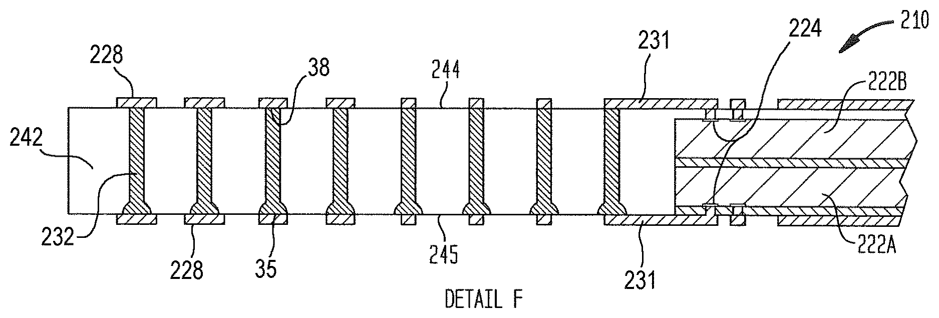
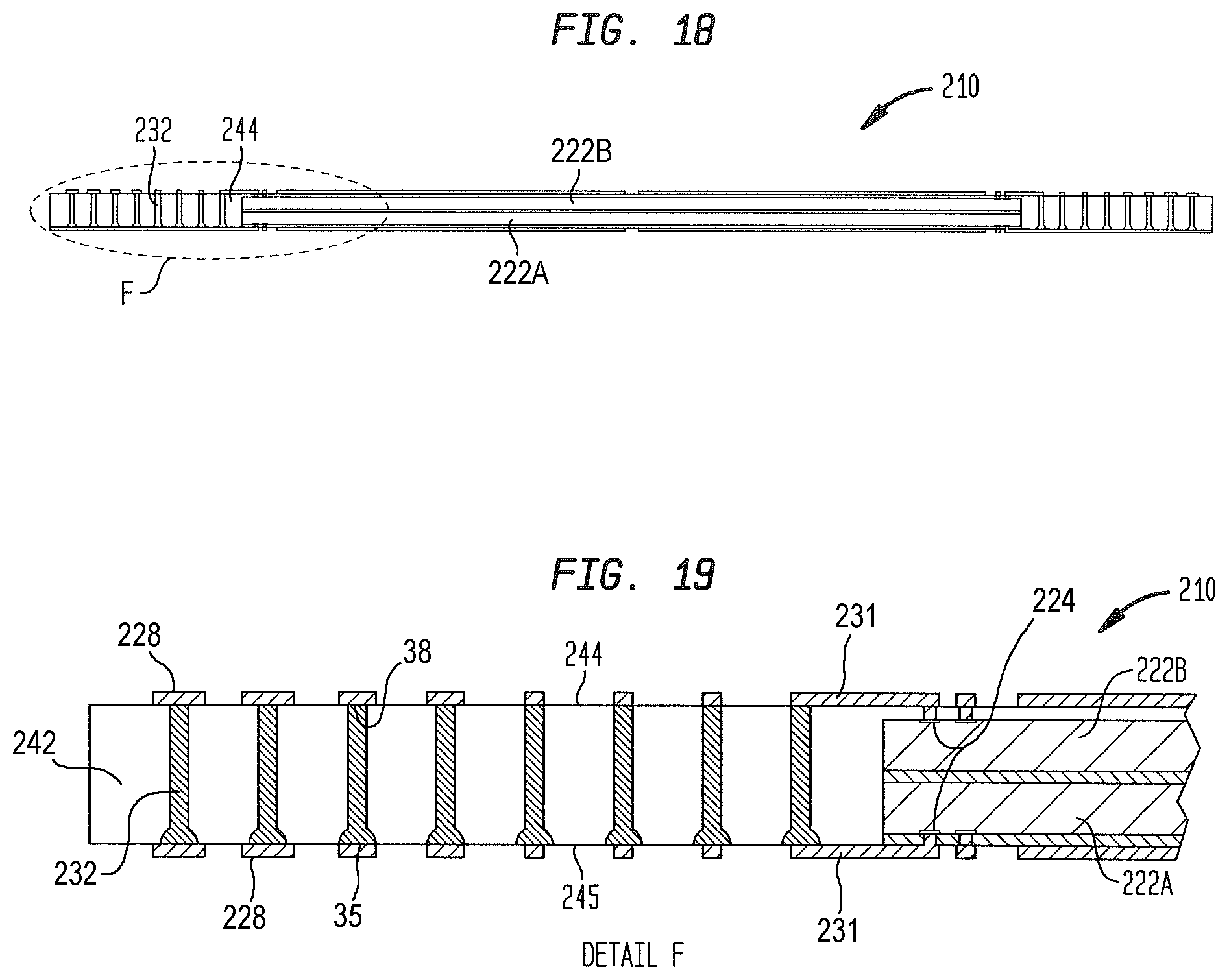
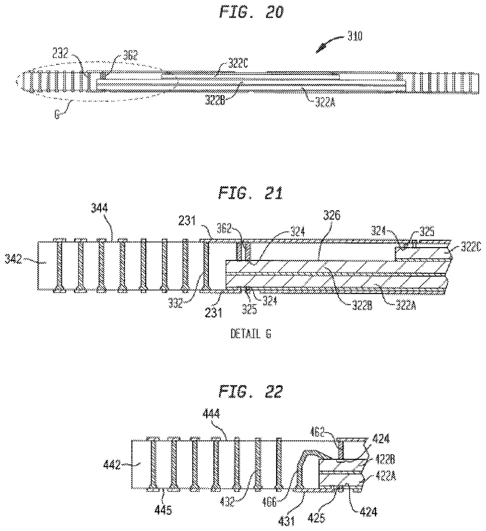
An aspect of the present disclosure relates to a method for making a microelectronic unit. The method includes forming a plurality of wire bonds on a first surface in the form of a conductive bonding surface of a structure comprising a patternable metallic element. The wire bonds are formed having bases joined to the first surface and end surfaces remote from the bases and remote from the first surface. The wire bonds further have edge surfaces extending between the bases and the end surfaces. The method also includes forming a dielectric encapsulation layer over at least a portion of the first surface of the conductive layer and over portions of the wire bonds such that unencapsulated portions of the wire bonds are defined by at least one of the end surface or a portion of the edge surface thereof that is uncovered by the encapsulation layer. Then, the metallic element is selectively patterned to form first conductive elements insulated from one another by at least portions of the encapsulation layer. At least some of the wire bonds are disposed atop the first conductive elements.
A microelectronic element can be included in the structure and electrically connected with the conductive layer when the step of removing portions of the conductive layer is performed. The step of forming the dielectric encapsulation layer can be carried out with the microelectronic element electrically connected with the conductive layer and such that the encapsulation layer at least partially covers at least one surface thereof. At least some of the first conductive elements can be electrically connected between respective ones of the wire bonds and the microelectronic element.
An example of the method can further include the step of forming a redistribution layer over the second surface of the encapsulation layer. The redistribution layer can include conductive contacts displaced in at least one lateral direction from the unexposed portions of the wire bonds.
At least some of the wire bonds can be formed such that the end surfaces thereof are displaced in one or more lateral directions from the bases thereof. In an example, the bases of the wire bonds can be arranged in a first pattern having a first minimum pitch and the unencapsulated portions of the wire bonds can be arranged in a pattern having a second minimum pitch that is greater than the first minimum pitch. Alternatively, the bases can be arranged in a first pattern having a first minimum pitch and the unencapsulated portions of the wire bonds can be arranged in a pattern having a second minimum pitch that is less than the first minimum pitch.
The method can further include forming second conductive elements overlying the second surface of the dielectric layer. At least some of the second conductive elements can be connected with respective ones of at least some of the unencapsulated portions of the wire bonds.
The step of selectively removing portions of the conductive layer can include forming at least some first conductive elements as contact pads to which bases of wire bonds that are not electrically connected with other elements of the unit are electrically connected.
The method can further include the step of thinning the unit by one of grinding or polishing. In an example, the encapsulation layer can be formed having an initial thickness such that the end surfaces of the wire bonds are substantially covered, and the step of thinning the unit can include removing a portion of the encapsulation layer such that the end surfaces become unencapsulated by the encapsulation layer.
The step of forming the encapsulation layer can include dispensing an encapsulant onto the first surface of the conductive layer and at least edge surfaces of the wire bonds. Further, the step of forming the encapsulation layer can include molding an encapsulant in contact with the conductive layer, at least edge surfaces of the wire bonds, and at least one surface of the microelectronic element.
The method can further include removing a carrier from a surface of the conductive layer opposite the wire bonds prior to performing the step of selectively removing portions of the conductive layer.
In an embodiment, the conductive layer can have a thickness of less than 20 microns.
Another aspect of the present disclosure relates to a method for making a microelectronic package. The method can include forming a plurality of wire bonds on a first surface of a conductive layer of an in process unit. The in-process unit has at least one microelectronic element joined thereto that is electrically connected with portions thereof. The wire bonds are formed having bases joined to the first surface and end surfaces remote from the bases and remote from the first surface. The wire bonds further have edge surfaces extending between the bases and the end surfaces. The method also includes forming a dielectric encapsulation layer over at least a portion of the first surface of the conductive layer, over at least a portion of the at least one microelectronic element, and over portions of the wire bonds such that unencapsulated portions of the wire bonds are defined by at least one of the end surface or a portion of the edge surface thereof that is uncovered by the encapsulation layer. Portions of the conductive layer are selectively removed to form first conductive elements thereof. At least some of the first conductive elements are electrically connected with at least some of the wire bonds, and at least some of the first conductive elements include at least some of the portions of the conductive layer with which the microelectronic element is electrically connected.
Another aspect of the present disclosure relates to a method for making a microelectronic unit. The method includes forming a plurality of wire bonds on a first surface that is a conductive bonding surface of a structure comprising a patternable metallic element. The wire bonds have bases joined to the first surface and end surfaces remote from the bases and remote from the first surface. The wire bonds further have edge surfaces extending between the bases and the end surfaces. When forming the wire bonds, the conductive layer includes a plurality of regions attached to one another at at least some edges thereof. The method also includes forming a dielectric encapsulation layer over at least a portion of the first surface of the conductive layer and over portions of the wire bonds, such that unencapsulated portions of the wire bonds are defined by at least one of the end surface or a portion of the edge surface thereof that is uncovered by the encapsulation layer, wherein when performing the step of selectively removing portions of the encapsulation layer, a plurality of microelectronic elements are joined to the conductive layer, in the form of an in-process unit having at least one microelectronic element electrically connected with each of at least some of the regions of the conductive layer. The metallic element is then selectively patterned to form first conductive elements insulated from one another by at least portions of the encapsulation layer. At least some of the wire bonds are disposed atop the first conductive elements. The in-process unit is then severed into a plurality of microelectronic units, each including the first conductive elements of a region of the conductive layer and the at least one microelectronic element electrically connected therewith.
Another aspect of the present disclosure relates to a method for making a microelectronic assembly. The method includes making a first microelectronic package, including forming a plurality of wire bonds on a first surface of a conductive layer of an in process unit. The in-process unit has at least one microelectronic element joined thereto and electrically connected with portions thereof. The wire bonds are formed having bases joined to the first surface and end surfaces remote from the bases and remote from the first surface. The wire bonds further have edge surfaces extending between the bases and the end surfaces. Forming the first microelectronic package also includes forming a dielectric encapsulation layer over at least a portion of the first surface of the conductive layer, over at least a portion of the at least one microelectronic element, and over portions of the wire bonds such that unencapsulated portions of the wire bonds are defined by at least one of the end surface or a portion of the edge surface thereof that is uncovered by the encapsulation layer. Portions of the conductive layer are then selectively removed to form first conductive elements thereof. At least some of the first conductive elements are electrically connected with at least some of the wire bonds and at least some of the first conductive elements include at least some of the portions of the conductive layer with which the microelectronic element is electrically connected. The method also includes joining the first microelectronic package with a second microelectronic package overlying the second surface of the encapsulation layer of the first package. The second microelectronic package includes a plurality of contacts exposed at a first surface thereof. Joining the first microelectronic package with the second microelectronic package includes electrically connecting the unencapsulated portions of the wire bonds of the first microelectronic package with the contacts of the second microelectronic package.
Another aspect of the present disclosure relates to a microelectronic package including at least one microelectronic element. The package further includes first electrically conductive elements including terminals exposed at a mounting surface of the package. At least some of the first conductive elements are electrically connected to the at least one microelectronic element through vias integrally formed with the first conductive elements. The package further includes wire bonds having bases joined to respective ones of the conductive elements and adjacent the first surface of the dielectric encapsulation layer and end surfaces remote from the bases. Each wire bond defines an edge surface extending between the base and the end surface thereof. The package also includes a dielectric encapsulation layer having a first surface and a second surface remote from the first surface. At least a portion of the first surface is exposed at the mounting surface of the package. The dielectric encapsulation layer fills spaces between the wire bonds such that the wire bonds are separated from one another by the encapsulation layer. Unencapsulated portions of the wire bonds are defined by at least portions of the end surfaces of the wire bonds that are uncovered by the encapsulation layer at the second surface thereof.
At least some of the unencapsulated portions of the wire bonds can be displaced in at least one lateral direction from the respective bases thereof.
The package can further include a second microelectronic element. In an example the first microelectronic element can include contacts exposed at a front face thereof that are disposed toward the first surface of the dielectric layer, and the second microelectronic element can include contacts exposed at a front face thereof that is disposed toward the second surface of the dielectric layer. In such an example, the package can further include second conductive elements exposed at the second surface of the encapsulation layer. At least some of the second conductive elements can be connected between respective ones of the contacts of the second microelectronic element and respective ones of the unencapsulated wire bond portions. The first and second microelectronic elements can be electrically connected by at least one wire bond that is electrically connected with at least one contact of the first microelectronic element and at least one contact of the second microelectronic element. Alternatively, the second microelectronic element can be connected with one of the second conductive elements by a wire bond joined between one of the contacts of the second microelectronic element and a respective one of the second microelectronic elements. In another example, the first and second microelectronic elements can be electrically connected by a wire bond joined to a contact of the second microelectronic element and a respective one of the conductive elements exposed at the first surface of the encapsulation layer.
A microelectronic assembly can include a first microelectronic package as described above and a second microelectronic package that includes a microelectronic element and terminals exposed at a surface of the second microelectronic package. The terminals can be electrically connected with the microelectronic element. Further, the second microelectronic package can overlie the first microelectronic package and can be bonded thereto with the terminals thereof electrically connected to at least some of the unencapsulated portions of the wire bonds of the first microelectronic package.
A system can include a microelectronic package, as described above and one or more electronic components.
BRIEF DESCRIPTION OF THE DRAWINGS
Various embodiments of the present invention will be now described with reference to the appended drawings. It is appreciated that these drawings depict only some embodiments of the invention and are therefore not to be considered limiting of its scope.
FIG. 1 shows a top schematic view of an in-process unit that can be processed to form a microelectronic package by steps according to a method of the present disclosure;
FIG. 2 shows a side elevation of the in-process unit of FIG. 1;
FIG. 3 shows a top view of the in-process unit of FIG. 1 in a further process step of the method;
FIG. 4 shows a side elevation view of the in-process unit of FIG. 3;
FIG. 5 shows a detail view of a portion of the in-process unit of FIG. 4 as indicated by area or detail A;
FIG. 6 shows a top view of the in-process unit of FIG. 1 in a further process step of the method;
FIG. 7 shows a side elevation view of the in-process unit of FIG. 6;
FIG. 8 shows a detail view of a portion of the in-process unit of FIG. 7 as indicated by area B or detail;
FIG. 9 shows a side elevation view of a microelectronic package that can result from the method;
FIG. 10 shows a detail view of the package of FIG. 9 as indicted by area or detail C;
FIG. 11 shows the detail view of FIG. 10 after a further optional process step of the method;
FIG. 12 shows a side view of the package of Fig.
in a further optional process step of the method;
FIG. 13 shows a detail view of a portion of the package of FIG. 11 as indicated by area or detail D;
FIG. 14 shows an alternative in-process unit that can be processed to form a microelectronic package by steps according to variation of a method of the present disclosure;
FIG. 15 shows a detail view of a portion of the in-process unit of FIG. 13 as indicated by area E;
FIG. 16 shows a side elevation view of a microelectronic package that can result from the method variation;
FIG. 17 shows a detail view of a portion of the package of FIG. 15 after an optional process step of another method variation;
FIG. 18 shows an alternative microelectronic package;
FIG. 19 shows a detail view of a portion of the package of FIG. 18 as indicated by area F;
FIG. 20 shows a further alternative microelectronic package;
FIG. 21 shows a detail view of a portion of the package of FIG. 20 as indicated by area G;
FIG. 22 shows a further alternative microelectronic package;
FIG. 23 shows a further alternative microelectronic package; and
FIG. 24 shows an example of a microelectronic assembly that can include one or more packages according to various embodiments shown herein.
FIG. 25 depicts an example of a system which may include a package according to an implementation described herein.
DETAILED DESCRIPTION
Turning now to the figures, where similar numeric references are used to indicate similar features, there is shown in FIG. 9 a microelectronic unit or package 10 according to an embodiment of the disclosure, for which FIGS. 1-8 show various stages of formation of the microelectronic package according to a method in another embodiment of the disclosure. The embodiment of FIG. 9 is a microelectronic package 10 in the form of a packaged microelectronic element such as a semiconductor chip assembly that is used in computer or other electronic applications.
The microelectronic package 10 of FIG. 9 includes a microelectronic element 22. The microelectronic package 10 can be embedded within an encapsulation layer 42 or may be contacted by the encapsulation layer at one or more surfaces thereof, e.g., a front or rear surface or an edge surface extending between the front and rear surfaces. The encapsulation layer 42 has a thickness extending from a first surface 43 or 45 to a second surface 44. The first and second surfaces can be at least partially exposed at respective first and second mounting surfaces 11 and 12 of the packages 10. Such a thickness can be at least equal to a thickness of the microelectronic element 22, itself. As seen in FIG. 10, encapsulation layer 42 can further extend outwardly from the microelectronic element 22 in lateral directions, as also shown in the plan-view of FIG. 6. A plurality of wire bonds 32 are also embedded within encapsulation layer and extend between end surfaces 35 and 38 that are respectively uncovered by the encapsulation layer and which may be flush (e.g., co-planar) with surfaces 43 or 45 and 44. For purposes of this discussion, the first surface 43 or 45 may be described as being positioned opposite or remote from second surface 44. Such a description, as well as any other description of the relative position of elements used herein that refers to a vertical or horizontal position of such elements is made for illustrative purposes only to correspond with the position of the elements within the Figures, and is not limiting.
Microelectronic element 22 can be a semiconductor chip or another comparable device having a plurality of active or passive circuit elements therein or both active and passive circuit elements which may be in the form of an integrated passives on-chip ("IPOC"), among others. In the embodiment of FIG. 10, microelectronic element 22 has at least portions of edge and rear surfaces contacted (e.g., covered by) encapsulation layer 42. The microelectronic element 22 may be positioned such that its contacts 24 are adjacent the first mounting surface 11 of the package. Further, in such an arrangement, contacts 24 are connected with conductive elements that extend along first surface 43 or 45 of encapsulation layer 42 to electrically connect with wire bonds 32 at end surfaces 35, thereof, which can be defined by bases 34 of the respective wire bonds 32. Such bases 34 can be an artifact of the process used to form wire bonds 32, and can be in the shape of such bases 34 as formed by ball bonding, as shown, or by wedge bonding, stitch bonding or the like. In other embodiments, such as that shown in FIG. 16, bases can be partially or fully removed during fabrication, such as by a thinning process of grinding, lapping, polishing, or other suitable technique. Such thinning or other process can also reduce the height of the wire bonds 132 such that end surfaces 135 are defined as extremities of the wire bonds 132 that were above the bases. In an embodiment, the microelectronic contacts 24 can be electrically connected with conductive elements 28 by conductive (e.g., metalized) vias 25 that include vias deposited onto the contacts 24 of the microelectronic element such as by plating, sputtering, or vapor deposition of one or more metals, such as one or more of copper, nickel, chromium, aluminum, gold, titanium, tungsten, cobalt, or one or more alloys thereof, without limitation. In one example, conductive elements can be formed by depositing a liquid conductive matrix material having metallic and non-metallic components, and thereafter curing the deposited conductive matrix material. For example, a conductive matrix material can be deposited and used such as described in commonly owned U.S. patent application Ser. No. 13/158,797, the disclosure of which is incorporated by reference herein.
Conductive elements 28 can include respective "contacts" or "pads" that can be exposed at the second surface of encapsulation layer 42. As used in the present description, when an electrically conductive element is described as being "exposed at" the surface of another element having dielectric structure, it indicates that the electrically conductive structure is available for contact with a theoretical point moving in a direction perpendicular to the surface of the dielectric structure toward the surface of the dielectric structure from outside the dielectric structure. Thus, a terminal or other conductive structure that is exposed at a surface of a dielectric structure may project from such surface; may be flush with such surface; or may be recessed relative to such surface and exposed through a hole or depression in the dielectric. In one example, the conductive elements 28 can be flat, thin elements that are exposed at first surface 43 of encapsulation layer 42. Conductive elements 28 can have any suitable shape and in some cases can be circular. Conductive elements 28 may be electrically interconnected with one another, to microelectronic element 22, or both, by traces 31. Conductive elements 28 can also be formed along front surface 20 of microelectronic element 22.
As shown in FIGS. 12 and 13, additional conductive elements 28 can be exposed at a second surface 44 of encapsulation layer 42. Such conductive elements 28 can overlie and electrically connect with end surfaces 38 of wire bonds 32. In other variations, such conductive elements can include pads that are displaced in at least one lateral direction along surface 44 from a corresponding wire bond, to which they can be connected at an end surface thereof by a trace 31.
Wire bonds 32 can be joined to at least some of the conductive elements 28, such as on the faces thereof. Wire bonds 32 can be joined at a base 34 thereof to the conductive elements 28 and can extend to an end 36 remote, i.e. opposite, from the respective bases 34 and from first surface 43. The ends 36 of wire bonds 32 can be characterized as being "free" in that they are not electrically connected or otherwise joined to microelectronic element 22 or any other conductive features within microelectronic package 10 that are, in turn, connected to microelectronic element 22. In other words, free ends 36 are available for electronic connection, either directly or indirectly as through a conductive element 28 or other features discussed herein, to a conductive feature external to package 10. The fact that ends 36 are held in a predetermined position by, for example, encapsulant layer 42 or otherwise joined or electrically connected to another conductive feature does not mean that they are not "free" as described herein, so long as any such feature is not electrically connected to microelectronic element 22. Conversely, bases 34 may not be free as they can be either directly or indirectly electrically connected to microelectronic element 22, as described herein. As shown in FIG. 10, bases 34 can be rounded in shape, extending outward from an edge surface 37 of wire bond 32 defined between base 34 and end 36. The particular size and shape of base 34 can vary according to the type of material used to form wire bond 32, the desired strength of the connection between wire bond 32 and conductive element 28, or the particular process used to form wire bond 32. Exemplary methods for making wire bonds 32 are described in U.S. Pat. No. 7,391,121 to Otremba, in U.S. Pat. App. Pub. No. 2005/0095835 (describing a wedge-bonding procedure that can be considered a form of wire bonding), and in commonly-assigned U.S. patent application Ser. Nos. 13/462,158; 13/404,408; 13/405,108; 13/405,125; and Ser. No. 13/404,458, the disclosures of which are incorporated herein by reference in their entireties.
Wire bonds 32 are formed by bonding a metal wire made of copper, gold, nickel, solder, aluminum, or metal alloy, among others, at a surface thereof and performing one or more other steps so as to form a wire bond having a base and an unencapsulated surface remote, e.g., opposite, therefrom with a length of the wire extending therebetween. Additionally, wire bonds 32 can be made from combinations of materials, such as from a core of a conductive material, such as copper or aluminum, for example, with a coating applied over the core. The coating can be of a second conductive material, such as aluminum, nickel, platinum, or palladium, among others. Alternatively, the coating can be of an insulating material, such as an insulating jacket. In an embodiment, the wire used to form wire bonds 32 can have a thickness, i.e., in a dimension transverse to the wire's length, of between about 15 .mu.m and 150 .mu.m. In general, wire bonds 32 can be formed on a metal bonding surface, i.e. a first metal bonding surface of a structure using a wire bond tool. In other embodiments, including those in which wedge bonding is used, such as described below, wire bonds 32 can have a thickness of up to about 500 .mu.m. A leading end of a wire segment is heated and pressed against the receiving surface to which the wire segment bonds, typically forming a ball or ball-like base 34 joined to the surface of the conductive element 28. The desired length of the wire segment to form the wire bond is drawn out of the bonding tool, which can then sever or cut the wire bond at the desired length. Wedge bonding, which can be used to form wire bonds of aluminum, for example, is a process in which the heated portion of the wire is dragged across the receiving surface to form a wedge that lies generally parallel to the surface. The wedge-bonded wire bond can then be bent upward, if necessary, and extended to the desired length or position before cutting. In a particular embodiment, the wire used to form a wire bond can be cylindrical in cross-section. Otherwise, the wire fed from the tool to form a wire bond or wedge-bonded wire bond may have a polygonal cross-section such as rectangular or trapezoidal, for example.
The free ends 36 of wire bonds 32 can define respective end surfaces 38. End surface 38 can form at least a part of a contact in a pattern such as a grid or an array formed by respective end surfaces 38 of a plurality of wire bonds 32. FIGS. 6 and 7 show an exemplary pattern for such an array of contacts formed by end surfaces 38. Such an array can be formed in an area array configuration, variations of which could be implemented using the structures described herein. In a variation of that shown, there need not be end surfaces of a wire bond at every position of the grid or array pattern in FIG. 6. Such an array can be used to electrically and mechanically connect the microelectronic package 10 to another microelectronic structure, such as to a printed circuit board ("PCB"), or to other packaged microelectronic elements, an example of which is shown in FIG. 24. In such a stacked arrangement, wire bonds 32 and conductive elements 28 can carry multiple electronic signals therethrough, each having a different signal potential to allow for different signals to be processed by different microelectronic elements in a single stack. The grid or array pattern in which end surfaces 38 are disposed at certain positions that can be disposed at positions thereof that are the same as or different than the grid or array pattern in which bases 34 are disposed. In the example shown in FIG. 9, where wire bonds 32 are generally vertically arranged, such arrays may be identical. In other arrangements, such as that shown in FIG. 23 can include wire bonds 532 that are angled 546 with respect to surface 544 of encapsulation layer 542 such that the array of end surfaces 38 has a greater pitch than that of bases 34. An inverse of such an arrangement is also possible. Further, as discussed above, conductive elements 28 can be laterally displaced from end surfaces 35 or 38 to which they are electrically connected by traces 31. This arrangement can also provide for different pitches over surfaces 544 and 545 or other different arrangements of contacts.
As shown in FIG. 24 such a package 10 can be arranged in a stack with other similar packages or the like. While FIG. 24 shows two such microelectronic packages 10A, 10B, three, four or even more can be arranged in such a stack, which can also be assembled with a circuit panel 90 with solder masses 52 joining conductive elements 28 to panel contacts 92. Solder masses 52 can also be used to interconnect the microelectronic assemblies in such a stack, such as by electronically and mechanically attaching end surfaces 38 to conductive elements 28 or connecting conductive elements 28 to other conductive elements 28.
Encapsulation layer 42 serves to protect the other elements within microelectronic package 10, particularly wire bonds 32. This allows for a more robust structure that is less likely to be damaged by testing thereof or during transportation or assembly to other microelectronic structures. Encapsulation layer 42 can be formed from a dielectric material with insulating properties such as that described in U.S. Patent App. Pub. No. 2010/0232129, which is incorporated by reference herein in its entirety.
As discussed above, FIG. 23 shows an embodiment of microelectronic assembly 510 having wire bonds 532 with ends 536 that are not positioned directly above the respective bases 34 thereof. That is, considering first surface 544 of assembly 510 as extending in two lateral directions, so as to substantially define a plane, end 536 or at least one of the wire bonds 532 is displaced in at least one of these lateral directions from a corresponding lateral position of base 34. As shown in FIG. 23, wire bonds 532 can be substantially straight along the longitudinal axis thereof, as in the embodiment of FIG. 9, with the longitudinal axis being angled at an angle 546 with respect to a first surface 544 of encapsulation layer 542. Although the cross-sectional view of FIG. 23 only shows the angle 546 through a first plane perpendicular to first surface 544, wire bond 532 can also be angled with respect to second surface 545 in another plane perpendicular to both that first plane and to second surface 545. Such an angle can be substantially equal to or different than angle 546. That is the displacement of end 536 relative to base 34 can be in two lateral directions and can be by the same or a different distance in each of those directions.
In an embodiment, various ones of wire bonds 532 can be displaced in different directions and by different amounts throughout the assembly 510. Such an arrangement allows for assembly 510 to have an array that is configured differently on the level of surface 544 compared to on the level of surface 545. For example, an array can cover a smaller overall area or have a smaller pitch on surface 544 than at the second surface 545 level. Further, some wire bonds 532 can have ends 536 that are positioned above microelectronic element 522 to accommodate a stacked arrangement of packaged microelectronic elements of different sizes. In another embodiment, wire bonds can achieve this lateral displacement by including curved portions therein. Such curved portions can be formed in an additional step during the wire bond formation process and can occur, for example, while the wire portion is being drawn out to the desired length. This step can be carried out using available wire-bonding equipment, which can include the use of a single machine. Such curved portions can take on a variety of shapes, as needed, to achieve the desired positions of the ends of the wire bonds. For example, curved portions can be formed as S-curves of various shapes.
FIGS. 1-8 show a microelectronic package 10 in various steps of a fabrication method thereof. FIGS. 1 and 2 show microelectronic package 10 at a step where microelectronic element 22 has been bonded to a structure comprising a patternable metallic element 28'. The structure may include or consist of a metallic or other electrically conductive material layer extending in first and second transverse directions 15, 17 to define a general shape of package 10, as can be seen in the plan view of FIG. 1. Microelectronic element 22 can be assembled, e.g., bonded, to the conductive material layer 28' using an adhesive layer or polymeric material which is not fully cured. In some embodiments, the structure may include a support layer or device, e.g., a carrier to support the conductive material layer 28' during at least some steps during fabrication. Such a support layer can be removed after formation of the encapsulation layer 42.
FIGS. 3, 4 and 5 show microelectronic package 10 having wire bonds 32 joined at predetermined locations on surface 30' of conductive material layer 28'. As discussed, wire bonds 32 can be applied by heating an end of a wire segment to soften the end such that it forms a deposition bond to conductive element 28 when pressed thereto, forming base 34. The wire is then drawn out away from conductive element 28 and manipulated, if desired, in a specified shape before being severed to form end 36 and end surface 38 of wire bond 32. Alternatively, wire bonds 32 can be formed from, for example, an aluminum wire by wedge bonding. Wedge bonding is formed by heating a portion of the wire adjacent the end thereof and dragging it along the conductive element 28 with pressure applied thereto. Such a process is described further in U.S. Pat. No. 7,391,121, the disclosure of which is hereby incorporated by reference herein in its entirety, and in previously-referenced U.S. patent application Ser. No. 13/402,158.
In FIGS. 6-8 encapsulation layer 42 has been added to microelectronic package 10 by being applied over surface 30' of conductive material layer 28', extending upwardly therefrom and along edge surfaces 37 of wire bonds 32. Encapsulation layer 42 can also extend along at least a portion of microelectronic element 22, including over at least one of the front face, rear face, or edge surface thereof. In other examples, the encapsulation layer 42 can be formed such that it does not contact any portions of microelectronic element 22, such as by being laterally spaced away therefrom. Encapsulation layer 42 can be formed by depositing an encapsulant, e.g., a resin over the stage of microelectronic package 10 shown in FIG. 4. In one example, this can be done by placing package 10 in an appropriately configured mold having a cavity in the desired shape of the encapsulation layer 42 that can receive package 10. Such a mold and the method of forming an encapsulation layer therewith can be as shown and described in U.S. Pat. App. Pub. No 2010/0232129, the disclosure of which is incorporated by reference herein it its entirety. Alternatively, encapsulation layer 42 can be prefabricated to the desired shape from an at least partially compliant material. In this configuration, compliant properties of the dielectric material allow encapsulation layer 42 to be pressed into position over wire bonds 32 and microelectronic element 22. In such a step, wire bonds 32 penetrate into the compliant material forming respective holes therein, along which encapsulation layer 42 contacts edge surfaces 37. Further, microelectronic element 22 may deform the compliant material so that it can be received therein. The compliant dielectric material can be compressed to expose end surfaces 38 on outer surface 44. Alternatively, any excess compliant dielectric material can be removed from encapsulation layer to form a surface 44 on which end surfaces 38 of wire bonds 32 are uncovered.
In an example, the encapsulation layer 42 can be formed such that, initially, surface 44 thereof is spaced above end surfaces 38 of wire bonds 32. To expose the end surfaces 38, the portion of encapsulation layer 42 that is above end surfaces 38 can be removed, exposing a new surface 44 that is substantially flush with end surfaces 38, as shown in FIG. 7. In a further alternative, encapsulation layer 42 can be formed such that surface 44 is already substantially flush with end surfaces 38 or such that surface 44 is positioned below end surfaces 38. Removal, if necessary, of a portion of encapsulation layer 42 can be achieved by grinding, dry etching, laser etching, wet etching, lapping, or the like. If desired, a portion of the ends 36 of wire bonds 32 can also be removed in the same, or an additional, step to achieve substantially planar end surface 38 that are substantially flush with surface 44. In a particular example, the encapsulation can be applied over the microelectronic element 22, wire bonds 34, and patternable conductive element 28' without using a mold and excess encapsulant can be removed after the application thereof to expose the end surfaces of the wire bonds, e.g., by polishing or one or more of the above methods.
After formation of dielectric layer 42, conductive material layer 28' can be patterned, by chemical or mechanical etching (such as laser etching or the like), to make conductive elements 28 and/or traces 31 by removing portions of conductive material layer 28' and leaving the portions thereof in the desired locations and form of the desired conductive elements 28 or traces 31. This can be done to make selective interconnections between wire bonds 32 and contacts 24 of microelectronic element 22 or to form conductive elements 28 displaced from respective wire bonds 32 with which they can be connected by traces 31. In some embodiments, conductive vias 25 can be formed to connect traces 31 or conductive features 28 in the form of pads with the microelectronic contacts 24.
As shown in FIG. 11, the package 10 can then be thinned to planarize surface 44 and end surfaces 38 of wire bonds 32. This can include exposing a surface of microelectronic element 22 on surface 44, which can also include thinning of microelectronic element 22 itself. Additionally or alternatively, conductive features 28 and/or traces 31 can be formed over surface 44, as described above. This can be done by depositing or joining a conductive layer over surface 44 and then patterning the layer to form such conductive elements 28 and traces 31.
FIGS. 16 and 17 show a microelectronic package 110 that is similar in construction to that shown in FIG. 10 but with microelectronic element 122 in a "face-up" arrangement. In such an arrangement, microelectronic contacts 124 are disposed toward surface 144 of encapsulation layer 142. Further, microelectronic element 122 can connect with the pattern of wire bonds 132 by conductive features 128 and traces 131 that are exposed at surface 144. As shown in FIGS. 16 and 17, such traces 131 and conductive elements 128 can connect with microelectronic contacts 124 by metalized vias 125 that extend from surface 144 to the contacts 124.
As illustrated in FIG. 16, the routing achieved by traces 131 and conductive elements 128 exposed on surface 144 can be the only routing in package 110, with surface 145 being ground down to remove conductive material layer 128' (FIG. 15), which can also remove further encapsulation material, bases 134, and all or a portion of the attachment layer 120.
Alternatively, as shown in FIG. 16 electrically conductive routing elements can also be included on surface 145 that can be for purposes or redistribution of wettable contacts in the array over surface 145. In other examples, a designated wire bond can connect with the microelectronic element 122 by routing over surface 144, which can, in turn connect with other wire bonds by routing over surface 145 that is connected with such designated wire bonds.
FIGS. 14 and 15 show microelectronic package 110 in process steps that can lead to either of the completed packages 110 shown in FIGS. 16 and 17. Specifically, FIGS. 14 and 15 show package 110 with microelectronic element 122 bonded, face-up, on conductive material layer 128'. Similarly, wire bonds 132 have been joined to surface 130' of conductive material layer 128' and formed according to any one of the processes described above. Further, encapsulation layer 142 has been deposited over exposed portions of surface 130' and over wire bonds 132 and microelectronic element 122, according to any of the various processes described above. Routing circuitry in the form of conductive elements 128 and traces 131 were then formed over surface 144 of encapsulation layer 142 to connect wire bonds 132 with microelectronic element 122.
At such a point, package 110 can be further processed by grinding, polishing, lapping or other techniques as described above to remove material to result in the package 110 shown in FIG. 16. Alternatively, additional routing can be formed by patterning conductive material layer 128' to form conductive elements 128 and traces 131 in the desired configuration, as described above with respect to FIGS. 9 and 10.
FIGS. 18-22 show various arrangements of packages of a similar general structure to those described above but utilizing multiple microelectronic elements. In one example, FIGS. 18 and 19 show a microelectronic package 210 having one microelectronic element 222A embedded within encapsulation layer 242 in a face-down arrangement and another microelectronic element 222B in a face-up arrangement. Such a package 210 can utilize electrically conductive routing circuitry in the form of interconnected conductive elements 228 and traces 231 over both surface 244 and surface 245 of encapsulation layer 242. Additionally, designated wire bonds 232 can be used to electrically connect microelectronic element 222A with microelectronic element 222B by routing circuitry that connects with such a designated wire bond over each end surface 35 and 38 and respectively to at least one contact 224 of each of microelectronic elements 222A and 222B. Such a package 210 can be made by a method that is similar to those described above with respect to FIGS. 1-16.
FIGS. 20 and 21 show an arrangement of a microelectronic package 310 that is similar to that shown in FIGS. 18 and 19, but with an additional microelectronic element 322C in a face-up arrangement bonded over face 326 of microelectronic element 322B. To facilitate connection of microelectronic element 322B to electrically conductive routing circuitry over surface 344, microelectronic element 322C can be smaller than microelectronic element 322B or can be offset therefrom such that contacts 324 of microelectronic element 322B are uncovered by microelectronic element 322C. Such a connection can be achieved by metalized vias 325 that connect with the element contacts 324 or by additional wire bonds 362 that are joined to contacts 324 of microelectronic element 322B and are uncovered by encapsulation layer 342 on surface 344. As discussed above, routing between any of the microelectronic element 322A, 322B, and 322C can be achieved by designated wire bonds 332 with appropriately configured routing circuitry connected therewith.
In a further example shown in FIG. 22, a microelectronic package can be similar to that shown in FIGS. 18 and 19, but with additional wire bonds 466 that connect between one or more contacts 424 of microelectronic element 422B (which are disposed toward surface 444 of encapsulation layer 442) and a portion of the routing circuitry over surface 445 of encapsulation layer 442. In the example shown, such a wire bond 466 can be used to achieve a connection between microelectronic element 422B and microelectronic element 422A, which has contacts 424 disposed toward surface 445 of encapsulation layer 442. As shown wire bond 466, or 462, can join with a trace 431 (or a conductive element, if desired) that is further connected to a metalized via 425 that electrically connects with element contacts 424 of microelectronic element 422A, or 422B.
The structures discussed above can be utilized in construction of diverse electronic systems. For example, a system 611 in accordance with a further embodiment includes microelectronic package 610, as described above, in conjunction with other electronic components 613 and 615. In the example depicted, component 613 is a semiconductor chip whereas component 615 is a display screen, but any other components can be used. Of course, although only two additional components are depicted in FIG. 25 for clarity of illustration, the system may include any number of such components. The microelectronic package 610 as described above may be, for example, a microelectronic package as discussed above in connection with FIG. 10, or a structure incorporating plural microelectronic packages as discussed with reference to FIG. 24. Package 610 can further include any one of the embodiments described in FIGS. 13-23. In a further variant, multiple variations may be provided, and any number of such structures may be used.
Microelectronic package 610 and components 613 and 615 are mounted in a common housing 619, schematically depicted in broken lines, and are electrically interconnected with one another as necessary to form the desired circuit. In the exemplary system shown, the system includes a circuit panel 617 such as a flexible printed circuit board, and the circuit panel includes numerous conductors 621, of which only one is depicted in FIG. 25, interconnecting the components with one another. However, this is merely exemplary; any suitable structure for making electrical connections can be used.
The housing 619 is depicted as a portable housing of the type usable, for example, in a cellular telephone or personal digital assistant, and screen 615 is exposed at the surface of the housing. Where microelectronic package 610 includes a light-sensitive element such as an imaging chip, a lens 811 or other optical device also may be provided for routing light to the structure. Again, the simplified system shown in FIG. 25 is merely exemplary; other systems, including systems commonly regarded as fixed structures, such as desktop computers, routers and the like can be made using the structures discussed above.
Although the invention herein has been described with reference to particular embodiments, it is to be understood that these embodiments are merely illustrative of the principles and applications of the present invention. It is therefore to be understood that numerous modifications may be made to the illustrative embodiments and that other arrangements may be devised without departing from the spirit and scope of the present invention as defined by the appended claims.
* * * * *
References
D00000
D00001
D00002
D00003
D00004
D00005
D00006
D00007
D00008
D00009
D00010
D00011
XML
uspto.report is an independent third-party trademark research tool that is not affiliated, endorsed, or sponsored by the United States Patent and Trademark Office (USPTO) or any other governmental organization. The information provided by uspto.report is based on publicly available data at the time of writing and is intended for informational purposes only.
While we strive to provide accurate and up-to-date information, we do not guarantee the accuracy, completeness, reliability, or suitability of the information displayed on this site. The use of this site is at your own risk. Any reliance you place on such information is therefore strictly at your own risk.
All official trademark data, including owner information, should be verified by visiting the official USPTO website at www.uspto.gov. This site is not intended to replace professional legal advice and should not be used as a substitute for consulting with a legal professional who is knowledgeable about trademark law.