Dual lead frame semiconductor package and method of manufacture
Kuo , et al.
U.S. patent number 10,229,893 [Application Number 15/457,790] was granted by the patent office on 2019-03-12 for dual lead frame semiconductor package and method of manufacture. This patent grant is currently assigned to VISHAY-SILICONIX. The grantee listed for this patent is VISHAY-SILICONIX. Invention is credited to Suresh Belani, Frank Kuo.


View All Diagrams
| United States Patent | 10,229,893 |
| Kuo , et al. | March 12, 2019 |
Dual lead frame semiconductor package and method of manufacture
Abstract
A semiconductor package and a method for making the same are provided. In the method, a clip is used to conduct a lead frame and at least one chip. The clip has at least one second connection segment, at least one third connection segment, and at least one intermediate connection segment. The second connection segment is electrically connected to a second conduction region of the chip and a second pin of the lead frame respectively, and the third connection segment is electrically connected to a third conduction region of the chip and a third pin of the lead frame respectively. The intermediate connection segment connects the at least one second connection segment and the at least one third connection segment, and is removed in a subsequent process. Thereby, the present invention does not need to use any gold wire, which effectively saves the material cost and the processing time.
| Inventors: | Kuo; Frank (Kaohsiung, TW), Belani; Suresh (Los Altos, CA) | ||||||||||
|---|---|---|---|---|---|---|---|---|---|---|---|
| Applicant: |
|
||||||||||
| Assignee: | VISHAY-SILICONIX (San Jose,
CA) |
||||||||||
| Family ID: | 46018822 | ||||||||||
| Appl. No.: | 15/457,790 | ||||||||||
| Filed: | March 13, 2017 |
Prior Publication Data
| Document Identifier | Publication Date | |
|---|---|---|
| US 20170271304 A1 | Sep 21, 2017 | |
Related U.S. Patent Documents
| Application Number | Filing Date | Patent Number | Issue Date | ||
|---|---|---|---|---|---|
| 14474420 | Sep 2, 2014 | 9595503 | |||
| 13229667 | Sep 2, 2014 | 8822273 | |||
| Current U.S. Class: | 1/1 |
| Current CPC Class: | H01L 21/56 (20130101); H01L 24/41 (20130101); H01L 24/84 (20130101); H01L 23/4952 (20130101); H01L 24/36 (20130101); H01L 21/78 (20130101); H01L 24/83 (20130101); H01L 24/33 (20130101); H01L 24/34 (20130101); H01L 24/40 (20130101); H01L 21/4825 (20130101); H01L 24/90 (20130101); H01L 24/97 (20130101); H01L 23/49575 (20130101); H01L 23/49562 (20130101); H01L 24/38 (20130101); H01L 23/49524 (20130101); H01L 24/32 (20130101); H01L 2224/48247 (20130101); H01L 2924/01082 (20130101); H01L 2924/01033 (20130101); H01L 2224/40095 (20130101); H01L 2924/14 (20130101); H01L 2224/37013 (20130101); H01L 2924/01006 (20130101); H01L 2224/40247 (20130101); H01L 2224/32245 (20130101); H01L 2924/1306 (20130101); H01L 2224/45144 (20130101); H01L 2224/84801 (20130101); H01L 24/49 (20130101); H01L 2224/4103 (20130101); H01L 2924/13091 (20130101); H01L 2224/83801 (20130101); H01L 24/45 (20130101); H01L 2224/97 (20130101); H01L 2924/00012 (20130101); H01L 2924/181 (20130101); H01L 2224/49111 (20130101); H01L 2924/01079 (20130101); H01L 2224/83 (20130101); H01L 2924/00014 (20130101); H01L 2224/40245 (20130101); H01L 2924/00015 (20130101); H01L 24/48 (20130101); H01L 2924/01005 (20130101); H01L 2924/014 (20130101); H01L 2224/97 (20130101); H01L 2224/84 (20130101); H01L 2224/97 (20130101); H01L 2224/83 (20130101); H01L 2224/49111 (20130101); H01L 2224/48247 (20130101); H01L 2924/00 (20130101); H01L 2924/00015 (20130101); H01L 2224/45144 (20130101); H01L 2224/48247 (20130101); H01L 2924/13091 (20130101); H01L 2224/45144 (20130101); H01L 2924/00014 (20130101); H01L 2924/1306 (20130101); H01L 2924/00 (20130101); H01L 2224/45144 (20130101); H01L 2924/00 (20130101); H01L 2224/45144 (20130101); H01L 2924/00015 (20130101); H01L 2924/181 (20130101); H01L 2924/00 (20130101); H01L 2924/181 (20130101); H01L 2924/00012 (20130101); H01L 2924/14 (20130101); H01L 2924/00 (20130101); H01L 2224/84801 (20130101); H01L 2924/00014 (20130101); H01L 2924/00014 (20130101); H01L 2224/37099 (20130101); H01L 2224/83801 (20130101); H01L 2924/00014 (20130101) |
| Current International Class: | H01L 23/00 (20060101); H01L 23/495 (20060101); H01L 21/78 (20060101); H01L 21/48 (20060101); H01L 21/56 (20060101) |
References Cited [Referenced By]
U.S. Patent Documents
| 5098626 | March 1992 | Pas |
| 5304831 | April 1994 | Yilmaz et al. |
| 5316959 | May 1994 | Kwan et al. |
| 5430324 | July 1995 | Bencuya |
| 5608260 | March 1997 | Carper et al. |
| 5710064 | January 1998 | Song et al. |
| 5804468 | September 1998 | Tsuji et al. |
| 6028352 | February 2000 | Eide |
| 6246115 | June 2001 | Tang et al. |
| 6274905 | August 2001 | Mo |
| 6285058 | September 2001 | Narazaki et al. |
| 6285075 | September 2001 | Combs et al. |
| 6307755 | October 2001 | Williams et al. |
| 6319828 | November 2001 | Jeong et al. |
| 6351018 | February 2002 | Sapp |
| 6429481 | August 2002 | Mo et al. |
| 6432750 | August 2002 | Jeon et al. |
| 6475834 | November 2002 | Embong et al. |
| 6580161 | June 2003 | Kobayakawa |
| 6613607 | September 2003 | Janssen et al. |
| 6652799 | November 2003 | Seng et al. |
| 6654248 | November 2003 | Fishley et al. |
| 6700793 | March 2004 | Takagawa et al. |
| 6777800 | August 2004 | Madrid et al. |
| 6849930 | February 2005 | Nakajima et al. |
| 6873041 | March 2005 | Crowley et al. |
| 6891256 | May 2005 | Joshi et al. |
| 7071033 | July 2006 | Estacio |
| 7132734 | November 2006 | Johnson |
| 7238551 | July 2007 | Kasem et al. |
| 7271470 | September 2007 | Otremba |
| 7271477 | September 2007 | Saito et al. |
| 7394150 | July 2008 | Kasem et al. |
| 7595017 | September 2009 | Siegel et al. |
| 7768108 | August 2010 | Liu et al. |
| 7842541 | November 2010 | Rusli et al. |
| 7902646 | March 2011 | Liu et al. |
| 8018054 | September 2011 | Liu et al. |
| 8026589 | September 2011 | Kim et al. |
| 8358014 | January 2013 | Koduri |
| 8358017 | January 2013 | Tsui |
| 8426952 | April 2013 | Cho et al. |
| 8461669 | June 2013 | Yang et al. |
| 8513784 | August 2013 | Lu et al. |
| 8581376 | November 2013 | Yilmaz et al. |
| 8586419 | November 2013 | Jaunay et al. |
| 8604597 | December 2013 | Jiang |
| 8822273 | September 2014 | Kuo et al. |
| 8952509 | February 2015 | Yilmaz et al. |
| 8958509 | February 2015 | Wiegand |
| 9024423 | May 2015 | Muto et al. |
| 9048338 | June 2015 | Hosseini et al. |
| 9184152 | November 2015 | Kuo et al. |
| 9425305 | August 2016 | Terrill et al. |
| 9595503 | March 2017 | Kuo |
| 9966330 | May 2018 | Terrill et al. |
| 2001/0000924 | May 2001 | Karnezos et al. |
| 2001/0052641 | December 2001 | Kuo et al. |
| 2003/0042556 | March 2003 | Gajda et al. |
| 2004/0063240 | April 2004 | Madrid et al. |
| 2004/0070352 | April 2004 | Shen |
| 2004/0157372 | August 2004 | Manatad |
| 2004/0188699 | September 2004 | Kameyama et al. |
| 2004/0256703 | December 2004 | Tu et al. |
| 2005/0077617 | April 2005 | Hirano et al. |
| 2005/0139982 | June 2005 | Fukaya et al. |
| 2005/0146058 | July 2005 | Danno |
| 2005/0260404 | November 2005 | Iwade et al. |
| 2006/0017143 | January 2006 | Shimanuki et al. |
| 2006/0169796 | August 2006 | Timpson et al. |
| 2006/0169976 | August 2006 | Kameda et al. |
| 2007/0096337 | May 2007 | Choi |
| 2007/0108575 | May 2007 | Montgomery |
| 2007/0114352 | May 2007 | Cruz et al. |
| 2007/0132073 | June 2007 | Tiong et al. |
| 2007/0132079 | June 2007 | Otremba et al. |
| 2007/0262346 | November 2007 | Otremba et al. |
| 2007/0278571 | December 2007 | Bhalla et al. |
| 2008/0048301 | February 2008 | Wang et al. |
| 2008/0122071 | May 2008 | Tseng et al. |
| 2008/0211070 | September 2008 | Sun et al. |
| 2008/0217753 | September 2008 | Otani |
| 2008/0233679 | September 2008 | Luo et al. |
| 2008/0246130 | October 2008 | Carney et al. |
| 2009/0008759 | January 2009 | Yoshino |
| 2009/0039484 | February 2009 | Mahler |
| 2009/0057852 | March 2009 | Madrid |
| 2009/0057855 | March 2009 | Quinones et al. |
| 2009/0057869 | March 2009 | Hebert et al. |
| 2009/0108467 | April 2009 | Otremba |
| 2009/0121331 | May 2009 | Cruz |
| 2009/0130799 | May 2009 | Havanur |
| 2009/0224383 | September 2009 | Cruz et al. |
| 2009/0294934 | December 2009 | Shi et al. |
| 2010/0133670 | June 2010 | Liu et al. |
| 2010/0148346 | June 2010 | Quinones et al. |
| 2010/0164078 | July 2010 | Madrid et al. |
| 2010/0171543 | July 2010 | Korec et al. |
| 2010/0295160 | November 2010 | Liu et al. |
| 2010/0301496 | December 2010 | Koduri |
| 2011/0024917 | February 2011 | Bhalla et al. |
| 2011/0074016 | March 2011 | Narita |
| 2011/0089485 | April 2011 | Gao et al. |
| 2011/0095411 | April 2011 | Herbsommer et al. |
| 2011/0108965 | May 2011 | Hess et al. |
| 2011/0175217 | July 2011 | Jaunay et al. |
| 2011/0198739 | August 2011 | Amanai et al. |
| 2011/0210406 | September 2011 | Terrill et al. |
| 2011/0227207 | September 2011 | Yilmaz et al. |
| 2011/0316135 | December 2011 | Urushihata |
| 2011/0316156 | December 2011 | Pagaila et al. |
| 2012/0049336 | March 2012 | Xue et al. |
| 2012/0112331 | May 2012 | Kuo et al. |
| 2012/0119343 | May 2012 | Bayan et al. |
| 2012/0126323 | May 2012 | Wu et al. |
| 2012/0146202 | June 2012 | Xue et al. |
| 2012/0181674 | July 2012 | Cho et al. |
| 2012/0200281 | August 2012 | Herbsommer et al. |
| 2012/0248539 | October 2012 | Zhang et al. |
| 2012/0280308 | November 2012 | Disney |
| 2012/0292753 | November 2012 | Cho |
| 2012/0326287 | December 2012 | Joshi et al. |
| 2013/0113114 | May 2013 | Hosseini et al. |
| 2013/0221511 | August 2013 | Higgins, III et al. |
| 2013/0256852 | October 2013 | Wyant et al. |
| 2014/0061884 | March 2014 | Carpenter et al. |
| 2014/0063744 | March 2014 | Lopez et al. |
| 2014/0077352 | March 2014 | Leal et al. |
| 2014/0084429 | March 2014 | Chen et al. |
| 2014/0117523 | May 2014 | Ho et al. |
| 2014/0191334 | July 2014 | Xue et al. |
| 2014/0264611 | September 2014 | Lee et al. |
| 2014/0264804 | September 2014 | Terrill et al. |
| 2014/0273344 | September 2014 | Terrill et al. |
| 2014/0370661 | December 2014 | Kuo et al. |
| 2015/0001618 | January 2015 | Hebert |
| 2015/0035129 | February 2015 | Zhang et al. |
| 2016/0093560 | March 2016 | Huo et al. |
| 2016/0118320 | April 2016 | Coppone et al. |
| 2016/0260697 | September 2016 | Cho et al. |
| 2017/0162403 | June 2017 | Terrill et al. |
| 100435324 | Nov 2008 | CN | |||
| 102714201 | Oct 2012 | CN | |||
| 102012110494 | May 2013 | DE | |||
| 1009035 | Jun 2000 | EP | |||
| 2477221 | Jul 2012 | EP | |||
| 2002217416 | Aug 2002 | JP | |||
| 2006216940 | Aug 2006 | JP | |||
| 2008235589 | Oct 2008 | JP | |||
| 2010034350 | Feb 2010 | JP | |||
| 2010109255 | May 2010 | JP | |||
| 2010283236 | Dec 2010 | JP | |||
| 2013508980 | Mar 2013 | JP | |||
| 1020110097925 | Aug 2011 | KR | |||
| 1020120125462 | Nov 2012 | KR | |||
| 200949966 | Dec 2009 | TW | |||
| 9965062 | Dec 1999 | WO | |||
Other References
|
Kyle Terrill et al., U.S. Appl. No. 13/830,041, "Methodfor Fabricating Stack Die Package", filed Mar. 14, 2013. cited by applicant. |
Primary Examiner: Dulka; John P.
Parent Case Text
RELATED APPLICATION(S)
This is a continuation of U.S. patent application Ser. No. 14/474,420, now U.S. Pat. No. 9,595,503, filed Sep. 2, 2014, which is incorporated by reference herein in its entirety.
Claims
What is claimed is:
1. A semiconductor package, comprising: a substrate lead frame configured for mounting a first face of an integrated circuit chip, and further configured to couple a plurality of electrical signals of said integrated circuit chip to an exterior of said semiconductor package; a clip lead frame comprising: a first clip lead portion configured to couple a first conductive region of said integrated circuit chip to a first portion of said substrate lead frame; and a second clip lead portion configured to couple a second conductive region of said integrated circuit chip to a second portion of said substrate lead frame, wherein said substrate lead frame comprises the same material as said clip lead frame.
2. The semiconductor package of claim 1, wherein the first and second conductive regions of said integrated circuit chip are on an opposite face of said integrated circuit chip from said first face.
3. The semiconductor package of claim 1, wherein each of said first and second portions of said clip lead frame are non-planar.
4. The semiconductor package of claim 1, wherein said clip lead frame comprises the same material as said substrate lead frame.
5. The semiconductor package of claim 1, wherein said clip lead frame is free of gold.
6. The semiconductor package of claim 1, wherein said semiconductor package is free of wire bonds.
7. The semiconductor package of claim 1, wherein said first clip lead portion is configured to couple to a source contact of said integrated circuit chip, and said second clip lead portion is configured to couple to a gate contact of said integrated circuit chip.
8. A semiconductor package comprising: an integrated circuit chip comprising first and second opposing faces, wherein said first face is electrically and mechanically coupled to a substrate lead frame, and wherein said substrate lead frame couples a plurality of electrical signals of said integrated circuit chip to an exterior of said semiconductor package; a clip lead frame comprising: a first clip lead portion coupling a first conductive region of said integrated circuit chip to a first portion of said substrate lead frame; and a second clip lead portion coupling a second conductive region of said integrated circuit chip to a second portion of said substrate lead frame, wherein said clip lead frame consists of metal.
9. The semiconductor package of claim 8, wherein the first and second conductive regions of said integrated circuit chip are on said second face of said integrated circuit chip.
10. The semiconductor package of claim 8, wherein said first portion of said clip lead frame is non-planar.
11. The semiconductor package of claim 8, wherein said clip lead frame comprises the same material as said substrate lead frame.
12. The semiconductor package of claim 8, wherein said clip lead frame is free of gold.
13. The semiconductor package of claim 8, wherein said semiconductor package is free of wire bonds.
14. The semiconductor package of claim 8, wherein said first clip lead portion is configured to couple to a source contact of said integrated circuit chip, and said second clip lead portion is configured to couple to a gate contact of said integrated circuit chip.
15. A clip lead frame comprising: a single contiguous piece of electrically conductive material comprising: a plurality of first clip lead portions configured to couple a first conductive region of an integrated circuit chip to a first portion of a substrate lead frame; a plurality of second clip lead portions configured to couple a second conductive region of said integrated circuit chip to a second portion of said substrate lead frame; and a plurality of clip lead frame extensions coupled to said plurality of first clip lead portions and further coupled to said plurality of second clip lead portions.
16. The clip lead frame of claim 15 wherein said clip lead frame is non-planar.
17. The clip lead frame of claim 15 comprising one or more larger physical areas for providing an area required by absorption.
18. The clip lead frame of claim 15 wherein each of said first clip lead portions comprises a first clip lead portion end configured for solder reflow bonding to said first conductive region.
19. The clip lead frame of claim 15 wherein each of said first clip lead portions comprises a second clip lead recess portion configured for solder reflow bonding to said substrate lead frame.
20. The clip lead frame of claim 15 wherein said clip lead frame is free of structures joining materials together.
Description
BACKGROUND
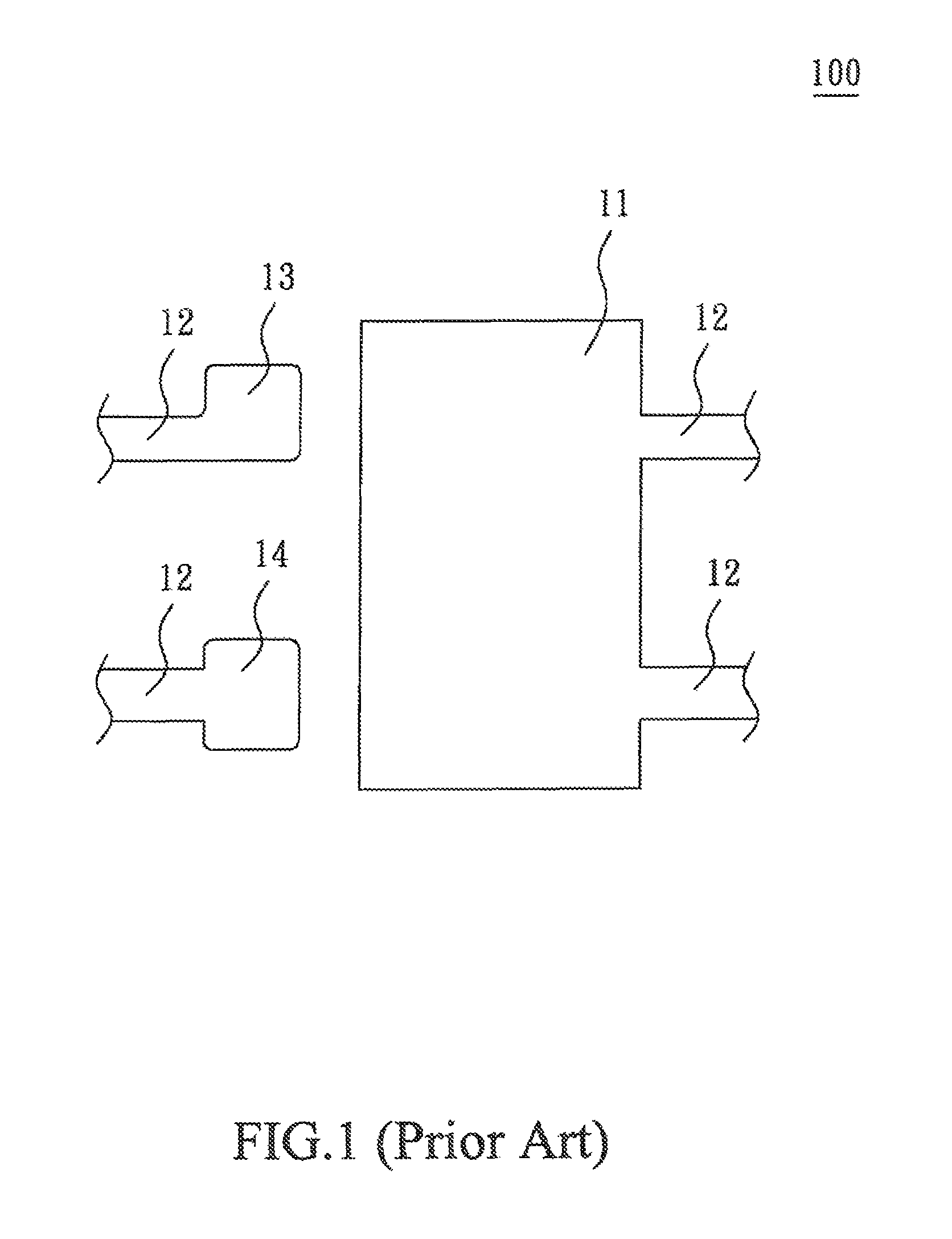
The manufacture of integrated circuits includes the packaging of the semiconductor chip. FIGS. 1, 2 and 3 illustrate a conventional method for making a semiconductor package. Referring to FIG. 1, a lead frame is provided. The lead frame 1 includes at least one drain pin 11, at least one source pin 13 and at least one gate pin 14. The drain pin 11, source pin 13 and gate pin are connected to a frame (not shown) by corresponding extensions 12. The source pin 13 and the gate pin 14 face a side of the drain pin 11, and a space exists between the source pin 13 and the side of the drain pin 11 and between the gate pin 14 and the side of the drain pin 11.
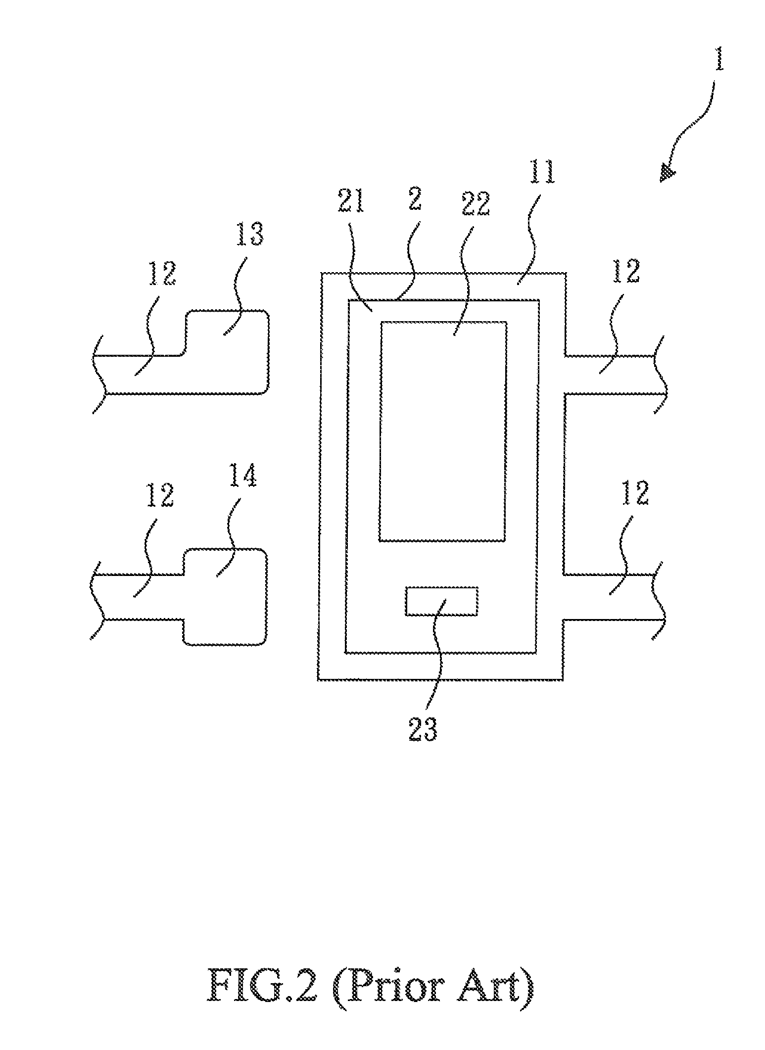
Referring now to FIG. 2, at least one chip 2 is provided. The chip 2 has an upper surface 21 and a lower surface (not shown). The upper surface 21 has a source conductive region 22 and a gate conductive region 23. The lower surface has a drain conductive region (not shown). The chip 2 is disposed so that the drain conductive region is electrically connected to the drain pin 11.
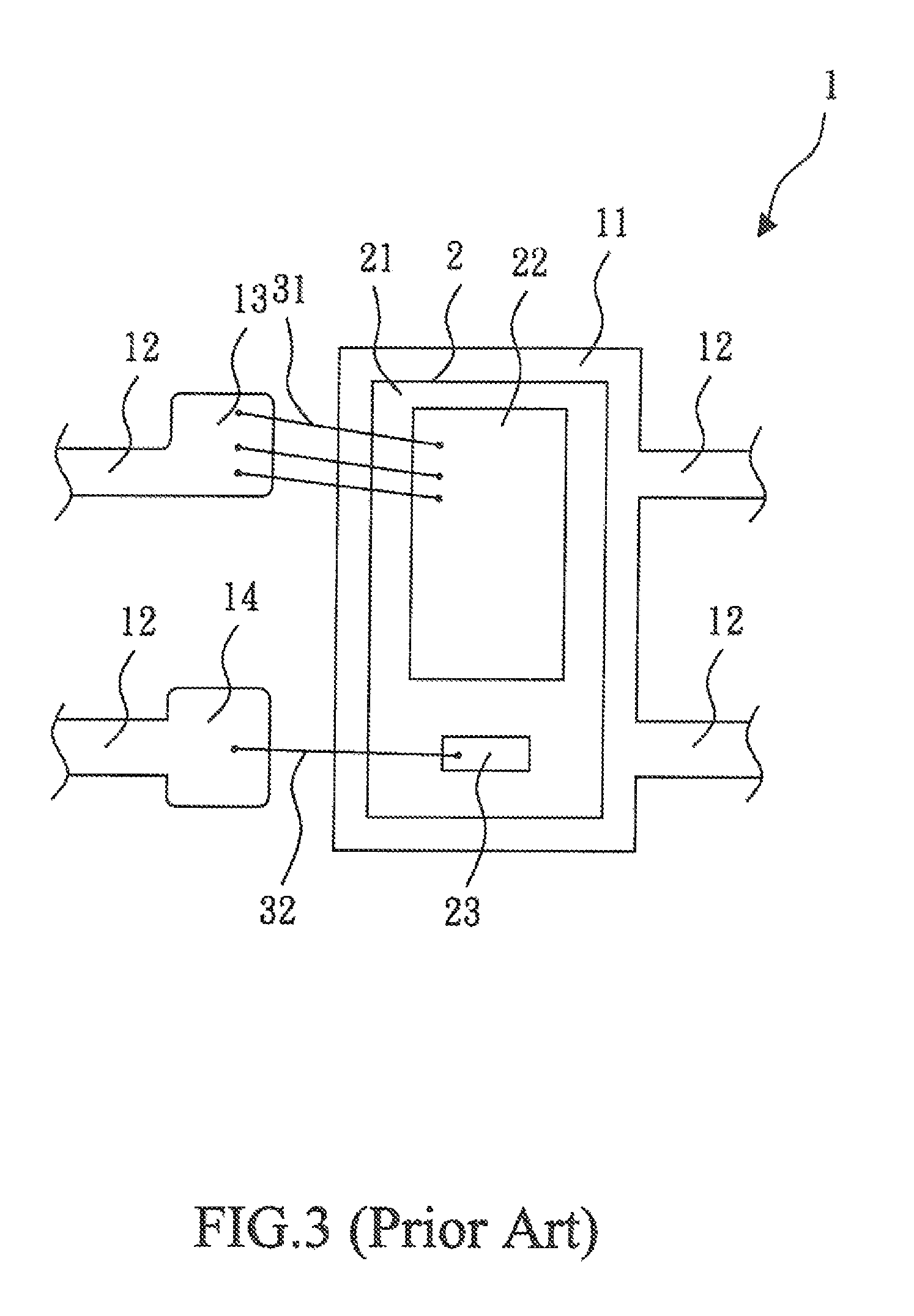
Referring now to FIG. 3, a wiring process is performed. A first wire 31 is used to connect the source pin 13 of the lead frame 1 and the source conductive region 22 of the chip 2, and a second wire 32 is used to connect the gate pin 14 of the lead frame 1 and the gate conductive region 23 of the chip 2. The method may then continue with a molding process and a cutting process to further form the semiconductor package.
The conventional method for making the semiconductor package has the following disadvantages. The first wire 31 and the second wire 32 are gold wires, so the material cost is high. Moreover, during the wire bonding process, a wiring machine is used to form the first wire 31 and the second wire 32 one by one, which is time consuming. Further, a certain space must be reserved between the first wire 31 and the second wire 32 for the movement of a wiring head of the wiring machine, so that the space between the first wire 31 and the second wire 32 cannot be effectively narrowed. If the size of the chip 2 is reduced to a certain degree, the conventional method is not applicable.
Therefore, there is a continuing need to provide an improved semiconductor package and a method for making the same, to solve the above problems.
SUMMARY OF THE INVENTION
The present technology may best be understood by referring to the following description and accompanying drawings that are used to illustrate embodiments of the present technology directed toward a semiconductor package and method for making the same. The techniques, in one or more embodiments, include a semiconductor package of a transistor without any wires and a method of making the same.
In one embodiment a method of fabricating a semiconductor package includes providing a substrate lead frame, wherein the substrate lead frame comprises a substrate frame, at least one first substrate lead, at least one second substrate lead, and at least one third substrate lead, wherein the first substrate lead is connected to the substrate frame, the second substrate lead and the third substrate lead face a side of the first substrate lead, and wherein the second substrate lead has a first extension portion connected to the substrate frame, and the third substrate lead has a second extension portion connected to the substrate frame. At least one IC chip is also provided, wherein the at least one IC chip has an upper surface and a lower surface, the upper surface has a second conductive region and a third conductive region, and the lower surface has a first conductive region. The at least one IC chip is disposed on the substrate frame, wherein the first conductive region is electrically connected to the at least one first substrate lead. A clip lead frame is also provided, wherein the clip lead frame comprises a clip frame, at least one first clip lead, and at least one second clip lead, wherein the at least one first clip lead is connected to the clip frame and the at least one second clip is connected to the clip frame. The clip lead frame is disposed on the at least one IC chip, wherein the first clip lead is electrically connected to the second conductive region of the at least one IC chip, the second clip lead is electrically connected to the third conductive region of the at least one IC chip. A molding process is performed and then a cutting process is performed to remove to form at least one semiconductor package each including at least one IC chip.
In another embodiment, a semiconductor package includes a substrate lead frame, at least one chip, a clip lead frame and molding compound. The substrate lead frame includes at least one substrate frame, at least one first substrate lead, at least one second substrate lead, and at least one third substrate lead, wherein the first substrate lead is connected to the substrate frame, the second substrate lead and the third substrate lead face a side of the first substrate lead, the second substrate lead has a first extension portion, and the third substrate lead has a second extension portion. The at least one chip are each located on the respective first substrate lead and having an upper surface and a lower surface, wherein the upper surface has a second conductive region and a third conductive region, the lower surface has a first conductive region, and the first conductive region is electrically connected to the first substrate lead. The clip lead frame is located on the at least one chip and having at least one first clip lead and at least one second clip lead, wherein the first clip lead is electrically connected to the second conductive region of the at least one chip and the second substrate lead respectively, and the second clip lead is electrically connected to the third conductive region of the at least one chip and the third substrate lead respectively. The molding compound encapsulates the substrate lead frame, the at least one chip, and the clip lead frame, wherein the at least one first substrate lead, the at least one second substrate lead, the at least one third substrate lead are exposed to a side surface of the molding compound.
In yet another embodiment, a method of making a semiconductor package includes receiving a substrate lead frame including a plurality of substrate lead set portions and a substrate frame portion, wherein each substrate lead set includes a first substrate lead, a second substrate lead and a third substrate lead, and wherein each of the first substrate leads, second substrate leads and third substrate leads are coupled to the substrate frame portion by one or more substrate extensions. A plurality of IC chips are also received, wherein each IC chip includes a first conductive region on a first surface, and a second conductive region and a third conductive region on a second surface. Each of the plurality of IC chips are disposed on the first substrate lead. A clip lead frame is also received, the clip lead frame includes a plurality of clip lead set portions and a dip frame portion, wherein each clip lead set includes a first clip lead and a second clip lead, and wherein each of the first clip leads and second clip leads are coupled to the clip frame portion by one or more clip extensions. The clip lead frame is disposed on the plurality of IC chips, wherein each of the first clip leads is disposed between the second conductive region on a respective IC chip and the respective second substrate lead of the substrate lead frame and each of the second clip leads is disposed between the third conductive region on a respective IC chip and the respective third substrate lead of the substrate lead frame. The first substrate lead is coupled to the first conductive region of the respective IC chip. The first clip lead is coupled between the second conductive region on the respective IC chip and the second substrate lead. The second clip lead is coupled between the third conductive region on the respective IC chip and the third substrate lead for each of the plurality of IC chips. The substrate lead frame, the plurality of IC chips and the clip lead frame are then encapsulated before cutting the lead frame, plurality of IC chips and clip lead frame in a plurality of predetermined locations to separate the first substrate leads, second substrate leads and third substrate leads from the substrate frame and the first clip leads and the second clip leads from the clip frame to form packages each including at least one IC chip including the first substrate lead coupled to the respective IC chip, the first clip lead coupled between the respective IC chip and second substrate lead, and second clip lead coupled between the respective IC chip and the third substrate lead.
This Summary is provided to introduce a selection of concepts in a simplified form that are further described below in the Detailed Description. This Summary is not intended to identify key features or essential features of the claimed subject matter, nor is it intended to be used to limit the scope of the claimed subject matter.
BRIEF DESCRIPTION OF THE DRAWINGS
Embodiments of the present technology are illustrated by way of example and not by way of limitation, in the figures of the accompanying drawings and in which like reference numerals refer to similar elements and in which:
FIGS. 1, 2 and 3 show a schematic view illustrating various stages of a method for making a semiconductor package, according to the conventional art.
FIGS. 4 through 23 show a schematic view illustrating various stages of a method for making a semiconductor package, in accordance with one embodiment of the present technology.
DETAILED DESCRIPTION
Reference will now be made in detail to the embodiments of the present technology, examples of which are illustrated in the accompanying drawings. While the present technology will be described in conjunction with these embodiments, it will be understood that they are not intended to limit the invention to these embodiments. On the contrary, the invention is intended to cover alternatives, modifications and equivalents, which may be included within the scope of the invention as defined by the appended claims. Furthermore, in the following detailed description of the present technology, numerous specific details are set forth in order to provide a thorough understanding of the present technology. However, it is understood that the present technology may be practiced without these specific details. In other instances, well-known methods, procedures, components, and circuits have not been described in detail as not to unnecessarily obscure aspects of the present technology.
In this application, the use of the disjunctive is intended to include the conjunctive. The use of definite or indefinite articles is not intended to indicate cardinality. In particular, a reference to "the" object or "a" object is intended to denote also one of a possible plurality of such objects. It is also to be understood that the phraseology and terminology used herein is for the purpose of description and should not be regarded as limiting.
Embodiments of the present technology are directed toward semiconductor packaging techniques. Referring now to FIG. 4, a stage in the manufacture of a semiconductor package, in accordance with one embodiment of the present technology, is shown. The stage illustrated in FIG. 4 will be further explained with reference to FIG. 5, which is a partially enlarged view of FIG. 4. FIGS. 4 and 5 illustrate a substrate lead frame 400 including a frame portion 405 and a plurality of lead set 410, 420, 430 portions. For each set of leads, a first substrate lead 410 is coupled to the frame portion 405 by one or more extensions 415. A second substrate lead 420 and a third substrate lead 430 are coupled to the frame portion 405 by one or more respective extensions 425, 435. The second substrate lead 420 and third substrate lead 430 are separated by a space from the first substrate lead 410 along a first side 411 of the first substrate lead 410. In one implementation, the first substrate lead 410 is a first drain interconnect, the second substrate lead 420 is a first source interconnect, and the third substrate lead 430 is a first gate interconnect. In another implementation, the first substrate lead 410 is a first source interconnect, the second substrate lead 420 is a first drain interconnect, and the third substrate lead 430 is a first gate interconnect.
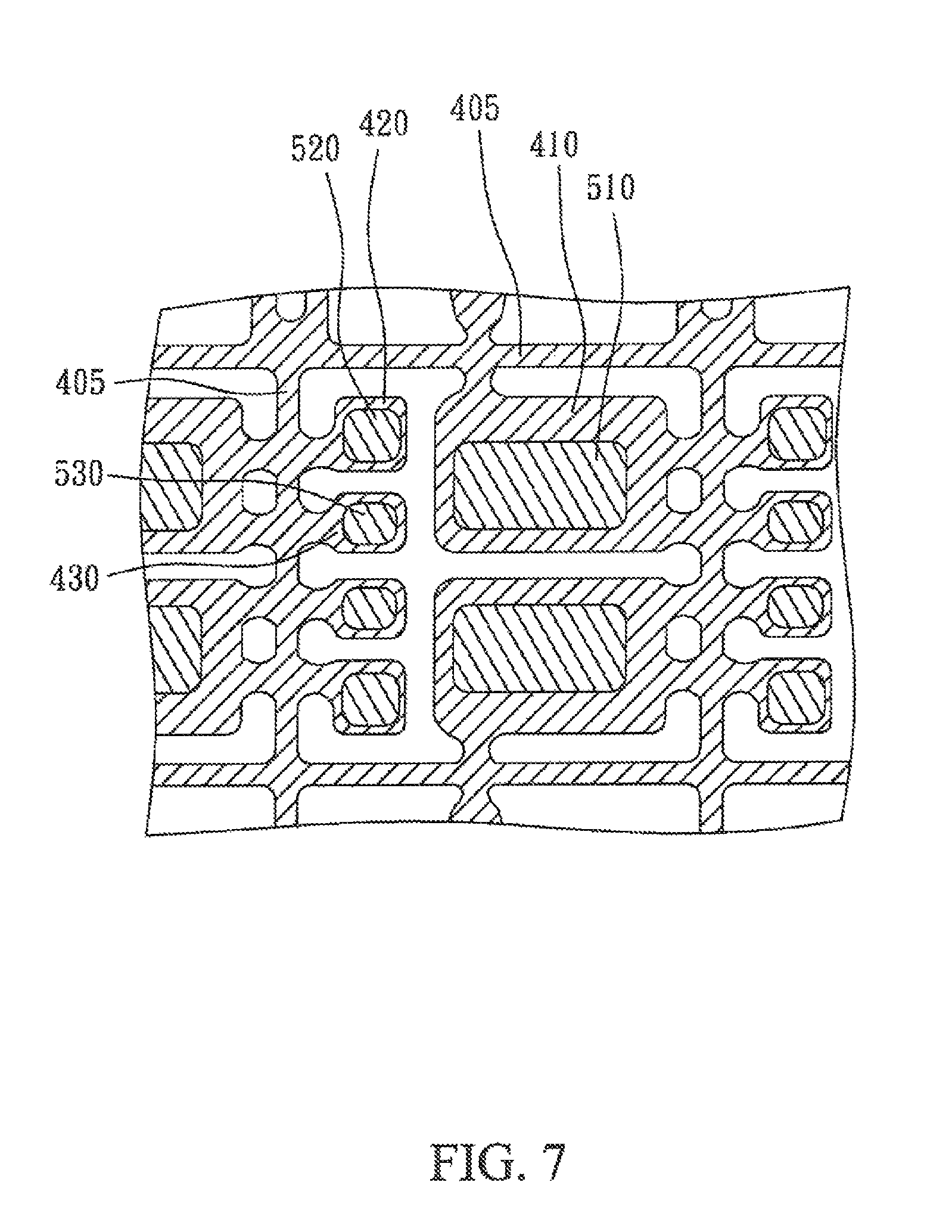
Referring now to FIG. 6, another stage in the manufacture of a semiconductor package, in accordance with one embodiment of the present technology, is shown. The stage illustrated in FIG. 6 will be further explained with reference to FIG. 7, which is a partially enlarged view of FIG. 6. A first solder 510 is formed on the first substrate lead 410, a second solder 520 is formed on the second substrate lead 420, and a third solder 530 is formed on the third substrate lead 430.
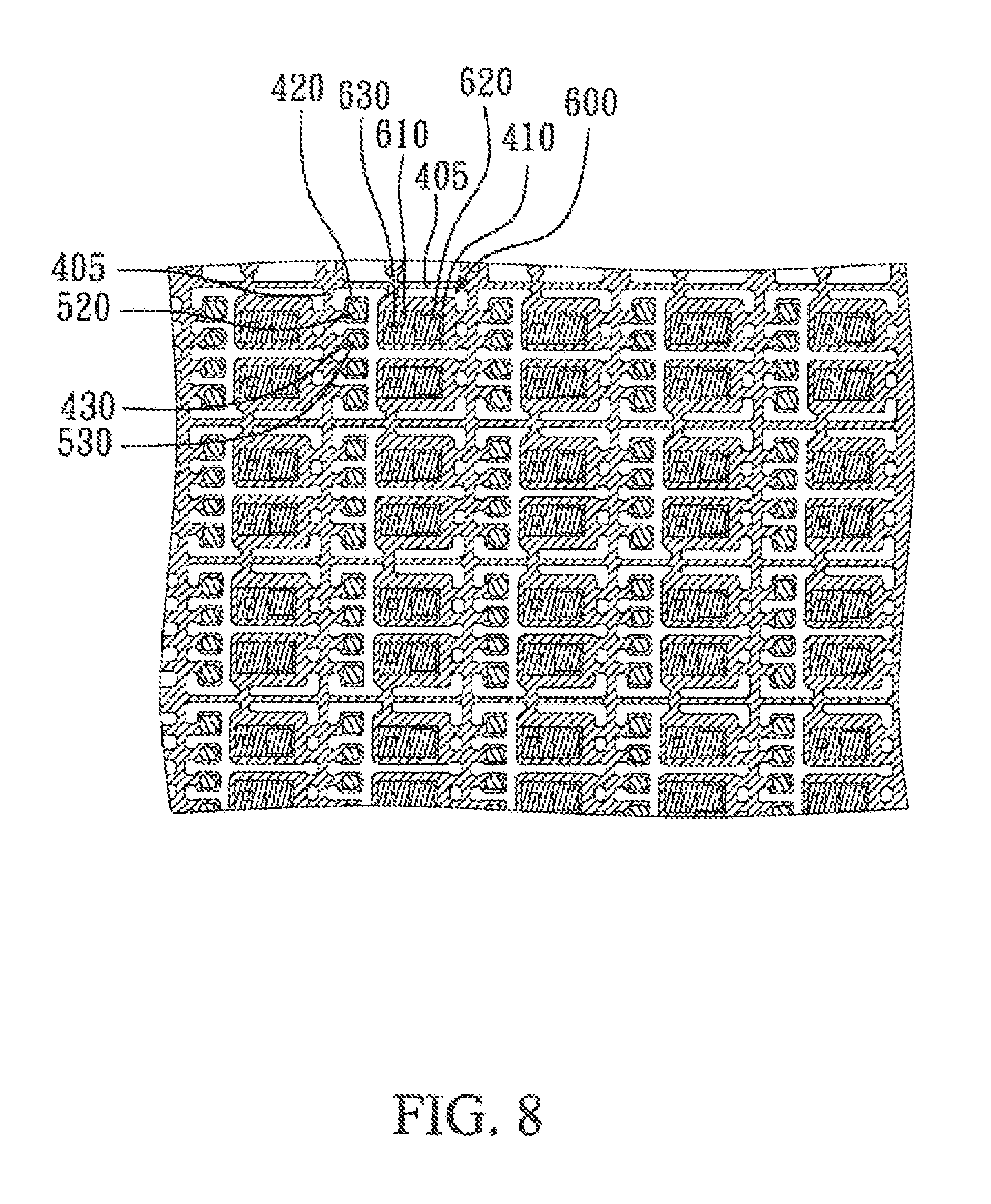
Referring now to FIG. 8, yet another stage in the manufacture of a semiconductor package, in accordance with one embodiment of the present technology, is shown. The stage illustrated in FIG. 8 will be further explained with reference to FIG. 9, which is a partially enlarged view of FIG. 8. An integrated circuit (IC) chip 600 is disposed on the first substrate lead 410 of each set of leads of the substrate lead frame. In one implementation, the IC chip 600 is a power metal-oxide-semiconductor field-effect transistor (MOSFET). Each IC chip 600 has an upper surface 610 and a lower surface 640 (not shown in FIGS. 8 and 9). The lower surface has a first conductive region (not shown in FIGS. 8 and 9) disposed on the second solder 520 on the first substrate lead 410 of the substrate lead frame 400. The upper surface 610 of the IC chip 600 has a second conductive region 620 and a third conductive region 630. In the one implementation, the first conductive region is a drain conductive region, the second conductive region 620 is a source conductive region, and the third conductive region 630 is a gate conductive region. In the other implementation, the first conductive region is a source conductiveregion, the second conductive region 620 is a drain conductive region, and the third conductive region 630 is a gate conductive region.
Referring now to FIG. 10, yet another stage in the manufacture of a semiconductor package, in accordance with one embodiment of the present technology, is shown. The stage illustrated in FIG. 10 will be further explained with reference to FIG. 11, which is a partially enlarged view of FIG. 10. As illustrated in FIGS. 10 and 11, a fourth solder 540 is formed on the second conductive region 620 and a fifth solder 550 is formed on the third conductive region 630 of the IC chip 600.
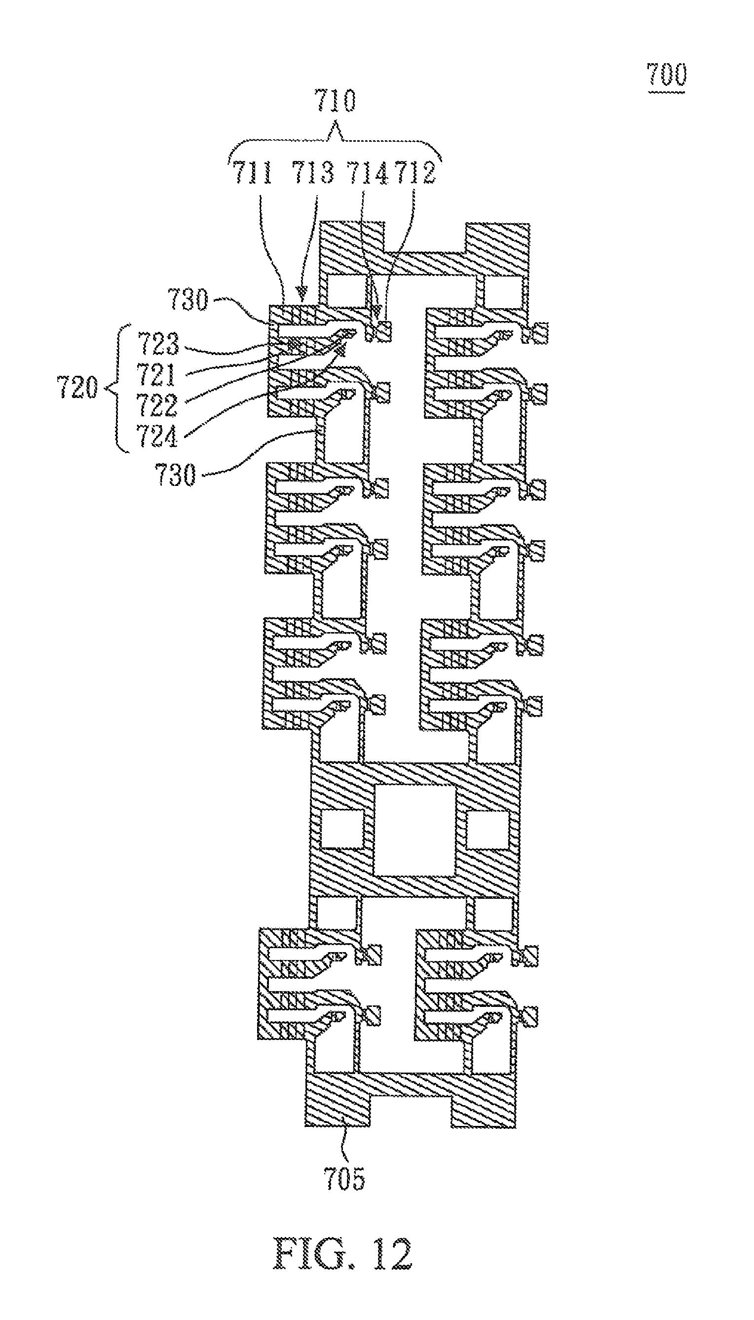
Referring now to FIG. 12, yet another stage in the manufacture of a semiconductor package, in accordance with one embodiment of the present technology, is shown. The stage illustrated in FIG. 12 will be further explained with reference to FIGS. 13, 14 and 15. FIG. 13 is a partially enlarged view of FIG. 12. FIG. 14 is a cross-sectional view of FIG. 12 taken along line 14-14, and FIG. 15 is a cross-section view of FIG. 12 taken along line 15-15. FIGS. 12-15 illustrate a clip lead frame 700 including a frame portion 705 and a plurality of lead set 710, 720 portions. Each set of clip leads 710, 720 are coupled to the frame portion 705 by one or more respective extensions 730. In one implementation, the frame portion 705 includes one or more larger physical areas for providing an area required by absorption. In the one implementation, a first clip lead 710 is a second source interconnect, and a second clip lead 720 is a second gate interconnect. In the other implementation, the first clip lead 710 is a second drain interconnect, and the second clip lead 720 is a second gate interconnect.
Each of the first clip leads 710 includes a first end 711, a second end 712, a first recess 713 and a second recess 714. Each of the second clip leads 720 includes a first end 721, a second end 722, a first recess 723, and a second recess 724.
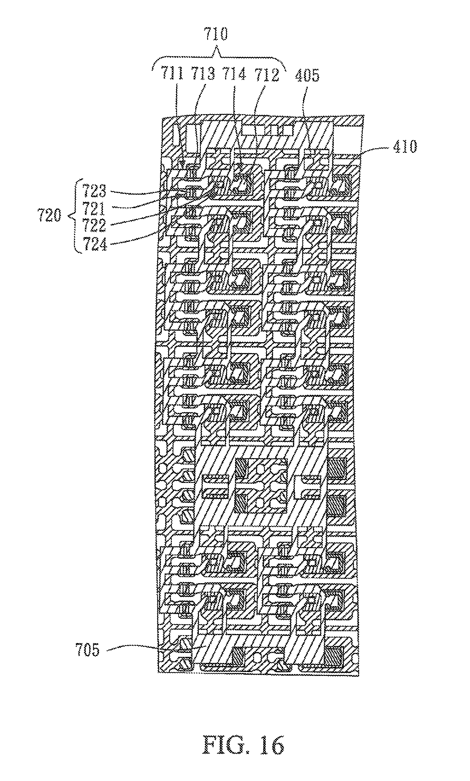
Referring now to FIG. 16, yet another stage in the manufacture of a semiconductor package, in accordance with one embodiment of the present technology, is shown. The stage illustrated in FIG. 16 will be further explained with reference to FIGS. 17 and 18. FIG. 17 is a partially enlarged view of FIG. 16. FIG. 18 is a cross-sectional view of FIG. 16 taken along line 18-18. FIGS. 16-18 illustrate assembly of the substrate lead frame 400, the IC chips 600, and the clip lead frame 700. The first clip lead 710 is disposed at the first recess 712 on the second solder 520 on the second substrate lead 420, and the second end 712 of the first clip lead 710 is disposed on the fourth solder 540 on the second conductive region 620 of the IC chip 600. The second clip lead 720 is disposed at the first recess 724 on the third solder 530 on the third substrate lead 430, and the second end 722 of the second clip lead 720 is disposed on the fifth solder 550 on the third conductive region 630 of the IC chip 600.
A solder reflow process is performed to electrically and mechanically connect the clip leads 710, 720 of the clip lead frame 700, the IC chips 600 and the substrate leads 410, 420, 430 of the substrate lead frame 400 together. As a result, the first clip lead 710 is electrically and mechanically coupled at the first recess 712 to the second substrate lead 420, and the second end 712 of the first clip lead 710 is electrically and mechanically coupled to the second conductive region 620 of the IC chip 600. The second clip lead 720 at the first recess 724 is electrically and mechanically coupled to the third substrate lead 430, and the second end 722 of the second clip lead 720 is electrically and mechanically coupled to the third conductive region 630 of the IC chip 600.
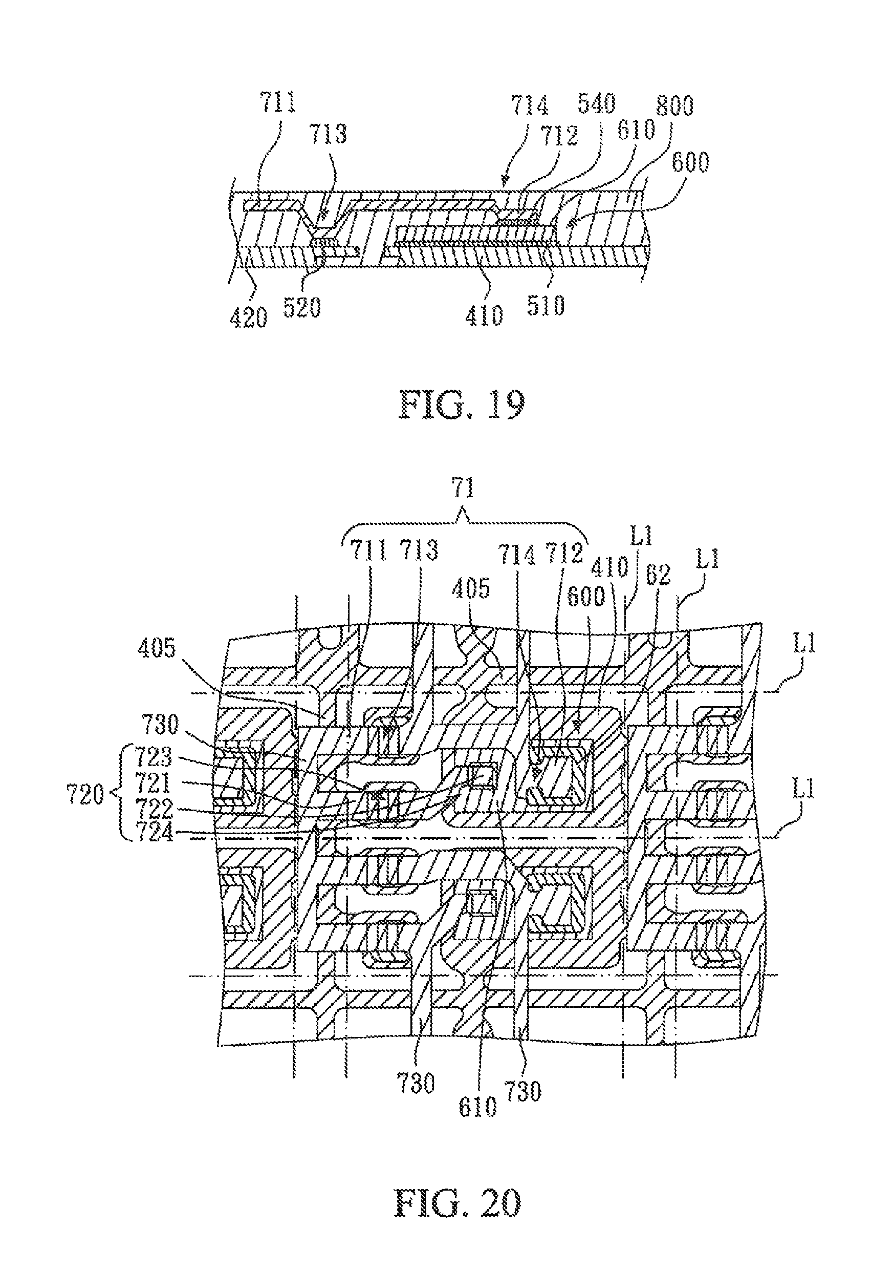
Referring now to FIG. 19, yet another stage in the manufacture of a semiconductor package, in accordance with one embodiment of the present technology, is shown. In FIG. 19 a molding process is performed. The substrate lead frame 400, the IC chips 600 and the clip lead frame 700 coupled together are placed in a mold cavity (riot shown), and then a molding compound 800 is filled in the mold cavity to encapsulate the substrate lead frame 400, the IC chips 600 and the clip lead frame 700. In one implementation, the first, second and third substrate leads 410, 420, 430 are exposed outside the molding compound 800.
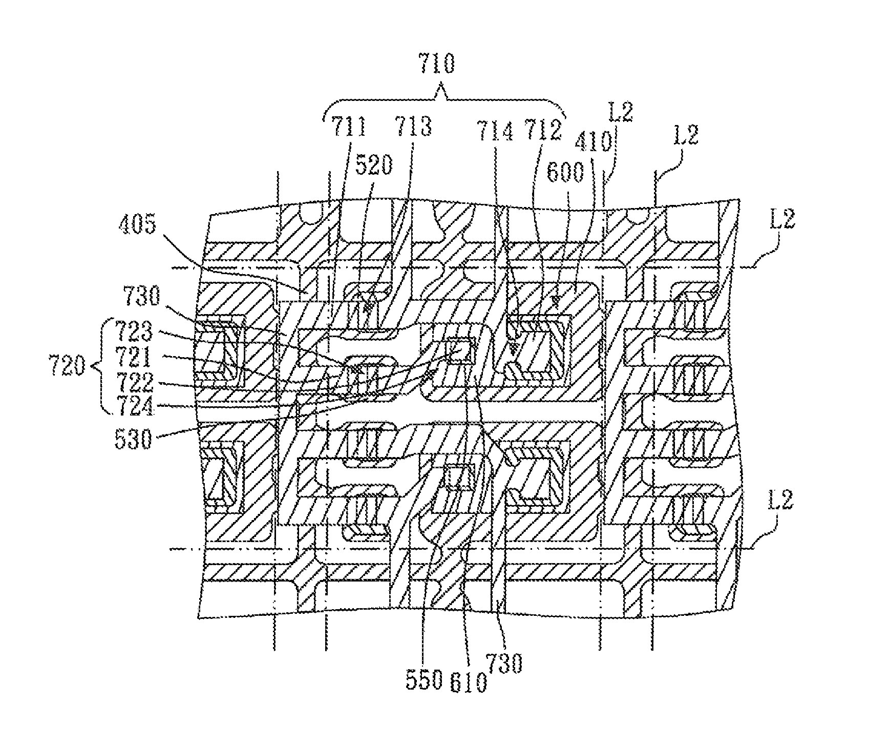
Referring now to FIGS. 20 and 21, yet another stage in the manufacture of a semiconductor package, in accordance with one embodiment of the present technology, is shown. As illustrated in FIG. 20, a cutting, process may be performed along first cutting lines L1. As illustrated in FIG. 21, an alternative cutting process may be performed along second cutting lines L2. Cutting along lines L1 or L2 separates the substrate leads 410, 420, 430 from the substrate frame 405 and from each other. Cutting along lines L1 or L2 also separates the clip leads 710, 720 from the clip frame 705 and from each other. However, the second substrate lead 420 remains electrically and mechanically coupled to the first clip lead 710 and the third substrate lead 430 remains electrically and mechanically coupled to the second clip lead 720.
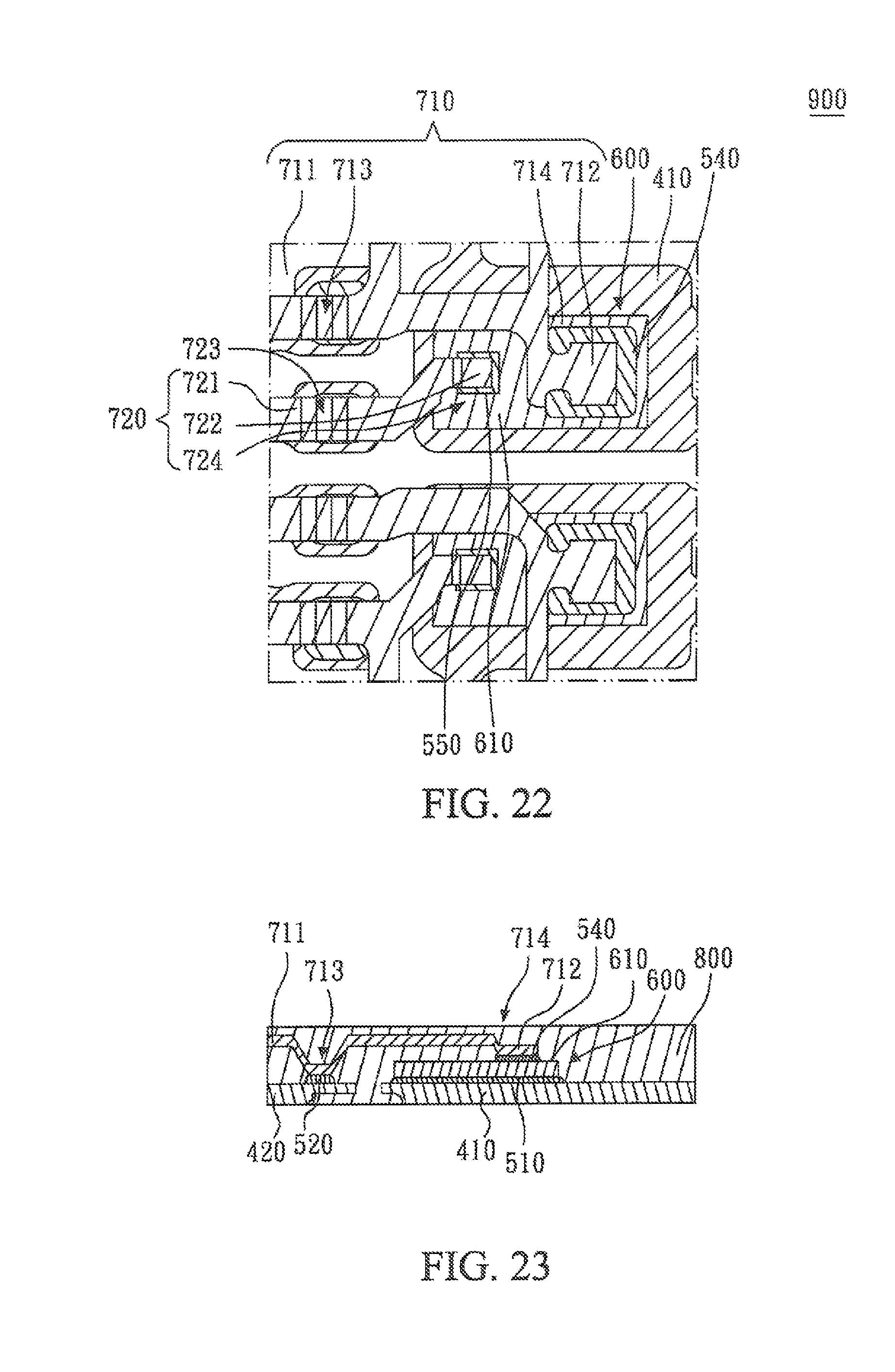
Referring now to FIGS. 22 and 23, yet another stage in the manufacture of a semiconductor package, in accordance with another embodiment of the present technology, is shown. FIG. 22 shows a top view of a semiconductor package 900 inside the molding compound. FIG. 23 shows a side sectional view of the semiconductor package 900. FIG. 22 illustrates the semiconductor package 900 including two IC chips 600 resulting from cutting along cut lines L2 in FIG. 21.
The semiconductor package 900, in accordance with embodiments of the present invention includes one or more IC chips 600. A first conductive region on a first surface of a respective IC chip 600 is electrically and mechanically coupled to a first substrate lead 410. A first clip lead 710 is electrically and mechanically coupled between a second conductive region on the second surface of the respective IC chip 600 and a second substrate lead 420. A second clip lead 720 is electrically and mechanically coupled between a third conductive region on the second surface of the respective IC chip 600 and a third substrate lead 420. The one or more IC chips 600, the respective first, second and third substrate leads 410, 420, 430 and the first and second clip leads 710, 720 are encapsulated, except for package contact portions of the first, second and third substrate leads 410, 420, 430. In the one implementation, the first substrate lead 410 is a drain interconnect, the coupled together first clip lead 710 and second substrate lead 420 is a source interconnect, and the coupled together second clip lead 720 and third substrate lead 430 is a gate interconnect of the respective IC chip 600 within the package 900. In the other implementation, the first substrate lead 410 is a source interconnect, the coupled together first clip lead 710 and second substrate lead 420 is a drain interconnect, and the coupled together second clip lead 720 and third substrate lead 430 is a gate interconnect of the respective IC chip 600 within the package 900.
Embodiments of the present technology are advantageously adaptable to manufacturing integrated circuit packages including one or more IC chips. Moreover, embodiments of the present technology do not utilize gold wires to may package interconnects, which effectively saves on material cost. In addition, the whole clip lead frame 700 of the present technology is integrally placed to effectively save processing time. The clip lead frame 700 may be fabricated through etching or other sophisticated techniques to narrow a space between the clip leads 710, 720, so that the clip lead frame 700 is applicable to IC chips 600 having a small size.
The foregoing descriptions of specific embodiments of the present technology have been presented for purposes of illustration and description. They are not intended to be exhaustive or to limit the invention to the precise forms disclosed, and obviously many modifications and variations are possible in light of the above teaching. The embodiments were chosen and described in order to best explain the principles of the present technology and its practical application to thereby enable others skilled in the art to best utilize the present technology and various embodiments with various modifications as are suited to the particular use contemplated. It is intended that the scope of the invention be defined by the claims appended hereto and their equivalents.
* * * * *
D00000
D00001
D00002
D00003
D00004
D00005
D00006
D00007
D00008
D00009
D00010
D00011
D00012
D00013

D00014
D00015

D00016
D00017

D00018
XML
uspto.report is an independent third-party trademark research tool that is not affiliated, endorsed, or sponsored by the United States Patent and Trademark Office (USPTO) or any other governmental organization. The information provided by uspto.report is based on publicly available data at the time of writing and is intended for informational purposes only.
While we strive to provide accurate and up-to-date information, we do not guarantee the accuracy, completeness, reliability, or suitability of the information displayed on this site. The use of this site is at your own risk. Any reliance you place on such information is therefore strictly at your own risk.
All official trademark data, including owner information, should be verified by visiting the official USPTO website at www.uspto.gov. This site is not intended to replace professional legal advice and should not be used as a substitute for consulting with a legal professional who is knowledgeable about trademark law.