Die Support Structures And Related Methods
A1
U.S. patent application number 16/861740 was filed with the patent office on 2020-08-13 for die support structures and related methods. This patent application is currently assigned to SEMICONDUCTOR COMPONENTS INDUSTRIES, LLC. The applicant listed for this patent is SEMICONDUCTOR COMPONENTS INDUSTRIES, LLC. Invention is credited to Francis J. CARNEY, Chee Hiong CHEW, Eiji KUROSE, Yusheng LIN, Michael J. SEDDON, Soon Wei WANG.
| Application Number | 20200258750 16/861740 |
| Document ID | 20200258750 / US20200258750 |
| Family ID | 1000004786678 |
| Filed Date | 2020-08-13 |
| Patent Application | download [pdf] |


View All Diagrams
| United States Patent Application | 20200258750 |
| Kind Code | A1 |
| CARNEY; Francis J. ; et al. | August 13, 2020 |
DIE SUPPORT STRUCTURES AND RELATED METHODS
Abstract
Implementations of a semiconductor device may include a semiconductor die comprising a first largest planar surface, a second largest planar surface and a thickness between the first largest planar surface and the second largest planar surface, and a permanent die support structure coupled to one of the first largest planar surface, the second largest planar surface, the thickness, or any combination thereof. The thickness may be between 0.1 microns and 125 microns. The warpage of the semiconductor die may be less than 200 microns.
| Inventors: | CARNEY; Francis J.; (Mesa, AZ) ; SEDDON; Michael J.; (Gilbert, AZ) ; KUROSE; Eiji; (Oizumi-machi, JP) ; CHEW; Chee Hiong; (Seremban, MY) ; WANG; Soon Wei; (Seremban, MY) ; LIN; Yusheng; (Phoenix, AZ) | ||||||||||
| Applicant: |
|
||||||||||
|---|---|---|---|---|---|---|---|---|---|---|---|
| Assignee: | SEMICONDUCTOR COMPONENTS
INDUSTRIES, LLC Phoenix AZ |
||||||||||
| Family ID: | 1000004786678 | ||||||||||
| Appl. No.: | 16/861740 | ||||||||||
| Filed: | April 29, 2020 |
Related U.S. Patent Documents
| Application Number | Filing Date | Patent Number | ||
|---|---|---|---|---|
| 16702958 | Dec 4, 2019 | |||
| 16861740 | ||||
| 15679661 | Aug 17, 2017 | 10529576 | ||
| 16702958 | ||||
| 16395822 | Apr 26, 2019 | |||
| 15679661 | ||||
| 15679664 | Aug 17, 2017 | 10319639 | ||
| 16395822 | ||||
| Current U.S. Class: | 1/1 |
| Current CPC Class: | H01L 24/26 20130101; H01L 21/302 20130101; H01L 2224/94 20130101; H01L 24/04 20130101; H01L 23/12 20130101; H01L 21/565 20130101; H01L 23/3185 20130101; H01L 21/78 20130101; H01L 21/48 20130101; H01L 21/561 20130101 |
| International Class: | H01L 21/302 20060101 H01L021/302; H01L 21/56 20060101 H01L021/56; H01L 21/78 20060101 H01L021/78; H01L 23/00 20060101 H01L023/00; H01L 23/12 20060101 H01L023/12; H01L 21/48 20060101 H01L021/48; H01L 23/31 20060101 H01L023/31 |
Claims
1. A semiconductor device comprising: a semiconductor die comprising a first largest planar surface, a second largest planar surface and a thickness between the first largest planar surface and the second largest planar surface; and a permanent die support structure coupled to one of the first largest planar surface, the second largest planar surface, the thickness, or any combination thereof; wherein the thickness is between 0.1 microns and 125 microns; and wherein a warpage of the semiconductor die is less than 200 microns.
2. The device of claim 1, wherein the warpage of the semiconductor die is less than 25 microns.
3. The device of claim 1, wherein a perimeter of the semiconductor die is rectangular and a size of the semiconductor die is at least 6 mm by 6 mm.
4. The device of claim 1, wherein a perimeter of the semiconductor die is rectangular and a size of the semiconductor die is 211 mm by 211 mm or smaller.
5. The device of claim 1, wherein the permanent die support structure comprises a mold compound.
6. The device of claim 1, wherein a perimeter of the semiconductor die comprises a closed shape.
7. The device of claim 1, wherein the permanent die support structure comprises a perimeter comprising a closed shape.
8. The device of claim 1, further comprising a second permanent die support structure coupled to one of the first largest planar surface, the second largest planar surface, the thickness, or any combination thereof.
9. The device of claim 1, wherein the permanent die support structure comprises two or more layers.
10. A die support structure comprising: a material configured to be permanently coupled with a semiconductor die comprising a first largest planar surface, a second largest planar surface and a thickness between the first largest planar surface and the second largest planar surface; wherein the material is configured to be coupled to one of the first largest planar surface, the second largest planar surface, the thickness, or any combination thereof; and wherein the thickness of the semiconductor die is between 0.1 microns and 125 microns.
11. The die support structure of claim 10, wherein the material is configured to reduce a warpage of the semiconductor die to less than 200 microns.
12. The die support structure of claim 10, wherein the material is a mold compound.
13. The die support structure of claim 10, wherein the material is not a polyimide.
14. The die support structure of claim 10, wherein the material comprises a perimeter comprising a closed shape.
15. The die support structure of claim 10, wherein the material is a first portion of material and further comprising a second portion of material configured to be coupled to one of the first largest planar surface, the second largest planar surface, the thickness, or any combination thereof.
16. A method of forming a die support structure comprising: permanently coupling a material with a semiconductor die: wherein the semiconductor die comprises a first largest planar surface, a second largest planar surface and a thickness between the first largest planar surface and the second largest planar surface; and wherein the material is coupled with one of the first largest planar surface, the second largest planar surface, the thickness, or any combination thereof; and reducing a warpage of the semiconductor die to less than 200 microns through the material.
17. The method of claim 16, wherein the material is a mold compound.
18. The method of claim 16, wherein the material comprises a perimeter comprising a closed shape.
19. The method of claim 16, wherein the material is a first portion of material and further comprising: permanently coupling a second portion of material with one of the first largest planar surface, the second largest planar surface, the thickness, or any combination thereof.
20. The method of claim 19, wherein the second portion of material is a second layer of material coupled over the first portion of material.
Description
CROSS REFERENCE TO RELATED APPLICATIONS
[0001] This application is a continuation-in-part application of the earlier U.S. Utility patent application to Eiji Kurose entitled "Multi-Faced Molded Semiconductor Package and Related Methods," application Ser. No. 16/702,958, filed Dec. 4, 2019, now pending; which application is a divisional application of the earlier U.S. Utility patent application to Eiji Kurose entitled "Multi-Faced Molded Semiconductor Package and Related Methods," application Ser. No. 15/679,661, filed Aug. 17, 2017, now U.S. Pat. No. 10,529,576, issued Jan. 7, 2020, the disclosures of each which are hereby incorporated entirely herein by reference.
[0002] This application is also a continuation-in-part application of the earlier U.S. Utility patent application to Krishnan et al. entitled "Thin Semiconductor Package and Related Methods," application Ser. No. 16/395,822, filed Apr. 26, 2019, now pending; which application is a continuation of the earlier U.S. Utility patent application to Krishnan et al. entitled "Thin Semiconductor Package and Related Methods," application Ser. No. 15/679,664, filed Aug. 17, 2017, now U.S. Pat. No. 10,319,639, issued Jun. 11, 2019, the disclosures of each of which are hereby incorporated entirely herein by reference.
BACKGROUND
1. Technical Field
[0003] Aspects of this document relate generally to semiconductor packages, such as wafer scale or chip scale packages. More specific implementations involve packages including an encapsulating or mold compound.
2. Background
[0004] Semiconductor packages work to facilitate electrical and physical connections to an electrical die or electrical component in the package. A protective cover or molding has generally covered portions of the semiconductor packages to protect the electrical die or electrical component from, among other things, the environment, electrostatic discharge, and electrical surges.
SUMMARY
[0005] Implementations of a semiconductor device may include a semiconductor die comprising a first largest planar surface, a second largest planar surface and a thickness between the first largest planar surface and the second largest planar surface, and a permanent die support structure coupled to one of the first largest planar surface, the second largest planar surface, the thickness, or any combination thereof. The thickness may be between 0.1 microns and 125 microns. The warpage of the semiconductor die may be less than 200 microns.
[0006] Implementations of a semiconductor device may include one, all, or any of the following:
[0007] The warpage of the semiconductor die may be less than 25 microns.
[0008] The perimeter of the semiconductor die may be rectangular and a size of the semiconductor die may be at least 6 mm by 6 mm.
[0009] The perimeter of the semiconductor die may be rectangular and a size of the semiconductor die may be 211 mm by 211 mm or smaller.
[0010] The permanent die support structure may include a mold compound.
[0011] The perimeter of the semiconductor die may include a closed shape.
[0012] The permanent die support structure may include a perimeter comprising a closed shape.
[0013] The device may include a second permanent die support structure coupled to one of the first largest planar surface, the second largest planar surface, the thickness, or any combination thereof.
[0014] The permanent die support structure may include two or more layers.
[0015] Implementations of a die support structure may include a material configured to be permanently coupled with a semiconductor die comprising a first largest planar surface, a second largest planar surface and a thickness between the first largest planar surface and the second largest planar surface where the material may be configured to be coupled to one of the first largest planar surface, the second largest planar surface, the thickness, or any combination thereof. The thickness of the semiconductor die may be between 0.1 microns and 125 microns.
[0016] Implementations of a die support structure may include one, all, or any of the following:
[0017] The material may be configured to reduce a warpage of the semiconductor die to less than 200 microns.
[0018] The material may be a mold compound.
[0019] The material may not be a polyimide.
[0020] The material may include a perimeter comprising a closed shape.
[0021] The material may be a first portion of material and may include a second portion of material configured to be coupled to one of the first largest planar surface, the second largest planar surface, the thickness, or any combination thereof.
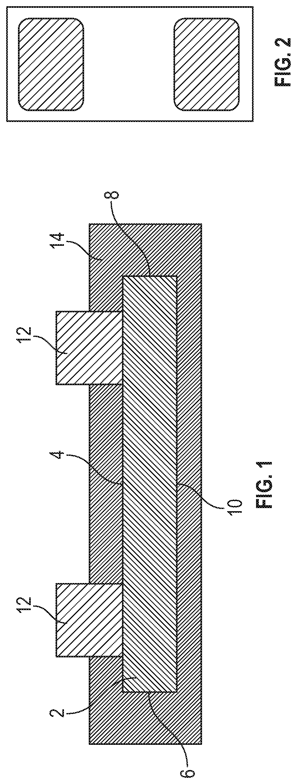
[0022] Implementations of a method of forming a die support structure may include permanently coupling a material with a semiconductor die. The semiconductor die may include a first largest planar surface, a second largest planar surface and a thickness between the first largest planar surface and the second largest planar surface, and the material may be coupled with one of the first largest planar surface, the second largest planar surface, the thickness, or any combination thereof. The method may include reducing a warpage of the semiconductor die to less than 200 microns through the material.
[0023] Implementations of a method of forming a die support structure may include one, all, or any of the following:
[0024] The material may be a mold compound.
[0025] The material may include a perimeter comprising a closed shape.
[0026] The material may be a first portion of material and may include: permanently coupling a second portion of material with one of the first largest planar surface, the second largest planar surface, the thickness, or any combination thereof.
[0027] The second portion of material may be a second layer of material coupled over the first portion of material.
[0028] The foregoing and other aspects, features, and advantages will be apparent to those artisans of ordinary skill in the art from the DESCRIPTION and DRAWINGS, and from the CLAIMS.
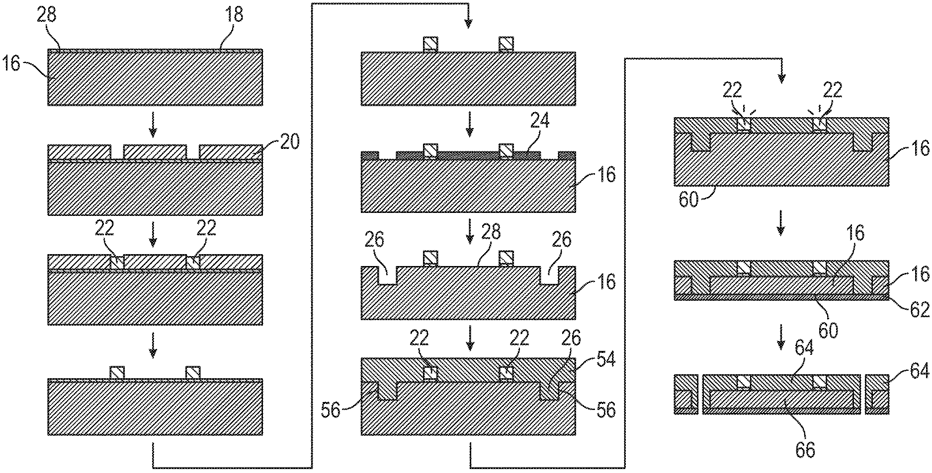
BRIEF DESCRIPTION OF THE DRAWINGS
[0029] Implementations will hereinafter be described in conjunction with the appended drawings, where like designations denote like elements, and:
[0030] FIG. 1 is a cross sectional side view of a semiconductor package;
[0031] FIG. 2 is a top view of a semiconductor package;
[0032] FIG. 3 is a first process flow illustrating the formation of a semiconductor package;
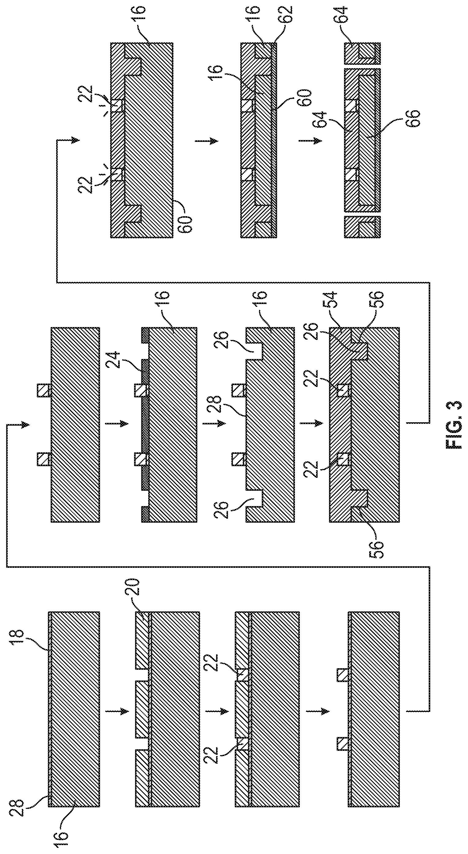
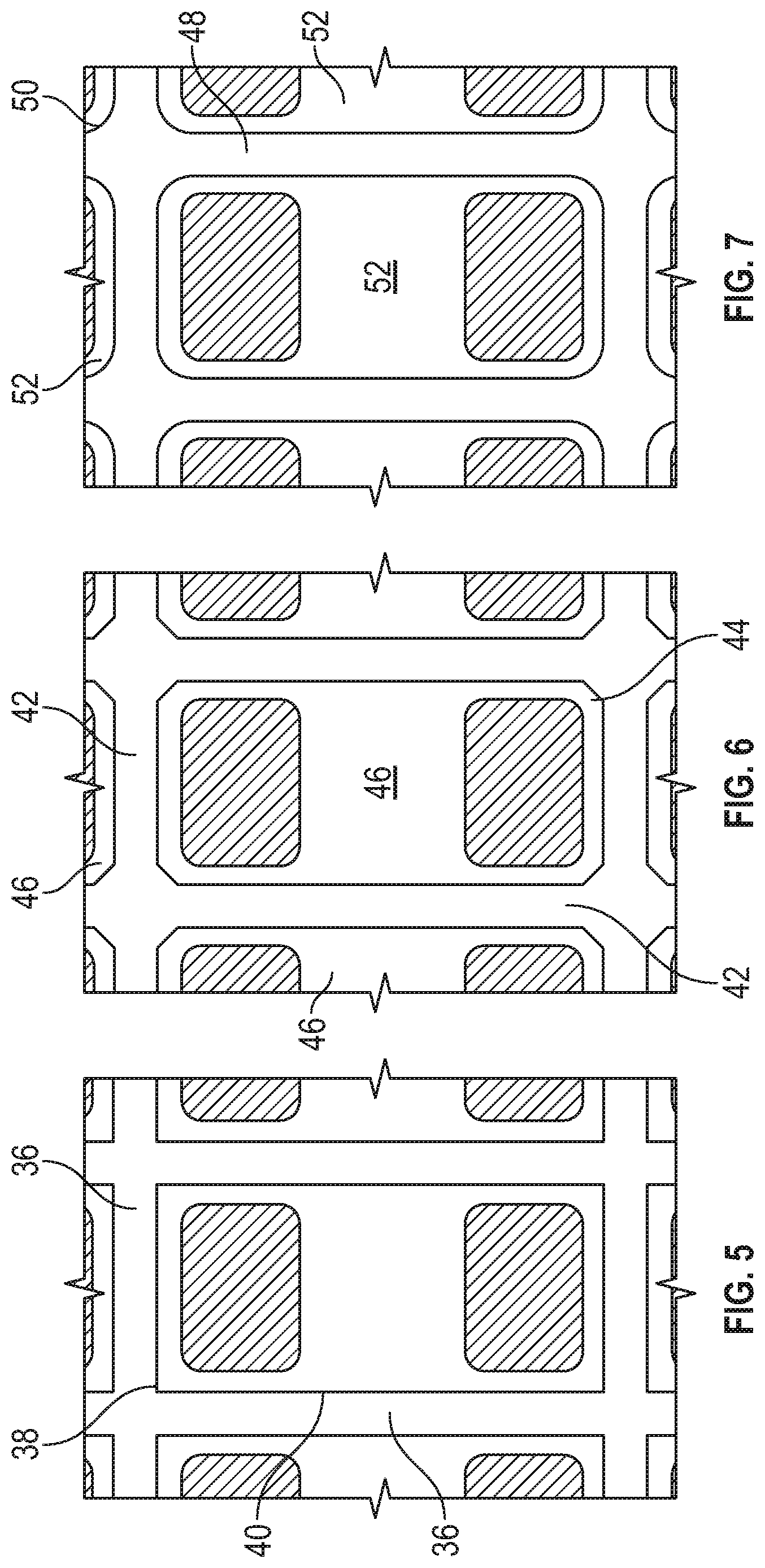
[0033] FIG. 4 is a top view of a semiconductor wafer with a plurality of notches cut therein;
[0034] FIG. 5 is a top view of a semiconductor wafer with a plurality of notches etched therein;
[0035] FIG. 6 is a top view of a second implementation of a semiconductor wafer with a plurality of notches etched therein;
[0036] FIG. 7 is a top view of a third implementations of a semiconductor wafer with a plurality of notches etched therein;
[0037] FIG. 8 is a cross sectional view of a portion of a wafer with molding applied thereto;
[0038] FIG. 8A is a magnified cross sectional view of the bond between a mold and a sidewall of a notch formed in the die;
[0039] FIG. 9 is a second process flow illustrating the formation of a semiconductor package;
[0040] FIG. 10 is a third process flow illustrating a portion of the formation of a semiconductor package.
[0041] FIG. 11 illustrates a first alternative for forming the notches in the third process flow.
[0042] FIG. 12 illustrates a second alternative for forming the notches in the third process flow;
[0043] FIG. 13 illustrates a third alternative for forming the notches in the third process flow;
[0044] FIG. 14 illustrates a fourth alternative for forming the notches in the third process flow;
[0045] FIG. 15 is a fourth process flow illustrating the formation of a semiconductor package;
[0046] FIG. 16 is an illustration of a process flow for forming an ultra-thin semiconductor package;
[0047] FIG. 17 is a cross sectional view of an ultra-thin semiconductor package formed by the process of FIG. 16;
[0048] FIG. 18 is a cross sectional view of an ultra-thin semiconductor package with a notch formed therein;
[0049] FIG. 19 is an illustration of a process flow for forming an ultra-thin semiconductor package with a portion of the die exposed;
[0050] FIG. 20 is a cross sectional view of an ultra-thin semiconductor package formed by the process of FIG. 19;
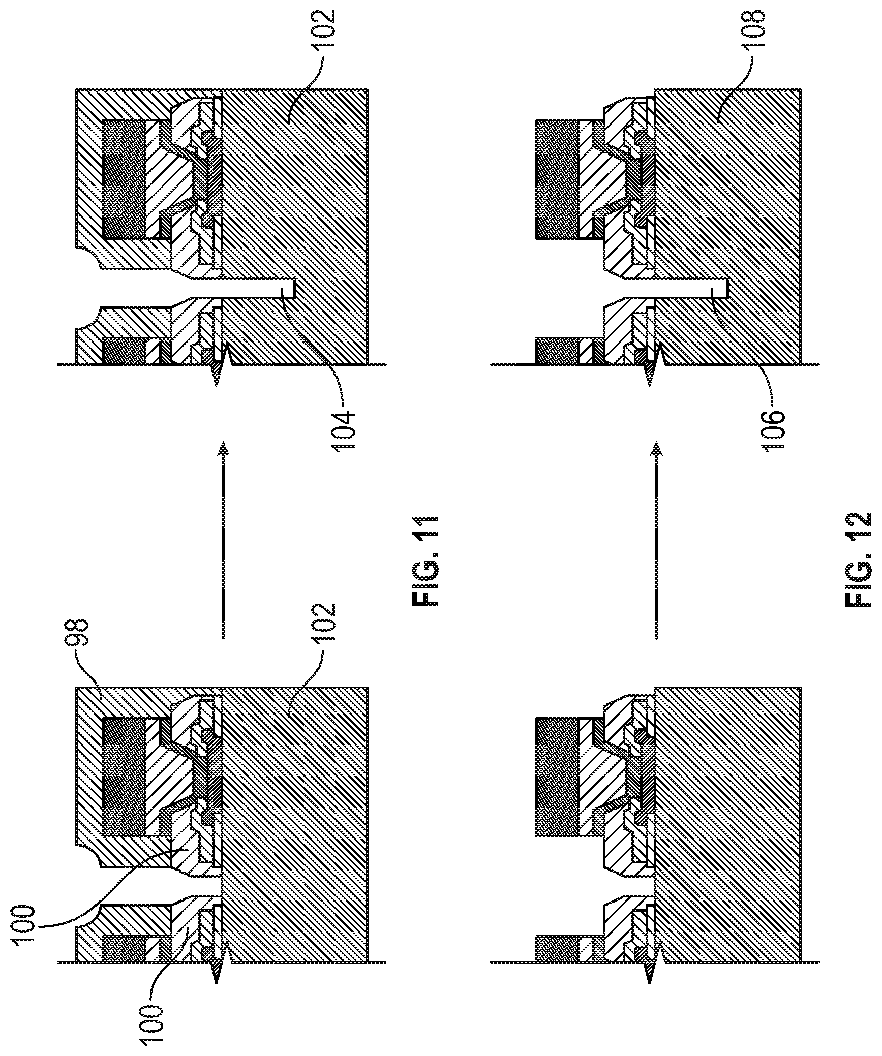
[0051] FIG. 21 is an illustration of a process flow for forming an ultra-thin semiconductor package with a notch formed therein;
[0052] FIG. 22 is a cross sectional view of an ultra-thin semiconductor package formed by the process of FIG. 21;
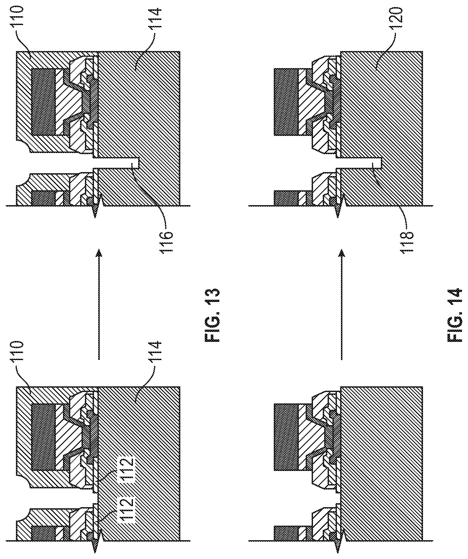
[0053] FIG. 23 is an illustration of a process flow for forming an ultra-thin semiconductor package with a portion of the die exposed;
[0054] FIG. 24 is a cross sectional view of an ultra-thin semiconductor package formed by the process of FIG. 23;
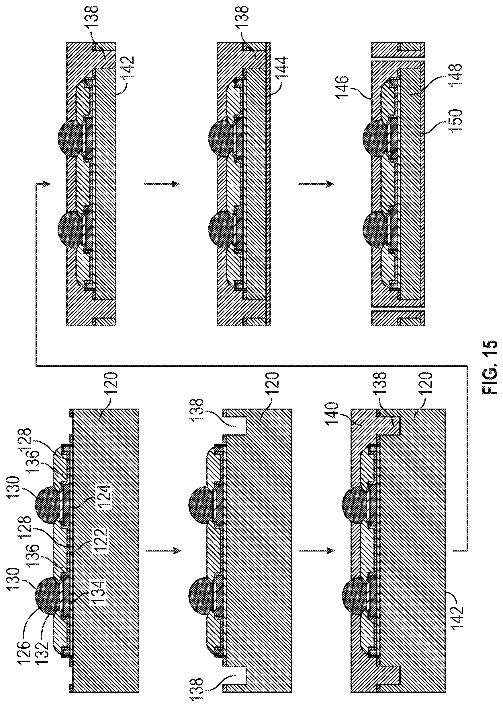
[0055] FIG. 25 is a perspective view of a first implementation of a permanent die support structure coupled with a thinned semiconductor die (die);
[0056] FIG. 26 is a perspective view of a second implementation of a permanent die support structure coupled with a thinned die;
[0057] FIG. 27 is a perspective view of a third implementation of a permanent die support structure coupled with a thinned die;
[0058] FIG. 28 is a perspective view of a fourth implementation of a permanent die support structure coupled with a thinned die;
[0059] FIG. 29 is a perspective view of a fifth implementation of a permanent die support structure coupled with a thinned die;
[0060] FIG. 30 is a perspective view of a sixth implementation of a permanent die support structure coupled with a thinned die;
[0061] FIG. 31 is a perspective view of a seventh implementation of a permanent die support structure coupled with a thinned die;
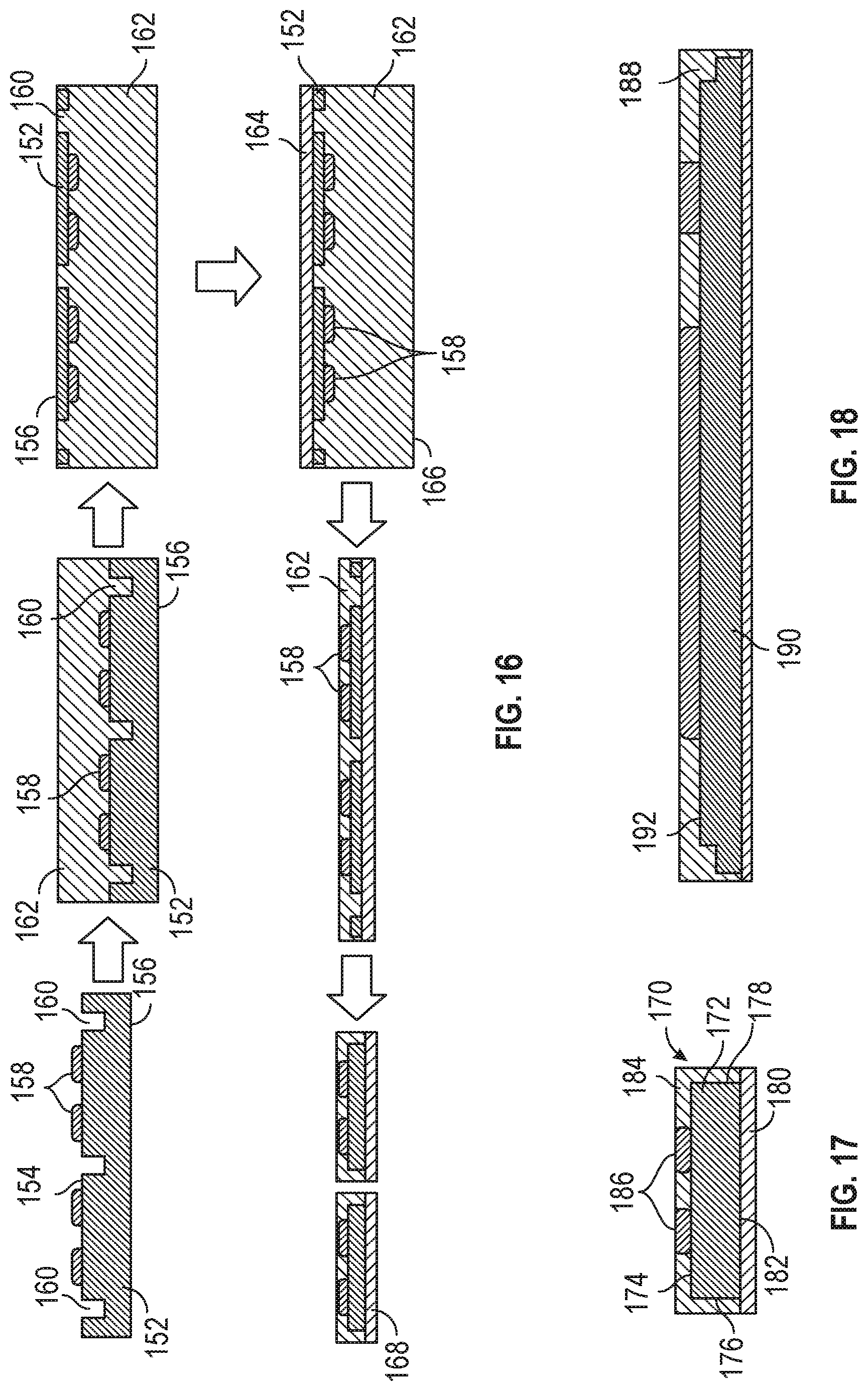
[0062] FIG. 32 is a perspective view of an eighth implementation of a permanent die support structure coupled with a thinned die;
[0063] FIG. 33 is a perspective view of an ninth implementation of a permanent die support structure coupled with a thinned die;
[0064] FIG. 34 is a perspective view of an tenth implementation of a permanent die support structure coupled with a thinned die;
[0065] FIG. 35 is a perspective view of an eleventh implementation of a permanent die support structure coupled with a thinned die;
[0066] FIG. 36 is a perspective view of an twelfth implementation of a permanent die support structure coupled with a thinned die;
[0067] FIG. 37 is a perspective view of a thirteenth implementation of a permanent die support structure coupled with a thinned die showing a first portion of material and a second portion of material;
[0068] FIG. 38 is a perspective view of a fourteenth implementation of a permanent die support structure coupled with a thinned die showing first, second, third, and fourth portions of material;
[0069] FIG. 39 is a perspective view of a fifteenth implementation of a permanent die support structure coupled with a thinned die;
[0070] FIG. 40 is a perspective view of a sixteenth implementation of a permanent die support structure coupled with a thinned die;
[0071] FIG. 41 is a perspective view of a seventeenth implementation of a permanent die support structure coupled with a thinned die showing first, second, third, and fourth portions of material;
[0072] FIG. 42 is a perspective view of an eighteenth implementation of a permanent die support structure coupled with a thinned die showing first, second, third, and fourth portions of material;
[0073] FIG. 43 is a perspective view of a nineteenth implementation of a permanent die support structure coupled with a thinned die showing a first portion of material and a second portion of material;
[0074] FIG. 44 is a perspective view of an twentieth implementation of a permanent die support structure coupled with a thinned die showing first, second, and third portions of material;
[0075] FIG. 45 is a side cross-sectional view of an implementation of a permanent die support structure coupled with a thinned die;
[0076] FIG. 46 is a side cross-sectional view of an implementation of a permanent die support structure coupled with a thinned die;
[0077] FIG. 47 is a side view of an implementation of a semiconductor substrate with a molded permanent die support structure coupled following partial singulation;
[0078] FIG. 48 is a top view of a semiconductor substrate with a plurality of permanent die support structures coupled over a plurality of die formed therein;
[0079] FIG. 49 is a top view of a die of the plurality of die of FIG. 48 showing the permanent die support structure with a varying thickness across the die support structure;
[0080] FIG. 50 is a side view of the die of FIG. 49 showing the thickness of the die and the permanent die support structure;
[0081] FIG. 51 is a side view of a semiconductor substrate with a plurality of saw streets formed thereon;
[0082] FIG. 52 is a side view of a full-thickness (original thickness) semiconductor substrate with a plurality of die with a corresponding plurality of permanent die support structures coupled thereto;
[0083] FIG. 53 is a side view of a thinned semiconductor substrate with a plurality of die with a corresponding plurality of permanent die support structures coupled thereto applied after thinning;
[0084] FIG. 54 is a side view of a thinned semiconductor substrate with a plurality of die with a corresponding plurality of permanent die support structures coupled thereto applied after formation of backmetal;
[0085] FIG. 55 is a side view of a partially thinned semiconductor substrate with a plurality of die with a corresponding plurality of permanent die support structures coupled thereto after a partial grind has been performed;
[0086] FIG. 56 is a side view of a thinned semiconductor substrate with a plurality of die with a corresponding plurality of permanent die support structures coupled thereto after a full grind has been performed but before or after a stress relief etching process is carried out.
DESCRIPTION
[0087] This disclosure, its aspects and implementations, are not limited to the specific components, assembly procedures or method elements disclosed herein. Many additional components, assembly procedures and/or method elements known in the art consistent with the intended die support structures and related methods will become apparent for use with particular implementations from this disclosure. Accordingly, for example, although particular implementations are disclosed, such implementations and implementing components may comprise any shape, size, style, type, model, version, measurement, concentration, material, quantity, method element, step, and/or the like as is known in the art for such die support structures, and implementing components and methods, consistent with the intended operation and methods.
[0088] Referring to FIG. 1, a cross sectional side view of a semiconductor package is illustrated. The semiconductor package includes a die 2 which includes a first side 4, a second side 6, a third side 8 opposite the second side 6, a fourth side, a fifth side opposite the fourth side (both fourth and fifth sides are located into and out of the drawing surface in this view), and a sixth side 10 opposite the first side 4. In various implementations, the second side 6 of the die 2, the third side 8 of the die, the fourth side of the die, and/or the fifth side of the die may include a notch therein.
[0089] In various implementations, one or more electrical contacts 12 are coupled to the first side 4 of the die 2. In various implementations, the electrical contacts are metal and may be, by non-limiting example, copper, silver, gold, nickel, titanium, aluminum, any combination or alloy thereof, or another metal. In still other implementations, the electrical contacts 12 may not be metallic but may rather be another electrically conductive material.
[0090] In various implementations, a first mold compound 14 covers the first, second, third, fourth, and fifth sides of the die. In various implementations, the mold compound may be, by non-limiting example, an epoxy mold compound, an acrylic molding compound, or another type of material capable of physically supporting the die and providing protection against ingress of contaminants. In various implementations, a laminate resin or second mold compound covers the sixth side 10 of the die.
[0091] The electrical contacts 12 each extend through a corresponding plurality of openings in the first mold compound 14. In various implementations, the electrical contacts 12 extend beyond the surface of the molding 14, as illustrated in FIG. 1, while in other implementations the electrical contacts are level or flush with the surface of the molding compound 14.
[0092] In various implementations, the sides of the die will have no chips or cracks, particularly on the semiconductor device side of the die. This is accomplished through forming the second, third, fourth, and fifth sides of each die using etching techniques rather than a conventional sawing technique. Such a method is more fully disclosed is association with the discussion of FIG. 3 herein.
[0093] Further, the first mold compound may be anchored to the second, third, fourth, and fifth sides of the die. In various implementations, the anchor effect is the result of interaction of the mold compound with a plurality of ridges formed along the second, third, fourth, and fifth sides of the die. This anchoring effect is more fully disclose in association with the discussion of FIG. 3 herein.
[0094] Referring to FIG. 2, a top view of a semiconductor package is illustrated. The molding compound 14 is clearly seen in FIG. 2 encompassing a perimeter of each electrical contact 12 (the shaded areas in FIG. 2) so that the entire first side of the die (along with every other side) is not exposed.
[0095] Referring to FIG. 3, a first process flow illustrating the formation of a semiconductor package is illustrated. In various implementations, the method for making a semiconductor package includes providing a wafer 16 which may include any particular type of substrate material, including, by non-limiting example, silicon, sapphire, ruby, gallium arsenide, glass, or any other semiconductor wafer substrate type. In various implementations, a metal layer 18 is formed on a first side 28 of the wafer 16 and may be formed using a sputtering technique. In other implementations, the metal layer 18 is formed using other techniques, such as, by non-limiting example, electroplating, electroless plating, chemical vapor deposition, and other methods of depositing a metal layer. In a particular implementation, the metal layer is a titanium/copper seed layer, while in other implementations, the metal layer may include, by non-limiting example, copper, titanium, gold, nickel, aluminum, silver, or any combination or alloy thereof.
[0096] In various implementations, a first photoresist layer 20 is formed and patterned over the metal layer 18. One or more electrical contacts 22 may be formed on the metal layer 18 and within the photoresist layer 20. In various implementations this may be done using various electroplating or electroless plating techniques, though deposition and etching techniques could be employed in various implementations. The electrical contacts 22 may be any type of electrical contact previously disclosed herein (bumps, studs, and so forth). In various implementations, the first photoresist layer 20 is removed through an ashing or solvent dissolution process and the metal layer 18 may be etched away after the electrical contacts are formed.
[0097] In various implementations, a second photoresist layer 24 is formed and patterned over the wafer 16. In various implementations, as illustrated in FIG. 3, the second patterned photoresist layer 24 does not cover the electrical contacts 22. In other implementations, the second photoresist layer is formed conformally over the electrical contacts along with the wafer. Referring to FIG. 9, a second process flow illustrating the formation of a semiconductor package is illustrated. In this process flow, a second photoresist layer 68 is formed as a conformal layer over the electrical contacts 70. Aside from this difference, the process depicted in FIG. 9 includes the same process steps as the process depicted in FIG. 3.
[0098] Referring back to FIG. 3, in various implementations, the method includes etching a plurality of notches 26 into the first side 28 of the wafer 16 using the second patterned photoresist layer. In various implementations, the width of the notches may be between about 50 and about 150 microns wide while in other implementations, the width of the notches may be less than about 50 microns or more than about 150 microns. In various implementations, the depth of the plurality of notches 26 may extend between about 25 and 200 microns into the wafer while in other implementations, the depth of the plurality of notches 26 may be less than about 25 microns or more than about 200 microns.
[0099] In various implementations, the plurality of notches may be formed using, by non-limiting example, plasma etching, deep-reactive ion etching, or wet chemical etching. In various implementations, a process marketed under the tradename BOSCH.RTM. by Robert Bosch GmbH, Stuttgart Germany (the "Bosch process"), may be used to form the plurality of notches 26 in the first side 28 of the wafer 16.
[0100] Referring now to FIG. 4, a top view of a conventional semiconductor wafer with a plurality of saw cuts surrounding the plurality of die is illustrated. Using a saw to cut notches in a semiconductor wafer invariably results in the production of chips and cracks on the device side of the die and in the sidewalls 34 of the notches 30. The presence of the cracks and chips has the potential to compromise the reliability of the semiconductor package if the cracks and chips propagate into the device portion of the semiconductor die. Since the saw process involves the rubbing of the rotating blade against the die surface, the chipping and cracking can only be managed through saw processing variables (wafer feed speed, blade kerf width, cut depth, multiple saw cuts, blade materials, etc.) but not eliminated. Furthermore, because the saw process relies on passing the wafer underneath the blades, only square and rectangular sized die are typically produced using conventional saw techniques.
[0101] Referring to FIG. 5, a top view of a semiconductor wafer with a plurality of notches etched therein is illustrated. In contrast to the appearance of the die processed using the conventional sawing method illustrated in FIG. 4, the plurality of notches 36 in the wafer 38 formed using etching techniques have edges and sidewalls 40 that do not exhibit cracks or chips therein. Because of the absence of the cracks and chips, the use of etching techniques to form a plurality of notches in a semiconductor wafer is likely to improve the reliability of the resulting semiconductor packages.
[0102] Furthermore, using etching techniques to form a plurality of notches in a wafer allows for different shapes of perimeters of die to be produced. In various implementations, the second photoresist layer described in relation to FIG. 3 may be patterned in a way to form a plurality of notches that do not form die with rectangular perimeters. For example, referring to FIG. 6, a top view of a second implementation of a semiconductor wafer with a plurality of notches etched therein is illustrated. In various implementations, a plurality of notches 42 may be formed in a wafer 44. The plurality of notches 42 may form eventual die 46 with perimeters that are octagons. Referring to FIG. 7, a top view of a third implementations of a semiconductor wafer with a plurality of notches etched therein is illustrated. In various implementations, a plurality of notches 48 may be formed in a wafer 50. The plurality of notches 48 may form eventual die 52 with perimeters that are rounded rectangles. In other implementations, a plurality of notches may be formed in a wafer that form eventual die with perimeters that are any other closed geometrical shape.
[0103] Referring back to FIG. 3, in various implementations, the plurality of notches 26 formed have two substantially parallel sidewalls that extend substantially straight into the first side 28 of the wafer 16. In other implementations, two or more stepwise notches are formed in the first side 28 of the wafer 16. Each stepwise notch may be formed by creating a first notch in the wafer, and then forming a second narrower notch within each first notch.
[0104] Referring to FIG. 3, an implementation of a method for forming a semiconductor package includes applying a first mold compound 54 into the plurality of notches 26 and over the first side of the wafer. In various implementations, as illustrated by FIG. 3, the first mold compound 54 may cover the electrical contacts 22. In other implementations, the first mold compound 54 may not completely cover the electrical contacts 22. The first mold compound may be applied using, by non-limiting example, a liquid dispensing technique, a transfer molding technique, a printer molding technique, or a compression molding technique. The molding compound may be an epoxy molding compound, an acrylic molding compound, or another type of molding compound disclosed herein.
[0105] In various implementations, the first mold compound 54 may be anchored to a plurality of sidewalls 56 of a plurality of notches 26. Referring now to FIG. 8, a cross sectional view of a portion of a wafer with molding applied thereto is illustrated. Referring now to FIG. 8A, a magnified cross sectional view of the bond between a mold and a sidewall of a notch formed in the die is illustrated. In various implementations, a plurality of ridges 58 may be formed in a sidewall 56 of each notch within the plurality of notches. In a particular implementation, the height of each ridge extending from the sidewall is substantially 0.2 microns tall with a pitch of substantially one micron. Thus, in implementations where the notch is 150 microns deep, there may be substantially 150 microns on each sidewall of the notch. In other implementations, the notches may be taller or shorter than 0.2 microns and may have a pitch more or less than one micron. The ridges may anchor the first mold compound 54 to the sidewalls 56 of the plurality of notches. In various implementations where the plurality of notches are etched using the Bosch process, the etching process may form ridges in the plurality of notches while etching the plurality of notches via the deposition/etching cycles of the deep reactive ion etch, thus increasing the adhesion between the first mold compound and the sidewall of each notch.
[0106] Referring back to FIG. 3, in various implementations where the first mold compound 54 covers the electrical contacts 22, the electrical contacts 22 may be exposed by grinding the first mold compound. In various implementations, a second side 60 of the wafer 16 may be ground to the plurality of notches 26 formed in the first side 28 of the wafer 16. In this way the various die of the semiconductor wafer are singulated from each other. In various implementations, the second side 60 of the wafer 16 may be ground using, by non-limiting example, a mechanical polishing technique, a chemical etching technique, a combination of a mechanical polishing and chemical etching technique, or any other grinding technique.
[0107] In various implementations, a second mold compound 62 or a laminate resin may be applied to the second side 60 of the wafer 16. In implementations where a second mold compound is applied, the mold compound may be any type of mold compound disclosed herein and may be applied using any technique disclosed herein.
[0108] In various implementations, as illustrated in the process flow depicted in FIG. 3, the first mold compound 54 is ground to expose the electrical contacts 22 before the second side 60 of the wafer 16 is ground and the second mold compound is applied. In other implementations, the first mold compound 54 may be ground to expose the electrical contacts 22 after the second side 60 of the wafer 16 is ground and the second mold compound is applied.
[0109] The method for making a semiconductor package includes singulating the wafer 16 into a plurality of semiconductor packages 64. The wafer 16 may be singulated by cutting or etching through the wafer where the plurality of notches 26 were originally formed. The wafer may be singulated by using, by non-limiting example, a saw, a laser, a waterjet, plasma etching, deep reactive-ion etching, or chemical etching. In various implementations, the Bosch process may be used to singulate the wafer 16. The method used to singulate the wafer may include singulating the wafer using thinner cuts or etches than were used to form the plurality of notches 26. In this manner, the first mold compound will cover the sides of each singulated die 66 within each semiconductor package 64. Specifically, in particular implementations the saw width used to singulate each semiconductor package may be between 20 and 40 microns thick. The semiconductor die within the semiconductor package may be covered by either a mold compound or a laminate resin on all six sides of the semiconductor die.
[0110] In various implementations, the first side of the die within each semiconductor package may include a perimeter that is, by non-limiting example, a rectangle, an octagon, a rectangle with rounded edges, or any other closed geometric shape.
[0111] Referring now to FIG. 10, a third process flow illustrating a portion of the formation of a semiconductor package is illustrated. In various implementations the method for forming a semiconductor package includes providing a wafer 72, which may be any type of wafer substrate disclosed herein. In various implementations, one or more metal pads 74 may be coupled to a first side 76 of the wafer 72. The metal pad may include, by non-limiting example, aluminum, copper, nickel silver, gold, titanium, or any combination or alloy thereof.
[0112] In various implementations, a first passivation layer 78 may be coupled to a portion of the first side 76 of the wafer 72. The first passivation layer 78 may be a silicon dioxide passivation layer in various implementations, though it could be any of a wide variety of other types of layers, including, by non-limiting example, silicon nitride, polyimide, or another polymer or deposited material. In various implementations, a second passivation layer 80 may be coupled to a portion of the first side 76 of the wafer 72. The second passivation layer 80 may be a silicon nitride passivation layer. The second passivation layer may include the same material or a different material from the first passivation layer.
[0113] In various implementations, a third layer 82 may be coupled to a portion of the first side 76 of the wafer 72. The third layer may be either a polyimide, a polybenzoxazole, a phenol resin, or a combination of a polyimide, a polybenzoxazole, and a phenol resin. In various implementations, a metal seed layer 84 may be formed over the third layer and over the first side 76 of the wafer 72. The metal seed layer 84 may be any type of metal layer disclosed herein. In various implementations, the metal seed layer 84 may directly contact portions of the first side 76 of the wafer 72. In various implementations, the method includes forming and patterning a first photoresist layer 86 over the metal seed layer 84.
[0114] In various implementations, the method includes forming electrical contacts 88 coupled to the metal seed layer 84 and within the first photoresist layer 86. The electrical contacts 88 may be any type of electrical contact disclosed herein. In various implementations, the electrical contacts 88 may include a first layer 90 and a second layer 92. In various implementations, the first layer 90 may include copper and the second layer 92 may include tin, silver, or a combination of tin and silver. In various implementations, the method of forming a semiconductor package includes removing the first photoresist layer 86 and etching the portions of the metal seed layer 84 away that are not covered by the electrical contacts, after the electrical contacts are formed.
[0115] In various implementations, the method of forming a semiconductor package includes forming and patterning a second photoresist layer 94 over the first side 76 of the wafer 72. In various implementations, the second photoresist layer covers the electrical contacts 88, while in other implementations, the second photoresist layer 94 does not cover the electrical contacts 88. The second photoresist layer 94 may be used to etch a plurality of notches 96 into the wafer 72. The method includes removing the second photoresist layer 94 after the plurality of notches are etched into the wafer.
[0116] A first mold compound may be applied into the plurality of notches and over the first side 76 of the wafer 72 in the same manner the first mold compound in FIG. 3 is applied. The remainder of the method for forming a semiconductor package as depicted in FIG. 10 may include exposing the electrical contacts through grinding, grinding the backside of the wafer to the plurality of notches, applying a second mold compound or laminate resin to a backside of the wafer, and singulating the wafer into a plurality of semiconductor packages. These portions of forming a semiconductor package may be the same as or similar to respective portions for forming a semiconductor package illustrated by FIG. 3 and previously disclosed herein.
[0117] In various implementations, the semiconductor package produced by the method depicted in FIG. 10 may include one or more metal pads, one or more passivation layers, a polyimide, a phenol resin, a polybenzoxazole, and any combination thereof, between the semiconductor die and the first mold compound.
[0118] Referring to FIGS. 11-14, alternative methods for forming a plurality of notches in the process illustrated by FIG. 10 is illustrated. Referring to FIG. 11, a method of forming a plurality of notches using a patterned photoresist layer and one of a polyimide, polybenzoxazole, and a phenol resin in combination with an etching process is illustrated. In various implementations, a patterned photoresist layer 98 may be over a mask 100 including either a patterned polyimide layer, a patterned polybenzoxazole layer, or a patterned phenol resin layer. The mask 100 may be over a wafer 102. A notch 104 may be formed in the wafer 102 using the patterned photoresist layer and the mask using any etching process disclosed herein.
[0119] Referring to FIG. 12, a method of forming a plurality of notches using one of a polyimide, polybenzoxazole, and a phenol resin in combination with any etching process disclosed herein is illustrated. The method may be the same as the method depicted by FIG. 11, with the difference being that the method depicted by FIG. 12 does not include a patterned photoresist layer used to form a notch 106 into a wafer 108.
[0120] Referring to FIG. 13, a method of forming a plurality of notches using a patterned photoresist layer and passivation mask is illustrated. In various implementations, a patterned photoresist layer 110 may be over a passivation mask 112. The passivation mask 112 may include any passivation layer disclosed herein. The passivation mask 112 may be over a wafer 114. A notch 116 may be formed in the wafer 114 using the patterned photoresist layer 110 and the passivation mask 112 and any etching process disclosed herein.
[0121] Referring to FIG. 14, a method of forming a plurality of notches using a passivation mask in combination with any of the etching method disclosed herein is illustrated. The method may be the same as the method depicted by FIG. 13, with the difference being that the method depicted by FIG. 14 does not include a patterned photoresist layer used to form a notch 116 into a wafer 118.
[0122] Referring to FIG. 15, a fourth process flow illustrating the formation of a semiconductor package is illustrated. The method for forming a semiconductor package illustrated in FIG. 15 includes providing a wafer 120. In various implementations, an interlayer 122 may be coupled to a first side 124 of the wafer 120. In various implementations, a passivation layer 128 may be coupled to the wafer 120. The passivation layer may be any type of passivation layer disclosed herein.
[0123] In various implementations, one or more electrical contacts 126 may be coupled to the wafer 120. In various implementations, the electrical contacts include a bump 130. The electrical contacts may include a first metal layer 132 coupled to the bump 130. The first metal layer may include any metal disclosed herein. In a particular implementation, the first metal layer includes nickel and gold. The electrical contacts 128 may include a second metal layer 134 coupled to the first metal layer 132. The second metal layer 134 may include any metal disclosed herein. In a particular implementation, the second metal layer 134 includes aluminum. In various implementations, a solder resist layer 136 may be coupled over the wafer 120. In other implementations, no solder resist layer is included.
[0124] In various implementations, the passivation layer 128 may be patterned and may directly contact portions of the wafer 120. In such implementations, the patterned passivation layer, or mask, may be used to etch a plurality of notches 138 into the first side 124 of the wafer 120 using any etching process disclosed herein. The plurality of notches may be etched using any method disclosed herein, and may be any type of notch previously disclosed herein.
[0125] In various implementations, a first mold compound 140 is applied into the plurality of notches 138 and over the first wafer 120. The first mold compound 140 may be any mold compound disclosed herein and may be applied using any technique disclosed herein. In various implementations, the first mold compound 140 does not entirely cover the electrical contacts 126, as is illustrated by FIG. 15. In other implementations, the first mold compound does entirely cover the electrical contacts 126. In implementations where the first mold compound 140 does entirely cover the electrical contacts 126, the first mold compound may be ground to expose the electrical contacts 126.
[0126] In various implementations, a second side 142 opposite the first side 124 of the wafer 120 may be ground using any grinding method disclosed herein to the plurality of notches. A second mold compound 144 or laminate resin may then be applied to the second side 142 of the wafer 120.
[0127] The wafer 120 may then be singulated into a plurality of semiconductor packages 146. The wafer may be singulated using any technique disclosed herein. The semiconductor die 148 with the semiconductor package 146 may have all six sides covered by a mold compound. In other implementations, the sixth side of the die 150 may be covered by a laminate resin.
[0128] In various implementations, the semiconductor package formed by the method illustrated in FIG. 15 may include either a solder resist layer, a passivation layer, an interlayer, or a combination of a solder resist layer, a passivation layer, and an interlayer coupled to the first side of the wafer and covered by the first mold compound.
[0129] Referring to FIG. 16, a process flow for forming an ultra-thin semiconductor package is illustrated. As used herein, an "ultra-thin" semiconductor package is designed to handle a device die of about 25 microns in thickness or thinner. The process flow illustrates cross sectional side views of the wafer and die. In various implementations, a method for forming an ultra-thin semiconductor package includes providing a wafer 152 with a first side 154 and a second side 156. The wafer 152 may include a substrate material which may be, by non-limiting example, silicon, gallium nitride, silicon carbide, or another wafer substrate material. The first side of the wafer 154 includes or is coupled to a plurality of electrical contacts 158. The electrical contacts 158 may be metallic or made of another material that is electrically conductive.
[0130] In various implementations, the method for forming the ultra-thin semiconductor package includes forming a plurality of notches 160 in the first side 154 of the wafer 152. While not shown in FIG. 16, it is understood that the plurality of notches intersect one another in a substantially perpendicular direction across the first side 154 of the wafer 152. In various implementations, the notches formed may extend about 25 or more microns deep into the wafer. In other implementations, the notches 160 only extend between about 10 and about 25 microns deep in the wafer 152. In still other implementations, the notches 160 extend less than about 10 microns deep in the wafer 152. The plurality of notches may be formed using, by non-limiting example, a saw, a laser, a waterjet, plasma etching, or chemical etching. In various implementations, a chemical etching process marketed under the tradename BOSCH.RTM. (the "Bosch process") by Robert Bosch GmbH, Stuttgart Germany, may be used to form the notches 160 in the first side 154 of the wafer 152.
[0131] In various implementations, the notches 160 formed have two substantially parallel sidewalls that extend substantially straight into the first side 154 of the wafer 152. In other implementations, a plurality of stepwise notches are formed in the first side 154 of the wafer 152. Each stepwise notch may be formed by forming a first notch in the wafer having a first width, and then forming a second notch with a second width within each first notch where the first width is wider than the second width.
[0132] The method for forming the ultra-thin semiconductor package includes coating the first side 154 of the wafer 152 and the interiors of the plurality of notches 160 with a molding compound 162. The molding compound may also cover the electrical contacts 158 in various method implementations. The molding compound 162 may be applied using, by non-limiting example, a liquid dispensing technique, a transfer molding technique, or a compression molding technique.
[0133] The molding compound may be an epoxy molding compound, an acrylic molding compound, or any other molding compound capable of hardening and providing physical support and/or humidity protection to a semiconductor device. In various implementations, the molding compound 162 may be cured under a temperature between about 100-200 degrees Celsius and while a pressure of substantially 5 psi is applied to the second side 156 of the wafer. In other implementations, the molding may be cured with different temperatures and different pressures. In implementations with an epoxy molding compound, after the molding compound 162 is applied, it may be heat treated to enhance the epoxy cross linking.
[0134] In various implementations, the method for forming an ultra-thin semiconductor package includes grinding the second side 156 of the wafer 152 to a desired thickness. In various implementations the second side 156 of the wafer 152 may be ground away to an extent that the plurality of notches 160 filled with molding compound 162 extends completely through the wafer. In various implementations, more than this may be ground away, thus decreasing the depth of the notches 160. In this way the semiconductor devices in the wafer are separated from each other, but still held together through the molding compound. Because the molding compounds now supports the semiconductor devices, the devices can be ground very thin. In various implementations, the second side 156 of the wafer 152 may be ground using, by non-limiting example, a mechanical polishing technique, a chemical etching technique, a combination of a mechanical polishing and chemical etching technique, or any other grinding technique. In various implementations, the wafer is ground to a thickness between about 10 and about 25 microns. In other implementations, the wafer is ground to a thickness less than about 10 microns. In still other implementations, the wafer may be ground to a thickness more than about 25 microns.
[0135] In various implementations, the method for forming an ultra-thin semiconductor package includes forming a back metal 164 on the second side 156 of the wafer 152. The back metal may include a single metal layer or multiple metal layers. In various implementations, the back metal may include, by non-limiting example, gold, titanium, nickel, silver, copper, or any combination and/or alloy thereof. Because the wafer 152 is thinned and the back metal 164 is applied to the thinned wafer while the entirety of the molding compound 162 is coupled to the front side 154 of the wafer 152 and the interior of the notches 160, it may be possible to reduce or eliminate warpage of the wafer. Further, wafer handling issues are reduced when thinning the wafer and applying the back metal 164 because the entirety of the molding compound 162 is still coupled to the wafer 152. Furthermore, curling and warpage of the extremely thin semiconductor die now coated with back metal are significantly reduced due to the support provided by the molding compound.
[0136] In various implementations, the method for forming an ultra-thin semiconductor package includes exposing the plurality of electrical contacts 158 covered by the molding compound 162 by grinding a first side 166 of the molding compound 162. The first side 166 of the molding compound 162 may be ground using, by non-limiting example, a mechanical polishing technique, a chemical etching technique, a combination of a mechanical polishing and chemical etching technique, or other grinding technique.
[0137] In various implementations, the method for forming an ultra-thin semiconductor package includes singulating the wafer 152 into single die. The wafer may be singulated by cutting or etching through the wafer where the plurality of notches 160 were originally formed. The wafer may be singulated by using, by non-limiting example, a saw, a laser, a waterjet, plasma etching, or chemical etching. In various implementations, the Bosch process previously mentioned may be used to singulate the wafer 152. The method used to the singulate the wafer may include singulating the wafer using thinner cuts or etches than were used to form the plurality of notches 160. In this manner, the molding compound 162 will cover the sides of each singulated die 168.
[0138] Referring to FIG. 17, a cross sectional view of an ultra-thin semiconductor package formed by the process of FIG. 16 is illustrated. In various implementations, the ultra-thin semiconductor package 170 may be a power semiconductor package. Specifically, the ultra-thin semiconductor package may be a MOSFET. In other implementations, the ultra-thin semiconductor package 170 is not used for a power semiconductor device, but may be used for other semiconductor device types. In various implementations, the ultra-thin semiconductor package has a plurality of electrical contacts 186 coupled to the first side 174 of the die and exposed through a first molding compound 184. In various implementations, the die 172 of the semiconductor package 170 may be between about 10-25 microns thick. In other implementations, the die 172 is less than about 10 microns thick. In still other implementations, the die 172 may be more than about 25 microns thick. The ultra-thin nature of the power semiconductor package may improve the RDS(ON) of the package and/or semiconductor device/die.
[0139] In various implementations, the ultra-thin semiconductor package 170 is covered by the first molding compound 184 on a first side 174, a second side 176, a third side 178, a fourth side, and a fifth side of the die 172. A metal layer 180 may be coupled to a sixth side 182 of the die. In various implementations, more than one metal layer may be coupled to the sixth side 182 of the die. The metal may include, by non-limiting example, gold, titanium, nickel, silver, copper, or any combination or alloy thereof.
[0140] Referring now to FIG. 18, a cross sectional view of an ultra-thin semiconductor package with a notch formed therein is illustrated. The package illustrated in FIG. 18 may be the same or similar to the package illustrated in FIG. 17, with the exception that the package illustrated in FIG. 18 includes a notch 188 around a perimeter of the first side 192 of the die 190. The notch 188 may result from forming a stepwise notch in a wafer as described above in relation to FIG. 16. In various implementations, the stepwise notch may not extend around the entire perimeter of the die, but may be formed just along two opposing edges of the first side 192 of the die 190.
[0141] Referring to FIG. 19, a process flow for another implementation of a method of forming an ultra-thin semiconductor package with a portion of the die exposed is illustrated. The method implementation illustrated in FIG. 19 is the same as the process illustrated by FIG. 16, with the exception that the second side 194 of the wafer 196 is not ground through to the plurality of notches 198. Because of this, a portion 200 of the wafer 196 exists between the plurality of notches 198 and the back metal 202. In various implementations, about 90-95% of the back portion 194 of the wafer 196, or the portion of the wafer that extends from the second side 194 of the wafer to the plurality of notches 198, is removed through grinding. In other implementations, more or less than this may be removed through grinding. The other process steps in the method implementation (molding, grinding, and singulation, etc.) are carried out similarly to the method implementation illustrated in FIG. 16 and described herein.
[0142] Referring to FIG. 20, a cross sectional view of an ultra-thin semiconductor package formed by the process of FIG. 19 is illustrated. The semiconductor package of FIG. 20 may be the same as the semiconductor package of FIG. 17, with the exception that a portion of the die 208 is present between the molding compound and the back metal along the sides of the die. Thus, in the implementation illustrated by FIG. 20, a portion of the die 208 is exposed on the various opposing sides of the die.
[0143] Referring to FIG. 21, a process flow for another implementation of forming an ultra-thin semiconductor package with a notch formed therein is illustrated. The process flow illustrates cross sectional side views of the wafer and die. In various implementations, the method includes providing a wafer. The wafer has a first side 212 and a second side 214. The wafer may be, by non-limiting example, silicon, gallium nitride, silicon carbide, or other wafer material like those disclosed herein. The first side 212 of the wafer includes or is coupled to a plurality of electrical contacts 216. The electrical contacts 216 may be metallic or made of any other electrically conductive material disclosed herein.
[0144] In various implementations, the method includes forming a plurality of notches 218 in the first side 212 of the wafer. While not illustrated in FIG. 21, it is understood that the plurality of notches intersect one another in a substantially perpendicular direction. The notches 218 formed may be any depth previously disclosed herein, any shape previously disclosed herein (including stepwise), and formed using any method previously disclosed herein.
[0145] The method for forming the ultra-thin semiconductor package of FIG. 21 includes coating the first side 212 of the wafer and the interiors of the plurality of notches 218 with a molding compound 220. The molding compound may also cover the electrical contacts 216. The molding compound 220 may be applied using any method previously disclosed herein, and may be any type of molding compound previously disclosed herein. In various implementations, the molding compound may be cured or heat treated as described above in relation to FIG. 16.
[0146] In various implementations, the method for forming an ultra-thin semiconductor package includes grinding the second side 214 of the wafer to a desired thickness. The second side of the wafer may be ground using any grinding method disclosed herein, and may be ground to any thickness described herein. In various implementations the second side 214 of the wafer may be ground away to an extent that the plurality of notches 218 filled with molding compound 220 extend completely through the wafer. In various implementations, more of the wafer material (and, correspondingly some of the molding compound) may be ground away, thus decreasing the depth of the notches 220.
[0147] In various implementations, the method for forming an ultra-thin semiconductor package includes forming a back metal 222 on the second side 214 of the wafer. The back metal may include a single metal layer or multiple metal layers. In various implementations, the back metal may include, by non-limiting example, gold, titanium, nickel, silver, copper, or any combination thereof.
[0148] The method of forming the ultra-thin semiconductor package as illustrated in FIG. 21 includes forming at least one groove 224 through the back metal 222. In various implementations, the at least one groove is aligned with a notch from the plurality of notches 218. In various implementations, there is a groove formed for every notch. In various implementations, the groove is wider than the notch, while in other implementations, the groove is as wide as, or less wide than, the corresponding notch. As illustrated in FIG. 21, the groove 224 may extend into the second side 214 of the wafer. In other implementations, the groove 224 may only extend through the thickness of the back metal 222.
[0149] Because the wafer is thinned and the back metal 222 is applied to the thinned wafer while the entirety of the first molding compound 220 is coupled to the front side 212 of the wafer and the interior of the notches 218, it reduces warpage of the wafer. Further, wafer handling issues are reduced when thinning the wafer, applying the back metal 222, and forming the at least one groove 224 through the back metal because the entirety of the molding compound 220 is still coupled to the wafer as previously discussed.
[0150] The method implementation illustrated in FIG. 21 includes coating the second side 214 of the wafer and the back metal layer 222 with a second molding compound 226. In this manner, as illustrated by FIG. 21, the first molding compound and the second molding compound may completely encapsulate the electrical contacts 216, the wafer, and the back metal 222. The second molding compound may be any type disclosed herein and may be applied and cured using any method described herein. In various implementations, the second molding compound may be chemically the same as the first molding compound, but it may be chemically different in other implementations. The method implementation illustrated in FIG. 21 includes grinding the second molding compound to a desired thickness. In various implementations, the second molding compound is ground to expose the back metal 222. The second molding compound may be ground using any grinding method disclosed herein.
[0151] In various implementations, the method for forming an ultra-thin semiconductor package includes exposing the plurality of electrical contacts 216 covered by the molding compound 220 by grinding a first side 228 of the molding compound 220. The first side 228 of the molding compound 220 may be ground using any method disclosed herein.
[0152] In various implementations, the method for forming an ultra-thin semiconductor package also includes singulating the wafer, first molding compound 220, and second molding compound 226 into single die packages (or multi-die packages as desired). The wafer may be singulated by cutting or etching through the wafer where the plurality of notches 218 were originally formed. The wafer may be singulated by using, by non-limiting example, a saw, a laser, a waterjet, plasma etching, or chemical etching. In various implementations, the Bosch process may be used to singulate the wafer, first molding compound 220, and second molding compound 226 into individual packages. The method used to the singulate the wafer may include singulating the wafer using thinner cuts or etches than were used to form the plurality of notches 218. In this manner the first molding compound 220 and second molding compound 226 cover all the sides of each singulated die 230 leaving the electrical contacts exposed.
[0153] Referring to FIG. 22, a cross sectional view of an ultra-thin semiconductor package formed by the process of FIG. 21 is illustrated. In various implementations, the ultra-thin semiconductor package 232 may include a power semiconductor device. Specifically, the ultra-thin semiconductor package may include a MOSFET. In other implementations, the ultra-thin semiconductor package 232 may not include a power semiconductor device.
[0154] In various implementations, the ultra-thin semiconductor package 232 has a plurality of electrical contacts 234 coupled to the first side 236 of the die and exposed through a first molding compound 90.
[0155] In various implementations, the die 238 of the semiconductor package 232 may be between about 10-25 microns thick. In other implementations, the die 238 is less than about 10 microns thick. In still other implementations, the die 238 may be more than about 25 microns thick. As previously discussed, the ultra-thin nature of the power semiconductor package may improve the RDS(ON) of the package.
[0156] In various implementations, the ultra-thin semiconductor package 232 is covered by the first molding compound 240 on a first side 236 and by the first molding compound 240 and the second molding compound 298 on a second side 244, a third side 246, a fourth side, and a fifth side of the die 238. In various implementations, the top 252 of the notch 254 may be considered part of the sixth side 248 of the die. In this sense, the die may be covered by the second molding compound 298 on the sixth side of the die. A metal layer 250 may be coupled to the sixth side 248 of the die. In various implementations, more than one metal layer may be coupled to the sixth side 248 of the die. The metal may include, by non-limiting example, gold, titanium, nickel, silver, copper, or any combination or alloy thereof. In various implementations, the notch 254 may extend around a perimeter of the die. In various implementations, a molding compound may cover the sides 256 of the metal layer 250.
[0157] Referring now to FIG. 23, another implementation of process flow for a method implementation for forming an ultra-thin semiconductor device with a portion of the die exposed is illustrated. The process flow illustrates cross sectional side views of the wafer and die. In various implementations, the method includes providing a wafer 258. The wafer 258 has a first side 260 and a second side 262. The wafer 258 may be, by non-limiting example, silicon, gallium nitride, silicon carbide, or other wafer substrate material disclosed herein. The first side 260 of the wafer 258 includes or is coupled to a plurality of electrical contacts 264. The electrical contacts 264 may be metallic or any other electrically conductive material disclosed herein.
[0158] In various implementations, the method for forming the ultra-thin semiconductor package includes forming a plurality of notches 266 in the second side 262 of the wafer 258. While not shown in FIG. 23, it is understood that the plurality of notches intersect one another in a substantially perpendicular direction. The notches 266 formed may be any depth previously disclosed herein, any shape previously disclosed herein, and formed using any method previously disclosed herein.
[0159] The method for forming the ultra-thin semiconductor package of FIG. 23 includes coating the first side 260 of the wafer 258 with a first molding compound 268. The first molding compound 268 may also cover the electrical contacts 264. The first molding compound 268 may be applied using any method previously disclosed herein, and may be any type previously disclosed herein. In various implementations, the first molding compound 268 may be cured or heat treated as described above in relation to FIG. 16.
[0160] In various implementations, the method for forming an ultra-thin semiconductor package may include grinding the second side 262 of the wafer 258 to a desired thickness. The second side of the wafer may be ground using any grinding method disclosed herein, and may be ground to any thickness described herein that still allows the notches to exist in the material of the wafer itself. In other implementations, the second side of the wafer is not ground.
[0161] The method of forming the ultra-thin semiconductor package as illustrated in FIG. 23 includes coating the second side 262 of the wafer 258 and the interiors of the plurality of notches 266 with a second molding compound 274. The second molding compound may be any type disclosed herein and may be applied and cured using any method described herein.
[0162] The method of forming the ultra-thin semiconductor package as illustrated in FIG. 23 includes grinding the second molding compound 274 to a desired thickness. In various implementations, the second molding compound is ground to expose the second side of the wafer 262. In various implementations, a portion of the wafer may be ground away with the second molding compound 274. At least a portion of the plurality of notches 266 remains after grinding the second molding compound 274. The second molding compound 274 may be ground using any grinding method disclosed herein.
[0163] In various implementations, the method for forming an ultra-thin semiconductor package includes forming a back metal 270 on the second side 262 of the wafer 258 and over the plurality of notches 266. The back metal may include a single metal layer or multiple metal layers. In various implementations, the back metal may include, by non-limiting example, gold, titanium, nickel, silver, copper, or any combination or alloy thereof.
[0164] Because the wafer 258 may be thinned and the back metal 270 is applied to the thinned wafer while the entirety of the first molding compound 268 is coupled to the front side 260 of the wafer 258, it reduces warpage of the wafer. Further, as discussed in this document, wafer handling issues are reduced when thinning the wafer and applying the back metal 270 because the entirety of the molding compound 268 is still coupled to the wafer 258.
[0165] In various implementations, the method for forming an ultra-thin semiconductor package includes exposing the plurality of electrical contacts 264 covered by the first molding compound 268 by grinding a first side 272 of the first molding compound. The first side 272 of the first molding compound 268 may be ground using any method disclosed herein.
[0166] In various implementations, the method for forming an ultra-thin semiconductor package includes singulating the wafer 258, first molding compound 268, and second molding compound 274 into single die 276. The wafer may be singulated by cutting or etching through the wafer where the plurality of notches 266 were originally formed. The wafer may be singulated by using, by non-limiting example, a saw, a laser, a waterjet, plasma etching, or chemical etching. In various implementations, the Bosch process may be used to singulate the wafer 258, first molding compound 268, and second molding compound 274 into individual die.
[0167] Referring to FIG. 24, a cross sectional view of an ultra-thin semiconductor package formed by the process of FIG. 23 is illustrated. In various implementations, the ultra-thin semiconductor package 278 may include a power semiconductor device. Specifically, the ultra-thin semiconductor package may include a MOSFET. In other implementations, the ultra-thin semiconductor package 278 may not include a power semiconductor device. In various implementations, the ultra-thin semiconductor package 278 has a plurality of electrical contacts 280 coupled to the first side 282 of the die 284. In various implementations, the die 284 of the semiconductor package 278 may be between about 10-25 microns thick. In other implementations, the die 284 is less than about 10 microns thick. In still other implementations, the die 284 may be more than about 25 microns thick. As previously discussed, the ultra-thin nature of the power semiconductor device may improve the R.sub.DS(ON) of the device.
[0168] In various implementations, the ultra-thin semiconductor package 278 includes a molding 286 on a portion of a first side 282, a portion of a second side 288, a portion of a third side 290, a portion of a fourth side, and a portion of a fifth side of the die 284. A metal layer 294 may be coupled to the sixth side 292 of the die. In various implementations, more than one metal layer may be coupled to the sixth side 292 of the die. The metal may include, by non-limiting example, gold, titanium, nickel, silver, copper, or any combination or alloy thereof. In various implementations, a notch 296 cut out of the sixth side 292 of the die may extend around a perimeter of the die 284.
[0169] Referring to FIG. 25, a first implementation of a semiconductor device 300 is illustrated. As illustrated, the device 300 includes a permanent die support structure (die support structure) 302 coupled with a thinned semiconductor die 304. The semiconductor die 304 may include one or more semiconductor devices formed therein and/or thereon including, by non-limiting example, integrated bipolar junction transistors (IGBTs), metal oxide semiconductor field effect transistors (MOSFETs), diodes, power semiconductor devices, any semiconductor device disclosed in this document, any combination thereof, or any other active or passive semiconductor device or component, alone or in combination. As illustrated, the semiconductor die 304 has a first largest planar surface 306 that, in this implementation, opposes a second largest planar surface 308. Between the first largest planar surface 306 and the second largest planar surface 308 is thickness 310 of the semiconductor die 304. The die in the implementation illustrated in FIG. 25 also includes four sides that extend across the thickness 310, two of which, 312 and 314, are visible in FIG. 25. The semiconductor die 304 has a perimeter 316 that extends around at least one of the first largest planar surface 306 or the second largest planar surface 308. In the implementation illustrated, the semiconductor die 304 is rectangular, and so the perimeter 316 forms a rectangular shape. In various implementations of semiconductor die disclosed herein, however, the perimeter may be, by non-limiting example, elliptical, triangular, circular, rhomboidal, polygonal, hexagonal, or any other closed shape.
[0170] In various implementations disclosed herein, the thickness 310 of the thinned semiconductor die may be between about 0.1 microns and about 125 microns. In other implementations, the thickness may be between about 0.1 microns and about 100 microns. In other implementations, the thickness may be between about 0.1 microns and about 75 microns. In other implementations, the thickness may be between about 0.1 microns and about 50 microns. In other implementations, the thickness may be between about 0.1 microns and about 25 microns. In other implementations, the thickness may be between about 0.1 microns and about 10 microns. In other implementations, thickness may be between 0.1 microns and about 5 microns. In other implementations, the thickness may be less than 5 microns.
[0171] The various semiconductor die disclosed herein may include various die sizes. Die size generally refers to measured principal dimensions of the perimeter of the die. For example, for a rectangular die that is a square, the die size can be represented by referring to a height and width of the perimeter. In various implementations, the die size of the semiconductor die may be at least about 4 mm by about 4 mm where the perimeter of the die is rectangular. In other implementations, the die size may be smaller. In other implementations, the die size of the semiconductor die may be about 211 mm by about 211 mm or smaller. For die with a perimeter that is not rectangular, the surface area of the largest planar surface of die may be used as a representation of the die size.
[0172] One of the effects of thinning the semiconductor die is that as the thickness decreases, the largest planar surfaces of the die may tend to warp or bend in one or more directions as the thinned material of the die permits movement of the material under various forces. Similar warping or bending effects may be observed where the die size becomes much larger than the thickness of the die for large die above about 6 mm by about 6 mm or 36 mm.sup.2 in surface area. These forces include tensile forces applied by stressed films, stress created through backgrinding, forces applied by backmetal formed onto a largest planar surface of the die, and/or forces induced by the structure of the one or more devices formed on and/or in the semiconductor die. This warping or bending of the thinned semiconductor die can prevent successful processing of the die through the remaining operations needed to form a semiconductor package around the die to allow it to ultimately function as, by non-limiting example, a desired electronic component, processor, power semiconductor device, switch, or other active or passive electrical component. Being able to reduce the warpage below a desired threshold amount may permit the die to be successfully processed through the various operations, including, by non-limiting example, die bonding, die attach, package encapsulating, clip attach, lid attach, wire bonding, epoxy dispensing, pin attach, pin insertion, or any other process involved in forming a semiconductor package. In various implementations the warpage of the die may need to be reduced to less than about 50 microns measured across a largest planar surface of the die between a highest and lowest point on the largest planar surface. In other implementations, by non-limiting example, where an assembly process involves Au--Si eutectic die attach, the warpage of the die may need to be reduced to less than about 25 microns when measured across a largest planar surface of the die. In other implementations, by non-limiting example, where a die attach process utilizing solder paste is used, the warpage of the die may need to be reduced to about 75 microns or less. In various implementations, the warpage of the die may be reduced to below about 200 microns or less. In implementations where larger die are used, more warpage may be tolerated successfully in subsequent packaging operations, so while values less than 25 microns may be desirable for many die, depending on die size, more warpage than about 25, than about 50, than about 75 microns, or up to about 200 microns may be capable of being tolerated.
[0173] In various implementations, the warpage may be measured using various techniques. For example, a capacitative scanning system with two probes that utilize changes in the capacitance for each probe when a die or wafer is inserted into the gap between the probes to determine a wafer thickness and/or position can be utilized to map the warpage of a die or wafer. An example of such a capacitive system that may be utilized in various implementations may be the system marketed under the tradename PROFORMA 300ISA by MTI Instruments Inc. of Albany, N.Y. In other implementations, the warpage may be measured by a laser profilometer utilizing confocal sensors marketed under the tradename ACUITY by Schmitt Industries, Inc. of Portland, Oreg. In other implementations, any of the following shape/profile measurement systems marketed by Keyence Corporation of America of Itasca, Ill. could be employed to measure die or wafer warpage: the reflective confocal displacement sensor system marketed under the tradename CL-3000, the 2D laser profiling system marketed under the tradename LJ-V7000, or the 3D interferometric sensing system marketed under the tradename WI-5000.
[0174] In the semiconductor device 300 implementation illustrated in FIG. 25, the permanent die support structure 302 is a layer of material coupled to the first largest planar surface 306 of the thinned semiconductor die 304. In this implementation, the shape of a perimeter 318 of the permanent die support structure 302 is substantially the same as the perimeter 316 of the die 304. However, and as described in this document, the shape of the perimeter 318 may be a wide variety of shapes, including, by non-limiting example, rectangular, triangular, polygonal, elliptical, circular, or any other closed shape. Furthermore, the permanent die support structure 302 may include two or more portions, which will be described in this document.
[0175] In the implementation illustrated in FIG. 25, the permanent die support structure includes a mold compound that is applied to the first largest planar surface 306 of the thinned semiconductor die 304. The mold compound reduces the warpage of the thinned semiconductor die in any of a wide variety of ways, such as, by non-limiting example, having a predetermined hardness value, having a predetermined stiffness value, having a predetermined Shore value, having a predetermined glass transition temperature, having a predetermined cure strength, having a predetermined thickness, having a predetermined film stress, curing at a particular temperature, curing with a particular temperature ramp profile, curing using specific light wavelengths, including one or more fillers, including one or more resins, or any other compound formation process parameter, mold compound ingredient, film parameter capable of affecting the warpage of the thinned semiconductor die. While a single layer of mold compound is illustrated as being used as the permanent die support in FIG. 25, in other implementations two or more layers of mold compound may be employed to form the die support which contain either the same or different material compositions. These two or more layers may be applied simultaneously or sequentially in various implementations.
[0176] In various implementations, the mold compound is not a polyimide material or other material generally specifically used to act as a passivating material for a semiconductor die surface. The mold compound may include any of a wide variety of compounds, including, by non-limiting example, encapsulants, epoxies, resins, polymers, polymer blends, fillers, particles, thermally conductive particles, electrically conductive particles, pigments, and any other material capable of assisting in forming a stable permanent supporting structure. In some implementations the mold compound may be non-electrically conductive (insulative). In other implementations, the mold compound may be electrically conductive, such as an anisotropic conductive film. In such implementations where the mold compound is electrically conductive, the mold compound is not a metal, but rather is formed as a matrix containing electrically conductive materials, such as, by non-limiting example, metal particles, graphene particles, graphite particles, metal fibers, graphene fibers, carbon fibers, carbon fiber particles, or any other electrically conductive particle or fiber. In various implementations, the mold compound may be a material which has a flexural strength of between about 13 N/mm.sup.2 to 185 N/mm.sup.2. Flexural strength is the ability of the mold compound to resist plastic deformation under load. Plastic deformation occurs when the mold compound no longer will return to its original dimensions after experiencing the load. For those implementations of permanent die support structures, flexural strength values of the mold compound to be used may generally be selected so that the chosen mold compound has sufficient flexural strength at the maximum expected operating temperature to avoid plastic deformation.
[0177] A wide variety of shapes and structures may be employed as permanent die support structures in various implementations that may employ any of the material types, material parameters, or film parameters disclosed in this document. Referring to FIG. 26, a second implementation of a permanent die support structure 320 that is coupled at the thickness 324 of a semiconductor die 322. In this implementation, the permanent die support structure 320 extends continuously around the thickness/perimeter 324 of the die 322. In this implementation, having the permanent die support structure 320 around the thickness 324 of the die 322 may reduce the warpage of the die 322 to a desired level like any disclosed in this document.
[0178] While in the implementation illustrated in FIG. 25 the permanent die support structure 302 is illustrated coupled with the upper largest planar surface 306 of the die 304, in other implementations, like the third one illustrated in FIG. 27, the permanent die support structure 326 is coupled to the lower largest planar surface 328 of the die 330. In this implementation, the permanent die support 326 is a layer coupled to the lower largest planar surface 328 and is also substantially coextensive with the perimeter 322 of the lower largest planar surface 328.
[0179] Referring to FIG. 28, a fourth implementation of a permanent die support structure 332 is illustrated that includes two C-shaped or U-shaped portions, a first portion 334 and a second portion 336. The first portion 334 and second portion 336 are separated by a gap along each side of the semiconductor die 338. The material of the die support structure 322 in this implementation is included in the first portion 334 and second portion 336 and may be any material disclosed for use in a permanent die support structure disclosed in this document. The fifth implementation of a permanent die support structure 340 illustrated in FIG. 29 also includes U- or C-shaped first portion 342 and second portion 344, except that these portions are coupled across or over the thickness 346 of the semiconductor die 348. In other implementations, like the sixth implementation of a permanent die support structure 350 illustrated in FIG. 30, the U- or C-shaped first portion 352 and second portion 354 are coupled to the lower largest planar surface 356 of the semiconductor die 358 rather than the upper largest planar surface as in the implementation illustrated in FIG. 28.
[0180] Referring to FIG. 31, a seventh implementation of a permanent die support structure 360 is illustrated. In this implementation, the structure 360 is formed of two intersecting lines of material, which are illustrated to be asymmetric in at least one axis. In other implementations, however, the shape of the permanent die support structure 360 may be symmetric about one or all axes. The location along the upper or lower planar surfaces of the semiconductor die 362 at which the structure 360 is coupled to the die 364 may be determined by calculations based on, by non-limiting example, die size, die surface area, die shape, localized film properties, localized stress gradients, location(s) of semiconductor devices on/within the die, die thickness, die thickness uniformity, and any other parameter affecting the warpage of a semiconductor die. Also, in this implementation of a permanent die support structure 360, the length, orientation, and or position of each of the projections 366, 368, 370, 372 of the structure 360 may be calculated and/or determined using any of the previously mentioned parameters affecting the warpage of the die 364. FIG. 32 illustrated an eighth implementation of a permanent die support 374, which like the support 360 illustrated in FIG. 31 is X-shaped, but which has a different side wall profile having rounded side walls rather than straight or substantially straight side walls. In various implementations, the side wall profile of the permanent die support 374 may also be calculated/determined using any of the previously mentioned parameters that affect the warpage of the die 376.
[0181] Referring to FIG. 33, a ninth implementation of a permanent die support 378 is illustrated which takes the form of a rod/long rectangle with straight or substantially straight side walls. As previously discussed, the profile of the side walls 384, 386 may be changed to assist in reducing the warpage of the die 380 as can the location of the support 378 and its orientation relative to the perimeter 382 of the die 380. In various implementations, the rod may not be straight, but may be curved in one or more places to form, by non-limiting example, a C-shape, a U-shape, an S-shape, an N-shape, a M-shape, a W-shape, or any other curved or angled shape formed from one continuous piece of material.
[0182] Referring to FIG. 34, a tenth implementation of a permanent die support 388 is illustrated which contains a central portion 390 from which a plurality of ribs 392 project. The number, location, and position of the ribs 392 along the central portion 390 may be determined/calculated using any of the previously discussed parameters that affect the warpage of the die 394. The side wall profile of any or all of the ribs 392 and/or the central portion 390 may also be calculated in a similar way using the previously discussed parameters.
[0183] In various implementations, the permanent die support need not be a shape with straight edges/lines, but, like the eleventh implementation of a permanent die support 396 illustrated in FIG. 35, may include an elliptical or spherical shape. In this implementation, the overall three-dimensional shape of the die support 396 is dome-shaped as the side wall profile of the support is rounded. In other implementations, however, the overall three-dimensional shape of the support 396 may be, by non-limiting example, cylindrical with straight side walls, conical with angled side walls, frustoconical with straight side walls and a flat upper surface, or any other three dimensional shape that is formed by projecting an elliptical cross-sectional shape upward from the surface of die 398.
[0184] Referring to FIG. 36, a twelfth implementation of a permanent die support 400 that is triangular is illustrated. For those supports 400 that are triangular, the shape of the triangle may be acute, right, obtuse, equilateral, isosceles, or scalene in various implementations. As in the previously discussed, the side wall profile of the triangle and the placement of the permanent die support 400 along the largest planar surface 404 of the semiconductor die 402 may be determined by any of the previously mentioned parameters that affect the warpage of the die 402.
[0185] In various implementations, the permanent die support can include more than one portion that is not directly attached to any other portion. Referring to FIG. 37, a thirteenth implementation of a permanent die support 406 with a first portion 408 and a second portion 410 that are separately coupled to the largest planar surface 412 of semiconductor die 414. In this implementation, the specific placement, sizing, and side wall profile of each of the portions 408, 410 may be determined by any of the previously mentioned parameters affecting warpage of the die 414. While in the permanent die support 406 implementation illustrated in FIG. 37, the first portion 408 and second portion 410 are coupled to the largest planar surface 412, in other implementations, as illustrated in FIGS. 38, 41, 42, 43, and 44, the different portions may be coupled on/at the thickness of the semiconductor die. FIG. 38 illustrates a fourteenth implementation of a permanent die support 416 that includes first, second, third, and fourth portions 418, 420, 422, and 424, respectively coupled around each corner of the semiconductor die 426 at the thickness 428 of the die. FIG. 41 illustrates a seventeenth implementation of a permanent die support structure 430 that also includes 4 portions 432, 434, 436, and 438 but which are coupled at the thickness 440 at the midpoint of each side of the semiconductor die 442. While the portions of the permanent die support structures illustrated in FIGS. 37, 38, and 41 are rectangular, in other implementations, the portions may take a variety of other shapes. Referring to FIG. 42, an eighteenth implementation of a permanent die support structure 444 with four portions 446, 448, 450, and 452 each with a semicircular shape each coupled along the entire side of the semiconductor die 454 is illustrated. FIG. 43 illustrates a nineteenth implementation of a permanent die support structure 456 that has a first portion 458 and a second portion 460 that each are coupled at the thickness along an entire length of two sides of the semiconductor die 462 and then to each other at two points. In FIG. 43, the die 462 is shaped like a parallelogram. In the implementation illustrated in FIG. 44, the semiconductor die 464 is triangular and the permanent die support structure 466 illustrated includes three triangularly shaped portions 468, 470, and 472 which are each triangularly shaped as well and coupled at the thickness along a side of the die 464. In all of these implementations of permanent die supports which are coupled at the thickness at or along a side of the die, the dimensions and materials of the supports may be selected using any of the previously mentioned parameters that affect the warpage of the die.
[0186] In other implementations of permanent die supports coupled on/at the thickness of the die, only a single portion may be utilized. Referring to FIG. 39, a fifteenth implementation of a permanent die support 474 is illustrated that is coupled on the thickness of semiconductor die 478 and extends fully along one side 476 of die 478 and contains a portion that wraps around corner 480 of the die. In this implementation, the length of the portion that wraps around the corner 480 may be determined by the degree to which warpage on that side/corner/edge of the die 478 needs to be minimized in various implementations. In other implementations, referring to FIG. 40, a sixteenth implementation of a permanent die support 482 is illustrated coupled along only one side of die 482 at the thickness of the die. The extent to which the permanent die supports extend along the die sides and around corners may depend on any of the previously mentioned parameters that affect the warpage of the die. In other implementations, more than one a single portion that extends along just one side of the die at the thickness may be employed such as portions on alternate sides of the die, portions on three sides of the die, or portions on two sides of the die.
[0187] In various implementations of permanent die supports like those disclosed herein, the permanent die support material 494 may fully enclose both of the largest planar surfaces 488, 490 and the thickness 486 of a semiconductor die 492, as illustrated in FIG. 45. Whether the die support fully encloses all six sides of the die (in the case of a rectangular die) depends on the desired warpage values. In such implementations where the permanent die support 494 completely covers one or more sides of the die, one or more openings may be provided in/formed in the permanent die support through the material of the permanent die support 494 to allow electrical or physical connections with the die. In various other implementations, the permanent die support material 496 may extend over the thickness 498 and one of the two largest planar surfaces 500 of the semiconductor die 502. In such implementations, electrical and physical connections made be formed via the exposed largest planar surface 504 and/or through openings in the material 496 of the permanent die support. A wide variety of possible configurations may be constructed to form electrical and physical connections with the semiconductor die to which a permanent die support like any disclosed in this document using the principles disclosed herein. In various implementations, the permanent die support material may be conformal, or conform to the shape of the die over which the material is coupled. In other implementations, the die support material may be non-conformal forming its own shape rather than assuming part of the shape of the die. In various implementations, the permanent die support material may be applied as a coating to the semiconductor die.
[0188] The various implementations of permanent die support structures disclosed herein may be formed using various methods of forming a die support structure. In a particular method implementation, the method includes permanently coupling a material with a semiconductor die. This material may be a mold compound or any other material disclosed in this document used to form a permanent die support structure. The semiconductor die may be any type disclosed herein that includes two largest planar surfaces with a thickness between the surfaces and the thickness may be any thickness disclosed in this document. The semiconductor device(s) included on the semiconductor die may be any disclosed in this document. At the time where the material is permanently coupled with the semiconductor die, the material may be coupled with any, all, or any combination of a first largest planar surface, a second largest planar surface, or the thickness. The method includes reducing a warpage of the semiconductor die to less than 50 microns through the coupling the material. In particular implementations the method may include reducing a warpage of the semiconductor die to less than 25 microns.
[0189] As disclosed in this document, in various method implementations, the method includes permanently coupling two or more portions of material to the semiconductor die to one, all, or any combination of the first largest planar surface, the second largest planar surface, or the thickness. In various method implementations, the method may include permanently or temporarily coupling a second layer of material over the material originally permanently coupled with the semiconductor die. Additional layers beyond the second layer may also be coupled over the second layer in various method implementations.
[0190] In various method implementations, the point in a semiconductor die's processing where the permanent die support structure is coupled may vary from implementation to implementation. In some method implementations, the point at where the permanent die support structure is applied may occur before or after the semiconductor die has been physically singulated from among the plurality of semiconductor die being formed on the semiconductor substrate.
[0191] For example, referring to FIG. 47, a side view of a semiconductor substrate 506 is illustrated with a plurality of die 508 formed thereon/therein. At this point in an implementation of a method of wafer scale packaging the plurality of die 508, partial grooves 510 have been formed between the die 508 using any process disclosed in this document for forming such partial grooves 510. Following forming of the partial grooves 510 (or prior to, in some method implementations), a plurality of permanent die support structures 512 have been coupled over each of the die 508. Subsequent to application of the permanent die support structures 512, the method implementation may proceed with various additional processing steps like those disclosed in this document, including, by non-limiting example, applying a mold compound over the permanent die support structures 512; backgrinding the semiconductor substrate 506 to thin the thickness of the substrate 506 until the bottom surface of the partial grooves 510 is reached, thus singulating each of the die 508 among the plurality of die; and/or singulating the die using, by non-limiting example, a sawing process, a lasering process, a jet ablation process, a wet etching process, a plasma etching process, or any combination thereof. Many additional sequences of method steps that incorporate permanent die support structures may be devised using the principles disclosed in this document.
[0192] In various method implementations, the permanent die support structure may be employed before any singulation processes have been carried on for the plurality of die (or at an intermediate step while the substrate still remains in physical form). Referring to FIG. 48, a plurality of permanent die support structures 512 are illustrated distributed across a semiconductor substrate that takes the form of a wafer 514. In this implementation, the permanent die support structures are aligned, one per die, as illustrated in the detail view of the single die 518 in FIG. 49. As illustrated in FIG. 50, the thickness of this the permanent die support structure 512 varies across the structure, thinner at the center and becoming thicker at the edges. In various implementations, the varying nature/location of the thickness of the structure 512 may be determined by any of the previously mentioned parameters that affect the warpage of the die.
[0193] In various method implementations, the permanent die support may be coupled prior to or after probing of the individual die. Similarly, the permanent die supports may be applied to a plurality of die on a semiconductor substrate prior to or after probing the plurality of die.
[0194] In various method implementations, no precut or partial grooving between the plurality of die of a semiconductor substrate may be carried out. Where the plurality of die will be thinned, the depth of the die/saw streets/scribe lines may be sufficient to carry out the various methods of forming semiconductor packages disclosed herein. For example, and with reference to FIG. 51, where the substrate 520 will be thinned to about 10 microns, the about 5 micron depth of the die streets 524 into the material of the substrate/die resulting from the processing steps that form the plurality of semiconductor die 522 suffices to act as the equivalent of any partial grooving/precutting. In particular method implementations, the depth of the die streets can be increased during the die fabrication process. In other particular method implementations, the depth of the die streets may be increased during die preparation/packaging processes following die fabrication. In this way, any separate precut or partial grooving of the wafer using a saw or other process may be rendered unnecessary. Avoiding separately precutting/partial grooving may facilitate the sawing process and/or eliminate risk of sidewall cracking due to coefficient of thermal expansion (CTE) mismatches. While using the depth of the die streets to set sidewall coverage of mold compound rather than the depth of a precut into the semiconductor substrate may reduce the partial sidewall coverage for each die 522 of the plurality of die, the benefits may outweigh the additional coverage in various method implementations.
[0195] In various method implementations, permanent die support structures may be coupled to the plurality of die while the semiconductor substrate while it is at full thickness, or, in other words, prior to any thinning operations being performed. FIG. 52 illustrates a semiconductor substrate 526 with a plurality of die 528 formed thereon with a plurality of permanent die support structures 530 coupled thereto. Additional thinning operations can then be initiated with the permanent die support structures 530 in place. Also, for those processes where precut/grooving operations take place prior to thinning, these steps can take place after coupling of the permanent die support structures.
[0196] In various method implementations, the permanent die support structures 536 may be coupled over the die 534 after thinning is performed, as illustrated in the semiconductor substrate 532 of FIG. 53. In other implementations, the permanent die support structures 538 may be applied over the die 540 after backmetal layer(s) 542 have been applied to the semiconductor substrate 544, as illustrated by the structure in FIG. 54. In yet other method implementations, the permanent die support structures 546 may be applied over the plurality of die 548 after the semiconductor substrate 550 has been only partially thinned, such as, by non-limiting example, through removing backside oxide prior to probing, an initial grinding step prior to a polishing/lapping step, or any other process which partially removes a layer of material or bulk material from the side 552 of the semiconductor substrate opposite the die 548.
[0197] In various method implementations, the permanent die support structures 554 may be applied over the plurality of semiconductor die 556 after a full backgrinding process is carried out but prior to or after a stress relief wet etching process has been carried out, as illustrated in FIG. 56. In such implementations, the stress relief wet etching may be carried out with or without backmetal. In some implementations, the stress relief wet etching make take place after protecting the front side (die side) of the semiconductor substrate. The stress relief etching may reduce the backside damage to the semiconductor substrate that is caused by the backgrinding process. The use of the stress relief etching may also facilitate adhesion of the backmetal applied to the ground surface. In various implementations, the application of the permanent die support structures may be carried out prior to a backmetal formation process. A wide variety of sequences of method steps involving coupling of permanent die support structures may be carried out using the principles disclosed in this document for packaging process involving wafer scale operations like those disclosed in this document used for semiconductor substrates.
[0198] Similarly to the timing of applying permanent die support structures during methods of wafer scale packaging a plurality die, the timing may vary in various implementations of chip scale packaging a die. For example, the permanent die support structure may be applied as the first step following die picking from a singulation tape, or immediately following die singulation prior to picking. In other method implementations, the permanent die support structure may be applied at a later step in the process, such as, by non-limiting example, die attach, die underfilling, flux washing, epoxy cure, prior to a full encapsulating step, after lead frame attach, or any other chip scale packaging process operation. A wide variety of sequences of method steps involving coupling a permanent die support structure may be employed in various method implementations using the principles disclosed in this document.
[0199] In various semiconductor package and method implementations disclosed in this document, any of the pads or electrical connectors disclosed in this document may be formed, by any or any combination of the following: evaporation, sputtering, soldering together, screen printing, solder screen printing, silver sintering one or more layers of materials. Any of the foregoing may also be used in combination with electroplating or electroless plating methods of forming pads and/or electrical connectors.
[0200] In places where the description above refers to particular implementations of die support structures and implementing components, sub-components, methods and sub-methods, it should be readily apparent that a number of modifications may be made without departing from the spirit thereof and that these implementations, implementing components, sub-components, methods and sub-methods may be applied to other die support structures and related methods.
* * * * *
D00000
D00001
D00002
D00003
D00004
D00005
D00006
D00007
D00008
D00009
D00010
D00011
D00012

D00013
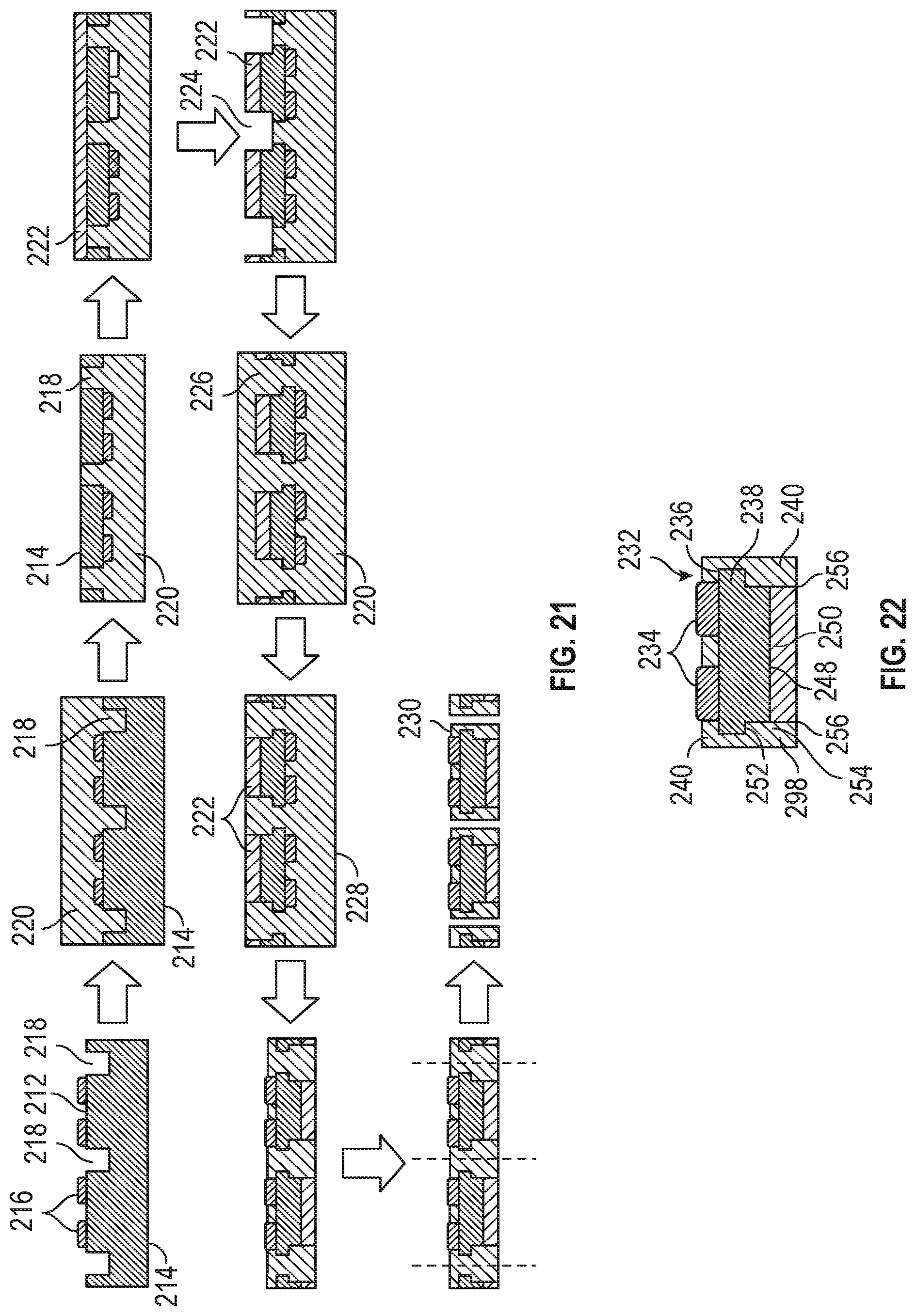
D00014
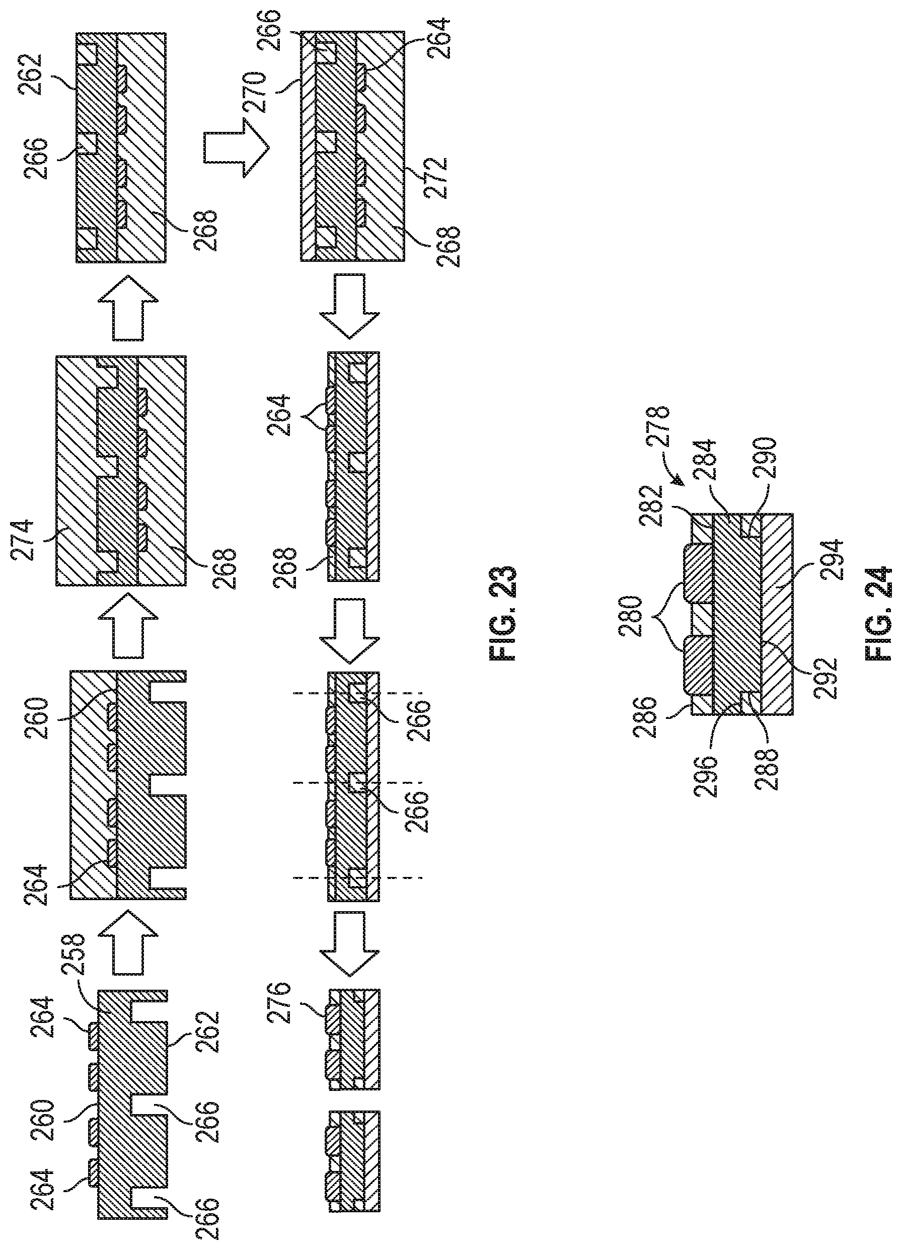
D00015
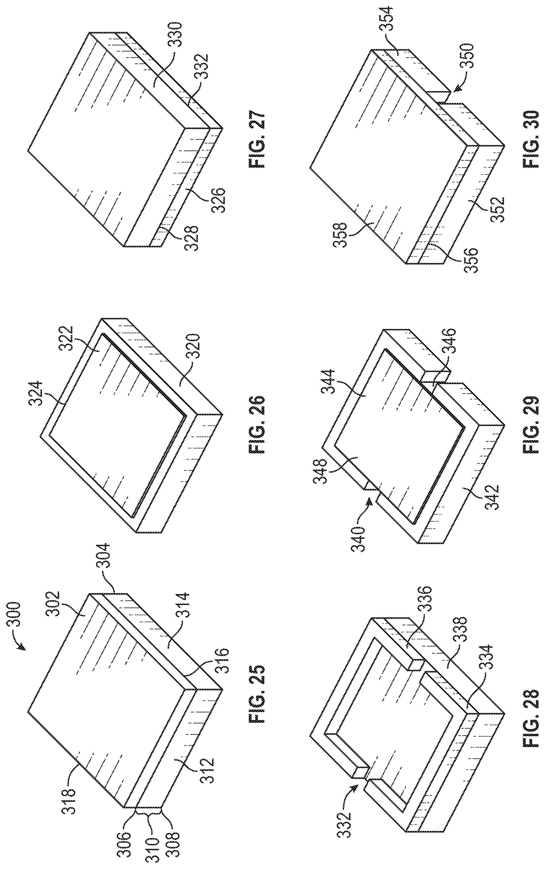
D00016
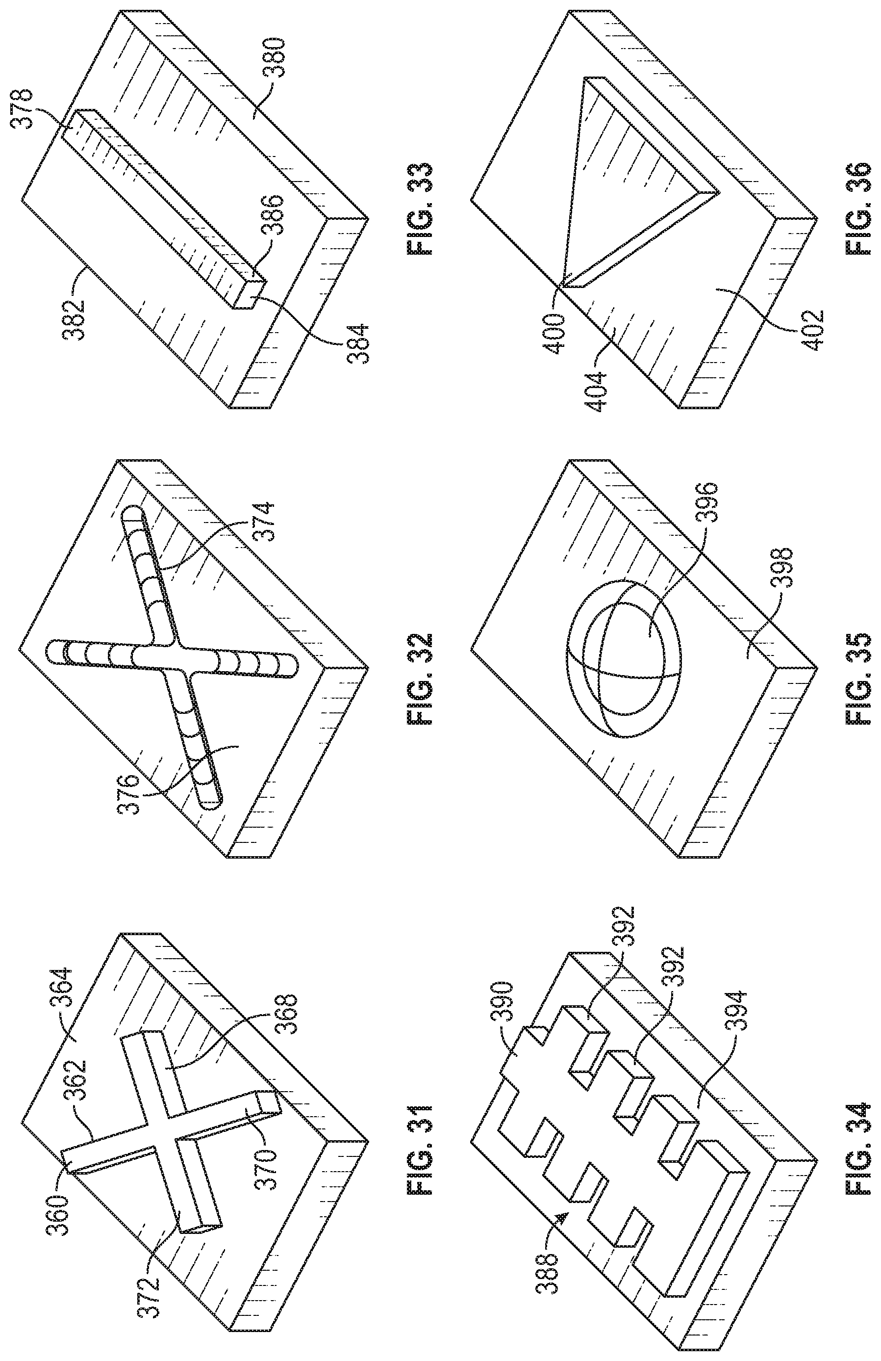
D00017
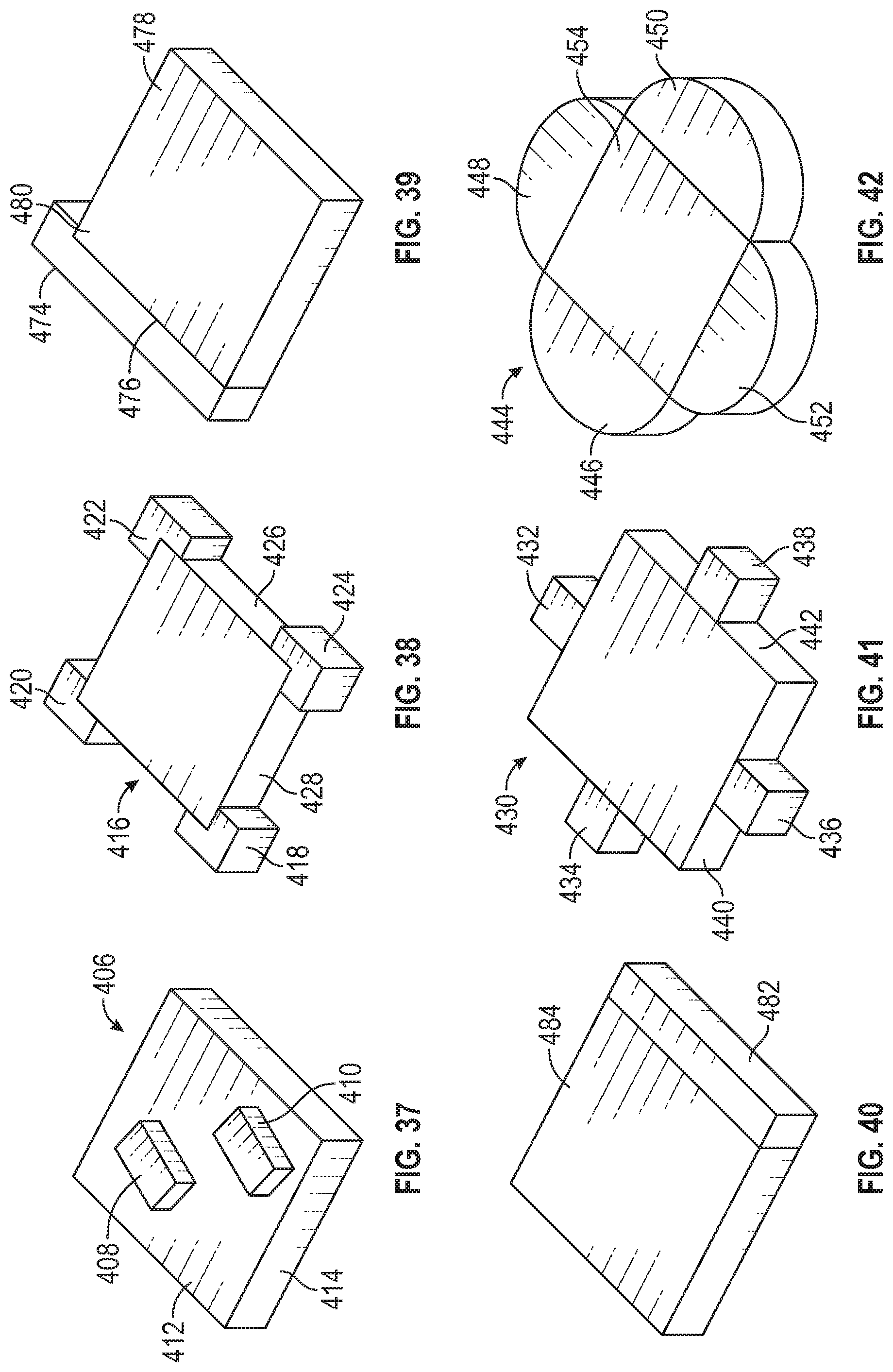
D00018
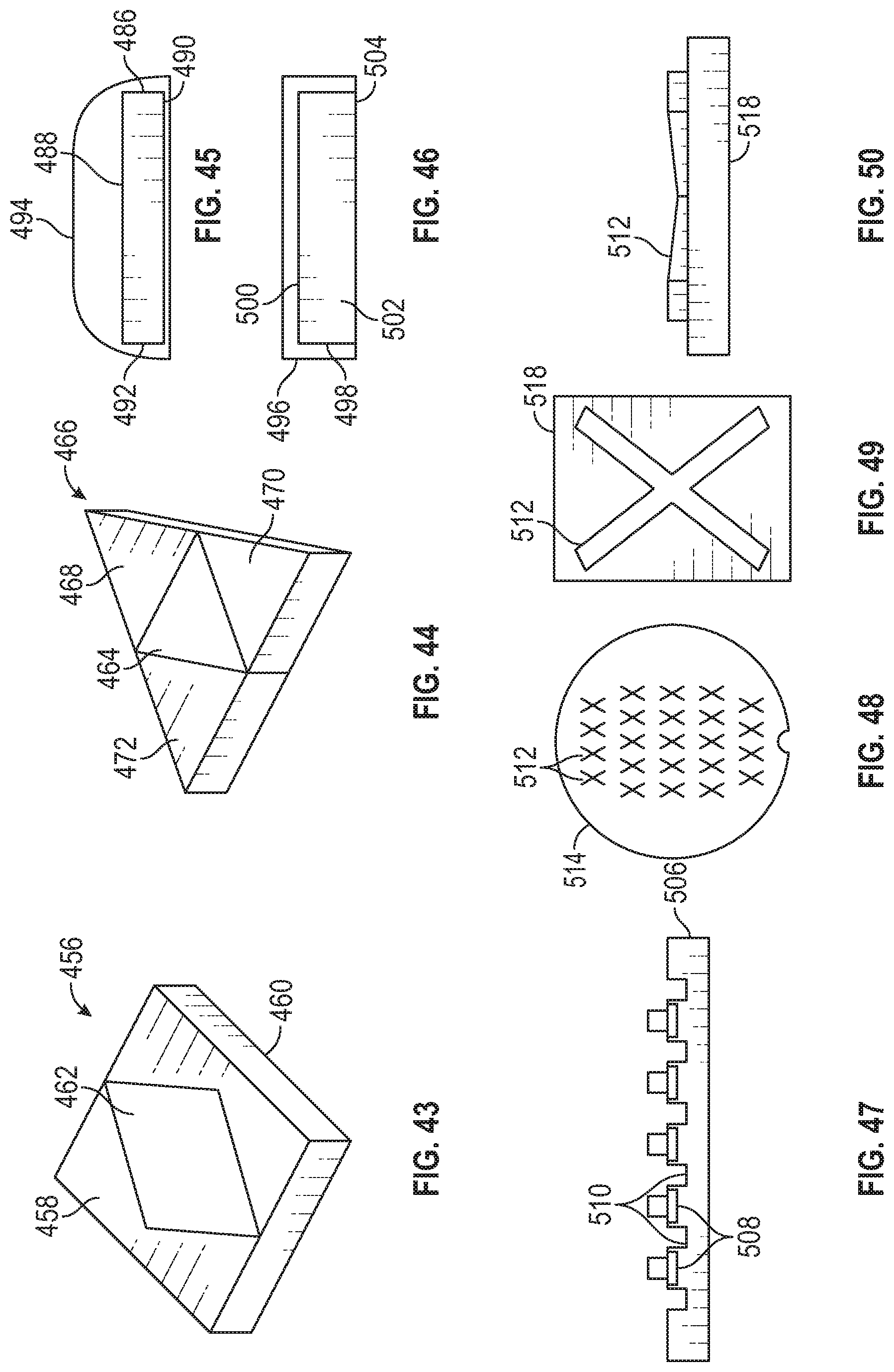
D00019
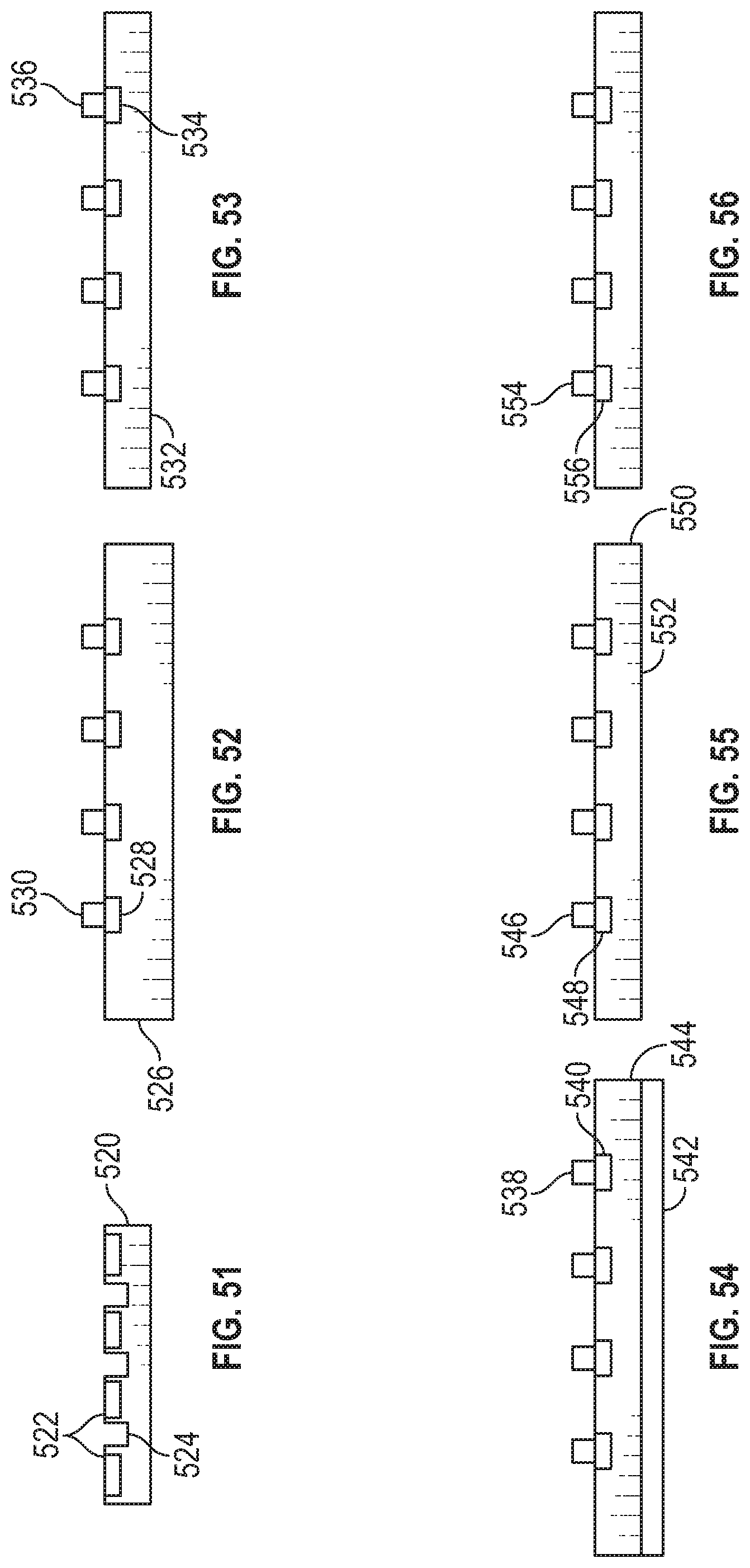
XML
uspto.report is an independent third-party trademark research tool that is not affiliated, endorsed, or sponsored by the United States Patent and Trademark Office (USPTO) or any other governmental organization. The information provided by uspto.report is based on publicly available data at the time of writing and is intended for informational purposes only.
While we strive to provide accurate and up-to-date information, we do not guarantee the accuracy, completeness, reliability, or suitability of the information displayed on this site. The use of this site is at your own risk. Any reliance you place on such information is therefore strictly at your own risk.
All official trademark data, including owner information, should be verified by visiting the official USPTO website at www.uspto.gov. This site is not intended to replace professional legal advice and should not be used as a substitute for consulting with a legal professional who is knowledgeable about trademark law.