Tall Trenches For Via Chamferless And Self Forming Barrier
MIGNOT; Yann ; et al.
U.S. patent application number 16/197558 was filed with the patent office on 2020-05-21 for tall trenches for via chamferless and self forming barrier. The applicant listed for this patent is International Business Machines Corporation. Invention is credited to Yann MIGNOT, Hosadurga SHOBHA, Chih-Chao YANG.
| Application Number | 20200161180 16/197558 |
| Document ID | / |
| Family ID | 70727126 |
| Filed Date | 2020-05-21 |

| United States Patent Application | 20200161180 |
| Kind Code | A1 |
| MIGNOT; Yann ; et al. | May 21, 2020 |
TALL TRENCHES FOR VIA CHAMFERLESS AND SELF FORMING BARRIER
Abstract
Chamferless via structures and methods of manufacture are provided. The structures include a conductive line and a set of chamferless wiring vias formed in a dielectric material with at least one of the vias in contact with the conductive line. The set of chamferless wiring vias is formed with at least a first subset of wiring vias of a first height and a second subset of wiring vias of a second height. The method includes filling trenches within a substrate with a conductive material to form a set of wiring vias with a first height. Next, a block mask is used over a capping material layer to expose a portion of the conductive material layer. The capping material and the conductive material of the set of wiring vias defined by the block mask are etched forming a subset of wiring vias of the second height.
| Inventors: | MIGNOT; Yann; (Slingerlands, NY) ; YANG; Chih-Chao; (Glenmont, NY) ; SHOBHA; Hosadurga; (Niskayuna, NY) | ||||||||||
| Applicant: |
|
||||||||||
|---|---|---|---|---|---|---|---|---|---|---|---|
| Family ID: | 70727126 | ||||||||||
| Appl. No.: | 16/197558 | ||||||||||
| Filed: | November 21, 2018 |
| Current U.S. Class: | 1/1 |
| Current CPC Class: | H01L 21/76829 20130101; H01L 21/76897 20130101; H01L 21/76885 20130101; H01L 21/31111 20130101; H01L 21/76849 20130101; H01L 21/76877 20130101; H01L 23/53209 20130101; H01L 23/528 20130101 |
| International Class: | H01L 21/768 20060101 H01L021/768; H01L 21/311 20060101 H01L021/311; H01L 23/528 20060101 H01L023/528; H01L 23/532 20060101 H01L023/532 |
Claims
1. (canceled)
2. A method for fabricating chamferless vias, the method comprising: receiving a substrate stack comprising a dielectric layer and a plurality of trenches formed therein, the plurality of trenches filled with a conductive material to form a set of wiring vias with a first height; using a block mask over a capping material layer to expose a portion of the conductive material in contact with a subset of the set of wiring vias to etch to a second height; etching the capping material layer and the conductive material of the set of wiring vias defined by the block mask, thereby forming a subset of wiring vias of the second height in response to the etching and a subset of wiring vias of the first height underneath the block mask; and depositing a cap layer in contact with the dielectric layer and the set of wiring vias.
3. The method of claim 2, further comprising: removing the block mask; and forming a barrier using selective deposition to protect the subset of wiring vias of the second height.
4. The method of claim 3, wherein the barrier is formed using cobalt, titanium, or a combination thereof
5. The method of claim 3, further comprising: depositing a dielectric material over the cap layer and the barrier; forming a photolithographic patterning stack comprising at least a hard mask layer formed on one or more underlayers and a photoresist layer formed on and in contact with the hard mask layer; etching the photolithographic patterning stack to reveal a top portion of the set of wiring vias of the first height; and depositing a conductive layer formed on the top portion of the set of wiring vias of the first height.
6. The method of claim 5, wherein the dielectric material deposited over the cap layer and the barrier is an ultra-low k dielectric layer.
7. The method of claim 5, where the hard mask layer comprises one or more of SiO.sub.2, SiCOH, and TiN.
8. The method of claim 5, wherein the conductive material and the conductive layer are different materials.
9. The method of claim 5, wherein the conductive material and the conductive layer are identical materials.
10. The method of claim 5, wherein at least one of the set of wiring vias is further formed within an organic planarization layer above the dielectric material and extends through the hard mask layer and an etch stop material to expose an underlying metal material.
11. The method of claim 2, wherein the dielectric layer comprises an ultra-low-k material.
12. The method of claim 2, wherein the conductive material is copper, aluminum, tungsten, cobalt, tantalium, hafnium, ruthenium, or any combination thereof.
13. (canceled)
14. A structure comprising: a conductive line; a set of chamferless wiring vias formed in a dielectric material, the set of chamferless wiring vias are trenches filed with a conductive material, with at least one of the set of chamferless wiring vias in contact with the conductive line, the set of chamferless wiring vias formed with at least a first subset of wiring vias of a first height and a second subset of wiring vias of a second height, wherein the dielectric material comprises an ultra-low-k material; and a barrier over the second subset of wiring vias of the second height.
15. The structure of claim 14, wherein the barrier is formed using cobalt, titanium, or a combination thereof.
16. The structure of claim 14, wherein the set of chamferless wiring vias is copper, aluminum, tungsten, cobalt, tantalium, hafnium, ruthenium, or any combination thereof.
17. The structure of claim 14, further comprising: a top metal layer in contact with at least one of the set of chamferless wiring vias.
18. The structure of claim 17, wherein the top metal layer is a different material than the set of chamferless wiring vias.
19. The structure of claim 17, wherein the top metal layer is an identical material to the set of chamferless wiring vias.
20. An integrated circuit comprising at least: one or more semiconductor structures, wherein at least one of the one or more semiconductor structures comprises: a substrate; a dielectric material formed on the substrate; a conductive line; a set of chamferless wiring vias formed in the dielectric material, the set of chamferless wiring vias are trenches filed with a conductive material, with at least one of the set of chamferless wiring vias in contact with the conductive line, the set of chamferless wiring vias formed with at least a first subset of wiring vias of a first height and a second subset of wiring vias of a second height, wherein the dielectric material comprises an ultra-low-k material; and a barrier over the second subset of wiring vias of the second height.
21. The integrated circuit of claim 20, wherein the barrier is formed using cobalt, titanium, or a combination thereof.
22. The integrated circuit of claim 20, wherein the set of chamferless wiring vias is copper, aluminum, tungsten, cobalt, tantalium, hafnium, ruthenium, or any combination thereof.
Description
BACKGROUND OF THE INVENTION
[0001] The invention relates to semiconductor structures and, more particularly, to chamferless via structures and methods of manufacture.
[0002] Integrated circuits (ICs) typically include a plurality of semiconductor devices and interconnect wiring. Networks of metal interconnect wiring typically connect the semiconductor devices from a semiconductor portion of a semiconductor substrate. Multiple levels of metal interconnect wiring above the semiconductor portion of the semiconductor substrate are connected together to form a back-end-of-the line (BEOL) interconnect structure.
[0003] Several developments have contributed to increased performance of contemporary ICs. One such development is technology scaling which results in higher integration of structures, e.g., transistors, wiring, etc. However, technology scaling has posed several challenges including, e.g., process variation, stricter design rules, etc. For example, in trench first via last metal hard mask integration schemes, excessive non-self-aligned via (Non-SAV) chamfering can result during trench formation. This integration scheme results in chamfering which is very difficult to control, and can result in poor yields, jagged surfaces and shorting issues.
SUMMARY OF THE INVENTION
[0004] In one embodiment, a method for fabricating chamferless vias is disclosed. The method comprises receiving a substrate stack comprising a dielectric layer and a plurality of trenches formed therein. The plurality of trenches are filled with a conductive material to form a set of wiring vias with a first height (M1+V1). Next, a block mask is used over a capping material layer to expose a portion of the conductive material in contact with a subset of the set of wiring vias to etch to a second height (M1). The capping material layer and the conductive material are etched and a set of wiring vias are defined by the block mask, thereby forming a subset of wiring vias of the second height (M1) in response to the etching and a subset of wiring vias of the first height (M1+V1) underneath the block mask. The dielectric layer may be an ultra-low-k material. The conductive material a set of metallic element such as Copper, Aluminum, Tungsten, Hf, Ru, Ti, and Ta.
[0005] In another embodiment, a structure is disclosed. The structure comprises a conductive line and a set of chamferless wiring vias formed in a dielectric material with at least one of the set of chamferless wiring vias in contact with the conductive line. The set of chamferless wiring vias is formed with at least a first subset of wiring vias of a first height and a second subset of wiring vias of a second height. A barrier is formed over the second subset of wiring vias of the second height.
[0006] In a further embodiment, an integrated circuit is disclosed. The integrated circuit comprises one or more semiconductor structures. At least one of the one or more semiconductor structures comprises a conductive line and a set of chamferless wiring vias formed in a dielectric material with at least one of the set of chamferless wiring vias in contact with the conductive line. The set of chamferless wiring vias is formed with at least a first subset of wiring vias of a first height and a second subset of wiring vias of a second height. A barrier is formed over the second subset of wiring vias of the second height.
BRIEF DESCRIPTION OF THE DRAWINGS
[0007] The accompanying figures where like reference numerals refer to identical or functionally similar elements throughout the separate views, and which together with the detailed description below are incorporated in and form part of the specification, serve to further illustrate various embodiments and to explain various principles and advantages all in accordance with the present invention, in which:
[0008] FIGS. 1A through 1C is a cross-sectional view of one example of prior art photolithographic patterning stack according to one embodiment of the present invention;
[0009] FIGS. 2A through 2C is a cross-sectional view of one example of the overall overview process for photolithographic patterning stack according to one embodiment of the present invention;
[0010] FIGS. 3A through 3C is a cross-sectional view of the first major process steps in the overall overview process for photolithographic patterning stack of FIG. 2;
[0011] FIGS. 4A through 4B is a cross-sectional view of the second major process steps in the overall overview process for photolithographic patterning stack of FIG. 2;
[0012] FIG. 5 is a cross-sectional view of the third major process steps in the overall overview process for photolithographic patterning stack of FIG. 2;
[0013] FIG. 6 is a cross-sectional view of the fourth major process steps in the overall overview process for photolithographic patterning stack of FIG. 2;
[0014] FIGS. 7A through 7B is a cross-sectional view of the fifth major process steps in the overall overview process for photolithographic patterning stack of FIG. 2;
[0015] FIG. 8 is a cross-sectional view of the sixth major process steps in the overall overview process for photolithographic patterning stack of FIG. 2; and
[0016] FIG. 9 is a flow chart depicting a method for forming chamferless vias in accordance with at least one embodiment of the present invention.
DETAILED DESCRIPTION
[0017] It is to be understood that the present disclosure will be described in terms of a given illustrative architecture; however, other architectures, structures, substrate materials, process features, and steps may be varied within the scope of the present disclosure.
[0018] It will also be understood that when an element such as a layer, region or substrate is referred to as being "on" or "over" another element, it can be directly on the other element or intervening elements may also be present. In contrast, when an element is referred to as being "directly on" or "directly over" another element, there are no intervening elements present. It will also be understood that when an element is referred to as being "connected" or "coupled" to another element, it can be directly connected or coupled to the other element or intervening elements may be present. In contrast, when an element is referred to as being "directly connected" or "directly coupled" to another element, there are no intervening elements present.
[0019] The present disclosure may include a design for an integrated circuit chip that may be created in a graphical computer programming language and stored in a computer storage medium (such as a disk, tape, physical hard drive, or virtual hard drive such as in a storage access network). If the designer does not fabricate chips or the photolithographic masks used to fabricate chips, the designer may transmit the resulting design by physical means (e.g., by providing a copy of the storage medium storing the design) or electronically (e.g., through the Internet) to such entities, directly or indirectly. The stored design is then converted into the appropriate format (e.g., GDSII) for the fabrication of photolithographic masks, which typically include multiple copies of the chip design in question that are to be formed on a wafer. The photolithographic masks are utilized to define areas of the wafer (and/or the layers thereon) to be etched or otherwise processed.
[0020] Methods as described herein may be used in the fabrication of integrated circuit chips. The resulting integrated circuit chips can be distributed by the fabricator in raw wafer form (that is, as a single wafer that has multiple unpackaged chips), as a bare die, or in a packaged form. In the latter case the chip is mounted in a single chip package (such as a plastic carrier, with leads that are affixed to a motherboard or other higher-level carrier) or in a multichip package (such as a ceramic carrier that has either or both surface interconnections or buried interconnections). In any case the chip is then integrated with other chips, discrete circuit elements, and/or other signal processing devices as part of either (a) an intermediate product, such as a motherboard, or (b) an end product. The end product can be any product that includes integrated circuit chips, ranging from toys and other low-end applications to advanced computer products having a display, a keyboard or other input device, and a central processor.
[0021] Reference in the specification to "one embodiment" or "an embodiment" of the present principles, as well as other variations thereof, means that a particular feature, structure, characteristic, and so forth described in connection with the embodiment is included in at least one embodiment of the present principles. Thus, the appearances of the phrase "in one embodiment" or "in an embodiment", as well any other variations, appearing in various places throughout the specification are not necessarily all referring to the same embodiment.
[0022] The invention relates to semiconductor structures and, more particularly, to chamferless via structures and methods of manufacture during back end of the line (BEOL) processing. Advantageously, the processes described herein will result in final wiring structures.
[0023] The chamferless via structures of the present invention may be manufactured in a number of ways using a number of different tools. In general, though, the methodologies and tools are used to form structures with dimensions in the micrometer and nanometer scale. The methodologies, i.e., technologies, employed to manufacture the chamferless via structures of the present invention have been adopted from integrated circuit (IC) technology. For example, the structures of the present invention are built on wafers and are realized in films of material patterned by photolithographic processes on the top of a wafer. In particular, the fabrication of the chamferless via structures of the present invention uses three basic building blocks: (i) deposition of thin films of material on a substrate, (ii) applying a patterned mask on top of the films by photolithographic imaging, and (iii) etching the films selectively to the mask.
[0024] There are several overall aspects to the present invention. The first aspect is that there is a tall trench formation. The tall trench is the M1 height plus the V1 height. M1 is lower portion of a wiring via and the V2 an upper portion of the wiring via. A portion of the via defined by length V2 is sticking out after the M1 recess. The second aspect is the lithography for the via is a block mask using a save and cut approach. The portion of the via M2 is a trench type only. The third aspect is that the present invention does not require a self-aligned via (SAV) or full aligned via (FAV). The fourth aspect is that the via mask is a block and this may be easier to manufacture since it covers only the oxide area. The fifth aspect is that the present invention uses a self-formation barrier.
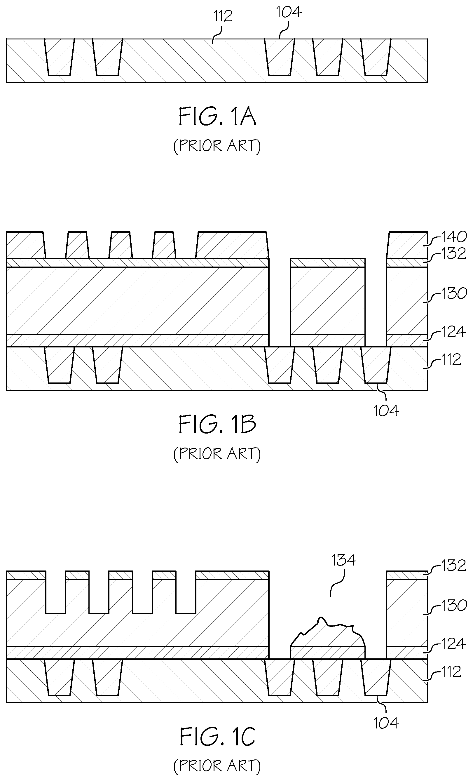
[0025] Now referring to the figures, shown in FIGS. 1A through 1C are cross-sectional views of one example of prior art photolithographic patterning stack according to one embodiment of the present invention. Starting with FIG. 1A shown is a M1 wiring via portion in substrate stack with conductive areas 104 comprising a dielectric layer 112. FIG. 1B is photolithographic patterning stack. A protective liner 124 is formed to cover the conductive areas 104 and dielectric layer 112 as shown. A ultra-low K material layer 130 is formed over a protective liner 124. A hard mask (HM) layer 132, such as TiN, and an Oxide mask 140 are formed on the ultra-low K dielectric 130 .The process completes with metallization not drawn with a view of the degraded chamfer 134 as shown in FIG. 1C. Typically, the metallization forms a bridge between two conductive areas 104 with a chamfer.
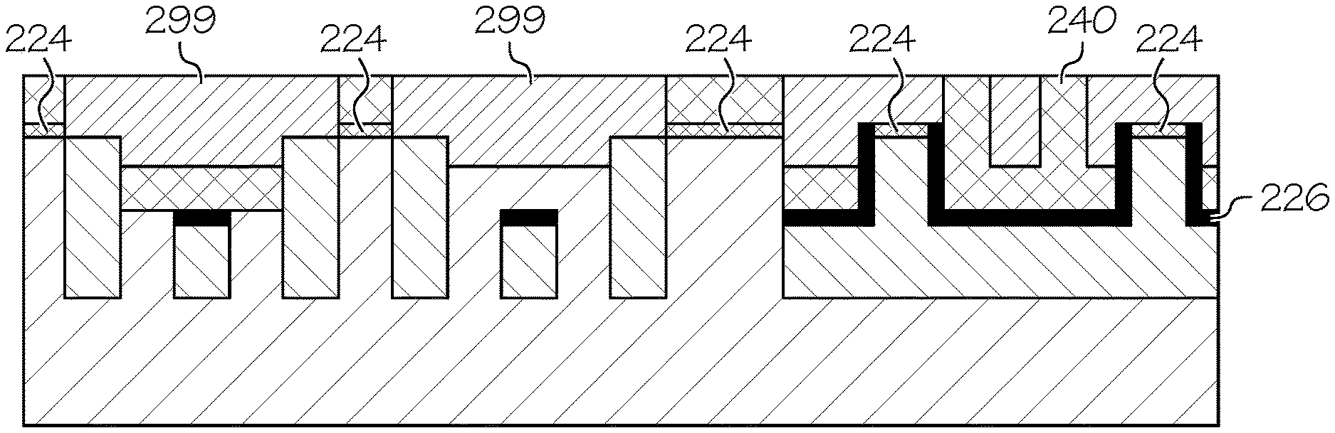
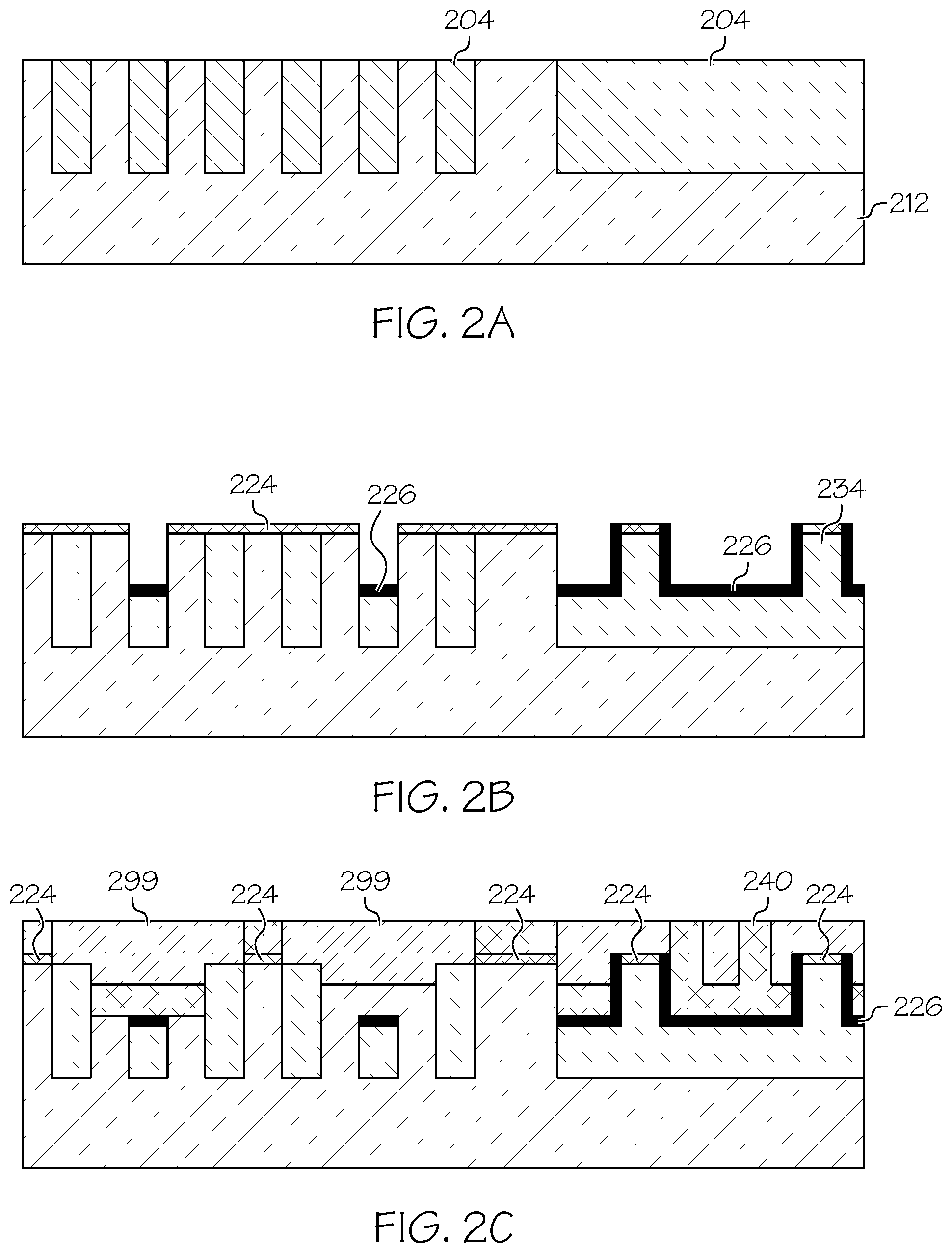
[0026] FIGS. 2A through 2C are cross-sectional views of one example of the overall overview process for photolithographic patterning stack according to one embodiment of the present invention. Shown is a M1 wiring via portion and V1 via portion 204 which is conductive in a dielectric layer 212. The overall via M1+V1 is two to three times smaller. In one example the overall via has a M1 trench portion of approximately 45 nm and the V1 portion of about 30 nm. Other dimensions for M1 and V1 are possible within the true scope of the present invention. FIG. 2B illustrates cutting the via so only the mostly the M1 portion 236 remains and some of the V1 portions 234 sticking out of the dielectric layer 212. Also shown is a cap layer 224 and self-barrier formation 226. FIG. 2C illustrates the structure after the metallization 299. Notice this structure is very different that the prior art structure in FIG. 1C. More specifically, in FIG. 1C the via is defined by the top metal while by opposite the via are defined by the bottom metal in FIG. 2. In contrast, unlike the prior art structure of FIG. 1C, the metallization in the present invention can be the same for bother the top metal and the bottom metal or defined as two different metal layers base on the device requirement.
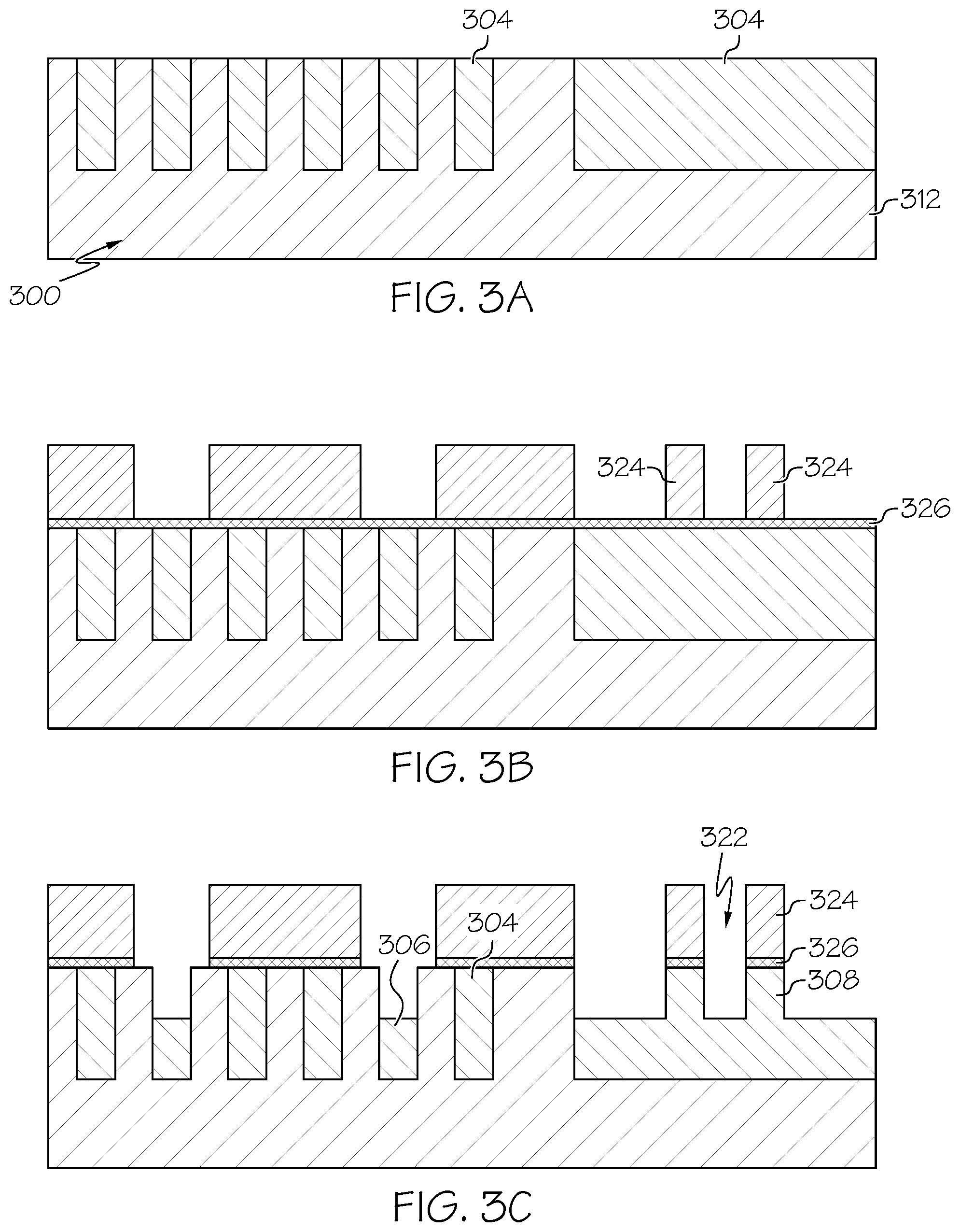
[0027] FIGS. 3A through 3C are cross-sectional views of the first major process steps in the overall overview process for photolithographic patterning stack of FIG. 2. The process starts with receiving a substrate stack comprising a dielectric layer 312 and a plurality of trenches formed therein. It is important to note that the substrate in some examples is a multilayer substrate with a structure that defines other functions of the overall integrated circuit or device. A substrate stack 312 may include a substrate with various layers formed thereon such as: (i) a porous, ultra-low-k (i.e., ultra-low dielectric constant) dielectric material ("ULK" or "ULK layer"); (ii) a hard mask layer comprising SiO2, SiCOH, and TiN, and/or another similarly suitable material overlying the ULK layer; and (iii) a conductive layer e.g., copper or tungsten, amongst other metal or metal alloys underlying the ULK layer. The ULK layer may be separated from the conductive layer by a cap (i.e., barrier) layer comprising another dielectric material, if it is not desired that the ULK layer come directly into contact with the conductive layer. Suitable materials for the cap layer may include, for example but without limitation, SiCN, SiN, SiC, SiCNH, and SiNO.
[0028] The dielectric layer 312 may be formed to a thickness of about 50 to 500 nm; although other dimensions are also contemplated by embodiments of the present invention. The dielectric layer 312 may be with low-K (UK) or ultra-low k (ULK) dielectric layer. The plurality of trenches are filled with a conductive material to form a set of wiring vias 304 with a first height (M1+V1).
[0029] FIG. 3B illustrates a cap layer 326 with a block mask 324 to define the cut area of the trench. In one example the cap layer is a Nblock cap layer 326. The Nblock cap layer 326 may be formed using conventional deposition processes, e.g., chemical vapor deposition (CVD), followed by lithographic process composed by a resist mask , anti-reflective coating such as Siarc and OPL layer 324 and etching, e.g., Reactive Ion Etching (RIE), wet etching or processes known to those of ordinary skill in the art such that further description is not required for an understanding of the invention. The lithography and etching process results in a self-aligned via structure as described herein.
[0030] In one or more embodiments, the openings e.g. 322 are formed by conventional lithography and etching processes. For example, a resist may be formed over the hard mask (not shown), which is exposed to energy (light) to form a pattern (openings). A reactive ion etching (RIE) process may then be performed through the openings of the resist to form the openings in the hard mask. The resist may then removed using conventional stripants or oxygen ashing processes.
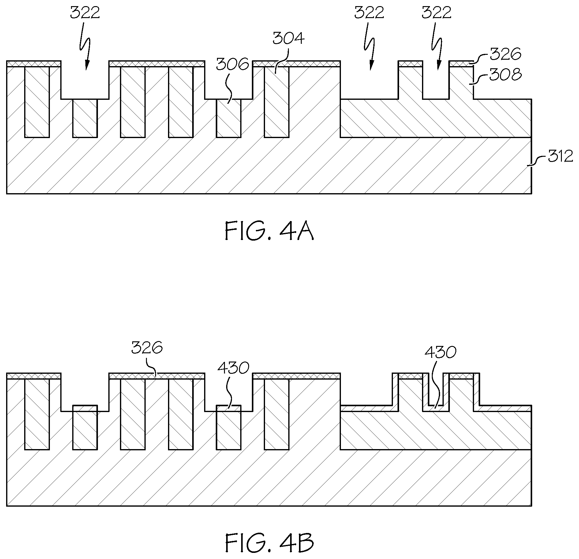
[0031] The OPL block mask 324 saves the via 304 in opening 322 but removes everything else through an etching step. As shown in FIG. 3C portions of the wiring vias 304 are removed using appropriate chemistry. Shown are examples of subsets of wiring vias 304 with two distinct heights: a first height M1+V1 308 underneath the block mask 324, and a second height M1 306. One example of the dry etching process chemistry will be the use of BCl3/Cl2 for Alumiunim or Titanium metal, SF6 or Cl2 for Tungsten metal, or any other gas chemistries known., Etch process stops at the M1 height.
[0032] FIG. 4A is a cross-sectional view of the second major process steps in the overall overview process for photolithographic patterning stack of FIG. 2. Block mask 324 is removed using a dry strip chemistry base on CO/CO2, or N2/H2 or example. In this way, the underlying cap layer 326, the wiring via 304 , the wiring via of second height M1 306, the wiring via of the first height M1+V1 308 and part of 312 around the via opening 322 are exposed.
[0033] FIG. 4B illustrates the next process of selective metal deposition for creating a self-barrier 430 is performed. The self-barrier 430 is a selective liner deposition is created by exposing the substrate surface to a cobalt containing precursor gas in a multi ALD or CVD deposition and treatment cycles process for example. The cobalt capping material layer will selectively form over the metallic feature surface while leaving the dielectric surface free of deposition. This self-barrier 430, in one example, is Cobalt (Co), Titanium (Ti) or a combination. Other metals may be used. The self-barrier layer 430 is optional base on the metal used for layer 304 but required for some metal such as Copper. The selective deposition layer is used to prevent metal migration into the dielectric layer 312 and act as a barrier mostly in case of M1 Copper for metal wiring vias 304.
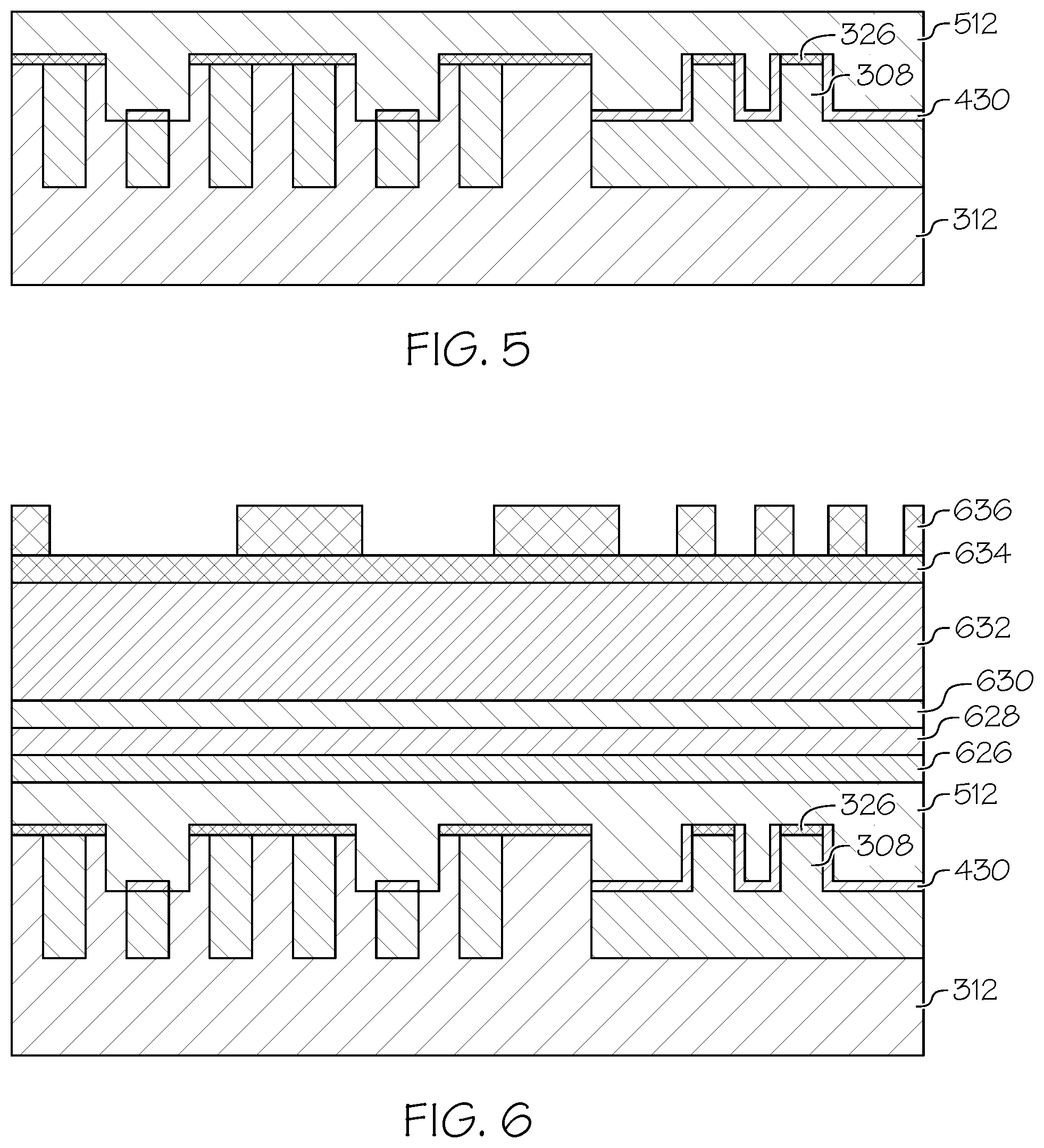
[0034] FIG. 5 shows a cross-sectional view of the third major process steps in the overall overview process for photolithographic patterning stack of FIG. 2. The third major process is dielectric layer 512 deposition. This dielectric layer 512 may be formed as a low-K (UK) or ultra-low k (ULK) dielectric layer. The dielectric 512 like the first Dielectric 312 may be deposited over the structure, e.g., cap 326 and self-barrier 430. In embodiments, the Dielectric layer 512 may be spun on and baked or may be deposited by CVD. The dielectric 512 may be baked at lower temperatures, such as 150-200.degree. C. to avoid damaging any other materials. The formation of the dielectric layer or dielectric 512 is followed by chemical-mechanical planarization (CMP). The dielectric layer 512, in one example, is the same material as 312. In another example the material 512 may be different material from the material 312.
[0035] FIG. 6 is a cross-sectional view of the fourth major process steps in the overall overview process for photolithographic patterning stack of FIG. 2. This process comprises multi-layer stack deposition with previous hard mask oxide (HMO) lithography. Shown is a first sacrificial layer 626 formed over the dielectric layer 512. FIG. 6 also shows a Titanium Nitride (TiN) layer 628 formed over the first sacrificial layer 626. Next, an oxide derived from TEOS (tetraethylorthosilicate) layer 630, a silicon oxide, a silane oxide, or a Si-containing ARC material (SiARC) may be deposited on top of TiN layer 628. Another organic planarization layer (OPL) layer 632 may be deposited over the TEOS layer 630. Next, a Si-rich anti-reflective coating (SiARC) layer 634 may be disposed on top of OPL layer 632 followed by the resist layer 636 defining the area to etch.
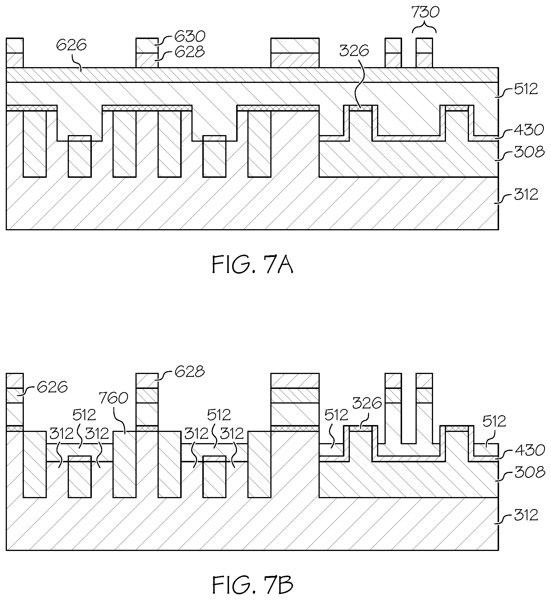
[0036] FIGS. 7A through 7B show a cross-sectional view of the fifth major process steps in the overall overview process for photolithographic patterning stack of FIG. 2. The resist layer 636 of FIG. 6 is used to form the pattern on TEOS 630 and TiN 628 forming stack 730 stopping on the first sacrificial layer 626. Resist layer 636, Siarc layer 634 and OPL layer 632 are etched away during that sequence. FIG. 7B illustrates etching the trench into dielectric 512 using RIE etch processes with stack 730 as mask. The process will etch the first sacrificial layer 626, top TEOS 636, part of the dielectric 512 to the desired height and the Cap layer 326. The trench dielectric 512 reveals some of the ULK trench with some over etch (OE) to reveal the top via 760.
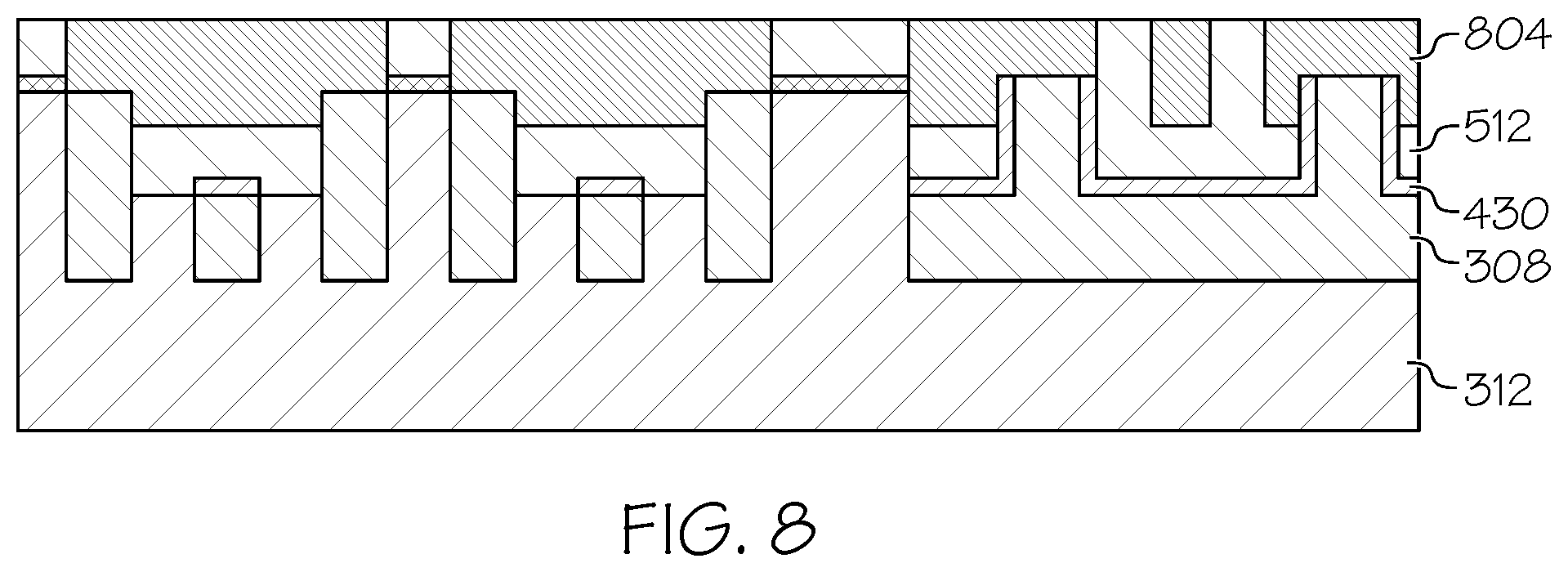
[0037] FIG. 8 is a cross-sectional view of the sixth major process steps in the overall overview process for photolithographic patterning stack of FIG. 2. In this step, metallization 804 is formed. The metallization may be the same material as metallization 304 or different material. A liner, which is not shown, may be situated below the metallization 804 all around previous structure. The metallization 804 may be a copper material formed by an electroplating process as is well known to those of skill in the art. In embodiments, prior to the metal fill process, any residual RIE material may be cleaned from the wiring via 304 and the trenches using a wet etch process, followed by deposition of a barrier and seed layer. Sacrificial layers 626 and TiN 628 used for patterning are removed by wet clean prior metallization 804 or after using a CMP process. The barrier layer may prevent metal diffusion into the ultra-low-k dielectric and it may promote seed layer adhesion. After the deposition of a barrier and seed layer, the electroplating process may commence to form metal lines, e.g., metal fill material 804. Any residual metal fill material 804 on a surface of the structure may be removed by a conventional planarization process. e.g., chemical mechanical polishing (CMP).
[0038] FIG. 9 is a flow chart illustrating one example of a method for forming chamferless vias in accordance with at least one embodiment of the present invention. As illustrated, the method starts at step 1002 and immediately proceeds to step 1004 in which a substrate stack is received e.g. 300 of FIG. 3. The substrate includes a dielectric layer and trenches formed therein. The trenches are filled with a conductive material to form a set of wiring vias 304 with a first height (M1+V1). A block mask, at step 1006, is used to expose a portion of the conductive material 304 and Nblock Cap layer 326 in contact with a subset of the set of wiring vias to etch to a second height (M1). The block mask, at step 1008, is removed. A selective barrier liner, at step 1010, is formed using selective deposition to protect the subset of wiring vias of the second height (M1) and to prevent migration of copper into oxide. In step 1012, the dielectric layer and the conductive material are etched. The etching forms a set of wiring vias defined by the block mask, thereby forming a subset of wiring vias of the second height (M1) in response to the etching and a subset of wiring vias of the first height (M1+V1). The process ends at step 1014.
[0039] The method(s) as described above is used in the fabrication of integrated circuit chips. The resulting integrated circuit chips can be distributed by the fabricator in raw wafer form (that is, as a single wafer that has multiple unpackaged chips), as a bare die, or in a packaged form. In the latter case the chip is mounted in a single chip package (such as a plastic carrier, with leads that are affixed to a motherboard or other higher level carrier) or in a multichip package (such as a ceramic carrier that has either or both surface interconnections or buried interconnections). In any case the chip is then integrated with other chips, discrete circuit elements, and/or other signal processing devices as part of either (a) an intermediate product, such as a motherboard, or (b) an end product. The end product can be any product that includes integrated circuit chips, ranging from toys and other low-end applications to advanced computer products having a display, a keyboard or other input device, and a central processor.
[0040] Although specific embodiments have been disclosed, those having ordinary skill in the art will understand that changes can be made to the specific embodiments without departing from the spirit and scope of the disclosure. The scope of the disclosure is not to be restricted, therefore, to the specific embodiments, and it is intended that the appended claims cover any and all such applications, modifications, and embodiments within the scope of the present disclosure.
[0041] It should be noted that some features of the present disclosure may be used in one embodiment thereof without use of other features of the present disclosure. As such, the foregoing description should be considered as merely illustrative of the principles, teachings, examples, and exemplary embodiments of the present disclosure, and not a limitation thereof.
[0042] Also note that these embodiments are only examples of the many advantageous uses of the innovative teachings herein. In general, statements made in the specification of the present application do not necessarily limit any of the various claimed disclosures. Moreover, some statements may apply to some inventive features but not to others.
* * * * *
D00000
D00001
D00002
D00003
D00004
D00005
D00006
D00007
D00008
XML
uspto.report is an independent third-party trademark research tool that is not affiliated, endorsed, or sponsored by the United States Patent and Trademark Office (USPTO) or any other governmental organization. The information provided by uspto.report is based on publicly available data at the time of writing and is intended for informational purposes only.
While we strive to provide accurate and up-to-date information, we do not guarantee the accuracy, completeness, reliability, or suitability of the information displayed on this site. The use of this site is at your own risk. Any reliance you place on such information is therefore strictly at your own risk.
All official trademark data, including owner information, should be verified by visiting the official USPTO website at www.uspto.gov. This site is not intended to replace professional legal advice and should not be used as a substitute for consulting with a legal professional who is knowledgeable about trademark law.