Enhanced Anodization For Processing Equipment
HE; Xiao-Ming ; et al.
U.S. patent application number 16/433990 was filed with the patent office on 2019-12-12 for enhanced anodization for processing equipment. The applicant listed for this patent is Applied Materials Inc.. Invention is credited to Cheng-Hsuan CHOU, David FENWICK, Xiao-Ming HE, Chidambara A. RAMALINGAM, Michael R. RICE, Jennifer Y. SUN, Xiaowei WU.
| Application Number | 20190376202 16/433990 |
| Document ID | / |
| Family ID | 68764674 |
| Filed Date | 2019-12-12 |


| United States Patent Application | 20190376202 |
| Kind Code | A1 |
| HE; Xiao-Ming ; et al. | December 12, 2019 |
ENHANCED ANODIZATION FOR PROCESSING EQUIPMENT
Abstract
An enhanced anodization method includes forming a porous anodization layer comprising columns of anodization layer material with pores between adjacent columns. The method further includes sealing the porous layer by forming a sealing layer at a top of the porous layer. The sealing layer may be formed by using a hybrid sealing process that combines, in any order, two or more of de-ionized (DI) water seal, Ni sealing, and, PTFE sealing. Alternatively, the sealing layer is formed by conformally coating the columns in the porous layer with one or more layers of a coating material. Further, the coating material may be surface-fluorinated to improve plasma resistance.
| Inventors: | HE; Xiao-Ming; (Fremont, CA) ; SUN; Jennifer Y.; (Mountain View, CA) ; FENWICK; David; (Los Altos, CA) ; CHOU; Cheng-Hsuan; (Santa Clara, CA) ; WU; Xiaowei; (San Jose, CA) ; RAMALINGAM; Chidambara A.; (Fremont, CA) ; RICE; Michael R.; (Pleasanton, CA) | ||||||||||
| Applicant: |
|
||||||||||
|---|---|---|---|---|---|---|---|---|---|---|---|
| Family ID: | 68764674 | ||||||||||
| Appl. No.: | 16/433990 | ||||||||||
| Filed: | June 6, 2019 |
Related U.S. Patent Documents
| Application Number | Filing Date | Patent Number | ||
|---|---|---|---|---|
| 62683379 | Jun 11, 2018 | |||
| Current U.S. Class: | 1/1 |
| Current CPC Class: | C25D 11/18 20130101; C25D 11/06 20130101; C25D 11/20 20130101; C25D 11/246 20130101 |
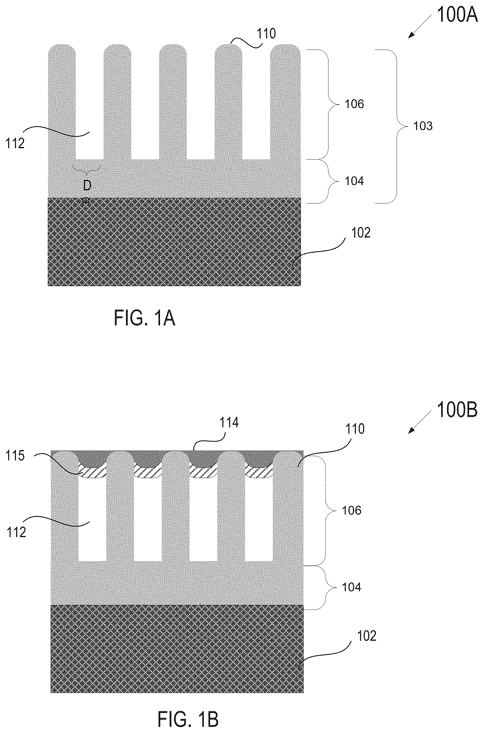
| International Class: | C25D 11/24 20060101 C25D011/24; C25D 11/20 20060101 C25D011/20 |
Claims
1. A method of manufacturing a chamber component for a processing chamber, the method comprising: providing a metallic article, wherein the metallic article is a part of the chamber component; anodizing the metallic article by forming an anodization layer on the metallic article, wherein the anodization layer comprises a barrier layer adjacent to an external surface of the metallic article and a porous layer on top of the barrier layer, the porous layer comprising columns of anodization layer material with pores between adjacent columns; and sealing the porous layer by forming a sealing layer at a top of the porous layer, wherein the sealing layer is formed using a hybrid sealing process that comprises combining, in any order, two or more of the following sealing processes: a first sealing process comprising sealing with de-ionized (DI) water steam; a second sealing process comprising sealing with nickel plating; and a third sealing process comprising sealing with polytetrafluoroethylene (PTFE).
2. The method of claim 1, wherein the first sealing process forms hydrated metallic oxide.
3. The method of claim 1, wherein performing the second sealing process comprises immersing the metallic article in a nickel acetate solution.
4. The method of claim 1, wherein performing the third sealing process comprises spraying, dipping or brushing a thermosetting resin containing PTFE onto the anodized metallic article.
5. A method of manufacturing a chamber component for a processing chamber, the method comprising: providing a metallic article, wherein the metallic article is a part of the chamber component; anodizing the metallic article by forming an anodization layer on the metallic article, wherein the anodization layer comprises a barrier layer adjacent to an external surface of the metallic article and a porous layer on top of the barrier layer, the porous layer comprising columns of anodization layer material with pores between adjacent columns; and sealing the porous layer by forming a sealing layer at a top of the porous layer, wherein the sealing layer is formed by conformally coating the columns in the porous layer with one or more layers of a coating material.
6. The method of claim 5, wherein sealing the porous layer further comprises: annealing the one or more layers of the coating material to form a surface alloy of the coating material.
7. The method of claim 5, wherein the one or more layers of the coating material are deposited using one or more of the following processes: atomic layer deposition (ALD), physical vapor deposition (PVD), chemical vapor deposition (CVD), plasma enhanced chemical vapor deposition (PECVD), plasma enhanced physical vapor deposition (PEPVD), and wet chemical deposition.
8. The method of claim 7, wherein a thickness of the sealing layer is selected such that the one or more layers of the coating material fully fill the pores between adjacent columns.
9. The method of claim 7, wherein a thickness of the sealing layer is selected such that the one or more layers of the coating material partially fill the pores between adjacent columns.
10. The method of claim 9, wherein a pore size for the pores between the coated columns of the porous layer is in the range of 5-60 nm.
11. The method of claim 5, wherein the coating material comprises an oxide, the method further comprising: conducting in-situ fluorination to replace at least a portion of oxygen molecules of the oxide with fluorine molecules and convert at least a surface of the coating from the oxide into a fluoride or an oxy-fluoride.
12. The method of claim 11, wherein the coating material is Al.sub.2O.sub.3 or Y.sub.2O.sub.3, and the surface of the coating is converted to AlF.sub.3/AlOF or YF.sub.3/YOF after in-situ fluorination.
13. The method of claim 12, wherein performing the in-situ fluorination comprises: immersing the article in a mixed acid solution containing HF, NH.sub.4F, and H.sub.2O.sub.2 in predetermined volumetric ratio.
14. The method of claim 12, wherein performing the in-situ fluorination comprises: irradiating the article with a fluorine-containing plasma.
15. A chamber component for a processing chamber, comprising: a metallic article that is a part of the chamber component; an anodization layer formed on the metallic article, wherein the anodization layer comprises a barrier layer adjacent to an external surface of the metallic article and a porous layer on top of the barrier layer, the porous layer comprising columns of anodization layer material with pores between adjacent columns; and a hybrid sealing layer formed at a top of the porous layer, wherein the hybrid sealing layer comprises, in any order, two or more of the following layers: a hydrated metallic oxide layer; a plated nickel layer; and a polytetrafluoroethylene (PTFE) layer.
16. A chamber component for a processing chamber, comprising: a metallic article that is a part of the chamber component; an anodization layer formed on the metallic article, wherein the anodization layer comprises a barrier layer adjacent to an external surface of the metallic article and a porous layer on top of the barrier layer, the porous layer comprising columns of anodization layer material with pores between adjacent columns; and a sealing layer formed at a top of the porous layer, wherein the sealing layer comprises one or more layers of a coating material conformally deposited onto the columns in the porous layer.
17. The chamber component of claim 16, wherein the thickness of the sealing layer is selected such that the one or more layers of the coating material fully fill the pores between adjacent columns.
18. The chamber component of claim 16, wherein the thickness of the sealing layer is selected such that the one or more layers of the coating material partially fill the pores between adjacent columns.
19. The chamber component of claim 17, wherein a pore size for the pores between the coated columns of the porous layer is in the range of 5-60 nm.
20. The chamber component of claim 16, wherein the sealing layer further comprises: a fluorinated outer surface layer over the one or more layers of the coating material.
Description
RELATED APPLICATION
[0001] This application is related to and claims the benefit of U.S. Provisional Patent Application No. 62/683,379, filed on Jun. 11, 2018, the entirety of which is incorporated herein by reference.
TECHNICAL FIELD
[0002] Embodiments of the present disclosure relate, in general, to anodized metallic articles and to a process for applying a sealing layer to an anodized article.
BACKGROUND
[0003] In the semiconductor industry, devices are fabricated by a number of manufacturing processes producing structures of an ever-decreasing size. Some manufacturing processes such as plasma etch may generate particles and metal contamination from the processing chamber that adversely affect a substrate that is being processed, contributing to device defects. As device geometries shrink, susceptibility to these defects increases, and particle and metal contamination requirements become more stringent. Accordingly, as device geometries shrink, allowable levels of particle defects and metal contamination may be reduced significantly. Degradation of processing chamber components may also destabilize the plasma within the processing chamber. Therefore, plasma resistant chamber components are advantageous.
SUMMARY
[0004] Methods of manufacturing a chamber component for a processing chamber using an enhanced anodization processes are disclosed. The processing chamber may be used inside a plasma generator source (including a remote plasma source (RPS)) and/or other chambers used for plasma etching or other processes. An anodization process is enhanced by combining anodization with innovating sealing techniques. An enhanced anodization method includes first anodizing a metallic article by forming an anodization layer on the metallic article. The metallic article may be a chamber component or a part of a chamber component. The anodization layer comprises a barrier layer adjacent to an external surface of the metallic article and a porous anodization layer on top of the barrier layer. The porous anodization layer comprises columns of anodization layer material with pores between adjacent columns. The method further includes sealing the porous anodization layer by forming a sealing layer at a top of the porous anodization layer.
[0005] In one embodiment, the sealing layer is formed using a hybrid sealing process that comprises combining, in any order, two or more different sealing processes. The sealing processes include sealing with de-ionized (DI) water steam, sealing with nickel plating, and sealing with polytetrafluoroethylene (PTFE).
[0006] In another embodiment, the sealing layer is formed by conformally coating the columns in the porous anodization layer with one or more layers of a coating material. The coating material may be an oxide. In-situ fluorination may be conducted to replace at least a portion of oxygen molecules of the oxide with fluorine molecules and convert at least a surface of the conformal coating from the oxide into a fluoride or an oxy-fluoride.
[0007] Also disclosed is a chamber component for a processing chamber, the chamber component having a metallic article that is anodized and sealed according to the methods disclosed here.
[0008] The thickness of the sealing layer is selected such that the one or more layers of the coating material fully or partially fill the pores between adjacent columns. When partially filled, a pore size for the pores between the coated columns of the porous layer may be in the range of 5-60 nm.
[0009] The resulting anodized and sealed metallic articles show superior stability against plasma erosion as compared to metallic articles manufactured using conventional anodization and sealing techniques. Additionally, the resulting anodized and sealed metallic articles have been shown to introduce minimal contamination to semiconductor wafers being processed in a processing chamber that contains the metallic articles that have been anodized and sealed in accordance with embodiments of the present disclosure.
BRIEF DESCRIPTION OF THE DRAWINGS
[0010] The present disclosure is illustrated by way of example, and not by way of limitation, in the figures of the accompanying drawings in which like references indicate similar elements. It should be noted that different references to "an" or "one" embodiment in this disclosure are not necessarily to the same embodiment, and such references mean at least one.
[0011] FIG. 1A illustrates an anodized chamber component for use in a semiconductor manufacturing chamber, in accordance with one embodiment of the present disclosure.
[0012] FIG. 1B illustrates an anodized and hybridly sealed chamber component for use in a semiconductor manufacturing chamber, in accordance with one embodiment of the present disclosure.
[0013] FIG. 1C illustrates an anodized and hybridly sealed chamber component for use in a semiconductor manufacturing chamber, in accordance with another embodiment of the present disclosure.
[0014] FIG. 2 illustrates an exemplary architecture of a manufacturing system, in accordance with one embodiment of the present disclosure.
[0015] FIG. 3A illustrates a schematic cross-sectional side view of an anodized article where the sealing layer completely fills the pores, in accordance with embodiments of the present disclosure.
[0016] FIG. 3B illustrates a schematic cross-sectional side view of an anodized article where the sealing layer partially fills the pores, in accordance with embodiments of the present disclosure.
[0017] FIG. 4A illustrates a schematic cross-sectional side view of an anodized article showing a fluorinated outer surface of the sealing layer that completely fills the pores, in accordance with embodiments of the present disclosure.
[0018] FIG. 4B illustrates a schematic cross-sectional side view of an anodized article showing a fluorinated outer surface of the sealing layer that partially fills the pores, in accordance with embodiments of the present disclosure.
[0019] FIG. 5 is a flow chart showing a process for manufacturing an anodized and sealed article, in accordance with embodiments of the present disclosure.
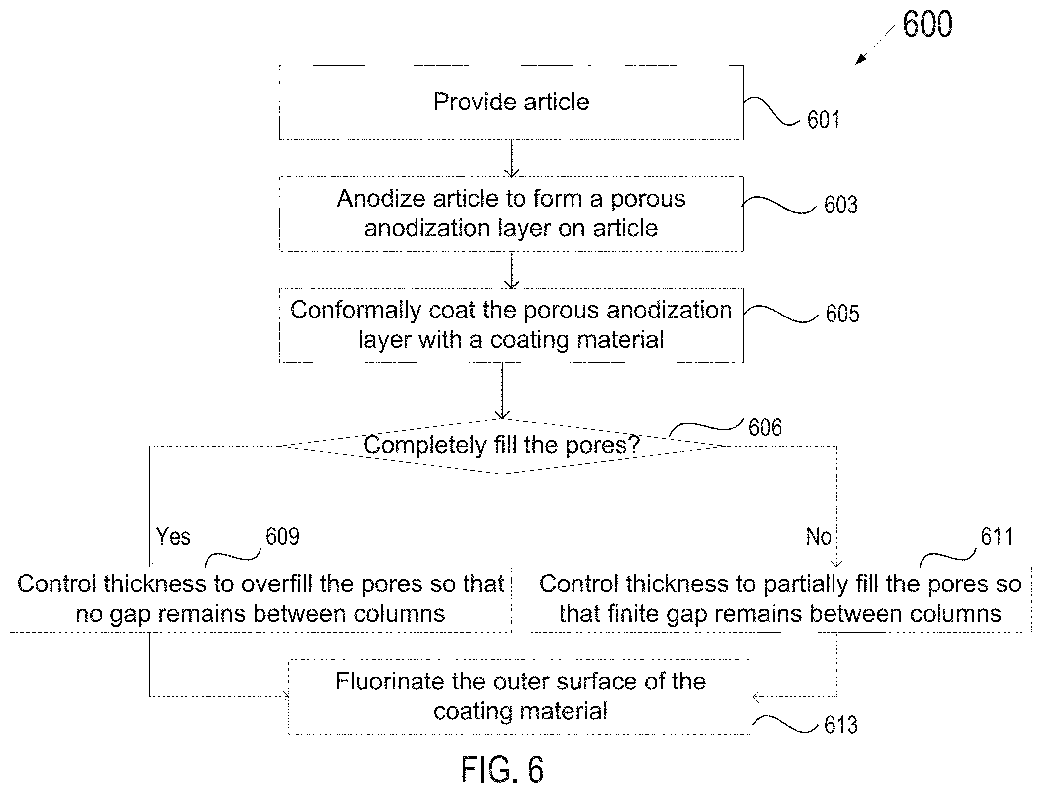
[0020] FIG. 6 is a flow chart showing a process for manufacturing an anodized article where the anodization layer is coated with one or more sealing layers of a coating material, in accordance with embodiments of the present disclosure.
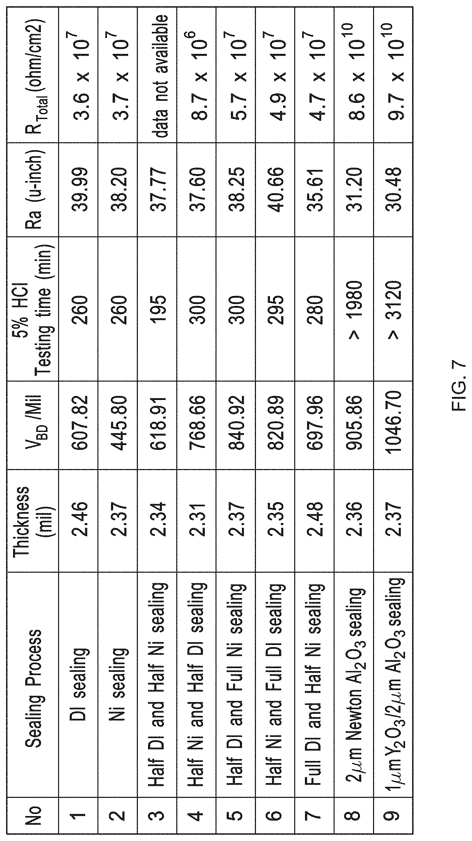
[0021] FIG. 7 shows a properties associated with various hybrid sealing and advanced coating and sealing processes in a tabular format, in accordance with embodiments of the present disclosure.
[0022] FIG. 8 illustrates impedance enhancement results corresponding to various hybrid sealing and advanced coating and sealing processes.
DETAILED DESCRIPTION OF EMBODIMENTS
[0023] Embodiments of the disclosure are directed to a process for anodizing an article (e.g., a component of a processing chamber for use in semiconductor manufacturing) to form a porous anodization layer and sealing the porous anodization layer fully or partially. Embodiments are additionally directed to an article created using an enhanced anodization and sealing process. For example, the article may be a showerhead, a heater, a cathode sleeve, a sleeve liner door, a cathode base, a chamber liner, an electrostatic chuck base, etc. of a chamber for processing equipment such as an etcher, a cleaner, a furnace, and so forth. For another example, the article may be a block-like chamber that contains the cylinder channel conducting the plasma flowing inside a plasma generation source, such as inside RPS. In one embodiment, the chamber is for a plasma etcher or plasma cleaner. In one embodiment, these articles can be formed of an aluminum alloy (e.g., Al 6061), another alloy, a metal, a metal oxide, or any other suitable material (e.g., a conductive material).
[0024] Due to impurities in the metals used to manufacture semiconductor chamber components (e.g., Al 6061), these components may not meet some semiconductor manufacturing specifications. For example, metal contamination specifications for device nodes having sizes of less than 90 nm may be stringent. These impurities can leach out of typical coated or anodized articles during plasma processing of a wafer and increase contamination levels. An anodization layer may have a porous outer layer comprising high aspect ratio columns. The porous layer may be sealed at the top. According to embodiments, parameters and/or techniques for anodization of these components (e.g., a thickness of an anodization layer) as well as for sealing a produced anodization layer may be optimized to reduce metal contamination from the article. Performance properties of the article may include a relatively long lifespan (as compared to other articles that have undergone a traditional anodization process and a traditional sealing process), and a low on-wafer metal contamination, according to embodiments.
[0025] Embodiments described herein may cause reduced on wafer metal contamination when used in a process chamber for plasma rich processes. However, it should be understood that the anodized and sealed articles discussed herein may also provide reduced metal contamination when used in process chambers for other processes such as non-plasma etchers, non-plasma cleaners, chemical vapor deposition (CVD) chambers, physical vapor deposition (PVD) chambers, selective removal process (SRP) chambers, and so forth.
[0026] Though anodization is used to maintain the process stability, the anodization surface often induces particles and metal contamination while the anodization parts are irradiated using fluorine or chlorine-containing plasma. Quality of anodization becomes worse with an increase in ion bombardment energy. The porous columnar portion of the anodized surface usually has some micro-cracks. Plasma erosion roughens the anodized surface and enlarges the cracks, shortening the anodized part's service life and introducing particle and metal contamination in the plasma process. The present disclosure improves the anodization process by creating a smooth and dense anodization surface with reduced micro-cracks. This improvement is enabled by modifying the anodization process with hybrid sealing and coating processes, leading to enhancing the plasma erosion resistance and reducing particle contamination.
[0027] FIG. 1A illustrates a cross-sectional view of a chamber component 100A for use in a manufacturing chamber (e.g., in a semiconductor manufacturing chamber), in accordance with one embodiment of the present disclosure. The chamber component 100 includes an article 102 and an anodization layer 103 on the article. The anodization layer 103 comprises a buffer layer 104 and a porous layer 106 comprising vertical columns 110 of the anodization layer material with pores 112 of diameter D in between the columns 110. The chamber component 100A is shown for representational purposes and is not necessarily to scale.
[0028] The article 102 may be manufactured of an aluminum alloy (e.g., 6061 Al). However, the article 102 can also be formed of any other suitable material, such as other metals or metal alloys. Examples of other suitable materials include, but are not limited to, stainless steel, titanium, titanium alloy, yttrium, yttrium alloy, magnesium, magnesium alloy etc. According to embodiments, the article 102 can be a showerhead, a cathode sleeve, a sleeve liner door, a cathode base, a chamber liner, an electrostatic chuck base, etc. of a chamber for processing equipment such as an etcher, a cleaner, a furnace, and so forth. According to embodiments, the article 102 can be the block with the cylinder channel conducting the plasma flowing inside the plasma generation source, such as inside the RPS.
[0029] The article 102 is anodized to form the anodization layer 103 on a surface of the article 102, where pores 112 are formed between anodization columns 110. The anodization layer may be an oxide, such as Al.sub.2O.sub.3, Y.sub.2O.sub.3, etc. For example, if the article 102 is aluminum or an aluminum alloy, then the anodization layer may be Al.sub.2O.sub.3. If the article 102 is yttrium or a yttrium alloy, then the anodization layer may be Y.sub.2O.sub.3. If the article is magnesium or a magnesium alloy, then the anodization layer may be MgO. The anodization layer 103 can be formed to have a certain thickness. In embodiments, the thickness of the anodization layer may be 0.2-75 um, and mostly 25-75.mu.m. In embodiments, the pores in the porous layer 106 of the anodization layer 103 have diameter D. Diameter D may be 10-100 nm, and mostly 15-80 nm. The thickness of the porous layer 106 and diameter D of the pores results in an aspect ratio of the anodization column 110 height to the pore diameter being in a range from about 10 to 1 (10:1) to about 2000 to 1 (2000:1) in embodiments. A typical height to width ratio for individual columns 110 may be greater than 300:1 in embodiments.
[0030] A post-anodization process is sealing the anodized layer by forming one or more sealing layer 114, 115 at the top of the porous layer 106, as shown in the modified (i.e. anodized and sealed) chamber component 100B in FIG. 1B. Sealing can be performed by using a combination of deionized water (DI) or steam, nickel plating (e.g., using nickel acetate), and/or application of polytetrafluoroethylene (PTFE), and/or or other sealing methods discussed below.
[0031] As shown, a multi-layer sealing layer comprising a first sealing layer 115 and a second sealing layer 114 is created in embodiments. The first sealing layer 115 may be nickel hydroxide if nickel acetate sealing is used, may be hydrated aluminum oxide (boehmit) if water or steam sealing is used, may be PTFE if application of PTFE is used, and so on. The second sealing layer 114 may likewise be nickel hydroxide if nickel acetate sealing is used, may be hydrated aluminum oxide (boehmit) if water or steam sealing is used, may be PTFE if application of PTFE is used, and so on. Other possible sealing techniques that may be used for the first and/or second sealing layers 114, 115 include sealing using nickel fluoride and sealing using potassium dichromate.
[0032] Different sealing techniques are used to produce the first sealing layer 115 and the second sealing layer 114. Accordingly, the multi-layer sealing layer includes layers of at least two different materials. Notably, the resultant sealing layer is a multi-layer (or hybrid) sealing layer that includes advantageous properties of two different types of sealants. For example, a hybrid sealing layer may combine the desirable properties of high breakdown voltage, designed surface smoothness and reduced surface defect density.
[0033] FIG. 1C shows that the sealing layer at the top of columns 110 may not be continuous as shown in FIG. 1B. Instead, in some embodiments, a first sealing layer 116 and a second sealing layer 117 may be formed at the top portions of each of the columns 110, narrowing the hollow space in pores 112 towards the top, but not completely closing the pores 112.
[0034] FIG. 2 illustrates an exemplary architecture of a manufacturing system 200 for manufacturing a chamber component (e.g., chamber component 100A of FIG. 1A). The manufacturing system 200 may be a system for manufacturing an article for use in semiconductor manufacturing. In one embodiment, the manufacturing system 200 includes processing equipment 201 connected to an equipment automation layer 215. The processing equipment 201 may include a block 203 that prepares a metallic article for anodization and sealing, an anodizer block 204 that forms an anodization layer, and a sealing block 205 that performs sealing on the anodization layer. The manufacturing system 200 may further include one or more computing devices 220 connected to the equipment automation layer 215. In alternative embodiments, the manufacturing system 200 may include more or fewer components. For example, the manufacturing system 200 may include manually operated (e.g., off-line) processing equipment 201 without the equipment automation layer 215 or the computing device 220.
[0035] The block 203 can adjust a surface roughness of an article prior to any layers or coatings being formed. For example, the block 203 may adjust a surface roughness of the article to be in a range from about 15 micro-inches to about 300 micro-inches (e.g., about 120 micro-inches). In other embodiments, the surface roughness of the article may be increased by grinding or bead blasting, or may be decreased by sanding or polishing. However, the surface roughness of the article may already be suitable, so surface roughness adjustment can be optional.
[0036] In one embodiment, anodizer 204 is a system configured to form an anodization layer on the metallic article. For example, the article (e.g., a conductive article) may be immersed in an anodization bath, e.g., including sulfuric acid, oxalic acid, phosphoric acid, or a mixture of these acids. An electrical current is applied to the article such that the article becomes an anode. The anodization layer then forms on the metallic article.
[0037] In one embodiment, after anodization, the article can be baked in a heating apparatus (e.g., an oven) for certain period (e.g., 2 hours to 12 hours) at a certain temperature (e.g., 60 degrees C. to 150 degrees C.) to remove residual moisture from the article and/or the anodization layer.
[0038] The block 205 is a system configured to seal the anodized surface, according to the various methods described below. Block 205 may be an atomic layer deposition (ALD) system, a physical vapor deposition (PVD) system, a chemical vapor deposition (CVD) system, a plasma enhanced chemical vapor deposition (PECVD) system, a plasma enhanced physical vapor deposition (PEPVD) system, or a wet chemical deposition system (such as a sol gel system or a slurry printing system). For DI sealing, block 205 may include a steam generator. For nickel sealing, block 205 may include a plating bath containing nickel acetate solution. For PTFE sealing, block 205 may include a system for spraying, dipping or brushing a PTFE-containing thermosetting resin.
[0039] The equipment automation layer 215 may interconnect some or all of the manufacturing machines 201 with computing devices 220, with other manufacturing machines, with metrology tools and/or other devices. The equipment automation layer 215 may include a network (e.g., a location area network (LAN)), routers, gateways, servers, data stores, and so on. Manufacturing machines 201 may connect to the equipment automation layer 215 via a SEMI Equipment Communications Standard/Generic Equipment Model (SECS/GEM) interface, via an Ethernet interface, and/or via other interfaces. In one embodiment, the equipment automation layer 215 enables process data (e.g., data collected by manufacturing machines 201 during a process run) to be stored in a data store (not shown). In an alternative embodiment, the computing device 220 connects directly to one or more of the manufacturing machines 201.
[0040] In one embodiment, some or all manufacturing machines 201 include a programmable controller that can load, store and execute process recipes. The programmable controller may control temperature settings, gas and/or vacuum settings, time settings, etc. of manufacturing machines 201. The programmable controller may include a main memory (e.g., read-only memory (ROM), flash memory, dynamic random access memory (DRAM), static random access memory (SRAM), etc.), and/or a secondary memory (e.g., a data storage device such as a disk drive). The main memory and/or secondary memory may store instructions for performing heat treatment processes described herein.
[0041] The programmable controller may also include a processing device coupled to the main memory and/or secondary memory (e.g., via a bus) to execute the instructions. The processing device may be a general-purpose processing device such as a microprocessor, central processing unit, or the like. The processing device may also be a special-purpose processing device such as an application specific integrated circuit (ASIC), a field programmable gate array (FPGA), a digital signal processor (DSP), network processor, or the like. In one embodiment, programmable controller is a programmable logic controller (PLC).
[0042] The parameters of the various possible sealing processes are now discussed in greater detail.
[0043] One of the possible sealing techniques is sealing the anodization layer with DI water at high temperature, the technique being known as DI sealing (or DI water sealing, or DI steam sealing). In DI sealing, an anodized part is immersed into deionized water (e.g., hot DI water at about 96-100.degree. C.) or steam to form hydrated aluminum oxide (boehmit) in columnar pores of the anodization layer. The hydrated aluminum oxide swells the columns at least near a surface of the porous layer of the anodization layer, reducing a surface porosity of the porous layer. For example, the sealing layer 114 or sealing layer 115 in FIG. 1B may be a hydrated aluminum oxide layer. DI sealing is performed to close or seal the columnar structure (e.g., the pores) of the anodization layer. The sealing layer 114 may be formed at the top, leaving some hollow space 112 underneath the sealing layer.
[0044] Without a high quality sealing, the anodization layer may be highly absorbent of dirt, grease, oils and stains. Typically, DI sealing is performed to give high corrosion resistance. Typically, DI water sealing rate is about 2 to 3 minutes per micrometer of oxide coating. Therefore, for a hard anodization (e.g., HA (III)) with 2 to 2.5 mils thickness of the anodization layer, the water sealing time would be around 1.0 hour to 4.0 hours. The time variation is highly dependent on the temperature of the water or steam. A higher temperature is correlated to faster sealing. To maintain a uniform temperature throughout the entire tank used to perform the DI water or steam sealing, a small amount of air agitation may be used. The pH of the solution is in the range of 5.5-6.5 and may be adjusted with ammonia and/or other agents for an optimal seal. DI water sealing quality is usually controlled by the control of pH value and the sealing temperature. By clogging up the pores on the surface, the anodized aluminum sealed with DI water has the advantages of stronger structural integrity, enhanced dielectric strength, high purity semiconductor processing, etc. For example, for a 62.5 .mu.m (2.5 mil) thickness of anodization layer on aluminum, post DI water sealing, the roughness is less than less than 0.8 .mu.m (32 .mu.-inch), 5% HCl corrosion time (a measure of structural integrity) is 2.5-3.0 hours, and dielectric strength is 30-32V/.mu.m (750-800 V/mil).
[0045] An alternative to DI sealing is post-anodization nickel plating for sealing the anodization layer. Ni sealing, also called nickel acetate sealing, comprises immersing the anodized aluminum in a boiling nickel acetate solution. Hydrolysis occurs, which causes nickel hydroxide to precipitate into the pores of the porous layer of the anodization layer. As a result of the nickel acetate sealing, nickel ions (e.g., nickel hydroxide) are incorporated into the pores of the porous layer. The nickel ions (e.g., nickel hydroxide) then block or fill the mouths of these pores.
[0046] Ni sealing may be performed at a temperature of 93-99.degree. C. (200-210.degree. F.). The sealing time can be adjusted. For example, in a range of 10-80 minutes for hard anodized (e.g., HA (III)) parts that have 2 mils or 2.5 mils (50 .mu.m to 62.5 .mu.m) thick anodization structure, the sealing time is in the range of 10-80 minutes, which is equal to 2-3 minutes per 0.10 mil (approximately 2.5 .mu.m) of oxide coating thickness. The chemical formulation of the Ni sealing solution may comprise nickel acetate in the range of 4-5 g/l, some specialty dispersant in the range of 2-3 g/l, benzoic acid in the range of 1-2 g/l and high purity DI water. The pH value of the Ni sealing solution is in the range of 5-7, which can be adjusted by adding diluted ammonium hydroxide. However, the sealing quality is usually controlled by controlling the nickel acetate concentration and the sealing temperature. Before sealing, a thorough rinse is recommended to remove any foreign substances. The article should be thoroughly rinsed immediately after nickel plating before it is dried. Ni sealing can make the smooth anodization surface with superior acid resistance. For example, for a 62.5 .mu.m (2.5 mil) thickness of anodization layer on aluminum, post Ni acetate sealing, 5% HCl corrosion time (a measure of structural integrity) is 2.5-3.0 hours. The roughness is less than less than 0.8 um (32 .mu.-inch), i.e. comparable to DI water sealing. But the dielectric strength is 20-22V/.mu.m (500-550 V/mil), i.e. less than what is achievable by DI water sealing.
[0047] Another technique for Ni sealing is performed using nickel fluoride. This process is a cold sealing process that may be used as an alternative to hot sealing methods. For Ni sealing using nickel fluoride, fluoride nickel is introduced to the anodized aluminum. The fluoride ions enter into the pores, which act as the place for an exchange mechanism. Once in the pores, the fluoride ions cause a shift in pH, which causes nickel ions to precipitate. Nickel hydroxide is then formed, which blocks the mouth of the pores, effectively sealing the porous layer. Water from the atmosphere may then diffuse into the nickel hydroxide, causing the pores to become effectively blocked.
[0048] When used in the plasma generator chamber, the anodized Al surface sealed by DI water or Ni acetate reacts with fluorine-containing plasma (e.g., NF3 generated plasma), forming AlF3 deposition on the anodized surface and then induces AlF3 or AlF0-based particle contamination after some length of service time. For example, chamber particle count may reach more than 100, compared to the desired particle control specification (<15 particles at size <26 nm on wafer), when service time exceeds 100RF hours. This unstable anodization surface adversely impacts the chamber process performance and reduces production yield.
[0049] A third sealing process is PTFE (commercially known as teflon) sealing. PTFE sealing comprises spraying, dipping, or brushing a thermosetting resin containing PTFE to the unsealed surface of the porous layer of the anodization layer (anodized surface). The article can then be cured at 165-185.degree. C. for around 1 hour, to form a PTFE-film-sealed anodization surface. The sealed PTFE thickness depends on the desired use of the anodized sealed article. Thicker PTFE coating can be achieved by a multi-cycle sealing process. Teflon sealing forms an anodized sealed surface with high smoothness, high dielectric strength and strong acid resistance. However, a disadvantage is that the surface of the PTFE coating is relatively soft and easy to be damaged by any mechanical friction during handling and/or assembly.
[0050] Depending on the sealing process time and temperature, the electrical current, and sealing materials, the resultant anodization surface could be rough or smooth, and may have some structural cracks around the corners of the metallic article and/or abnormality at other geometric locations. The surface roughness and defect density directly affect the measurable properties of the anodization layer, such as the dielectric strength (indicated by breakdown voltage, V.sub.bd) and acid solution resistance of the anodized surface. Acid solution resistance is measured by 5% HCl bubble testing for various durations. The variation on the V.sub.bd and the bubble test time can indicate the durability of the anodization layer in the plasma environment. For instance, a DI water steam sealed cellular Al.sub.2O.sub.3 anodization layer exhibits high dielectric strength but rough surface finish with increased numbers of micro-cracks. This leads to a short bubble test time and possibly increases particle contamination risk during later processing in plasma rich environments. In contrast, a Ni plating sealed cellular Al.sub.2O.sub.3 layer demonstrates a very smooth and dense anodized surface, but relatively low dielectric strength. This may cause the anodized surface to be easily eroded by plasma through physical bombardment (as V.sub.bd is low) and may induce metal contamination. A dense and smooth anodized surface can be achieved using the PTFE sealing process. However, the resulting anodized surface after PTFE sealing is soft and easily damaged during handling, processing and assembling.
[0051] With the selection and the combination of different sealing processes and different orders of those sealing processes, the anodized and sealed surface can be designed to have desired surface smoothness, reduced surface defect density and increased dielectric strength.
[0052] In one embodiment, DI water steam sealing and Ni sealing are combined to seal the anodization layer without reducing anodization layer thickness. The sealed anodization layer comprising a multi-layer seal maintains high dielectric strength and high hardness compared to when only DI water sealing is used. At the same time, smoothness of the surface improves compared to when only DI water sealing is used. Order of DI water sealing and Ni sealing may be interchanged. In one embodiment, DI water/steam sealing is performed first, followed by Ni sealing. Alternatively, Ni sealing is performed first, followed by DI water/steam sealing. Depending on the plasma environment conditions, the final sealing process may be chosen to be either Ni plating or DI water steam sealing, depending on whether surface smoothness or dielectric strength of the outermost layer is more desirable. In addition, the properties such as the dielectric strength and the final surface smoothness of the anodized structure can be tailored by adjusting process time, temperature and other conditions in each sealing process.
[0053] In one embodiment, a dense and smooth anodization with high dielectric strength can be achieved by the anodization followed by hybridization of DI water steam sealing and the PTFE sealing processes. In one embodiment, DI water/steam sealing is performed first, followed by PTFE sealing. Alternatively, PTFE sealing is performed first, followed by DI water/steam sealing. Compared to Ni plating, both water steam sealing and the PTFE sealing help to increase dielectric strength because of the improved dense and smooth surface. By preventing dielectric breakdown of the process chamber components, a stable plasma can be maintained during the plasma process, improving semiconductor wafer yield.
[0054] In one embodiment, Ni sealing is performed first, followed by PTFE sealing. Alternatively, PTFE sealing is performed first, followed by Ni sealing.
[0055] This disclosure encompasses any permutation or combination of the above three sealing processes, i.e. DI sealing, Ni sealing and PTFE sealing, to form a hybrid multi-layer sealing layer that results in an enhanced anodized surface for processing chamber components.
[0056] In an alternative implementation, a hybrid sealing process may involve deposition of a coating material and/or surface alloying to cover and protect the anodized surface after performing one or more of DI sealing, Ni sealing and/or PTFE sealing. Alternatively, sealing may be performed by depositing a conformal layer over the pores of the porous layer of the anodization layer. The coating material may be referred to as an "advanced coating" material. The coating material may be an oxide, an oxy-fluoride or a fluoride. Possible examples include, but are not limited to, Al.sub.2O.sub.3, AlF.sub.3, Y.sub.2O.sub.3, Y--O--F (e.g., Y.sub.5O.sub.4F.sub.7), Er.sub.2O.sub.3, YF.sub.3, Y.sub.3Al.sub.5O.sub.12 (YAG), Er.sub.3Al.sub.5O.sub.12 (EAG), Y.sub.4Al.sub.2O.sub.9 (YAM), YAlO.sub.3 (YAP), Er.sub.4Al.sub.2O.sub.9 (EAM), ErAlO.sub.3 (EAP), a solid solution of Y.sub.2O.sub.3--ZrO.sub.2, a ceramic compound comprising Y.sub.4Al.sub.2O.sub.9 and a solid-solution of Y.sub.2O.sub.3--ZrO.sub.2, and their combinations.
[0057] With reference to the solid-solution of Y.sub.2O.sub.3--ZrO.sub.2, the coating material may include Y.sub.2O.sub.3 at a concentration of 10-90 molar ratio (mol %) and ZrO.sub.2 at a concentration of 10-90 mol %. In some examples, the solid-solution of Y.sub.2O.sub.3--ZrO.sub.2 may include 10-20 mol % Y.sub.2O.sub.3 and 80-90 mol % ZrO.sub.2, may include 20-30 mol % Y.sub.2O.sub.3 and 70-80 mol % ZrO.sub.2, may include 30-40 mol % Y.sub.2O.sub.3 and 60-70 mol % ZrO.sub.2, may include 40-50 mol % Y.sub.2O.sub.3 and 50-60 mol % ZrO.sub.2, may include 60-70 mol % Y.sub.2O.sub.3 and 30-40 mol % ZrO.sub.2, may include 70-80 mol % Y.sub.2O.sub.3 and 20-30 mol % ZrO.sub.2, may include 80-90 mol % Y.sub.2O.sub.3 and 10-20 mol % ZrO.sub.2, and so on.
[0058] With reference to the ceramic compound comprising Y.sub.4Al.sub.2O.sub.9 and a solid-solution of Y.sub.2O.sub.3--ZrO.sub.2, in one embodiment the ceramic compound includes 62.93 molar ratio (mol %) Y.sub.2O.sub.3, 23.23 mol % ZrO.sub.2 and 13.94 mol % Al.sub.2O.sub.3. In another embodiment, the ceramic compound can include Y.sub.2O.sub.3 in a range of 50-75 mol %, ZrO.sub.2 in a range of 10-30 mol % and Al.sub.2O.sub.3 in a range of 10-30 mol %. In another embodiment, the ceramic compound can include Y.sub.2O.sub.3 in a range of 40-100 mol %, ZrO.sub.2 in a range of 0.1-60 mol % and Al.sub.2O.sub.3 in a range of 0.1-10 mol %. In another embodiment, the ceramic compound can include Y.sub.2O.sub.3 in a range of 40-60 mol %, ZrO.sub.2 in a range of 35-50 mol % and Al.sub.2O.sub.3 in a range of 10-20 mol %. In another embodiment, the ceramic compound can include Y.sub.2O.sub.3 in a range of 40-50 mol %, ZrO.sub.2 in a range of 20-40 mol % and Al.sub.2O.sub.3 in a range of 20-40 mol %. In another embodiment, the ceramic compound can include Y.sub.2O.sub.3 in a range of 80-90 mol %, ZrO.sub.2 in a range of 0.1-20 mol % and Al.sub.2O.sub.3 in a range of 10-20 mol %. In another embodiment, the ceramic compound can include Y.sub.2O.sub.3 in a range of 60-80 mol %, ZrO.sub.2 in a range of 0.1-10 mol % and Al.sub.2O.sub.3 in a range of 20-40 mol %. In another embodiment, the ceramic compound can include Y.sub.2O.sub.3 in a range of 40-60 mol %, ZrO.sub.2 in a range of 0.1-20 mol % and Al.sub.2O.sub.3 in a range of 30-40 mol %. In other embodiments, other distributions may also be used for the ceramic compound.
[0059] Any of the aforementioned ceramic coatings may include trace amounts of other materials such as ZrO.sub.2, Al.sub.2O.sub.3, SiO.sub.2, B.sub.2O.sub.3, Er.sub.2O.sub.3, Nd.sub.2O.sub.3, Nb.sub.2O.sub.5, CeO.sub.2, Sm.sub.2O.sub.3, Yb.sub.2O.sub.3, or other oxides.
[0060] A conventional sealing process may be replaced by the non-line-of-sight deposition of one of the aforementioned coating materials directly onto the un-sealed anodization layer, to seal the anodized porous columnar structure. The coating material ideally should have thermal expansion coefficient close to the underlying anodization layer to reduce the possibility of thermally induced stress. The advanced coating material should also have high stability against plasma erosion, and ideally would not generate deposition by-products (such as AlF.sub.3, AlOF, etc. in fluorine and/or chlorine-containing plasma environments).
[0061] The sealing layer should be formed using deposition processes that allow conformal coverage onto the anodization layer columns, i.e. there should be uniform and controllable thickness even within the pores between the columns. One example approach is the deposition of one or more layers of coating material using atomic layer deposition process (ALD).
[0062] ALD is one of the suitable methods for forming a multi-component coating composition on a chamber component for a processing chamber. The method may include depositing a first film layer (e.g., an oxide or a fluoride) onto a surface of a chamber component. The first film layer is grown from at least two precursors. The method further includes depositing a second film layer of an additional oxide or an additional fluoride onto the surface of the chamber component. The second film layer may be grown from at least two additional precursors using the atomic layer deposition process. In some embodiments, additional layers may be deposited too.
[0063] The various components may be arranged in different layers of the multi-component coating. In some embodiments, after processing (such as annealing) the multiple layers of the multi-component coating may interdiffuse to form a homogenous or approximately homogenous coating that includes the constituent materials of the different layers. For example, the multiple components from the different layers may form a solid state phase of a first film layer and a second film layer.
[0064] Persons skilled in the art would appreciate that ALD is merely an example process for coating deposition and does not limit the scope of the disclosure. Other processes, such as physical vapor deposition (PVD), chemical vapor deposition (CVD), plasma enhanced chemical vapor deposition (PECVD), plasma enhanced physical vapor deposition (PEPVD), and wet chemical depositions (sol gel, slurry printing, etc.) may be used too.
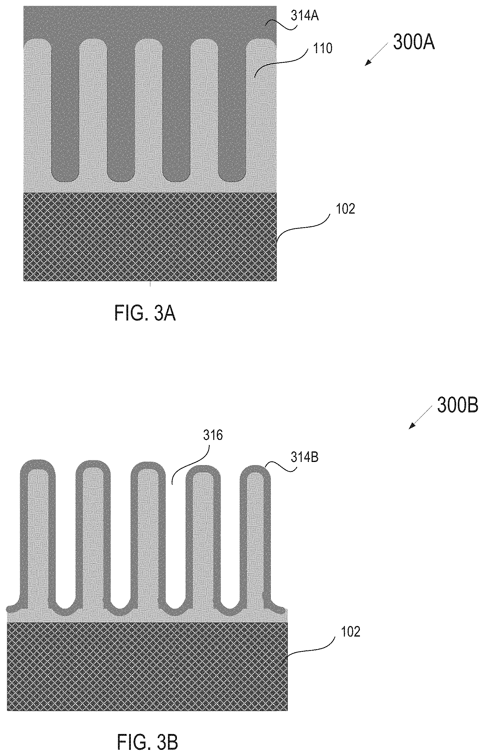
[0065] In one embodiment, thickness of the advanced coating is controlled, so that the pores are fully filled between the columns 110. FIG. 3A shows an advanced coating layer 314A (comprising one or more layers of a single material, or more than one layers of more than one material) that overfills the pores and builds additional thickness at the top of the columns 110 of the anodization layer 103. The pores have diameters in the range of 25-60 nm in embodiments. The advanced coating results in a dense and pore-free solid structure 300A, which can be either crystalline or amorphous.
[0066] In another embodiment, thickness of the advanced coating is controlled, so that the pores are partially filled between the columns 110, as shown in FIG. 3B. In this embodiment, the advanced coating layer 314B conformally covers the columns, leaving a pore gap 316 between the columns. The pore size may be reduced to the range of 5-60 nm due to the additional thickness of the advanced coating layer 314B onto the columns 110. This is known as an open column structure. One of the advantages of an open column structure 300B is that it can adapt to temperature variation better than a solidly sealed structure 300A shown in FIG. 3A or a hybridly sealed structure 100B shown in FIG. 1B. Specifically, the gap between the coated columns of the porous layer of the anodization layer leaves space for the columns to expand without introducing additional stress to the anodization layer.
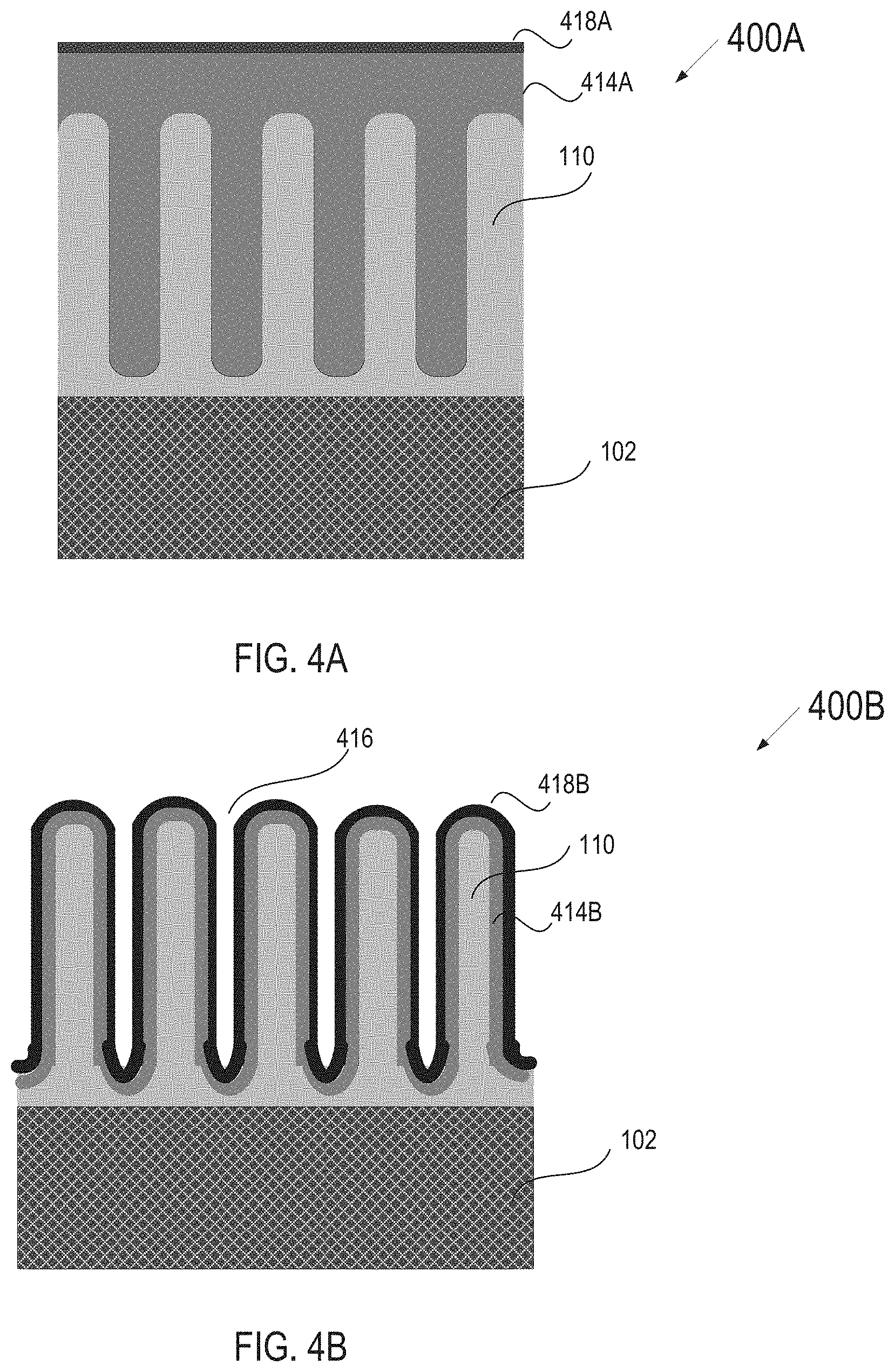
[0067] As described above, the anodization layer columns sealed with one or more layers of advanced coating materials greatly reduce plasma erosion and undesired by-product formation during plasma processes. In order further to reduce the risk of the process drift induced by the formation of by-products, such as AlF3 from an Al2O3 coating, or YF3/YOF from the Y2O3 coating, in one embodiment, the present disclosure describes in-situ fluorination over the advanced coating surface. Fluorination can be conducted through a wet chemical reaction process, a relative high-temperature heating process in the presence of fluorine, and/or an in-situ plasma irradiation process using a fluorine-containing plasma in a plasma processing chamber. The fluorination process creates a dense and smooth surface of a metal fluoride or a metal oxyfluoride (e.g., with YF3, YOF, AlF3, AlOF, etc.), depending on the plasma process chemistry and the composition of the underlying advanced coating material. For example, Y2O3 converts to YxOyFz or YF3, a solid solution of Y2O3-ZrO2 converts to Y--Zr--O--F (e.g., YaZrbOcFd) or YxZyFz, and so on. In general, when the advanced coating material has an oxide layer, conducting in-situ fluorination replaces at least a portion of oxygen molecules of the oxide with fluorine molecules and converts at least a surface of the coating from the oxide into a fluoride or an oxy-fluoride.
[0068] In an example implementation of a first method for forming a Y--O--F layer or coating, a yttrium-containing coating (e.g., a Y2O3 coating or Y2O3-ZrO2 solid solution coating) is deposited on a surface of a chamber component for a first processing chamber. Alternatively a MxOy coating may be deposited, where M is a metal such as Al or a rare earth metal. The chamber component is heated to an elevated temperature of about 150-1000.degree. C. (e.g., 150-500.degree. C.). The chamber component is exposed to a fluorine source such as HF, NF3, NF3 plasma, F2, F radicals, etc. at the elevated temperature for a duration of time. As a result, at least a surface of the yttrium-containing oxide coating is converted into a Y--O--F layer or other yttrium-based oxy-fluoride layer or coating. In some instances, an entirety of the yttrium-containing oxide coating is converted to Y--O--F or other yttrium containing oxy-fluoride. Alternatively, at least a surface of the MxOy coating is converted to a M-O--F layer.
[0069] In an example implementation of a second method for forming a Y--O--F layer or coating, atomic layer deposition (ALD), chemical vapor deposition (CVD), ion assisted deposition (IAD) or any other suitable method is performed to deposit a YF3 coating having a thickness of about 10 nm to about 10 microns onto a surface of a chamber component for a processing chamber. The chamber component is heated to an elevated temperature of about 150-1500.degree. C. The chamber component is exposed to an oxygen source at the elevated temperature for a duration of about 12-24 hours. As a result, the YF3 coating is converted into a Y--O--F coating.
[0070] In an example implementation of a third method for forming a M-O--F layer or coating, a substrate is loaded into a processing chamber, the processing chamber comprising one or more chamber components that include a metal oxide coating. A fluorine-based plasma from a remote plasma source is introduced into the processing chamber. The metal oxide coating is reacted with the fluorine-based plasma to form a temporary M-O--F layer or metal fluoride layer over the metal oxide coating. A process that utilizes a corrosive gas is then performed on the substrate. The process removes or adds to the temporary M-O--F layer or metal fluoride layer, but the temporary M-O--F layer or metal fluoride layer protects the metal oxide coating from the corrosive gas.
[0071] FIG. 4A shows a pore-free structure 400A where a fluorinated outer surface layer 418A is formed on the advanced coating layer 414A that seals the anodization layer columns 110 by completely filling up the pores (as in FIG. 3A). FIG. 4B shows an open structure 400B where a fluorinated outer surface layer 418B is formed on the advanced coating layer 414B that seals the anodization layer columns 110 by partially filling up the pores (as in FIG. 3B), still leaving a gap 416 between the columns 110, but with altered diameter of the pore due to the addition of the fluorinated layer 418B. Persons skilled in the art will appreciate that since there is chemical reaction involved in fluorination that changes surface characteristics of the advanced coating layer underneath, the pore size alternation may reduce the pore size (for example, conversion from Y2O3 to Y--O--F or YF3 may cause a volume expansion and reduce the pore size), but that is not always the case. As in case of the open structure 300B, the open structure 400B also have advantageous thermal properties, because the pores help in adapt to temperature variation without causing significant thermal stress in the sealed structure. Further to enhance the anodization surface performance, in some embodiments, the sealed anodized components may be heated or annealed to stabilize the coating or coated structure.
[0072] The advanced coating protected anodized structure may slow down plasma erosion and reduce the metal and particle contamination of an article due to the smooth and defect-free surface. This improves the plasma process stability and durability. The advanced coating sealed anodized articles with or without surface fluorination can also be used in processing chambers that perform PVD, CVD and/or plasma etching processes.
[0073] Surface fluorination through acid immersion may be performed using mixed acid solutions containing HF, NH4F, and H2O2 in predetermined volumetric ratio based on the underlying coating layer properties (e.g., what coating material is used, how many layers are used, what thickness is used etc.) and the desired properties of the fluorinated outer surface (e.g., porosity area, fluorinated layer thickness etc.). Using the methods of sealing disclosed here, the size of the pores post-coating can be adjusted in the range of 5-60 nm, depending on the actual application in different chamber systems and chamber processes used. This range of pore size can be achieved either post-fluorination or pre-fluorination.
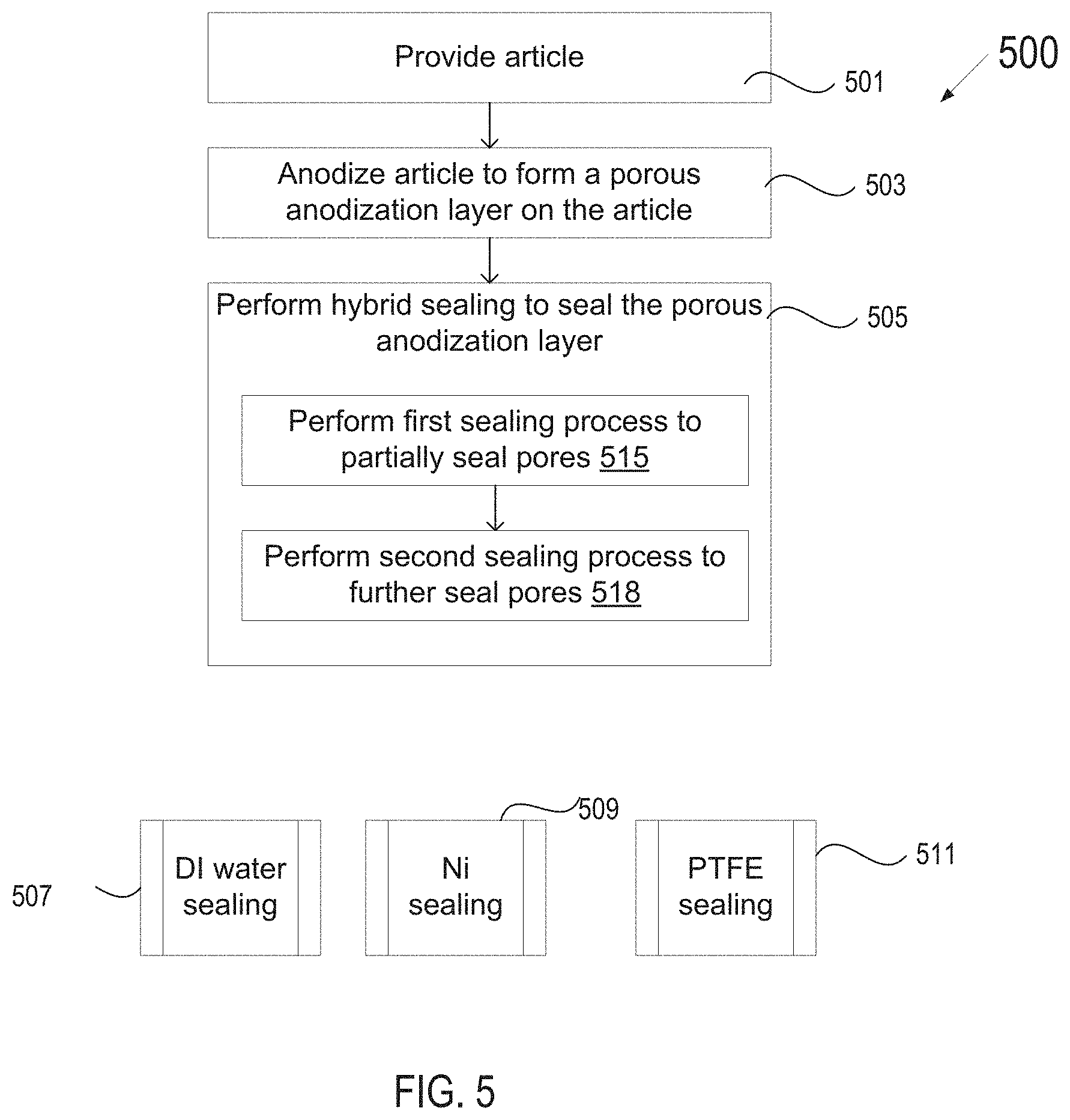
[0074] FIG. 5 is a flowchart showing a method 500 for manufacturing an anodized sealed article, in accordance with embodiments of the present disclosure. The operations of method 500 may be performed by various manufacturing machines, as set forth in FIG. 2.
[0075] At block 501, an article is provided. For example, the article can be a conductive article formed of an aluminum alloy (e.g., Al 6061) or another metallic article or article that contains a metallic part. The article can be a shower head, a cathode sleeve, a sleeve liner door, a cathode base, a chamber liner, an electrostatic chuck base, etc., for use in a processing chamber. Though not shown specifically, the article may be cleaned and its roughness may be altered in order to prepare the article for subsequent anodization.
[0076] At block 503, the article is anodized to form an anodization layer (e.g., formed of Al.sub.2O3), according to one embodiment. The anodization layer has a porous layer at the top, as discussed above. In one embodiment, the article can be baked after anodization, as described above, to remove residual moisture from pores of the anodization layer.
[0077] At block 505, a hybrid sealing layer is formed at the top of the porous layer by performing a hybrid sealing process. The hybrid sealing process comprises performing a first sealing process at block 515 to partially seal the pores of a porous layer of an anodization layer and performing a second sealing process at block 518 to further seal the pores of the porous layer. The first sealing process and the second sealing process each comprise one of DI water sealing (block 507), Ni sealing (block 509), and PTFE sealing (block 511). These three sealing processes may be performed in any order to produce target plasma resistant properties and/or other properties of the sealed anodized article.
[0078] FIG. 6 is a flowchart showing an alternative method 600 for manufacturing an anodized sealed article, in accordance with embodiments of the present disclosure. The operations of method 600 may be performed by various manufacturing machines, as set forth in FIG. 2.
[0079] Blocks 601 and 603 are similar to blocks 501 and 503 in flowchart 500. In block 605, the porous anodization layer is coated with a coating material. If multiple layers of coating are desired, then the operation of block 605 may be repeated until all layers are deposited. Multiple layers of the same coating material or multiple layers of different coating materials may be deposited in block 605. The operation of block 605 may be coextensive with the operation of decision block 607. If it is desired to completely fill the pores, then the thickness is controlled (block 609) so that no gap remains between columns, and optionally additional thickness is built at the top of the columns. The thickness may be controlled by repeating the operations of block 605 and depositing additional layers of the coating material (or materials) until a target thickness is reached. If it is desired to partially fill the pores to result in an open structure (as shown in FIGS. 3B and 4B), then the thickness is controlled (block 611) so that a finite gap remains between columns. The thickness may be controlled by repeating the operations of block 605 and depositing additional layers of the coating material (or materials) until a target thickness is reached.
[0080] Finally, an optional in-situ fluorination process may be added (block 613) to fluorinate the outer surface of the coating material used to seal the porous anodization layer.
[0081] In one embodiment, prior to performing the operations of block 605, one or more of DI sealing, Ni sealing or PTFE sealing are performed.
[0082] The resulting anodized sealed article produced by the methods of flowcharts 500 and 600 demonstrate superior resistance against plasma erosion. Therefore, less contaminants are introduced in the wafers during processing, as well as the service life of the article is prolonged.
[0083] FIG. 7 shows a properties associated with various hybrid sealing and advanced coating and sealing processes in a tabular format, in accordance with embodiments of the present disclosure. Persons skilled in the art would appreciate that these processes are merely examples processes encompassed by this disclosure, while many other processes are within the scope of this disclosure. The specific processes shown in the table are: a first process comprising DI-only sealing (row 1), a second process comprising Ni-only sealing (row 2), a third process (hybrid sealing process) comprising DI sealing for half the regular time period of DI-only sealing followed by Ni sealing for half the regular time period of Ni-only sealing (row 3), a fourth process (another hybrid sealing process) comprising Ni sealing for half the regular time period of Ni-only sealing followed by DI sealing for half the regular time period of DI-only sealing (row 4), a fifth process (yet another hybrid sealing process) comprising DI sealing for half the regular time period of DI-only sealing followed by Ni sealing for the entire regular time period of Ni-only sealing (row 5), a sixth process (yet another hybrid sealing process) comprising Ni sealing for half the regular time period of Ni-only sealing followed by DI sealing for the entire regular time period of DI-only sealing (row 6), a seventh process (yet another hybrid sealing process) comprising DI sealing for the entire regular time period of DI-only sealing followed by Ni sealing for half of the regular time period of Ni-only sealing (row 7), an eighth process using an advanced Al.sub.2O.sub.3 coating to enhance the sealing function (row 8), and a ninth process using an advanced Y.sub.2O.sub.3/Al.sub.2O.sub.3 coating to enhance the sealing function (row 9).
[0084] Combination of Ni and DI water sealing improves the sealing by increasing the breakdown voltage (V.sub.bd), and resistance to acids (e.g., HCl acid), as well as increases electrical resistance. The surface roughness R.sub.a and total resistivity R are tabulated in the last two columns corresponding to each process. It is noted that advanced newton single or double coatings enhances the smoothness of the anodized surface while enhancing the breakdown voltage, acid resistance and electrical resistance.
[0085] FIG. 8 illustrates impedance enhancement results corresponding to various hybrid sealing and advanced coating and sealing processes. The plots in FIG. 8 show potentiostatic electrochemical impedance spectroscopy (EIS) results for articles that have been coated and sealed according to various processes disclosed herein. Specifically, the y-axis is the impedance (Z.sub.mod) for an area and the x-axis is the frequency in Hz. As shown, bare Al has the lowest impedance value. Al with an anodization layer has impedance values that are generally acceptable. The hybrid sealing comprising DI water sealing and Ni plating sealing slightly increases the impedance of the formed anodization layer, though it has been observed that at temperature beyond 120.degree. C. (e.g., at 150.degree. C.), anodization layer impedance drops. Advanced single coating (e.g., 2 .mu.m Al.sub.2O.sub.3) or advanced double coating (e.g., 1 .mu.m Y.sub.2O.sub.3/2 .mu.m Al.sub.2O.sub.3)-based sealing greatly increases the impedance even at much higher temperature than 120.degree. C. (e.g., in the range of 350.degree. C.), and the coating remains stable.
[0086] The preceding description sets forth numerous specific details such as examples of specific systems, components, methods, and so forth, in order to provide a good understanding of several embodiments of the present disclosure. It will be apparent to one skilled in the art, however, that at least some embodiments of the present disclosure may be practiced without these specific details. In other instances, well-known components or methods are not described in detail or are presented in simple block diagram format in order to avoid unnecessarily obscuring the present disclosure. Thus, the specific details set forth are merely exemplary. Particular implementations may vary from these exemplary details and still be contemplated to be within the scope of the present disclosure.
[0087] Reference throughout this specification to "one embodiment" or "an embodiment" means that a particular feature, structure, or characteristic described in connection with the embodiment is included in at least one embodiment. Thus, the appearances of the phrase "in one embodiment" or "in an embodiment" in various places throughout this specification are not necessarily all referring to the same embodiment. In addition, the term "or" is intended to mean an inclusive "or" rather than an exclusive "or."
[0088] Although the operations of the methods herein are shown and described in a particular order, the order of the operations of each method may be altered so that certain operations may be performed in an inverse order or so that certain operation may be performed, at least in part, concurrently with other operations. In another embodiment, instructions or sub-operations of distinct operations may be in an intermittent and/or alternating manner.
[0089] It is to be understood that the above description is intended to be illustrative, and not restrictive. Many other embodiments will be apparent to those of skill in the art upon reading and understanding the above description. The scope of the disclosure should, therefore, be determined with reference to the appended claims, along with the full scope of equivalents to which such claims are entitled.
* * * * *
D00000
D00001
D00002
D00003
D00004
D00005
D00006
D00007
D00008
XML
uspto.report is an independent third-party trademark research tool that is not affiliated, endorsed, or sponsored by the United States Patent and Trademark Office (USPTO) or any other governmental organization. The information provided by uspto.report is based on publicly available data at the time of writing and is intended for informational purposes only.
While we strive to provide accurate and up-to-date information, we do not guarantee the accuracy, completeness, reliability, or suitability of the information displayed on this site. The use of this site is at your own risk. Any reliance you place on such information is therefore strictly at your own risk.
All official trademark data, including owner information, should be verified by visiting the official USPTO website at www.uspto.gov. This site is not intended to replace professional legal advice and should not be used as a substitute for consulting with a legal professional who is knowledgeable about trademark law.