Power Module For Supporting High Current Densities
Henning; Jason Patrick ; et al.
U.S. patent application number 16/171521 was filed with the patent office on 2019-02-28 for power module for supporting high current densities. The applicant listed for this patent is Cree, Inc.. Invention is credited to Anant Kumar Agarwal, Scott Allen, Jason Patrick Henning, John Williams Palmour, Sei-Hyung Ryu, Qingchun Zhang.
| Application Number | 20190067468 16/171521 |
| Document ID | / |
| Family ID | 46888649 |
| Filed Date | 2019-02-28 |


View All Diagrams
| United States Patent Application | 20190067468 |
| Kind Code | A1 |
| Henning; Jason Patrick ; et al. | February 28, 2019 |
POWER MODULE FOR SUPPORTING HIGH CURRENT DENSITIES
Abstract
A power module is disclosed that includes a housing with an interior chamber wherein multiple switch modules are mounted within the interior chamber. The switch modules comprise multiple transistors and diodes that are interconnected to facilitate switching power to a load. In one embodiment, at least one of the switch modules supports a current density of at least 10 amperes per cm.sup.2.
| Inventors: | Henning; Jason Patrick; (Carrboro, NC) ; Zhang; Qingchun; (Cary, NC) ; Ryu; Sei-Hyung; (Cary, NC) ; Agarwal; Anant Kumar; (Chapel Hill, NC) ; Palmour; John Williams; (Cary, NC) ; Allen; Scott; (Apex, NC) | ||||||||||
| Applicant: |
|
||||||||||
|---|---|---|---|---|---|---|---|---|---|---|---|
| Family ID: | 46888649 | ||||||||||
| Appl. No.: | 16/171521 | ||||||||||
| Filed: | October 26, 2018 |
Related U.S. Patent Documents
| Application Number | Filing Date | Patent Number | ||
|---|---|---|---|---|
| 15482936 | Apr 10, 2017 | 10153364 | ||
| 16171521 | ||||
| 13588329 | Aug 17, 2012 | 9673283 | ||
| 15482936 | ||||
| 61533254 | Sep 11, 2011 | |||
| Current U.S. Class: | 1/1 |
| Current CPC Class: | H01L 29/7805 20130101; H01L 29/7806 20130101; H01L 29/045 20130101; H01L 29/66068 20130101; H01L 29/0696 20130101; H01L 21/046 20130101; H01L 29/1608 20130101; H01L 29/7802 20130101; H01L 25/18 20130101; H02M 7/003 20130101; H02P 7/04 20160201; H01L 2924/13091 20130101; H01L 29/7395 20130101; H01L 2924/0002 20130101; H01L 21/049 20130101; H01L 27/0629 20130101; H01L 2924/0002 20130101; H01L 2924/00 20130101; H01L 2924/13091 20130101; H01L 2924/00 20130101 |
| International Class: | H01L 29/78 20060101 H01L029/78; H01L 29/16 20060101 H01L029/16; H01L 21/04 20060101 H01L021/04; H01L 25/18 20060101 H01L025/18; H01L 27/06 20060101 H01L027/06; H01L 29/06 20060101 H01L029/06; H01L 29/739 20060101 H01L029/739 |
Claims
1. A power module comprising: a housing with an interior chamber; and a plurality of switch modules mounted within the interior chamber and comprising at least two transistors wherein at least one of the two transistors comprises: a drift layer having a first conductivity type; a well region having a second conductivity type that is opposite the first conductivity type; a source region in the well region, the source region having the first conductivity type; a body contact region having the second conductivity type in contact with the well region; and a source ohmic contact that overlaps the source region in a source contact area and that overlaps the body contact region in a body contact region area.
2. The power module of claim 1 wherein the source ohmic contact completely overlaps the body contact region.
3. The power module of claim 1 wherein the power module further comprises a plurality of diodes interconnected to facilitate switching power to a load.
4. The power module of claim 3 wherein a diode of the plurality of diodes is an internal diode.
5. The power module of claim 3 wherein a diode of the plurality of diodes is an external diode.
6. The power module of claim 1 wherein a ratio of a minimum dimension n1 of the source contact area to a minimum dimension w1 of the well region is greater than 0.2.
7. The power module of claim 6 wherein the ratio of the minimum dimension n1 of the source contact area to the minimum dimension w1 of the well region is in a range of 0.2 to 1.
8. The power module of claim 1 wherein a ratio of a minimum dimension p1 of the body contact region area to a minimum dimension w1 of the well region is greater than 0.2.
9. A power module comprising: a housing with an interior chamber; and a plurality of switch modules mounted within the interior chamber and comprising at least two transistors wherein at least one of the two transistors comprises: a drift layer having a first conductivity type; a well region having a second conductivity type that is opposite the first conductivity type; a source region in the well region, the source region having the first conductivity type; a body contact region having the second conductivity type in contact with the well region; and a source ohmic contact that overlaps the source region in a source contact area and that overlaps the body contact region in a body contact region area, wherein a ratio of a minimum dimension n1 of the source contact area to a minimum dimension w1 of the well region is greater than 0.2.
10. The power module of claim 9 wherein the power module further comprises a plurality of diodes interconnected to facilitate switching power to a load.
11. The power module of claim 10 wherein a diode of the plurality of diodes is an internal diode.
12. The power module of claim 10 wherein a diode of the plurality of diodes is an external diode.
13. The power module of claim 9 wherein the ratio of the minimum dimension n1 of the source contact area to the minimum dimension w1 of the well region is greater than about 0.3.
14. The power module of claim 9 wherein the ratio of the minimum dimension n1 of the source contact region area to the minimum dimension w1 of the well region is greater than about 0.5.
15. The power module of claim 9 wherein the ratio of the minimum dimension n1 of the source contact region area to the minimum dimension w1 of the well region is in a range of 0.2 to 1.
16. A power module comprising a housing with an interior chamber; a plurality of switch modules mounted within the interior chamber and comprising at least two transistors wherein at least one of the two transistors comprises: a drift layer having a first conductivity type; a well region having a second conductivity type that is opposite the first conductivity type; a source region in the well region, the source region having the first conductivity type; a body contact region having the second conductivity type in contact with the well region; and a source ohmic contact that overlaps the source region in a source contact area and that overlaps the body contact region in a body contact region area, wherein a ratio of a minimum dimension p1 of the body contact region area to a minimum dimension w1 of the well region is greater than 0.2.
17. The power module of claim 16 wherein the power module further comprises a plurality of diodes interconnected to facilitate switching power to a load.
18. The power module of claim 17 wherein a diode of the plurality of diodes is an internal diode.
19. The power module of claim 17 wherein a diode of the plurality of diodes is an external diode.
20. The power module of claim 16, wherein the ratio of the minimum dimension p1 of the body contact region area to the minimum dimension w1 of the well region is greater than about 0.3.
21. The power module of claim 16 wherein the ratio of the minimum dimension p1 of the body contact region area to the minimum dimension w1 of the well region is greater than about 0.5.
22. The power module of claim 16 wherein the ratio of the minimum dimension p1 of the body contact region area to the minimum dimension w1 of the well region is in a range of 0.2 to 1.
Description
CROSS REFERENCE TO RELATED APPLICATIONS
[0001] This application is a continuation of U.S. patent application Ser. No. 15/482,936 filed on Apr. 10, 2017, which is a continuation of U.S. patent application Ser. No. 13/588,329 filed on Aug. 17, 2012, which issued as U.S. Pat. No. 9,673,283 on Jun. 6, 2017, which claims the benefit of U.S. provisional patent application No. 61/533,254 filed Sep. 11, 2011, the disclosures of which are incorporated herein by reference in their entireties. The present application is a continuation of U.S. patent application Ser. No. 15/482,936 filed on Apr. 10, 2017, which is a continuation of U.S. patent application Ser. No. 13/588,329 filed on Aug. 17, 2012, which issued as U.S. Pat. No. 9,673,283 on Jun. 6, 2017, which is related to U.S. Pat. No. 9,142,662 issued on Sep. 22, 2015, which is a continuation in part of U.S. Pat. No. 9,029,945 issued on May 12, 2015. The present application is related to U.S. Pat. No. 9,142,662 issued on Sep. 22, 2015, which is a continuation in part of U.S. Pat. No. 9,029,945 issued on May 12, 2015, the disclosures of which are incorporated herein by reference in their entireties.
FIELD OF THE DISCLOSURE
[0002] The present disclosure relates to electronic devices and in particular to power modules.
BACKGROUND
[0003] Power devices made with silicon carbide (SiC) are expected to show great advantages as compared to those on silicon for high speed, high power and/or high temperature applications due to the high critical field and wide band gap of SiC. For devices capable of blocking high voltages, such as voltages in excess of about 5 kV, it may be desirable to have bipolar operation to reduce the drift layer resistance via conductivity modulation resulting from injected minority carriers. However, one technical challenge for bipolar devices in silicon carbide is forward voltage degradation over time, possibly due to the presence of Basal Plane Dislocations (BPD) in single crystals of silicon carbide. Thus, unipolar devices such as SiC Schottky diodes and MOSFETs are typically used for high power applications, e.g., up to 10 kV or more.
[0004] SiC DMOSFET devices with a 10 kV blocking capability have been fabricated with a specific on-resistance of about 100 m.OMEGA..times.cm.sup.2. DMOSFET devices may exhibit very fast switching speeds of, for example, less than 100 ns, due to their majority carrier nature. However, as the desired blocking voltage of devices increases, for example up to 15 kV or more, the on-resistance of a MOSFET device may increase substantially, due to the corresponding increase in the drift layer thickness. This problem may be exacerbated at high temperatures due to bulk mobility reduction, which may result in excessive power dissipation.
[0005] With the progress of SiC crystal material growth, several approaches have been developed to mitigate BPD related problems. See, e.g., B. Hull, M. Das, J. Sumakeris, J. Richmond, and S. Krishinaswami, "Drift-Free 10-kV, 20-A 4H-SiC PiN Diodes", Journal of Electrical Materials, Vol. 34, No. 4, 2005, which is incorporated herein by reference in its entirety. These developments may enhance the development and/or potential applications of SiC bipolar devices such as thyristors, GTOs, etc. Even though thyristors and/or GTOs may offer low forward voltage drops, they may require bulky commutating circuits for the gate drive and protections. Accordingly, it may be desirable for a SiC bipolar device to have gate turn-off capability. Due to their superior on-state characteristics, reasonable switching speed, and/or excellent safe-operation-area (SOA), 4H-SiC insulated gate bipolar transistors (IGBTs) are becoming more suitable for power switching applications.
[0006] These devices are used in power modules, which operate to dynamically control large amounts of power through switching for motors, inverters, generators, and the like. There is a continuing need for power modules that are smaller and less expensive to manufacture while at the same time being capable of controlling larger loads.
SUMMARY
[0007] A power module is disclosed that supports high current densities. The power module includes a housing with an interior chamber wherein multiple switch modules are mounted within the interior chamber. The switch modules comprise multiple transistors and diodes that are interconnected to facilitate switching power to a load. In one embodiment, at least one of the switch modules supports a current density of at least 10 amperes per cm.sup.2.
[0008] In other embodiments, at least one transistor in a switch module includes a drift layer having a first conductivity type, a well region in the drift layer having a second conductivity type opposite the first conductivity type, and a source region in the well region. The source region has the first conductivity type and defines a channel region in the well region. The source region includes a lateral source region adjacent the channel region and a plurality of source contact regions extending away from the lateral source region opposite the channel region. A body contact region having the second conductivity type is between at least two of the plurality of source contact regions and is in contact with the well region, and a source ohmic contact is in contact with the source contact regions and the body contact region.
[0009] The body contact region may include a plurality of body contact regions that are interspersed between the source contact regions. The plurality of body contact regions may be spaced apart from the channel region by the lateral source region.
[0010] The source ohmic contact may be in contact with the source region in a source contact area and the source ohmic contact may be in contact with the body contact region in a body contact region area.
[0011] In some embodiments, a ratio of a minimum dimension p1 of the contact region area to a minimum dimension w1 of the well region may be greater than 0.2. In further embodiments, the ratio of the minimum dimension p1 of the contact region area to the minimum dimension w1 of the well region may be greater than about 0.3.
[0012] The drift region may include a wide bandgap semiconductor material, such as silicon carbide.
[0013] The source region has a sheet resistance and the source ohmic contact has a sheet resistance that is greater than 75% of the contact resistance of the source region, and in some embodiments is greater than the contact resistance of the source region.
[0014] The transistor may have a reverse blocking voltage in excess of 1000 volts and a current density greater than 200 amps per square centimeter.
BRIEF DESCRIPTION OF THE DRAWINGS
[0015] The accompanying drawings, which are included to provide a further understanding of the disclosure and are incorporated in and constitute a part of this application, illustrate certain embodiment(s) of the disclosure. In the drawings:
[0016] FIG. 1 is a circuit diagram of an H-bridge for an exemplary power module that is configured to drive a motor.
[0017] FIG. 2 illustrates a first current path in the H-bridge of FIG. 1 when driving the motor in a first direction.
[0018] FIG. 3 illustrates a second current path in the H-bridge of FIG. 1 when driving the motor in a second direction.
[0019] FIG. 4 is a circuit diagram of a switch module of the H-bridge of FIG. 1.
[0020] FIG. 5 is a top plan view of a power module according to one embodiment.
[0021] FIG. 6 is an isometric view of the power module of FIG. 5.
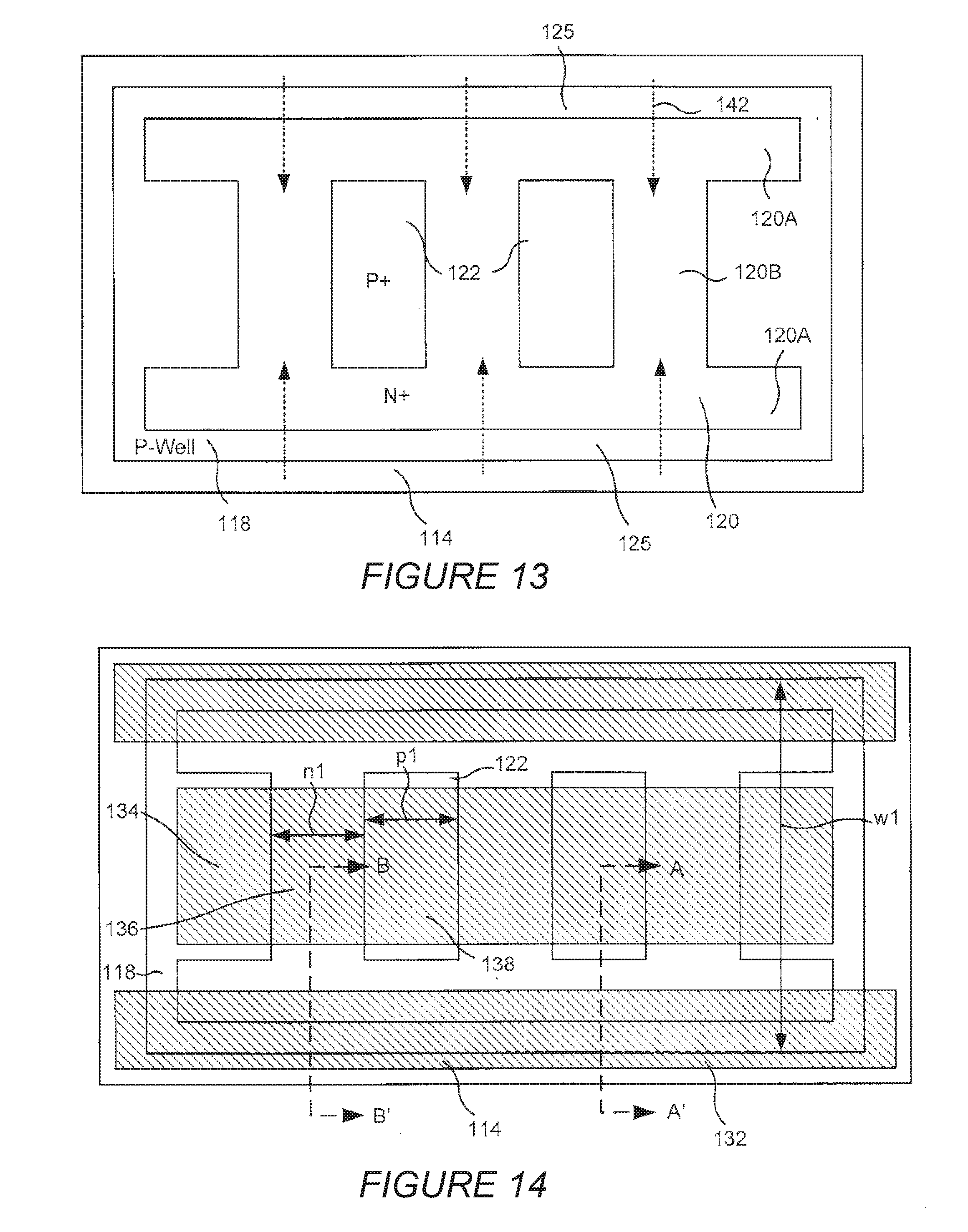
[0022] FIG. 7 is a circuit diagram of a metal-oxide-semiconductor field effect transistor (MOSFET) device.
[0023] FIG. 8 is a graph illustrating hypothetical on-state current-voltage characteristics for a MOSFET device.
[0024] FIG. 9 is a graph illustrating the effect of source resistance on gate voltage.
[0025] FIG. 10 is a partial cross sectional illustration of a cell of a conventional power MOSFET device.
[0026] FIGS. 11 and 12 are plan views illustrating layouts of conventional power MOSFET devices.
[0027] FIGS. 13 and 14 are plan views illustrating layouts of power MOSFET devices according to some embodiments.
[0028] FIGS. 15 and 16 are partial cross sectional illustrations of a cell of a power MOSFET device according to some embodiments.
[0029] FIG. 17 is a graph showing on-state current-voltage characteristics for a MOSFET device according to some embodiments.
[0030] FIG. 18 is a cross sectional illustration of a cell of a power MOSFET device according to some embodiments.
[0031] FIG. 19 is a cross sectional illustration of a cell of an insulated gate bipolar transistor device according to some embodiments.
[0032] FIG. 20 is a cross sectional illustration of a cell of a p-type insulated gate bipolar transistor device according to some embodiments.
[0033] FIG. 21 is a graph showing current-voltage characteristics of the P-IGBT device of FIG. 20.
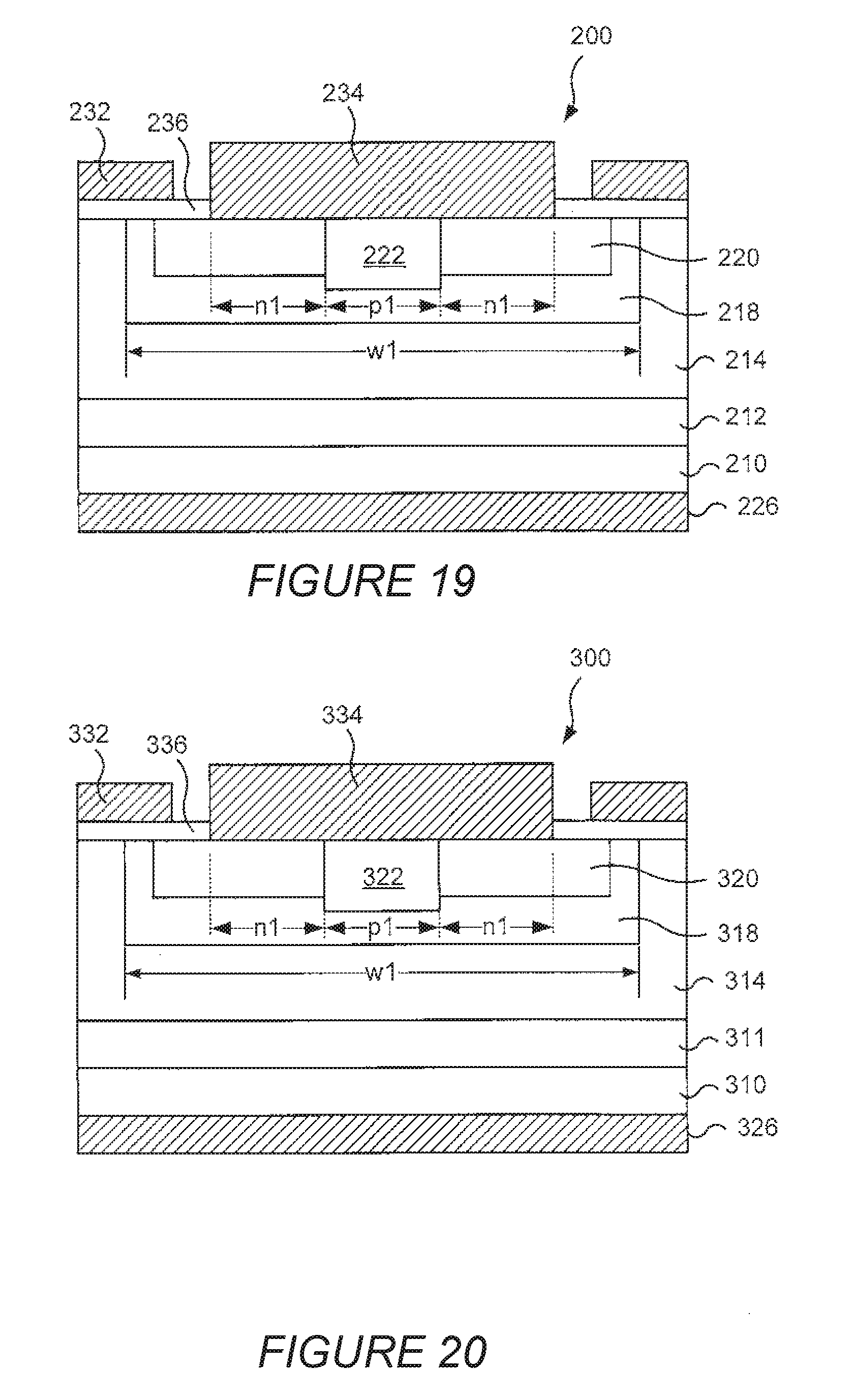
[0034] FIG. 22A is a graph showing voltage blocking characteristics of the p-IGBT of FIG. 20.
[0035] FIG. 22B is a graph showing pulsed on-state current-voltage characteristics of the P-IGBT of FIG. 20.
[0036] FIG. 22C is a graph showing further on-state current-voltage characteristics of the P-IGBTs of FIG. 20 for temperatures ranging from room temperature to 300.degree. C.
[0037] FIG. 22D is a graph showing on-state current-voltage characteristics of the P-IGBTs of FIG. 22 as a function of temperature.
DETAILED DESCRIPTION OF EMBODIMENTS OF THE DISCLOSURE
[0038] Embodiments of the present disclosure now will be described more fully hereinafter with reference to the accompanying drawings, in which embodiments of the disclosure are shown. This disclosure may, however, be embodied in many different forms and should not be construed as limited to the embodiments set forth herein. Rather, these embodiments are provided so that this disclosure will be thorough and complete, and will fully convey the scope of the disclosure to those skilled in the art. Like numbers refer to like elements throughout.
[0039] It will be understood that, although the terms first, second, etc. may be used herein to describe various elements, these elements should not be limited by these terms. These terms are only used to distinguish one element from another. For example, a first element could be termed a second element, and, similarly, a second element could be termed a first element, without departing from the scope of the present disclosure. As used herein, the term "and/or" includes any and all combinations of one or more of the associated listed items.
[0040] The terminology used herein is for the purpose of describing particular embodiments only and is not intended to be limiting of the disclosure. As used herein, the singular forms "a", "an" and "the" are intended to include the plural forms as well, unless the context clearly indicates otherwise. It will be further understood that the terms "comprises" "comprising," "includes" and/or "including" when used herein, specify the presence of stated features, integers, steps, operations, elements, and/or components, but do not preclude the presence or addition of one or more other features, integers, steps, operations, elements, components, and/or groups thereof.
[0041] Unless otherwise defined, all terms (including technical and scientific terms) used herein have the same meaning as commonly understood by one of ordinary skill in the art to which this disclosure belongs. It will be further understood that terms used herein should be interpreted as having a meaning that is consistent with their meaning in the context of this specification and the relevant art and will not be interpreted in an idealized or overly formal sense unless expressly so defined herein.
[0042] It will be understood that when an element such as a layer, region or substrate is referred to as being "on" or extending "onto" another element, it can be directly on or extend directly onto the other element or intervening elements may also be present. In contrast, when an element is referred to as being "directly on" or extending "directly onto" another element, there are no intervening elements present. It will also be understood that when an element is referred to as being "connected" or "coupled" to another element, it can be directly connected or coupled to the other element or intervening elements may be present. In contrast, when an element is referred to as being "directly connected" or "directly coupled" to another element, there are no intervening elements present.
[0043] Relative terms such as "below" or "above" or "upper" or "lower" or "horizontal" or "lateral" or "vertical" may be used herein to describe a relationship of one element, layer or region to another element, layer or region as illustrated in the figures. It will be understood that these terms are intended to encompass different orientations of the device in addition to the orientation depicted in the figures.
[0044] Embodiments of the disclosure are described herein with reference to cross-section illustrations that are schematic illustrations of idealized embodiments (and intermediate structures) of the disclosure. The thickness of layers and regions in the drawings may be exaggerated for clarity. Additionally, variations from the shapes of the illustrations as a result, for example, of manufacturing techniques and/or tolerances, are to be expected. Thus, embodiments of the disclosure should not be construed as limited to the particular shapes of regions illustrated herein but are to include deviations in shapes that result, for example, from manufacturing. For example, an implanted region illustrated as a rectangle will, typically, have rounded or curved features and/or a gradient of implant concentration at its edges rather than a discrete change from implanted to non-implanted region. Likewise, a buried region formed by implantation may result in some implantation in the region between the buried region and the surface through which the implantation takes place. Thus, the regions illustrated in the figures are schematic in nature and their shapes are not intended to illustrate the actual shape of a region of a device and are not intended to limit the scope of the disclosure.
[0045] Some embodiments of the disclosure are described with reference to semiconductor layers and/or regions which are characterized as having a conductivity type such as n-type or p-type, which refers to the majority carrier concentration in the layer and/or region. Thus, n-type material has a majority equilibrium concentration of negatively charged electrons, while p-type material has a majority equilibrium concentration of positively charged holes. Some material may be designated with a "+" or "-" (as in n+, n-, p+, p-, n++, n--, p++, p--, or the like), to indicate a relatively larger ("+") or smaller ("-") concentration of majority carriers compared to another layer or region. However, such notation does not imply the existence of a particular concentration of majority or minority carriers in a layer or region.
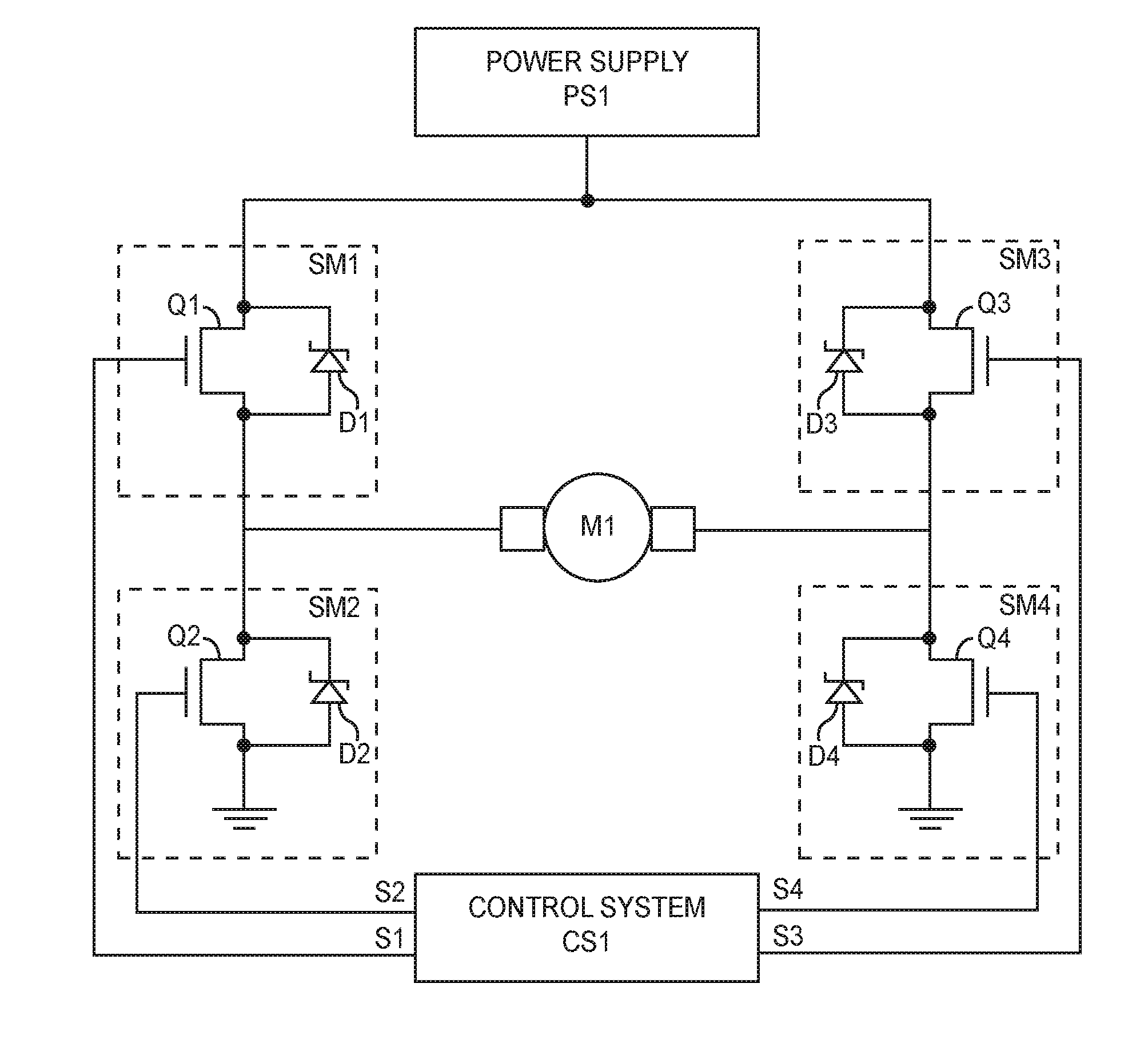
[0046] An exemplary system that employs a power module is illustrated in FIG. 1. As depicted, the power module can include four switch modules SM1-SM4, which are controlled by a control CS1 to deliver power from a power supply PS1 to a load in a controlled manner. The switch modules SM1 and SM2 form a first half of an H-bridge, while switch modules SM3 and SM4 form a second half of the H-bridge. As noted, power modules are often used to drive an inductive load, such as that provided by a direct current (DC) motor M1. The details of the switch modules SM1-SM4 are described in further detail below.
[0047] For now, assume the switch modules SM1-SM4 can include at least one transistor in parallel with an internal or external diode that is connected in anti-parallel with the transistor. The transistors are illustrated as metal oxide field effect transistors (MOSFETs), and the diodes are illustrated as Schottky diodes for purposes of description. The MOSFETs may be replaced with other types of transistors, such as bipolar transistors, including insulated gate bipolar transistors (IGBTs), and various kinds of field effect transistors (FETs), such as junction field effect transistors (JFETs), and high electron mobility transistors (HEMTs). Similarly, the Schottky diodes may be replaced with traditional p-n diodes.
[0048] As illustrated, switch module SM1 may include either an n-channel or p-channel MOSFET Q1 that has a Schottky diode D1 connected in anti-parallel across the drain and source terminals of the MOSFET Q1. Switch modules SM2-SM4 are similarly configured. Switch module SM2 includes an n-channel MOSFET Q2 that has a Schottky diode D2 connected in anti-parallel across the drain and source terminals of the MOSFET Q2. Switch module SM3 may include either an n-channel or p-channel MOSFET Q3 that has a Schottky diode D3 connected in anti-parallel across the drain and source terminals of the MOSFET Q3. Switch module SM4 includes an n-channel MOSFET Q4 that has a Schottky diode D4 connected in anti-parallel across the drain and source terminals of the MOSFET Q4.
[0049] The switch modules SM1 and SM3 are considered on the "high" side, and the switch modules SM2 and SM4 are considered on the "low" side of the power module. The drains of MOSFETs Q1 and Q3 and the cathodes of diodes D1 and D3 are coupled together and to the power supply PS1. The source of MOSFET Q1, the anode of diode D1, the drain of MOSFET Q2, and the cathode of diode D2 are coupled together and to a first terminal of the motor M1. The source of MOSFET Q3, the anode of diode D3, the drain of MOSFET Q4, and the cathode of diode D4 are coupled together and to a second terminal of the motor M1. Finally, the sources of MOSFETs Q2 and Q4 and the anodes of diodes D2 and D4 are coupled to ground. The gates of MOSFETs Q1-Q4 are respectively driven by control signals S1-S4, which are provided by the control system CS1. Assume the motor M1 may be driven in both forward and reverse directions.
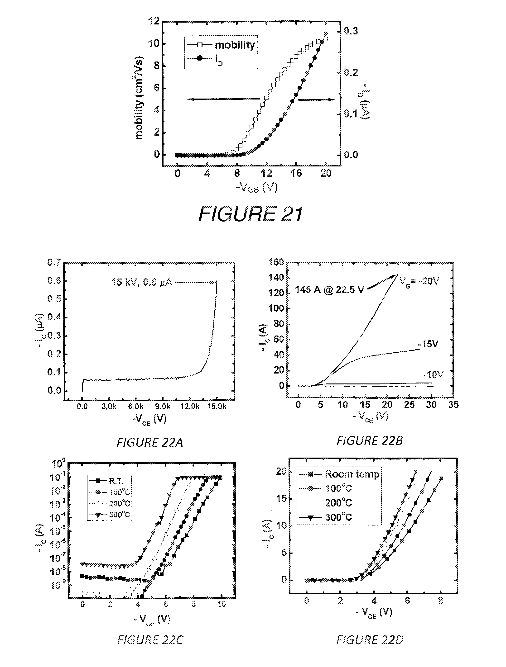
[0050] For forward operation, assume control signals S1-S4 are configured to turn on MOSFETs Q2 and Q3 and turn off MOSFETs Q1 and Q4, which corresponds to driving the motor M1 in a forward direction. As illustrated in FIG. 2, a forward current i.sub.f flows from the power supply PS1 through MOSFET Q3, the motor M1, and the MOSFET Q2 to ground. If MOSFETs Q2 and Q3 stay on, the maximum forward current i.sub.f is provided and the motor M1 will turn in the forward direction at a maximum speed, with maximum torque, or a combination thereof.
[0051] To control the speed or torque, one or both of the MOSFETs Q2 and Q3 may be switched off and on at a duty cycle that corresponds to the speed or torque desired from the motor M1. As a result, the voltage supplied to the motor M1 is pulse width modulated, wherein the on-to-off switching ratio of the MOSFETs Q2 and Q3 dictates the average voltage presented to the motor M1. The inductive nature of the motor M1 tries to keep the forward current i.sub.f constant, and as a result, averages the voltage presented to the motor M1 to a level corresponding to the on-to-off switching ratio of the MOSFETs Q2 and Q3. The average voltage presented to the motor M1 dictates the forward current i.sub.f that is passed through the motor M1, and thus, controls the actual speed or torque of the motor M1.
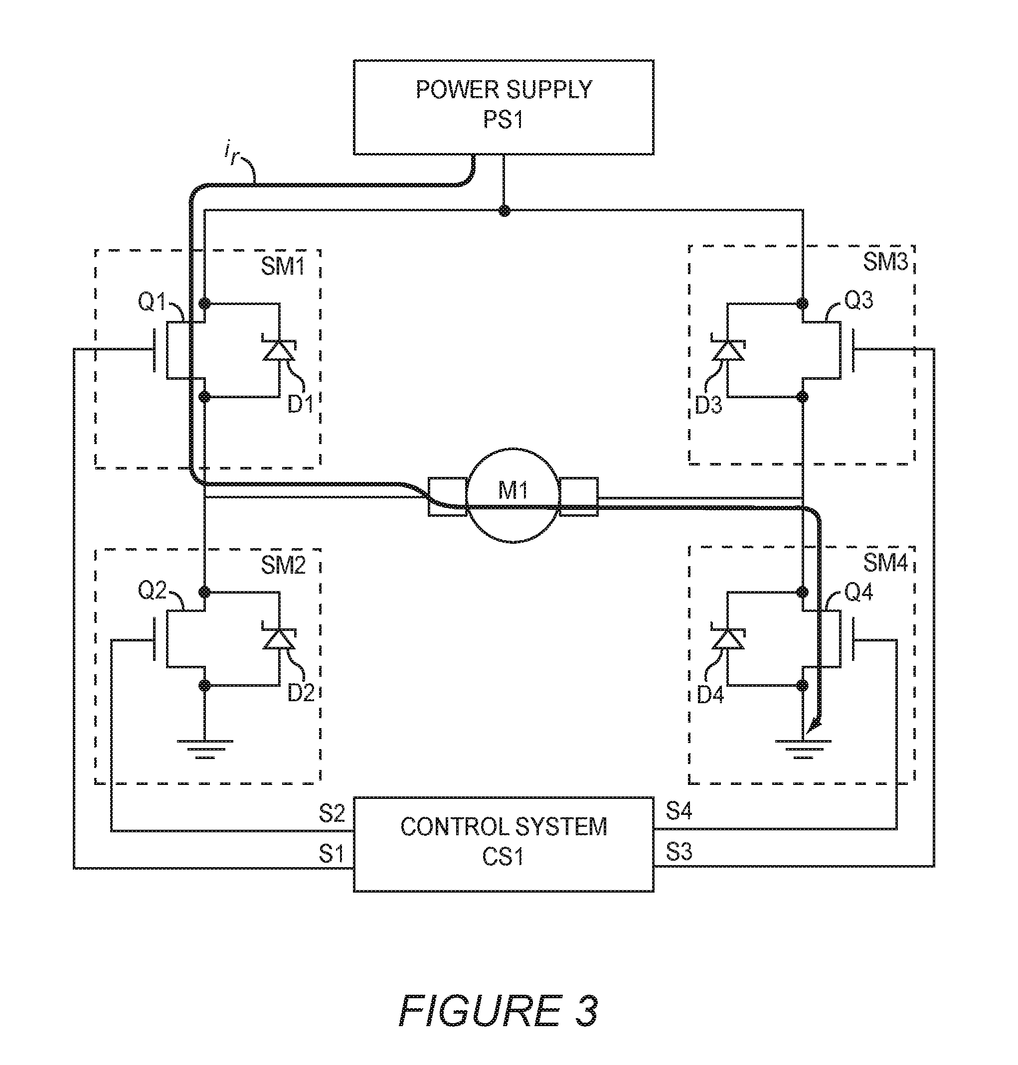
[0052] For reverse operation, assume control signals S1-S4 are configured to turn on MOSFETs Q1 and Q4 and turn off MOSFETs Q2 and Q3. As illustrated in FIG. 3, a reverse current i.sub.r flows from the power supply PS1 through MOSFET Q1, the motor M1, and the MOSFET Q4 to ground. If MOSFETs Q1 and Q4 stay on, the maximum reverse current i.sub.r is provided and the motor M1 will turn in the reverse direction at a maximum speed, with maximum torque, or a combination thereof. Notably, the term "reverse" when used as an adjective in the term "reverse current i.sub.r," merely refers to the direction of operation for the motor M1. The arrows provided in FIGS. 2 and 3, respectively, indicate the direction of current flow for both the forward current i.sub.f and the reverse current i.sub.r.
[0053] As described above, the various MOSFETs Q1-Q4 may be turned on and off at a relatively high frequency to provide pulse width modulated voltage to the motor M1 for either forward or reverse operation as well as to switch from forward operation to reverse operation. When a pair of MOSFETs, such as MOSFETs Q2 and Q3 transition from an on-state to an off-state during forward operation, the forward current i.sub.f continues to flow through the motor M1 after the MOSFETs Q2 and Q3 are turned off, due to the electromagnetic field that is present in the inductive windings of the motor M1. At this point, all of the MOSFETs Q1-Q4 are off, yet the forward current i.sub.f remains flowing through the motor M1. Since the forward current i.sub.f cannot flow through any of the MOSFETS Q1-Q4 to a lower potential node, one or more of the Schottky diodes D1 though D4 may become forward biased and provide a path for the forward current i.sub.f to flow to either ground or the power supply PS1.
[0054] To increase the power handling of a switch module SM1-SM4, each of the MOSFETs Q1-Q4 may represent an array of effectively parallel transistors. Similarly, each of the Schottky diodes D1-D4 may represent an array of effectively parallel diodes. This concept is represented in FIG. 4 where an exemplary embodiment of switch module SM1 is illustrated. The other switch modules SM2-SM3 may be similarly configured.
[0055] As illustrated, switch module SM1 includes an array of MOSFETs Q1.sub.1-Q1.sub.N, which are effectively coupled in parallel, such that the drains are all coupled together and to the power supply PS1; the sources are all coupled together and to the motor M1 and switch module SM2; and the gates are coupled together and to the control system C1 (control signal S1). The Schottky diodes D1.sub.1-D1.sub.N are coupled in anti-parallel across the drain and sources of the MOSFETs Q1.sub.1-Q1.sub.N. The number (N) of MOSFETs Q1.sub.1-Q1.sub.N and Schottky diodes D1.sub.1-D1.sub.N may range from two to more than 100, depending on the capability of each individual device and the application. Notably, there may be two or more Schottky diodes D1 for each MOSFET Q1, even though there is only a one-to-one relationship in the illustration.
[0056] FIGS. 5 and 6 show top and perspective views of an exemplary power module. With reference to FIG. 5, rectangular housing H1 is provided with an interior chamber that holds one or more printed circuit boards PCB1 and PCB2. For clarity, the printed circuit boards PCB1 and PCB2 are not shown in FIG. 6. Each printed circuit board PCB1 and PCB2 is shown as having multiple transistors Q and diodes D that represent the primary components of the switch modules SM1-SM4. For example, the high and low side of the first half-H bridge formed by switch modules SM1 and SM2 are provided on printed circuit board PCB1, while the high and low side of the second half-H bridge formed by switch modules SM3 and SM4 are provided on printed circuit board PCB2. Together, the first and second half-H bridges form the above-described full-H bridge.
[0057] The necessary interconnects between the components on the printed circuit boards PCB1 and PCB2 are provided by metal traces (not shown) on the printed circuit boards PCB1 and PCB2. Bond wires may be used to make connections between the printed circuit boards PCB1 and PCB2 and one more connectors or buses B1 and B2. For example, bus B1 may be used to connect switch modules SM2 and SM4 to ground, and bus B2 may be used to connect switch modules SM1 and SM3 to the power supply PS1. These or other connectors may be used for the control signals S1-S4. The printed circuit boards PCB1 and PCB2 may be mounted to a mounting structure that is affixed to the housing H1. As illustrated, the mounting structure is a planar heat sink HS1 that also functions to dissipate heat generated by the switch modules SM1-SM4.
[0058] Again, the H-bridge configuration of the power module is just one of many available designs for power modules, especially those used to drive inductive loads. Alternatives to the H-bridge configuration for the power module include a half-H bridge and like known power switching or control circuits.
[0059] Regardless of the type of configuration of the power module, one metric for measuring the power handling capabilities of the device is current density of one of the switch modules SM1-SM4. This switch module current density is defined as the ratio of the maximum average current that a single switch module SM1-SM4 can handle to the interior area of the housing H1 that is allocated to the single switch module SM1-SM4. For the illustrated example, there are four switch modules SM1-SM4 of equal size. As such, the interior area of the housing H1 that is allocated to a single switch module SM1-SM4 is one-fourth (1/4) the total interior area of the housing H1.
[0060] For example, assume the interior area of the housing H1 is 100 cm.sup.2, and the maximum average current handling of one of the switch modules SM1-SM4 is 250 amperes. As such, the interior area of the housing H1 that is allocated to a single switch module SM1-SM4 is one-fourth of 100 cm.sup.2, or 25 cm.sup.2. The switch module current density is calculated by dividing the maximum average current handling of 250 amperes by the interior area of the housing H1 that is allocated to the single switch module SM1-SM4, which yields 10 amperes/cm.sup.2.
[0061] The interior area of the housing H1 is defined as the maximum (two-dimensional) cross-sectional area of the interior of the housing H1 wherein the plane of measurement is along the plane in which one or more printed circuit boards PCB1 and PCB2 or one or more semiconductor die that provide the switch modules SM1-SM4 reside. For the illustrated example in FIG. 5, the interior area is defined by the perimeter of the inside wall of the housing H1. Notably, since the housing H1 may have various shapes and configurations in addition to the rectangular configuration shown in FIGS. 5 and 6, the interior areas need not be rectangular and the perimeter of the interior areas will follow the interior sidewalls of the housing H1. In one embodiment, the switch module current density is about 10 amperes/cm.sup.2 or greater. In another embodiment, the switch module current density is about 12 amperes/cm.sup.2 or greater. In another embodiment, the switch module current density is about 15 amperes/cm.sup.2 or greater.
[0062] The following description outlines several transistor configurations that can be used in the power module as MOSFETs Q1.sub.N-Q4.sub.N or alternatives thereto. Other transistor configurations may be employed. Some embodiments of the disclosure provide silicon carbide (SiC) insulated gate devices that are suitable for high power and/or high temperature applications.
[0063] FIG. 7 is a circuit diagram of a metal oxide semiconductor field effect transistor (MOSFET) device 10. As shown therein, a MOSFET device generally includes three terminals, namely, a drain terminal (D), a source terminal (S) and a gate terminal (G). The gate-to-source voltage of the device is denoted V.sub.GS, while the drain-to-source voltage of the device is denoted V.sub.DS. The device has a built in source resistance R.sub.S and a built-in drain resistance R.sub.D based on the physical characteristics of the device. The voltage over the built-in source resistance R.sub.S is denoted V.sub.Rs.
[0064] In a MOSFET device, current passing through a channel of the device from the drain to the source is regulated by applying a voltage to the gate. The gate is insulated from the channel by a gate insulator, such as silicon dioxide. As the voltage on the gate terminal is increased, current passing through the device may increase.
[0065] FIG. 8 is a graph illustrating hypothetical curve 102 and actual 104 on-state current-voltage characteristics for a MOSFET device for a given gate-to-source voltage (V.sub.GS). As shown in FIG. 8, for a given gate voltage, the current through the device (I.sub.D) increases as the voltage between the drain and source (V.sub.DS) increases, up to a saturation point. In actual devices, the actual saturation current of a transistor is typically less than the ideal saturation current. Part of the reason for this relates to the source resistance of the device.
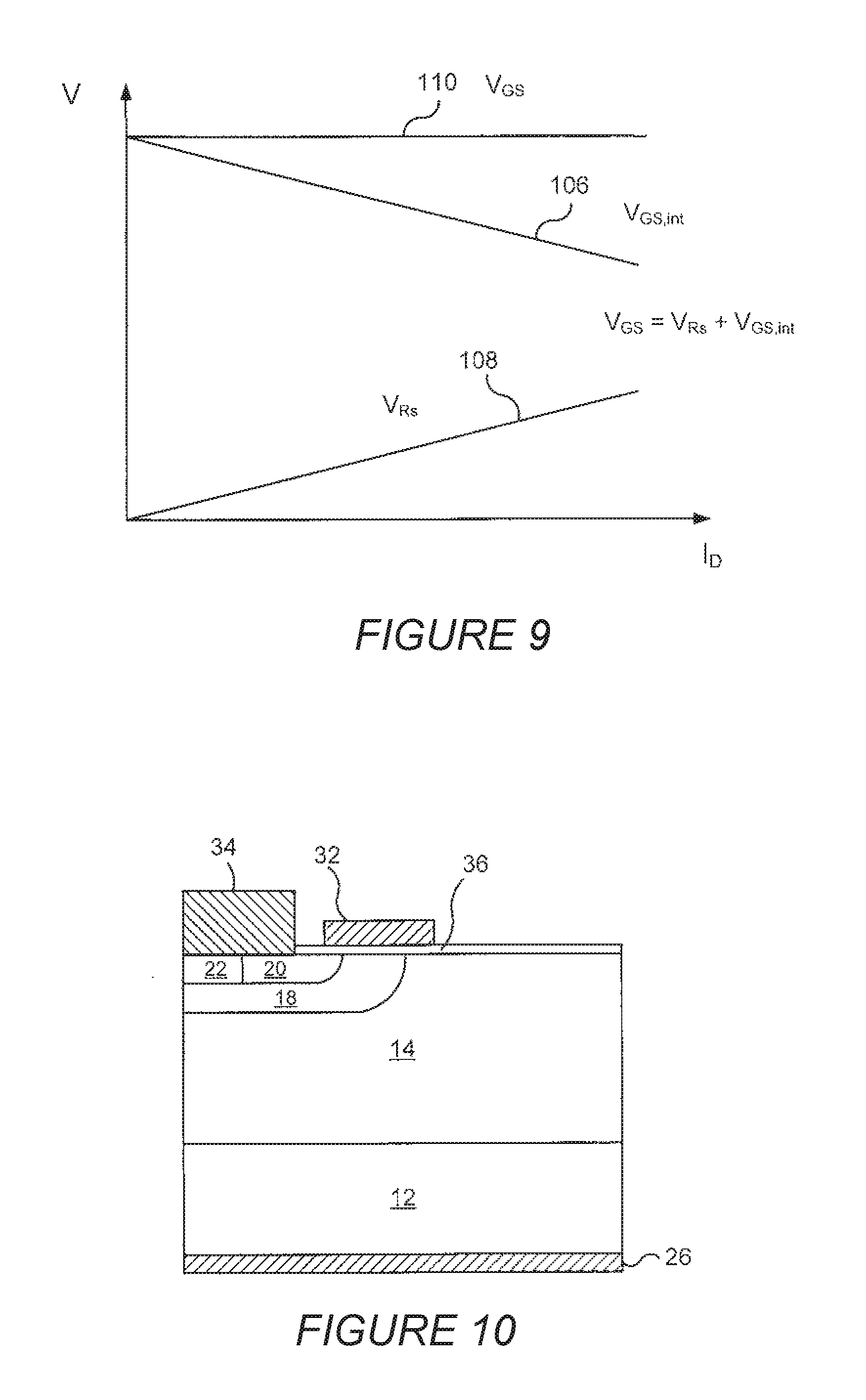
[0066] In particular, as the drain current I.sub.D passing through the device increases, the amount of voltage dropped over the source resistance R.sub.S increases in direct proportion. FIG. 9 is a graph illustrating the effect of source resistance on gate voltage. In FIG. 9, the voltage from the gate terminal to the source terminal is denoted V.sub.GS. A portion of the gate voltage V.sub.GS applied to the device across the gate and source terminals is dropped over the internal source resistance R.sub.S of the device. That portion of the gate voltage is denoted V.sub.Rs in FIG. 9. The remainder of the gate-to-source voltage appears as a voltage across the gate insulator, denoted V.sub.GS,int in FIG. 9. Thus, V.sub.GS is equal to the sum of V.sub.Rs and V.sub.GS,int.
[0067] As shown in FIG. 9, the gate-to-source voltage may remain constant as the drain current increases. However, the portion of the gate voltage V.sub.GS that is dropped over the internal source resistance of the device, V.sub.Rs, increases as the drain current I.sub.D increases, while the portion of the gate-to-source voltage that appears as a voltage across the gate insulator, V.sub.GS,int, decreases as the drain current I.sub.D increases.
[0068] Thus, as the drain current increases the portion of the gate voltage that is being used to maintain the channel decreases, which may cause the device to go into saturation at a lower level of drain-to-source voltage. Accordingly, a high source resistance can adversely affect the operation of a MOSFET or other insulated gate controlled device.
[0069] A unit cell of a MOSFET structure according to some embodiments is shown in FIG. 10. The device of FIG. 10 includes an n- drift epitaxial layer 14 on an n-type, 8.degree. off-axis 4H-SiC substrate 12. The n- drift layer 14 may have a thickness of about 100 .mu.m to about 120 .mu.m, and may be doped with n-type dopants at a doping concentration of about 2.times.10.sup.14 cm.sup.-3 to about 6.times.10.sup.14 cm.sup.-3 for a blocking capability of about 10 kV. Other doping concentrations/voltage blocking ranges are also possible. For a 1200V MOSFET device, the substrate may be 4.degree. off-axis 4H-SiC and the drift layer may have a thickness of about 10 .mu.m and may be doped with n-type dopants at a doping concentration of about 6.times.10.sup.15 cm.sup.-3.
[0070] The structure further includes a p+ well region 18 and an n+ source region 20 that may be formed by selective implantation of, for example, aluminum and nitrogen, respectively. The junction depth of the p+ well region 18 may be about 0.5 .mu.m, although other depths are possible. The structure further includes a p+ contact region 22 that extends from a surface of the drift layer 14 into the p+ well region 18. A junction termination (not shown) may be provided around the device periphery.
[0071] All of the implanted dopants may be activated by annealing the structure at a temperature of about 1600.degree. C. with a silicon over pressure and/or covered by an encapsulation layer such as a graphite film. A high temperature anneal may damage the surface of the silicon carbide epitaxy without these conditions. The silicon overpressure may be provided by the presence of silane, or the close proximity of silicon carbide coated objects that provide a certain amount of silicon overpressure. Alternatively or in combination with silicon overpressure, a graphite coating may be formed on the surface of the device. Prior to annealing the device to activate the implanted ions, a graphite coating may be applied to the top/front side of the structure in order to protect the surface of the structure during the anneal. The graphite coating may be applied by a conventional resist coating method and may have a thickness of about 1 .mu.m. The graphite coating may be heated to form a crystalline coating on the drift layer 14. The implanted ions may be activated by a thermal anneal that may be performed, for example, in an inert gas at a temperature of about 1600.degree. C. or greater. In particular the thermal anneal may be performed at a temperature of about 1600.degree. C. in argon for 5 minutes. The graphite coating may help to protect the surface of the drift layer 14 during the high temperature anneal.
[0072] The graphite coating may then be removed, for example, by ashing and thermal oxidation.
[0073] After implant annealing, a field oxide of silicon dioxide (not shown) having a thickness of about 1 .mu.m may be deposited and patterned to expose the active region of the device.
[0074] A gate oxide layer 36 may be formed by a gate oxidation process, with a final gate oxide thickness of 400-600 .ANG..
[0075] In particular, the gate oxide may be grown by a dry-wet oxidation process that includes a growth of bulk oxide in dry O.sub.2 followed by an anneal of the bulk oxide in wet O.sub.2 as described, for example, in U.S. Pat. No. 5,972,801, the disclosure of which is incorporated herein by reference in its entirety. As used herein, anneal of oxide in wet O.sub.2 refers to anneal of an oxide in an ambient containing both O.sub.2 and vaporized H.sub.2O. An anneal may be performed in between the dry oxide growth and the wet oxide growth. The dry O.sub.2 oxide growth may be performed, for example, in a quartz tube at a temperature of up to about 1200.degree. C. in dry O.sub.2 for a time of at least about 2.5 hours. Dry oxide growth is performed to grow the bulk oxide layer to a desired thickness. The temperature of the dry oxide growth may affect the oxide growth rate. For example, higher process temperatures may produce higher oxide growth rates. The maximum growth temperature may be dependent on the system used.
[0076] In some embodiments, the dry O.sub.2 oxide growth may be performed at a temperature of about 1175.degree. C. in dry O.sub.2 for about 3.5 hours. The resulting oxide layer may be annealed at a temperature of up to about 1200.degree. C. in an inert atmosphere. In particular, the resulting oxide layer may be annealed at a temperature of about 1175.degree. C. in Ar for about 1 hour. The wet O.sub.2 oxide anneal may be performed at a temperature of about 950.degree. C. or less for a time of at least about 1 hour. The temperature of the wet O.sub.2 anneal may be limited to discourage further thermal oxide growth at the SiC/SiO.sub.2 interface, which may introduce additional interface states. In particular, the wet O.sub.2 anneal may be performed in wet O.sub.2 at a temperature of about 950.degree. C. for about 3 hours. The resulting gate oxide layer may have a thickness of about 500 .ANG..
[0077] In some embodiments, the dry O.sub.2 oxide growth may be performed at a temperature of about 1175.degree. C. in dry O.sub.2 for about 4 hours. The resulting oxide layer may be annealed at a temperature of up to about 1175.degree. C. in an inert atmosphere. In particular, the resulting oxide layer may be annealed at a temperature of about 1175.degree. C. in Ar for about a time duration ranging from 30 min to 2 hours. Then the oxide layer receives an anneal in NO ambient at a temperature ranging from 1175.degree. C. to 1300C, for a duration ranging from 30 minutes to 3 hours. The resulting gate oxide layer may have a thickness of about 500 .ANG..
[0078] After formation of the gate oxide 34, a polysilicon gate 32 may be deposited and doped, for example, with boron followed by a metallization process to reduce the gate resistance. Al/Ni contacts may be deposited as the p-type ohmic source contact metal 34, and Ni as the n-type drain contact metal 26. All contacts may be sintered in a Rapid Thermal Annealer (RTA), and thick Ti/Au layers may be used for pad metals.
[0079] Referring to FIG. 10, the source resistance of a MOSFET device has two primary components, namely, the contact resistance R.sub.C between the source ohmic contact 34 and the source region 20, and the sheet resistance R.sub.sheet in the source region 20 between the source ohmic contact 34 and the channel. Thus, R.sub.S=R.sub.C+R.sub.sheer. In a conventional silicon-based MOSFET device, the sheet resistance R.sub.sheet is the dominant factor in determining the source resistance, because it is possible to form very low resistivity ohmic contacts to silicon and other narrow-bandgap semiconductors. However, in wide bandgap semiconductors (i.e., semiconductors having a bandgap greater than about 2.0 V), including compound semiconductor materials, such as silicon carbide and gallium nitride, diamond, and ZnO, the contact resistance R.sub.C may be the dominant contributor to the source resistance. In particular, it is difficult to form very low resistivity ohmic contacts to silicon carbide and other wide bandgap materials because of the high energy barrier associated with such materials.
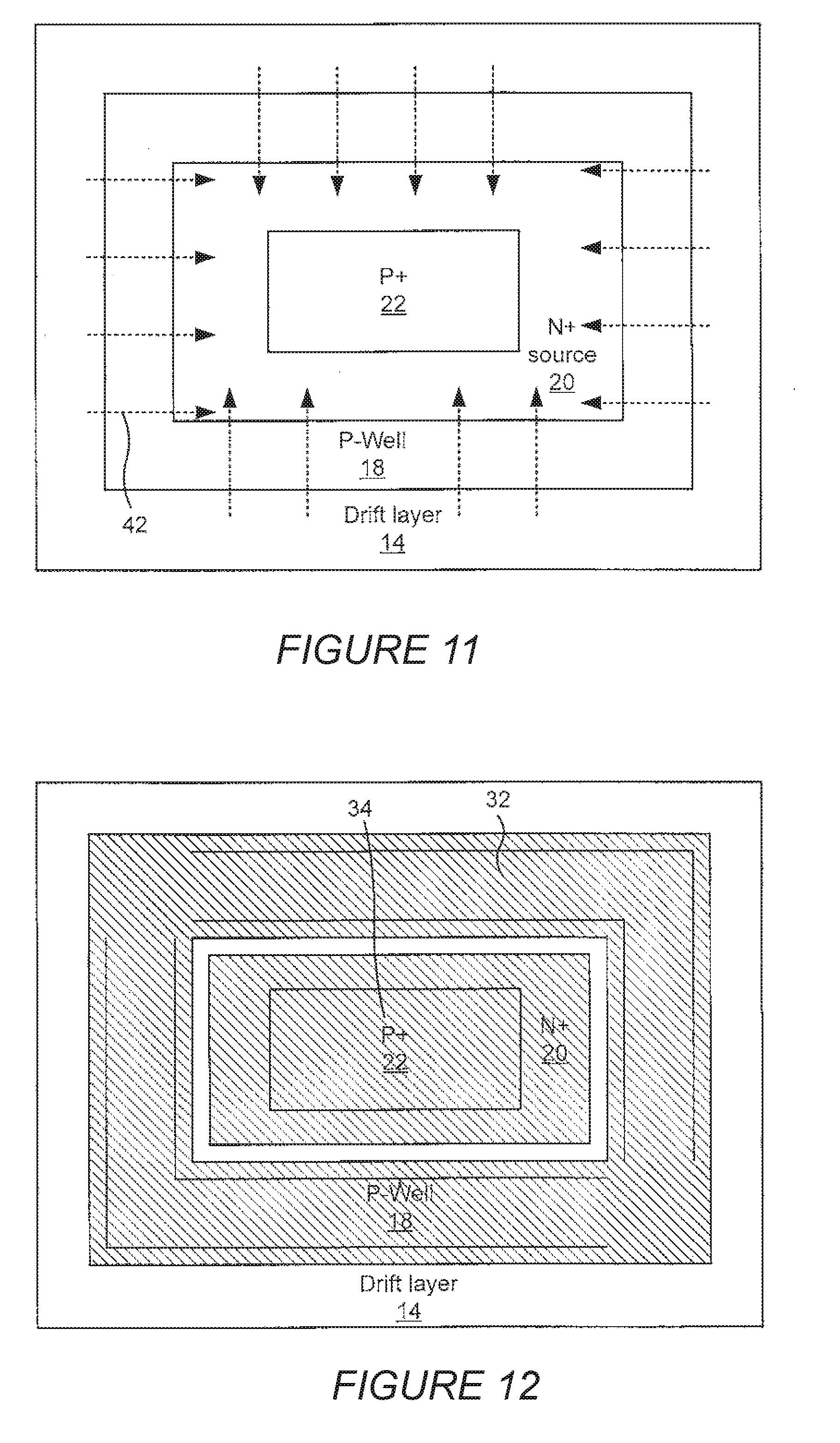
[0080] FIGS. 11 and 12 are plan views illustrating layouts of conventional power MOSFET devices. In a conventional power MOSFET device, the layout is designed to reduce or minimize sheet resistance under the assumption that contact resistance is less important than sheet resistance. Thus, referring to FIG. 11, a conventional power MOSFET device typically includes a p-well 18 formed in a drift layer 14, an n+ source region 20 in the p-well 18, and a p+ contact region 22 in the n+ source region 20. Referring to FIG. 12, a source contact 34 is formed on the n+ source region 20 and the p+ contact region 22. A gate 32 is formed over the p-well 18 and overlaps the periphery of the n+ source region 20 and adjacent portions of the drift layer 14. Current flow from the drain to the source is indicated by the arrows 42 in FIG. 11.
[0081] As noted above, in a wide bandgap semiconductor material system, the source resistance may be more affected by the contact resistance of the source ohmic contact than by the sheet resistance of the source layer. Accordingly, to decrease the source resistance of a wide bandgap power semiconductor device, it may be desirable to decrease the contact resistance of the source ohmic contact. In general, contact resistance can be decreased by increasing the minimum dimension of the contact, which is the smallest dimension of the contact in any direction. However, simply increasing the minimum dimension of the source ohmic contact of an electronic device can undesirably increase the cell to cell spacing, or pitch, of the device. The pitch of a MOSFET device may be proportional to the width of the p-well region of the device. Increasing the pitch of the device reduces the density of the devices that can be formed on a single substrate, reducing the devices yielded and increasing manufacturing costs.
[0082] According to some embodiments, an insulated gate device layout is provided that increases the minimum dimension of the source ohmic contact without increasing the pitch of the device and/or the width of the p-well region of the device. A device layout according to some embodiments may increase the sheet resistance of the device. Such an effect may be highly undesirable in a device based on a narrow bandgap semiconductor material. However, since sheet resistance is not the dominant factor in determining source resistance of a wide bandgap device, such a tradeoff may be acceptable for wide bandgap devices. In devices according to some embodiments, a ratio of the source sheet resistance to the source contact resistance may be greater than 0.75 (i.e. R.sub.sheet/R.sub.C>0.75). In some embodiments, the device may have a source contact resistance that is less than the source sheet resistance. That is, in some embodiments, the ratio of the source sheet resistance to the source contact resistance may be greater than 1 (i.e. R.sub.sheet/R.sub.C>1), and in further embodiments, the ratio of the source sheet resistance to the source contact resistance may be greater than 5.
[0083] FIGS. 13 and 14 are plan views illustrating layouts of MOSFET device cells according to some embodiments, and FIGS. 15 and 16 are partial cross sectional illustrations of a cell of a MOSFET device according to some embodiments. In particular, FIG. 15 is a cross section taken along line A-A' of FIG. 13, while FIG. 16 is a cross section taken along line B-B' of FIG. 14.
[0084] The device shown in FIGS. 13-16 includes an n- drift epitaxial layer 114 on an n-type, 8.degree. off-axis 4H-SiC substrate 112. The n- drift layer 114 may have a thickness of about 100 .mu.m to about 120 .mu.m, and may be doped with n-type dopants at a doping concentration of about 2.times.10.sup.14 cm.sup.-3 to about 6.times.10.sup.14 cm.sup.-3 for a blocking capability of about 10 kV. For a 1200V MOSFET device, the substrate may be 4.degree. off-axis 4H-SiC and the drift layer may have a thickness of about 10 .mu.m and may be doped with n-type dopants at a doping concentration of about 6.times.10.sup.15 cm.sup.-3.
[0085] The structure further includes a p+ well region 118 and an n+ source region 120 that may be formed by selective implantation of, for example, aluminum and nitrogen, respectively. The junction depth of the p+ well region 118 may be about 0.5 .mu.m. The structure further includes a plurality of p+ contact regions 122 that extend from a surface of the drift layer 114 into the p+ well region 118. A junction termination (not shown) may be provided around the device periphery.
[0086] Referring to FIG. 13, the n+ source region 120 includes a pair of lateral source regions 120A that are parallel to opposing channel regions 125 in the p-well 118. A plurality of source contact regions 120B extend between the lateral source regions 120A, and the plurality of p+ contact regions 122 are provided between the source contact regions 120B.
[0087] Referring to FIG. 14, gate contacts 132 are formed over the channel regions 125 and overlap the lateral source regions 120A. A source ohmic contact 134 is formed across the source contact regions 120B and the p+ contact regions 122. The source ohmic contact 134 overlaps the source contact regions 120B in a source contact region 136. The source ohmic contact 134 overlaps the p+ contact regions 122 in a body contact region 138.
[0088] The portion of the source contact regions 120B contacted by the source ohmic contact 134 may have a minimum dimension that is larger than the minimum dimension that can be obtained for a conventional layout such as the layout shown in FIGS. 11 and 12 for a similar pitch/p-well size. Accordingly, the source contact resistance may be reduced without substantially increasing the device pitch/p-well size. The "minimum dimension" of a feature refers to the smallest width of the feature in any cross section of the feature. For example, the minimum dimension p1 of the body contact region 138, the minimum dimension n1 of the n-type contact region 136, and the minimum dimension w1 of the p-well region 118 are shown in FIG. 14.
[0089] In a device having a layout as shown in FIGS. 13 and 14, current flow to the source contact flows through the source contact regions 120B, as indicated by the arrows 142 in FIG. 13. The source contact regions 120B may have an increased sheet resistance compared to the source region of a device having a conventional layout as shown in FIGS. 11 and 12. However, the increase in sheet resistance may be more than compensated by the decrease in contact resistance, thus providing an overall decrease in the source resistance of the device.
[0090] FIG. 17 is a graph of on-state current-voltage characteristics for a 7 mm.times.8 mm 1200 V silicon carbide MOSFET device according to some embodiments. In the device characteristics illustrated in FIG. 17, a drain current (I.sub.D) of 377 A was measured at a forward voltage drain-to-source voltage (V.sub.DS) of 3.8 V. The current density, normalized to the active area, was over 750 A/cm.sup.2.
[0091] The on-resistance of a MOSFET device is affected by the drain resistance, the channel resistance and the source resistance of the device. Accordingly, reducing the source resistance of the device also reduces the on-resistance of the device.
[0092] A wide bandgap MOSFET device having a layout according to some embodiments may be capable of substantially increased saturation current due to the lower on-resistance of the device and the fact that increased current levels have less of a de-biasing effect on the gate. That is, because of the lower source resistance, less voltage will be developed over the source resistance as the drain current increases. Thus, more of the gate-to-source voltage is applied to the channel of the device.
[0093] FIG. 18 is an idealized cross section of a device having a layout in accordance with some embodiments. In particular, FIG. 18 illustrates some dimensions of a device having a layout in accordance with some embodiments. For example, as shown in FIG. 18, the minimum dimension of the implanted cell area (i.e. the p-well 118) is denoted as width w1 in FIG. 18. It will be appreciated, however, that the minimum dimension of the p-well 118 may occur in a dimension that is different from the plane of the device illustrated in FIG. 18. For example, the minimum dimension of the p-well 118 may occur in a dimension that is perpendicular to the plane of the device illustrated in FIG. 18.
[0094] The minimum dimension of the n-type contact area is denoted as width n1 in FIG. 18, while the minimum dimension of the p-type contact area is denoted as width p1 in FIG. 18. The n-type contact area may be defined as the area of overlap between the source ohmic contact 132 and the n+ source region 120, while the p-type contact area may be defined as the area of overlap between the source ohmic contact 132 and the p+ contact regions 122.
[0095] An insulated gate bipolar transistor (IGBT) device 200 according to some embodiments is illustrated in FIG. 19. As shown therein, the IGBT device includes an n- drift epitaxial layer 214 on a p-type epitaxial layer 212. The p-type epitaxial layer 212 is formed on a heavily doped p-type, 8.degree. off-axis 4H-SiC substrate or layer 210. The n- drift layer 214 may have a thickness of about 100 .mu.m to about 120 .mu.m, and may be doped with p-type dopants at a doping concentration of about 2.times.10.sup.14 cm.sup.-3 to about 6.times.10.sup.14 cm.sup.-3 for a blocking capability of about 10 kV.
[0096] The IGBT structure 200 further includes a p+ well region 218 and an n+ source/emitter region 220 that may be formed by selective implantation of, for example, aluminum and nitrogen, respectively. The junction depth of the p+ well region 218 may be about 0.5 .mu.m. The structure 200 further includes a plurality of p+ body contact regions 222 that extend from a surface of the drift layer 214 into the p+ well region 218. The conductivity types may be reversed in some embodiments.
[0097] A gate contact 232 is on a gate insulator 236, a source/emitter contact 234 is on the source contact regions 220 and the body contact regions 222. A collector contact 226 contacts the substrate 210.
[0098] According to some embodiments, a transistor device may have a ratio of n1 to w1 that is greater than 0.2. In further embodiments, a transistor device may have a ratio of n1 to w1 that is greater than about 0.3. In further embodiments, a transistor device may have a ratio of n1 to w1 that is in the range of about 0.2 to 1. In further embodiments, a transistor device may have a ratio of n1 to w1 that is in the range of about 0.3 to 1. In further embodiments, transistor device may have a ratio of n1 to w1 that is greater than 0.5. For example, the minimum dimension n1 of the n-type contact area of a device having a layout according to some embodiments may be about 2 .mu.m for a device having a minimum dimension of the implanted cell area of 6 .mu.m.
[0099] According to some embodiments, a transistor device may have a ratio of p1 to w1 that is greater than 0.2. In further embodiments, a transistor device may have a ratio of p1 to w1 that is greater than about 0.3. In further embodiments, a transistor device may have a ratio of p1 to w1 that is greater than about 0.5. In further embodiments, a transistor device may have a ratio of p1 to w1 that is in the range of about 0.2 to 0.5. In further embodiments, a transistor device may have a ratio of p1 to w1 that is in the range of about 0.2 to 1.
[0100] Some embodiments provide transistor devices having increased current densities. Current density is defined as the total current divided by the area of the chip. For example, a wide bandgap transistor device according to some embodiments may be capable of current densities in excess of 200 A/cm.sup.2 and a blocking voltage of 1000 V or more. A wide bandgap transistor device according to further embodiments may be capable of a current of 100 A or greater at current densities in excess of 200 A/cm.sup.2, a forward voltage drop of less than 5 V and a blocking voltage of 1000 V or more. A wide bandgap transistor device according to still further embodiments may be capable of a current of 100 A or greater at current densities in excess of 300 A/cm.sup.2, a forward voltage drop of less than 5 V and a blocking voltage of 1000 V or more.
[0101] A semiconductor device according to some embodiments has a reverse blocking voltage in excess of 1000 volts and a current density greater than 200 amps per square centimeter at a current greater than 100 A.
[0102] A semiconductor device according to further embodiments has a reverse blocking voltage of 1000 volts or more and a forward current capability greater than 100 A at a forward voltage of 5 volts or less.
[0103] A metal-oxide semiconductor field effect transistor device according to some embodiments has a reverse blocking voltage of 1200 volts or more and a forward current capability greater than 100 A.
[0104] A metal-oxide semiconductor field effect transistor device according to some embodiments has a reverse blocking voltage of 1000 volts or more and a differential on-resistance less than 8 mOhms-cm.sup.2.
[0105] A semiconductor device having a blocking voltage less than 1000 V and configured to pass forward current at a current density greater than 200 amps per square centimeter at a forward voltage drop of 5 V or less.
[0106] Some embodiments may enable wide bandgap transistor devices to achieve drain currents of 100 Amps or higher at a drain to source voltage that is less than 4 Volts in a device having a cell pitch of less than 20 .mu.m. Some embodiments may enable wide bandgap transistor devices to achieve drain currents of 100 Amps or higher at a drain to source voltage that is less than 4 Volts in a device having a cell pitch of less than 10 .mu.m. Some embodiments may enable wide bandgap transistor devices to achieve drain currents of 80 Amps or higher at a drain to source voltage that is less than 5 Volts in a device having a cell pitch of less than 10 .mu.m.
[0107] An IGBT device according to some embodiments with a voltage blocking capability of 10 kV or greater may have a differential specific on-resistance of less than 14 mOhm-cm.sup.2 with a forward voltage drop of 5.2 V or less at a current density of 100 A/cm.sup.2.
[0108] A p-type insulated gate bipolar transistor (p-IGBT) device 300 according to some embodiments is illustrated in FIG. 20. As shown therein, the IGBT device includes a p- drift epitaxial layer 314 on a p-type field stop buffer layer 311 formed on an n-type, 8.degree. off-axis 4H-SiC substrate 310. The p- drift layer 314 may have a thickness of about 100 .mu.m to about 200 .mu.m, and may be doped with p-type dopants at a doping concentration of about 2.times.10.sup.14 cm.sup.-3 to about 6.times.10.sup.14 cm.sup.-3.
[0109] The p-IGBT structure 300 further includes an n+ well region 318 and a p+ source/emitter region 320 that may be formed by selective implantation of, for example, nitrogen and aluminum, respectively. The junction depth of the n+ well region 318 may be about 0.5 .mu.m. The structure 300 further includes a plurality of n+ body contact regions 322 that extend from a surface of the drift layer 314 into the n+well region 318.
[0110] A gate contact 332 is on a gate insulator 336, a source/emitter contact 334 is on the source contact regions 320 and the body contact regions 322. A collector contact 326 contacts the substrate 310.
[0111] A 4H-SiC p-IGBT as shown in FIG. 20 was fabricated using a 2.times.10.sup.14 cm.sup.-3 doped, 140 .mu.m thick p-type epilayer as the drift layer 314, and a 2 .mu.m thick p-type Field-Stop buffer layer 311, with a doping concentration ranging from 1.times.10.sup.17 cm.sup.-3 to 5.times.10.sup.17 cm.sup.3. A multi-zone JTE (15 zone) edge termination structure (not shown) was formed by nitrogen ion implantation. JTE terminations are described, for example, in U.S. Pat. No. 6,002,159, which is incorporated herein by reference. MOS channels were formed on implanted n-wells 318. A 50 nm thick thermally grown oxide layer was used as the gate insulator 336.
[0112] FIG. 21 shows the I.sub.D-V.sub.GS characteristics of the p-IGBT device shown in FIG. 20, with V.sub.DS fixed at -50 mV. The I.sub.D-V.sub.GS characteristics were measured from a test MOSFET with a W/L of 200 .mu.m/200 .mu.m, fabricated on the same wafer. A threshold voltage of -10 V, and a peak MOS channel mobility of 10 cm.sup.2/Vs were extracted from the I.sub.D-V.sub.GS characteristics.
[0113] FIG. 22A shows the blocking characteristics (V.sub.GE=0 V) of a 6.7 mm.times.6.7 mm 4H-SiC P-IGBT, with an active area of 0.16 cm.sup.2 at room temperature. The measurement voltage was limited to -15 kV, due to the limitation of probing equipment. The device showed a leakage current of 0.6 .mu.A, which corresponds to a leakage current density of 1.2 .mu.A/cm.sup.2 at a V.sub.CE of -15 kV. This is the highest blocking voltage ever reported in SiC power switches. FIG. 22B shows the pulsed on-state I-V characteristics of the p-IGBT, measured using a Tektronix 371 curve tracer. The device showed an on-state current of -145 A, which represents a current density of 906 A/cm.sup.2, at a V.sub.CE of -22.5 V and a V.sub.GE of -20 V. No evidence of parasitic thyristor latch-up was observed during this measurement. FIG. 22C shows I.sub.C-V.sub.GE characteristics of the 4H-SiC P-IGBTs for temperatures ranging from room temperature to 300.degree. C. V.sub.CE was fixed at -10V for this measurement. The I-V characteristics shifted towards zero at elevated temperature. However, the device maintained normally-off properties throughout the temperature range. FIG. 22D shows the on-state I-V characteristics as a function of temperature. V.sub.GE was fixed at -20 V for this measurement. A monotonic decrease in forward voltage drop with increasing temperature was observed. This is believed due to the increase in minority carrier (electron) diffusion length, caused by increased carrier lifetime at elevated temperatures.
[0114] Accordingly, a p-IGBT according to some embodiments may have a reverse blocking voltage that is greater than about 10 kV, and in some cases greater than about 13 kV, and that has a forward current capability greater than 5 Amps.
[0115] It will be appreciated that although some embodiments of the disclosure have been described in connection with silicon carbide IGBT and MOSFET devices having n-type drift layers, the present disclosure is not limited thereto, and may be embodied in devices having p-type substrates and/or drift layers. Furthermore, the disclosure may be used in many different types of devices, including but not limited to insulated gate bipolar transistors (IGBTs), MOS controlled thyristors (MCTs), insulated gate commutated thyristors (IGCTs), junction field effect transistors (JFETs), high electron mobility transistors (HEMTs), etc.
[0116] In the drawings and specification, there have been disclosed typical embodiments of the disclosure and, although specific terms are employed, they are used in a generic and descriptive sense only and not for purposes of limitation, the scope of the disclosure being set forth in the following claims.
* * * * *
D00000
D00001
D00002
D00003
D00004
D00005
D00006
D00007
D00008
D00009
D00010
D00011
D00012

D00013
D00014
XML
uspto.report is an independent third-party trademark research tool that is not affiliated, endorsed, or sponsored by the United States Patent and Trademark Office (USPTO) or any other governmental organization. The information provided by uspto.report is based on publicly available data at the time of writing and is intended for informational purposes only.
While we strive to provide accurate and up-to-date information, we do not guarantee the accuracy, completeness, reliability, or suitability of the information displayed on this site. The use of this site is at your own risk. Any reliance you place on such information is therefore strictly at your own risk.
All official trademark data, including owner information, should be verified by visiting the official USPTO website at www.uspto.gov. This site is not intended to replace professional legal advice and should not be used as a substitute for consulting with a legal professional who is knowledgeable about trademark law.