Wafer-level Packaging For Enhanced Performance
Costa; Julio C. ; et al.
U.S. patent application number 15/992613 was filed with the patent office on 2019-01-10 for wafer-level packaging for enhanced performance. The applicant listed for this patent is Qorvo US, Inc.. Invention is credited to Jon Chadwick, Julio C. Costa, Merrill Albert Hatcher, JR., Peter V. Wright.
| Application Number | 20190013254 15/992613 |
| Document ID | / |
| Family ID | 64903350 |
| Filed Date | 2019-01-10 |


| United States Patent Application | 20190013254 |
| Kind Code | A1 |
| Costa; Julio C. ; et al. | January 10, 2019 |
WAFER-LEVEL PACKAGING FOR ENHANCED PERFORMANCE
Abstract
The present disclosure relates to a mold module that includes a device layer, a number of first bump structures, a first mold compound, a stop layer, and a second mold compound. The device layer includes a number of input/output (I/O) contacts at a top surface of the device layer. Each first bump structure is formed over the device layer and electronically coupled to a corresponding I/O contact. The first mold compound resides over the device layer, and a portion of each first bump structure is exposed through the first mold compound. The stop layer is formed underneath the device layer. The second mold compound resides underneath the stop layer, such that the stop layer separates the device layer from the second mold compound.
| Inventors: | Costa; Julio C.; (Oak Ridge, NC) ; Hatcher, JR.; Merrill Albert; (Greensboro, NC) ; Wright; Peter V.; (Portland, OR) ; Chadwick; Jon; (Greensboro, NC) | ||||||||||
| Applicant: |
|
||||||||||
|---|---|---|---|---|---|---|---|---|---|---|---|
| Family ID: | 64903350 | ||||||||||
| Appl. No.: | 15/992613 | ||||||||||
| Filed: | May 30, 2018 |
Related U.S. Patent Documents
| Application Number | Filing Date | Patent Number | ||
|---|---|---|---|---|
| 62529016 | Jul 6, 2017 | |||
| Current U.S. Class: | 1/1 |
| Current CPC Class: | H01L 21/78 20130101; H01L 23/544 20130101; H01L 21/561 20130101; H01L 23/293 20130101; H01L 2224/05147 20130101; H01L 2224/03334 20130101; H01L 2224/05639 20130101; H01L 23/3114 20130101; H01L 24/03 20130101; H01L 2224/13082 20130101; H01L 2224/13147 20130101; H01L 2223/54426 20130101; H01L 2224/131 20130101; H01L 2224/13017 20130101; H01L 2224/0391 20130101; H01L 24/11 20130101; H01L 2224/05008 20130101; H01L 2224/94 20130101; H01L 23/525 20130101; H01L 24/94 20130101; H01L 2224/02373 20130101; H01L 2224/03002 20130101; H01L 2224/0401 20130101; H01L 2224/05022 20130101; H01L 23/367 20130101; H01L 23/3171 20130101; H01L 2224/05569 20130101; H01L 2224/05082 20130101; H01L 2224/13024 20130101; H01L 2224/05567 20130101; H01L 2224/05644 20130101; H01L 21/56 20130101; H01L 2224/05647 20130101; H01L 21/565 20130101; H01L 23/3135 20130101; H01L 2223/54453 20130101; H01L 2924/20643 20130101; H01L 2224/05144 20130101; H01L 2224/133 20130101; H01L 2924/2064 20130101; H01L 21/31058 20130101; H01L 21/31133 20130101; H01L 2924/20642 20130101; H01L 23/50 20130101; H01L 24/13 20130101; H01L 2224/1329 20130101; H01L 2223/54473 20130101; H01L 2224/13022 20130101; H01L 21/76256 20130101; H01L 24/05 20130101; H01L 21/568 20130101; H01L 23/3737 20130101; H01L 2224/02126 20130101; H01L 2224/05139 20130101; H01L 2224/05573 20130101; H01L 2924/20641 20130101; H01L 2224/94 20130101; H01L 2224/11 20130101; H01L 2224/94 20130101; H01L 2224/03 20130101; H01L 2224/131 20130101; H01L 2924/014 20130101; H01L 2924/00014 20130101; H01L 2224/1329 20130101; H01L 2924/00014 20130101; H01L 2224/133 20130101; H01L 2924/00014 20130101 |
| International Class: | H01L 23/31 20060101 H01L023/31; H01L 23/50 20060101 H01L023/50; H01L 23/00 20060101 H01L023/00; H01L 23/29 20060101 H01L023/29; H01L 21/56 20060101 H01L021/56; H01L 21/311 20060101 H01L021/311; H01L 21/3105 20060101 H01L021/3105 |
Claims
1. An apparatus comprising: a device layer with a plurality of input/output (I/O) contacts at a top surface of the device layer; a plurality of first bump structures formed over the device layer, wherein each of the plurality of first bump structures is electronically coupled to a corresponding I/O contact; a first mold compound residing over the device layer, wherein a portion of each of the plurality of first bump structures is exposed through the first mold compound; a stop layer formed underneath the device layer; and a second mold compound residing underneath the stop layer, such that the stop layer separates the device layer from the second mold compound.
2. The apparatus of claim 1, wherein the device layer provides one of a group consisting of a microelectromechanical systems (MEMS) device, an integrated passive device, and an active device.
3. The apparatus of claim 1, wherein the plurality of first bump structures are solder balls or copper pillars.
4. The apparatus of claim 1, wherein the first mold compound is formed from a same material as the second mold compound.
5. The apparatus of claim 4, wherein the first mold compound and the second mold compound have a thermal conductivity greater than 1 W/mK.
6. The apparatus of claim 4, wherein the first mold compound and the second mold compound have a dielectric constant less than 7.
7. The apparatus of claim 4, wherein the first mold compound and the second mold compound have a dielectric constant between 3 and 5.
8. The apparatus of claim 1, wherein the first mold compound and the second mold compound are formed from different materials.
9. The apparatus of claim 1, wherein the first mold compound is transparent.
10. The apparatus of claim 1, wherein each of the plurality of first bump structures is in contact with the corresponding I/O contact.
11. The apparatus of claim 1, wherein the device layer has a thickness between 0.1 .mu.m and 50 .mu.m, the stop layer has a thickness between 10 nm and 1000 nm, and the second mold compound has a thickness between 200 .mu.m and 500 .mu.m.
12. The apparatus of claim 1, wherein the stop layer is formed of at least one of silicon oxide or silicon nitride.
13. The apparatus of claim 1 further comprising a plurality of second bump structures, wherein each of the plurality of second bump structures is in contact with a corresponding first bump structure, and protrudes from a top surface of the first mold compound.
14. The apparatus of claim 13, wherein the plurality of second bump structures are formed from solder paste, conductive epoxy, or reflowable metals.
15. The apparatus of claim 1 further comprising a passivation layer formed between the device layer and the first mold compound, wherein a portion of each of the plurality of I/O contacts is exposed through the passivation layer and each of the plurality of first bump structures protrudes from a top surface of the passivation layer and is coupled to the exposed portion of a corresponding I/O contact through the passivation layer.
16. The apparatus of claim 15 wherein the passivation layer is formed of benzocyclobutene (BCB) or polyimide.
17. The apparatus of claim 16 wherein the passivation layer has a thickness between 5 nm and 5000 nm.
18. The apparatus of claim 1 further comprising a plurality of discrete passivation pads formed between the device layer and the first mold compound, wherein: each of the plurality of discrete passivation pads is aligned over a corresponding I/O contact, such that the plurality of I/O contacts are not in contact with the first mold compound; a portion of each of the plurality of I/O contacts is exposed through a corresponding discrete passivation pad; and each of the plurality of first bump structures protrudes from a top surface of the corresponding discrete passivation pad and is coupled to the exposed portion of the corresponding I/O contact through the corresponding discrete passivation pad.
19. The apparatus of claim 18 wherein the plurality of discrete passivation pads are formed of BCB or polyimide.
20. The apparatus of claim 19 wherein each of the plurality of discrete passivation pads has a thickness between 5 nm and 5000 nm.
21. The apparatus of claim 1 further comprising a redistribution structure formed between the device layer and the first mold compound, wherein: each of the plurality of first bump structures protrudes from a top surface of the redistribution structure; and the redistribution structure includes redistribution interconnects that connect the plurality of I/O contacts to certain ones of the plurality of first bump structures.
22. The apparatus of claim 21 wherein the redistribution structure further includes a first dielectric layer and a second dielectric layer, wherein: the first dielectric layer resides over the device layer, wherein a portion of each of the plurality of I/O contacts is exposed through the first dielectric layer; the redistribution interconnects are connected to the plurality of I/O contacts and extend over the first dielectric layer; and the second dielectric layer resides over the first dielectric layer to partially encapsulate each redistribution interconnect, such that a portion of each redistribution interconnect is exposed through the second dielectric layer and connected to certain ones of the plurality of first bump structures.
Description
RELATED APPLICATIONS
[0001] This application claims the benefit of provisional patent application Ser. No. 62/529,016, filed Jul. 6, 2017, the disclosure of which is hereby incorporated herein by reference in its entirety.
[0002] This application is related to concurrently filed U.S. patent application Ser. No. ______, entitled "WAFER-LEVEL PACKAGING FOR ENHANCED PERFORMANCE;" the disclosure of which is hereby incorporated herein by reference in its entirety.
FIELD OF THE DISCLOSURE
[0003] The present disclosure relates to a mold module and a process for making the same, and more particularly to a mold module with enhanced thermal and electrical performance, and a wafer-level packaging process to provide the mold module with enhanced performance.
BACKGROUND
[0004] The wide utilization of cellular and wireless devices drives the rapid development of radio frequency (RF) technologies. The substrates on which RF devices are fabricated play an important role in achieving high level performance in the RF technologies. Fabrications of the RF devices on conventional silicon substrates may benefit from low cost of silicon materials, a large scale capacity of wafer production, well-established semiconductor design tools, and well-established semiconductor manufacturing techniques.
[0005] Despite the benefits of using conventional silicon substrates for the RF device fabrications, it is well known in the industry that the conventional silicon substrates may have two undesirable properties for the RF devices: harmonic distortion and low resistivity values. The harmonic distortion is a critical impediment to achieve high level linearity in the RF devices built over silicon substrates. In addition, the low resistivity encountered in the silicon substrates may degrade quality factors (Q) at high frequencies of microelectromechanical systems (MEMS) or other passive components.
[0006] In addition, high speed and high performance transistors are more densely integrated in RF devices. Consequently, the amount of heat generated by the RF devices will increase significantly due to the large number of transistors integrated in the RF devices, the large amount of power passing through the transistors, and the high operation speed of the transistors. Accordingly, it is desirable to package the RF devices in a configuration for better heat dissipation.
[0007] To accommodate the increased heat generation of the RF devices and to reduce deleterious harmonic distortion of the RF devices, it is therefore an object of the present disclosure to provide an improved packaging process for enhanced thermal and electrical performance. Further, there is also a need to enhance the performance of the RF devices without increasing the package size.
SUMMARY
[0008] The present disclosure relates to a mold module with enhanced thermal and electrical performance. The disclosed mold module includes a device layer, a number of first bump structures, a first mold compound, a stop layer, and a second mold compound. The device layer includes a number of input/output (I/O) contacts at a top surface of the device layer. Each first bump structure is formed over the device layer and electronically coupled to a corresponding I/O contact. The first mold compound resides over the device layer, and a portion of each first bump structure is exposed through the first mold compound. The stop layer is formed underneath the device layer. The second mold compound resides underneath the stop layer, such that the stop layer separates the device layer from the second mold compound.
[0009] In one embodiment of the mold module, the device layer provides one of a microelectromechanical systems (MEMS) device, an integrated passive device, and an active device.
[0010] In one embodiment of the mold module, the first bump structures are solder balls or copper pillars.
[0011] In one embodiment of the mold module, the first mold compound is formed from a same material as the second mold compound.
[0012] In one embodiment of the mold module, the first mold compound and the second mold compound have a thermal conductivity greater than 1 W/mK.
[0013] In one embodiment of the mold module, the first mold compound and the second mold compound have a dielectric constant between 3 and 5.
[0014] In one embodiment of the mold module, the first mold compound and the second mold compound have a dielectric constant less than 7.
[0015] In one embodiment of the mold module, the first mold compound and the second mold compound are formed from different materials.
[0016] In one embodiment of the mold module, the first mold compound is transparent.
[0017] In one embodiment of the mold module, each first bump structure is in contact with the corresponding I/O contact.
[0018] In one embodiment of the mold module, the device layer has a thickness between 0.1 .mu.m and 50 .mu.m, the stop layer has a thickness between 10 nm and 1000 nm, and the second mold compound has a thickness between 200 .mu.m and 500 .mu.m.
[0019] In one embodiment of the mold module, the stop layer is formed of at least one of silicon oxide or silicon nitride.
[0020] According to another embodiment, the mold module further includes a number of second bump structures. Herein, each second bump structure is in contact with a corresponding first bump structure, and protrudes from a top surface of the first mold compound.
[0021] In one embodiment of the mold module, the second bump structures are formed from solder paste, conductive epoxy, or reflowable metals.
[0022] According to another embodiment, the mold module further includes a passivation layer formed between the device layer and the first mold compound.
[0023] Herein, a portion of each I/O contact is exposed through the passivation layer and each first bump structure protrudes from a top surface of the passivation layer and is coupled to the exposed portion of a corresponding I/O contact through the passivation layer.
[0024] In one embodiment of the mold module, the passivation layer is formed of benzocyclobutene (BCB) or polyimide.
[0025] In one embodiment of the mold module, the passivation layer has a thickness between 5 nm and 5000 nm.
[0026] According to another embodiment, the mold module further includes a number of discrete passivation pads formed between the device layer and the first mold compound. Herein, each discrete passivation pad is aligned over a corresponding I/O contact, such that the I/O contacts are not in contact with the first mold compound. A portion of each I/O contact is exposed through a corresponding discrete passivation pad. Each first bump structure protrudes from a top surface of the corresponding discrete passivation pad and is coupled to the exposed portion of the corresponding I/O contact through the corresponding discrete passivation pad.
[0027] In one embodiment of the mold module, the discrete passivation pads are formed of BCB or polyimide.
[0028] In one embodiment of the mold module, each discrete passivation pad has a thickness between 5 nm and 5000 nm.
[0029] According to another embodiment, the mold module further includes a redistribution structure formed between the device layer and the first mold compound. Herein, each first bump structure protrudes from a top surface of the redistribution structure. The redistribution structure includes redistribution interconnects that connect the I/O contacts to certain ones of the first bump structures.
[0030] In one embodiment of the mold module, the redistribution structure further includes a first dielectric layer and a second dielectric layer. The first dielectric layer resides over the device layer, and a portion of each I/O contact is exposed through the first dielectric layer. The redistribution interconnects are connected to the I/O contacts and extend over the first dielectric layer. The second dielectric layer resides over the first dielectric layer to partially encapsulate each redistribution interconnect, such that a portion of each redistribution interconnect is exposed through the second dielectric layer and connected to certain ones of the first bump structures.
[0031] Those skilled in the art will appreciate the scope of the present disclosure and realize additional aspects thereof after reading the following detailed description of the preferred embodiments in association with the accompanying drawing figures.
BRIEF DESCRIPTION OF THE DRAWING FIGURES
[0032] The accompanying drawing figures incorporated in and forming a part of this specification illustrate several aspects of the disclosure, and together with the description serve to explain the principles of the disclosure.
[0033] FIGS. 1A-1C show exemplary mold modules with enhanced thermal and electrical performance according to one embodiment of the present disclosure.
[0034] FIGS. 2A-2B show alternative exemplary mold modules with enhanced thermal and electrical performance according to one embodiment of the present disclosure.
[0035] FIG. 3 shows an alternative mold module with enhanced thermal and electrical performance according to one embodiment of the present disclosure.
[0036] FIGS. 4-11 provide an exemplary wafer-level packaging process that illustrates steps to fabricate the exemplary mold module shown in FIG. 2B.
[0037] It will be understood that for clear illustrations, FIGS. 1A-11 may not be drawn to scale.
DETAILED DESCRIPTION
[0038] The embodiments set forth below represent the necessary information to enable those skilled in the art to practice the embodiments and illustrate the best mode of practicing the embodiments. Upon reading the following description in light of the accompanying drawing figures, those skilled in the art will understand the concepts of the disclosure and will recognize applications of these concepts not particularly addressed herein. It should be understood that these concepts and applications fall within the scope of the disclosure and the accompanying claims.
[0039] It will be understood that, although the terms first, second, etc. may be used herein to describe various elements, these elements should not be limited by these terms. These terms are only used to distinguish one element from another. For example, a first element could be termed a second element, and, similarly, a second element could be termed a first element, without departing from the scope of the present disclosure. As used herein, the term "and/or" includes any and all combinations of one or more of the associated listed items.
[0040] It will be understood that when an element such as a layer, region, or substrate is referred to as being "on" or extending "onto" another element, it can be directly on or extend directly onto the other element or intervening elements may also be present. In contrast, when an element is referred to as being "directly on" or extending "directly onto" another element, there are no intervening elements present. Likewise, it will be understood that when an element such as a layer, region, or substrate is referred to as being "over" or extending "over" another element, it can be directly over or extend directly over the other element or intervening elements may also be present. In contrast, when an element is referred to as being "directly over" or extending "directly over" another element, there are no intervening elements present. It will also be understood that when an element is referred to as being "connected" or "coupled" to another element, it can be directly connected or coupled to the other element or intervening elements may be present. In contrast, when an element is referred to as being "directly connected" or "directly coupled" to another element, there are no intervening elements present.
[0041] Relative terms such as "below" or "above" or "upper" or "lower" or "horizontal" or "vertical" may be used herein to describe a relationship of one element, layer, or region to another element, layer, or region as illustrated in the
[0042] Figures. It will be understood that these terms and those discussed above are intended to encompass different orientations of the device in addition to the orientation depicted in the Figures.
[0043] The terminology used herein is for the purpose of describing particular embodiments only and is not intended to be limiting of the disclosure. As used herein, the singular forms "a," "an," and "the" are intended to include the plural forms as well, unless the context clearly indicates otherwise. It will be further understood that the terms "comprises," "comprising," "includes," and/or "including" when used herein specify the presence of stated features, integers, steps, operations, elements, and/or components, but do not preclude the presence or addition of one or more other features, integers, steps, operations, elements, components, and/or groups thereof.
[0044] Unless otherwise defined, all terms (including technical and scientific terms) used herein have the same meaning as commonly understood by one of ordinary skill in the art to which this disclosure belongs. It will be further understood that terms used herein should be interpreted as having a meaning that is consistent with their meaning in the context of this specification and the relevant art and will not be interpreted in an idealized or overly formal sense unless expressly so defined herein.
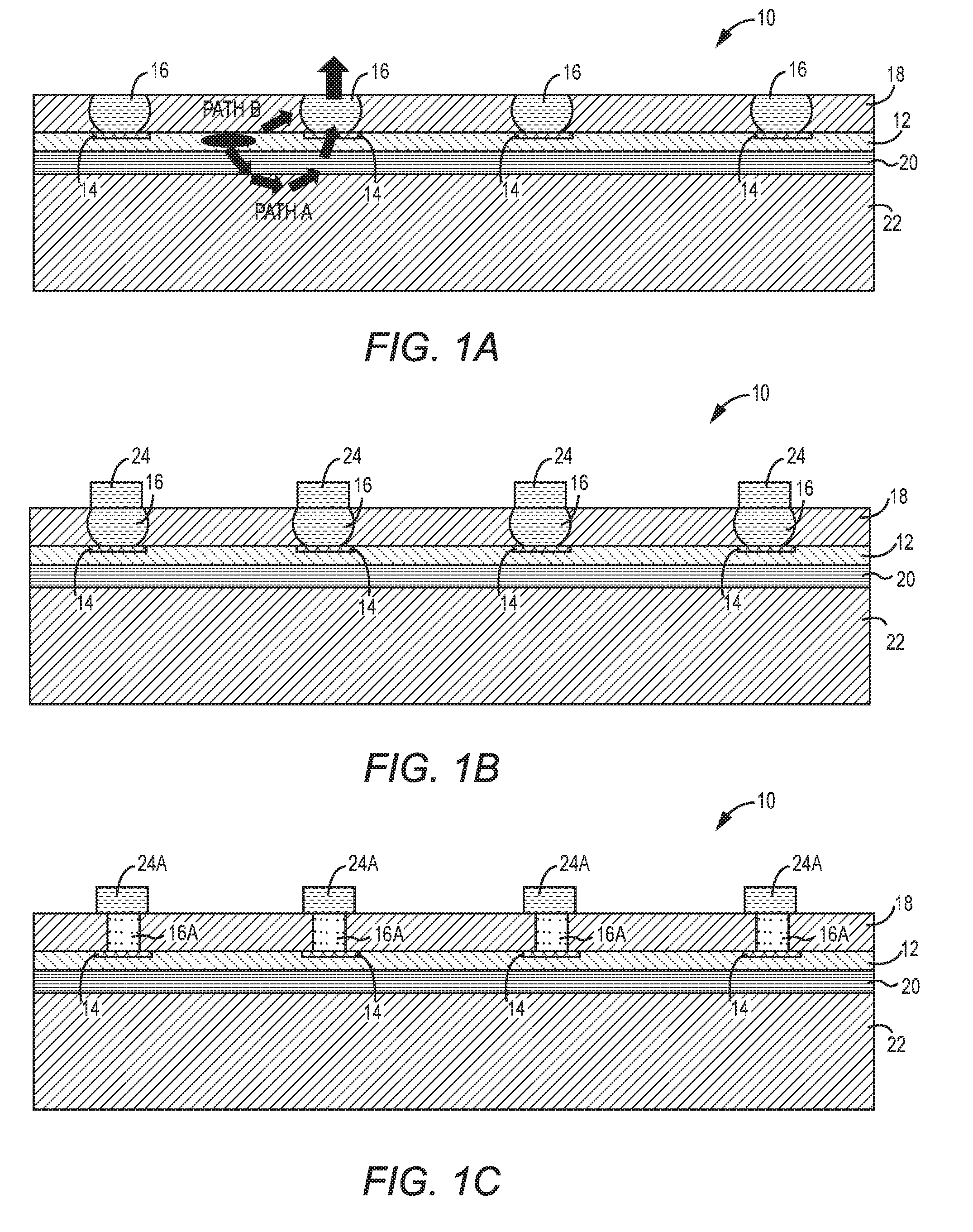
[0045] The present disclosure relates to a mold module with enhanced thermal and electrical performance, and a wafer-level packaging process to provide the mold module with enhanced performance. FIG. 1A shows an exemplary mold module 10 according to one embodiment of the present disclosure. For the purpose of this illustration, the exemplary mold module 10 includes a device layer 12 with a number of input/output (I/O) contacts 14, a number of first bump structures 16, a first mold compound 18, a stop layer 20, and a second mold compound 22.
[0046] In detail, the I/O contacts 14 are located at a top surface of the device layer 12. The device layer 12 may include at least one of a microelectromechanical systems (MEMS) device, an integrated passive device, and an active device (not shown), which may generate heat in the device layer 12. Each first bump structure 16 is formed over the device layer 12 and in contact with a corresponding I/O contact 14. The first mold compound 18 resides over the device layer 12 and partially encapsulates each first bump structure 16, such that a portion of each first bump structure 16 is exposed through the first mold compound 18. The stop layer 20 is formed underneath the device layer 12 and the second mold compound 22 resides underneath the stop layer 20, such that the stop layer 20 separates the device layer 12 from the second mold compound 22.
[0047] The I/O contacts 14 at the top surface of the device layer 12 may be formed of copper, silver, gold or other conductive metals, and the first bump structures 16 are solder balls. As such, each first bump structure 16 and the corresponding I/O contact 14 are electronically coupled. The stop layer 20 may be formed of at least one of silicon oxide or silicon nitride. The heat generated in the device layer 12 may travel through path A and/or path B. For the path A, the heat will travel downward to a top portion of the second mold compound 22, then will pass upward through the stop layer 20, the device layer 12, and the first bump structures 16, which will dissipate the heat. For the path B, the heat will travel directly through the first mold compound 18 to be conducted. It is therefore highly desirable to have high thermal conductivities of both the first and second mold compounds 18 and 22. The first mold compound 18 and the second mold compound 22 may have a thermal conductivity greater than 1 W/mK, or greater than 10 W/mK. In addition, the first mold compound 18 and the second mold compound 22 may have a low dielectric constant less than 7, or between 3 and 5 to yield low radio frequency (RF) coupling between devices (not shown) within the device layer 12. The first mold compound 18 may be formed of a same or different material as the second mold compound 22. The first mold compound 18 may be transparent. In one embodiment, both the first mold compound 18 and the second mold compound 22 may be formed of thermoplastics or thermoset polymer materials, such as PPS (poly phenyl sulfide), overmold epoxies doped with boron nitride or alumina thermal additives, or the like. The device layer has a thickness between 0.1 .mu.m and 50 .mu.m, the stop layer has a thickness between 10 nm and 1000 nm, the first mold compound has a thickness between 10 .mu.m and 1000 .mu.m, and the second mold compound has a thickness between 200 .mu.m and 500 .mu.m.
[0048] Herein, the mold module 10 has a planar top surface, where the first bump structures 16 do not protrude from the top surface of the first mold compound 18. In some applications, it would be desirable to have protruding structures at the top surface of the mold module 10 to facilitate and improve the reliability of die attaching (to the printed circuit board) operations. As shown in FIG. 1B, the mold module 10 may further include a number of second bump structures 24. Each second bump structure 24 is in contact with a corresponding first bump structure 16, and protrudes from the top surface of the first mold compound 18. The second bump structures 24 may be formed from solder paste, such that one I/O contact 14, the corresponding first bump structure 16, and the corresponding second bump structure 24 are electronically coupled. In some applications, the mold module 10 utilizes copper pillars instead of solder balls for first bump structures 16A as illustrated in FIG. 1C. Further, second bump structures 24A may be formed from conductive epoxy or reflowable metals: such as gold, silver, and alloy. Each I/O contact 14, the corresponding first bump structure 16, and the corresponding second bump structure 24 are electronically coupled.
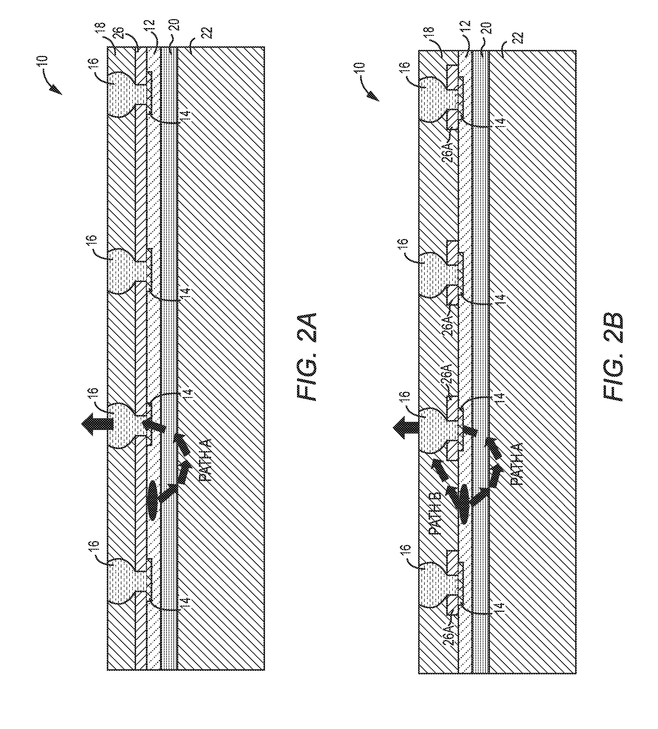
[0049] In another embodiment, the mold module 10 may further include a passivation layer 26 as illustrated in FIG. 2A. The passivation layer 26 is formed over the device layer 12 and a portion of each I/O contact 14 is exposed through the passivation layer 12. Each first bump structure 16 protrudes from a top surface of the passivation layer 26 and is coupled to the exposed portion of the corresponding I/O contact 14 through the passivation layer 26. The first mold compound 18 resides over the passivation layer 26, partially encapsulates each first bump structure 16, and is not in contact with the first mold compound 18. The passivation layer 26 may be formed of benzocyclobutene (BCB) or polyimide, and has a thickness between 5 nm and 5000 nm.
[0050] It is clear to those skilled in the art, this passivation layer 26 may help to mitigate the stresses associated with the module attaching process. However, the passivation layer 26 may have poor thermal conductivity, so as to obstruct the heat generated in the device layer 12 conducting through the first mold compound 18 (no path B). Alternatively, the mold module 10 may include a number of discrete passivation pads 26A instead of the continuous passivation layer 26 formed between the device layer 12 and the first mold compound 18, as illustrated in FIG. 2B. Herein, the discrete passivation pads 26A do not fully cover the device layer 12 and portions of the device layer 12 are in contact with the first mold compound 18. Each I/O contact 14 is aligned underneath a corresponding discrete passivation pad 26A, a portion of each I/O contact 14 is exposed through the corresponding discrete passivation pad 26A, and no I/O contact 14 is in contact with the first mold compound 18. Each first bump structure 16 protrudes from a top surface of the corresponding discrete passivation pad 26A and is coupled to the exposed portion of the corresponding I/O contact 14 through the corresponding discrete passivation pad 26A. The discrete passivation pads 26A may be formed of BCB or polyimide, and each discrete passivation pad 26A has a thickness between 5 nm and 5000 nm.
[0051] Herein, the discrete passivation pads 26A do not separate the device layer 12 from the first mold compound 18. As such, the heat generated in the device layer 12 may travel through path A (from the device layer 12 downward to the top portion of the second mold compound 22, then upward through the stop layer 20, the device layer 12, and the first bump structures 16) and/or path B (from the device layer 12 directly through the first mold compound 18).
[0052] In some applications, the mold module 10 may further include a redistribution structure 28 formed between the device layer 12 and the first mold compound 18, as illustrated in FIG. 3. The redistribution structure 28 includes a first dielectric layer 30, a number of redistribution interconnects 32, and a second dielectric layer 34. The first dielectric layer 30 resides over the device layer 12 and a portion of each I/O contact 14 is exposed through the first dielectric layer 30. Each redistribution interconnect 32 is connected to certain one(s) of the I/O contacts 14 and extends over the first dielectric layer 30. The second dielectric layer 34 resides over the first dielectric layer 30 to partially encapsulate each redistribution interconnect 32, such that a portion of each redistribution interconnect 32 is exposed through the second dielectric layer 34. Each first bump structure 16 protrudes from a top surface of the redistribution structure 28 and is electronically coupled to certain one(s) of the I/O contacts 14 via the redistribution interconnects 32. The first and second dielectric layers 30 and 34 may be formed of BCB or polyimide, and the redistribution interconnects 32 may be formed of copper or other suitable metals. The redistribution structure 28 has a thickness between 2 .mu.m and 300 .mu.m.
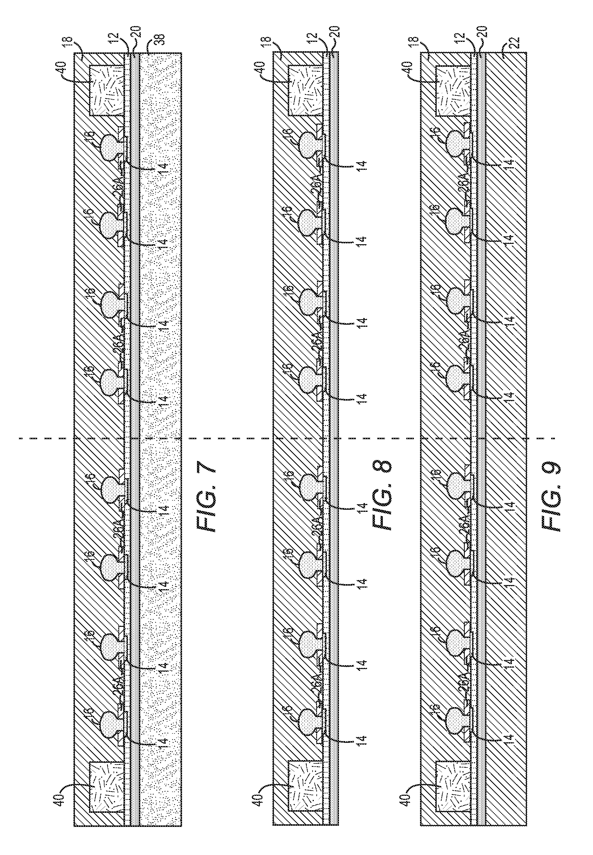
[0053] FIGS. 4-11 provide an exemplary wafer-level packaging process that illustrates steps to fabricate the exemplary mold module 10 shown in FIG. 2B. Although the exemplary steps are illustrated in a series, the exemplary steps are not necessarily order dependent. Some steps may be done in a different order than that presented. Further, processes within the scope of this disclosure may include fewer or more steps than those illustrated in FIGS. 4-11.
[0054] Initially, a precursor wafer 36 is provided as illustrated in FIG. 4. The precursor wafer 36 includes a silicon handle layer 38, the stop layer 20, the device layer 12 with the I/O contacts 14 at the top surface of the device layer 12, the first bump structures 16, and the passivation layer 26. The passivation layer 26 is formed over the device layer 12 and a portion of each I/O contact 14 is exposed through the passivation layer 12. Each first bump structure 16 protrudes from the top surface of the passivation layer 26 and is coupled to the exposed portion of the corresponding I/O contact 14 through the passivation layer 26. The stop layer 20 is formed underneath the device layer 12 and the silicon handle layer 38 resides underneath the stop layer 20, such that the stop layer 20 separates the device layer 12 from the silicon handle layer 38. Herein, the silicon handle layer 38 may have a thickness between 200 .mu.m and 500 .mu.m and a relatively high dielectric constant greater than 7. In some applications, the silicon handle layer 38, the stop layer 20, and the device layer 12 may be formed from a silicon-on-insulator (SOI) structure, which refers to a structure including a silicon substrate, a silicon epitaxy layer, and a buried oxide (BOX) layer sandwiched between the silicon substrate and the silicon epitaxy layer. The silicon handle layer 38 is the silicon substrate of the SOI structure, the stop layer 20 is the BOX layer of the SOI structure, and the device layer 12 is formed from the silicon epitaxy layer of the SOI structure. In some applications, the precursor wafer 36 may not include the passivation layer 26. As such, each first bump structure 16 is formed over the device layer 12 and in contact with a corresponding I/O contact 14.
[0055] The passivation layer 26 is then patterned to form the discrete passivation pads 26A as illustrated in FIG. 5. Herein, the discrete passivation pads 26A do not fully cover the device layer 12. Portions of the device layer 12 are exposed through the discrete passivation pads 26A. Each discrete passivation pad 26A is aligned over a corresponding I/O contact 14, and a portion of each I/O contact 14 is exposed through a corresponding discrete passivation pad 26A. Each first bump structure 16 protrudes from a top surface of the corresponding discrete passivation pad 26A and is coupled to the exposed portion of the corresponding I/O contact 14 through the corresponding discrete passivation pad 26A. Patterning the passivation layer 26 may be provided by a lithography procedure, such as photo masking or stencil screening. If there is no passivation layer 26 included in the precursor wafer 36, the patterning process will be omitted.
[0056] Next, at least one window component 40 may be formed over the device layer 12 at where the wafer mark(s) (not shown) is/are located as illustrated in FIG. 6. Herein, the wafer mark indicates the key location(s) of a wafer, which will be utilized for alignment in a following singulation and/or an assembly process. In one embodiment, the at least one window component 40 is located at the periphery of the device layer 12. The at least one window component 40 may be formed of a transparent material (for instance: transparent silicone material), such that the wafer mark will be seen through the at least one window component 40. In addition, at least one window component 40 may be formed of an easily removable material (for instance: acrylic polymer), such that the wafer mark will be seen after the easy removal of the at least one window component 40 (more details in following discussion). The at least one window component 40 has a height greater than each first bump structure 16 and is not connected to any first bump structure 16. Notice that the at least one window component 40 is optional. In some applications, forming the at least one window component 40 over the device layer 12 may be omitted.
[0057] The first mold compound 18 is applied over the device layer 12 to encapsulate each first bump structure 16 and the at least one window component 40, as illustrated in FIG. 7. The first mold compound 18 may be applied by various procedures, such as compression molding, sheet molding, overmolding, transfer molding, dam fill encapsulation, or screen print encapsulation. The first mold compound 18 may have a superior thermal conductivity greater than 1 W/mK, or greater than 10 W/mK, and may have a dielectric constant less than 7, or between 3 and 5. The first mold compound 18 may resist etching chemistries such as potassium hydroxide (KOH), sodium hydroxide (NaOH), and acetylcholine (ACH). In some applications, the first mold compound 18 may be formed of a transparent material. As such, there is no need to form the at least one window component 40 over the device layer 12, because all locations of a wafer may be seen through the first mold compound 18. A curing process (not shown) is then used to harden the first mold compound 18. The curing temperature is between 100.degree. C. and 320.degree. C. depending on which material is used as the first mold compound 18.
[0058] After the first mold compound 18 is formed, the silicon handle layer 38 is removed substantially as illustrated in FIG. 8. Herein, removing substantially the silicon handle layer 38 refers to removing at least 95% of the entire silicon handle layer 38 and remaining at most 2 .mu.m of the silicon handle layer 38. In desired cases, the silicon handle layer 38 is removed completely, such that the stop layer 20 is exposed. Removing substantially the silicon handle layer 38 may be provided by an chemical mechanical grinding process or an etching process with a wet/dry etchant chemistry, which may be TMAH, KOH, ACH, NaOH, or the like. During the removal process, the first mold compound 18 protects the top surface of the device layer 12, while the stop layer 20 protects a bottom surface of the device layer 12.
[0059] The second mold compound 22 is then applied to an exposed surface from which the silicon handle layer 38 was removed, as illustrated in FIG. 9. If the silicon handle layer 38 is removed completely, the second mold compound 22 is in contact with the stop layer 20. The second mold compound 22 may be applied by various procedures, such as compression molding, sheet molding, overmolding, transfer molding, dam fill encapsulation, and screen print encapsulation. A curing process (not shown) is followed to harden the second mold compound 22. The curing temperature is between 100.degree. C. and 320.degree. C. depending on which material is used as the second mold compound 22. After the curing process, a bottom surface of the second mold compound 22 may be planarized (not shown).
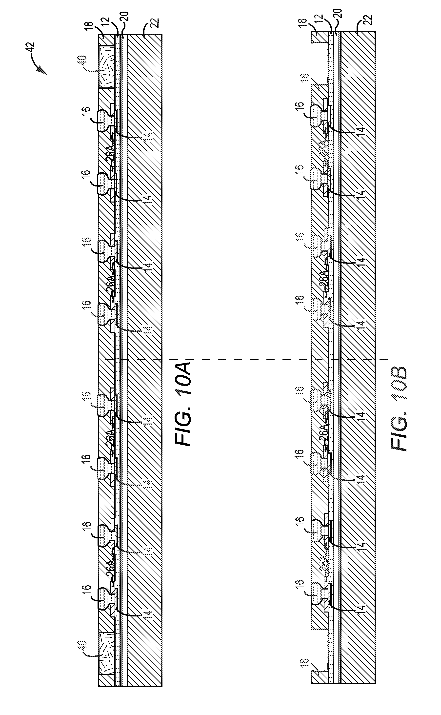
[0060] Next, the first mold compound 18 is thinned down to provide a mold wafer 42 as illustrated in FIG. 10A. Herein, a portion of each first bump structure 16 is exposed. Since the at least one window component 40 has a height greater than each first bump structure 16, a portion of the at least one window component 40 is also exposed through the first mold compound 18. The thinning procedure may be done with a mechanical grinding process. In one embodiment, the at least one window component 40 may be formed of a transparent material, such that the wafer mark indicating the key location(s) of a wafer will be seen through the at least one window component 40. In another embodiment, the at least one window component 40 may be formed of an opaque material, such that the wafer mark indicating the key location(s) of a wafer will not be seen through the at least one window component 40. An extra step to remove the at least one window component 40 is needed, as illustrated in FIG. 10B. After the removal step, at least one portion of the top surface of the device layer 12 is exposed. As such, the wafer mark indicating the key location(s) of a wafer will be seen. Further, in some applications, the second bump structures 24 may be formed after the first mold compound 18 is thinned down, as illustrated in FIG. 10C. Each second bump structure 24 is formed over a corresponding first bump structure 16, and electronically coupled to a corresponding I/O contact 14 via the corresponding first bump structure 16.
[0061] Finally, the mold wafer 42 is singulated into individual mold modules 10, as illustrated in FIG. 11. The singulating step may be provided by a probing and dicing process. The individual mold module 10 may be assembled on the PCB using a number of die attaching methods.
[0062] Those skilled in the art will recognize improvements and modifications to the preferred embodiments of the present disclosure. All such improvements and modifications are considered within the scope of the concepts disclosed herein and the claims that follow.
* * * * *
D00000
D00001
D00002
D00003
D00004
D00005
D00006
D00007
XML
uspto.report is an independent third-party trademark research tool that is not affiliated, endorsed, or sponsored by the United States Patent and Trademark Office (USPTO) or any other governmental organization. The information provided by uspto.report is based on publicly available data at the time of writing and is intended for informational purposes only.
While we strive to provide accurate and up-to-date information, we do not guarantee the accuracy, completeness, reliability, or suitability of the information displayed on this site. The use of this site is at your own risk. Any reliance you place on such information is therefore strictly at your own risk.
All official trademark data, including owner information, should be verified by visiting the official USPTO website at www.uspto.gov. This site is not intended to replace professional legal advice and should not be used as a substitute for consulting with a legal professional who is knowledgeable about trademark law.