Field effect transistor device
Chan , et al. December 31, 2
U.S. patent number 8,618,617 [Application Number 13/783,526] was granted by the patent office on 2013-12-31 for field effect transistor device. This patent grant is currently assigned to GlobalFoundries, Inc., International Business Machines Corporation. The grantee listed for this patent is GlobalFoundries, Inc., International Business Machines Corporation. Invention is credited to Linda R. Black, Kevin K. Chan, Abhishek Dube, Eric C. Harley, Judson R. Holt, Viorel C. Ontalus, Kathryn T. Schonenberg, Matthew W. Stoker, Keith H. Tabakman.


| United States Patent | 8,618,617 |
| Chan , et al. | December 31, 2013 |
Field effect transistor device
Abstract
A method for forming a field effect transistor device includes forming a gate stack portion on a substrate, forming a spacer portion on the gates stack portion and a portion of the substrate, removing an exposed portion of the substrate, epitaxially growing a first silicon material on the exposed portion of the substrate, removing a portion of the epitaxially grown first silicon material to expose a second portion of the substrate, and epitaxially growing a second silicon material on the exposed second portion of the substrate and the first silicon material.
| Inventors: | Chan; Kevin K. (Staten Island, NY), Dube; Abhishek (Fishkill, NY), Harley; Eric C. (Lagrangeville, NY), Holt; Judson R. (Wappingers Falls, NY), Ontalus; Viorel C. (Danbury, CT), Schonenberg; Kathryn T. (Wappingers Falls, NY), Stoker; Matthew W. (Poughkeepsie, NY), Tabakman; Keith H. (Fishkill, NY), Black; Linda R. (Fishkill, NY) | ||||||||||
|---|---|---|---|---|---|---|---|---|---|---|---|
| Applicant: |
|
||||||||||
| Assignee: | International Business Machines
Corporation (Armonk, NY) GlobalFoundries, Inc. (KY) |
||||||||||
| Family ID: | 45351703 | ||||||||||
| Appl. No.: | 13/783,526 | ||||||||||
| Filed: | March 4, 2013 |
Prior Publication Data
| Document Identifier | Publication Date | |
|---|---|---|
| US 20130175547 A1 | Jul 11, 2013 | |
Related U.S. Patent Documents
| Application Number | Filing Date | Patent Number | Issue Date | ||
|---|---|---|---|---|---|
| 12825791 | Jun 29, 2010 | 8492234 | |||
| Current U.S. Class: | 257/401; 257/E21.091; 438/222; 438/300 |
| Current CPC Class: | H01L 29/78618 (20130101); H01L 21/823412 (20130101); H01L 29/66628 (20130101); H01L 21/823481 (20130101); H01L 29/66772 (20130101); H01L 21/823814 (20130101); H01L 21/84 (20130101); H01L 21/823807 (20130101); H01L 29/7848 (20130101); H01L 29/78684 (20130101); H01L 21/823425 (20130101); H01L 21/26586 (20130101) |
| Current International Class: | H01L 27/088 (20060101) |
| Field of Search: | ;257/190,401 |
References Cited [Referenced By]
U.S. Patent Documents
| 6991956 | January 2006 | Ghyselen et al. |
| 7018910 | March 2006 | Ghyselen et al. |
| 7176481 | February 2007 | Chen et al. |
| 7309660 | December 2007 | Chen |
| 7361563 | April 2008 | Shin et al. |
| 7368358 | May 2008 | Ouyang et al. |
| 7396714 | July 2008 | Chen et al. |
| 7402497 | July 2008 | Wei et al. |
| 7456087 | November 2008 | Cheng |
| 7479432 | January 2009 | Murthy et al. |
| 7525161 | April 2009 | Ieong et al. |
| 7572712 | August 2009 | Chong et al. |
| 7622341 | November 2009 | Chudzik et al. |
| 7824993 | November 2010 | Holz et al. |
| 7829421 | November 2010 | Wei et al. |
| 7875521 | January 2011 | Shimamune et al. |
| 7883980 | February 2011 | Grupp et al. |
| 7892932 | February 2011 | Cheng et al. |
| 7910445 | March 2011 | Onoda |
| 7943469 | May 2011 | Cook, Jr. et al. |
| 7964910 | June 2011 | Dyer |
| 7968414 | June 2011 | Ohta et al. |
| 7989298 | August 2011 | Chan et al. |
| 7989901 | August 2011 | Lin et al. |
| 7994014 | August 2011 | Yang et al. |
| 8017487 | September 2011 | Chong et al. |
| 8039341 | October 2011 | Thean et al. |
| 8043919 | October 2011 | Chen et al. |
| 8058133 | November 2011 | Tsai et al. |
| 8062948 | November 2011 | Shin |
| 8071442 | December 2011 | Kronholz et al. |
| 8138050 | March 2012 | Papageorgiou et al. |
| 8154050 | April 2012 | Sudo |
| 8183100 | May 2012 | Mulfinger et al. |
| 8207033 | June 2012 | Kim et al. |
| 8207523 | June 2012 | Tsai et al. |
| 2004/0157409 | August 2004 | Ghyselen et al. |
| 2005/0191825 | September 2005 | Ghyselen et al. |
| 2007/0105331 | May 2007 | Murthy et al. |
| 2007/0254421 | November 2007 | Tsai et al. |
| 2008/0157091 | July 2008 | Shin et al. |
| 2008/0237741 | October 2008 | Ranade et al. |
| 2009/0039399 | February 2009 | Sudo |
| 2009/0124056 | May 2009 | Chen et al. |
| 2009/0140302 | June 2009 | Onoda |
| 2009/0242936 | October 2009 | Cheng et al. |
| 2010/0090289 | April 2010 | Yang et al. |
| 2011/0003450 | January 2011 | Lee et al. |
| 2011/0147828 | June 2011 | Murthy et al. |
| 2011/0183486 | July 2011 | Chan et al. |
| 2011/0254105 | October 2011 | Cheng et al. |
| 2011/0263092 | October 2011 | Cheng et al. |
| 2011/0298008 | December 2011 | Greene et al. |
| 2011/0312145 | December 2011 | Tsai et al. |
| 2011/0316046 | December 2011 | Chan et al. |
Other References
|
Huang, Ru., et al. "Challenges of 22 nm an beyond CMOS technology" Science in China Series F: Information Sciences; vol. 52, No. 9, Sep. 2009. pp. 1491-1533. cited by applicant . Kuppurao, Satheesh, et al., "Integrating Selective Epitaxy in Advanced Logic & Memory Devices", Appliaied Materials, Inc., 2008, 1 pg. cited by applicant . Lee, Minjoo L. et al., "Strained Si, SiGe, and Ge channels for high-mobility metal-oxide-semiconductor field-effect transistors", (c) 2005 American Institute of Physics, downloaded Feb. 11, 2010, see http://jap.aip.org/jp.copyright.jsp; Journal of Applied Physics, 97, 011101 (2005), pp. 97-011101-1-011101-27. cited by applicant . Mistry, K., et al., "Delaying Forever: Uniaxial Strained Silicon Transistors in a 90nm CMOS Technology", Sep. 2004 (c) 2004 IEEE; 2004 Symposium on VLSI Technology, Digest of Technical Papers, pp. 50-51. cited by applicant . Cheng et al., "SiGe-On-Insulator (SGOI): Substrate Preparation and MOSFET Fabrication for Electron Mobility Evaluation", 2001 IEEE International SOI Conference, Oct. 2001, pp. 13-14. cited by applicant . Johnson et al., "Selective Chemical Etching of Polycrystalline SiGe Alloys with Respect to Si and SiO2" Journal of Electronic Materials, vol. 21, No. 8, 1992, pp. 805-810. cited by applicant . Weiser et al., "Nanoscale patterning of Si/SiGe heterostructures by electron-beam lithography and wet-chemical etching" Semicond. Sci. Technol., vol. 15, No. 8, 2000, pp. 862-867. cited by applicant. |
Primary Examiner: Vu; David
Assistant Examiner: Taylor; Earl
Attorney, Agent or Firm: Cantor Colburn LLP Cai; Yuanmin
Parent Case Text
CROSS-REFERENCE TO RELATED APPLICATION
This application is a divisional of U.S. patent application Ser. No. 12/825,791, filed Jun. 29, 2010, the disclosure of which is incorporated by reference herein in its entirety.
Claims
What is claimed is:
1. A field effect transistor device comprising: a gate stack portion disposed on a substrate; a first cavity region in the substrate arranged on a first side of the gate stack portion; a second cavity region in the substrate arranged on a second side of the gate stack portion; a first epitaxially grown silicon material disposed in the first cavity region and the second cavity region, the first epitaxially grown silicon material including a void that exposes a portion of the substrate and defines two stress regions, the two stress regions being separated from one another by a second epitaxially grown silicon material different from the first epitaxially grown material; wherein the two separate stress regions are formed at opposing sides of the void; and the second epitaxially grown silicon material is disposed in the first cavity region and the second cavity region, the second epitaxially grown silicon material in contact with the first epitaxially grown silicon material.
2. The device of claim 1, wherein the first epitaxially grown silicon material defines a planar surface on the first silicon material orientated along a [1,1,1] Miller index axis of the first silicon material.
3. The device of claim 1, wherein the first side of the gate stack portion opposes the second side of the gate stack portion.
4. The device of claim 1, wherein the first epitaxially grown silicon material includes a stress portion defined by the substrate, a channel region of the device, and a planar surface on the first silicon material orientated along a [1,1,1] Miller index axis of the first silicon material.
5. The device of claim 1, wherein the second epitaxially grown silicon material is a doped SiGe material.
6. The device of claim 1, wherein the first epitaxially grown silicon material is a SiGe material including at least 20% by atomic percentage of Ge.
7. The device of claim 1, wherein the first epitaxially grown silicon material is a SiC material.
8. A field effect transistor device comprising: a first gate stack portion disposed on a substrate; a second gate stack portion disposed on the substrate; a cavity region in the substrate arranged between the first gate stack portion and the second gate stack portion; a first epitaxially grown silicon material disposed in the cavity region, the first epitaxially grown silicon material including a void that exposes a portion of the substrate; a first stressor portion disposed in the cavity region adjacent to a channel region of the first gate stack portion; a second stressor portion disposed in the cavity region adjacent to a channel region of the second gate stack portion; wherein the first and second stressor portions are formed at opposing sides of the void; and a doped material disposed in the cavity region on the substrate, the first stressor portion and the second stressor portion, the doped material separating the first stressor portion from the second stressor portion.
9. The device of claim 8, wherein the first and second stressor portions include an epitaxially grown silicon material.
Description
BACKGROUND
The present invention relates to field effect transistor (FET) devices, and more specifically, to methods for fabricating FET devices.
FET devices include source, drain, and channel regions. The source and drain regions include doped ions. The source and drain regions may be doped using ion implantation methods following the formation of the source and drain regions, or may be doped during the formation of the source and drain regions. Stress liner material may be formed proximal to the channel regions. The stress liner material often enhances the carrier mobility and performance of the FET devices.
BRIEF SUMMARY
According to one embodiment of the present invention, a method for forming a field effect transistor device includes forming a gate stack portion on a substrate, forming a spacer portion on the gates stack portion and a portion of the substrate, removing an exposed portion of the substrate, epitaxially growing a first silicon material on the exposed portion of the substrate, removing a portion of the epitaxially grown first silicon material to expose a second portion of the substrate, and epitaxially growing a second silicon material on the exposed second portion of the substrate and the first silicon material.
According to another embodiment of the present invention, a field effect transistor device includes a gate stack portion disposed on a substrate, a first cavity region in the substrate arranged on a first side of the gate stack portion, a second cavity region in the substrate arranged on a second side of the gate stack portion, a first epitaxially grown silicon material disposed in the first cavity region and the second cavity region, and a second epitaxially grown silicon material disposed in the first cavity region and the second cavity region, the second epitaxially grown silicon material in contact with the first epitaxially grown silicon material.
According to yet another embodiment of the present invention, a field effect transistor device includes a first gate stack portion disposed on a substrate, a second gate stack portion disposed on the substrate, a cavity region in the substrate arranged between the first gate stack portion and the second gate stack portion, a first stressor portion disposed in the cavity region adjacent to a channel region of the first gate stack portion, a second stressor portion disposed in the cavity region adjacent to a channel region of the second gate stack portion, and a doped material disposed in the cavity region on the substrate, the first stressor portion and the second stressor portion.
Additional features and advantages are realized through the techniques of the present invention. Other embodiments and aspects of the invention are described in detail herein and are considered a part of the claimed invention. For a better understanding of the invention with the advantages and the features, refer to the description and to the drawings.
BRIEF DESCRIPTION OF THE SEVERAL VIEWS OF THE DRAWINGS
The subject matter which is regarded as the invention is particularly pointed out and distinctly claimed in the claims at the conclusion of the specification. The forgoing and other features, and advantages of the invention are apparent from the following detailed description taken in conjunction with the accompanying drawings in which:
FIGS. 1-7 illustrate side views of a method for forming field effect transistor (FET) devices and the resultant structure of the devices.
FIGS. 8-10 illustrate side views of an alternate method for forming field effect transistor devices and the resultant structure of the devices.
DETAILED DESCRIPTION
FIGS. 1-7 illustrate side view of a method for forming field effect transistor (FET) devices and the resultant structure of the devices. Referring to FIG. 1, gate stacks 102a and 102b, referred to collectively as gate stacks (gate stack portions) 102 hereinafter, are formed on a silicon on insulator (SOI) substrate 100. The gate stacks 102 may include, for example, a dielectric layer 104 such as a high-K layer or oxide layer and a metal layer 106 disposed on the dielectric layer 104. A silicon capping layer 108 is disposed on the metal layer 106. A spacer (spacer portion) 110 is patterned over the gate stacks 102 and a portion of the substrate 100. The spacer 110 may include, for example, a nitride or oxide material. In the illustrated embodiment, the spacer 110 also includes a hardmask portion over the gate stacks 102.
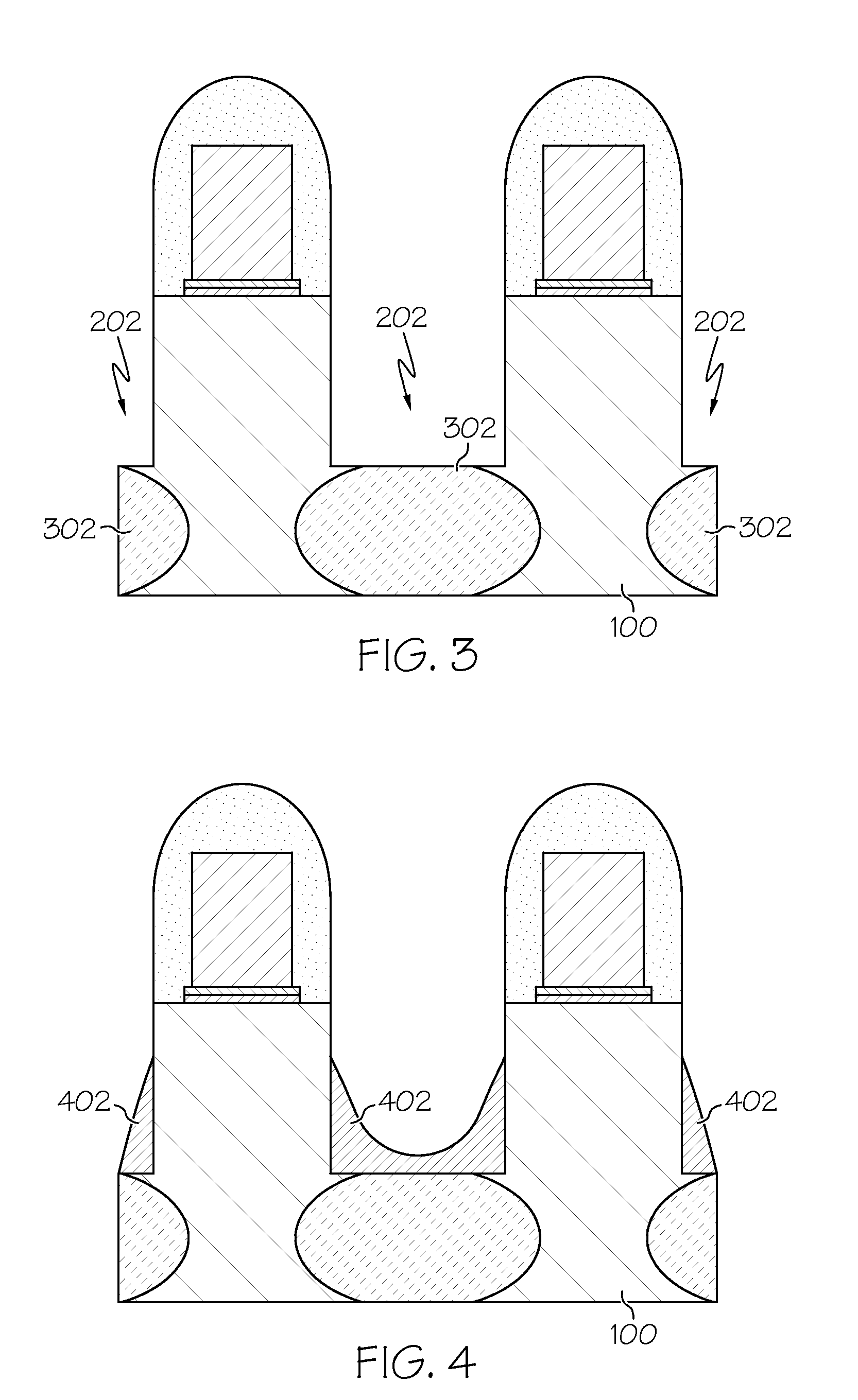
FIG. 2 illustrates the resultant structure following an anisotropic etching process such as, for example, reactive ion etching (RIE) that forms a trench (cavity region) 202 in the substrate 100 between the gate stacks 102a and 102b. Once the trench 202 is formed, the gate stacks 102 that will become n-type (NFET) devices, for example gate stack 102a, may be isolated by patterning a layer of nitride (not shown) over the gate stacks 102, leaving the gate stacks 102 that will become p-type (PFET) devices exposed.
FIG. 3 illustrates regions 302 that may be formed by implanting ions, such as, for example, boron ions, in the substrate 100. In the illustrated embodiment, the regions 302 facilitate isolating adjacent devices such as devices to be formed by gate stacks 102a and 102b. The regions 302 are formed in the substrate 100 below the channels 202, however, in some embodiments, the sidewalls of the channels 202 may also be implanted with ions using, for example, an angled implant process. In alternate embodiments, the regions 302 may not be formed with ion implantation.
FIG. 4 illustrates the resultant structure following the epitaxial growth of a silicon-containing material (epi-silicon) 402 on the exposed portions of the substrate 100. In the illustrated embodiment, the epi-silicon 402 may include, for example, SiGe with greater than 30% (by atomic percentage) Ge content. Alternate embodiments may include between 20-50% Ge content. The epi-silicon 402 material may be undoped, low doped, or counter doped (e.g., doping an n-type region with p-type dopants or doping a p-type region with n-type dopants). In alternate exemplary embodiments, the epi-silicon material 402 may include, for example, SiC or other compound that may be used to form NFET devices. The formation of epi-silicon 402 SiC material includes multiple cycles of epitaxial SiC growth and etching to form the material 402. The carbon (C) content in the epi-silicon SiC may range from approximately 1% to 5%. The epi-silicon SiC may be undoped, low doped (i.e., doped with phosphorous or arsenic) or counter doped.
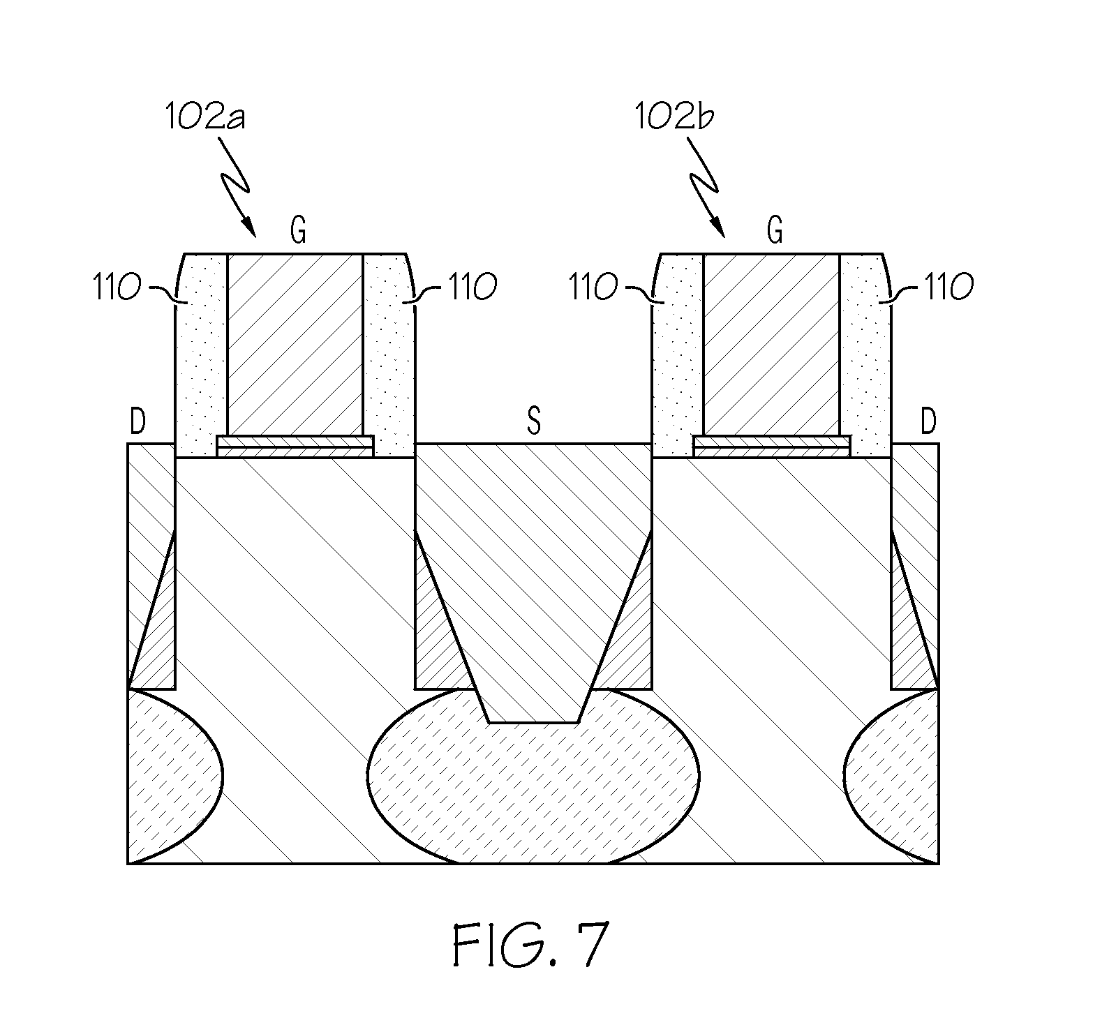
FIG. 5 illustrates the resultant structure following an etching process that removes portions of the epi-silicon material 402. The etching process may include, for example, a hydrogen chlorine (HCl) etch preformed in the epitaxy chamber, or other etching processes such as NH.sub.4OH or Tetramethylammonium Hydroxide (TMAH) wet etching processes. The etching process etches the epi-silicon material 402 at a faster rate than the silicon substrate 100. The crystalline structure of the epi-silicon material 402 and the etching process results in the formation of stress regions 501 partially defined by a plane 500 arranged [1,1,1] (using Miller index notation). The stress regions 501 are adjacent to the channel regions 503 of the devices. The etching process exposes a portion of the substrate 100 in the region 502, between the devices.
FIG. 6 illustrates the resultant structure following the epitaxial growth of doped silicon material 602 that forms the source regions (S) and drain regions (D) of devices 601a and 601b, hereinafter devices 601. In the illustrated embodiment, the doped silicon material 602 includes a doped SiGe material that is epitaxially grown from the exposed substrate 100 and the stress regions 501. The dopant may include, for example boron, arsenic, or phosphorous ions.
FIG. 7 illustrates the resultant structure following the removal of a portion of the spacer 110 that exposes the gate stacks 102a and 102b and defines gate regions (G) of the gate stacks 102. The portion of the spacer material 110 may be removed by, for example, a chemical mechanical polishing process, or a suitable etching process. Once the gate regions (G) have been exposed, a silicide may be formed on the exposed source, gate, and drain regions, and conductive contact material may be formed on the regions (not shown).
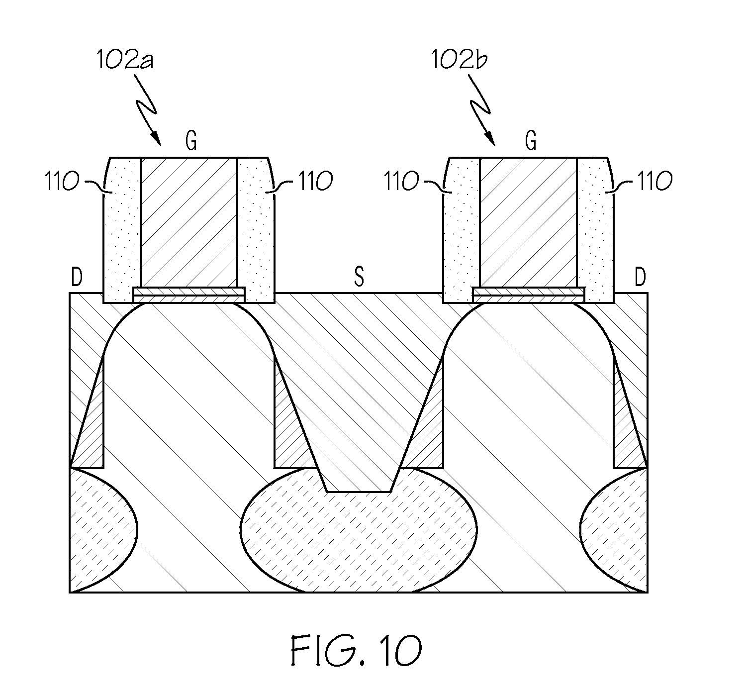
In an alternate embodiment, a similar etching process described above in FIG. 5 may remove portions of the epi-silicon material 402 and the SOI substrate 100. The etching process may include etchant parameters such as etchant chemicals that selectively etch both the epi-silicon material 402 and the silicon substrate 100 material. FIG. 8 illustrates the resulting structure following the removal of portions of the epi-silicon material 402 and the SOI substrate 100 that results in the formation of undercut regions 802. The undercut regions 802 may expose a portion of the gate stacks 102.
FIG. 9 illustrates the resultant structure following the epitaxial growth of doped silicon material 602 that is similar to the process described above in FIG. 6.
FIG. 10 illustrates the resultant structure following the removal of a portion of the spacer 110 that is similar to the process described above in FIG. 7.
The terminology used herein is for the purpose of describing particular embodiments only and is not intended to be limiting of the invention. As used herein, the singular forms "a", "an" and "the" are intended to include the plural forms as well, unless the context clearly indicates otherwise. It will be further understood that the terms "comprises" and/or "comprising," when used in this specification, specify the presence of stated features, integers, steps, operations, elements, and/or components, but do not preclude the presence or addition of one ore more other features, integers, steps, operations, element components, and/or groups thereof.
The corresponding structures, materials, acts, and equivalents of all means or step plus function elements in the claims below are intended to include any structure, material, or act for performing the function in combination with other claimed elements as specifically claimed. The description of the present invention has been presented for purposes of illustration and description, but is not intended to be exhaustive or limited to the invention in the form disclosed. Many modifications and variations will be apparent to those of ordinary skill in the art without departing from the scope and spirit of the invention. The embodiment was chosen and described in order to best explain the principles of the invention and the practical application, and to enable others of ordinary skill in the art to understand the invention for various embodiments with various modifications as are suited to the particular use contemplated
The diagrams depicted herein are just one example. There may be many variations to this diagram or the steps (or operations) described therein without departing from the spirit of the invention. For instance, the steps may be performed in a differing order or steps may be added, deleted or modified. All of these variations are considered a part of the claimed invention.
While the preferred embodiment to the invention had been described, it will be understood that those skilled in the art, both now and in the future, may make various improvements and enhancements which fall within the scope of the claims which follow. These claims should be construed to maintain the proper protection for the invention first described.
* * * * *
References
D00000
D00001
D00002
D00003
D00004
D00005
D00006
XML
uspto.report is an independent third-party trademark research tool that is not affiliated, endorsed, or sponsored by the United States Patent and Trademark Office (USPTO) or any other governmental organization. The information provided by uspto.report is based on publicly available data at the time of writing and is intended for informational purposes only.
While we strive to provide accurate and up-to-date information, we do not guarantee the accuracy, completeness, reliability, or suitability of the information displayed on this site. The use of this site is at your own risk. Any reliance you place on such information is therefore strictly at your own risk.
All official trademark data, including owner information, should be verified by visiting the official USPTO website at www.uspto.gov. This site is not intended to replace professional legal advice and should not be used as a substitute for consulting with a legal professional who is knowledgeable about trademark law.