Cache preload operations using streaming engine
Zbiciak , et al. April 19, 2
U.S. patent number 11,307,858 [Application Number 16/827,875] was granted by the patent office on 2022-04-19 for cache preload operations using streaming engine. This patent grant is currently assigned to TEXAS INSTRUMENTS INCORPORATED. The grantee listed for this patent is TEXAS INSTRUMENTS INCORPORATED. Invention is credited to Timothy David Anderson, Abhijeet Ashok Chachad, Kai Chirca, David M. Thompson, Jonathan (Son) Hung Tran, Daniel Wu, Joseph Raymond Michael Zbiciak.


View All Diagrams
| United States Patent | 11,307,858 |
| Zbiciak , et al. | April 19, 2022 |
Cache preload operations using streaming engine
Abstract
A stream of data is accessed from a memory system using a stream of addresses generated in a first mode of operating a streaming engine in response to executing a first stream instruction. A block cache preload operation is performed on a cache in the memory using a block of addresses generated in a second mode of operating the streaming engine in response to executing a second stream instruction.
| Inventors: | Zbiciak; Joseph Raymond Michael (San Jose, CA), Anderson; Timothy David (University Park, TX), Tran; Jonathan (Son) Hung (Murphy, TX), Chirca; Kai (Dallas, TX), Wu; Daniel (Plano, TX), Chachad; Abhijeet Ashok (Plano, TX), Thompson; David M. (Dallas, TX) | ||||||||||
|---|---|---|---|---|---|---|---|---|---|---|---|
| Applicant: |
|
||||||||||
| Assignee: | TEXAS INSTRUMENTS INCORPORATED
(Dallas, TX) |
||||||||||
| Family ID: | 65809150 | ||||||||||
| Appl. No.: | 16/827,875 | ||||||||||
| Filed: | March 24, 2020 |
Prior Publication Data
| Document Identifier | Publication Date | |
|---|---|---|
| US 20200285470 A1 | Sep 10, 2020 | |
Related U.S. Patent Documents
| Application Number | Filing Date | Patent Number | Issue Date | ||
|---|---|---|---|---|---|
| 16203528 | Nov 28, 2018 | 10606596 | |||
| 15429205 | Feb 10, 2017 | 10162641 | |||
| 14331986 | Mar 28, 2017 | 9606803 | |||
| 61846148 | Jul 15, 2013 | ||||
| Current U.S. Class: | 1/1 |
| Current CPC Class: | G06F 9/3867 (20130101); G06F 12/0897 (20130101); G06F 11/00 (20130101); G06F 9/32 (20130101); G06F 9/30036 (20130101); G06F 12/1036 (20130101); G06F 9/383 (20130101); G06F 9/30098 (20130101); G06F 9/30112 (20130101); G06F 12/0875 (20130101); G06F 12/0862 (20130101); G06F 9/30014 (20130101); G06F 9/3802 (20130101); G06F 9/30145 (20130101); G06F 9/30047 (20130101); G06F 9/3016 (20130101); G06F 9/345 (20130101); G06F 11/1048 (20130101); G06F 11/10 (20130101); G06F 2212/60 (20130101); G06F 2212/6028 (20130101); G06F 9/3822 (20130101); G06F 2212/6022 (20130101); G06F 2212/452 (20130101); G06F 2212/681 (20130101); G06F 2212/1024 (20130101); G06F 2212/657 (20130101) |
| Current International Class: | G06F 9/345 (20180101); G06F 12/0897 (20160101); G06F 9/32 (20180101); G06F 9/38 (20180101); G06F 12/0875 (20160101); G06F 9/30 (20180101); G06F 12/08 (20160101); G06F 11/00 (20060101); G06F 11/10 (20060101); G06F 12/0862 (20160101); G06F 12/1036 (20160101) |
| Field of Search: | ;712/206,207,225,230 ;711/122,171,202,203,206-209,212 |
References Cited [Referenced By]
U.S. Patent Documents
| 5438670 | August 1995 | Baror et al. |
| 6606686 | August 2003 | Agarwala et al. |
| 6665767 | December 2003 | Comisky et al. |
| 6697916 | February 2004 | Lasserre et al. |
| 7185178 | February 2007 | Barreh |
| 7296136 | November 2007 | Collard |
| 7480769 | January 2009 | Diefendorff |
| 7711927 | May 2010 | Sartorius |
| 9904645 | February 2018 | Thompson et al. |
| 2002/0083272 | June 2002 | Matsubara et al. |
| 2002/0156962 | October 2002 | Chopra et al. |
| 2004/0268054 | December 2004 | Peir |
| 2007/0043975 | February 2007 | Varadarajan |
| 2008/0141002 | June 2008 | Bhargava et al. |
| 2012/0137074 | May 2012 | Kim |
| 2013/0232304 | September 2013 | Lohman et al. |
| 2019/0095204 | March 2019 | Zbiciak et al. |
Other References
|
US. Appl. No. 16/825,348 (Year: 2020). cited by examiner . "66AK2Hx Keystone Multicore DSP+ARM System-on-Chips", SPRT651A, Texas Instruments, Inc., 2013, pp. 1-3. cited by applicant. |
Primary Examiner: Pan; Daniel H
Attorney, Agent or Firm: Koch; Charles F. Brill; Charles A. Cimino; Frank D.
Parent Case Text
CROSS-REFERENCE TO RELATED APPLICATIONS
This application is a continuation of U.S. patent application Ser. No. 16/203,528, filed Nov. 28, 2018, which is a continuation in part of U.S. patent application Ser. No. 15/429,205, filed Feb. 10, 2017, now U.S. Pat. No. 10,162,641, which is a division of U.S. patent application Ser. No. 14/331,986, filed Jul. 15, 2014, now U.S. Pat. No. 9,606,803, which claims priority to U.S. Provisional Application No. 61/846,148, filed Jul. 15, 2013, each of which is herein incorporated by reference in its entirety.
Claims
The invention claimed is:
1. A method comprising: receiving an instruction that specifies: a set of data based on a base address and a data size; a level of a cache memory to be preloaded with the set of data; and whether to preload the level of the cache memory with the set of data for a subsequent read or a subsequent write to a set of addresses of the set of data, wherein the subsequent read or the subsequent write occurs after the cache memory has been preloaded with the set of data; determining, based on the base address and the data size, the set of addresses of the set of data; and issuing a set of cache preload operations to the cache memory that includes a cache preload operation for each address in the set of addresses.
2. The method of claim 1, wherein the cache memory includes a level 2 (L2) cache and a level 3 (L3) cache, and the instruction specifies whether to operate on the L2 cache or the L3 cache.
3. The method of claim 1, wherein the cache memory includes a level 1 (L1) cache and a level 2 (L2) cache, and the set of cache preload operations are issued to the L2 cache via a data path that does not include the L1 cache.
4. The method of claim 1 further comprising, when the instruction specifies to preload the level of the cache memory for the subsequent read, the set of cache preload operations request to preload the cache memory in a shared access mode.
5. The method of claim 1 further comprising, when the instruction specifies to preload the level of the cache memory for the subsequent write, the set of cache preload operations request to preload the cache memory in an exclusive access mode.
6. The method of claim 1, wherein the instruction is a first instruction, the method further comprising: asserting an indicator of the set of cache preload operations during the issuing of the set of cache preload operations to the cache memory; and in response to the indicator, causing a processor wait to execute a second instruction.
7. The method of claim 1, wherein: the set of addresses includes a virtual address; the method further comprises translating the virtual address to a physical address; and the issuing of a cache preload operation associated with the virtual address uses the physical address.
8. The method of claim 1 further comprising: determining that an address of the set of addresses is invalid; and notifying a processor that the address is invalid.
9. The method of claim 1 further comprising: determining that an address of the set of addresses causes a page fault; and notifying a processor of the page fault.
10. The method of claim 9 further comprising: saving a state of the set of cache preload operations prior to the page fault; moving a new page of data into the cache memory; and resuming the set of cache preload operations using the saved state.
11. A method comprising: receiving an instruction that specifies a base address, a data size, and a level of a cache memory to operate on; determining, based on the base address and the data size, a set of addresses associated with the instruction; and issuing a set of cache preload operations to the cache memory that includes a cache preload operation for each address in the set of addresses, wherein: the instruction has an associated privilege level; and the method further comprises: for each cache preload operation in the set of cache preload operations, determining whether the privilege level permits preload of the respective address of the cache preload operation; and when the privilege level does not permit preload of a first cache preload operation of the set of cache preload operations, dropping the first cache preload operation while proceeding with a remainder of the set of cache preload operations.
12. A method comprising: receiving an instruction that specifies a base address, a data size, and a level of a cache memory to operate on; determining, based on the base address and the data size, a set of addresses associated with the instruction; issuing a set of cache preload operations to the cache memory that includes a cache preload operation for each address in the set of addresses; determining whether each cache preload operation of the set of cache preload operations is directed to cacheable memory; and when a first cache preload operation of the set of cache preload operations is directed to non-cacheable memory, dropping the first cache preload operation while proceeding with a remainder of the set of cache preload operations.
13. A system comprising: a processor; a memory coupled to the processor that includes a cache memory; and a memory component coupled to the processor and the memory, wherein the memory component is operable to: receive an instruction from the processor that specifies: a set of data; a level of the cache memory to preload with the set of data; and whether to preload the level of the cache memory with the set of data for a subsequent read or a subsequent write to a set of addresses of the set of data, wherein the subsequent read or the subsequent write occurs after the cache memory has been preloaded with the set of data; determine the set of addresses based on the instruction; and issue a set of cache preload operations to the cache memory that includes a cache preload operation for each address in the set of addresses.
14. The system of claim 13, wherein: the instruction further specifies a base address and an amount of data; and the memory component is operable to determine the set of addresses based on the base address and the amount of data.
15. The system of claim 13, wherein the cache memory includes a level 2 (L2) cache and a level 3 (L3) cache, and the instruction specifies whether to operate on the L2 cache or the L3 cache.
16. The system of claim 15, wherein the memory component is coupled to the L2 cache and is operable to issue the set of cache preload operations directly to the L2 cache.
17. The system of claim 13, wherein the memory component is operable to: when the instruction specifies to preload the level of the cache memory for the subsequent read, issue the set of cache preload operations to preload the cache memory in a shared access mode; and when the instruction specifies to preload the level of the cache memory for the subsequent write, issue the set of cache preload operations to preload the cache memory in an exclusive access mode.
18. The system of claim 13, wherein the memory component is operable to: determine whether each cache preload operation of the set of cache preload operations is directed to cacheable memory; and when a first cache preload operation of the set of cache preload operations is directed to non-cacheable memory, drop the first cache preload operation while proceeding with a remainder of the set of cache preload operations.
19. The system of claim 13, wherein the memory component is further operable to: detect that a first address of the set of addresses is associated with a page fault; in response to the page fault, save a current state of the set of cache preload operations; and resume the set of cache preload operations using the current state after the page fault is resolved.
20. The system of claim 19, wherein the memory component is further operable to, in response to the page fault, notifying the processor of the page fault.
Description
TECHNICAL FIELD
This relates to using a streaming engine to perform block-oriented cache preloading.
BACKGROUND
Digital signal processors (DSP) are optimized for processing streams of data that may be derived from various input signals, such as sensor data, a video stream, a voice channel, radar signals, biomedical signals, etc. Digital signal processors operating on real-time data typically receive an input data stream, perform a filter function on the data stream (such as encoding or decoding) and output a transformed data stream. The system is called real-time because the application fails if the transformed data stream is not available for output when scheduled. Typical video encoding requires a predictable but non-sequential input data pattern. A typical application requires memory access to load data registers in a data register file and then supply data from the data registers to functional units which perform the data processing.
One or more DSP processing cores can be combined with various peripheral circuits, blocks of memory, etc. on a single integrated circuit (IC) die to form a system on chip (SoC). These systems can include multiple interconnected processors that share the use of on-chip and off-chip memory. A processor can include some combination of instruction cache (ICache) and data cache (DCache) to improve processing. Furthermore, multiple processors with shared memory can be incorporated in a single embedded system. The processors can physically share the same memory without accessing data or executing code located in the same memory locations or can use some portion of the shared memory as common shared memory.
SUMMARY
Methods and apparatus are provided such that a stream of data can be accessed from a memory system using a first stream of addresses generated in a first mode of operating a streaming engine in response to executing a first stream instruction. A block cache preload operation can be performed on a cache in the memory system using a second stream of addresses generated in a second mode of operating the streaming engine in response to executing a second stream instruction.
BRIEF DESCRIPTION OF THE DRAWINGS
FIG. 1 illustrates an example dual scalar/vector data path processor.
FIG. 2 illustrates the registers and functional units in the dual scalar/vector data path processor illustrated in FIG. 1.
FIG. 3 illustrates a global scalar register file.
FIG. 4 illustrates a local scalar register file shared by arithmetic functional units.
FIG. 5 illustrates a local scalar register file shared by multiply functional units.
FIG. 6 illustrates a local scalar register file shared by load/store units.
FIG. 7 illustrates a global vector register file.
FIG. 8 illustrates a predicate register file.
FIG. 9 illustrates a local vector register file shared by arithmetic functional units.
FIG. 10 illustrates a local vector register file shared by multiply and correlation functional units.
FIG. 11 illustrates pipeline phases of a processing unit.
FIG. 12 illustrates sixteen instructions of a single fetch packet.
FIG. 13 illustrates an example of the instruction coding of instructions.
FIG. 14 illustrates bit coding of a condition code extension slot 0.
FIG. 15 illustrates bit coding of a condition code extension slot 1.
FIG. 16 illustrates bit coding of a constant extension slot 0.
FIG. 17 is a partial block diagram illustrating constant extension.
FIG. 18 illustrates carry control for SIMD operations.
FIG. 19 illustrates a conceptual view of streaming engines.
FIG. 20 illustrates a sequence of formatting operations.
FIG. 21 illustrates an example of lane allocation in a vector.
FIG. 22 illustrates an example of lane allocation in a vector.
FIG. 23 illustrates a basic two-dimensional (2D) stream.
FIG. 24 illustrates the order of elements within the example stream of FIG. 23.
FIG. 25 illustrates extracting a smaller rectangle from a larger rectangle.
FIG. 26 illustrates how an example streaming engine fetches a stream with a transposition granularity of 4 bytes.
FIG. 27 illustrates how an example streaming engine fetches a stream with a transposition granularity of 8 bytes.
FIG. 28 illustrates the details of an example streaming engine.
FIG. 29 illustrates an example stream template register.
FIG. 30 illustrates sub-field definitions of the flags field of the example stream template register of FIG. 29.
FIG. 31 illustrates an example of a vector length masking/group duplication block.
FIG. 32 is a partial schematic diagram of an example of the generation of the stream engine valid or invalid indication.
FIG. 33 is a partial schematic diagram of a streaming engine address generator illustrating generation of the loop address and loop count.
FIG. 34 illustrates a partial schematic diagram showing the streaming engine supply of data of this example.
FIG. 35 illustrates a partial schematic diagram showing the streaming engine supply of valid data to the predicate unit.
FIG. 36 is a block diagram of a multiprocessor system with multiple levels of cache.
FIG. 37 is a partial schematic diagram for cache management operations using the streaming engine of FIG. 28.
FIG. 38 is a flow chart illustrating operation of cache management operations using the streaming engine.
DETAILED DESCRIPTION
In the drawings, like elements are denoted by like reference numerals for consistency.
Digital signal processors (DSP) are optimized for processing streams of data that may be derived from various input signals, such as sensor data, a video stream, a voice channel, radar signals, biomedical signals, etc. Memory bandwidth and scheduling are concerns for digital signal processors operating on real-time data. An example DSP processing core is described herein that includes a streaming engine to improve memory bandwidth and data scheduling.
One or more DSP processing cores can be combined with various peripheral circuits, blocks of memory, etc. on a single integrated circuit (IC) die to form a system on chip (SoC). See, for example, "66AK2Hx Multicore Keystone.TM. DSP+ARM.RTM. System-on-Chip," 2013 which is incorporated by reference herein.
In the example DSP core described herein, an autonomous streaming engine (SE) is coupled to the DSP. In this example, the streaming engine includes two closely coupled streaming engines that can manage two data streams simultaneously. In another example, the streaming engine is capable of managing only a single stream, while in other examples the streaming engine is capable of handling more than two streams. In each case, for each stream, the streaming engine includes an address generation stage, a data formatting stage, and some storage for formatted data waiting for consumption by the processor. In the examples described herein, addresses are derived from algorithms that can involve multi-dimensional loops, each dimension maintaining an iteration count. In one example, the streaming engine supports six levels of nested iteration. In other examples, more or fewer levels of iteration are supported.
In this example, the DSP data processing systems employs data caches and instruction caches to improve performance. A small amount of high-speed memory is used for each cache. These cache memories are filled from main memory on an as-needed basis. When the data processor requires data or an instruction, this is first sought from the respective cache memory. If the data or instruction sought is already stored in the cache memory, it is recalled faster than it could have been recalled from main memory. If the data or instruction sought is not stored in the cache memory, it is recalled from main memory for use and stored in the corresponding cache. A performance improvement is achieved using cache memory based upon the principle of locality of reference. It is likely that the data or the instruction just sought by the data processor will be needed again soon. Use of cache memories speeds the accesses needed to service these future needs.
It is desirable to provide a level of control to the programmer over cache operations. In this example, the cache system supports a writeback mechanism, whereby the programmer can direct the cache to write data in the cache back to external memory for shared access by another processor which doesn't have access to the cache. Similarly, it is often desirable to be able to clear or invalidate cache entries so that new data can be accessed at addresses which have been updated in the reference memory. In some applications it is desirable to be able to preload data into a selected hierarchical level of cache in order to assure that the data is available when accessed by a program.
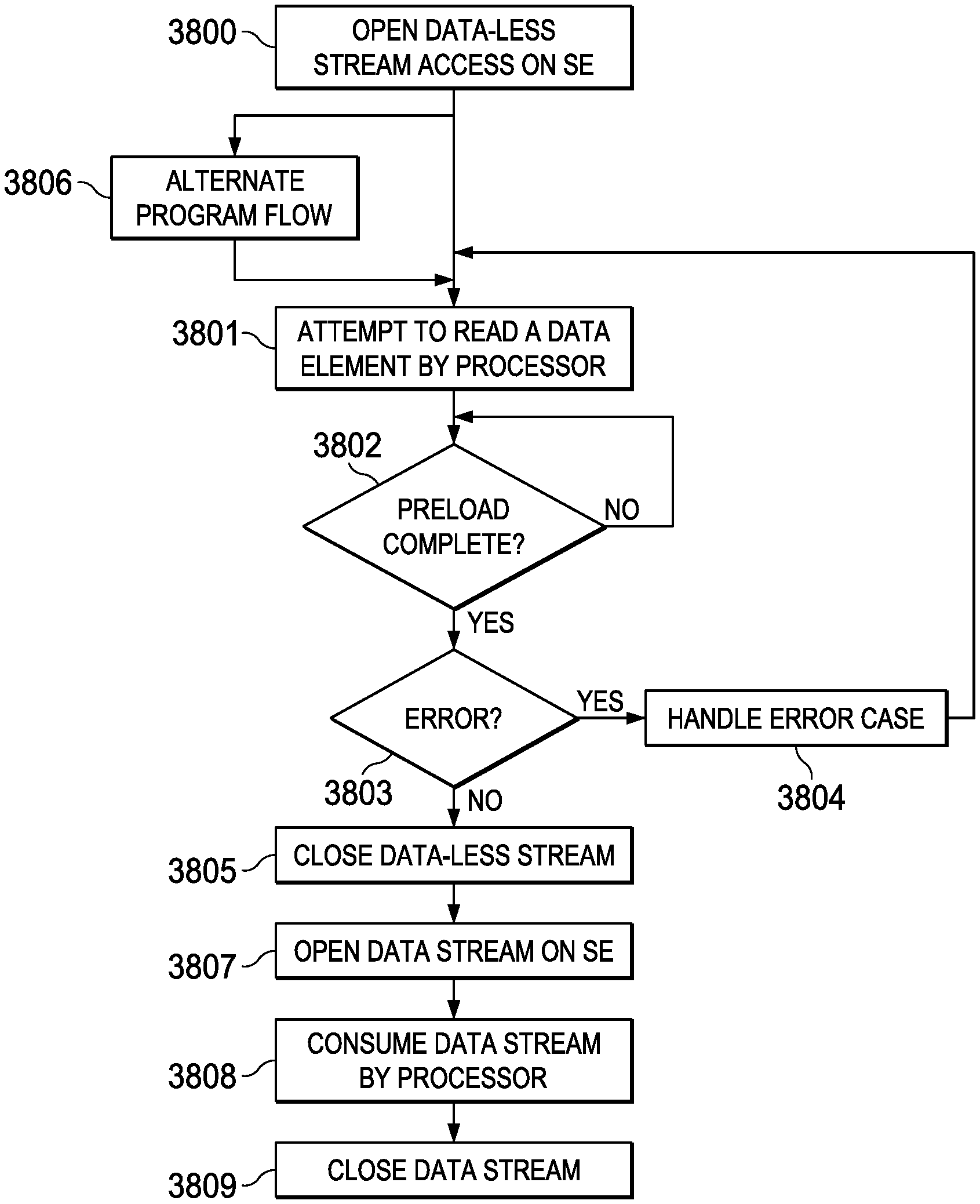
In this example, in addition to its core data stream support, the streaming engine supports a range of special "data-less" streams. A data-less stream may be used move data between various levels of cache and memory, without bringing data to the processor. In this example, two special instructions are provided to allow a program to initiate a data-less stream. A block cache maintenance operation is initiated by a "BLKCMO" instruction. A block cache preload operation is initiated with a "BLKPLD" instruction.
An example of performing block-oriented cache maintenance operations and block oriented cache preloading using BLKCMO and BLKPLD instructions is described in more detail with regard to FIGS. 36-38.
An example DSP processor is described in detail herein with reference to FIGS. 1-18. An example streaming engine capable of managing two data streams using six-dimensional nested loops is described in detail herein with reference to FIGS. 19-35.
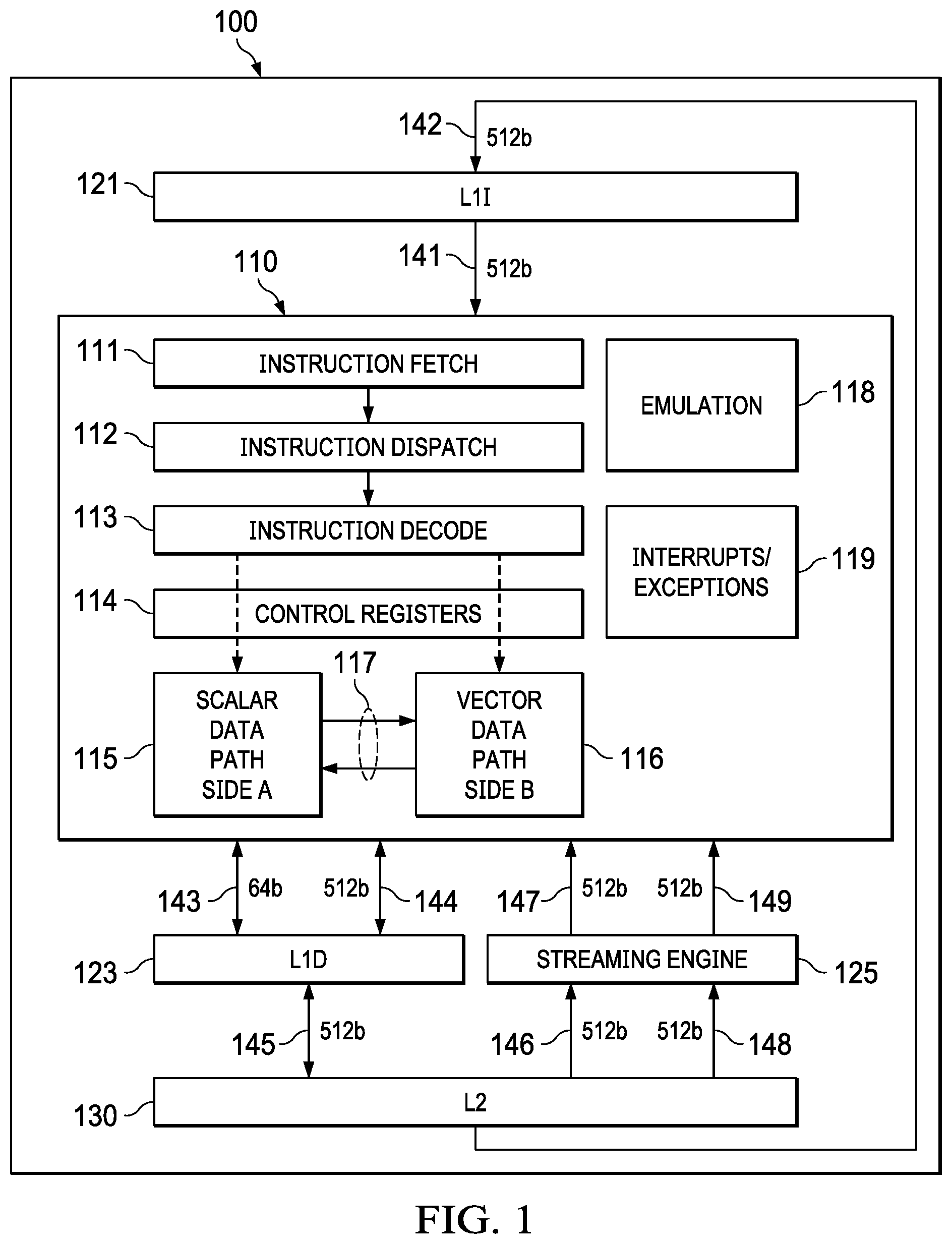
FIG. 1 illustrates an example processor 100 that includes dual scalar/vector data paths 115, 117. Processor 100 includes a streaming engine 125 that is described in more detail herein. Processor 100 includes separate level one instruction cache (L1D) 121 and level one data cache (L1D) 123. Processor 100 includes a level 2 (L2) combined instruction/data cache 130 that holds both instructions and data. FIG. 1 illustrates connection between L1I cache and L2 combined instruction/data cache 130, 512-bit bus 142. FIG. 1 illustrates the connection between L1D cache 123 and L2 combined instruction/data cache 130, 512-bit bus 145. In the example processor 100, L2 combined instruction/data cache 130 stores both instructions to back up L1I cache 121 and data to back up L1D cache 123. In this example, L2 combined instruction/data cache 130 is further connected to higher level cache and/or main memory using known or later developed memory system techniques not illustrated in FIG. 1. As used herein, the term "higher level" memory or cache refers to a next level in a memory hierarchy that is more distant from the processor, while the term "lower level" memory or cache refers to a level in the memory hierarchy that is closer to the processor. L1I cache 121, L1D cache 123, and L2 cache 130 may be implemented in different sizes in various examples. In this example, L1I cache 121 and L1D cache 123 are each 32K bytes, and L2 cache 130 is 1024K bytes. In the example processor 100, L1I cache 121, L1D cache 123 and L2 combined instruction/data cache 130 are formed on a single integrated circuit. This single integrated circuit optionally includes other circuits.
Processing unit core 110 fetches instructions from L1I cache 121 as controlled by instruction fetch unit 111. Instruction fetch unit 111 determines the next instructions to be executed and recalls a fetch packet sized set of such instructions. The nature and size of fetch packets are further detailed below. Instructions are directly fetched from L1I cache 121 upon a cache hit if the instructions are stored in L1I cache 121. Upon a cache miss occurring when the specified instructions are not stored in L1I cache 121, the instructions are sought in L2 combined cache 130. In this example, the size of a cache line in L1I cache 121 equals the size of a fetch packet which is 512 bits. The memory locations of these instructions are either a hit in L2 combined cache 130 or a miss. A hit is serviced from L2 combined cache 130. A miss is serviced from a higher level of cache (not illustrated) or from main memory (not illustrated). In this example, the requested instruction is simultaneously supplied to both L1I cache 121 and processing unit core 110 to speed use.
In this example, processing unit core 110 includes multiple functional units to perform instruction specified data processing tasks. Instruction dispatch unit 112 determines the target functional unit of each fetched instruction. In this example, processing unit 110 operates as a very long instruction word (VLIW) processor capable of operating on multiple instructions in corresponding functional units simultaneously. A complier organizes instructions in execute packets that are executed together. Instruction dispatch unit 112 directs each instruction to its target functional unit. The functional unit assigned to an instruction is completely specified by the instruction produced by the compiler. The hardware of processing unit core 110 has no part in the functional unit assignment. In this example, instruction dispatch unit 112 operates on several instructions in parallel. The number of such parallel instructions is set by the size of the execute packet. This is further described herein.
One part of the dispatch task of instruction dispatch unit 112 is determining whether the instruction is to execute on a functional unit in scalar data path side A 115 or vector data path side B 116. An instruction bit within each instruction called the s bit determines which data path the instruction controls. This is further described herein.
Instruction decode unit 113 decodes each instruction in a current execute packet. Decoding includes identification of the functional unit performing the instruction, identification of registers used to supply data for the corresponding data processing operation from among possible register files, and identification of the register destination of the results of the corresponding data processing operation. As further explained below, instructions can include a constant field in place of one register number operand field. The result of this decoding are signals for control of the target functional unit to perform the data processing operation specified by the corresponding instruction on the specified data.
Processing unit core 110 includes control registers 114. Control registers 114 store information for control of the functional units in scalar data path side A 115 and vector data path side B 116. This information may include mode information or the like.
The decoded instructions from instruction decode 113 and information stored in control registers 114 are supplied to scalar data path side A 115 and vector data path side B 116. As a result, functional units within scalar data path side A 115 and vector data path side B 116 perform instruction specified data processing operations upon instruction specified data and store the results in an instruction specified data register or registers. Each of scalar data path side A 115 and vector data path side B 116 include multiple functional units that operate in parallel. These are further described below in conjunction with FIG. 2. There is a data path 117 between scalar data path side A 115 and vector data path side B 116 permitting data exchange.
Processing unit core 110 includes further non-instruction-based modules. Emulation unit 118 permits determination of the machine state of processing unit core 110 in response to instructions. This capability can be employed for algorithmic development. Interrupts/exceptions unit 119 enables processing unit core 110 to be responsive to external, asynchronous events (interrupts) and to respond to attempts to perform improper operations (exceptions).
Processor 100 includes streaming engine 125. Streaming engine 125 supplies two data streams from predetermined addresses cached in L2 combined cache 130 to register files of vector data path side B of processing unit core 110. This provides controlled data movement from memory (as cached in L2 combined cache 130) directly to functional unit operand inputs. This is further described herein.
FIG. 1 illustrates example data widths of busses between various parts. L1I cache 121 supplies instructions to instruction fetch unit 111 via bus 141. Bus 141 is a 512-bit bus in this example. Bus 141 is unidirectional from L1I cache 121 to processing unit 110. L2 combined cache 130 supplies instructions to L1I cache 121 via bus 142. Bus 142 is a 512-bit bus in this example. Bus 142 is unidirectional from L2 combined cache 130 to L1I cache 121.
L1D cache 123 exchanges data with register files in scalar data path side A 115 via bus 143. Bus 143 is a 64-bit bus in this example. L1D cache 123 exchanges data with register files in vector data path side B 116 via bus 144. Bus 144 is a 512-bit bus in this example. Busses 143 and 144 are illustrated as bidirectional supporting both processing unit core 110 data reads and data writes. L1D cache 123 exchanges data with L2 combined cache 130 via bus 145. Bus 145 is a 512-bit bus in this example. Bus 145 is illustrated as bidirectional supporting cache service for both processing unit core 110 data reads and data writes.
Processor data requests are directly fetched from L1D cache 123 upon a cache hit (if the requested data is stored in L1D cache 123). Upon a cache miss (the specified data is not stored in L1D cache 123), the data is sought in L2 combined cache 130. The memory locations of the requested data are either a hit in L2 combined cache 130 or a miss. A hit is serviced from L2 combined cache 130. A miss is serviced from another level of cache (not illustrated) or from main memory (not illustrated). The requested data may be simultaneously supplied to both L1D cache 123 and processing unit core 110 to speed use.
L2 combined cache 130 supplies data of a first data stream to streaming engine 125 via bus 146. Bus 146 is a 512-bit bus in this example. Streaming engine 125 supplies data of the first data stream to functional units of vector data path side B 116 via bus 147. Bus 147 is a 512-bit bus in this example. L2 combined cache 130 supplies data of a second data stream to streaming engine 125 via bus 148. Bus 148 is a 512-bit bus in this example. Streaming engine 125 supplies data of this second data stream to functional units of vector data path side B 116 via bus 149, which is a 512-bit bus in this example. Busses 146, 147, 148 and 149 are illustrated as unidirectional from L2 combined cache 130 to streaming engine 125 and to vector data path side B 116 in accordance with this example.
Streaming engine data requests are directly fetched from L2 combined cache 130 upon a cache hit (if the requested data is stored in L2 combined cache 130). Upon a cache miss (the specified data is not stored in L2 combined cache 130), the data is sought from another level of cache (not illustrated) or from main memory (not illustrated). It is technically feasible in some examples for L1D cache 123 to cache data not stored in L2 combined cache 130. If such operation is supported, then upon a streaming engine data request that is a miss in L2 combined cache 130, L2 combined cache 130 snoops L1D cache 123 for the stream engine requested data. If L1D cache 123 stores the data, the snoop response includes the data, which is then supplied to service the streaming engine request. If L1D cache 123 does not store the data, the snoop response indicates this and L2 combined cache 130 services the streaming engine request from another level of cache (not illustrated) or from main memory (not illustrated).
In this example, both L1D cache 123 and L2 combined cache 130 can be configured as selected amounts of cache or directly addressable memory in accordance with U.S. Pat. No. 6,606,686 entitled UNIFIED MEMORY SYSTEM ARCHITECTURE INCLUDING CACHE AND DIRECTLY ADDRESSABLE STATIC RANDOM ACCESS MEMORY, which is incorporated by reference herein.
In this example, processor 100 is fabricated on an integrated chip (IC) that is mounted on a ball grid array (BGA) substrate. A BGA substrate and IC die together may be referred to as "BGA package," "IC package," "integrated circuit," "IC," "chip," "microelectronic device," or similar terminology. The BGA package may include encapsulation material to cover and protect the IC die from damage. In another example, other types of known or later developed packaging techniques may be used with processor 100.
FIG. 2 illustrates further details of functional units and register files within scalar data path side A 115 and vector data path side B 116. Scalar data path side A 115 includes L1 unit 221, S1 unit 222, M1 unit 223, N1 unit 224, D1 unit 225 and D2 unit 226. Scalar data path side A 115 includes global scalar register file 211, L1/S1 local register file 212, M1/N1 local register file 213 and D1/D2 local register file 214. Vector data path side B 116 includes L2 unit 241, S2 unit 242, M2 unit 243, N2 unit 244, C unit 245 and P unit 246. Vector data path side B 116 includes global vector register file 231, L2/S2 local register file 232, M2/N2/C local register file 233 and predicate register file 234. Which functional units can read from or write to which register files is described in more detail herein.
Scalar data path side A 115 includes L1 unit 221. L1 unit 221 generally accepts two 64-bit operands and produces one 64-bit result. The two operands are each recalled from an instruction specified register in either global scalar register file 211 or L1/S1 local register file 212. L1 unit 221 performs the following instruction selected operations: 64-bit add/subtract operations; 32-bit min/max operations; 8-bit Single Instruction Multiple Data (SIMD) instructions such as sum of absolute value, minimum and maximum determinations; circular min/max operations; and various move operations between register files. The result is written into an instruction specified register of global scalar register file 211, L1/S1 local register file 212, M1/N1 local register file 213 or D1/D2 local register file 214.
Scalar data path side A 115 includes S1 unit 222. S1 unit 222 generally accepts two 64-bit operands and produces one 64-bit result. The two operands are each recalled from an instruction specified register in either global scalar register file 211 or L1/S1 local register file 212. In this example, S1 unit 222 performs the same type operations as L1 unit 221. In another example, there may be slight variations between the data processing operations supported by L1 unit 221 and S1 unit 222. The result is written into an instruction specified register of global scalar register file 211, L1/S1 local register file 212, M1/N1 local register file 213 or D1/D2 local register file 214.
Scalar data path side A 115 includes M1 unit 223. M1 unit 223 generally accepts two 64-bit operands and produces one 64-bit result. The two operands are each recalled from an instruction specified register in either global scalar register file 211 or M1/N1 local register file 213. In this example, M1 unit 223 performs the following instruction selected operations: 8-bit multiply operations; complex dot product operations; 32-bit bit count operations; complex conjugate multiply operations; and bit-wise Logical Operations, moves, adds and subtracts. The result is written into an instruction specified register of global scalar register file 211, L1/S1 local register file 212, M1/N1 local register file 213 or D1/D2 local register file 214.
Scalar data path side A 115 includes N1 unit 224. N1 unit 224 generally accepts two 64-bit operands and produces one 64-bit result. The two operands are each recalled from an instruction specified register in either global scalar register file 211 or M1/N1 local register file 213. In this example, N1 unit 224 performs the same type operations as M1 unit 223. There are also double operations (called dual issued instructions) that employ both the M1 unit 223 and the N1 unit 224 together. The result is written into an instruction specified register of global scalar register file 211, L1/S1 local register file 212, M1/N1 local register file 213 or D1/D2 local register file 214.
Scalar data path side A 115 includes D1 unit 225 and D2 unit 226. D1 unit 225 and D2 unit 226 generally each accept two 64-bit operands and each produce one 64-bit result. D1 unit 225 and D2 unit 226 generally perform address calculations and corresponding load and store operations. D1 unit 225 is used for scalar loads and stores of 64 bits. D2 unit 226 is used for vector loads and stores of 512 bits. In this example, D1 unit 225 and D2 unit 226 also perform: swapping, pack and unpack on the load and store data; 64-bit SIMD arithmetic operations; and 64-bit bit-wise logical operations. D1/D2 local register file 214 stores base and offset addresses used in address calculations for the corresponding loads and stores. The two operands are each recalled from an instruction specified register in either global scalar register file 211 or D1/D2 local register file 214. The calculated result is written into an instruction specified register of global scalar register file 211, L1/S1 local register file 212, M1/N1 local register file 213 or D1/D2 local register file 214.
Vector data path side B 116 includes L2 unit 241. L2 unit 241 generally accepts two 512-bit operands and produces one 512-bit result. The two operands are each recalled from an instruction specified register in either global vector register file 231, L2/S2 local register file 232 or predicate register file 234. In this example, L2 unit 241 performs instruction similar to L1 unit 221 except on wider 512-bit data. The result may be written into an instruction specified register of global vector register file 231, L2/S2 local register file 232, M2/N2/C local register file 233 or predicate register file 234.
Vector data path side B 116 includes S2 unit 242. S2 unit 242 generally accepts two 512-bit operands and produces one 512-bit result. The two operands are each recalled from an instruction specified register in either global vector register file 231, L2/S2 local register file 232 or predicate register file 234. In this example, S2 unit 242 performs instructions similar to S1 unit 222. The result is written into an instruction specified register of global vector register file 231, L2/S2 local register file 232, M2/N2/C local register file 233 or predicate register file 234.
Vector data path side B 116 includes M2 unit 243. M2 unit 243 generally accepts two 512-bit operands and produces one 512-bit result. The two operands are each recalled from an instruction specified register in either global vector register file 231 or M2/N2/C local register file 233. In this example, M2 unit 243 performs instructions similar to M1 unit 223 except on wider 512-bit data. The result is written into an instruction specified register of global vector register file 231, L2/S2 local register file 232 or M2/N2/C local register file 233.
Vector data path side B 116 includes N2 unit 244. N2 unit 244 generally accepts two 512-bit operands and produces one 512-bit result. The two operands are each recalled from an instruction specified register in either global vector register file 231 or M2/N2/C local register file 233. In this example, N2 unit 244 performs the same type operations as M2 unit 243. There are also double operations (called dual issued instructions) that employ both M2 unit 243 and the N2 unit 244 together. The result is written into an instruction specified register of global vector register file 231, L2/S2 local register file 232 or M2/N2/C local register file 233.
Vector data path side B 116 includes correlation (C) unit 245. C unit 245 generally accepts two 512-bit operands and produces one 512-bit result. The two operands are each recalled from an instruction specified register in either global vector register file 231 or M2/N2/C local register file 233. In this example, C unit 245 performs "Rake" and "Search" instructions that are used for WCDMA (wideband code division multiple access) encoding/decoding. In this example, C unit 245 can perform up to 512 multiples per clock cycle of a 2-bit PN (pseudorandom number) and 8-bit I/Q (complex number), 8-bit and 16-bit Sum-of-Absolute-Difference (SAD) calculations, up to 512 SADs per clock cycle, horizontal add and horizontal min/max instructions, and vector permutes instructions. C unit 245 also contains 4 vector control registers (CUCR0 to CUCR3) used to control certain operations of C unit 245 instructions. Control registers CUCR0 to CUCR3 are used as operands in certain C unit 245 operations. In some examples, control registers CUCR0 to CUCR3 are used in control of a general permutation instruction (VPERM), and as masks for SIMD multiple DOT product operations (DOTPM) and SIMD multiple Sum-of-Absolute-Difference (SAD) operations. In further examples, control register CUCR0 is used to store the polynomials for Galois Field Multiply operations (GFMPY) and control register CUCR1 is used to store the Galois field polynomial generator function.
Vector data path side B 116 includes P unit 246. Vector predicate (P) unit 246 performs basic logic operations on registers of local predicate register file 234. P unit 246 has direct access to read from and write to predication register file 234. The logic operations include single register unary operations such as NEG (negate) which inverts each bit of the single register, BITCNT (bit count) which returns a count of the number of bits in the single register having a predetermined digital state (1 or 0), RMBD (right most bit detect) which returns a number of bit positions from the least significant bit position (right most) to a first bit position having a predetermined digital state (1 or 0), DECIMATE which selects every instruction specified Nth (1, 2, 4, etc.) bit to output, and EXPAND which replicates each bit an instruction specified N times (2, 4, etc.). The logic operations also include two register binary operations such as AND which is a bitwise AND of data of the two registers, NAND which is a bitwise AND and negate of data of the two registers, OR which is a bitwise OR of data of the two registers, NOR which is a bitwise OR and negate of data of the two registers, and XOR which is exclusive OR of data of the two registers. The logic operations include transfer of data from a predicate register of predicate register file 234 to another specified predicate register or to a specified data register in global vector register file 231. One use of P unit 246 is manipulation of the SIMD vector comparison results for use in control of a further SIMD vector operation. The BITCNT instruction can be used to count the number of 1's in a predicate register to determine the number of valid data elements from a predicate register.
FIG. 3 illustrates global scalar register file 211. There are 16 independent 64-bit wide scalar registers designated A0 to A15. Each register of global scalar register file 211 can be read from or written to as 64-bits of scalar data. All scalar data path side A 115 functional units (L1 unit 221, S1 unit 222, M1 unit 223, N1 unit 224, D1 unit 225 and D2 unit 226) can read or write to global scalar register file 211. Global scalar register file 211 can be read from as 32-bits or as 64-bits and written to as 64-bits. The instruction executing determines the read data size. Vector data path side B 116 functional units (L2 unit 241, S2 unit 242, M2 unit 243, N2 unit 244, C unit 245 and P unit 246) can read from global scalar register file 211 via cross path 117 under restrictions that are described below.
FIG. 4 illustrates D1/D2 local register file 214. There are sixteen independent 64-bit wide scalar registers designated D0 to D16. Each register of D1/D2 local register file 214 is read from or written to as 64-bits of scalar data. All scalar data path side A 115 functional units (L1 unit 221, S1 unit 222, M1 unit 223, N1 unit 224, D1 unit 225 and D2 unit 226) can write to global scalar register file 211. Only D1 unit 225 and D2 unit 226 can read from D1/D2 local scalar register file 214. Data stored in D1/D2 local scalar register file 214 can include base addresses and offset addresses used in address calculation.
FIG. 5 illustrates L1/S1 local register file 212. In this example, L1/S1 local register file 212 includes eight independent 64-bit wide scalar registers designated AL0 to AL7. In this example, the instruction coding permits L1/S1 local register file 212 to include up to 16 registers. In this example, eight registers are implemented to reduce circuit size and complexity. Each register of L1/S1 local register file 212 can be read from or written to as 64-bits of scalar data. All scalar data path side A 115 functional units (L1 unit 221, S1 unit 222, M1 unit 223, N1 unit 224, D1 unit 225 and D2 unit 226) can write to L1/S1 local scalar register file 212. L1 unit 221 and S1 unit 222 can read from L1/S1 local scalar register file 212.
FIG. 6 illustrates M1/N1 local register file 213. In this example, eight independent 64-bit wide scalar registers designated AM0 to AM7 are implemented. In this example, the instruction coding permits M1/N1 local register file 213 to include up to 16 registers. In this example, eight registers are implemented to reduce circuit size and complexity. Each register of M1/N1 local register file 213 can be read from or written to as 64-bits of scalar data. All scalar data path side A 115 functional units (L1 unit 221, S1 unit 222, M1 unit 223, N1 unit 224, D1 unit 225 and D2 unit 226) can write to M1/N1 local scalar register file 213. M1 unit 223 and N1 unit 224 can read from M1/N1 local scalar register file 213.
FIG. 7 illustrates global vector register file 231. There are sixteen independent 512-bit wide vector registers. Each register of global vector register file 231 can be read from or written to as 64-bits of scalar data designated B0 to B15. Each register of global vector register file 231 can be read from or written to as 512-bits of vector data designated VB0 to VB15. The instruction type determines the data size. All vector data path side B 116 functional units (L2 unit 241, S2 unit 242, M2 unit 243, N2 unit 244, C unit 245 and P unit 246) can read or write to global vector register file 231. Scalar data path side A 115 functional units (L1 unit 221, S1 unit 222, M1 unit 223, N1 unit 224, D1 unit 225 and D2 unit 226) can read from global vector register file 231 via cross path 117 under restrictions that are described below.
FIG. 8 illustrates predicate (P) local register file 234. There are eight independent 64-bit wide registers designated P0 to P7. Each register of P local register file 234 can be read from or written to as 64-bits of scalar data. Vector data path side B 116 functional units L2 unit 241, S2 unit 242, C unit 245 and P unit 246 can write to P local register file 234. L2 unit 241, S2 unit 242 and P unit 246 can read from P local scalar register file 234. One use of P local register file 234 is writing one-bit SIMD vector comparison results from L2 unit 241, S2 unit 242 or C unit 245, manipulation of the SIMD vector comparison results by P unit 246, and use of the manipulated results in control of a further SIMD vector operation.
FIG. 9 illustrates L2/S2 local register file 232. In this example, eight independent 512-bit wide vector registers are implemented. In this example, the instruction coding permits L2/S2 local register file 232 to include up to sixteen registers. In this example, eight registers are implemented to reduce circuit size and complexity. Each register of L2/S2 local vector register file 232 can be read from or written to as 64-bits of scalar data designated BL0 to BL7. Each register of L2/S2 local vector register file 232 can be read from or written to as 512-bits of vector data designated VBL0 to VBL7. The instruction type determines the data size. All vector data path side B 116 functional units (L2 unit 241, S2 unit 242, M2 unit 243, N2 unit 24, C unit 245 and P unit 246) can write to L2/S2 local vector register file 232. L2 unit 241 and S2 unit 242 can read from L2/S2 local vector register file 232.
FIG. 10 illustrates M2/N2/C local register file 233. In this example, eight independent 512-bit wide vector registers are implemented. In this example, the instruction coding permits M2/N2/C local register file 233 to include up to sixteen registers. In this example, eight registers are implemented to reduce circuit size and complexity. Each register of M2/N2/C local vector register file 233 can be read from or written to as 64-bits of scalar data designated BM0 to BM7. Each register of M2/N2/C local vector register file 233 can be read from or written to as 512-bits of vector data designated VBM0 to VBM7. All vector data path side B 116 functional units (L2 unit 241, S2 unit 242, M2 unit 243, N2 unit 244, C unit 245 and P unit 246) can write to M2/N2/C local vector register file 233. M2 unit 243, N2 unit 244 and C unit 245 can read from M2/N2/C local vector register file 233.
The provision of global register files accessible by all functional units of a side and local register files accessible by some of the functional units of a side is a design choice. In another example, a different accessibility provision could be made, such as employing one type of register file corresponding to the global register files described herein.
Cross path 117 permits limited exchange of data between scalar data path side A 115 and vector data path side B 116. During each operational cycle one 64-bit data word can be recalled from global scalar register file A 211 for use as an operand by one or more functional units of vector data path side B 116 and one 64-bit data word can be recalled from global vector register file 231 for use as an operand by one or more functional units of scalar data path side A 115. Any scalar data path side A 115 functional unit (L1 unit 221, S1 unit 222, M1 unit 223, N1 unit 224, D1 unit 225 and D2 unit 226) can read a 64-bit operand from global vector register file 231. This 64-bit operand is the least significant bits of the 512-bit data in the accessed register of global vector register file 231. Multiple scalar data path side A 115 functional units can employ the same 64-bit cross path data as an operand during the same operational cycle. However, a single 64-bit operand is transferred from vector data path side B 116 to scalar data path side A 115 in a single operational cycle. Any vector data path side B 116 functional unit (L2 unit 241, S2 unit 242, M2 unit 243, N2 unit 244, C unit 245 and P unit 246) can read a 64-bit operand from global scalar register file 211. If the corresponding instruction is a scalar instruction, the cross-path operand data is treated as a 64-bit operand. If the corresponding instruction is a vector instruction, the upper 448 bits of the operand are zero filled. Multiple vector data path side B 116 functional units can employ the same 64-bit cross path data as an operand during the same operational cycle. In one example, a single 64-bit operand is transferred from scalar data path side A 115 to vector data path side B 116 in a single operational cycle.
Streaming engine 125 (FIG. 1) transfers data in certain restricted circumstances. Streaming engine 125 controls two data streams. A stream includes of a sequence of elements of a particular type. Programs that operate on streams read the data sequentially, operating on each element in turn. Every stream has the following basic properties: the stream data have a well-defined beginning and ending in time; the stream data have fixed element size and type throughout the stream; and, the stream data have a fixed sequence of elements. Once a stream is opened, streaming engine 125 performs the following operations: calculates the address; fetches the defined data type from L2 unified cache 130 (which may require cache service from a higher level memory, e.g., in the event of a cache miss in L2); performs data type manipulation such as zero extension, sign extension, data element sorting/swapping such as matrix transposition; and delivers the data directly to the programmed data register file within processor core 110. Streaming engine 125 is thus useful for real-time digital filtering operations on well-behaved data. Streaming engine 125 frees the corresponding processor from these memory fetch tasks, thus enabling other processing functions.
Streaming engine 125 provides several benefits. For example, streaming engine 125 permits multi-dimensional memory accesses, increases the available bandwidth to the functional units minimizes the number of cache miss stalls since the stream buffer bypasses L1D cache 123, and reduces the number of scalar operations required to maintain a loop. Streaming engine 125 also manages address pointers and handles address generation which frees up the address generation instruction slots and D1 unit 225 and D2 unit 226 for other computations.
Processor core 110 (FIG. 1) operates on an instruction pipeline. Instructions are fetched in instruction packets of fixed length as further described below. All instructions require the same number of pipeline phases for fetch and decode but require a varying number of execute phases.
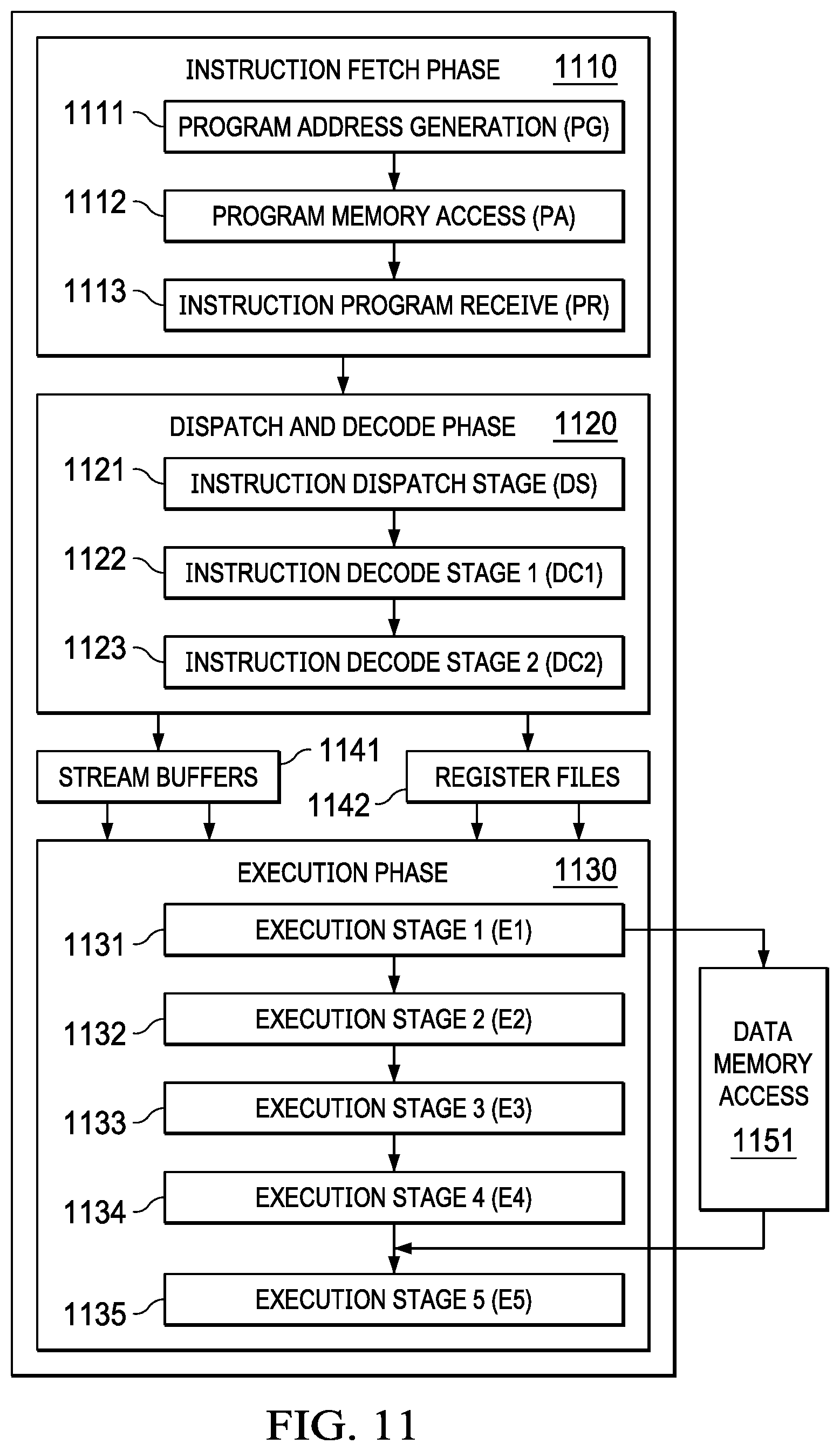
FIG. 11 illustrates the following pipeline phases: program fetch phase 1110, dispatch and decode phases 1120, and execution phases 1130. Program fetch phase 1110 includes three stages for all instructions. Dispatch and decode phases 1120 include three stages for all instructions. Execution phase 1130 includes one to four stages depending on the instruction.
Fetch phase 1110 includes program address generation (PG) stage 1111, program access (PA) stage 1112 and program receive (PR) stage 1113. During program address generation stage 1111, the program address is generated in the processor and the read request is sent to the memory controller for the L1I cache. During the program access stage 1112, the L1I cache processes the request, accesses the data in its memory and sends a fetch packet to the processor boundary. During the program receive stage 1113, the processor registers the fetch packet.
Instructions are fetched in a fetch packet that includes sixteen 32-bit wide words. FIG. 12 illustrates sixteen instructions 1201 to 1216 of a single fetch packet. Fetch packets are aligned on 512-bit (16-word) boundaries. This example employs a fixed 32-bit instruction length which enables decoder alignment. A properly aligned instruction fetch can load multiple instructions into parallel instruction decoders. Such a properly aligned instruction fetch can be achieved by predetermined instruction alignment when stored in memory by having fetch packets aligned on 512-bit boundaries coupled with a fixed instruction packet fetch. Conversely, variable length instructions require an initial step of locating each instruction boundary before decoding. A fixed length instruction set generally permits more regular layout of instruction fields which simplifies the construction of each decoder which is an advantage for a wide issue VLIW processor.
The execution of the individual instructions is partially controlled by a p bit in each instruction. In this example, the p bit is bit 0 of the 32-bit wide slot. The p bit determines whether an instruction executes in parallel with the next instruction. In this example, instructions are scanned from lower to higher address. If the p bit of an instruction is 1, then the next following instruction (higher memory address) is executed in parallel with (in the same cycle as) that instruction. If the p bit of an instruction is 0, then the next following instruction is executed in the cycle after the instruction.
Processor core 110 (FIG. 1) and L1I cache 121 pipelines (FIG. 1) are de-coupled from each other. Fetch packet returns from L1I cache can take a different number of clock cycles, depending on external circumstances such as whether there is a hit in L1I cache 121 or a hit in L2 combined cache 130. Therefore, program access stage 1112 can take several clock cycles instead of one clock cycle as in the other stages.
The instructions executing in parallel constitute an execute packet. In this example, an execute packet can contain up to sixteen 32-bit wide slots for sixteen instructions. No two instructions in an execute packet can use the same functional unit. A slot is one of five types: 1) a self-contained instruction executed on one of the functional units of processor core 110 (L1 unit 221, S1 unit 222, M1 unit 223, N1 unit 224, D1 unit 225, D2 unit 226, L2 unit 241, S2 unit 242, M2 unit 243, N2 unit 244, C unit 245 and P unit 246); 2) a unitless instruction such as a NOP (no operation) instruction or multiple NOP instruction; 3) a branch instruction; 4) a constant field extension; and 5) a conditional code extension. Some of these slot types are further explained herein.
Dispatch and decode phases 1120 (FIG. 11) include instruction dispatch to appropriate execution unit (DS) stage 1121, instruction pre-decode (DC1) stage 1122, and instruction decode, operand read (DC2) stage 1123. During instruction dispatch to appropriate execution unit stage 1121, the fetch packets are split into execute packets and assigned to the appropriate functional units. During the instruction pre-decode stage 1122, the source registers, destination registers, and associated paths are decoded for the execution of the instructions in the functional units. During the instruction decode, operand read stage 1123, more detailed unit decodes are performed and operands are read from the register files.
Execution phase 1130 includes execution (E1 to E5) stages 1131 to 1135. Different types of instructions require different numbers of such stages to complete execution. The execution stages of the pipeline play an important role in understanding the device state at processor cycle boundaries.
During E1 stage 1131, the conditions for the instructions are evaluated and operands are operated on. As illustrated in FIG. 11, E1 stage 1131 can receive operands from a stream buffer 1141 and one of the register files shown schematically as 1142. For load and store instructions, address generation is performed, and address modifications are written to a register file. For branch instructions, the branch fetch packet in PG phase 1111 is affected. As illustrated in FIG. 11, load and store instructions access memory here shown schematically as memory 1151. For single-cycle instructions, results are written to a destination register file when any conditions for the instructions are evaluated as true. If a condition is evaluated as false, the instruction does not write any results or have any pipeline operation after E1 stage 1131.
During E2 stage 1132, load instructions send the address to memory. Store instructions send the address and data to memory. Single-cycle instructions that saturate results set the SAT bit in the control status register (CSR) if saturation occurs. For 2-cycle instructions, results are written to a destination register file.
During E3 stage 1133, data memory accesses are performed. Any multiply instructions that saturate results set the SAT bit in the control status register (CSR) if saturation occurs. For 3-cycle instructions, results are written to a destination register file.
During E4 stage 1134, load instructions bring data to the processor boundary. For 4-cycle instructions, results are written to a destination register file.
During E5 stage 1135, load instructions write data into a register as illustrated schematically in FIG. 11 with input from memory 1151 to E5 stage 1135.
FIG. 13 illustrates an example of the instruction coding 1300 of functional unit instructions used by this example. Each instruction includes 32 bits and controls the operation of one of the individually controllable functional units (L1 unit 221, S1 unit 222, M1 unit 223, N1 unit 224, D1 unit 225, D2 unit 226, L2 unit 241, S2 unit 242, M2 unit 243, N2 unit 244, C unit 245 and P unit 246).
The creg field 1301 (bits 29 to 31) and the z bit 1302 (bit 28) are optional fields used in conditional instructions. The bits are used for conditional instructions to identify the predicate register and the condition. The z bit 1302 (bit 28) indicates whether the predication is based upon zero or not zero in the predicate register. If z=1, the test is for equality with zero. If z=0, the test is for nonzero. The case of creg=0 and z=0 is treated as true to allow unconditional instruction execution. The creg field 1301 and the z field 1302 are encoded in the instruction as shown in Table 1.
TABLE-US-00001 TABLE 1 Conditional creg z Register 31 30 29 28 Unconditional 0 0 0 0 Reserved 0 0 0 1 A0 0 0 1 z A1 0 1 0 z A2 0 1 1 z A3 1 0 0 z A4 1 0 1 z A5 1 1 0 z Reserved 1 1 x x
Execution of a conditional instruction is conditional upon the value stored in the specified data register. The data register is in the global scalar register file 211 for all functional units. Note that "z" in the z bit column refers to the zero/not zero comparison selection noted above and "x" is a don't care state. This coding specifies a subset of the sixteen global registers as predicate registers which preserves bits in the instruction coding. Note that unconditional instructions do not have the optional bits. For unconditional instructions, the bits in fields 1301 and 1302 (28 to 31) are used as additional opcode bits.
The dst field 1303 (bits 23 to 27) specifies a register in a corresponding register file as the destination of the instruction results.
The src2/cst field 1304 (bits 18 to 22) has several meanings depending on the instruction opcode field (bits 3 to 12 for all instructions and additionally bits 28 to 31 for unconditional instructions). One meaning specifies a register of a corresponding register file as the second operand. Another meaning is an immediate constant. Depending on the instruction type, the field 1304 is treated as an unsigned integer and zero extended to a specified data length or is treated as a signed integer and sign extended to the specified data length.
The src1 field 1305 (bits 13 to 17) specifies a register in a corresponding register file as the first source operand.
The opcode field 1306 (bits 3 to 12) for all instructions (and additionally bits 28 to 31 for unconditional instructions) specifies the type of instruction and designates appropriate instruction options including unambiguous designation of the functional unit used and operation performed. A detailed explanation of the opcode is beyond the scope of this description except for the instruction options described below.
The e bit 1307 (bit 2) is used for immediate constant instructions where the constant can be extended. If e=1, then the immediate constant is extended in a manner described below. If e=0, then the immediate constant is not extended and the immediate constant is specified by the src2/cst field 1304 (bits 18 to 22). Note that the e bit 1307 is used for some instructions. Accordingly, with proper coding, the e bit 1307 can be omitted from some instructions and the bit can be used as an additional opcode bit.
The s bit 1308 (bit 1) designates scalar data path side A 115 or vector data path side B 116. Ifs=0, then scalar data path side A 115 is selected which limits the functional unit to L1 unit 221, S1 unit 222, M1 unit 223, N1 unit 224, D1 unit 225 and D2 unit 226 and the corresponding register files illustrated in FIG. 2. Similarly, s=1 selects vector data path side B 116 which limits the functional unit to L2 unit 241, S2 unit 242, M2 unit 243, N2 unit 244, P unit 246 and the corresponding register file illustrated in FIG. 2.
The p bit 1309 (bit 0) marks the execute packets. The p-bit determines whether the instruction executes in parallel with the following instruction. The p-bits are scanned from lower to higher address. If p=1 for the current instruction, then the next instruction executes in parallel with the current instruction. If p=0 for the current instruction, then the next instruction executes in the cycle after the current instruction. All instructions executing in parallel constitute an execute packet. An execute packet can contain up to sixteen instructions. Each instruction in an execute packet uses a different functional unit.
There are two different condition code extension slots. Each execute packet can contain one each of these unique 32-bit condition code extension slots which contains the 4-bit creg/z fields for the instructions in the same execute packet. FIG. 14 illustrates the coding for condition code extension slot 0 and FIG. 15 illustrates the coding for condition code extension slot 1.
FIG. 14 illustrates the coding for condition code extension slot 0 1400 having 32 bits. Field 1401 (bits 28 to 31) specifies 4 creg/z bits assigned to the L1 unit 221 instruction in the same execute packet. Field 1402 (bits 27 to 24) specifies four creg/z bits assigned to the L2 unit 241 instruction in the same execute packet. Field 1403 (bits 20 to 23) specifies four creg/z bits assigned to the S1 unit 222 instruction in the same execute packet. Field 1404 (bits 16 to 19) specifies four creg/z bits assigned to the S2 unit 242 instruction in the same execute packet. Field 1405 (bits 12 to 15) specifies four creg/z bits assigned to the D1 unit 225 instruction in the same execute packet. Field 1406 (bits 8 to 11) specifies four creg/z bits assigned to the D2 unit 226 instruction in the same execute packet. Field 1407 (bits 6 and 7) is unused/reserved. Field 1408 (bits 0 to 5) is coded as a set of unique bits (CCEX0) to identify the condition code extension slot 0. Once the unique ID of condition code extension slot 0 is detected, the corresponding creg/z bits are employed to control conditional execution of any L1 unit 221, L2 unit 241, S1 unit 222, S2 unit 242, D1 unit 225 and D2 unit 226 instruction in the same execution packet. The creg/z bits are interpreted as shown in Table 1. If the corresponding instruction is conditional (includes creg/z bits), the corresponding bits in the condition code extension slot 0 override the condition code bits in the instruction. Setting the creg/z bits equal to "0000" makes the instruction unconditional. Thus, a properly coded condition code extension slot 0 can make some corresponding instructions conditional and some unconditional.
FIG. 15 illustrates the coding for condition code extension slot 1 1500 having 32 bits. Field 1501 (bits 28 to 31) specifies four creg/z bits assigned to the M1 unit 223 instruction in the same execute packet. Field 1502 (bits 27 to 24) specifies four creg/z bits assigned to the M2 unit 243 instruction in the same execute packet. Field 1503 (bits 19 to 23) specifies four creg/z bits assigned to the C unit 245 instruction in the same execute packet. Field 1504 (bits 16 to 19) specifies four creg/z bits assigned to the N1 unit 224 instruction in the same execute packet. Field 1505 (bits 12 to 15) specifies four creg/z bits assigned to the N2 unit 244 instruction in the same execute packet. Field 1506 (bits 6 to 11) is unused/reserved. Field 1507 (bits 0 to 5) is coded as a set of unique bits (CCEX1) to identify the condition code extension slot 1. Once the unique ID of condition code extension slot 1 is detected, the corresponding creg/z bits are employed to control conditional execution of any M1 unit 223, M2 unit 243, C unit 245, N1 unit 224 and N2 unit 244 instruction in the same execution packet. These creg/z bits are interpreted as shown in Table 1. If the corresponding instruction is conditional (includes creg/z bits), the corresponding bits in the condition code extension slot 1 override the condition code bits in the instruction. Setting the creg/z bits equal to "0000" makes the instruction unconditional. Thus, a properly coded condition code extension slot 1 can make some instructions conditional and some unconditional.
Both condition code extension slot 0 and condition code extension slot 1 can include a p bit to define an execute packet as described above in conjunction with FIG. 13. In this example, as illustrated in FIGS. 14 and 15, code extension slot 0 and condition code extension slot 1 have bit 0 (p bit) encoded as 1. Thus, neither condition code extension slot 0 nor condition code extension slot 1 can be in the last instruction slot of an execute packet.
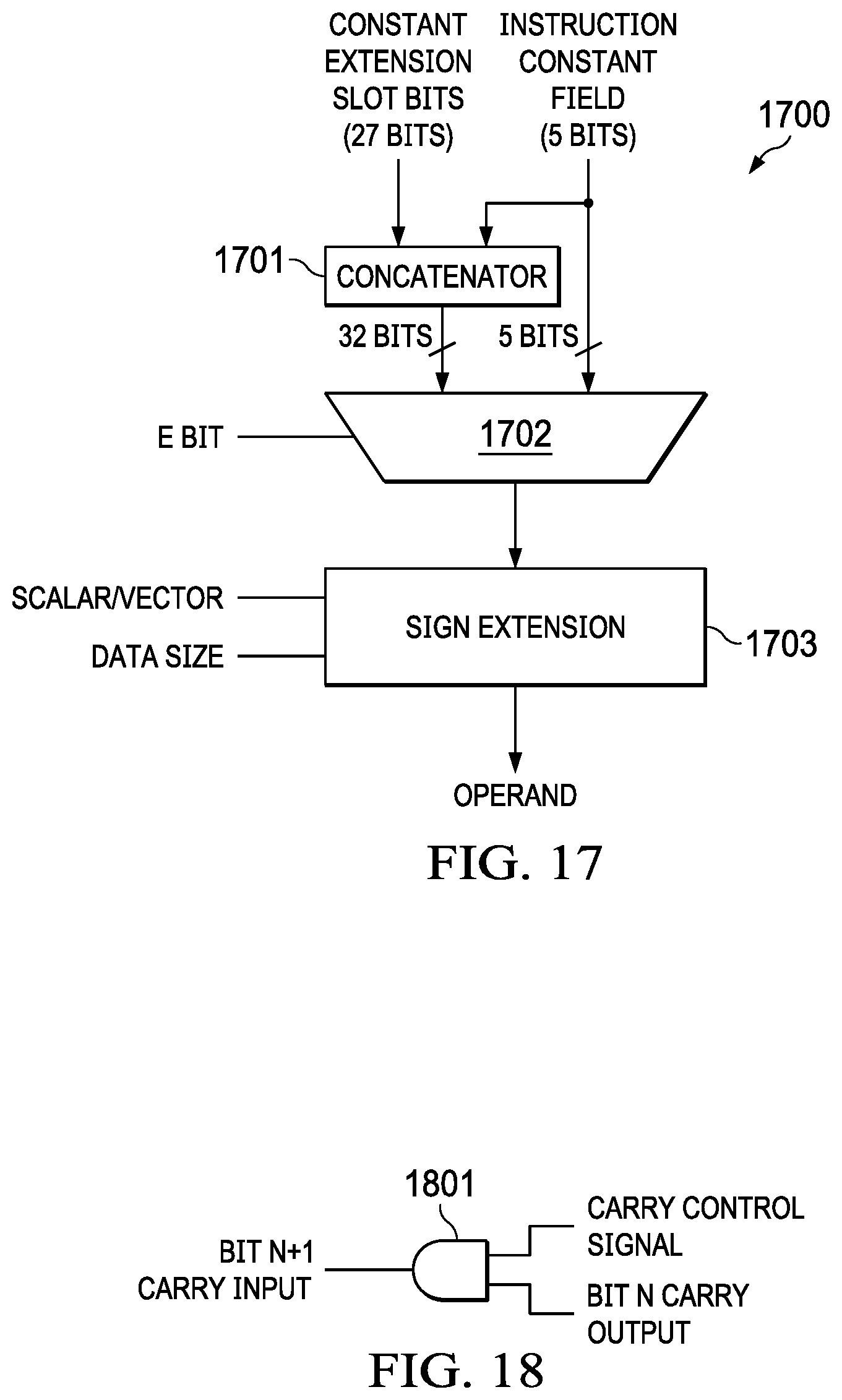
There are two different 32-bit constant extension slots. Each execute packet can contain one each of the unique constant extension slots which contains 27 bits to be concatenated as high order bits with the 5-bit constant field 1305 to form a 32-bit constant. As noted in the instruction coding description above, some instructions define the src2/cst field 1304 as a constant rather than a source register identifier. At least some of such instructions can employ a constant extension slot to extend the constant to 32 bits.
FIG. 16 illustrates the fields of constant extension slot 0 1600. Each execute packet can include one instance of constant extension slot 0 and one instance of constant extension slot 1. FIG. 16 illustrates that constant extension slot 0 1600 includes two fields. Field 1601 (bits 5 to 31) constitutes the most significant 27 bits of an extended 32-bit constant including the target instruction scr2/cst field 1304 as the five least significant bits. Field 1602 (bits 0 to 4) is coded as a set of unique bits (CSTX0) to identify the constant extension slot 0. In this example, constant extension slot 0 1600 can be used to extend the constant of one of an L1 unit 221 instruction, data in a D1 unit 225 instruction, an S2 unit 242 instruction, an offset in a D2 unit 226 instruction, an M2 unit 243 instruction, an N2 unit 244 instruction, a branch instruction, or a C unit 245 instruction in the same execute packet. Constant extension slot 1 is similar to constant extension slot 0 except that bits 0 to 4 are coded as a set of unique bits (CSTX1) to identify the constant extension slot 1. In this example, constant extension slot 1 can be used to extend the constant of one of an L2 unit 241 instruction, data in a D2 unit 226 instruction, an S1 unit 222 instruction, an offset in a D1 unit 225 instruction, an M1 unit 223 instruction or an N1 unit 224 instruction in the same execute packet.
Constant extension slot 0 and constant extension slot 1 are used as follows. The target instruction is of the type permitting constant specification. In this example, the extension is implemented by replacing one input operand register specification field with the least significant bits of the constant as described above with respect to scr2/cst field 1304. Instruction decoder 113 determines this case, known as an immediate field, from the instruction opcode bits. The target instruction also includes one constant extension bit (e bit 1307) dedicated to signaling whether the specified constant is not extended (constant extension bit=0) or extended (constant extension bit=1). If instruction decoder 113 detects a constant extension slot 0 or a constant extension slot 1, instruction decoder 113 further checks the other instructions within the execute packet for an instruction corresponding to the detected constant extension slot. A constant extension is made if one corresponding instruction has a constant extension bit (e bit 1307) equal to 1.
FIG. 17 is a partial block diagram 1700 illustrating constant extension. FIG. 17 assumes that instruction decoder 113 (FIG. 1) detects a constant extension slot and a corresponding instruction in the same execute packet. Instruction decoder 113 supplies the twenty-seven extension bits from the constant extension slot (bit field 1601) and the five constant bits (bit field 1305) from the corresponding instruction to concatenator 1701. Concatenator 1701 forms a single 32-bit word from these two parts. In this example, the twenty-seven extension bits from the constant extension slot (bit field 1601) are the most significant bits and the five constant bits (bit field 1305) are the least significant bits. The combined 32-bit word is supplied to one input of multiplexer 1702. The five constant bits from the corresponding instruction field 1305 supply a second input to multiplexer 1702. Selection of multiplexer 1702 is controlled by the status of the constant extension bit. If the constant extension bit (e bit 1307) is 1 (extended), multiplexer 1702 selects the concatenated 32-bit input. If the constant extension bit is 0 (not extended), multiplexer 1702 selects the five constant bits from the corresponding instruction field 1305. The output of multiplexer 1702 supplies an input of sign extension unit 1703.
Sign extension unit 1703 forms the final operand value from the input from multiplexer 1703. Sign extension unit 1703 receives control inputs Scalar/Vector and Data Size. The Scalar/Vector input indicates whether the corresponding instruction is a scalar instruction or a vector instruction. The functional units of data path side A 115 (L1 unit 221, S1 unit 222, M1 unit 223, N1 unit 224, D1 unit 225 and D2 unit 226) perform scalar instructions. Any instruction directed to one of these functional units is a scalar instruction. Data path side B functional units L2 unit 241, S2 unit 242, M2 unit 243, N2 unit 244 and C unit 245 can perform scalar instructions or vector instructions. Instruction decoder 113 determines whether the instruction is a scalar instruction or a vector instruction from the opcode bits. P unit 246 may performs scalar instructions. The Data Size can be eight bits (byte B), sixteen bits (half-word H), 32 bits (word W), or 64 bits (double word D).
Table 2 lists the operation of sign extension unit 1703 for the various options.
TABLE-US-00002 TABLE 2 Instruction Operand Constant Type Size Length Action Scalar B/H/W/D 5 bits Sign extend to 64 bits Scalar B/H/W/D 32 bits Sign extend to 64 bits Vector B/H/W/D 5 bits Sign extend to operand size and replicate across whole vector Vector B/H/W 32 bits Replicate 32-bit constant across each 32-bit (W) lane Vector D 32 bits Sign extend to 64 bits and replicate across each 64-bit (D) lane
Both constant extension slot 0 and constant extension slot 1 can include a p bit to define an execute packet as described above in conjunction with FIG. 13. In this example, as in the case of the condition code extension slots, constant extension slot 0 and constant extension slot 1 have bit 0 (p bit) encoded as 1. Thus, neither constant extension slot 0 nor constant extension slot 1 can be in the last instruction slot of an execute packet.
An execute packet can include a constant extension slot 0 or 1 and more than one corresponding instruction marked constant extended (e bit=1). For such an occurrence, for constant extension slot 0, more than one of an L1 unit 221 instruction, data in a D1 unit 225 instruction, an S2 unit 242 instruction, an offset in a D2 unit 226 instruction, an M2 unit 243 instruction or an N2 unit 244 instruction in an execute packet can have an e bit of 1. For such an occurrence, for constant extension slot 1, more than one of an L2 unit 241 instruction, data in a D2 unit 226 instruction, an S1 unit 222 instruction, an offset in a D1 unit 225 instruction, an M1 unit 223 instruction or an N1 unit 224 instruction in an execute packet can have an e bit of 1. In one example, instruction decoder 113 determines that such an occurrence is an invalid operation and not supported. Alternately, the combination can be supported with extension bits of the constant extension slot applied to each corresponding functional unit instruction marked constant extended.
L1 unit 221, S1 unit 222, L2 unit 241, S2 unit 242 and C unit 245 often operate in a single instruction multiple data (SIMD) mode. In this SIMD mode, the same instruction is applied to packed data from the two operands. Each operand holds multiple data elements disposed in predetermined slots. SIMD operation is enabled by carry control at the data boundaries. Such carry control enables operations on varying data widths.
FIG. 18 illustrates the carry control logic. AND gate 1801 receives the carry output of bit N within the operand wide arithmetic logic unit (64 bits for scalar data path side A 115 functional units and 512 bits for vector data path side B 116 functional units). AND gate 1801 also receives a carry control signal which is further explained below. The output of AND gate 1801 is supplied to the carry input of bit N+1 of the operand wide arithmetic logic unit. AND gates such as AND gate 1801 are disposed between every pair of bits at a possible data boundary. For example, for 8-bit data such an AND gate will be between bits 7 and 8, bits 15 and 16, bits 23 and 24, etc. Each such AND gate receives a corresponding carry control signal. If the data size is the minimum size, each carry control signal is 0, effectively blocking carry transmission between the adjacent bits. The corresponding carry control signal is 1 if the selected data size requires both arithmetic logic unit sections. Table 3 below shows example carry control signals for the case of a 512-bit wide operand as used by vector data path side B 116 functional units which can be divided into sections of 8 bits, 16 bits, 32 bits, 64 bits, 128 bits or 256 bits. In Table 3, the upper 32 bits control the upper bits (bits 128 to 511) carries and the lower 32 bits control the lower bits (bits 0 to 127) carries. No control of the carry output of the most significant bit is needed, thus only 63 carry control signals are required.
TABLE-US-00003 TABLE 3 Data Size Carry Control Signals 8 bits (B) -000 0000 0000 0000 0000 0000 0000 0000 0000 0000 0000 0000 0000 0000 0000 0000 16 bits (H) -101 0101 0101 0101 0101 0101 0101 0101 0101 0101 0101 0101 0101 0101 0101 0101 32 bits (W) -111 0111 0111 0111 0111 0111 0111 0111 0111 0111 0111 0111 0111 0111 0111 0111 64 bits (D) -111 1111 0111 1111 0111 1111 0111 1111 0111 1111 0111 1111 0111 1111 0111 1111 128 bits -111 1111 1111 1111 0111 1111 1111 1111 0111 1111 1111 1111 0111 1111 1111 1111 256 bits -111 1111 1111 1111 1111 1111 1111 1111 0111 1111 1111 1111 1111 1111 1111 1111
Operation on data sizes that are integral powers of 2 (2.sup.N) is common. However, the carry control technique is not limited to integral powers of 2 and can be applied to other data sizes and operand widths.
In this example, at least L unit 241 and S unit 242 employ two types of SIMD instructions using registers in predicate register file 234. In this example, the SIMD vector predicate instructions operate on an instruction specified data size. The data sizes include byte (8 bit) data, half word (16 bit) data, word (32 bit) data, double word (64 bit) data, quad word (128 bit) data and half vector (256 bit) data. In the first of these instruction types, the functional unit (L unit 241 or S unit 242) performs a SIMD comparison on packed data in two general data registers and supplies results to a predicate data register. The instruction specifies a data size, the two general data register operands, and the destination predicate register. In this example, each predicate data register includes one bit corresponding to each minimal data size portion of the general data registers. In the current example, the general data registers are 512 bits (64 bytes) and the predicate data registers are 64 bits (8 bytes). Each bit of a predicate data register corresponds to eight bits of a general data register. The comparison is performed on a specified data size (8, 16, 32, 64, 128 or 256 bits). If the comparison is true, then the functional unit supplies 1's to all predicate register bits corresponding the that data size portion. If the comparison is false, the functional unit supplies zeroes to the predicate register bits corresponding to that data size portion. In this example, the enabled comparison operations include: less than, greater than, and equal to.
In the second of the instruction types, the functional unit (L unit 241 or S unit 242) separately performs a first SIMD operation or a second SIMD operation on packed data in general data registers based upon the state of data in a predicate data register. The instruction specifies a data size, one or two general data register operands, a controlling predicate register, and a general data register destination. For example, a functional unit can select, for each data sized portion of two vector operands, a first data element of a first operand or a second data element of a second operand dependent upon the I/O state of corresponding bits in the predicate data register to store in the destination register. In another example, the data elements of a single vector operand can be saved to memory or not saved dependent upon the data of the corresponding bits of the predicate register.
The operations of P unit 245 permit a variety of compound vector SIMD operations based upon more than one vector comparison. For example, a range determination can be made using two comparisons. In a SIMD operation, a candidate vector is compared with a vector reference having the minimum of the range packed within a data register. The greater than result is scalar data with bits corresponding to the SIMD data width set to 0 or 1 depending upon the SIMD comparison and is stored in a predicate data register. Another SIMD comparison of the candidate vector is performed with another reference vector having the maximum of the range packed within a different data register produces another scalar with less than results stored in another predicate register. The P unit then ANDs the two predicate registers. The AND result indicates whether each SIMD data part of the candidate vector is within range or out of range. A P unit BITCNT instruction of the AND result can produce a count of the data elements within the comparison range. The P unit NEG function can be used to convert: a less than comparison result to a greater than or equal comparison result; a greater than comparison result to a less than or equal to comparison result; or, an equal to comparison result to a not equal to comparison result.
Streaming Engine
FIG. 19 is a conceptual view of the streaming engine 125 of the example processor 100 of FIG. 1. FIG. 19 illustrates the processing of a single stream representative of the two streams controlled by streaming engine 125. Streaming engine 1900 includes stream address generator 1901. Stream address generator 1901 sequentially generates addresses of the elements of the stream and supplies these element addresses to system memory 1910. Memory 1910 recalls data stored at the element addresses (data elements) and supplies these data elements to data first-in-first-out (FIFO) buffer 1902. Data FIFO buffer 1902 provides buffering between memory 1910 and processor 1920. Data formatter 1903 receives the data elements from data FIFO memory 1902 and provides data formatting according to the stream definition. This process is described in more detail herein. Streaming engine 1900 supplies the formatted data elements from data formatter 1903 to the processor 1920. A program executing on processor 1920 consumes the data and generates an output.
Stream elements typically reside in system memory. The memory imposes no particular structure upon the stream. Programs define streams and thereby impose structure by specifying the stream attributes such as address of the first element of the stream, size and type of the elements in the stream, formatting for data in the stream, and the address sequence associated with the stream.
The streaming engine defines an address sequence for elements of the stream in terms of a pointer walking through memory. A multiple-level nested loop controls the path the pointer takes. An iteration count for a loop level indicates the number of times the level repeats. A dimension gives the distance between pointer positions of the loop level.
In a basic forward stream, the innermost loop consumes physically contiguous elements from memory as the implicit dimension of the innermost loop is one element. The pointer moves from element to element in consecutive, increasing order. In each level outside the inner loop, that loop moves the pointer to a new location based on the size of the dimension of the loop level.
This form of addressing allows programs to specify regular paths through memory using a small number of parameters. Table 4 lists the addressing parameters of a basic stream.
TABLE-US-00004 TABLE 4 Parameter Definition ELEM_BYTES Size of each element in bytes ICNT0 Number of iterations for the innermost loop level 0. At loop level 0 all elements are physically contiguous. Implied DIM0 = ELEM_BYTES ICNT1 Number of iterations for loop level 1 DIM1 Number of bytes between the starting points for consecutive iterations of loop level 1 ICNT2 Number of iterations for loop level 2 DIM2 Number of bytes between the starting points for consecutive iterations of loop level 2 ICNT3 Number of iterations for loop level 3 DIM3 Number of bytes between the starting points for consecutive iterations of loop level 3 ICNT4 Number of iterations for loop level 4 DIM4 Number of bytes between the starting points for consecutive iterations of loop level 4 ICNT5 Number of iterations for loop level 5 DIMS Number of bytes between the starting points for consecutive iterations of loop level 5
In this example, ELEM_BYTES ranges from 1 to 64 bytes as shown in Table 5.
TABLE-US-00005 TABLE 5 ELEM_BYTES Stream Element Length 000 1 byte 001 2 bytes 010 4 bytes 011 8 bytes 100 16 bytes 101 32 bytes 110 64 bytes 111 Reserved
The definition above maps consecutive elements of the stream to increasing addresses in memory which is appropriate for many algorithms. Some algorithms are better served by reading elements in decreasing memory address order or reverse stream addressing. For example, a discrete convolution computes vector dot-products, as illustrated by expression (1). (f*g)[t]=.SIGMA..sub.x.sup.=-.infin.f[x]g[t-x] (1)
In expression (1), f[ ] and g[ ] represent arrays in memory. For each output, the algorithm reads f[ ] in the forward direction and reads g[ ] in the reverse direction. Practical filters limit the range of indices for [x] and [t-x] to a finite number of elements. To support this pattern, the streaming engine supports reading elements in decreasing address order.
Matrix multiplication presents a unique problem to the streaming engine. Each element in the matrix product is a vector dot product between a row from the first matrix and a column from the second. Programs typically store matrices in row-major or column-major order. Row-major order stores all the elements of a single row contiguously in memory. Column-major order stores all elements of a single column contiguously in memory. Matrices are typically stored in the same order as the default array order for the language. As a result, only one of the two matrices in a matrix multiplication map on to the 2-dimensional stream definition of the streaming engine. In a typical example, an index steps through columns on one array and rows of the other array. The streaming engine supports implicit matrix transposition with transposed streams. Transposed streams avoid the cost of explicitly transforming the data in memory. Instead of accessing data in strictly consecutive-element order, the streaming engine effectively interchanges the inner two loop dimensions of the traversal order, fetching elements along the second dimension into contiguous vector lanes.
This algorithm works but is impractical to implement for small element sizes. Some algorithms work on matrix tiles which are multiple columns and rows together. Therefore, the streaming engine defines a separate transposition granularity. The hardware imposes a minimum granularity. The transpose granularity needs to be at least as large as the element size. Transposition granularity causes the streaming engine to fetch one or more consecutive elements from dimension 0 before moving along dimension 1. When the granularity equals the element size, a single column from a row-major array is fetched. Otherwise, the granularity specifies fetching two, four or more columns at a time from a row-major array. This is also applicable for column-major layout by exchanging row and column in the description. A parameter GRANULE indicates the transposition granularity in bytes.
Another common matrix multiplication technique exchanges the innermost two loops of the matrix multiply. The resulting inner loop no longer reads down the column of one matrix while reading across the row of another. For example, the algorithm may hoist one term outside the inner loop, replacing it with the scalar value. The innermost loop can be implemented with a single scalar by vector multiply followed by a vector add. Or, the scalar value can be duplicated across the length of the vector and a vector by vector multiply used. The streaming engine of this example directly supports the latter case and related use models with an element duplication mode. In this mode, the streaming engine reads a granule smaller than the full vector size and replicates that granule to fill the next vector output.
The streaming engine treats each complex number as a single element with two sub-elements that give the real and imaginary (rectangular) or magnitude and angle (polar) portions of the complex number. Not all programs or peripherals agree what order these sub-elements should appear in memory. Therefore, the streaming engine offers the ability to swap the two sub-elements of a complex number with no cost. The feature swaps the halves of an element without interpreting the contents of the element and can be used to swap pairs of sub-elements of any type, not just complex numbers.
Algorithms generally prefer to work at high precision, but high precision values require more storage and bandwidth than lower precision values. Commonly, programs store data in memory at low precision, promote those values to a higher precision for calculation, and then demote the values to lower precision for storage. The streaming engine supports such operations directly by allowing algorithms to specify one level of type promotion. In this example, every sub-element can be promoted to a larger type size with either sign or zero extension for integer types. In some examples, the streaming engine supports floating point promotion, promoting 16-bit and 32-bit floating point values to 32-bit and 64-bit formats, respectively.
While the streaming engine defines a stream as a discrete sequence of data elements, the processing unit core 110 consumes data elements packed contiguously in vectors. The vectors resemble streams as the vectors contain multiple homogeneous elements with some implicit sequence. Because the streaming engine reads streams, but the processing unit core 110 consumes vectors, the streaming engine maps streams onto vectors in a consistent way.
Vectors include equal-sized lanes, each lane containing a sub-element. The processing unit core 110 designates the rightmost lane of the vector as lane 0, regardless of current endian mode. Lane numbers increase right-to-left. The actual number of lanes within a vector varies depending on the length of the vector and the data size of the sub-element.
FIG. 20 illustrates the sequence of the formatting operations of formatter 1903. Formatter 1903 includes three sections: input section 2010, formatting section 2020, and output section 2030. Input section 2010 receives the data recalled from system memory 1910 as accessed by stream address generator 1901. The data can be via linear fetch stream 2011 or transposed fetch stream 2012.
Formatting section 2020 includes various formatting blocks. The formatting performed within formatter 1903 by the blocks is further described below. Complex swap block 2021 optionally swaps two sub-elements forming a complex number element. Type promotion block 2022 optionally promotes each data element into a larger data size. Promotion includes zero extension for unsigned integers and sign extension for signed integers. Decimation block 2023 optionally decimates the data elements. In this example, decimation can be 2:1 retaining every other data element or 4:1 retaining every fourth data element. Element duplication block 2024 optionally duplicates individual data elements. In this example, the data element duplication is an integer power of 2 (2N, where N is an integer) including 2.times., 4.times., 8.times., 16.times., 32.times. and 64.times.. In this example, data duplication can extend over multiple destination vectors. Vector length masking/group duplication block 2025 has two primary functions. An independently specified vector length VECLEN controls the data elements supplied to each output data vector. When group duplication is off, excess lanes in the output data vector are zero filled and these lanes are marked invalid. When group duplication is on, input data elements of the specified vector length are duplicated to fill the output data vector.
Output section 2030 holds the data for output to the corresponding functional units. Register and buffer for processor 2031 stores a formatted vector of data to be used as an operand by the functional units of processing unit core 110 (FIG. 1).
FIG. 21 illustrates an example of lane allocation in a vector. Vector 2100 is divided into eight 64-bit lanes (8.times.64 bits=512 bits, the vector length). Lane 0 includes bits 0 to 63, lane 1 includes bits 64 to 127, lane 2 includes bits 128 to 191, lane 3 includes bits 192 to 255, lane 4 includes bits 256 to 319, lane 5 includes bits 320 to 383, lane 6 includes bits 384 to 447, and lane 7 includes bits 448 to 511.
FIG. 22 illustrates another example of lane allocation in a vector. Vector 2210 is divided into sixteen 32-bit lanes (16.times.32 bits=512 bits, the vector length). Lane 0 includes bits 0 to 31, lane 1 includes bits 32 to 63, lane 2 includes bits 64 to 95, lane 3 includes bits 96 to 127, lane 4 includes bits 128 to 159, lane 5 includes bits 160 to 191, lane 6 includes bits 192 to 223, lane 7 includes bits 224 to 255, lane 8 includes bits 256 to 287, lane 9 includes bits 288 to 319, lane 10 includes bits 320 to 351, lane 11 includes bits 352 to 383, lane 12 includes bits 384 to 415, lane 13 includes bits 416 to 447, lane 14 includes bits 448 to 479, and lane 15 includes bits 480 to 511.
The streaming engine maps the innermost stream dimension directly to vector lanes. The streaming engine maps earlier elements within the innermost stream dimension to lower lane numbers and later elements to higher lane numbers, regardless of whether the stream advances in increasing or decreasing address order. Whatever order the stream defines, the streaming engine deposits elements in vectors in increasing-lane order. For non-complex data, the streaming engine places the first element in lane 0 of the vector processing unit core 110 (FIG. 1) fetches, the second in lane 1, and so on. For complex data, the streaming engine places the first element in lanes 0 and 1, the second element in lanes 2 and 3, and so on. Sub-elements within an element retain the same relative ordering regardless of the stream direction. For non-swapped complex elements, the sub-elements with the lower address of each pair are placed in the even numbered lanes, and the sub-elements with the higher address of each pair are placed in the odd numbered lanes. For swapped complex elements, the placement is reversed.
The streaming engine fills each vector processing unit core 110 fetches with as many elements as possible from the innermost stream dimension. If the innermost dimension is not a multiple of the vector length, the streaming engine zero pads the dimension to a multiple of the vector length. As noted below, the streaming engine also marks the lanes invalid. Thus, for higher-dimension streams, the first element from each iteration of an outer dimension arrives in lane 0 of a vector. The streaming engine maps the innermost dimension to consecutive lanes in a vector. For transposed streams, the innermost dimension includes groups of sub-elements along dimension 1, not dimension 0, as transposition exchanges these two dimensions.
Two-dimensional (2D) streams exhibit greater variety as compared to one-dimensional streams. A basic 2D stream extracts a smaller rectangle from a larger rectangle. A transposed 2D stream reads a rectangle column-wise instead of row-wise. A looping stream, where the second dimension overlaps first, executes a finite impulse response (FIR) filter taps which loops repeatedly over FIR filter samples providing a sliding window of input samples.
FIG. 23 illustrates a region of memory that can be accessed using a basic two-dimensional stream. The inner two dimensions, represented by ELEM_BYTES, ICNT0, DIM1 and ICNT1 (refer to Table 4), give sufficient flexibility to describe extracting a smaller rectangle 2320 having dimensions 2321 and 2322 from a larger rectangle 2310 having dimensions 2311 and 2312. In this example, rectangle 2320 is a 9 by 13 rectangle of 64-bit values and rectangle 2310 is a larger 11 by 19 rectangle. The following stream parameters define this stream: ICNT0=9, ELEM_BYTES=8, ICNT1=13, and DIM1=88 (11 times 8).
Thus, the iteration count in the 0-dimension 2321 is nine and the iteration count in the 1-dimension 2322 is thirteen. Note that the ELEM_BYTES scales the innermost dimension. The first dimension has ICNT0 elements of size ELEM_BYTES. The stream address generator does not scale the outer dimensions. Therefore, DIM1=88, which is eleven elements scaled by eight bytes per element.
FIG. 24 illustrates the order of elements within the example stream of FIG. 23. The streaming engine fetches elements for the stream in the order illustrated in order 2400. The first nine elements come from the first row of rectangle 2320, left-to-right in hops 1 to 8. The 10th through 24th elements comes from the second row, and so on. When the stream moves from the 9th element to the 10th element (hop 9 in FIG. 24), the streaming engine computes the new location based on the position of the pointer at the start of the inner loop, not the position of the pointer at the end of the first dimension. Thus, DIM1 is independent of ELEM_BYTES and ICNT0. DIM1 represents the distance between the first bytes of each consecutive row.
Transposed streams are accessed along dimension 1 before dimension 0. The following examples illustrate transposed streams with varying transposition granularity. FIG. 25 illustrates extracting a smaller rectangle 2520 (12.times.8) having dimensions 2521 and 2522 from a larger rectangle 2510 (14.times.13) having dimensions 2511 and 2512. In FIG. 25, ELEM_BYTES equal 2.
FIG. 26 illustrates how the streaming engine fetches the stream of the example stream of FIG. 25 with a transposition granularity of four bytes. Fetch pattern 2600 fetches pairs of elements from each row (because the granularity of four is twice the ELEM_BYTES of two), but otherwise moves down the columns. Once the streaming engine reaches the bottom of a pair of columns, the streaming engine repeats the pattern with the next pair of columns.
FIG. 27 illustrates how the streaming engine fetches the stream of the example stream of FIG. 25 with a transposition granularity of eight bytes. The overall structure remains the same. The streaming engine fetches four elements from each row (because the granularity of eight is four times the ELEM_BYTES of two) before moving to the next row in the column as shown in fetch pattern 2700.
The streams examined so far read each element from memory exactly once. A stream can read a given element from memory multiple times, in effect looping over a portion of memory. FIR filters exhibit two common looping patterns: re-reading the same filter taps for each output and reading input samples from a sliding window. Two consecutive outputs need inputs from two overlapping windows.
FIG. 28 illustrates the details of streaming engine 125 of FIG. 1. Streaming engine 125 contains three major sections: Stream 0 2810; Stream 1 2820; and Shared L2 Interfaces 2830. Stream 0 2810 and Stream 1 2820 both contain identical hardware that operates in parallel. Stream 0 2810 and Stream 1 2820 both share L2 interfaces 2830. Each stream 2810 and 2820 provides processing unit core 110 (FIG. 1) data at a rate of up to 512 bits/cycle, every cycle, which is enabled by the dedicated stream paths and shared dual L2 interfaces.
Each streaming engine 125 includes a respective dedicated 6-dimensional (6D) stream address generator 2811/2821 that can each generate one new non-aligned request per cycle. As is further described herein, address generators 2811/2821 output 512-bit aligned addresses that overlap the elements in the sequence defined by the stream parameters.
Each address generator 2811/2821 connects to a respective dedicated micro table look-aside buffer (.mu.TLB) 2812/2822. The .mu.TLB 2812/2822 converts a single 48-bit virtual address to a 44-bit physical address each cycle. Each .mu.TLB 2812/2822 has 8 entries, covering a minimum of 32 kB with 4 kB pages or a maximum of 16 MB with 2 MB pages. Each address generator 2811/2821 generates 2 addresses per cycle. The .mu.TLB 2812/2822 only translates one address per cycle. To maintain throughput, streaming engine 125 operates under the assumption that most stream references are within the same 4 kB page. Thus, the address translation does not modify bits 0 to 11 of the address. If aout0 and aou1 line in the same 4 kB page (aout0[47:12] are the same aout1[47:12]), then the .mu.TLB 2812/2822 only translates aout0 and reuses the translation for the upper bits of both addresses.
Translated addresses are queued in respective command queue 2813/2823. These addresses are aligned with information from the respective corresponding Storage Allocation and Tracking block 2814/2824. Streaming engine 125 does not explicitly manage .mu.TLB 2812/2822. The system memory management unit (MMU) invalidates .mu.TLBs as necessary during context switches.
Storage Allocation and Tracking 2814/2824 manages the internal storage of the stream, discovering data reuse and tracking the lifetime of each piece of data. The block accepts two virtual addresses per cycle and binds those addresses to slots in the internal storage. The data store is organized as an array of slots. The streaming engine maintains following metadata to track the contents and lifetime of the data in each slot: 49-bit virtual address associated with the slot, valid bit indicating valid address, ready bit indicating data has arrived for the address, active bit indicating if there are any references outstanding to this data, and a last reference value indicating the most recent reference to this slot in the reference queue. The storage allocation and tracking are further described herein.
Respective reference queue 2815/2825 stores the sequence of references generated by the respective corresponding address generator 2811/2821. The reference sequence enables the data formatting network to present data to processing unit core 110 in the correct order. Each entry in respective reference queue 2815/2825 contains the information necessary to read data out of the data store and align the data for processing unit core 110. Respective reference queue 2815/2825 maintains the information listed in Table 6 in each slot.
TABLE-US-00006 TABLE 6 Data Slot Low Slot number for the lower half of data associated with aout0 Data Slot High Slot number for the upper half of data associated with aout1 Rotation Number of bytes to rotate data to align next element with lane 0 Length Number of valid bytes in this reference
Storage allocation and tracking 2814/2824 inserts references in reference queue 2815/2825 as address generator 2811/2821 generates new addresses. Storage allocation and tracking 2814/2824 removes references from reference queue 2815/2825 when the data becomes available and there is room in the stream head registers. As storage allocation and tracking 2814/2824 removes slot references from reference queue 2815/2825 and formats data, the references are checked for the last reference to the corresponding slots. Storage allocation and tracking 2814/2824 compares reference queue 2815/2825 removal pointer against the recorded last reference of the slot. If the pointer and the recorded last reference match, then storage allocation and tracking 2814/2824 marks the slot inactive once the data is no longer needed.
Streaming engine 125 has respective data storage 2816/2826 for a selected number of elements. Deep buffering allows the streaming engine to fetch far ahead in the stream, hiding memory system latency. Each data storage 2816/2826 accommodates two simultaneous read operations and two simultaneous write operations per cycle and each is therefore referred to a two-read, two-write (2r2w) data storage. In other examples, the amount of buffering can be different. In the current example, streaming engine 125 dedicates 32 slots to each stream with each slot tagged by a virtual address. Each slot holds 64 bytes of data in eight banks of eight bytes.
Data storage 2816/2826 and the respective storage allocation/tracking logic 2814/2824 and reference queues 2815/2825 implement the data FIFO 1902 discussed with reference to FIG. 19.
Respective butterfly network 2817/2827 includes a seven-stage butterfly network. Butterfly network 2817/2827 receives 128 bytes of input and generates 64 bytes of output. The first stage of the butterfly is actually a half-stage that collects bytes from both slots that match a non-aligned fetch and merges the collected bytes into a single, rotated 64-byte array. The remaining six stages form a standard butterfly network. Respective butterfly network 2817/2827 performs the following operations: rotates the next element down to byte lane 0; promotes data types by a power of two, if requested; swaps real and imaginary components of complex numbers, if requested; and converts big endian to little endian if processing unit core 110 is presently in big endian mode. The user specifies element size, type promotion, and real/imaginary swap as part of the parameters of the stream.
Streaming engine 125 attempts to fetch and format data ahead of processing unit core 110's demand in order to maintain full throughput. Respective stream head registers 2818/2828 provide a small amount of buffering so that the process remains fully pipelined. Respective stream head registers 2818/2828 are not directly architecturally visible. Each stream also has a respective stream valid register 2819/2829. Valid registers 2819/2829 indicate which elements in the corresponding stream head registers 2818/2828 are valid.
The two streams 2810/2820 share a pair of independent L2 interfaces 2830: L2 Interface A (IFA) 2833 and L2 Interface B (IFB) 2834. Each L2 interface provides 512 bits/cycle throughput direct to the L2 controller 130 (FIG. 1) via respective buses 147/149 for an aggregate bandwidth of 1024 bits/cycle. The L2 interfaces use the credit-based multicore bus architecture (MBA) protocol. The MBA protocol is described in more detail in U.S. Pat. No. 9,904,645, "Multicore Bus Architecture with Non-Blocking High Performance Transaction Credit System," which is incorporated by reference herein. The L2 controller assigns a pool of command credits to each interface. The pool has sufficient credits so that each interface can send sufficient requests to achieve full read-return bandwidth when reading L2 RAM, L2 cache and multicore shared memory controller (MSMC) memory, as described in more detail herein.
To maximize performance, in this example both streams can use both L2 interfaces, allowing a single stream to send a peak command rate of two requests per cycle. Each interface prefers one stream over the other, but this preference changes dynamically from request to request. IFA 2833 and IFB 2834 prefer opposite streams, when IFA 2833 prefers Stream 0, IFB 2834 prefers Stream 1 and vice versa.
Respective arbiter 2831/2832 ahead of each respective interface 2833/2834 applies the following basic protocol on every cycle having credits available. Arbiter 2831/2832 checks if the preferred stream has a command ready to send. If so, arbiter 2831/2832 chooses that command. Arbiter 2831/2832 next checks if an alternate stream has at least two requests ready to send, or one command and no credits. If so, arbiter 2831/2832 pulls a command from the alternate stream. If either interface issues a command, the notion of preferred and alternate streams swap for the next request. Using this algorithm, the two interfaces dispatch requests as quickly as possible while retaining fairness between the two streams. The first rule ensures that each stream can send a request on every cycle that has available credits. The second rule provides a mechanism for one stream to borrow the interface of the other when the second interface is idle. The third rule spreads the bandwidth demand for each stream across both interfaces, ensuring neither interface becomes a bottleneck.
Respective coarse grain rotator 2835/2836 enables streaming engine 125 to support a transposed matrix addressing mode. In this mode, streaming engine 125 interchanges the two innermost dimensions of the multidimensional loop to access an array column-wise rather than row-wise. Respective rotators 2835/2836 are not architecturally visible.
FIG. 29 illustrates an example stream template register 2900. The stream definition template provides the full structure of a stream that contains data. The iteration counts and dimensions provide most of the structure, while the various flags provide the rest of the details. In this example, a single stream template 2900 is defined for all data-containing streams. All stream types supported by the streaming engine are covered by the template 2900. The streaming engine supports a six-level loop nest for addressing elements within the stream. Most of the fields in the stream template 2900 map directly to the parameters in that algorithm. The numbers above the fields are bit numbers within a 256-bit vector. Table 7 shows the stream field definitions of a stream template, which includes ICNT0 field (2901), ICNT1 field (2902), ICNT2 field (2903), ICNT3 field (2904), ICNT4 field (2905), ICNT5 field (2906), DIM1 field (2911), DIM2 field (2912), DIM3 field (2913), DIM4 field (2914), DIM5 field (2915), and FLAGS field (2921).
TABLE-US-00007 TABLE 7 FIG. 29 Field Reference Size Name Number Description Bits ICNT0 2901 Iteration count for loop 0 32 ICNT1 2902 Iteration count for loop 1 32 ICNT2 2903 Iteration count for loop 2 32 ICNT3 2904 Iteration count for loop 3 32 ICNT4 2905 Iteration count for loop 4 32 ICNT5 2906 Iteration count for loop 5 32 DIM1 2911 Signed dimension for loop 1 32 DIM2 2912 Signed dimension for loop 2 32 DIM3 2913 Signed dimension for loop 3 32 DIM4 2914 Signed dimension for loop 4 32 DIM5 2915 Signed dimension for loop 5 32 FLAGS 2921 Stream modifier flags 64
Loop 0 is the innermost loop and loop 5 is the outermost loop. In the current example, DIM0 is equal to ELEM_BYTES defining physically contiguous data. Thus, the stream template register 2900 does not define DIM0. Streaming engine 125 interprets iteration counts as unsigned integers and dimensions as unscaled signed integers. An iteration count of zero at any level (ICNT0, ICNT1, ICNT2, ICNT3, ICNT4 or ICNT5) indicates an empty stream. Each iteration count must be at least one to define a valid stream. The template above specifies the type of elements, length and dimensions of the stream. The stream instructions separately specify a start address, e.g., by specification of a scalar register in scalar register file 211 which stores the start address. Thus, a program can open multiple streams using the same template but different registers storing the start address.
FIG. 30 illustrates an example of sub-field definitions of the flags field 2911 shown in FIG. 29. As shown in FIG. 30, the flags field 2911 is 6 bytes or 48 bits. FIG. 30 shows bit numbers of the fields. Table 8 shows the definition of these fields, which include ELTYPE field (3001), TRANSPOSE field (3002), PROMOTE field (3003), VECLEN field (3004), ELDUP field (3005), GRDUP field (3006), DECIM field (3007), THROTTLE field (3008), DIMFMT field (3009), DIR field (3010), CBK0 field (3011), CBK1 field (3012), AM0 field (3013), AM1 field (3014), AM2 field (3015), AM3 field (3016), AM4 field (3017), and AM5 field (3018).
TABLE-US-00008 TABLE 8 FIG. 30 Reference Size Field Name Number Description Bits ELTYPE 3001 Type of data element 4 TRANSPOSE 3002 Two-dimensional transpose mode 3 PROMOTE 3003 Promotion mode 3 VECLEN 3004 Stream vector length 3 ELDUP 3005 Element duplication 3 GRDUP 3006 Group duplication 1 DECIM 3007 Element decimation 2 THROTTLE 3008 Fetch ahead throttle mode 2 DIMFMT 3009 Stream dimensions format 3 DIR 3010 Stream direction 1 0 forward direction 1 reverse direction CBK0 3011 First circular block size number 4 CBK1 3012 Second circular block size number 4 AM0 3013 Addressing mode for loop 0 2 AM1 3014 Addressing mode for loop 1 2 AM2 3015 Addressing mode for loop 2 2 AM3 3016 Addressing mode for loop 3 2 AM4 3017 Addressing mode for loop 4 2 AMS 3018 Addressing mode for loop 5 2
The Element Type (ELTYPE) field 3001 defines the data type of the elements in the stream. The coding of the four bits of the ELTYPE field 3001 is defined as shown in Table 9.
TABLE-US-00009 TABLE 9 Real/ Sub-element Total Element ELTYPE Complex Size Bits Size Bits 0000 real 8 8 0001 real 16 16 0010 real 32 32 0011 real 64 64 0100 reserved 0101 reserved 0110 reserved 0111 reserved 1000 complex 8 16 no swap 1001 complex 16 32 no swap 1010 complex 32 64 no swap 1011 complex 64 128 no swap 1100 complex 8 16 swapped 1101 complex 16 32 swapped 1110 complex 32 64 swapped 1111 complex 64 128 swapped
Real/Complex Type determines whether the streaming engine treats each element as a real number or two parts (real/imaginary or magnitude/angle) of a complex number and also specifies whether to swap the two parts of complex numbers. Complex types have a total element size twice the sub-element size. Otherwise, the sub-element size equals the total element size.
Sub-Element Size determines the type for purposes of type promotion and vector lane width. For example, 16-bit sub-elements get promoted to 32-bit sub-elements or 64-bit sub-elements when a stream requests type promotion. The vector lane width matters when processing unit core 110 (FIG. 1) operates in big endian mode, as the core 110 lays out vectors in little endian order.
Total Element Size specifies the minimal granularity of the stream which determines the number of bytes the stream fetches for each iteration of the innermost loop. Streams read whole elements, either in increasing or decreasing order. Therefore, the innermost dimension of a stream spans ICNT0.times.total-element-size bytes.
The TRANSPOSE field 3002 determines whether the streaming engine accesses the stream in a transposed order. The transposed order exchanges the inner two addressing levels. The TRANSPOSE field 3002 also indicated the granularity for transposing the stream. The coding of the three bits of the TRANSPOSE field 3002 is defined as shown in Table 10 for normal 2D operations.
TABLE-US-00010 TABLE 10 Transpose Meaning 000 Transpose disabled 001 Transpose on 8-bit boundaries 010 Transpose on 16-bit boundaries 011 Transpose on 32-bit boundaries 100 Transpose on 64-bit boundaries 101 Transpose on 128-bit boundaries 110 Transpose on 256-bit boundaries 111 Reserved
Streaming engine 125 can transpose data elements at a different granularity than the element size thus allowing programs to fetch multiple columns of elements from each row. The transpose granularity cannot be smaller than the element size. The TRANSPOSE field 3002 interacts with the DIMFMT field 3009 in a manner further described below.
The PROMOTE field 3003 controls whether the streaming engine promotes sub-elements in the stream and the type of promotion. When enabled, streaming engine 125 promotes types by powers-of-2 sizes. The coding of the three bits of the PROMOTE field 3003 is defined as shown in Table 11.
TABLE-US-00011 TABLE 11 Promotion Promotion Resulting Sub-element Size PROMOTE Factor Type 8-bit 16-bit 32-bit 64-bit 000 lx N/A 8-bit 16-bit 32-bit 64-bit 001 2x zero extend 16-bit 32-bit 64-bit Invalid 010 4x zero extend 32-bit 64-bit Invalid Invalid 011 8x zero extend 64-bit Invalid Invalid Invalid 100 reserved 101 2x sign extend 16-bit 32-bit 64-bit Invalid 110 4x sign extend 32-bit 64-bit Invalid Invalid 111 8x sign extend 64-bit Invalid Invalid Invalid
When PROMOTE is 000, corresponding to a 1.times. promotion, each sub-element is unchanged and occupies a vector lane equal in width to the size specified by ELTYPE. When PROMOTE is 001, corresponding to a 2.times. promotion and zero extend, each sub-element is treated as an unsigned integer and zero extended to a vector lane twice the width specified by ELTYPE. A 2.times. promotion is invalid for an initial sub-element size of 64 bits. When PROMOTE is 010, corresponding to a 4.times. promotion and zero extend, each sub-element is treated as an unsigned integer and zero extended to a vector lane four times the width specified by ELTYPE. A 4.times. promotion is invalid for an initial sub-element size of 32 or 64 bits. When PROMOTE is 011, corresponding to an 8.times. promotion and zero extend, each sub-element is treated as an unsigned integer and zero extended to a vector lane eight times the width specified by ELTYPE. An 8.times. promotion is invalid for an initial sub-element size of 16, 32 or 64 bits. When PROMOTE is 101, corresponding to a 2.times. promotion and sign extend, each sub-element is treated as a signed integer and sign extended to a vector lane twice the width specified by ELTYPE. A 2.times. promotion is invalid for an initial sub-element size of 64 bits. When PROMOTE is 110, corresponding to a 4.times. promotion and sign extend, each sub-element is treated as a signed integer and sign extended to a vector lane four times the width specified by ELTYPE. A 4.times. promotion is invalid for an initial sub-element size of 32 or 64 bits. When PROMOTE is 111, corresponding to an 8.times. promotion and zero extend, each sub-element is treated as a signed integer and sign extended to a vector lane eight times the width specified by ELTYPE. An 8.times. promotion is invalid for an initial sub-element size of 16, 32 or 64 bits.
The VECLEN field 3004 defines the stream vector length for the stream in bytes.
Streaming engine 125 breaks the stream into groups of elements that are VECLEN bytes long. The coding of the three bits of the VECLEN field 3004 is defined as shown in Table 12.
TABLE-US-00012 TABLE 12 Stream Vector VECLEN Length 000 1 byte 001 2 bytes 010 4 bytes 011 8 bytes 100 16 bytes 101 32 bytes 110 64 bytes 111 Reserved
VECLEN cannot be less than the product of the element size in bytes and the duplication factor. As shown in Table 11, the maximum VECLEN of 64 bytes equals the preferred vector size of vector data path side B 116. When VECLEN is shorter than the native vector width of processing unit core 110, streaming engine 125 pads the extra lanes in the vector provided to processing unit core 110. The GRDUP field 3006 determines the type of padding. The VECLEN field 3004 interacts with ELDUP field 3005 and GRDUP field 3006 in a manner detailed below.
The ELDUP field 3005 specifies the number of times to duplicate each element. The element size multiplied with the element duplication amount cannot exceed the 64 bytes. The coding of the three bits of the ELDUP field 3005 is defined as shown in Table 13.
TABLE-US-00013 TABLE 13 ELDUP Duplication Factor 000 No Duplication 001 2 times 010 4 times 011 8 times 100 16 times 101 32 times 110 64 times 111 Reserved
The ELDUP field 3005 interacts with VECLEN field 3004 and GRDUP field 3006 in a manner detailed below. The nature of the relationship between the permitted element size, the element duplication factor, and the destination vector length requires that a duplicated element that overflows the first destination register fills an integer number of destination registers upon completion of duplication. The data of the additional destination registers eventually supplies the respective stream head register 2818/2828. Upon completion of duplication of a first data element, the next data element is rotated down to the least significant bits of source register 3100 discarding the first data element. The process then repeats for the new data element.
The GRDUP bit 3006 determines whether group duplication is enabled. If GRDUP bit 3006 is 0, then group duplication is disabled. If the GRDUP bit 3006 is 1, then group duplication is enabled. When enabled by GRDUP bit 3006, streaming engine 125 duplicates a group of elements to fill the vector width. VECLEN field 3004 defines the length of the group to replicate. When VECLEN field 3004 is less than the vector length of processing unit core 110 and GRDUP bit 3006 enables group duplication, streaming engine 125 fills the extra lanes (see FIGS. 21 and 22) with additional copies of the stream vector. Because stream vector length and vector length of processing unit core 110 are integral powers of two, group duplication produces an integral number of duplicate copies. Note GRDUP and VECLEN do not specify the number of duplications. The number of duplications performed is based upon the ratio of VECLEN to the native vector length, which is 64 bytes/512 bits in this example.
The GRDUP field 3006 specifies how stream engine 125 pads stream vectors for bits following the VECLEN length to the vector length of processing unit core 110. When GRDUP bit 3006 is 0, streaming engine 125 fills the extra lanes with zeros and marks the extra vector lanes invalid. When GRDUP bit 3006 is 1, streaming engine 125 fills extra lanes with copies of the group of elements in each stream vector. Setting GRDUP bit 3006 to 1 has no effect when VECLEN is set to the native vector width of processing unit core 110. VECLEN must be at least as large as the product of ELEM_BYTES and the element duplication factor ELDUP. That is, an element or the duplication factor number of elements cannot be separated using VECLEN.
Group duplication operates to the destination vector size. Group duplication does not change the data supplied when the product of the element size ELEM_BYTES and element duplication factor ELDUP equals or exceeds the destination vector width. Under such conditions, the states of the GRDUP bit 3006 and the VECLEN field 3004 have no effect on the supplied data.
The set of examples below illustrate the interaction between VECLEN and GRDUP. Each of the following examples show how the streaming engine maps a stream onto vectors across different stream vector lengths and the vector size of vector data path side B 116. The stream of this example includes twenty-nine elements (E0 to E28) of 64 bits/8 bytes. The stream can be a linear stream of twenty-nine elements or an inner loop of 29 elements. The tables illustrate eight byte lanes such as shown in FIG. 21. Each illustrated vector is stored in the respective stream head register 2818/2828 in turn.
Table 14 illustrates how the example stream maps onto bits within the 64-byte processor vectors when VECLEN is 64 bytes.
TABLE-US-00014 TABLE 14 Processor Lane Lane Lane Lane Lane Lane Lane Lane Vectors 7 6 5 4 3 2 1 0 1 E7 E6 E5 E4 E3 E2 E1 E0 2 E15 E14 E13 E12 E11 E10 E9 E8 3 E23 E22 E21 E20 E19 E18 E17 E16 4 0 0 0 E28 E27 E26 E25 E24
As shown in Table 14, the stream extends over four vectors. As previously described, the lanes within vector 4 that extend beyond the stream are zero filled. When VECLEN has a size equal to the native vector length, the value of GRDUP does not matter as no duplication can take place with such a VECLEN.
Table 15 shows the same parameters as shown in Table 20, except with VECLEN of 32 bytes. Group duplicate is disabled (GRDUP=0).
TABLE-US-00015 TABLE 15 Processor Lane Lane Lane Lane Lane Lane Lane Lane Vectors 7 6 5 4 3 2 1 0 1 0 0 0 0 E3 E2 E1 E0 2 0 0 0 0 E7 E6 E5 E4 3 0 0 0 0 E11 E10 E9 E8 4 0 0 0 0 E15 E14 E13 E12 5 0 0 0 0 E19 E18 E17 E16 6 0 0 0 0 E23 E22 E21 E20 7 0 0 0 0 E27 E26 E25 E24 8 0 0 0 0 0 0 0 E28
The twenty-nine elements of the stream are distributed over lanes 0 to 3 in eight vectors. Extra lanes 4 to 7 in vectors 1-7 are zero filled. In vector 8, lane 1 has a stream element (E28) and the other lanes are zero filled.
Table 16 shows the same parameters as shown in Table 22, except with VECLEN of sixteen bytes. Group duplicate is disabled (GRDUP=0).
TABLE-US-00016 TABLE 16 Processor Lane Lane Lane Lane Lane Lane Lane Lane Vectors 7 6 5 4 3 2 1 0 1 0 0 0 0 0 0 E1 E0 2 0 0 0 0 0 0 E3 E2 3 0 0 0 0 0 0 E5 E4 4 0 0 0 0 0 0 E7 E6 5 0 0 0 0 0 0 E9 E8 6 0 0 0 0 0 0 E11 E10 7 0 0 0 0 0 0 E13 E12 8 0 0 0 0 0 0 E15 E14 9 0 0 0 0 0 0 E17 E16 10 0 0 0 0 0 0 E19 E18 11 0 0 0 0 0 0 E21 E20 12 0 0 0 0 0 0 E23 E22 13 0 0 0 0 0 0 E25 E24 14 0 0 0 0 0 0 E27 E26 15 0 0 0 0 0 0 0 E28
The twenty-nine elements of the stream are distributed over lane 0 and lane 1 in fifteen vectors. Extra lanes 2 to 7 in vectors 1-14 are zero filled. In vector 15, lane 1 has a stream element (E28) and the other lanes are zero filled.
Table 17 shows the same parameters as shown in Table 14, except with VECLEN of eight bytes. Group duplicate is disabled (GRDUP=0).
TABLE-US-00017 TABLE 17 Processor Lane Lane Lane Lane Lane Lane Lane Lane Vectors 7 6 5 4 3 2 1 0 1 0 0 0 0 0 0 0 E0 2 0 0 0 0 0 0 0 E1 3 0 0 0 0 0 0 0 E2 4 0 0 0 0 0 0 0 E3 5 0 0 0 0 0 0 0 E4 6 0 0 0 0 0 0 0 E5 7 0 0 0 0 0 0 0 E6 8 0 0 0 0 0 0 0 E7 9 0 0 0 0 0 0 0 E8 10 0 0 0 0 0 0 0 E9 11 0 0 0 0 0 0 0 E10 12 0 0 0 0 0 0 0 E11 13 0 0 0 0 0 0 0 E12 14 0 0 0 0 0 0 0 E13 15 0 0 0 0 0 0 0 E14 16 0 0 0 0 0 0 0 E15 17 0 0 0 0 0 0 0 E16 18 0 0 0 0 0 0 0 E17 19 0 0 0 0 0 0 0 E18 20 0 0 0 0 0 0 0 E19 21 0 0 0 0 0 0 0 E20 22 0 0 0 0 0 0 0 E21 23 0 0 0 0 0 0 0 E22 24 0 0 0 0 0 0 0 E23 25 0 0 0 0 0 0 0 E24 26 0 0 0 0 0 0 0 E25 27 0 0 0 0 0 0 0 E26 28 0 0 0 0 0 0 0 E27 29 0 0 0 0 0 0 0 E28
The twenty-nine elements of the stream appear in lane 0 in twenty-nine vectors. Extra lanes 1-7 in vectors 1-29 are zero filled.
Table 18 shows the same parameters as shown in Table 15, except with VECLEN of thirty-two bytes and group duplicate is enabled (GRDUP=1).
TABLE-US-00018 TABLE 18 Processor Lane Lane Lane Lane Lane Lane Lane Lane Vectors 7 6 5 4 3 2 1 0 1 E3 E2 E1 E0 E3 E2 E1 E0 2 E7 E6 E5 E4 E7 E6 E5 E4 3 E11 E10 E9 E8 E11 E10 E9 E8 4 E15 E14 E13 E12 E15 E14 E13 E12 5 E19 E18 E17 E16 E19 E18 E17 E16 6 E23 E22 E21 E20 E23 E22 E21 E20 7 E27 E26 E25 E24 E27 E26 E25 E24 8 0 0 0 E28 0 0 0 E28
The twenty-nine elements of the stream are distributed over lanes 0-7 in eight vectors. Each vector 1-7 includes four elements duplicated. The duplication factor (2) results because VECLEN (32 bytes) is half the native vector length of 64 bytes. In vector 8, lane 0 has a stream element (E28) and lanes 1-3 are zero filled. Lanes 4-7 of vector 9 duplicate this pattern.
Table 19 shows the same parameters as shown in Table 16, except with VECLEN of sixteen bytes. Group duplicate is enabled (GRDUP=1).
TABLE-US-00019 TABLE 19 processor Lane Lane Lane Lane Lane Lane Lane Lane Vectors 7 6 5 4 3 2 1 0 1 E1 E0 E1 E0 E1 E0 E1 E0 2 E3 E2 E3 E2 E3 E2 E3 E2 3 E5 E4 E5 E4 E5 E4 E5 E4 4 E7 E6 E7 E6 E7 E6 E7 E6 5 E9 E8 E9 E8 E9 E8 E9 E8 6 E11 E10 E11 E10 E11 E10 E11 E10 7 E13 E12 E13 E12 E13 E12 E13 E12 8 E15 E14 E15 E14 E15 E14 E15 E14 9 E17 E16 E17 E16 E17 E16 E17 E16 10 E19 E18 E19 E18 E19 E18 E19 E18 11 E21 E20 E21 E20 E21 E20 E21 E20 12 E23 E22 E23 E22 E23 E22 E23 E22 13 E25 E24 E25 E24 E25 E24 E25 E24 14 E27 E26 E27 E26 E27 E26 E27 E26 15 0 E28 0 E28 0 E28 0 E28
The twenty-nine elements of the stream are distributed over lanes 0-7 in fifteen vectors. Each vector 1-7 includes two elements duplicated four times. The duplication factor (4) results because VECLEN (16 bytes) is one quarter the native vector length of 64 bytes. In vector 15, lane 0 has a stream element (E28) and lane 1 is zero filled. This pattern is duplicated in lanes 2 and 3, lanes 4 and 5, and lanes 6 and 7 of vector 15.
Table 20 shows the same parameters as shown in Table 17, except with VECLEN of eight bytes. Group duplicate is enabled (GRDUP=1).
TABLE-US-00020 TABLE 20 Processor Lane Lane Lane Lane Lane Lane Lane Lane Vectors 7 6 5 4 3 2 1 0 1 E0 E0 E0 E0 E0 E0 E0 E0 2 E1 E1 E1 E1 E1 E1 E1 E1 3 E2 E2 E2 E2 E2 E2 E2 E2 4 E3 E3 E3 E3 E3 E3 E3 E3 5 E4 E4 E4 E4 E4 E4 E4 E4 6 E5 E5 E5 E5 E5 E5 E5 E5 7 E6 E6 E6 E6 E6 E6 E6 E6 8 E7 E7 E7 E7 E7 E7 E7 E7 9 E8 E8 E8 E8 E8 E8 E8 E8 10 E9 E9 E9 E9 E9 E9 E9 E9 11 E10 E10 E10 E10 E10 E10 E10 E10 12 E11 E11 E11 E11 E11 E11 E11 E11 13 E12 E12 E12 E12 E12 E12 E12 E12 14 E13 E13 E13 E13 E13 E13 E13 E13 15 E14 E14 E14 E14 E14 E14 E14 E14 16 E15 E15 E15 E15 E15 E15 E15 E15 17 E16 E16 E16 E16 E16 E16 E16 E16 18 E17 E17 E17 E17 E17 E17 E17 E17 19 E18 E18 E18 E18 E18 E18 E18 E18 20 E19 E19 E19 E19 E19 E19 E19 E19 21 E20 E20 E20 E20 E20 E20 E20 E20 22 E21 E21 E21 E21 E21 E21 E21 E21 23 E22 E22 E22 E22 E22 E22 E22 E22 24 E23 E23 E23 E23 E23 E23 E23 E23 25 E24 E24 E24 E24 E24 E24 E24 E24 26 E25 E25 E25 E25 E25 E25 E25 E25 27 E26 E26 E26 E26 E26 E26 E26 E26 28 E27 E27 E27 E27 E27 E27 E27 E27 29 E28 E28 E28 E28 E28 E28 E28 E28
The twenty-nine elements of the stream all appear on lanes 0 to 7 in twenty-nine vectors. Each vector includes one element duplicated eight times. The duplication factor (8) results because VECLEN (8 bytes) is one eighth the native vector length of 64 bytes. Thus, each lane is the same in vectors 1-29.
FIG. 31 illustrates an example of vector length masking/group duplication block 2025 (see FIG. 20) that is included within formatter block 1903 of FIG. 19. Input register 3100 receives a vector input from element duplication block 2024 shown in FIG. 20. Input register 3100 includes 64 bytes arranged in 64 1-byte blocks byte0 to byte63. Note that bytes byte0 to byte63 are each equal in length to the minimum of ELEM_BYTES. A set of multiplexers 3101 to 3163 couple input bytes from source register 3100 to output register 3170. Each respective multiplexer 3101 to 3163 supplies an input to a respective byte1 to byte63 of output register 3170. Not all input bytes byte0 to byte63 of input register 3100 are coupled to every multiplexer 3101 to 3163. Note there is no multiplexer supplying byte0 of output register 3170. In this example, byte0 of output register 3170 is supplied by byte0 of input register 3100.
Multiplexers 3101 to 3163 are controlled by multiplexer control encoder 3180. Multiplexer control encoder 3180 receives ELEM_BYTES, VECLEN and GRDUP input signals and generates respective control signals for multiplexers 3101 to 3163. ELEM_BYTES and ELDUP are supplied to multiplexer control encoder 3180 to check to see that VECLEN is at least as great as the product of ELEM_BYTES and ELDUP. In operation, multiplexer control encoder 3180 controls multiplexers 3101 to 3163 to transfer least significant bits equal in number to VECLEN from input register 3100 to output register 3170. If GRDUP=0 indicating group duplication disabled, then multiplexer control encoder 3180 controls the remaining multiplexers 3101 to 3163 to transfer zeros to all bits in the remaining most significant lanes of output register 3170. If GRDUP=1 indicating group duplication enabled, then multiplexer control encoder 3180 controls the remaining multiplexers 3101 to 3163 to duplicate the VECLEN number of least significant bits of input register 3100 into the most significant lanes of output register 3170. This control is similar to the element duplication control described above and fills the output register 3170 with the first vector. For the next vector, data within input register 3100 is rotated down by VECLEN, discarding the previous VECLEN least significant bits. The rate of data movement in formatter 1903 (FIG. 19) is set by the rate of consumption of data by processing unit core 110 (FIG. 1) via stream read and advance instructions described below. The group duplication formatting repeats as long as the stream includes additional data elements.
Element duplication (ELDUP) and group duplication (GRUDP) are independent. Note these features include independent specification and parameter setting. Thus, element duplication and group duplication can be used together or separately. Because of how these are specified, element duplication permits overflow to the next vector while group duplication does not.
Referring again to FIG. 30, the DECIM field 3007 controls data element decimation of the corresponding stream. Streaming engine 125 deletes data elements from the stream upon storage in respective stream head registers 2818/2828 for presentation to the requesting functional unit. Decimation removes whole data elements, not sub-elements. The DECIM field 3007 is defined as listed in Table 21.
TABLE-US-00021 TABLE 21 DECIM Decimation Factor 00 No Decimation 01 2 times 10 4 times 11 Reserved
If DECIM field 3007 equals 00, then no decimation occurs. The data elements are passed to the corresponding stream head registers 2818/2828 without change. If DECIM field 3007 equals 01, then 2:1 decimation occurs. Streaming engine 125 removes odd number elements from the data stream upon storage in the stream head registers 2818/2828. Limitations in the formatting network require 2:1 decimation to be employed with data promotion by at least 2.times. (PROMOTE cannot be 000), ICNT0 must be multiple of 2, and the total vector length (VECLEN) must be large enough to hold a single promoted, duplicated element. For transposed streams (TRANSPOSE 0), the transpose granule must be at least twice the element size in bytes before promotion. If DECIM field 3007 equals 10, then 4:1 decimation occurs. Streaming engine 125 retains every fourth data element removing three elements from the data stream upon storage in the stream head registers 2818/2828. Limitations in the formatting network require 4:1 decimation to be employed with data promotion by at least 4.times. (PROMOTE cannot be 000, 001 or 101), ICNT0 must be a multiple of 4 and the total vector length (VECLEN) must be large enough to hold a single promoted, duplicated element. For transposed streams (TRANSPOSE.noteq.0), in one example, decimation removes columns, and does not remove rows. Thus, in such cases, the transpose granule must be at least twice the element size in bytes before promotion for 2:1 decimation (GRANULE.gtoreq.2.times.ELEM_BYTES) and at least four times the element size in bytes before promotion for 4:1 decimation (GRANULE.gtoreq.4.times.ELEM_BYTES).
The THROTTLE field 3008 controls how aggressively the streaming engine fetches ahead of processing unit core 110. The coding of the two bits of this field is defined as shown in Table 22.
TABLE-US-00022 TABLE 22 THROTTLE Description 00 Minimum throttling, maximum fetch ahead 01 Less throttling, more fetch ahead 10 More throttling, less fetch ahead 11 Maximum throttling, minimum fetch ahead
THROTTLE does not change the meaning of the stream and serves only as a hint. The streaming engine can ignore this field. Programs should not rely on the specific throttle behavior for program correctness, because the architecture does not specify the precise throttle behavior. THROTTLE allows programmers to provide hints to the hardware about the program behavior. By default, the streaming engine attempts to get as far ahead of processing unit core 110 as possible to hide as much latency as possible (equivalent to THROTTLE=11), while providing full stream throughput to processing unit core 110. While some applications need this level of throughput, such throughput can cause bad system level behavior for others. For example, the streaming engine discards all fetched data across context switches. Therefore, aggressive fetch-ahead can lead to wasted bandwidth in a system with large numbers of context switches.
The DIMFMT field 3009 defines which of the loop count fields ICNT0 2901, ICNT1 2902, ICNT2 2903, ICNT3 2804, ICNT4 2905 and ICNT5 2906, of the loop dimension fields DIM1 2911, DIM2 2912, DIM3 2913, DIM4 2914 and DIM5 2915 and of the addressing mode fields AM0 3013, AM1 3014, AM2 3015, AM3 3016, AM4 3017 and AM5 3018 (part of FLAGS field 2921) of the stream template register 2900 are active for the particular stream. Table 23 lists the active loops for various values of the DIMFMT field 3009. Each active loop count must be at least 1 and the outer active loop count must be greater than 1.
TABLE-US-00023 TABLE 23 DIMFMT Loop5 Loop4 Loop3 Loop2 Loop1 Loop0 000 Inactive Inactive Inactive Inactive Inactive Active 001 Inactive Inactive Inactive Inactive Active Active 010 Inactive Inactive Inactive Active Active Active 011 Inactive Inactive Active Active Active Active 100 Inactive Active Active Active Active Active 101 Active Active Active Active Active Active 110-111 Reserved
The DIR bit 3010 determines the direction of fetch of the inner loop (Loop0). If the DIR bit 3010 is 0, Loop0 fetches are in the forward direction toward increasing addresses. If the DIR bit 3010 is 1, Loop0 fetches are in the backward direction toward decreasing addresses. The fetch direction of other loops is determined by the sign of the corresponding loop dimension DIM1, DIM2, DIM3, DIM4 and DIM5.
The CBK0 field 3011 and the CBK1 field 3012 control the circular block size upon selection of circular addressing. The manner of determining the circular block size is described herein.
The AM0 field 3013, AM1 field 3014, AM2 field 3015, AM3 field 3016, AM4 field 3017 and AM5 field 3018 control the addressing mode of a corresponding loop, thus permitting the addressing mode to be independently specified for each loop. Each of AM0 field 3013, AM1 field 3014, AM2 field 3015, AM3 field 3016, AM4 field 3017 and AM5 field 3018 are three bits and are decoded as listed in Table 24.
TABLE-US-00024 TABLE 24 AN/Tx field Meaning 00 Linear addressing 01 Circular addressing block size set by CBK0 10 Circular addressing block size set by CBK0 + CBK1 + 1 11 reserved
In linear addressing, the address advances according to the address arithmetic whether forward or reverse. In circular addressing, the address remains within a defined address block. Upon reaching the end of the circular address block the address wraps around to the beginning limit of the block. Circular addressing blocks are limited to 2N addresses where N is an integer. Circular address arithmetic can operate by cutting the carry chain between bits and not allowing a selected number of most significant bits to change. Thus, arithmetic beyond the end of the circular block changes only the least significant bits. The block size is set as listed in Table 25.
TABLE-US-00025 TABLE 25 Encoded Block Size CBK0 or CBK0 + Block Size CBK1 + 1 (bytes) 0 512 1 1 K 2 2 K 3 4 K 4 8 K 5 16 K 6 32 K 7 64 K 8 128 K 9 256 K 10 512 K 11 1 M 12 2 M 13 4 M 14 8 M 15 16 M 16 32 M 17 64 M 18 128 M 19 256 M 20 512 M 21 1 G 22 2 G 23 4 G 24 8 G 25 16 G 26 32 G 27 64 G 28 Reserved 29 Reserved 30 Reserved 31 Reserved
In this example, the circular block size is set by the number encoded by CBK0 (first circular address mode 01) or the number encoded by CBK0+CBK1+1 (second circular address mode 10). For example, in the first circular address mode, the circular address block size can range from 512 bytes to 16 M bytes. For the second circular address mode, the circular address block size can range from 1 K bytes to 64 G bytes. Thus, the encoded block size is 2.sup.(B+9) bytes, where B is the encoded block number which is CBK0 for the first block size (AMx of 01) and CBK0+CBK1+1 for the second block size (AMx of 10).
The processing unit 110 (FIG. 1) exposes the streaming engine 125 (FIG. 28) to programs through a small number of instructions and specialized registers. Programs start and end streams with SEOPEN and SECLOSE. SEOPEN opens a new stream and the stream remains open until terminated explicitly by SECLOSE or replaced by a new stream with SEOPEN. The SEOPEN instruction specifies a stream number indicating opening stream 0 or stream 1. The SEOPEN instruction specifies a data register storing the start address of the stream. The SEOPEN instruction also specifies a stream template register that stores the stream template as described above. The arguments of the SEOPEN instruction are listed in Table 26.
TABLE-US-00026 TABLE 26 Argument Description Stream Start Address Scalar register storing stream Register start address Stream Number Stream 0 or Stream 1 Stream Template Vector register storing stream Register template data
The stream start address register is a register in general scalar register file 211 (FIG. 2) in this example. The SEOPEN instruction can specify the stream start address register via scr1 field 1305 (FIG. 13) of example instruction coding 1300 (FIG. 13). The SEOPEN instruction specifies stream 0 or stream 1 in the opcode. The stream template register is a vector register in general vector register file 221 in this example. The SEOPEN instruction can specify the stream template register via scr2/cst field 1304 (FIG. 13). If the specified stream is active, the SEOPEN instruction closes the prior stream and replaces the stream with the specified stream.
SECLOSE explicitly marks a stream inactive, flushing any outstanding activity. Any further references to the stream trigger exceptions. SECLOSE also allows a program to prematurely terminate one or both streams.
An SESAVE instruction saves the state of a stream by capturing sufficient state information of a specified stream to restart that stream in the future. An SERSTR instruction restores a previously saved stream. An SESAVE instruction saves the stream metadata and does not save any of the stream data. The stream re-fetches stream data in response to an SERSTR instruction.
Each stream can be in one of three states: inactive, active, or frozen after reset. Both streams begin in the inactive state. Opening a stream moves the stream to the active state. Closing the stream returns the stream to the inactive state. In the absence of interrupts and exceptions, streams ordinarily do not make other state transitions. To account for interrupts, the streaming engine adds a third state: frozen. The frozen state represents an interrupted active stream.
In this example, four bits, two bits per stream, define the state of both streams. One bit per stream resides within the streaming engine, and the other bit resides within the processor core 110. The streaming engine internally tracks whether each stream holds a parameter set associated with an active stream. This bit distinguishes an inactive stream from a not-inactive stream. The processor core 110 separately tracks the state of each stream with a dedicated bit per stream in the Task State Register (TSR): TSR.SE0 for stream 0, and TSR.SE1 for stream 1. These bits distinguish between active and inactive streams.
Opening a stream moves the stream to the active state. Closing a stream moves the stream to the inactive state. If a program opens a new stream over a frozen stream, the new stream replaces the old stream and the streaming engine discards the contents of the previous stream. The streaming engine supports opening a new stream on a currently active stream. The streaming engine discards the contents of the previous stream, flushes the pipeline, and starts fetching data for the new opened stream. Data to processor is asserted once the data has returned. If a program closes an already closed stream, nothing happens. If a program closes an open or frozen stream, the streaming engine discards all state related to the stream, clears the internal stream-active bit, and clears the counter, tag and address registers. Closing a stream serves two purposes. Closing an active stream allows a program to specifically state the stream and the resources associated with the stream are no longer needed. Closing a frozen stream also allows context switching code to clear the state of the frozen stream, so that other tasks do not see it.
As noted above, there are circumstances when some data within a stream holding register 2818 or 2828 is not valid. As described above, such a state can occur at the end of an inner loop when the number of stream elements is less than the respective stream holding register 2818/2828 size or at the end of an inner loop when the number of stream elements remaining is less than the lanes defined by VECLEN. For times not at the end of an inner loop, if VECLEN is less than the width of stream holding register 2818/2828 and GRDUP is disabled, then lanes in stream holding register 2818/2828 in excess of VECLEN are invalid.
Referring again to FIG. 28, in this example streaming engine 125 further includes valid registers 2819 and 2829. Valid register 2819 indicates the valid lanes in stream head register 2818. Valid register 2829 indicates the valid lanes in stream head register 2828. Respective valid registers 2819/2829 include one bit for each minimum ELEM_BYTES lane within the corresponding stream head register 2818/2828. In this example, the minimum ELEM_BYTES 15 1 byte. The preferred data path width of processor 100 and the data length of stream head registers 2818/2828 is 64 bytes (512 bits). Valid registers 2819/2829 accordingly have a data width of 64 bits. Each bit in valid registers 2819/2829 indicates whether a corresponding byte in stream head registers 2818/2828 is valid. In this example, a 0 indicates the corresponding byte within the stream head register is invalid, and a 1 indicates the corresponding byte is valid.
In this example, upon reading a respective one of the stream head registers 2818/2828 and transferring of data to the requesting functional unit, the invalid/valid data in the respective valid register 2819/2829 is automatically transferred to a data register within predicate register file 234 (FIG. 2) corresponding to the particular stream. In this example the valid data for stream 0 is stored in predicate register P0 and the valid data for stream 1 is stored in predicate register P1.
The valid data stored in the predicate register file 234 can be used in a variety of ways. The functional unit can combine the vector stream data with another set of vectors and then store the combined data to memory using the valid data indications as a mask, thus enabling the same process to be used for the end of loop data as is used for cases where all the lanes are valid which avoids storing invalid data. The valid indication stored in predicate register file 234 can be used as a mask or an operand in other processes. P unit 246 (FIG. 2) can have an instruction to count the number of 1's in a predicate register (BITCNT, which can be used to determine the count of valid data elements from a predicate register.
FIG. 32 illustrates example hardware 3200 to produce the valid/invalid indications stored in the valid register 2819 (FIG. 28). FIG. 32 illustrates hardware for stream 0; stream 1 includes corresponding hardware. Hardware 3200 operates to generate one valid word each time data is updated in stream head register 2818 (FIG. 28). A first input ELTYPE is supplied to decoder 3201. Decoder 3201 produces an output TOTAL ELEMENT SIZE corresponding to the minimum data size based upon the element size ELEM_BYTES and whether the elements are real numbers or complex numbers. The meanings of various codings of ELTYPE are shown in Table 9. Table 27 shows an example output of decoder 3201 in bytes for the various ELTYPE codings. Note Table 9 lists bits and Table 27 lists bytes. As shown in Table 27, TOTAL ELEMENT SIZE is 1, 2, 4 or 8 bytes if the element is real and 2, 4, 8 or 16 bytes if the element is complex.
TABLE-US-00027 TABLE 27 Total Element ELTYPE Real/Complex Size Bytes 0000 Real 1 0001 Real 2 0010 Real 4 0011 Real 8 0100 Reserved Reserved 0101 Reserved Reserved 0110 Reserved Reserved 0110 Reserved Reserved 1000 Complex, Not Swapped 2 1001 Complex, Not Swapped 4 1010 Complex, Not Swapped 8 1011 Complex, Not Swapped 16 1100 Complex, Swapped 2 1101 Complex, Swapped 4 1110 Complex, Swapped 8 1111 Complex, Swapped 16
A second input PROMOTE is supplied to decoder 3202. Decoder 3202 produces an output promotion factor corresponding to the PROMOTE input. The meaning of various codings of PROMOTE are shown in Table 28, which shows an example output of decoder 3202 in bytes for the various PROMOTE codings. The difference in extension type (zero extension or sign extension) is not relevant to decoder 3202.
TABLE-US-00028 TABLE 28 Promotion PROMOTE Factor 000 1 001 2 010 4 011 8 100 Reserved 101 2 110 4 111 8
The outputs of decoders 3201 and 3202 are supplied to multiplier 3203. The product produced by multiplier 3203 is the lane size corresponding to the TOTAL ELEMENT SIZE and the promotion factor. Because the promotion factor is an integral power of 2 (2.sup.N), the multiplication can be achieved by corresponding shifting of the TOTAL ELEMENT SIZE, e.g., no shift for a promotion factor of 1, a one-bit shift for a promotion factor of 2, a two-bit shift for a promotion factor of 4, and a three-bit shift for a promotion factor of 8.
NUMBER OF LANES unit 3204 receives the vector length VECLEN and the LANE SIZE and generates the NUMBER OF LANES. Table 29 shows an example decoding of the number of lanes for lane size in bytes and the vector length VECLEN.
TABLE-US-00029 TABLE 29 LANE VECLEN SIZE 000 001 010 011 100 101 110 1 1 2 4 8 16 32 64 2 -- 1 2 4 8 16 32 4 -- -- 1 2 4 8 16 8 -- -- -- 1 2 4 8 16 -- -- -- -- 1 2 4 32 -- -- -- -- -- 1 2 64
As previously stated, VECLEN must be greater than or equal to the product of the element size and the duplication factor. As shown in Table 29, VECLEN must also be greater than or equal to the product of the element size and the promotion factor. This means that VECLEN must be large enough to guarantee that an element cannot be separated from its extension produced by type promotion block 2022 (FIG. 20). The cells below the diagonal in Table 29 marked "-" indicate an unpermitted combination of parameters.
The NUMBER OF LANES output of unit 3204 serves as one input to LANE/REMAINING ELEMENTS CONTROL WORD unit 3211. A second input comes from multiplexer 3212. Multiplexer 3212 receives a Loop0 input and a Loop1 input. The Loop0 input and the Loop1 input represent the number of remaining elements in the current iteration of the corresponding loop.
FIG. 33 illustrates a partial schematic view of address generator 2811 shown in FIG. 28. Address generator 2811 forms an address for fetching the next element in the defined stream of the corresponding streaming engine. Start address register 3301 stores a start address of the data stream. As previously described above, in this example, start address register 3301 is a scalar register in global scalar register file 211 designated by the SEOPEN instruction that opened the corresponding stream. The start address can be copied from the specified scalar register and stored locally at the respective address generator 2811/2821 by control logic included with address generator 2811. The first loop of the stream employs Loop0 count register 3311, adder 3312, multiplier 3313 and comparator 3314. Loop0 count register 3311 stores the working copy of the iteration count of the first loop (Loop0). For each iteration of Loop0, adder 3312, as triggered by the Next Address signal, adds 1 to the loop count, which is stored back in Loop0 count register 3311. Multiplier 3313 multiplies the current loop count and the quantity ELEM_BYTES. ELEM_BYTES is the size of each data element in loop( ) in bytes. Loop0 traverses data elements physically contiguous in memory with an iteration step size of ELEM_BYTES.
Comparator 3314 compares the count stored in Loop0 count register 3311 (after incrementing by adder 3313) with the value of ICNT0 2901 (FIG. 29) from the corresponding stream template register 2900 (FIG. 29). When the output of adder 3312 equals the value of ICNT0 2901 of the stream template register 2900, an iteration of Loop0 is complete. Comparator 3314 generates an active Loop0 End signal. Loop0 count register 3311 is reset to 0 and an iteration of the next higher loop, in this case Loop1, is triggered.
Circuits for the higher loops (Loop1, Loop2, Loop3, Loop4 and Loop5) are similar to that illustrated in FIG. 33. Each loop includes a respective working loop count register, adder, multiplier and comparator. The adder of each loop is triggered by the loop end signal of the prior loop. The second input to each multiplier is the corresponding dimension DIM1, DIM2, DIM3, DIM4 and DIM5 from the corresponding stream template. The comparator of each loop compares the working loop register count with the corresponding iteration value ICNT1, ICNT2, ICNT3, ICNT4 and ICNT5 of the corresponding stream template register 2900. A loop end signal generates an iteration of the next higher loop. A loop end signal from Loop5 ends the stream.
FIG. 33 also illustrates the generation of Loop0 count. Loop0 count equals the updated data stored in the corresponding working count register 3311. Loop0 count is updated on each change of working Loop0 count register 3311. The loop counts for the higher loops (Loop1, Loop2, Loop3, Loop4 and Loop5) are similarly generated.
FIG. 33 also illustrates the generation of Loop0 address. Loop0 address equals the data output from multiplier 3313. Loop0 address is updated on each change of working Loop0 count register 3311. Similar circuits for Loop1, Loop2, Loop3, Loop4 and Loop5 produce corresponding loop addresses. In this example, Loop0 count register 3311 and the other loop count registers are implemented as count up registers. In another example, initialization and comparisons operate as count down circuits.
Referring again to FIG. 32, the value of the loop down count, such as Loop0, is given by expression (2). Loopx/=ICNTx-Loopx (2)
That is, the loop down count is the difference between the initial iteration count specified in the stream template register and the loop up count produced as illustrated in FIG. 33.
LANE/REMAINING ELEMENTS CONTROL WORD unit 3211 (FIG. 32) generates a control word 3213 based upon the number of lanes from NUMBER OF LANES unit 3204 and the loop down count selected by multiplexer 3212. The control input to multiplexer 3212 is the TRANSPOSE signal from field 3002 of FIG. 30. If TRANSPOSE is disabled ("000"), multiplexer 3212 selects the Loop0 down count Loop0/. For all other legal values of TRANSPOSE ("001", "010", "011", "100", "101" and "110") multiplexer 3212 selects the Loop1 down count Loop1/. The streaming engine maps the innermost dimension to consecutive lanes in a vector. For normal streams this is Loop0. For transposed streams, this is Loop1, because transposition exchanges the two dimensions.
LANE/REMAINING ELEMENTS CONTROL WORD unit 3211 generates control word 3213 as follows. Control word 3213 has a number of bits equal to the number of lanes from unit 3204. If the remaining count of elements of the selected loop is greater than or equal to the number of lanes, then all lanes are valid. For this case, control word 3213 is all ones, indicating that all lanes within the vector length VECLEN are valid. If the remaining count of elements of the selected loop is nonzero and less than the number of lanes, then some lanes are valid and some are invalid. According to the lane allocation described above in conjunction with FIGS. 21 and 22, stream elements are allocated lanes starting with the least significant lanes. Under these circumstances, control word 3213 includes a number of least significant bits set to one equal to the number of the selected loop down count. All other bits of control word 3213 are set to zero. In the example illustrated in FIG. 32, the number of lanes equals eight and there are five valid (1) least significant bits followed by three invalid (0) most significant bits which corresponds to a loop having five elements remaining in the final iteration.
Control word expansion unit 3214 expands the control word 3213 based upon the magnitude of LANE SIZE. The expanded control word includes one bit for each minimally sized lane. In this example, the minimum stream element size, and thus the minimum lane size, is one byte (8 bits). In this example, the size of holding registers 2818/2828 equals the vector size of 64 bytes (512 bits). Thus, the expanded control word has 64 bits, one bit for each byte of stream holding registers 2818/2828. This expanded control word fills the least significant bits of the corresponding valid register 2819 and 2829 (FIG. 28).
For the case when VECLEN equals the vector length, the description is complete. The expanded control word includes bits for all places within respective valid register 2819/2829. There are some additional considerations when VECLEN does not equal the vector length. When VECLEN does not equal the vector length, the expanded control word does not have enough bits to fill the corresponding valid register 2819/2829. As illustrated in FIG. 32, the expanded control word fills the least significant bits of the corresponding valid register 2819/2829, thus providing the valid/invalid bits for lanes within the VECLEN width. Another mechanism is provided for lanes beyond the VECLEN width up to the data width of stream head register 2818.
Referring still to FIG. 32, multiplexer 3215 and group duplicate unit 3216 are illustrated to provide the needed additional valid/invalid bits. Referring to the description of VECLEN, if group duplication is not enabled (GRDUP=0), then the excess lanes are not valid. A first input of multiplexer 3215 is an INVALID 0 signal that includes multiple bits equal in number to VEDLEN. When GRDUP=0, multiplexer 3215 selects this input. Group duplicate unit 3216 duplicates this input to all excess lanes of stream head register 2818. Thus, the most significant bits of valid register 2819 are set to zero indicating the corresponding bytes of stream head register 2818 are invalid. This occurs for vectors 1-7 of the example shown in Table 15, vectors 1-14 of the example shown in Table 16, and vectors 1-29 of the example shown in Table 17.
In another example, mux 3215 and group duplicate block 3216 are replaced with group duplicate logic that is similar to the group duplicate logic 2025 illustrated in FIG. 31.
As previously described, if group duplication is enabled (GRDUP=1), then the excess lanes of stream head register 2818 (FIG. 28) are filled with copies of the least significant bits. A second input of multiplexer 3215 is the expanded control word from control word expansion unit 3214. When GRDUP=1, multiplexer 3215 selects this input. Group duplicate unit 3216 duplicates this input to all excess lanes of stream head register 2818.
There are two possible outcomes. In one outcome, in most cases, all the lanes within VECLEN are valid and the bits from control word expansion unit 3214 are all ones. This occurs for vectors 1-7 of the group duplication example shown in Table 18 and vectors 1-14 of the group duplication example shown in Table 19. Under these conditions, all bits of the expanded control word from control word expansion unit 3214 are one and all lanes of stream head register 2818 are valid. Group duplicate unit 3216 thus fills all the excess lanes with ones. In the other outcome, the number of remaining stream data elements is less than the number of lanes within VECLEN. This occurs for vector 8 in the group duplication example shown in Table 18 and vector 15 in the group duplication example shown in Table 19. Under these conditions, some lanes within VECLEN are valid and some are invalid. Group duplicate unit 3216 fills the excess lanes with bits having the same pattern as the expanded control word bits. In either case, the excess lanes are filled corresponding to the expanded control bits.
Referring still to FIG. 32, a boundary 3217 is illustrated between the least significant bits and the most significant bits. The location of this boundary is set by the size of VECLEN relative to the size of stream head register 2818.
FIG. 34 is a partial schematic diagram 3400 illustrating the stream input operand coding described above. FIG. 34 illustrates a portion of instruction decoder 113 (see FIG. 1) decoding src1 field 1305 of one instruction to control corresponding src1 input of functional unit 3420. These same or similar circuits are duplicated for src2/cst field 1304 of an instruction controlling functional unit 3420. In addition, these circuits are duplicated for each instruction within an execute packet capable of employing stream data as an operand that are dispatched simultaneously.
Instruction decoder 113 receives bits 13-17 of src1 field 1305 of an instruction. The opcode field (bits 3-12 for all instructions and additionally bits 28-31 for unconditional instructions) unambiguously specifies a corresponding functional unit 3420 and the function to be performed. In this example, functional unit 3420 can be L2 unit 241, S2 unit 242, M2 unit 243, N2 unit 244 or C unit 245. The relevant part of instruction decoder 113 illustrated in FIG. 34 decodes src1 bit field 1305. Sub-decoder 3411 determines whether src1 bit field 1305 is in the range from 00000 to 01111. If this is the case, sub-decoder 3411 supplies a corresponding register number to global vector register file 231. In this example, the register number is the four least significant bits of src1 bit field 1305. Global vector register file 231 recalls data stored in the register corresponding to the register number and supplies the data to the src1 input of functional unit 3420.
Sub-decoder 3412 determines whether src1 bit field 1305 is in the range from 10000 to 10111. If this is the case, sub-decoder 3412 supplies a corresponding register number to the corresponding local vector register file. If the instruction is directed to L2 unit 241 or S2 unit 242, the corresponding local vector register file is local vector register file 232. If the instruction is directed to M2 unit 243, N2 unit 244 or C unit 245, the corresponding local vector register file is local vector register file 233. In this example, the register number is the three least significant bits of src1 bit field 1305. The corresponding local vector register file 232/233 recalls data stored in the register corresponding to the register number and supplies the data to the src1 input of functional unit 3420.
Sub-decoder 3413 determines whether src1 bit field 1305 is 11100. If this is the case, sub-decoder 3413 supplies a stream 0 read signal to streaming engine 125. Streaming engine 125 then supplies stream 0 data stored in holding register 2818 to the src1 input of functional unit 3420.
Sub-decoder 3414 determines whether src1 bit field 1305 is 11101. If this is the case, sub-decoder 3414 supplies a stream 0 read signal to streaming engine 125. Streaming engine 125 then supplies stream 0 data stored in holding register 2818 to the src1 input of functional unit 3420. Sub-decoder 3414 also supplies an advance signal to stream 0. As previously described, streaming engine 125 advances to store the next sequential vector of data elements of stream 0 in holding register 2818.
Supply of a stream 0 read signal to streaming engine 125 by either sub-decoder 3413 or sub-decoder 3414 triggers another data movement. Upon such a stream 0 read signal, streaming engine 125 supplies the data stored in valid register 2819 to predicate register file 234 for storage. In accordance with this example, this is a predetermined data register within predicate register file 234. In this example, data register P0 corresponds to stream 0.
Sub-decoder 3415 determines whether src1 bit field 1305 is 11110. If this is the case, sub-decoder 3415 supplies a stream 1 read signal to streaming engine 125. Streaming engine 125 then supplies stream 1 data stored in holding register 2828 to the src1 input of functional unit 3420.
Sub-decoder 3416 determines whether src1 bit field 1305 is 11111. If this is the case, sub-decoder 3416 supplies a stream 1 read signal to streaming engine 125. Streaming engine 125 then supplies stream 1 data stored in holding register 2828 to the src1 input of functional unit 3420. Sub-decoder 3414 also supplies an advance signal to stream 1. As previously described, streaming engine 125 advances to store the next sequential vector of data elements of stream 1 in holding register 2828.
Supply of a stream 1 read signal to streaming engine 125 by either sub-decoder 3415 or sub-decoder 3416 triggers another data movement. Upon such a stream 1 read signal, streaming engine 125 supplies the data stored in valid register 2829 to predicate register file 234 for storage. In accordance with this example, this is a predetermined data register within predicate register file 234. In this example, data register P1 corresponds to stream 1.
Similar circuits are used to select data supplied to scr2 input of functional unit 3402 in response to the bit coding of src2/cst field 1304. The src2 input of functional unit 3420 can be supplied with a constant input in a manner described above. If instruction decoder 113 generates a read signal for stream 0 from either scr1 field 1305 or scr2/cst field 1304, streaming engine 125 supplies the data stored in valid register 2819 to predicate register P0 of predicate register file 234 for storage. If instruction decode 113 generates a read signal for stream 1 from either scr1 field 1305 or scr2/cst field 1304, streaming engine 125 supplies the data stored in valid register 2829 to predicate register P1 of predicate register file 234 for storage.
The exact number of instruction bits devoted to operand specification and the number of data registers and streams are design choices. In particular, the specification of a single global vector register file and omission of local vector register files is feasible. This example employs a bit coding of an input operand selection field to designate a stream read and another bit coding to designate a stream read and advancing the stream.
The process illustrated in FIG. 34 automatically transfers valid data into predicate register file 234 each time stream data is read. The transferred valid data can then be used by P unit 246 for further calculation of meta data. The transferred valid data can also be used as a mask or as an operand for other operations by one or more of vector data path side B 116 functional units including L2 unit 241, S2 unit 242, M2 unit 243, N2 unit 244 and C unit 245. There are numerous feasible compound logic operations employing this stream valid data.
FIG. 35 is a partial schematic diagram 3500 illustrating another example configuration for selecting operand sources. In this example, the respective stream valid register 2819/2829 need not be automatically loaded to a predetermined register in predicate register file 234. Instead, an explicit instruction to P unit 246 is used to move the data. FIG. 35 illustrates a portion of instruction decoder 113 (see FIG. 1) decoding src1 field 1305 of one instruction to control a corresponding src1 input of P unit 246. These same or similar circuits can be duplicated for src2/cst field 1304 (FIG. 13) of an instruction controlling P unit 246.
Instruction decoder 113 receives bits 13-17 of src1 field 1305 of an instruction. The opcode field opcode field (bits 3-12 for all instructions and additionally bits 28-31 for unconditional instructions) unambiguously specifies P unit 246 and the function to be performed. The relevant part of instruction decoder 113 illustrated in FIG. 35 decodes src1 bit field 1305. Sub-decoder 3511 determines whether src1 bit field 1305 is in the range 00000 to 01111. If this is the case, sub-decoder 3511 supplies a corresponding register number to global vector register file 231. In this example, the register number is the four least significant bits of src1 bit field 1305. Global vector register file 231 recalls data stored in the register corresponding to the register number and supplies the data to the src1 input of P unit 246.
Sub-decoder 3512 determines whether src1 bit field 1305 is in the range 10000 to 10111. If this is the case, sub-decoder 3512 supplies a decoded register number to the predicate register file 234. In this example, the register number is the three least significant bits of src1 bit field 1305. The predicate register file 234 recalls data stored in the register corresponding to the register number and supplies the data to the src1 input of predicate unit 246.
Sub-decoder 3513 determines whether src1 bit field 1305 is 11100. If this is the case, sub-decoder 3513 supplies a stream 0 valid read signal to streaming engine 125. Streaming engine 125 then supplies valid data stored in valid register 2819 to the src1 input of P unit 246.
Sub-decoder 3514 determines whether src1 bit field 1305 is 11101. If this is the case, sub-decoder 3514 supplies a stream 1 valid read signal to streaming engine 125. Streaming engine 125 then supplies stream 1 valid data stored in valid register 2829 to the src1 input of P unit 246.
The P unit 246 instruction employing the stream valid register 2819/2829 as an operand can be any P unit instruction previously described such as NEG, BITCNT, RMBD, DECIMATE, EXPAND, AND, NAND, OR, NOR, and XOR.
The special instructions noted above can be limited to P unit 242. Thus, the operations outlined in FIGS. 34 and 35 can be used together. If the functional unit specified by the instruction is L2 unit 241, S2 unit 242, M2 unit 243, N2 unit 244 or C unit 245, then src1 field 1305 is interpreted as outlined with respect to FIG. 34. If the functional unit specified by the instruction is P unit 246, then src1 field 1305 is interpreted as outlined with respect to FIG. 35. Alternatively, the automatic saving of the stream valid register to a predetermined predicate register illustrated in FIG. 34 can be implemented in one example and not implemented in another example.
Block Cache Management and Preload Operations
FIG. 36 illustrates movement of data between various levels of memory in example system 3600. In this example, processor 100 (FIG. 1) (referred to as "processor A") is combined with a second processor 3611 (referred to as "processor B") and each processor is coupled to a block of shared level three (L3) memory 3650 via bus 3651. Processor B includes a block of unshared level two memory 3612. A direct memory access (DMA) engine 3660 may be programmed to transfer blocks of data/instructions from L3 memory to L2 memory 130 or L2 memory 3612 using known or later developed DMA techniques. Various types of peripherals 3662 are also coupled to memory bus 3651, such as wireless and/or wired communication controllers, etc.
In this example, processor A, processor B, L3 memory 3650 are all included in a SoC 3600 that may be encapsulated to form a package that may be mounted on a substrate such as a printed circuit board (PCB) using known or later developed packaging techniques. For example, SoC 3600 may be encapsulated in a ball grid array (BGA) package. In this example, external memory interface (EMI) 3652 allows additional external bulk memory 3654 to be accessed by processor A and/or processor B.
In this example, processor B is an ARM.RTM. processor that may be used for scalar processing and control functions. In other examples, various types of known or later developed processors may be combined with DSP 100. While two processors are illustrated in this example, in another example, multiple copies of DSP 100 and/or multiple copies of processor B may be included within an SoC and make use of the block cache management operations (CMO) described hereinbelow in more detail.
The complex interrelation of parts of digital signal processor system 3600 permits numerous data movements. First, L1 instruction cache 121 may receive instructions recalled from L2 unified cache 130 for a cache miss fill. In this example, there is no hardware support for self-modifying code so that instructions stored in L1 instruction cache 121 are not altered and therefore do not require write-back. There are two possible data movements between L1 data cache 123 and L2 unified cache 130. The first of these data movements is a cache miss fill from L2 unified cache 130 to L1 data cache 123. Data may also pass from L1 data cache 123 to L2 unified cache 130. This data movement takes place for several reasons, such as: a write miss to L1 data cache 123 which must be serviced by L2 unified cache 130; a victim eviction from L1 data cache 123 to L2 unified cache 130; and a snoop response from L1 data cache 123 to L2 unified cache 130. Data can be moved between L2 unified cache 130 and level 3 (L3) memory 3650. This can take place for several reasons, such as: a cache miss to L2 unified cache 130 service from L3 memory 3650, or a direct memory access 3660 data movement from L3 memory 3650 and L2 unified cache 130 configured as SRAM; a victim eviction from L2 unified cache 130 to L3 memory 3650, or a direct memory access 3660 data movement from a portion of L2 unified cache 130 configured as SRAM to L3 memory 3650. Finally, data can move between L2 unified cache 130 and peripherals 3662. These movements take place for several reasons, such as: a direct memory access 3660 data movement from peripheral 3662 and L2 unified cache 130 configured as SRAM; or a direct memory access 3660 data movement from a portion of L2 unified cache 130 configured as SRAM to peripherals 3662. Data movement between L2 unified cache 130 and L3 memory 3650 and between L2 unified cache 130 and peripherals 3662 employ data transfer bus 3651 and may be controlled by direct memory access unit 3660. These direct memory access data movements may take place as result of a command from central processing unit core 110 or a command from another digital signal processor system.
The number and variety of possible data movements within digital signal processor system 3600 makes the problem of maintaining coherence difficult. In any cache system data coherence is a problem. The cache system attempts to control data accesses so that each cache returns the most recent data. As an example in a single level cache, a read following a write to the same memory address maintained within the cache must return the newly written data. This coherence should be maintained regardless of the processes within the cache. This coherence preserves the transparency of the cache system. That is, the programmer need not be concerned about the data movements within the cache and can program without regard to the presence or absence of the cache system. This transparency feature is important if the data processor is to properly execute programs written for members of a data processor family having no cache or varying amounts of cache. Typically, it is preferable that the cache hardware maintain the programmer illusion of a single memory space. An example of an ordering hazard is a read from a cache line just victimized and being evicted from the cache. Another example in a non-write allocate cache is a read from a cache line following a write miss to that address with the newly written data in a write buffer waiting write to main memory. In the current examples, the cache system includes hardware to detect and handle such special cases.
In the example DSP processor 100 (FIG. 1) and the example DSP system 3600, a second level L2 cache introduces additional hazards. Coherence should be maintained between the levels of cache no matter where the most recently written data is located. Generally, L1 data cache will have the most recent data while the higher level L2 cache may have old data. If an access is made to the L2 cache the cache system must determine if a more recent copy of the data is stored in the lower level L1D cache. This generally triggers a snoop cycle in which the L2 cache polls the L1D cache for more recent data before responding to the access. A snoop is nearly like a normal access to the snooped cache except that snoops are generally given higher priority. Snoops are granted higher priority because another level cache is stalled waiting on the response to the snoop. If the data stored in the lower level L1D cache has been modified since the last write to the higher level L2 cache, then this data is supplied to the higher level L2 cache. This is referred to as a snoop hit. If the data stored in the lower level L1D cache is clean and thus has not been changed since the last write to the higher level L2 cache, then this is noted in the snoop response but no data moves. In this case the higher level L2 cache stores a valid copy of the data and can supply this data.
Additional hazards with a two-level cache include snoops to a lower level cache where the corresponding data is a victim being evicted, snoops to data during a write miss in the lower level cache for non-write allocation systems which places the data in a write buffer. L2 unified cache 130 may need to evict a cache entry which is also cached within L1 instruction cache 121 or L1 data cache 123. A snoop cycle is required to ensure the latest data is written out to the external main memory. A write snoop cycle is transmitted to both L1 instruction cache 121 and L1 data cache 123. This write snoop cycle misses if this data is not cached within the L1 caches. L1 data cache 123 reports the snoop miss to L2 unified cache 130. No cache states within L1 data cache 123 are changed. Upon receipt of the snoop miss report, L2 unified cache 130 knows that it holds the only copy of the data and operates accordingly. If the snoop cycle hits a cache entry within L1 data cache 123, the response differs depending on the cache state of the corresponding cache entry. If the cache entry is not in a modified state, then L2 unified cache 130 has a current copy of the data and can operate accordingly. The cache entry is invalidated within L1 data cache 123. It is impractical to maintain cache coherency if L1 data cache 123 caches the data and L2 unified cache 130 does not. Thus, the copy of the data evicted from L2 unified cache 130 is no longer cached within L1 data cache 123. It should be understood that when an entry is invalidated at a given level of cache, while it is no longer available and therefore no longer cached within that level of cache, the data may still be present until it is overwritten by a later cache fetch. If the cache entry in L1 data cache 123 is in a modified state and thus had been modified within that cache, then the snoop response includes a copy of the data. L2 unified cache 130 must merge the data modified in L1 data cache 123 with data cached within it before eviction to external memory. The cache entry within L1 data cache 123 is invalidated.
In a similar fashion snoop cycles are sent to L1 instruction cache 121. In this example, DSP system 100 cannot modify instructions within L1 instruction cache 121, therefore no snoop return is needed. Upon a snoop miss nothing changes within L1 instruction cache 121. If there is a snoop hit within L1 instruction cache 121, then the corresponding cache entry is invalidated. A later attempt to fetch the instructions at that address will generate a cache miss within L1 instruction cache 121. This cache miss will be serviced from L2 unified cache 130.
As mentioned above, it is desirable to provide a level of control to the programmer over cache operations. In this example, the cache system supports a writeback mechanism, whereby the programmer can direct the L2 cache 130 to write a block of data in the L2 cache back to external L3 shared memory 3650 for shared access by processor B 3611 which doesn't have access to the L2 cache 130. Similarly, it is often desirable to be able to clear or invalidate L2 cache entries so that new data can be accessed at addresses which have been updated in the shared memory 3650. In some applications it is desirable to be able to preload data into a selected hierarchical level of cache in order to assure that the data is available when accessed by a program.
In this example, in addition to its core data stream support, the streaming engine 125 supports a range of special "data-less" streams. A data-less stream may be used move data between various levels of cache and memory, without bringing data to the processor. In this example, two special instructions are provided to allow a program to initiate a data-less stream. A block cache maintenance operation is initiated by a "BLKCMO" instruction. A block cache preload operation is initiated with a "BLKPLD" instruction.
Examples of prior cache writeback and invalidate mechanisms have required the programmer to perform multiple accesses to control registers to perform programmer directed cache operations. For example, if the programmer wishes to remove (evict) four lines in the cache, a write to four control register bits is normally required. In systems which implement a control register on which programmer directed cache operations are based, four writes must be performed. The programmer must provide program code to track the address between each write. While these methods are functional, they are costly in terms of software overhead. These methods generally require the programmer to have an understanding of the underlying cache architecture parameters. Suppose a block of 128-bytes is to be copied back to memory. If the cache architecture has a 32-byte line size, then four writes must be performed to order this writeback. If the cache architecture has a 64-byte line size cache, then only two writes are necessary. This prior approach natively inhibits the portability of instruction code that controls the cache.
In another example approach described in more detail in U.S. Pat. No. 6,665,767 to David A. Comisky et al., a program-controlled cache management technique employs an address and word count memory mapped control register structure. While this method is functional, it requires software overhead to correctly program the memory mapped control registers.
FIG. 37 is a partial schematic diagram for cache management operations using a streaming stream engine, such as streaming engine 125 which is shown in more detail FIG. 28. As described hereinabove, processor 100 includes a streaming engine 125 that includes two independent stream engines 2810, 2820 that can each be programmed to fetch streams of data from the L2 unified cache/memory and provide them to processor core 110 for consumption. In this example, stream engine 2810 includes mode logic 3740 to allow stream engine 2810 to execute in data-less mode. As described hereinabove in more detail, address generator 2811 may be programmed to generate a simple or complex stream of addresses.
In this example, in addition to its core data stream support, the streaming engine 2810 supports a range of special data-less streams. A data-less stream may be used move data between various levels of cache and memory, without bringing data to the processor. In this example, two special instructions are provided to allow a program to initiate a data-less stream. A block cache maintenance operation is initiated by a "BLKCMO" instruction. A block cache preload operation is initiated with a "BLKPLD" instruction.
In this example, block cache management operations may be performed under control of a software program being executed by processor 100 using a software instruction referred to herein as a "block cache management operation" (BLKCMO) instruction. The BLKCMO instruction is fetched and decoded by the instruction pipeline of processor 100 as described hereinabove in more detail. After being decoded, a BLKCMO instruction is then "executed" using the streaming engine to provide a stream of addresses, that may be referred to as a "block of addresses," to the L2 cache 130 to clean and/or invalidate a block of memory addresses that may or may not be present in the L2 cache 130.
Cache maintenance operations move cache lines out of cache levels nearer to the processor to cache levels that are further from the processor. This allows the programmer to manually manage when data leaves the processor's caches. While the programmer is generally abstracted from the underlying cache architecture of the cache, the programmer is generally aware of the required accesses that instruction code must perform and the memory usage of the process. Consequently, the programmer is aware of the cache cycles that are required for particular code segments. Thus, a good solution to cache control is to provide the programmer direct address and word count control for programmer directed cache cycles using a BLKCMO instruction. This is in contrast to requiring knowledge about the cache parameters such as line size, associativity, replacement policies, etc. of prior techniques.
In this example, the format of a BLKCMO instruction is similar to instruction format 1300 (FIG. 13). The assembler syntax is: BLKCMO src1, src2(cst), src3. Source 1 is the starting base address contained in a register encoded in the src1 field 1305, source 2 is a 5-bit constant and is encoded as shown in Table 30 in the src2 field 1304, and source 3 specifies the number of bytes involved in the maintenance operation. Source 3 is a 32-bit value specified by a register encoded in dst field 1303.
TABLE-US-00030 TABLE 30 BLKCMO opcodes 0x10 Data Cache Clean to the point of Unification, Shareable 0x11 Data Cache Clean and Invalidate to the point of Unification, Shareable 0x12 Data Cache Invalidate to the point of Unification, Shareable 0x13 Data Cache Clean to the point of Coherence, Shareable 0x14 Data Cache Clean and Invalidate to the point of Coherence 0x15 Data Cache Invalidate to the point of Coherence, Shareable 0x16 RESERVED 0x17 RESERVED 0x18 Data Cache Clean to Point of Unification, Non-Shareable 0x19 Data Cache Clean and Invalidate to the point of Unification, Non-Shareable 0x1A Data Cache Invalidate to the point of Unification, Non-Shareable 0x1B Data Cache Clean to the point of Coherence, Non-Shareable 0x1C Data Cache Clean and Invalidate to the point of Coherence 0x1D Data Cache Invalidate to the point of Coherence, Non-Shareable 0x1E RESERVED 0x1F RESERVED
Referring still to FIG. 37, L2 cache 130 includes multiple cache lines 3731 that each include a tag field 3732 and a data element field 3733 for holding data that has been fetched from higher level L3 memory 3650 (FIG. 36). Tag field 3732 includes address bits to specify the physical address from which the respective data elements were fetched in L3 memory. Tag field 3732 also includes status bit that identify the status of the respective data field, such as "clean," and "valid." A valid tag bit means the respective data field has been loaded with data element fetched from L3 memory. A clean tag bit means the data elements have not been modified by processor 100 since they were fetched from L3 memory.
Snoop logic 3734 performs the various snoop operations described hereinabove whenever an access is made to L2 cache 130 that may require a data update. Snoop logic 3734 performs the same snoop operations irrespective of whether an L2 access is being made by processor 100 via request bus 3735 or by streaming engine 2810 via L2 interface 2833. Therefore, essentially no additional control logic is needed to support the block CMO instructions described herein.
Streaming engine 2810 treats Clean and Clean-Invalidate operations as equivalent to reads. That is, the Clean or Clean-Invalidate command may proceed as long as the address range is readable by the current privilege level. Control signal "CMO" 3743 is asserted to L2 cache 130 to inform it that it does not need to provide the read data requested by the CMO clean operations. The streaming engine treats Invalidate operations as equivalent to writes. Control signal "CMO" is asserted to L2 cache 130 to inform it that it will not be receiving any write data with the CMO invalidate operation. The Invalidate commands may proceed only if the address range is writable by the current privilege level. For a Clean operation, L2 cache 130 writes back any updates to the line that have not yet been sent to L3 memory. For an Invalidate operation, L2 cache 130 marks the line invalid and thereby removes it from the cache. For a Clean-Invalidate operation, L2 cache 130 writes back any updates to L3 memory and then marks the line invalid and thereby removes it from the cache.
If the streaming engine detects a privilege violation, it signals a fault and halts the block CMO.
Referring again to Table 30, the "point of unification" is the level in the cache hierarchy where instruction and data streams meet. The "point of coherence" is the level in the cache hierarchy where all masters see the updated data. In this example, the point of unification is the L2 unified memory 130. The point of coherence is the L3 memory 3650 (FIG. 36) that is shared by processor A 100 and processor B 3611 (FIG. 36).
Not all memory types support cache maintenance operations. If a program issues cache maintenance operations on unsupported memory types, the streaming engine may either discard the CMOs or signal an exception similar to a privilege violation. For example, any CMOs to memory type marked as "System/Device" memory type as returned by the .mu.TLB 2812 would be an error and the streaming engine would drop the command from being sent into the memory system and return an error to the processor on the read status packet.
In this example, the streaming engine supports a "fencing" mechanism between outstanding processor stores to L1D data cache which prevents the streaming engine from sending requests into the system until the outstanding stores from processor core 110 (FIG. 36) have landed. A fence is initiated by executing an "MFENCE" instruction on processor core 110. Execution of the MFENCE instruction is accomplished via internal signaling between the processor core 110, L1D 123, and streaming engine 125. This fencing check is done on any new opened streams issued by processor 110. Upon receiving a stream open, the streaming engine starts its address generation and .mu.TLB lookups, and prepares the request to go out. Once the request reaches the arbitration unit, the commands are stalled until the fence is complete. This is accomplished by monitoring the IDLE signal 3742 from L1D 123 indicating the pertinent stores have completed. This prevents streaming engine 2810 from receiving old or stale data. The streaming engine asserts a separate coherence active signal 3741 to the processor indicating whether any CMO stream commands are still active in the system. It asserts this signal regardless of whether the CMO stream that generated those commands is active, frozen or inactive. The processor's MFENCE instruction waits for this signal to be deasserted, indicating that all outstanding CMO operations have completed. This may be necessary when closing a block CMO stream early, or during context switches.
In this example, the format of a BLKPLD instruction is similar to instruction format 1300 (FIG. 13). The assembler syntax is: BLKPLD src1, src2(cst), src3. Source 1 is the starting base address contained in a register encoded in the src1 field 1305, source 2 is a 5-bit constant and is encoded as shown in Table 31 in the src2 field 1304, and source 3 specifies the number of bytes involved in the maintenance operation. Source 3 is a 32-bit value specified by a register encoded in dst field 1303.
TABLE-US-00031 TABLE 31 BLKPLD opcodes 0x10 Preload to L3 cache for read 0x11 Preload to L3 cache for write 0x12 Preload to L2 cache for read 0x13 Preload to L2 cache for write 0x14-1F Reserved
Preload to L3 Cache attempts to bring data to a cache level outside processor 100 (FIG. 36), such as L3 memory 3650. The goal is to ensure data is on-chip within SoC 3600, even if it is not yet in L2 130. This is potentially useful for large data sets that do not fit within the L2 memory.
Preload to L2 Cache attempts to bring data to the L2 cache 130 within processor 100. This is potentially useful for data sets that do fit within L2 cache 130.
Preload for Read indicates that the processor intends to read the data, but not necessarily write it. The streaming engine requests shared access to the data, allowing other caches to retain copies of the data if they already have copies.
Preload for Write indicates that the processor intends to write to the preloaded block. The streaming engine requests exclusive access to the data, with the intent of removing copies from other caches. This reduces the cost of subsequent processor writes to those lines.
The streaming engine 2810 treats all preload requests as reads, including Preload for Write. If a privilege check fails, the streaming engine silently ignores it. It drops the faulted preload command and continues with the block preload operation.
The streaming engine only sends preload requests for normal, cacheable memory. It silently drops preload requests for other memory types. Preload instructions serve as a hint to the caches. Caches may ignore the hint.
FIG. 38 is a flow diagram illustrating operation of the cache preload operations using streaming engine 125. In this example, data-less streams reuse the hardware 2810 for stream engine 0 to perform their actions. Therefore, stream 0 must be inactive when issuing a data-less stream instruction (e.g., it must not be in the process of streaming a data stream as described hereinabove).
At 3800, a program executes an BLKPLD stream instruction to open a data-less stream. The streaming engine begins issuing requests to the memory system. Starting a data-less stream asserts the task state register SE0 bit (TSR. SE0), as described hereinabove in more detail. The streaming engine asserts to the processor a coherence active signal 3741 (FIG. 37) which processor 100 (FIG. 1) can monitor to determine that an active cache preload operation is in progress. The streaming engine will deassert the coherence active signal 3741 when all coherence commands associated with the data-less streams sent have returned. TSR. SE0 remains asserted until the program issues a SECLOSE for stream 0. If the program issues a SECLOSE before the data-less stream completes, the streaming engine stops issuing requests to the memory system.
Programs can synchronize with a data-less stream by reading from it with a reference to *SE0 or *SE0++(see FIG. 34). The streaming engine will begin returning empty data-phases to the processor once it has issued all the commands associated with the stream, and those commands have all completed. The streaming engine will report any errors encountered in the fault status associated with these data-phases.
For example, in this example the stream of addresses used for performing the block preload is a stream of virtual addresses in a virtual address space of the processor. As described above in more detail, .mu.TLB 2812 (FIG. 37) converts a single 48-bit virtual address to a 44-bit physical address each cycle. If a needed virtual address entry is not in the .mu.TLB, then an exception is generated and a new table entry is determined by a software process. In this manner, the stream of virtual addresses is translated into a respective stream of physical addresses for performing the block preload on the cache.
In some cases, the .mu.TLB and associated control software/firmware may determine that at least one physical address of the stream of physical addresses is an invalid address. In this case, an exception is generated to notify the processor that an invalid address has been determined.
As will be described in more detail below, in some examples a page fault may occur during a block preload operation. In this case, an exception is generated to notify the processor that a page fault has been detected.
In some examples, a process environment may be created by the operating software or other control software or firmware to define access rights for a particular software task or section of instruction code. This may be based on task numbers, for example. In this case, when a block preload operation is performed, a check may be performed to determine whether the current process has access rights to the memory at the stream of physical addresses. If the current process does not have access rights, then an error is returned when the block preload is attempted.
At 3801 the processor attempts to read a single data element from the stream. At 3802, this stalls the processor until the streaming engine finishes issuing the commands for the data-less stream, and the memory system completes all the commands. The stall occurs because the streaming engine will return an empty data phase with error status, if any, while the preload progresses. No data is returned because this is a "data-less" operation.
At 3803, the processor can check the error status bus and fault status register and decide how to proceed if an error is received. As described above for various examples, errors for various conditions may be detected, such as an invalid address, a page fault, a lack of access rights, etc. At 3804, the processor may save and restore the data-less stream after it has corrected errors.
At 3805, the program can execute a SECLOSE for stream 0. TSR.SE0 is deasserted to 0, indicating TSR. SE0 is inactive. Optionally, a program may issue a SEOPEN without a SECLOSE for a new stream while a data-less stream is active. The processor would stall any new commands inside the processor until the data-less stream is done, as indicated by the streaming engine via the coherence active signal 3741.
At 3806, these steps can be spread out in a program allowing other computation to occur in parallel with the data-less stream. In particular, a program may do significant other work between 3800 and 3801.
At 3807, the program may execute a SEOPEN stream instruction on SE0 to cause a stream of data elements to be fetched by the streaming engine and to be presented to the processor, as described hereinabove in more detail.
At 3808, the processor may consume the data elements in the data stream as they are provided by the streaming engine.
At 3809, the processor may execute a SECLOSE instruction to close the data stream.
In this manner, an autonomous streaming processor, such as streaming processor 125 (FIG. 1), may be used in two different modes. In a first mode illustrated at 3807-3809, a stream of data elements may be fetched by the streaming engine and presented to a processor for consumption by the processor. In a second mode illustrated at 3800-3805, the streaming engine may be operated in data-less mode to perform a block cache preload operation. This allows a program to manage a cache by simply executing a single stream instruction with operands to specify a starting address and length of a block of addresses. The same address generation hardware is used in both modes of operation, therefore the hardware cost for providing block cache preload is minimal.
The block cache management operation technique described hereinabove that reuses the streaming engine hardware provides a preemptive coherence vs a reactionary coherence. This reduces snoop overhead without requiring complex and expensive cache coherence hardware. As described herein, a block cache management operation can be initiated on the streaming engine by executing a single block CMO instruction on the processor that is coupled to the streaming engine.
The block cache preload operation technique described hereinabove that reuses the streaming engine hardware provides a preemptive cache load that may reduce cache misses for a block of data. As described herein, a block cache preload operation can be initiated on the streaming engine by executing a single block preload instruction on the processor that is coupled to the streaming engine
Page Faults
In another example, a system that performs block cache operations as described herein may also manage a large amount of data and/or instructions using page faults. A page fault is a type of exception raised by computer hardware when a running program accesses a memory page that is not currently mapped by the memory management unit (MMU) into the physical address space of a process. Valid page faults are not errors per se, and are used to increase the amount of memory available to programs in any operating system that utilizes virtual memory, such as: Microsoft Windows, Unix-like systems (including macOS, Linux, *BSD, Solaris, AIX, and HP-UX), z/OS, etc.
Logically, the page may be accessible to the process, but requires a mapping to be added to the process page tables and may additionally require the actual page contents to be loaded from a backing store such as a disk, a large solid-state memory, or other type of bulk memory. The exception handling software that handles page faults is generally a part of the operating system kernel. When handling a page fault, the operating system generally tries to make the required page accessible at a location in physical memory or terminates the program in case of an illegal memory access.
The operating system may delay loading parts of a program from bulk memory until the program attempts to use it and a page fault is generated. The page fault handler in the OS needs to find a free location: either a free page in memory, or a non-free page in memory. The latter might be used by another process, in which case the OS needs to write out the data in that page (if it has not been written out since it was last modified) and mark that page as not being loaded in memory in its process page table. Once the space has been made available, the OS can read the data for the new page into memory, add an entry to its location in the memory management unit, and indicate that the page is loaded. Thus, page faults add storage access latency to the interrupted program's execution.
In such an example, a page fault may occur while a block preload is in progress. In that case, the hardware captures the necessary state to support resuming a block preload after a fault. The processor therefore has the ability to resume a block preload operation after a page fault condition has been remedied by software. This makes the block preload more efficient, as it does not require pinning the corresponding pages in memory. Software can assume the block preload is safe to issue without explicitly negotiating with the operating system to ensure the pages are present throughout the lifetime of the block preload.
For example, referring again to FIG. 36, assume processor A 100 and processor B 3611 participate in a distributed virtual memory (DVM) protocol. At some point, software on processor A 100 (FIG. 36) decides to preload a large block of data into L2 cache 130 (FIG. 36). Meanwhile processor B 3611 (FIG. 36) decides to move one of the pages in the middle of that block to a different physical address. Software on processor B 3611 may perform a sequence similar to that shown in Table 32. In this example, a "data synchronization barrier" (DSB) instruction executed by processor B 3611 causes processor B 3611 to stall until execution of all prior instructions are completed.
TABLE-US-00032 TABLE 32 page replacement 1-Mark the page read-only in the page TABLE. 2-Issue an appropriate data sync barrier (DSB) and TLB invalidate DVM, data sync barrier. 3-Copy the data from the old physical page to the new physical page. 4-Mark the page as invalid. 5-Issue data sync barrier, TLB invalidate DVM, data sync barrier. 6-Mark the page as valid, pointing to the new physical page. 7-Issue one last data sync barrier, TLB invalidate DVM, data sync barrier.
If processor A's block preload races with processor B's performing the sequence of Table 32, processor A has the opportunity to see an invalid page mapping. At that point, processor A needs to perform a higher-level synchronization with processor B in software to know when the page is valid again so that processor A can resume. This is typically implemented through a page lock mechanism. The SESAVE instruction can be used to store the state of the pending block preload so that it can be restarted using a SERSTR instruction after the page fault is corrected.
Note that if processor A did actually race with processor B in a DVM remap as shown in Table, 32, a corresponding portion of the block preload may end up not being useful due to the page-copy performed by processor B. However, the program on processor A issuing the block preload can remain oblivious to those machinations and still be correct in all cases by restarting the block preload when processor B has completed the remap, while also being efficient in the most common case. The block preload can be restarted using the state information that was saved when the page fault error was detected.
OTHER EXAMPLES
In described examples, a streaming engine is used to process a data-less stream that causes a coherence operation to be performed on a designated hierarchical level of memory without providing stream data to the processor. A cache or bulk memory at a designated memory level may be preloaded for later access by the processor. Similarly, a block of memory addresses in a cache may be cleaned and/or invalidated by the data-less stream operation.
In described examples, a complex DSP processor with multiple function units and dual data paths is described. In another example, a simpler DSP that is coupled to a stream processor may be used. In another example, other types of known or later developed processors may be coupled to a stream processor, such as a reduced instruction set computer (RISC), a traditional microprocessor, etc.
In described examples, a complex autonomous streaming engine is used to retrieve a data-less stream of data elements. In another example, another type of streaming engine may be used, such as a simple direct memory access device. In another example, the streaming engine may be a second processor that is programmed to access data autonomously from the processor that is consuming the data.
In another example, the system may be designed to allow block preload instructions to extend across caches associated with other processors in the system, such as L2 cache 3612 (FIG. 36) that is owned by processor B 3611 (FIG. 36).
In described examples, a processor that consumes a stream of data and a streaming engine that retrieves the stream of data from system memory are all included within a single integrated circuit (IC) as a system on a chip. In another example, the processor that consumes the stream of data may be packaged in a first IC and the streaming engine may be packaged in a second separate IC that is coupled to the first IC by a known or later developed communication channel or bus.
In this description, the term "couple" and derivatives thereof mean an indirect, direct, optical, and/or wireless electrical connection. Thus, if a first device couples to a second device, that connection may be through a direct electrical connection, through an indirect electrical connection via other devices and connections, through an optical electrical connection, and/or through a wireless electrical connection.
Modifications are possible in the described examples, and other examples are possible, within the scope of the claims.
* * * * *
D00000
D00001
D00002
D00003
D00004
D00005
D00006
D00007
D00008
D00009
D00010
D00011
D00012
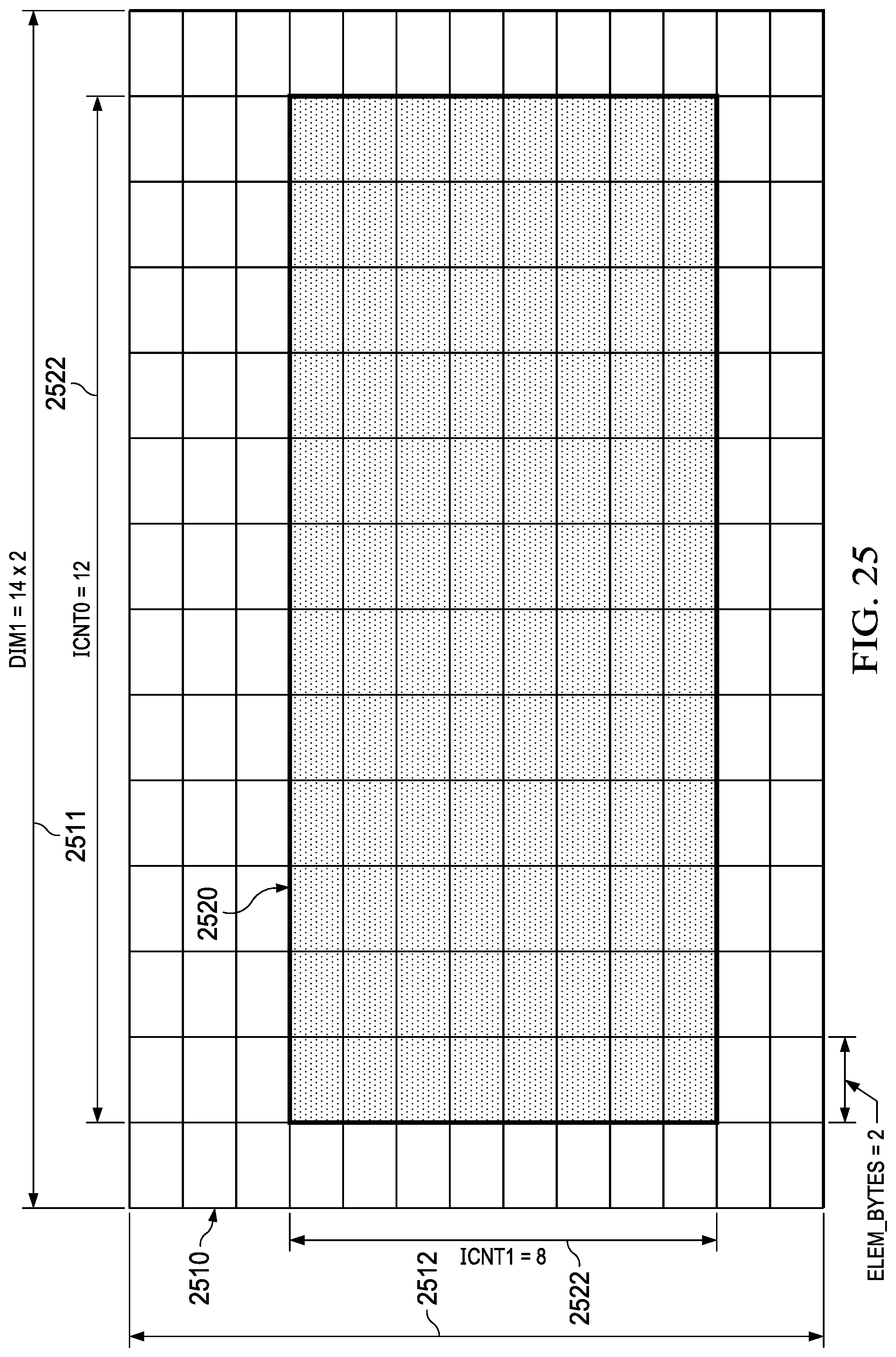
D00013
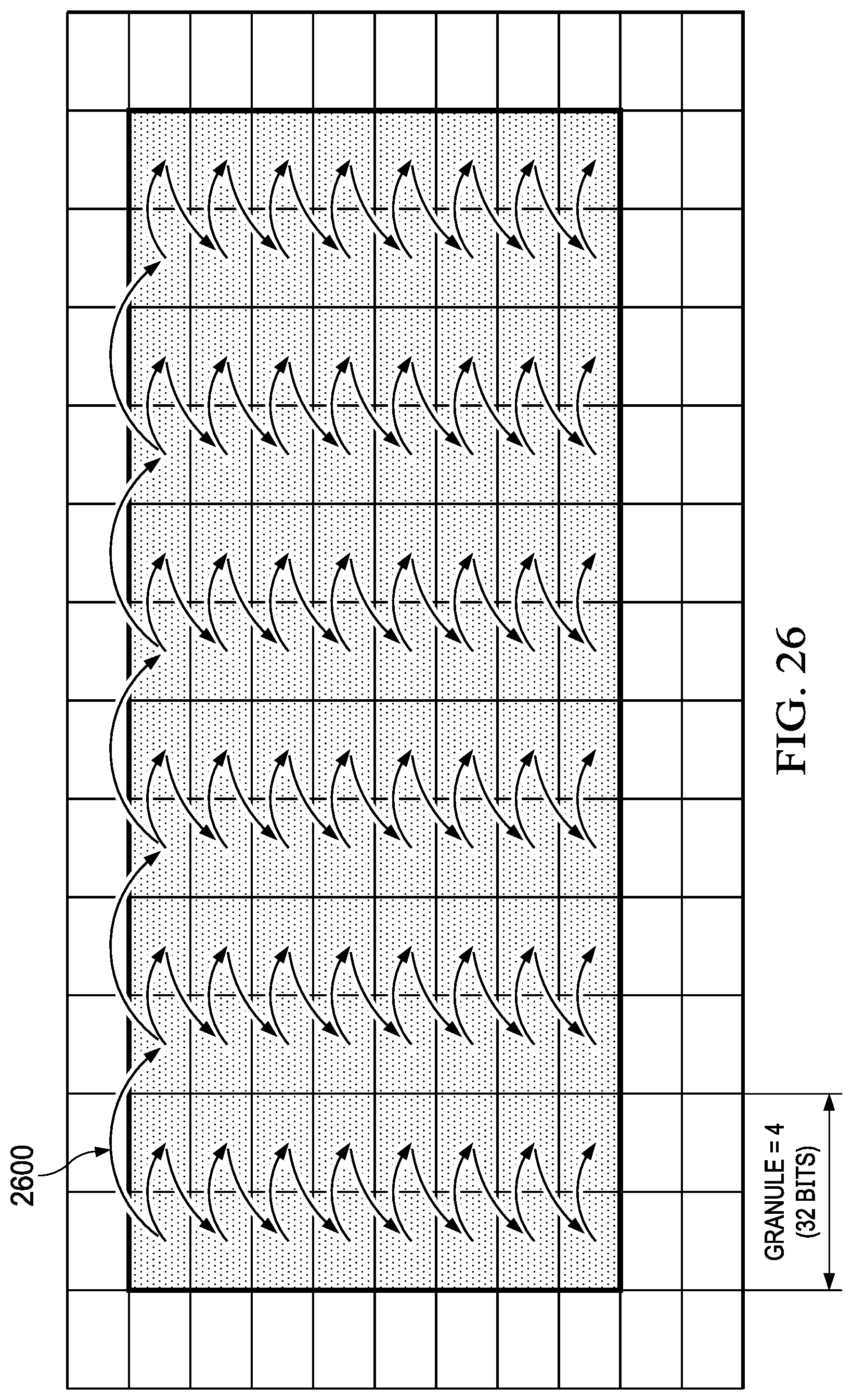
D00014
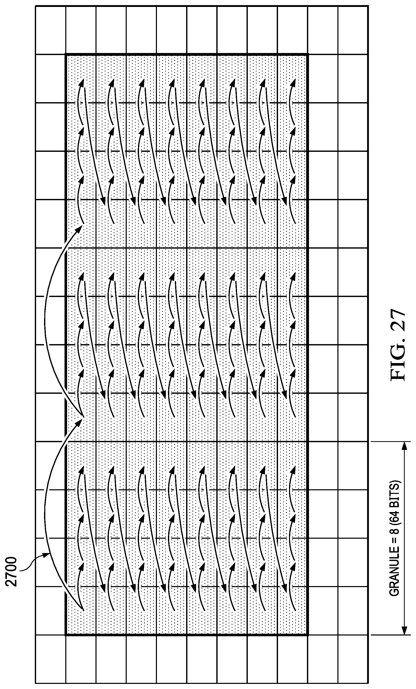
D00015

D00016

D00017

D00018
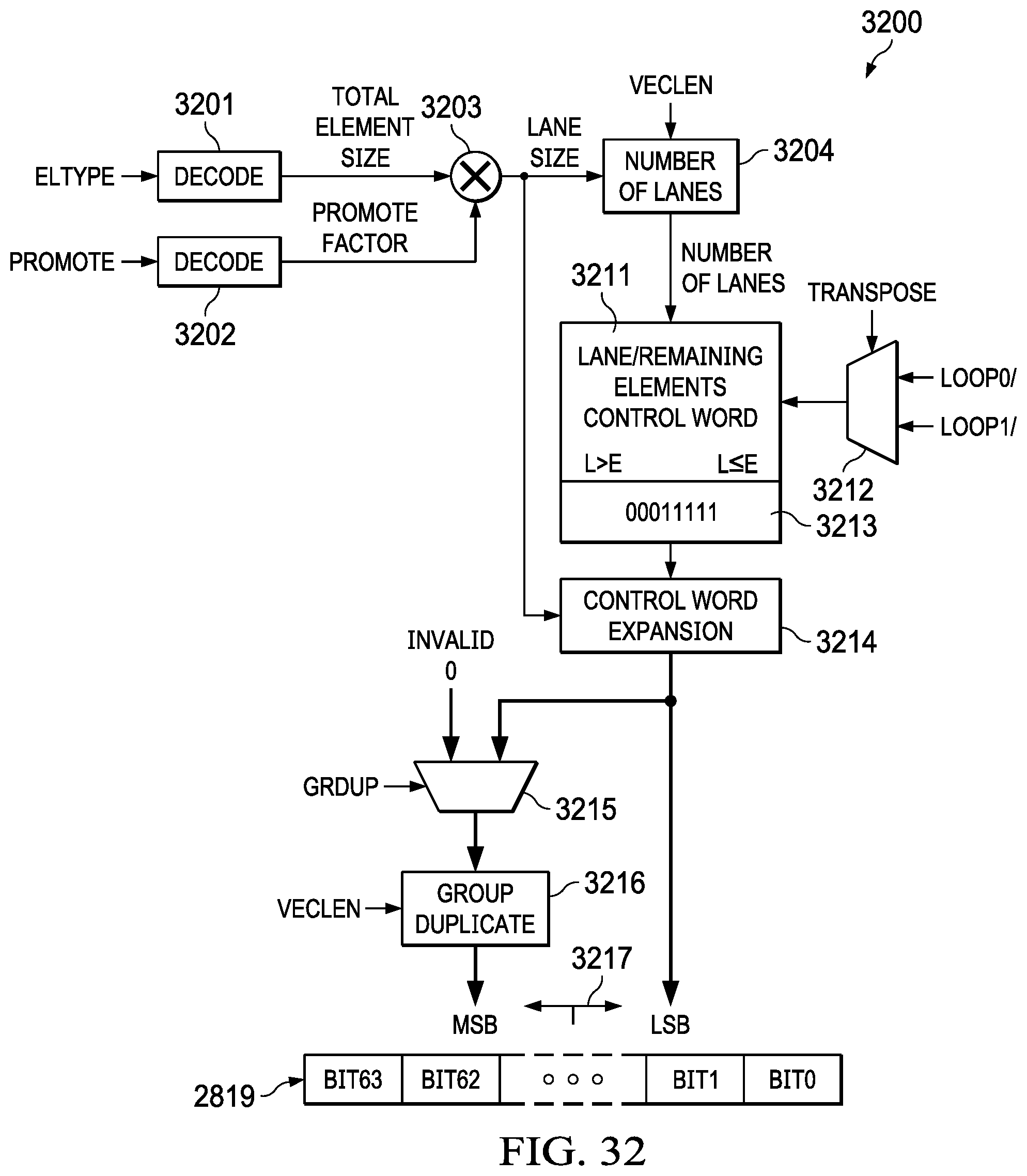
D00019

D00020

D00021
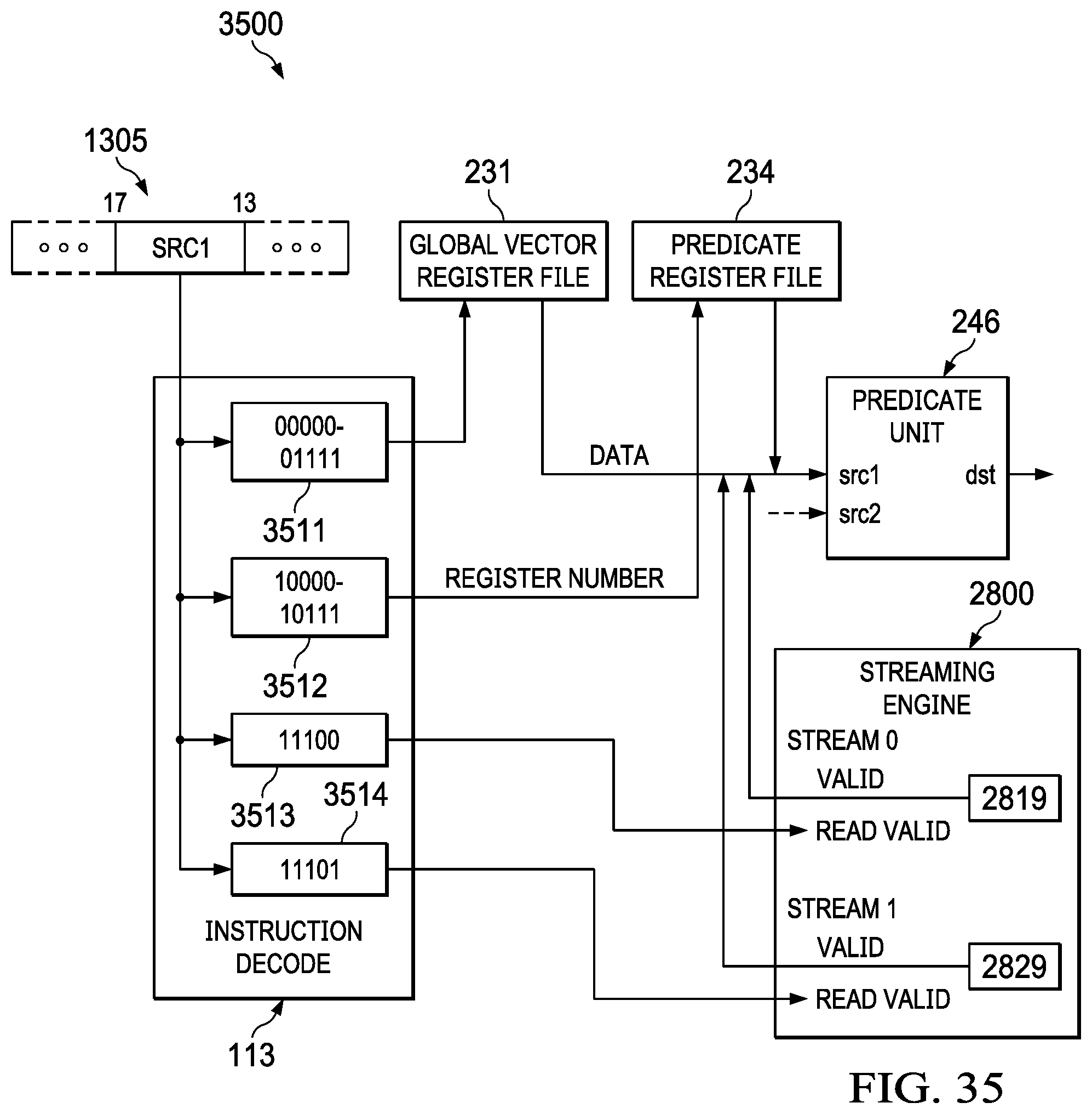
D00022

D00023
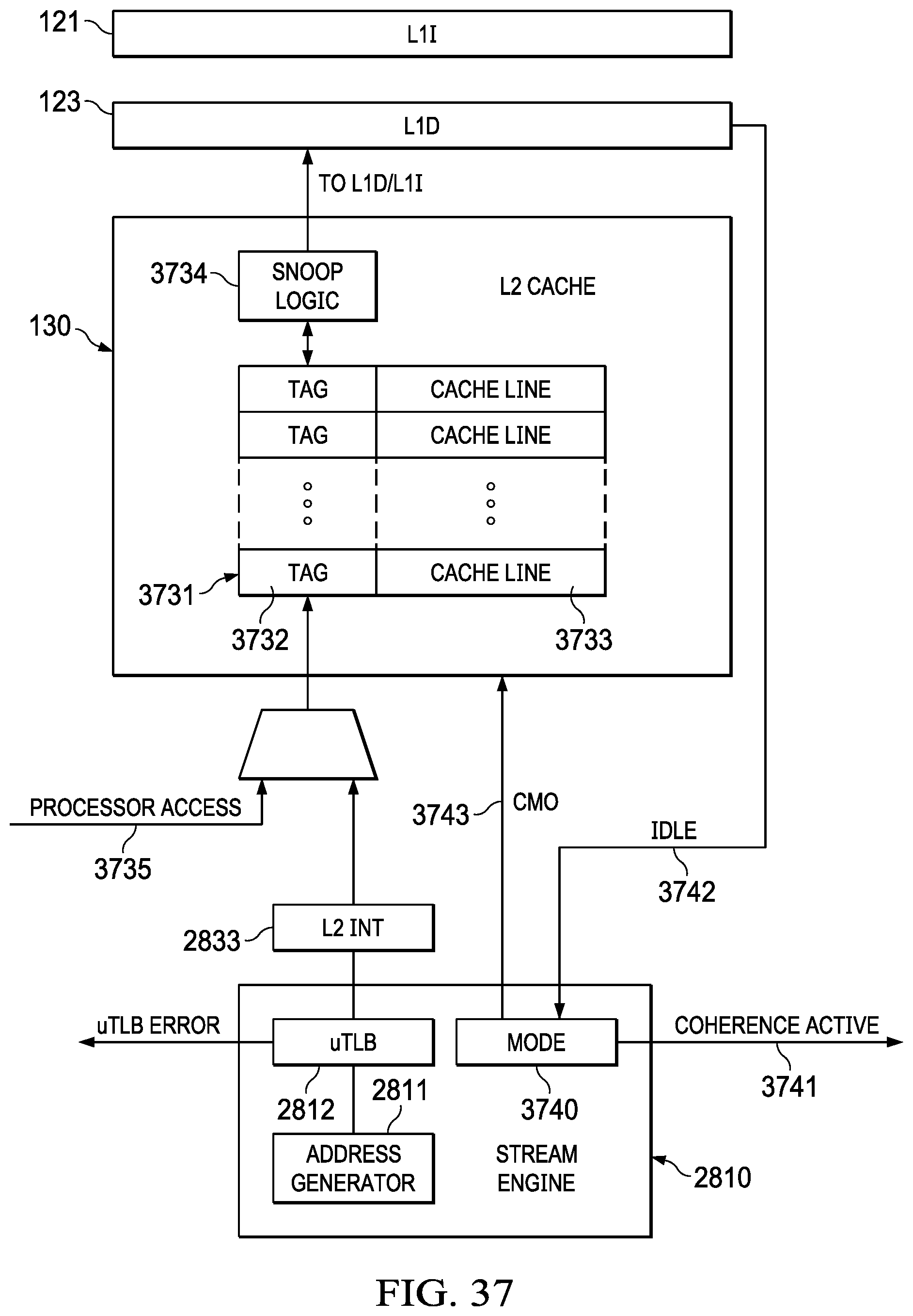
D00024
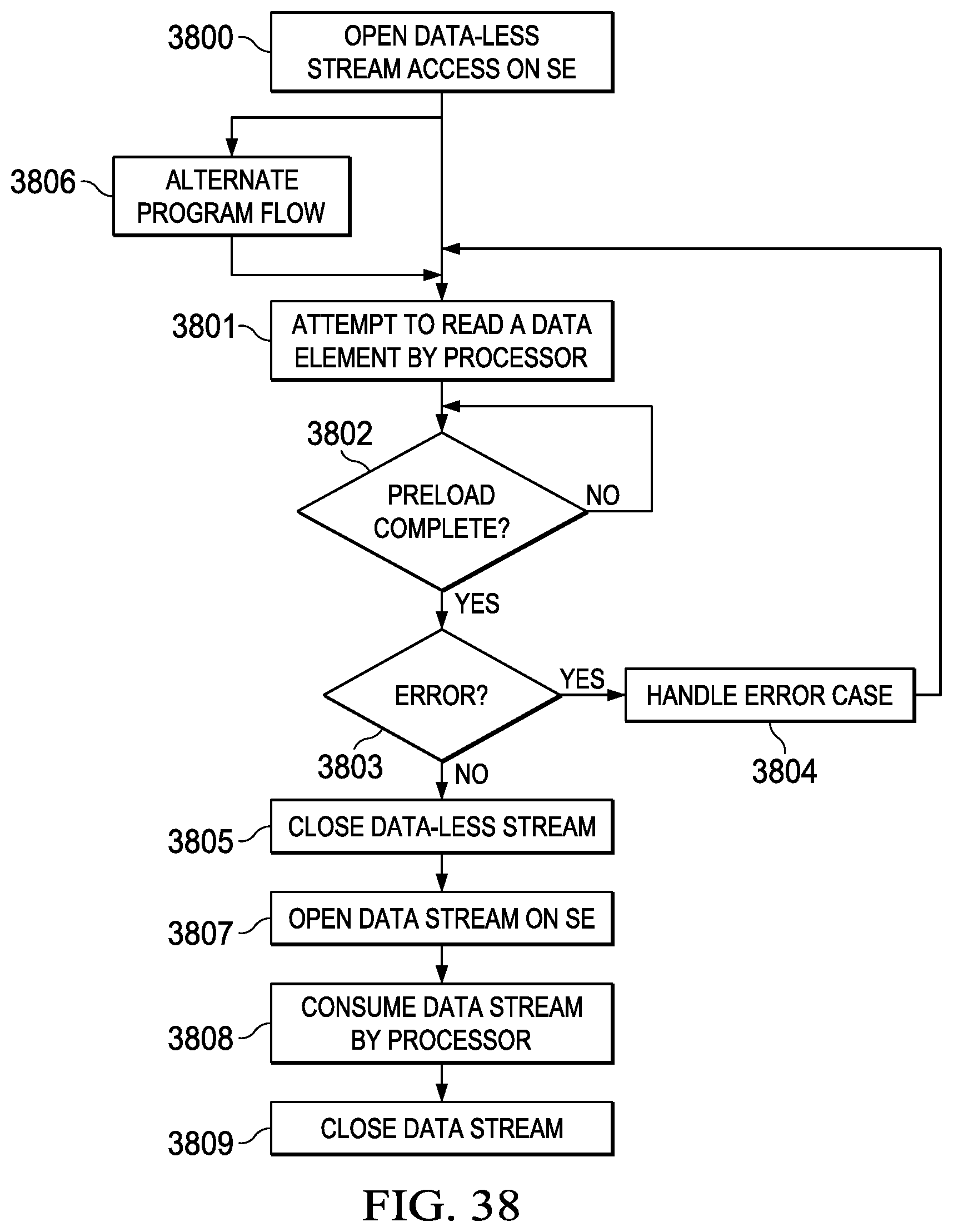
XML
uspto.report is an independent third-party trademark research tool that is not affiliated, endorsed, or sponsored by the United States Patent and Trademark Office (USPTO) or any other governmental organization. The information provided by uspto.report is based on publicly available data at the time of writing and is intended for informational purposes only.
While we strive to provide accurate and up-to-date information, we do not guarantee the accuracy, completeness, reliability, or suitability of the information displayed on this site. The use of this site is at your own risk. Any reliance you place on such information is therefore strictly at your own risk.
All official trademark data, including owner information, should be verified by visiting the official USPTO website at www.uspto.gov. This site is not intended to replace professional legal advice and should not be used as a substitute for consulting with a legal professional who is knowledgeable about trademark law.