Power module for supporting high current densities
Henning , et al. June 1, 2
U.S. patent number 11,024,731 [Application Number 16/171,521] was granted by the patent office on 2021-06-01 for power module for supporting high current densities. This patent grant is currently assigned to Cree, Inc.. The grantee listed for this patent is Cree, Inc.. Invention is credited to Anant Kumar Agarwal, Scott Allen, Jason Patrick Henning, John Williams Palmour, Sei-Hyung Ryu, Qingchun Zhang.


View All Diagrams
| United States Patent | 11,024,731 |
| Henning , et al. | June 1, 2021 |
Power module for supporting high current densities
Abstract
A power module is disclosed that includes a housing with an interior chamber wherein multiple switch modules are mounted within the interior chamber. The switch modules comprise multiple transistors and diodes that are interconnected to facilitate switching power to a load. In one embodiment, at least one of the switch modules supports a current density of at least 10 amperes per cm.sup.2.
| Inventors: | Henning; Jason Patrick (Carrboro, NC), Zhang; Qingchun (Cary, NC), Ryu; Sei-Hyung (Cary, NC), Agarwal; Anant Kumar (Chapel Hill, NC), Palmour; John Williams (Cary, NC), Allen; Scott (Apex, NC) | ||||||||||
|---|---|---|---|---|---|---|---|---|---|---|---|
| Applicant: |
|
||||||||||
| Assignee: | Cree, Inc. (Durham,
NC) |
||||||||||
| Family ID: | 1000005591403 | ||||||||||
| Appl. No.: | 16/171,521 | ||||||||||
| Filed: | October 26, 2018 |
Prior Publication Data
| Document Identifier | Publication Date | |
|---|---|---|
| US 20190067468 A1 | Feb 28, 2019 | |
Related U.S. Patent Documents
| Application Number | Filing Date | Patent Number | Issue Date | ||
|---|---|---|---|---|---|
| 15482936 | Apr 10, 2017 | 10153364 | |||
| 13588329 | Jun 6, 2017 | 9673283 | |||
| 61533254 | Sep 11, 2011 | ||||
| Current U.S. Class: | 1/1 |
| Current CPC Class: | H01L 27/0629 (20130101); H01L 29/7806 (20130101); H01L 21/049 (20130101); H01L 29/7805 (20130101); H01L 29/1608 (20130101); H01L 29/7802 (20130101); H01L 25/18 (20130101); H01L 29/0696 (20130101); H01L 21/046 (20130101); H01L 29/7395 (20130101); H01L 29/66068 (20130101); H01L 29/045 (20130101); H01L 2924/13091 (20130101); H02M 7/003 (20130101); H02P 7/04 (20160201); H01L 2924/0002 (20130101); H01L 2924/0002 (20130101); H01L 2924/00 (20130101); H01L 2924/13091 (20130101); H01L 2924/00 (20130101) |
| Current International Class: | H01L 29/78 (20060101); H01L 29/16 (20060101); H01L 29/739 (20060101); H01L 29/06 (20060101); H01L 21/04 (20060101); H01L 25/18 (20060101); H01L 27/06 (20060101); H02P 7/03 (20160101); H02M 7/00 (20060101); H01L 29/04 (20060101); H01L 29/66 (20060101) |
References Cited [Referenced By]
U.S. Patent Documents
| 3439189 | April 1969 | Petry |
| 3629011 | December 1971 | Tohi et al. |
| 3924024 | December 1975 | Naber et al. |
| 4160920 | July 1979 | Courier de Mere |
| 4242690 | December 1980 | Temple |
| 4466172 | August 1984 | Batra |
| 4581542 | April 1986 | Steigerald |
| 4644637 | February 1987 | Temple |
| 4811065 | March 1989 | Cogan |
| 4875083 | October 1989 | Palmour |
| 4927772 | May 1990 | Arthur et al. |
| 4945394 | July 1990 | Palmour et al. |
| 4946547 | August 1990 | Palmour et al. |
| 5005462 | April 1991 | Jasper, Jr. et al. |
| 5011549 | April 1991 | Kong et al. |
| 5028977 | July 1991 | Kenneth et al. |
| 5032888 | July 1991 | Seki |
| 5111253 | May 1992 | Korman et al. |
| 5155289 | October 1992 | Bowles |
| 5168139 | December 1992 | Bettge et al. |
| 5170231 | December 1992 | Fujii et al. |
| 5170455 | December 1992 | Goossen et al. |
| 5184199 | February 1993 | Fujii et al. |
| 5192987 | March 1993 | Khan et al. |
| 5200022 | April 1993 | Kong et al. |
| 5210051 | May 1993 | Carter, Jr. |
| 5270554 | December 1993 | Palmour |
| 5292501 | March 1994 | Degenhardt et al. |
| 5296395 | March 1994 | Khan et al. |
| 5348895 | September 1994 | Smayling et al. |
| 5371383 | December 1994 | Miyata et al. |
| 5384270 | January 1995 | Ueno et al. |
| 5385855 | January 1995 | Brown et al. |
| RE34861 | February 1995 | Davis et al. |
| 5393993 | February 1995 | Edmond et al. |
| 5393999 | February 1995 | Malhi |
| 5396085 | March 1995 | Baliga |
| 5459107 | October 1995 | Palmour |
| 5468654 | November 1995 | Harada |
| 5479316 | December 1995 | Smrtic et al. |
| 5488236 | January 1996 | Baliga et al. |
| 5506421 | April 1996 | Palmour |
| 5510281 | April 1996 | Ghezzo et al. |
| 5510630 | April 1996 | Agarwal et al. |
| 5523589 | June 1996 | Edmond et al. |
| 5539217 | July 1996 | Edmond et al. |
| 5545905 | August 1996 | Muraoka et al. |
| 5587870 | December 1996 | Anderson et al. |
| 5629531 | May 1997 | Palmour |
| 5703383 | December 1997 | Nakayama |
| 5710059 | January 1998 | Rottner |
| 5726463 | March 1998 | Brown et al. |
| 5726469 | March 1998 | Chen |
| 5734180 | March 1998 | Malhi |
| 5739564 | April 1998 | Kosa et al. |
| 5763905 | June 1998 | Harris |
| 5776837 | July 1998 | Palmour |
| 5804483 | September 1998 | Harris |
| 5808451 | September 1998 | Endou et al. |
| 5814859 | September 1998 | Ghezzo et al. |
| 5831288 | November 1998 | Singh et al. |
| 5837572 | November 1998 | Gardner et al. |
| 5851908 | December 1998 | Harris et al. |
| 5877041 | March 1999 | Fuller |
| 5877045 | March 1999 | Kapoor |
| 5885870 | March 1999 | Maiti et al. |
| 5914500 | June 1999 | Bakowski et al. |
| 5917203 | June 1999 | Bhatnagar et al. |
| 5917204 | June 1999 | Bhatnagar et al. |
| 5939763 | August 1999 | Hao et al. |
| 5960289 | September 1999 | Tsui et al. |
| 5969378 | October 1999 | Singh |
| 5972801 | October 1999 | Lipkin et al. |
| 5976936 | November 1999 | Miyajima et al. |
| 5977605 | November 1999 | Bakowsky et al. |
| 6002159 | December 1999 | Bakowski et al. |
| 6020600 | February 2000 | Miyajima et al. |
| 6025233 | February 2000 | Terasawa |
| 6025608 | February 2000 | Harris et al. |
| 6028012 | February 2000 | Wang |
| 6040237 | March 2000 | Bakowski et al. |
| 6048766 | April 2000 | Gardner et al. |
| 6054352 | April 2000 | Ueno |
| 6054728 | April 2000 | Harada et al. |
| 6063698 | May 2000 | Tseng et al. |
| 6083814 | July 2000 | Nilsson et al. |
| 6091108 | July 2000 | Harris et al. |
| 6096607 | August 2000 | Ueno |
| 6100169 | August 2000 | Suvorov et al. |
| 6104043 | August 2000 | Hermansson et al. |
| 6107142 | August 2000 | Suvorov et al. |
| 6117735 | September 2000 | Ueno |
| 6121633 | September 2000 | Singh et al. |
| 6133587 | October 2000 | Takeuchi et al. |
| 6136727 | October 2000 | Ueno |
| 6136728 | October 2000 | Wang |
| 6165822 | December 2000 | Okuno et al. |
| 6180958 | January 2001 | Cooper, Jr. |
| 6190973 | February 2001 | Berg et al. |
| 6204135 | March 2001 | Peters et al. |
| 6204203 | March 2001 | Narwankar et al. |
| 6211035 | April 2001 | Moise et al. |
| 6218254 | April 2001 | Singh et al. |
| 6218680 | April 2001 | Carter, Jr. et al. |
| 6221700 | April 2001 | Okuno et al. |
| 6228720 | May 2001 | Kitabatake et al. |
| 6238967 | May 2001 | Shiho et al. |
| 6239463 | May 2001 | Williams et al. |
| 6239466 | May 2001 | Elasser et al. |
| 6246076 | June 2001 | Lipkin et al. |
| 6252258 | June 2001 | Chang et al. |
| 6252288 | June 2001 | Chang |
| 6297100 | October 2001 | Kumar et al. |
| 6297172 | October 2001 | Kashiwagi |
| 6303508 | October 2001 | Alok |
| 6310775 | October 2001 | Nagatomo et al. |
| 6316791 | November 2001 | Schorner et al. |
| 6316793 | November 2001 | Sheppard et al. |
| 6329675 | December 2001 | Singh et al. |
| 6344663 | February 2002 | Slater, Jr. et al. |
| 6344676 | February 2002 | Yun et al. |
| 6365462 | April 2002 | Baliga |
| 6365932 | April 2002 | Kouno et al. |
| 6388271 | May 2002 | Mitlehner et al. |
| 6399996 | June 2002 | Chang et al. |
| 6420225 | July 2002 | Chang et al. |
| 6429041 | August 2002 | Ryu et al. |
| 6448160 | September 2002 | Chang et al. |
| 6455892 | September 2002 | Okuno et al. |
| 6475889 | November 2002 | Ring |
| 6515303 | February 2003 | Ring |
| 6524900 | February 2003 | Dahlqvist et al. |
| 6534367 | March 2003 | Peake et al. |
| 6548333 | April 2003 | Smith |
| 6551865 | April 2003 | Kumar et al. |
| 6573534 | June 2003 | Kumar et al. |
| 6593620 | July 2003 | Hshieh et al. |
| 6610366 | August 2003 | Lipkin |
| 6627539 | September 2003 | Zhao et al. |
| 6649497 | November 2003 | Ring |
| 6653659 | November 2003 | Ryu et al. |
| 6696705 | February 2004 | Barthelmess et al. |
| 6703642 | March 2004 | Shah |
| 6743703 | June 2004 | Rodov et al. |
| 6767843 | July 2004 | Lipkin et al. |
| 6861723 | March 2005 | Willmeroth |
| 6936850 | August 2005 | Friedrichs et al. |
| 6946739 | September 2005 | Ring |
| 6956238 | October 2005 | Ryu et al. |
| 6974720 | December 2005 | Sumakeris et al. |
| 6979863 | December 2005 | Ryu |
| 7026650 | April 2006 | Ryu et al. |
| 7074643 | July 2006 | Ryu |
| 7118970 | October 2006 | Das et al. |
| 7125786 | October 2006 | Ring et al. |
| 7221010 | May 2007 | Ryu |
| 7230275 | June 2007 | Kumar et al. |
| 7253031 | August 2007 | Takahashi et al. |
| 7276747 | October 2007 | Loechelt et al. |
| 7279115 | October 2007 | Sumakeris |
| 7304363 | December 2007 | Shah |
| 7365363 | April 2008 | Kojima et al. |
| 7381992 | June 2008 | Ryu |
| 7407837 | August 2008 | Tsuji |
| 7425757 | September 2008 | Takubo |
| 7498633 | March 2009 | Cooper et al. |
| 7528040 | May 2009 | Das et al. |
| 7544963 | June 2009 | Saxler |
| 7548112 | June 2009 | Sheppard |
| 7649213 | January 2010 | Hatakeyama et al. |
| 7687825 | March 2010 | Zhang |
| 7728402 | June 2010 | Zhang et al. |
| 7829402 | November 2010 | Matocha et al. |
| 7855384 | December 2010 | Yamamoto |
| 7855464 | December 2010 | Shikano |
| 8035112 | October 2011 | Cooper et al. |
| 8541787 | September 2013 | Zhang |
| 9029945 | May 2015 | Ryu et al. |
| 9142662 | September 2015 | Ryu et al. |
| 9373617 | June 2016 | Das et al. |
| 9640617 | May 2017 | Das et al. |
| 9673283 | June 2017 | Henning |
| 2001/0011729 | August 2001 | Singh et al. |
| 2001/0033502 | October 2001 | Blair et al. |
| 2001/0050383 | December 2001 | Hatade et al. |
| 2001/0055852 | December 2001 | Moise et al. |
| 2002/0030191 | March 2002 | Das et al. |
| 2002/0038891 | April 2002 | Ryu et al. |
| 2002/0047125 | April 2002 | Fukuda et al. |
| 2002/0071293 | June 2002 | Eden et al. |
| 2002/0072247 | June 2002 | Lipkin et al. |
| 2002/0102358 | August 2002 | Das et al. |
| 2002/0121641 | September 2002 | Alok et al. |
| 2002/0125482 | September 2002 | Friedrichs et al. |
| 2002/0125541 | September 2002 | Korec et al. |
| 2002/0185679 | December 2002 | Baliga |
| 2003/0025175 | February 2003 | Asano et al. |
| 2003/0107041 | June 2003 | Tanimoto et al. |
| 2003/0137010 | July 2003 | Friedrichs et al. |
| 2003/0142513 | July 2003 | Vinciarelli |
| 2003/0178672 | September 2003 | Hatakeyama et al. |
| 2003/0201455 | October 2003 | Takahashi et al. |
| 2004/0016929 | January 2004 | Nakatsuka et al. |
| 2004/0041229 | March 2004 | Chol et al. |
| 2004/0082116 | April 2004 | Kub et al. |
| 2004/0183079 | September 2004 | Kaneko et al. |
| 2004/0207968 | October 2004 | Martin et al. |
| 2004/0211980 | October 2004 | Ryu |
| 2004/0212011 | October 2004 | Ryu |
| 2004/0227231 | November 2004 | Maly et al. |
| 2004/0256659 | December 2004 | Kim et al. |
| 2004/0259339 | December 2004 | Tanabe et al. |
| 2005/0012143 | January 2005 | Tanaka et al. |
| 2005/0035364 | February 2005 | Sano et al. |
| 2005/0104072 | May 2005 | Slater, Jr. et al. |
| 2005/0139936 | June 2005 | Li |
| 2005/0151138 | July 2005 | Slater, Jr. et al. |
| 2005/0152100 | July 2005 | Rodriguez et al. |
| 2005/0181536 | August 2005 | Tsuji |
| 2005/0230686 | October 2005 | Kojima et al. |
| 2005/0275055 | December 2005 | Parthasarathy et al. |
| 2006/0011128 | January 2006 | Ellison et al. |
| 2006/0055027 | March 2006 | Kitabatake et al. |
| 2006/0060884 | March 2006 | Ohyanagi et al. |
| 2006/0071295 | April 2006 | Chang |
| 2006/0086997 | April 2006 | Kanaya et al. |
| 2006/0108589 | May 2006 | Fukuda et al. |
| 2006/0170835 | August 2006 | Jun et al. |
| 2006/0211210 | September 2006 | Bhat et al. |
| 2006/0216896 | September 2006 | Saito et al. |
| 2006/0244010 | November 2006 | Saxler |
| 2006/0255423 | November 2006 | Ryu et al. |
| 2006/0261347 | November 2006 | Ryu et al. |
| 2006/0261876 | November 2006 | Agarwal et al. |
| 2006/0267021 | November 2006 | Rowland et al. |
| 2006/0270103 | November 2006 | Das et al. |
| 2007/0066039 | March 2007 | Agarwal et al. |
| 2007/0090415 | April 2007 | Ronsisvalle |
| 2007/0096081 | May 2007 | Sugawara |
| 2007/0114606 | May 2007 | Hoshino et al. |
| 2007/0120148 | May 2007 | Nogome |
| 2007/0164321 | July 2007 | Sheppard et al. |
| 2007/0170436 | July 2007 | Sugawara |
| 2007/0241427 | October 2007 | Mochizuki et al. |
| 2007/0262324 | November 2007 | Kaneko |
| 2008/0001158 | January 2008 | Das et al. |
| 2008/0006848 | January 2008 | Chen et al. |
| 2008/0029838 | February 2008 | Zhang et al. |
| 2008/0048258 | February 2008 | de Fresart et al. |
| 2008/0105949 | May 2008 | Zhang |
| 2008/0191304 | August 2008 | Zhang et al. |
| 2008/0224316 | September 2008 | Kroeninger et al. |
| 2008/0230787 | September 2008 | Suzuki et al. |
| 2008/0251793 | October 2008 | Mazzola et al. |
| 2008/0258252 | October 2008 | Shimizu et al. |
| 2008/0277669 | November 2008 | Okuno et al. |
| 2008/0296771 | December 2008 | Das et al. |
| 2009/0008709 | January 2009 | Yedinak et al. |
| 2009/0039498 | February 2009 | Bayerer |
| 2009/0095979 | April 2009 | Saito et al. |
| 2009/0101918 | April 2009 | Uchida et al. |
| 2009/0121319 | May 2009 | Zhang et al. |
| 2009/0146154 | June 2009 | Zhang et al. |
| 2009/0168471 | July 2009 | Tsugawa et al. |
| 2009/0212301 | August 2009 | Zhang et al. |
| 2009/0225578 | September 2009 | Kitabatake |
| 2009/0272982 | November 2009 | Nakamura et al. |
| 2009/0289262 | November 2009 | Zhang et al. |
| 2009/0321746 | December 2009 | Harada et al. |
| 2010/0032685 | February 2010 | Zhang et al. |
| 2010/0127371 | May 2010 | Tschirbs |
| 2010/0127652 | May 2010 | Morita et al. |
| 2010/0133549 | June 2010 | Zhang et al. |
| 2010/0133550 | June 2010 | Zhang et al. |
| 2010/0140628 | June 2010 | Zhang |
| 2010/0163888 | July 2010 | Saggio et al. |
| 2010/0227515 | September 2010 | VanSlembrouck et al. |
| 2010/0244047 | September 2010 | Hull et al. |
| 2010/0295062 | November 2010 | Uchida et al. |
| 2010/0301335 | December 2010 | Ryu |
| 2011/0012132 | January 2011 | Otsuka |
| 2011/0018004 | January 2011 | Shimizu et al. |
| 2011/0018040 | January 2011 | Smith et al. |
| 2011/0058293 | March 2011 | Pardoen et al. |
| 2011/0101375 | May 2011 | Zhang |
| 2011/0128707 | June 2011 | Rozman et al. |
| 2011/0193412 | August 2011 | Lacarnoy |
| 2011/0199792 | August 2011 | Friebe et al. |
| 2011/0246794 | October 2011 | Liao |
| 2011/0292617 | December 2011 | Darroman et al. |
| 2011/0317729 | December 2011 | Matsumoto et al. |
| 2012/0012861 | January 2012 | Nakano |
| 2012/0025263 | February 2012 | Yamaguchi |
| 2012/0044720 | February 2012 | Shea et al. |
| 2012/0248094 | October 2012 | Strotmann et al. |
| 2012/0292636 | November 2012 | Zhang |
| 2013/0000170 | January 2013 | Dueck et al. |
| 2013/0001703 | January 2013 | Sugawara |
| 2013/0016542 | January 2013 | Nakamura et al. |
| 2013/0056755 | March 2013 | Hatai et al. |
| 2013/0083485 | April 2013 | Tong et al. |
| 2013/0207123 | August 2013 | Henning et al. |
| 2013/0248883 | September 2013 | Das et al. |
| 2013/0307500 | November 2013 | Nojiri et al. |
| 2014/0246681 | September 2014 | Das et al. |
| 2015/0214205 | July 2015 | Tokuyama et al. |
| 2016/0204101 | July 2016 | Das et al. |
| 2017/0213811 | July 2017 | Das et al. |
| 3942640 | Aug 1990 | DE | |||
| 19809554 | Sep 1998 | DE | |||
| 19832329 | Feb 1999 | DE | |||
| 19900171 | Jul 1999 | DE | |||
| 19817444 | Sep 1999 | DE | |||
| 10036208 | Feb 2002 | DE | |||
| 0176778 | Apr 1986 | EP | |||
| 0372412 | Jun 1990 | EP | |||
| 0389863 | Oct 1990 | EP | |||
| 0637069 | Feb 1995 | EP | |||
| 0837508 | Apr 1996 | EP | |||
| 0735591 | Oct 1996 | EP | |||
| 0865085 | Sep 1998 | EP | |||
| 1058317 | Dec 2000 | EP | |||
| 1361614 | Nov 2003 | EP | |||
| 1460681 | Sep 2004 | EP | |||
| 1503425 | Feb 2005 | EP | |||
| 1693896 | Aug 2006 | EP | |||
| 1806787 | Jul 2007 | EP | |||
| 1845561 | Oct 2007 | EP | |||
| 2015364 | Jan 2009 | EP | |||
| 2124257 | Nov 2009 | EP | |||
| 2432014 | Mar 2012 | EP | |||
| 60240158 | Nov 1985 | JP | |||
| 1117363 | May 1989 | JP | |||
| 03034466 | Feb 1991 | JP | |||
| 03157974 | Jul 1991 | JP | |||
| 3225870 | Oct 1991 | JP | |||
| 08264766 | Oct 1996 | JP | |||
| H08340103 | Dec 1996 | JP | |||
| 09205202 | Aug 1997 | JP | |||
| H10290562 | Oct 1998 | JP | |||
| 11191559 | Jul 1999 | JP | |||
| 11238742 | Aug 1999 | JP | |||
| 11261061 | Sep 1999 | JP | |||
| 11266017 | Sep 1999 | JP | |||
| 11274487 | Oct 1999 | JP | |||
| 2000049167 | Feb 2000 | JP | |||
| 2000082812 | Mar 2000 | JP | |||
| 2000106371 | Apr 2000 | JP | |||
| 2000252461 | Sep 2000 | JP | |||
| 2000252478 | Sep 2000 | JP | |||
| 2002314099 | Oct 2002 | JP | |||
| 2004363328 | Dec 2004 | JP | |||
| 2007234722 | Sep 2007 | JP | |||
| 2007258742 | Oct 2007 | JP | |||
| 2008277400 | Nov 2008 | JP | |||
| 2010010505 | Jan 2010 | JP | |||
| WO 20140/110246 | Mar 2010 | JP | |||
| 2010183840 | Aug 2010 | JP | |||
| 2011030424 | Feb 2011 | JP | |||
| 2012156548 | Aug 2012 | JP | |||
| 9603774 | Feb 1996 | WO | |||
| 9708754 | Mar 1997 | WO | |||
| 9717730 | May 1997 | WO | |||
| 9739485 | Oct 1997 | WO | |||
| 9802916 | Jan 1998 | WO | |||
| 9802924 | Jan 1998 | WO | |||
| 9808259 | Feb 1998 | WO | |||
| 9832178 | Jul 1998 | WO | |||
| 9963591 | Dec 1999 | WO | |||
| 0013236 | Mar 2000 | WO | |||
| 0178134 | Oct 2001 | WO | |||
| 2004020706 | Mar 2004 | WO | |||
| 2004079789 | Sep 2004 | WO | |||
| 2005020308 | Mar 2005 | WO | |||
| 2006135031 | Dec 2006 | WO | |||
| 2007040710 | Apr 2007 | WO | |||
| 2009128382 | Oct 2009 | WO | |||
| 2010004715 | Jan 2010 | WO | |||
| 2010074275 | Jul 2010 | WO | |||
| 2013036370 | Mar 2013 | WO | |||
Other References
|
Notice of Reasons for Rejection for Japanese Patent Application No. 2016-567562, dated Feb. 5, 2019, 10 pages. cited by applicant . Advisory Action for U.S. Appl. No. 15/483,039, dated Jan. 10, 2019, 3 pages. cited by applicant . Minutes of Oral Proceedings for European Patent Application No. 12762112.6, mailed Jul. 30, 2019, 5 pages. cited by applicant . Decision to Refuse for European Patent Application No. 12762112.6, dated Jul. 31, 2019, 14 pages. cited by applicant . Notification of the Third Office Action for Chinese Patent Application No. 2015800376807, dated Jul. 15, 2019, 16 pages. cited by applicant . Decision of Rejection for Japanese Patent Application No. 2016-567562, dated Oct. 1, 2019, 9 pages. cited by applicant . Second Office Action for Chinese Patent Application No. 2015800376807, dated Mar. 8, 2019, 14 pages. cited by applicant . Intention to Grant for European Patent Application No. 14730035.4, dated Oct. 12, 2020, 7 pages. cited by applicant . International Preliminary Report on Patentability for International Application No. PCT/US2012/051429, dated Mar. 20, 2014, 9 pages. cited by applicant . Non-Final Office Action for U.S. Appl. No. 13/588,329, dated Apr. 22, 2014, 21 pages. cited by applicant . International Search Report and Written Opinion for PCT/US2014/037977, dated Sep. 15, 2014, 11 pages. cited by applicant . Non-Final Office Action for U.S. Appl. No. 13/588,329, dated Sep. 24, 2014, 16 pages. cited by applicant . Berning, David W. et al., "High-Voltage Isolated Gate Drive Circuit for 10 kV, 100 A SiC MOSFET/JBS Power Modules," IEEE Industry Applications Society Annual Meeting, Oct. 5-9, 2008, IEEE, pp. 1-7. cited by applicant . Grider David et al., "10kV/120 A SiC DMOSFET Half H-Bridge Power Modules for 1 MVA Solid State Power Substation," IEEE Electric Ship Technologies Symposium (ESTS), Apr. 10-13, 2011, IEEE, pp. 131-134. cited by applicant . Mauch, Daniel et al., "High Power Lateral Silicon Carbide Photoconductive Semiconductor Switches and Investigation of Degradation Mechanisms," IEEE Transactions on Plasma Science, vol. 43, Issue 6, Jun. 2015, IEEE, pp. 2021-2031. cited by applicant . Moran, S.L. et al., "Hydrogen spark switches for rep-rated accelerators," 9th International Conference on High-Power Particle Beams, May 25-29, 1992, IEEE, 1 page, Abstract. cited by applicant . Rognlien, S., "Electric power supply with rectifier installation for the Alnor aluminum works at Karmoy," Elektroteknisk Tidsskrift, vol. 81, Issue 20, Oct. 17, 1968, Oslo, Ingeniorforlaget, 1 page, Abstract. cited by applicant . Wang, Jun et al., "Characterization, Modeling, and Application of 10-kV SiC MOSFET," IEEE Transactions on Electron Devices, vol. 55, Issue 8, Aug. 2008, IEEE, pp. 1798-1806. cited by applicant . Yu, Lei et al., "Design of 150 kV all-solid-state high voltage pulsed power generator," High Power Laser and Particle Beams, vol. 24, Issue 3, Mar. 2012, Nuclear Society of China, 1 page, Abstract. cited by applicant . Zorngiebel, Volker et al., "Modular 50-kV IGBT Switch for Pulsed-Power Applications," IEEE Transactions on Plasma Science, vol. 39, Issue 1, Jan. 2011, IEEE, pp. 364-367. cited by applicant . Second Office Action for Chinese Patent Application No. 201280055081.4, dated Nov. 8, 2016, 20 pages. cited by applicant . Third Office Action for Chinese Patent Application No. 201280055081.4, dated Apr. 1, 2017, 19 pages. cited by applicant . Report of Reexamination before Appeal for Japanese Patent Application No. 2014-529750, mailed Aug. 18, 2016, 6 pages. cited by applicant . Decision on Appeal for Japanese Patent Application No. 2014-529750, mailed May 10, 2017, 41 pages. cited by applicant . International Preliminary Report on Patentability for International Patent Application No. PCT/US2015/030853, dated Nov. 24, 2016, 10 pages. cited by applicant . Non-Final Office Action for U.S. Appl. No. 13/588,329, dated Jun. 27, 2016, 19 pages. cited by applicant . Notice of Allowance for U.S. Appl. No. 13/588,329, dated Dec. 23, 2016, 10 pages. cited by applicant . Corrected Notice of Allowability for U.S. Appl. No. 13/588,329, dated Jan. 25, 2017, 7 pages. cited by applicant . Corrected Notice of Allowability for U.S. Appl. No. 13/588,329, dated Mar. 13, 2017, 7 pages. cited by applicant . Corrected Notice of Allowability for U.S. Appl. No. 13/588,329, dated May 8, 2017, 6 pages. cited by applicant . Examination Report for European Patent Application No. 12762112.6, dated Feb. 1, 2017, 4 pages. cited by applicant . Advisory Action for U.S. Appl. No. 13/893,998, dated Aug. 31, 2016, 3 pages. cited by applicant . Notice of Allowance for U.S. Appl. No. 13/893,998, dated Dec. 15, 2016, 9 pages. cited by applicant . Notice of Allowability for U.S. Appl. No. 13/893,998, dated Jan. 10, 2017, 6 pages. cited by applicant . Corrected Notice of Allowability for U.S. Appl. No. 13/893,998, dated Jan. 25, 2017, 6 pages. cited by applicant . Corrected Notice of Allowability for U.S. Appl. No. 13/893,998, dated Feb. 16, 2017, 6 pages. cited by applicant . Corrected Notice of Allowability for U.S. Appl. No. 13/893,998, dated Mar. 14, 2017, 6 pages. cited by applicant . Corrected Notice of Allowability and Response to Rule 312 Communication for U.S. Appl. No. 13/893,998 dated Mar. 30, 2017, 7 pages. cited by applicant . Afanasev, V. et al., "Intrinsic SiC/SiO2 Interface States", Phys. Stat. Sol., Jan. 31, 1997, vol. 162, pp. 321-337. cited by applicant . Agarwal et al., "9kV, 1xcm SiC Super GTO Technology Development for Pulse Power," Pulsed Power Conference, 2009, presented Jun. 28-Jul. 2, 2009, pp. 264-269. cited by applicant . Agarwal, A.K. et al., "700-V Assymetrical 4H-SiC Gate Turn-Off Thyristors (GTO's)," IEEE Electron Device Letters, vol. 18, No. 11, Nov. 1997, pp. 518-520. cited by applicant . Agarwal, A.K. et al., "1.1 kV 4H-SiC Power UMOSFETs", IEEE Electron Devices Letters, Dec. 1997, vol. 18, No. 12, pp. 586-588. cited by applicant . Agarwal, A.K. et al., "1400 V 4H-SiC Power MOSFETs", Materials Science Forum, Jan. 1998, vols. 264-268, pp. 989-992. cited by applicant . Agarwal, A.K. et al., "A Critical Look at the Performance Advantages and Limitations of 4H-SiC Power UMOSFET Structures", Proceedings of the International Symposium on Power Semiconductor Devices and IC's, May 20-23, 1996, pp. 119-122. cited by applicant . Agarwal, A.K. et al., "Investigation of Lateral RESURF, 6H-SiC MOSFETs", Materials Science Forum, Copyright: 2000, vols. 338-342, pp. 1307-1310. cited by applicant . Agarwal, A.K. et al., "Temperature Dependence of Fowler-Nordheim Current in 6H- and 4H-SiC MOS Capacitors", IEEE Electron Device Letters, Dec. 1997, vol. 18, No. 12, pp. 592-594. cited by applicant . Alok, Dev. et al., "Process Dependence of Inversion Layer Mobility in 4H-SiC Devices", Silicon Carbide and Related Materials, Oct. 10-15, 1999, pp. 1077-1080. cited by applicant . Asano, K. et al., "Dynamic Characteristics of 6.2 kV High Voltage 4H-SiC pn Diode with Low Loss", Transactions of be Institute of Electrical Engineers of Japan, May 2003, vol. 123-D, No. 5, pp. 623-627. cited by applicant . Author Unknown, "Definition of Overlap," The American Heritage Dictionary of the English Language, Fourth Edition, Sep. 2003, 3 pages, http://www.thefreedictionary.com/overlap. cited by applicant . Author Unknown, "Insulated-Gate Bipolar Transistor," Wikipedia--The Free Encyclopedia, Jun. 21, 2010, 6 pages, http://en.wikipedia.org/wiki/Insulated-gate_bipolar_transistor. cited by applicant . Author Unknown, "Motorola Power MOSFET Transistor Databook", 4th Edition, Motorola, Inc., Copyright: 1989, pp. 254-257. cited by applicant . Author Unknown, "The Insulated Gate Biopolar Transistor (IGBT)", University of Glasgow, Updated: Feb. 14, 2007, Retrieved Jul. 7, 2006, http://www.elec.gla.ac.uk/groups/dev_mod/papers/igbt/igbt.html. cited by applicant . Ayalew, T., "4.43.1 MPS Diode Structure", Tu Wien. Jul. 6, 2006, http://www.iue.tuwien.ac.at/phd/ayalew/node88.html. cited by applicant . Baliga, B., "Chapter 7: Power Mosfet", Power Semiconductor Devices, May 2, 1995, pp. 335-425, Boston, MA, PWS Publishing Company. cited by applicant . Baliga, B., "Chapter 8: Insulated Gate Bipolar Transistor", Power Semiconductor Devices, May 2, 1995, pp. 426-502, Boston, MA, PWS Publishing Company. cited by applicant . Bhatnagar et al., "Comparison of 6H-SiC, 3C-SiC, and Si for power devices," Transactions on Electron Devices, vol. 40, No. 3, Mar. 1993, pp. 645-655. cited by applicant . Buchner, R. et al., "Laser Recrystallization of Polysilicon for Improved Device Quality", Springer Proceedings in Physics, Copyright: 1989, vol. 55, pp. 289-294. cited by applicant . Capano, M.A. et al., "Ionization Energies and Electron Mobilities in Phosphorus- and Nitrogen-Implanted 4H Silicon Carbide", IEEE ICSCRM Conference 1999, Oct. 10-13, 1999, 4 pages. cited by applicant . Capano, M.A. et al., "Surface Roughening in Ion Implanted 4-H Silicon Carbide", Journal of Electronic Materials, Jul. 20, 1998, vol. 28, No. 3, pp. 214-218. cited by applicant . Casady, J.B. et al., "900 V DMOS and 1100 V UMOS 4H-SiC Power FETs", Northrop Grumman Science and Technology Center, Published: 1997, 2 Pages. cited by applicant . Chakraborty, Supratic et al., "Interface Properties of N2O-Annealed SiO2/SiC System", 2008 IEEE Proceedings of the Electron Devices Meeting, Dec. 15-17, 2000, pp. 108-111, Hong Kong. cited by applicant . Chang, H.R. et al., "500-V n-Channel Insulated-Gate Bipolar Transistor with a Trench Gate Structure," IEEE Transactions on Electron Devices, vol. 36, No. 9, Sep. 1989, pp. 1824-1829. cited by applicant . Chang, K.C. et al., "Observation of a Non-Stoichiometric Layer at the Silicon Dioxide--Silicon Carbide Interface: Effect of Oxidation Temperature and Post-Oxidation Processing Conditions", Materials Research Social Symposium Procedures, vol. 640, Nov. 29-Dec. 2, 2011, 6 pages. cited by applicant . Chen, Jia-Rong et al., "Theoretical Analysis of Current Crowding Effect in Metal/AlGaN/GaN Schottky Diodes and its Reduction by Using Polysilicon in Anode", Chinese Physics Letters, Jul. 2007, vol. 24, No. 7, pp. 2112-2114. cited by applicant . Cho, Won-Ju et al., "Improvement of Charge Trapping by Hydrogen Post-Oxidation Annealing in Gate Oxide of 4H-SiC metal-oxide-semiconductor capacitors", Applied Physical Letters, Aug. 21, 2000, vol. 77, No. 8, 1215-1217. cited by applicant . Chung, G.Y. et al., "The Effect of Si:C Source Ratio on S102 /SiC Interface State Density for Nitrogen Doped 4H and 6H SiC", Materials Science Forum, Copyright: 2000, vol. 338-342, pp. 1097-1100. cited by applicant . Chung, G.Y. et al., "Effect of Nitric Oxide Annealing on the Interface Trap Densities Near the Band Edges in the 4H Polytype Silicon Carbide", Applied Physics Letters, Mar. 27, 2000, vol. 76, No. 13, pp. 1713-1715. cited by applicant . Chung, G.Y. et al., "Improved Inversion Channel Mobility for 4h-SiC MOSFETs Following High Temperature Anneals in Nitric Oxide", IEEE Electron Device Letters, Apr. 2001, vol. 22, No. 4, pp. 176-178. cited by applicant . Chung, Gilyong et al., "Effects of Anneals in Ammonia on the Interface Trap Density Near the Band Edges in 4H-Silicon Carbide Metal-Oxide-Semiconductor Capacitors", Applied Physical Letters, Nov. 27, 2000, vol. 77, No. 22, pp. 3601-3603. cited by applicant . Dahlquist, F. et al., "A 2.8kV, Forward Drop JBS Diode with Low Leakage", Materials Science Forum, Jan. 2000, vols. 338-342, pp. 1179-1182. cited by applicant . Das, M.K. et al., "High Mobility 4H-SiC Inversion Mode MOSFETs Using Thermally Grown", No Annealed SiO2,, IEEE 58th Device Research Conference, Jun. 19-21, 2000, 3 Pages. cited by applicant . Das, M.K. et al., "Inversion Channel Mobility in 4H- and 6H-SiC MOSFETs", School of Electrical and Computer Engineering at Purdue University, Published: 1998, 2 pages. cited by applicant . Das, Mrinal K. et al., "A 13 kV 4H-SiC n-Channel IGBT with Low Rdiff on and Fast Switching", DARPA Contract, Sep. 2008, 4 Pages. cited by applicant . Das, Mrinal K., "Fundamental Studies of the Silicon Carbide MOS Structure", Thesis submitted to Purdue University for Doctorate of Philosophy Program, Dec. 1999, 160 Pages. cited by applicant . Dastidar, Sujoyita, "A Study of P-Type Activation in Silicon Carbide", Thesis submitted to Faculty of Purdue University, May 1998, 102 Pages. cited by applicant . De Meo, R.C. et al., "Thermal Oxidation of SiC in N2O", The Electrochemical Society, Inc., Nov. 1994, vol. 141, No. 11, pp. L150-L152. cited by applicant . Del Prado, A. et al., "Full Composition Range Silicon Oxynitride Films Deposited by ECR-PECVD at Room Temperature", Thin Solid Films, Apr. 1999, vols. 343-344, pp. 437-440. cited by applicant . Dimitrijev, Sima et al., "Nitridation of Silicon-Dioxide Films Grown on 6H Silicon Carbide", IEEE Electron Device Letters, May 1997, vol. 18, No. 5, pp. 175-177. cited by applicant . Fisher, C.A. et al., "The Performance of High-Voltage Field Relieved Schottky Barrier Diodes", IEE Proceedings, Dec. 1985, vol. 132, Pt. 1, No. 6, pp. 257-260. cited by applicant . Fukuda, Kenji et al., "Improvement of SiO2/4H-SiC Interface by Using High Temperature Hydrogen Annealing at 1000.degree. C.", External Abstracts of the 1998 International Conference on Solid State Devices and Materials, Published: 1998, pp. 100-101. cited by applicant . Fukuda, Kenji et al., "Improvement of SiO2/4H-SiC Interface Using High-Temperature Hydrogen Annealing at Low Pressure and Vacuum Annealing", Japanese Journal of Applied Physics, Apr. 1999, vol. 38, pp. 2306-2309. cited by applicant . Hubel, Kerstin, "Hybrid Design Improves Diode Robustness and Boosts Efficiency", Compound Semiconductor. Net, Updated: May 2006, Retrieved: Jul. 7, 2006, http://www.compoundsemiconductor.net. cited by applicant . Hull, Brett A. et al., "Drift-Free 10-kV, 20-A 4H-SiC PiN Diodes", Journal of Electronic Materials, Apr. 2005, vol. 34, No. 4, pp. 341-344. cited by applicant . Jamet, P. et al., "Physical Properties of N/sub 2/0 and No--Nitrided Fate Oxides Grown on 4H SiC", Applied Physics Letters, Jul. 2001, vol. 79, No. 3, pp. 323-325. cited by applicant . Kinoshita, Kozo et al., "Guard Ring Assisted RESURF: A New Termination Structure Providing Stable and High Breakdown Voltage for SiC Power Devices", Proceedings of the 14th International Symposium on Power Semiconductor Devces and ICs, Jun. 7, 2002, pp. 253-256. cited by applicant . Kobayashi, K. et al., "Dielectric Breakdown and Current Conduction of Oxide/Nitride/Oxide Multi-Layer Structures", 1990 Symposium of VLSI Technology, Jun. 4-7, 1990, pp. 119-120. cited by applicant . Krishnaswami, Sumi et al., "High Temperature Characterization of 4H-SiC Bipolar Junction Transistors", Materials Science Forum, Jan. 1, 2009, vols. 527-529, pp. 1437-1440. cited by applicant . Lai, P.T. et al., "Effects of Nitridation and Annealing on Interface Properties of Thermally Oxidized SlO2 /SiC Metal-Oxide-Semiconductor System", Applied Physics Letters, Jun. 19, 2000, vol. 75, No. 25, pp. 3744-3748. cited by applicant . Hull, B.A., et al., "1700V, 20A 4H-SiC DMOSFETs Optimized for High Temperature Operation," Materials Science Forum, vols. 679-680, Jan. 1, 2011, Trans Tech Publications, pp. 633-636. cited by applicant . Qingxin, X., "Frequency Converter Maintenance Quick Start," China Electric Power Press, Jan. 1, 2013, 6 pages. cited by applicant . Summons to Attend Oral Proceedings for European Patent Application No. 14730035.4, mailed Feb. 12, 2020, 12 pages. cited by applicant . Notification of the Fourth Office Action for Chinese Patent Application No. 2015800376807, dated Jan. 21, 2020, 8 pages. cited by applicant . Non-Final Office Action for U.S. Appl. No. 15/483,039, dated Apr. 9, 2020, 15 pages. cited by applicant . Hull, Brett A. et al., "Performance of 60 A, 1200 V 4H-Sic DMOSFETs," Materials Science Forum, vol. 315-617, 2009, Trans Tech Publications, pp. 749-752. cited by applicant . Kazuhiro, I. et al., "Simultaneous Formation of Ni/Al Ohmic Contacts to Both n- and p-Type 4H-SiC," Journal of Electronic Materials, vol. 37, No. 11, 2008, TMS, pp. 1674-1680. cited by applicant . First Office Action and Search Report for Chinese Patent Application No. 201280055081.4, dated Feb. 1, 2016, 31 pages. cited by applicant . Decision of Rejection for Japanese Patent Application No. 2014-529750, dated Feb. 26, 2016, 6 pages. cited by applicant . Extended European Search Report for European Patent Application No. 12782360.7, dated Oct. 7, 2014, 7 pages. cited by applicant . Office Action for Japanese Patent Application No. 2014-509288, dated Nov. 25, 2014, 10 pages. cited by applicant . Reason for Rejection for Japanese Patent Application No. 2014-529750, dated Apr. 15, 2015, 8 pages. cited by applicant . International Preliminary Report on Patentability for PCT/US2012/027255, dated Nov. 21, 2013, 7 pages. cited by applicant . International Preliminary Report on Patentability for PCT/US2014/037977, dated Nov. 26, 2015, 8 pages. cited by applicant . International Search Report and Written Opinion for No. PCT/US2015/030853, dated Nov. 5, 2015, 15 pages. cited by applicant . Final Office Action for U.S. Appl. No. 13/102,510, dated Nov. 29, 2013, 22 pages. cited by applicant . Advisory Action for U.S. Appl. No. 13/102,510, dated Feb. 6, 2014, 3 pages. cited by applicant . Non-Final Office Action for U.S. Appl. No. 13/102,510, dated Mar. 13, 2014, 10 pages. cited by applicant . Final Office Action for U.S. Appl. No. 13/102,510, dated Aug. 29, 2014, 9 pages. cited by applicant . Notice of Allowance for U.S. Appl. No. 13/102,510, dated Jan. 12, 2015, 9 pages. cited by applicant . Corrected Notice of Allowability for U.S. Appl. No. 13/102,510, dated Mar. 26, 2015, 4 pages. cited by applicant . Non-Final Office Action for U.S. Appl. No. 13/108,440, dated Dec. 30, 2013, 104 pages. cited by applicant . Final Office Action for U.S. Appl. No. 13/108,440, dated Jun. 24, 2014, 69 pages. cited by applicant . Non-Final Office Action for U.S. Appl. No. 13/108,440, dated Jan. 14, 2015, 10 pages. cited by applicant . Notice of Allowance for U.S. Appl. No. 13/108,440, dated Jun. 2, 2015, 16 pages. cited by applicant . Final Office Action for U.S. Appl. No. 13/588,329, dated Feb. 20, 2015, 18 pages. cited by applicant . Corrected Advisory Action for U.S. Appl. No. 13/588,329, dated Aug. 19, 2015, 3 pages. cited by applicant . Non-Final Office Action for U.S. Appl. No. 13/588,329, dated Feb. 3, 2016, 18 pages. cited by applicant . Non-Final Office Action for U.S. Appl. No. 13/893,998, dated Jan. 2, 2015, 7 pages. cited by applicant . Final Office Action for U.S. Appl. No. 13/893,998, dated May 19, 2015, 11 pages. cited by applicant . Advisory Action for U.S. Appl. No. 13/893,998, dated Jul. 29, 2015, 3 pages. cited by applicant . Non-Final Office Action for U.S. Appl. No. 13/893,998, dated Jan. 4, 2016, 12 pages. cited by applicant . Final Office Action for U.S. Appl. No. 13/893,998, dated May 17, 2016, 12 pages. cited by applicant . Non-Final Office Action for U.S. Appl. No. 14/277,820, dated Jun. 16, 2015, 13 pages. cited by applicant . Notice of Allowance for U.S. Appl. No. 14/277,820, dated Nov. 27, 2015, 9 pages. cited by applicant . Notice of Allowance for U.S. Appl. No. 14/277,820, dated May 25, 2016, 6 pages. cited by applicant . Das, Mrinal K., et al., "State of the Art 10 kV NMOS Transistors," Proceedings of the 20th International Symposium on Power Semiconductor Devices & IC's, May 18-22, 2008, Orlando, Florida, USA, pp. 253-255. cited by applicant . Summons to Attend Oral Proceedings for European Patent Application No. 12762112.6, mailed Oct. 12, 2018, 6 pages. cited by applicant . Examination Report for European Patent Application No. 14730035.4, dated Jun. 28, 2018, 9 pages. cited by applicant . First Office Action for Chinese Patent Application No. 2015800376807, dated Jun. 5, 2018, 7 pages. cited by applicant . Office Action for German Patent Application No. 112015002272.4, dated Sep. 12, 2018, 13 pages. cited by applicant . Notice of Reasons for Rejection for Japanese Patent Application No. 2016-567562, dated Mar. 13, 2018, 8 pages. cited by applicant . Non-Final Office Action for U.S. Appl. No. 15/482,936, dated Feb. 23, 2018, 12 pages. cited by applicant . Notice of Allowance for U.S. Appl. No. 15/482,936, dated Jul. 23, 2018, 8 pages. cited by applicant . Corrected Notice of Allowability for U.S. Appl. No. 15/482,936, dated Sep. 11, 2018, 5 pages. cited by applicant . Corrected Notice of Allowability for U.S. Appl. No. 15/482,936, dated Nov. 13, 2018, 5 pages. cited by applicant . Non-Final Office Action for U.S. Appl. No. 15/483,039, dated Feb. 22, 2018, 22 pages. cited by applicant . Final Office Action for U.S. Appl. No. 15/483,039, dated Oct. 11, 2018, 23 pages. cited by applicant . Non-Final Office Action for U.S. Appl. No. 15/077,329, dated Oct. 2, 2017, 13 pages. cited by applicant . Notice of Allowance for U.S. Appl. No. 151077,329, dated Mar. 26, 2018, 8 pages. cited by applicant . Corrected Notice of Allowance for U.S. Appl. No. 15/077,329, dated Jun. 13, 2018, 5 pages. cited by applicant . Corrected Notice of Allowance for U.S. Appl. No. 15/077,329, dated Oct. 29, 2018, 5 pages. cited by applicant . Lai, P.T. et al., "Interface properties of N2O-Annealed NH3-Treated 6H-SiC MOS Capacitor", Proceedings of the IEEE Hong Kong Electron Devices Meeting, Jun. 26, 1999, pp. 46-49. cited by applicant . Leonhard et al. "Long Term Stability of Gate-Oxides on n- and P-Type Silicon Carbide Studied by Charge Injection Techniques," Materials Science Engineering, vol. 46, No. 1-3, Apr. 1997, pp. 263-266. cited by applicant . Levinshtein, Michael E. et al., "On the Homogeneity of the Turn-On Process in High-Voltage 4H-SiC Thyristors", Solid-State Electronics, Feb. 2005, vol. 49, pp. 233-237. cited by applicant . Li, H.F. et al., "Improving SiO2 Grown on P-Type 4H-SiC by NO Annealing", Materials Science Forum, Feb. 1998, vol. 264-268, pp. 869-872. cited by applicant . Li, Y. et al., "High-Voltage (3 kV) UMOSFETs in 4H-SiC", IEEE Transactions on Electron Devices, Jun. 2002, vol. 49, No. 6, pp. 972-975. cited by applicant . Lipkin, L.A. et al., "Low Interfaces State Density Oxides on P-Type SiC", Materials Science Forum, Jan. 1998, vols. 264-268, pp. 853-856. cited by applicant . Lipkin, Lori et al., "Challenges and State-of-the-Art of Oxides on SiC", Material Research Social Symposium Proceedings, Nov. 2000, vol. 640, pp. 89-98. cited by applicant . Lipkin, Lori et al., "Insulator Investigation on SiC for Improved Reliability", IEEE Transactions on Electron Devices, Mar. 1999, vol. 46, No. 3, pp. 525-532. cited by applicant . Losee, P.A. et al., "High-Voltage 4H-SiC PiN Rectifiers with Single-Implant, Multi-Zone JTE Termination", Proceedings for 2004 International Symposium on Power Semiconductor Devices & ICs, May 2004, pp. 301-304. cited by applicant . Losse, P.A. et al., "Degraded Blocking Performance of 4H-SiC Rectifiers Under High dV/dt Conditions", Proceedings for 17th International Symposium on Power Semiconductor Devices & ICs, May 23-26, 2005, pp. 1-4. cited by applicant . Ma, Y. et al., "Fixed and Trapped Charges at Oxide-Nitride-Oxide Heterostructure Interfaces Formed by Remote Plasma Enhanced Chemical Vapor Deposition", American Vacuum Society, Jul. 1993, vol. 11, No. 4, pp. 1533-1540. cited by applicant . Miura, Naruhisa et al., "Successful Development of 1.2 kV 4H-SiC MOSFETs with the Very Low On-Resistance of 5 m.OMEGA.m2," Proceedings of the 18th International Symposium on Power Semiconductor Devices & IC's, Jun. 4-8, 2006, 4 pages, Naples Italy. cited by applicant . Mondal, K. et al., "An Integrated 500-V Power DMOSFET/Antiparallel Rectifier Device with Improved Diode Reverse Recovery Characteristics", IEEE Electron Device Letters, Sep. 2002, vol. 23, No. 9, pp. 562-564. cited by applicant . Mutin, P. Hubert, "Control of the Composition and Structure of Silicon Oxycarbide and Oxynitride Glasses Derived from Polysiloxane Precursors", Journal of Sol-Gel Science and Technology, Mar. 1999, pp. 27-38. cited by applicant . Myer-Ward, R.L. et al., "Turning of Basal Plane Dislocations During Epitaxial Growth on 4 Off-Axis 4h-SiC", 7th European Conference on Silicon Carbide and Related Materials, Sep. 7-11, 2008, retrieved Jul. 1, 2009, http://escrm08.com/invited_presentations.html, Barcelona, Spain. cited by applicant . Palmour, J.W. et al., "SiC Device Technology: Remaining Issues", Diamond and Related Materials, Aug. 1997, vol. 5, pp. 1400-1404. cited by applicant . Palmour, John, "Silicon Carbide npnp Thyristors", NASA Tech Briefs. Updated: Dec. 1, 2000, Retrieved Sep. 2, 2010, http://www.techbriefs.com/component/content/article/7031. cited by applicant . Pankin, D. et al., "Electrical and Microstructural Properties of Highly Boron-Implantation Doped 6H-SiC", Journal of Applied Physics, Mar. 15, 2001, vol. 89, No. 6, pp. 3162-3167. cited by applicant . Pantelides, S.T. et al., "Atomic-Scale Engineering of the SiC-SiO2 Interface", Materials Science Forum, Oct. 1999, vols. 338-342, pp. 1133-1136. cited by applicant . Patel, R. et al., "Phosphorus-Implanted High-Voltage N+P 4H-SiC Junction Rectifiers", Proceedings of 1998 International Symposium on Power Semiconductor Devices & Ics, Jun. 1998, pp. 387-390. cited by applicant . Rao et al., "Al and N Ion Implantations in 6H-SiC," Inst. Phys. Conf. Ser. No. 142, Chapter 3, Jan. 1996, pp. 521-524. cited by applicant . Rao, Mulpuri V. et al., "P-N Junction Formation in 6H-SiC Acceptor Implantation into a N-Type Substrate", Nuclear Instructions and Mechanics in Physics Res., Dec. 1995, vol. 106, pp. 333-338. cited by applicant . Rao, Mulpuri V., "Maturing Ion-Implantation Technology and its Device Applications in SiC", Solid State Electronics, Feb. 2003, vol. 47, pp. 213-222. cited by applicant . Rao, S. et al., "Silane Overpressure Post-Implant Annealing of A1 Dopants in SiC: Cold Wall CVD Apparatus", Applied Surface Science, Mar. 2006, vol. 252, pp. 3837-3842. cited by applicant . Richmond, J.T. et al., "Hybrid 4H-SiC MOS Gated Transistor (MGT)", DARPA Contract #N00014-99-C-0377, Sep. 2002, 6 pages. cited by applicant . Ryu, Sei-Hyung et al., "27 m.OMEGA.-cm2, 1.6 kV Power DiMOSFETs in 4H-SiC", Proceedings of the 14th International Symposium on Power Semiconductor Devices & ICs 2002, ISPSD '02 Proceedings, Jun. 4-7, 2002, pp. 65-68, Santa Fe, NM. cited by applicant . Salem, T.E. et al., "High-Temperature High-Power Operation of a 100 A SiC DMOSFET Module," Twenty-Fourth Annual IEEE Applied Power Electronics Conference and Exposition, Feb. 2009, pp. 653-657. cited by applicant . Schorner, Reinhold et al., "Rugged Power MOSFETs in 6H-SiC with Blocking Capability up to 1800V", Silicon carbide and Related Materials, Jan. 2000, vols. 338-342, pp. 1295-1298. cited by applicant . Schorner, Reinhold et al., "Significantly Improved Performance of MOSFET's on Silicon Carbide Using the 15R-SiC Polytype", IEEE Electron Device Letters, May 1999, vol. 20, No. 3, pp. 241-244. cited by applicant . Senzaki, Junji et al., "Effects of Pyrogenic Reoxidation Annealing on Inversion Channel Mobility of 4H-SiC Metal-Oxide-Semiconductor Field-effect Transistor Fabricated on (1120) Face", The Japanese Society of Applied Physics, Nov. 15, 2001, vol. 40, pp. 1201-1203. cited by applicant . Shenoy, Jayarama N. et al., "High-Voltage Double-Implanted Power MOSFET's in 6H-SiC", IEEE Electron Device Letters, Mar. 1997, vol. 18, No. 3, pp. 93-95. cited by applicant . Shenoy, Praveen M. et al., "The Planar 6H-SiC Accufet: A New High-Voltage Power MOSFET Structure", IEEE Electron Device Letters, Sep. 1999, vol. 18, No. 12, pp. 589-591. cited by applicant . Singh, R. et al., "Planar Terminations in 4H-SIC Schottky Diodes with Low Leakage and High Yields", ISPSD '97, May 1997, pp. 157-160. cited by applicant . Singh, R. et al., "High Temperature, High Current, 4H-SiC Accu-DMOSFET", Silicon Carbide and Related Materials, Copyright: 2000, vols. 338-342, pp. 1271-1274. cited by applicant . Sridevan, S. et al., "Lateral N-Channel Inversion Mode 4H-SiC MOSFET'S", IEEE Electron Devices Letters, Jul. 1998, vol. 19, No. 7, pp. 228-230. cited by applicant . Sridevan, S. et al., "On the Presence of Aluminum in Thermally Grown Oxides on 6H-Silicon Carbide", IEEE Electron Devices Letters, Mar. 1996, vol. 17, No. 3, pp. 136-138. cited by applicant . Stengl, R. et al., "Variation of Lateral Doping--A New Concept to Avoid High Voltage Breakdown of Planar Junctions", Science Research Laboratories, Jan. 12, 1985, 4 pages. cited by applicant . Stengl, R. et al., "Variation of Lateral Doping as a Field Terminator for High-Voltage Power Devices", IEEE Transactions on Electron Devices, Mar. 1986, vol. ED-33, No. 3, pp. 426-428. cited by applicant . Streetman, Ben G., "Chapter 7: Bipolar Junction Transistors", Solid State Electronic Devices, Mar. 1980, pp. 228-284, Englewood Cliffs, NJ, Prentice-Hall, Inc. cited by applicant . Sugawara, Yoshitaka et al., "3.6 kV 4H-SiC JBS Diodes with Low RonS", Materials Science Forum: Silicon Carbide and Related Materials, Sep. 2000, vol. 338-342, pp. 1183-1186. cited by applicant . Sundaresan, Siddarth G. et al., "Ultra-Low Resistivity A1+ Implanted 4H-SiC Obtained by Microwave Annealing and a Protective Graphite Cap", Solid-State Electronics 52, Jan. 2008, pp. 140-145. cited by applicant . Suvorov, A.V. et al., "4H-Sic Self-Aligned Implant-Diffused Structure for Power DMOSFETs", Materials Science Forum, Jan. 2000, vols. 338-342, pp. 1275-1278. cited by applicant . Suzuki, Seiji et al., "Effect of Post-Oxidation-Annealing in Hydrogen on SiO2 /4H-SiC Interface", Materials Science Forums, Jan. 2000, vols. 338-342, pp. 1073-1076. cited by applicant . Sze, S.M., "Si-SiO2 MOS Diode", Physics of Semiconductor Devices, 2nd Edition, Jan. 1998, pp. 383-390, Korea, John Wiley & Sons, Inc. cited by applicant . Sze, S.M., "Chapter 5: Bipolar Transistor and Related Devices", Semiconductor Devices Physics and Technology, Jan. 2002, p. 130, United States of America, John Wiley & Sons, Inc. cited by applicant . Tamaki, Tomohiro et al., "Optimization of On-State and Switching Performances for 15-20-kV 4H-SiC IGBTs," IEEE Transactions on Electron Devices, vol. 55, No. 8, Aug. 2008, pp. 1920-1927. cited by applicant . Tan, J. et al., "High-Voltage Accumulation-Layer UMOSFET's in 4H-SiC", IEEE Electron Device Letters, Sep. 1998, vol. 49, No. 12, pp. 487-489. cited by applicant . Thomas, Chris et al., "Annealing of Ion Implantation Damage in SiC Using a Graphite Mask", Materials Research Society Symposium Proc., Apr. 1999, vol. 572, pp. 45-50. cited by applicant . Tobin, Philip et al., "Furnace Formation of Silicon Oxynitride Thin Dielectrics in Nitrous Oxide N2O: The Role of Nitric Oxide (NO)", Junior Applied Physics, Feb. 1, 1994, vol. 75, No. 3, pp. 1811-1817. cited by applicant . Tone, Kiyoshi et al., "4H-SiC Normally-Off Vertical Junction Field-Effect Transistor With High Current Density," IEEE Electron Device Letters, vol. 24, No. 7, Jul. 2003, pp. 463-465. cited by applicant . Final Office Action for U.S. Appl. No. 15/483,039, dated Sep. 24, 2020, 16 pages. cited by applicant . Treu, M. et al., "A Surge Current Stable and Avalanche Rugged SiC Merged pn Schottky Diode Blocking 600V Especially Suited for PFC Applications", Materials Science Forum: Silicon Carbide and Related Materials, Oct. 2006, vol. 527-539, pp. 1155-1158. cited by applicant . Ueno, Katsunori et al., "The Guard-Ring Termination for High-Voltage SiC Schottky Barrier Diodes", IEEE Electron Device Letters, Jul. 1995, vol. 16, No. 7, pp. 331-332. cited by applicant . Ueno, Katsunori et al., "4H-SiC MOSFET's Utilizing the H2 Surface Cleaning Technique", IEEE Electron Device Letters, Jul. 1998, vol. 19, No. 7, pp. 244-246. cited by applicant . Ueno, Katsunori et al., "Counter-Doped MOSFET's of 4H-SiC", IEEE Electron Device Letters, Dec. 1999, vol. 20, No. 12, pp. 624-626. cited by applicant . Vassilveski, K. et al., "High Voltage Silicon Carbide Schottky Diodes with Single Zone Junction Termination Extension", Materials Science Forum, Sep. 2007, pp. 873-876, Switzerland, Trans Tech Publications. cited by applicant . Vassilveski, K.V. et al., "Protection of Selectively Implanted and Patterned Silicon Carbide Surfaces with Graphite Capping Layer During Post-Implantation Annealing", Semiconductor Science and Technology, Feb. 3, 2005, pp. 271-278, Switzerland, Trans Tech Publications. cited by applicant . Vathulya, Vickram et al., "A Novel 6H-SiC Power DMOSFET with Implanted P-Well Spacer", IEEE Electron Device Letters, Jul. 1999, vol. 20, No. 7, pp. 354-356. cited by applicant . Vathulya, Vickram et al., "Characterization of Channel Mobility of Implanted SiC to Determine Polytype Suitability or the Power DIMOS Structure", Powerpoint Presentation at Lehigh University, Presented 1999, 26 total slides, 13 pages. cited by applicant . Wang, Xiewen W. et al., "High Temperature Characteristics of High-Quality SiC MIS Capacitors with O/N/O Gate Dielectric", IEEE Transactions on Electron Devices, Feb. 2000, vol. 47, No. 2, pp. 450-462. cited by applicant . Wang, Y. et al., "Accumulation-Mode SiC Power MOSFET Design Issues", Material Science Forum, Feb. 2000, vols. 338-342, pp. 1287-1290. cited by applicant . Williams, J.R. et al., "Passivation of the 4H-SiC/SiO2 Interface with Nitric Oxide", Materials Science Forum, Jan. 2002, vols. 389-393, pp. 967-972. cited by applicant . Xu, J.P. et al., "Improved Performance and Reliability of N20-Grown Oxynitride on 6H-SiC", IEEE Electron Device Letters, Jun. 2000, vol. 21, No. 6, pp. 298-300. cited by applicant . Yilmaz, Hamza, "Optimization and Surface Charge Sensitivity of High Voltage Blocking Structures with Shallow Junctions", IEEE Transactions on Electron Devices, Jul. 1991, vol. 38, No. 7, pp. 1666-1675. cited by applicant . Zhang, Qingchun at al., "A 10-K Monolithic Darlington Transistor with .beta.forced of 336 in 4H-SiC", Feb. 2009, IEEE Electron Device Letters, Feb. 2009, vol. 30, No. 2, pp. 142-144. cited by applicant . Zhang, Qingchun et al., "12 Kv 4H-SiC p-IGBTs with Record Low Specific On-Resistance", Materials Science Forum, Sep. 2008, vols. 600-603, 4 pages. cited by applicant . Zhang, Qingchun et al., "Design and Fabrications of High Voltage IGBTs on 4H-SiC", Power semiconductor devices and IC's, 2006 IEEE International Symposium, Jun. 4-8, 2006, pp. 1-4. cited by applicant . Office Action for Chinese Patent Application No. 2007800294605, dated Jan. 22, 2010, 7 pages. cited by applicant . European Search Report for European Patent Application No. 09177558.5, dated Feb. 22, 2010, 6 pages. cited by applicant . European Search Report for European Patent Application No. 07120038.0, dated Jun. 16, 2008, 7 pages. cited by applicant . European Search Report for European Patent Application No. 09163424.6, dated Apr. 9, 2010, 10 pages. cited by applicant . Extended European Search Report for European Patent Application No. 07112298.0, dated Feb. 18, 2009, 12 pages. cited by applicant . International Search Report and Written Opinion for International Patent Application No. PCT/US2012/051429 dated Nov. 22, 2012, 15 pages. cited by applicant . International Search Report for International Patent Application No. PCT/US01/30715 dated Jun. 5, 2002, 9 pages. cited by applicant . International Search Report for International Patent Application No. PCT/US01/42414, dated Apr. 23, 2002, 10 pages. cited by applicant . International Search Report for International Patent Application No. PCT/US02/11691, dated Dec. 17, 2002, 9 pages. cited by applicant . International Search Report for International Patent Application No. PCT/US2004/004982 dated Jul. 22, 2004, 9 pages. cited by applicant . International Search Report for International Patent Application No. PCT/US2010/025053, dated Jul. 2, 2010, 18 pages. cited by applicant . International Search Report and Written Opinion for International Patent Application No. PCT/US2012/27255 dated Jun. 13, 2012, 10 pages. cited by applicant . International Search Report and Written Opinion for International Patent Application No. PCT/US2007/0014139, dated Feb. 4, 2008, 15 pages. cited by applicant . International Search Report and Written Opinion for International Patent Application No. PCT/US2008/0008574, dated Sep. 26, 2008, 15 pages. cited by applicant . International Search Report and Written Opinion for International Patent Application No. PCT/US2008/0010538, dated Dec. 22, 2008, 13 pages. cited by applicant . International Search Report for International Patent Application No. PCT/US2009/0000734, dated Apr. 23, 2009, 13 pages. cited by applicant . International Search Report and Written Opinion for International Patent Application No. PCT/US2009/0003089, dated Aug. 20, 2009, 16 pages. cited by applicant . International Search Report and Written Opinion for International Patent Application No. PCT/US2009/0065251, dated Jun. 1, 2010, 14 pages. cited by applicant . International Search Report and Written Opinion for International Patent Application No. PCT/US2010/0020071, dated Mar. 26, 2010, 14 pages. cited by applicant . Invitation to Pay Additional Fee for International Patent Application No. PCT/US2007/0010192, dated Oct. 29, 2007, 10 pages. cited by applicant . International Search Report and Written Opinion for International Patent Application No. PCT/US2008/004239, dated Mar. 2, 2009, 11 pages. cited by applicant . International Search Report and Written Opinion for International Patent Application No. PCT/US2010/0026632, dated Oct. 8, 2010, 13 pages. cited by applicant . International Search Report and Written Opinion for International Patent Application No. PCT/US2010/0028612, dated Jun. 17, 2010, 9 pages. cited by applicant . International Search Report and Written Opinion for International Patent Application No. PCT/US2010/0035713, dated Jul. 27, 2010, 11 pages. cited by applicant . International Search Report and Written Opinion for International Patent Application No. PCT/US2010/0042075, dated Sep. 24, 2010, 12 pages. cited by applicant . Non-Final Office Action for U.S. Appl. No. 13/108,440, dated Aug. 2, 2012, 23 pages. cited by applicant . Non-Final Office Action for U.S. Appl. No. 13/102,510, dated Aug. 2, 2012, 32 pages. cited by applicant . Final Office Action for U.S. Appl. No. 13/108,440, dated Jan. 17, 2013, 36 pages. cited by applicant . Final Office Action for U.S. Appl. No. 13/102,510, dated Feb. 12, 2013, 27 pages. cited by applicant . Advisory Action for U.S. Appl. No. 13/108,440, dated Mar. 25, 2013, 4 pages. cited by applicant . Advisory Action for U.S. Appl. No. 13/102,510, dated Apr. 19, 2013, 3 pages. cited by applicant . Non-Final Office Action for U.S. Appl. No. 13/102,510, dated Jun. 20, 2013, 28 pages. cited by applicant . Restriction Requirement for U.S. Appl. No. 13/588,329, dated Aug. 26, 2013, 7 pages. cited by applicant . Advisory Action for U.S. Appl. No. 15/483,039, dated Nov. 25, 2020, 3 pages. cited by applicant . Non-Final Office Action for U.S. Appl. No. 15/483,039, dated Jan. 6, 2021, 14 pages. cited by applicant . Notice of Reasons for Rejection for Japanese Patent Application No. 2016-567562, dated Dec. 15, 2020, 15 pages. cited by applicant . Notice of Reasons for Rejection for Japanese Patent Application No. 2020-015417, dated Mar. 23, 2021, 11 pages. cited by applicant. |
Primary Examiner: Jahan; Bilkis
Attorney, Agent or Firm: Withrow & Terranova, P.L.L.C.
Parent Case Text
CROSS REFERENCE TO RELATED APPLICATIONS
This application is a continuation of U.S. patent application Ser. No. 15/482,936 filed on Apr. 10, 2017, now U.S. Pat. No. 10,153,364, which is a continuation of U.S. patent application Ser. No. 13/588,329 filed on Aug. 17, 2012, which issued as U.S. Pat. No. 9,673,283 on Jun. 6, 2017, which claims the benefit of U.S. provisional patent application No. 61/533,254 filed Sep. 11, 2011, the disclosures of which are incorporated herein by reference in their entireties. The present application is a continuation of U.S. patent application Ser. No. 15/482,936 filed on Apr. 10, 2017, now U.S. Pat. No. 10,153,364, which is a continuation of U.S. patent application Ser. No. 13/588,329 filed on Aug. 17, 2012, which issued as U.S. Pat. No. 9,673,283 on Jun. 6, 2017, which is related to U.S. Pat. No. 9,142,662 issued on Sep. 22, 2015, which is a continuation in part of U.S. Pat. No. 9,029,945 issued on May 12, 2015. The present application is related to U.S. Pat. No. 9,142,662 issued on Sep. 22, 2015, which is a continuation in part of U.S. Pat. No. 9,029,945 issued on May 12, 2015, the disclosures of which are incorporated herein by reference in their entireties.
Claims
What is claimed is:
1. A power module comprising: a housing with an interior chamber; and a plurality of switch modules mounted within the interior chamber and comprising at least two transistors wherein at least one of the two transistors comprises: a drift layer having a first conductivity type; a well region having a second conductivity type that is opposite the first conductivity type; a source region in the well region, the source region having the first conductivity type; a plurality of body contact regions that are interspersed between portions of the source region, the plurality of body contact regions having the second conductivity type in contact with the well region; and a source ohmic contact that overlaps the source region in a source contact area and that overlaps the plurality of body contact regions in a plurality of body contact region areas; wherein a ratio of a minimum dimension p1 of a body contact region area of the plurality of body contact region areas to a minimum dimension w1 of the well region is greater than 0.2.
2. The power module of claim 1 wherein the source ohmic contact completely overlaps the plurality of the body contact regions.
3. The power module of claim 1 wherein the power module further comprises a plurality of diodes interconnected to facilitate switching power to a load.
4. The power module of claim 3 wherein a diode of the plurality of diodes is an internal diode.
5. The power module of claim 3 wherein a diode of the plurality of diodes is an external diode.
6. The power module of claim 1 wherein a ratio of a minimum dimension n1 of the source contact area to the minimum dimension w1 of the well region is greater than 0.2.
7. The power module of claim 6 wherein the ratio of the minimum dimension n1 of the source contact area to the minimum dimension w1 of the well region is in a range of 0.2 to 1.
8. A power module comprising: a housing with an interior chamber; and a plurality of switch modules mounted within the interior chamber and comprising at least two transistors wherein at least one of the two transistors comprises: a drift layer having a first conductivity type; a well region having a second conductivity type that is opposite the first conductivity type; a source region in the well region, the source region having the first conductivity type; a body contact region having the second conductivity type in contact with the well region; and a source ohmic contact that overlaps the source region in a source contact area and that overlaps the body contact region in a body contact region area, wherein a ratio of a minimum dimension n1 of the source contact area to a minimum dimension w1 of the well region is greater than 0.2.
9. The power module of claim 8 wherein the power module further comprises a plurality of diodes interconnected to facilitate switching power to a load.
10. The power module of claim 9 wherein a diode of the plurality of diodes is an internal diode.
11. The power module of claim 9 wherein a diode of the plurality of diodes is an external diode.
12. The power module of claim 8 wherein the ratio of the minimum dimension n1 of the source contact area to the minimum dimension w1 of the well region is greater than about 0.3.
13. The power module of claim 8 wherein the ratio of the minimum dimension n1 of the source contact area to the minimum dimension w1 of the well region is greater than about 0.5.
14. The power module of claim 8 wherein the ratio of the minimum dimension n1 of the source contact region area to the minimum dimension w1 of the well region is in a range of 0.2 to 1.
15. A power module comprising a housing with an interior chamber; and a plurality of switch modules mounted within the interior chamber and comprising at least two transistors wherein at least one of the two transistors comprises: a drift layer having a first conductivity type; a well region having a second conductivity type that is opposite the first conductivity type; a source region in the well region, the source region having the first conductivity type; a body contact region having the second conductivity type in contact with the well region; and a source ohmic contact that overlaps the source region in a source contact area and that overlaps the body contact region in a body contact region area, wherein a ratio of a minimum dimension p1 of the body contact region area to a minimum dimension w1 of the well region is greater than 0.2.
16. The power module of claim 15 wherein the power module further comprises a plurality of diodes interconnected to facilitate switching power to a load.
17. The power module of claim 16 wherein a diode of the plurality of diodes is an internal diode.
18. The power module of claim 16 wherein a diode of the plurality of diodes is an external diode.
19. The power module of claim 15, wherein the ratio of the minimum dimension p1 of the body contact region area to the minimum dimension w1 of the well region is greater than about 0.3.
20. The power module of claim 15 wherein the ratio of the minimum dimension p1 of the body contact region area to the minimum dimension w1 of the well region is greater than about 0.5.
21. The power module of claim 15 wherein the ratio of the minimum dimension p1 of the body contact region area to the minimum dimension w1 of the well region is in a range of 0.2 to 1.
22. The power module of claim 1 wherein the ratio of the minimum dimension p1 of the body contact region area of the plurality of body contact region areas to the minimum dimension w1 of the well region is in a range of 0.2 to 1.
Description
FIELD OF THE DISCLOSURE
The present disclosure relates to electronic devices and in particular to power modules.
BACKGROUND
Power devices made with silicon carbide (SiC) are expected to show great advantages as compared to those on silicon for high speed, high power and/or high temperature applications due to the high critical field and wide band gap of SiC. For devices capable of blocking high voltages, such as voltages in excess of about 5 kV, it may be desirable to have bipolar operation to reduce the drift layer resistance via conductivity modulation resulting from injected minority carriers. However, one technical challenge for bipolar devices in silicon carbide is forward voltage degradation over time, possibly due to the presence of Basal Plane Dislocations (BPD) in single crystals of silicon carbide. Thus, unipolar devices such as SiC Schottky diodes and MOSFETs are typically used for high power applications, e.g., up to 10 kV or more.
SiC DMOSFET devices with a 10 kV blocking capability have been fabricated with a specific on-resistance of about 100 m.OMEGA..times.cm.sup.2. DMOSFET devices may exhibit very fast switching speeds of, for example, less than 100 ns, due to their majority carrier nature. However, as the desired blocking voltage of devices increases, for example up to 15 kV or more, the on-resistance of a MOSFET device may increase substantially, due to the corresponding increase in the drift layer thickness. This problem may be exacerbated at high temperatures due to bulk mobility reduction, which may result in excessive power dissipation.
With the progress of SiC crystal material growth, several approaches have been developed to mitigate BPD related problems. See, e.g., B. Hull, M. Das, J. Sumakeris, J. Richmond, and S. Krishinaswami, "Drift-Free 10-kV, 20-A 4H-SiC PiN Diodes", Journal of Electrical Materials, Vol. 34, No. 4, 2005, which is incorporated herein by reference in its entirety. These developments may enhance the development and/or potential applications of SiC bipolar devices such as thyristors, GTOs, etc. Even though thyristors and/or GTOs may offer low forward voltage drops, they may require bulky commutating circuits for the gate drive and protections. Accordingly, it may be desirable for a SiC bipolar device to have gate turn-off capability. Due to their superior on-state characteristics, reasonable switching speed, and/or excellent safe-operation-area (SOA), 4H-SiC insulated gate bipolar transistors (IGBTs) are becoming more suitable for power switching applications.
These devices are used in power modules, which operate to dynamically control large amounts of power through switching for motors, inverters, generators, and the like. There is a continuing need for power modules that are smaller and less expensive to manufacture while at the same time being capable of controlling larger loads.
SUMMARY
A power module is disclosed that supports high current densities. The power module includes a housing with an interior chamber wherein multiple switch modules are mounted within the interior chamber. The switch modules comprise multiple transistors and diodes that are interconnected to facilitate switching power to a load. In one embodiment, at least one of the switch modules supports a current density of at least 10 amperes per cm.sup.2.
In other embodiments, at least one transistor in a switch module includes a drift layer having a first conductivity type, a well region in the drift layer having a second conductivity type opposite the first conductivity type, and a source region in the well region. The source region has the first conductivity type and defines a channel region in the well region. The source region includes a lateral source region adjacent the channel region and a plurality of source contact regions extending away from the lateral source region opposite the channel region. A body contact region having the second conductivity type is between at least two of the plurality of source contact regions and is in contact with the well region, and a source ohmic contact is in contact with the source contact regions and the body contact region.
The body contact region may include a plurality of body contact regions that are interspersed between the source contact regions. The plurality of body contact regions may be spaced apart from the channel region by the lateral source region.
The source ohmic contact may be in contact with the source region in a source contact area and the source ohmic contact may be in contact with the body contact region in a body contact region area.
In some embodiments, a ratio of a minimum dimension p1 of the contact region area to a minimum dimension w1 of the well region may be greater than 0.2. In further embodiments, the ratio of the minimum dimension p1 of the contact region area to the minimum dimension w1 of the well region may be greater than about 0.3.
The drift region may include a wide bandgap semiconductor material, such as silicon carbide.
The source region has a sheet resistance and the source ohmic contact has a sheet resistance that is greater than 75% of the contact resistance of the source region, and in some embodiments is greater than the contact resistance of the source region.
The transistor may have a reverse blocking voltage in excess of 1000 volts and a current density greater than 200 amps per square centimeter.
BRIEF DESCRIPTION OF THE DRAWINGS
The accompanying drawings, which are included to provide a further understanding of the disclosure and are incorporated in and constitute a part of this application, illustrate certain embodiment(s) of the disclosure. In the drawings:
FIG. 1 is a circuit diagram of an H-bridge for an exemplary power module that is configured to drive a motor.
FIG. 2 illustrates a first current path in the H-bridge of FIG. 1 when driving the motor in a first direction.
FIG. 3 illustrates a second current path in the H-bridge of FIG. 1 when driving the motor in a second direction.
FIG. 4 is a circuit diagram of a switch module of the H-bridge of FIG. 1.
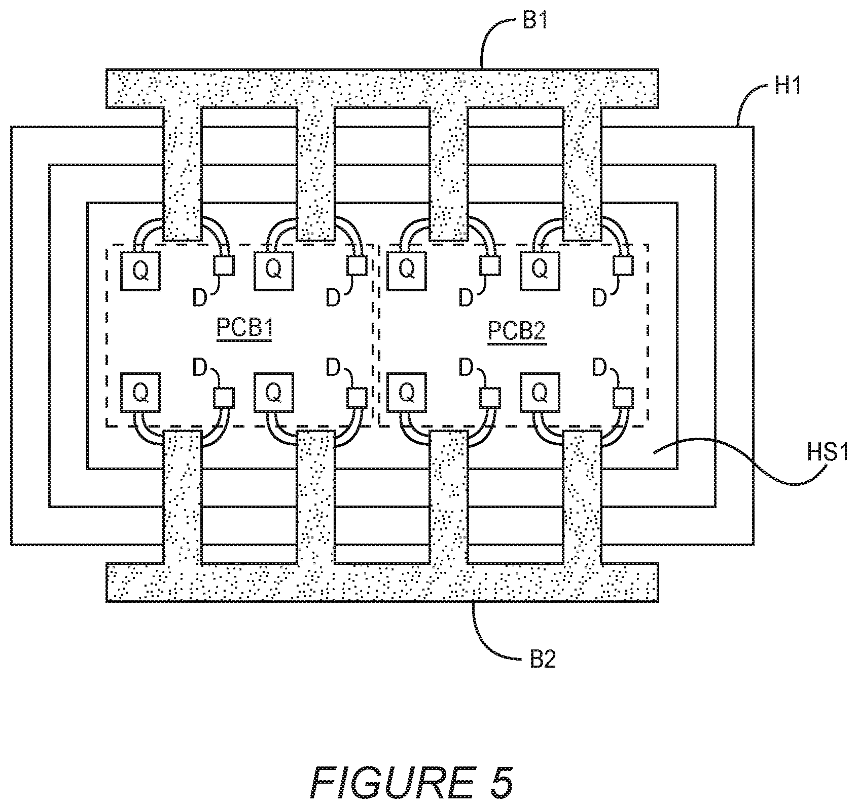
FIG. 5 is a top plan view of a power module according to one embodiment.
FIG. 6 is an isometric view of the power module of FIG. 5.
FIG. 7 is a circuit diagram of a metal-oxide-semiconductor field effect transistor (MOSFET) device.
FIG. 8 is a graph illustrating hypothetical on-state current-voltage characteristics for a MOSFET device.
FIG. 9 is a graph illustrating the effect of source resistance on gate voltage.
FIG. 10 is a partial cross sectional illustration of a cell of a conventional power MOSFET device.
FIGS. 11 and 12 are plan views illustrating layouts of conventional power MOSFET devices.
FIGS. 13 and 14 are plan views illustrating layouts of power MOSFET devices according to some embodiments.
FIGS. 15 and 16 are partial cross sectional illustrations of a cell of a power MOSFET device according to some embodiments.
FIG. 17 is a graph showing on-state current-voltage characteristics for a MOSFET device according to some embodiments.
FIG. 18 is a cross sectional illustration of a cell of a power MOSFET device according to some embodiments.
FIG. 19 is a cross sectional illustration of a cell of an insulated gate bipolar transistor device according to some embodiments.
FIG. 20 is a cross sectional illustration of a cell of a p-type insulated gate bipolar transistor device according to some embodiments.
FIG. 21 is a graph showing current-voltage characteristics of the P-IGBT device of FIG. 20.
FIG. 22A is a graph showing voltage blocking characteristics of the p-IGBT of FIG. 20.
FIG. 22B is a graph showing pulsed on-state current-voltage characteristics of the P-IGBT of FIG. 20.
FIG. 22C is a graph showing further on-state current-voltage characteristics of the P-IGBTs of FIG. 20 for temperatures ranging from room temperature to 300.degree. C.
FIG. 22D is a graph showing on-state current-voltage characteristics of the P-IGBTs of FIG. 22 as a function of temperature.
DETAILED DESCRIPTION OF EMBODIMENTS OF THE DISCLOSURE
Embodiments of the present disclosure now will be described more fully hereinafter with reference to the accompanying drawings, in which embodiments of the disclosure are shown. This disclosure may, however, be embodied in many different forms and should not be construed as limited to the embodiments set forth herein. Rather, these embodiments are provided so that this disclosure will be thorough and complete, and will fully convey the scope of the disclosure to those skilled in the art. Like numbers refer to like elements throughout.
It will be understood that, although the terms first, second, etc. may be used herein to describe various elements, these elements should not be limited by these terms. These terms are only used to distinguish one element from another. For example, a first element could be termed a second element, and, similarly, a second element could be termed a first element, without departing from the scope of the present disclosure. As used herein, the term "and/or" includes any and all combinations of one or more of the associated listed items.
The terminology used herein is for the purpose of describing particular embodiments only and is not intended to be limiting of the disclosure. As used herein, the singular forms "a", "an" and "the" are intended to include the plural forms as well, unless the context clearly indicates otherwise. It will be further understood that the terms "comprises" "comprising," "includes" and/or "including" when used herein, specify the presence of stated features, integers, steps, operations, elements, and/or components, but do not preclude the presence or addition of one or more other features, integers, steps, operations, elements, components, and/or groups thereof.
Unless otherwise defined, all terms (including technical and scientific terms) used herein have the same meaning as commonly understood by one of ordinary skill in the art to which this disclosure belongs. It will be further understood that terms used herein should be interpreted as having a meaning that is consistent with their meaning in the context of this specification and the relevant art and will not be interpreted in an idealized or overly formal sense unless expressly so defined herein.
It will be understood that when an element such as a layer, region or substrate is referred to as being "on" or extending "onto" another element, it can be directly on or extend directly onto the other element or intervening elements may also be present. In contrast, when an element is referred to as being "directly on" or extending "directly onto" another element, there are no intervening elements present. It will also be understood that when an element is referred to as being "connected" or "coupled" to another element, it can be directly connected or coupled to the other element or intervening elements may be present. In contrast, when an element is referred to as being "directly connected" or "directly coupled" to another element, there are no intervening elements present.
Relative terms such as "below" or "above" or "upper" or "lower" or "horizontal" or "lateral" or "vertical" may be used herein to describe a relationship of one element, layer or region to another element, layer or region as illustrated in the figures. It will be understood that these terms are intended to encompass different orientations of the device in addition to the orientation depicted in the figures.
Embodiments of the disclosure are described herein with reference to cross-section illustrations that are schematic illustrations of idealized embodiments (and intermediate structures) of the disclosure. The thickness of layers and regions in the drawings may be exaggerated for clarity. Additionally, variations from the shapes of the illustrations as a result, for example, of manufacturing techniques and/or tolerances, are to be expected. Thus, embodiments of the disclosure should not be construed as limited to the particular shapes of regions illustrated herein but are to include deviations in shapes that result, for example, from manufacturing. For example, an implanted region illustrated as a rectangle will, typically, have rounded or curved features and/or a gradient of implant concentration at its edges rather than a discrete change from implanted to non-implanted region. Likewise, a buried region formed by implantation may result in some implantation in the region between the buried region and the surface through which the implantation takes place. Thus, the regions illustrated in the figures are schematic in nature and their shapes are not intended to illustrate the actual shape of a region of a device and are not intended to limit the scope of the disclosure.
Some embodiments of the disclosure are described with reference to semiconductor layers and/or regions which are characterized as having a conductivity type such as n-type or p-type, which refers to the majority carrier concentration in the layer and/or region. Thus, n-type material has a majority equilibrium concentration of negatively charged electrons, while p-type material has a majority equilibrium concentration of positively charged holes. Some material may be designated with a "+" or "-" (as in n+, n-, p+, p-, n++, n--, p++, p--, or the like), to indicate a relatively larger ("+") or smaller ("-") concentration of majority carriers compared to another layer or region. However, such notation does not imply the existence of a particular concentration of majority or minority carriers in a layer or region.
An exemplary system that employs a power module is illustrated in FIG. 1. As depicted, the power module can include four switch modules SM1-SM4, which are controlled by a control CS1 to deliver power from a power supply PS1 to a load in a controlled manner. The switch modules SM1 and SM2 form a first half of an H-bridge, while switch modules SM3 and SM4 form a second half of the H-bridge. As noted, power modules are often used to drive an inductive load, such as that provided by a direct current (DC) motor M1. The details of the switch modules SM1-SM4 are described in further detail below.
For now, assume the switch modules SM1-SM4 can include at least one transistor in parallel with an internal or external diode that is connected in anti-parallel with the transistor. The transistors are illustrated as metal oxide field effect transistors (MOSFETs), and the diodes are illustrated as Schottky diodes for purposes of description. The MOSFETs may be replaced with other types of transistors, such as bipolar transistors, including insulated gate bipolar transistors (IGBTs), and various kinds of field effect transistors (FETs), such as junction field effect transistors (JFETs), and high electron mobility transistors (HEMTs). Similarly, the Schottky diodes may be replaced with traditional p-n diodes.
As illustrated, switch module SM1 may include either an n-channel or p-channel MOSFET Q1 that has a Schottky diode D1 connected in anti-parallel across the drain and source terminals of the MOSFET Q1. Switch modules SM2-SM4 are similarly configured. Switch module SM2 includes an n-channel MOSFET Q2 that has a Schottky diode D2 connected in anti-parallel across the drain and source terminals of the MOSFET Q2. Switch module SM3 may include either an n-channel or p-channel MOSFET Q3 that has a Schottky diode D3 connected in anti-parallel across the drain and source terminals of the MOSFET Q3. Switch module SM4 includes an n-channel MOSFET Q4 that has a Schottky diode D4 connected in anti-parallel across the drain and source terminals of the MOSFET Q4.
The switch modules SM1 and SM3 are considered on the "high" side, and the switch modules SM2 and SM4 are considered on the "low" side of the power module. The drains of MOSFETs Q1 and Q3 and the cathodes of diodes D1 and D3 are coupled together and to the power supply PS1. The source of MOSFET Q1, the anode of diode D1, the drain of MOSFET Q2, and the cathode of diode D2 are coupled together and to a first terminal of the motor M1. The source of MOSFET Q3, the anode of diode D3, the drain of MOSFET Q4, and the cathode of diode D4 are coupled together and to a second terminal of the motor M1. Finally, the sources of MOSFETs Q2 and Q4 and the anodes of diodes D2 and D4 are coupled to ground. The gates of MOSFETs Q1-Q4 are respectively driven by control signals S1-S4, which are provided by the control system CS1. Assume the motor M1 may be driven in both forward and reverse directions.
For forward operation, assume control signals S1-S4 are configured to turn on MOSFETs Q2 and Q3 and turn off MOSFETs Q1 and Q4, which corresponds to driving the motor M1 in a forward direction. As illustrated in FIG. 2, a forward current i.sub.f flows from the power supply PS1 through MOSFET Q3, the motor M1, and the MOSFET Q2 to ground. If MOSFETs Q2 and Q3 stay on, the maximum forward current i.sub.f is provided and the motor M1 will turn in the forward direction at a maximum speed, with maximum torque, or a combination thereof.
To control the speed or torque, one or both of the MOSFETs Q2 and Q3 may be switched off and on at a duty cycle that corresponds to the speed or torque desired from the motor M1. As a result, the voltage supplied to the motor M1 is pulse width modulated, wherein the on-to-off switching ratio of the MOSFETs Q2 and Q3 dictates the average voltage presented to the motor M1. The inductive nature of the motor M1 tries to keep the forward current i.sub.f constant, and as a result, averages the voltage presented to the motor M1 to a level corresponding to the on-to-off switching ratio of the MOSFETs Q2 and Q3. The average voltage presented to the motor M1 dictates the forward current i.sub.f that is passed through the motor M1, and thus, controls the actual speed or torque of the motor M1.
For reverse operation, assume control signals S1-S4 are configured to turn on MOSFETs Q1 and Q4 and turn off MOSFETs Q2 and Q3. As illustrated in FIG. 3, a reverse current i.sub.r flows from the power supply PS1 through MOSFET Q1, the motor M1, and the MOSFET Q4 to ground. If MOSFETs Q1 and Q4 stay on, the maximum reverse current i.sub.r is provided and the motor M1 will turn in the reverse direction at a maximum speed, with maximum torque, or a combination thereof. Notably, the term "reverse" when used as an adjective in the term "reverse current i.sub.r," merely refers to the direction of operation for the motor M1. The arrows provided in FIGS. 2 and 3, respectively, indicate the direction of current flow for both the forward current i.sub.f and the reverse current i.sub.r.
As described above, the various MOSFETs Q1-Q4 may be turned on and off at a relatively high frequency to provide pulse width modulated voltage to the motor M1 for either forward or reverse operation as well as to switch from forward operation to reverse operation. When a pair of MOSFETs, such as MOSFETs Q2 and Q3 transition from an on-state to an off-state during forward operation, the forward current i.sub.f continues to flow through the motor M1 after the MOSFETs Q2 and Q3 are turned off, due to the electromagnetic field that is present in the inductive windings of the motor M1. At this point, all of the MOSFETs Q1-Q4 are off, yet the forward current i.sub.f remains flowing through the motor M1. Since the forward current i.sub.f cannot flow through any of the MOSFETS Q1-Q4 to a lower potential node, one or more of the Schottky diodes D1 though D4 may become forward biased and provide a path for the forward current i.sub.f to flow to either ground or the power supply PS1.
To increase the power handling of a switch module SM1-SM4, each of the MOSFETs Q1-Q4 may represent an array of effectively parallel transistors. Similarly, each of the Schottky diodes D1-D4 may represent an array of effectively parallel diodes. This concept is represented in FIG. 4 where an exemplary embodiment of switch module SM1 is illustrated. The other switch modules SM2-SM3 may be similarly configured.
As illustrated, switch module SM1 includes an array of MOSFETs Q1.sub.1-Q1.sub.N, which are effectively coupled in parallel, such that the drains are all coupled together and to the power supply PS1; the sources are all coupled together and to the motor M1 and switch module SM2; and the gates are coupled together and to the control system C1 (control signal S1). The Schottky diodes D1.sub.1-D1.sub.N are coupled in anti-parallel across the drain and sources of the MOSFETs Q1.sub.1-Q1.sub.N. The number (N) of MOSFETs Q1.sub.1-Q1.sub.N and Schottky diodes D1.sub.1-D1.sub.N may range from two to more than 100, depending on the capability of each individual device and the application. Notably, there may be two or more Schottky diodes D1 for each MOSFET Q1, even though there is only a one-to-one relationship in the illustration.
FIGS. 5 and 6 show top and perspective views of an exemplary power module. With reference to FIG. 5, rectangular housing H1 is provided with an interior chamber that holds one or more printed circuit boards PCB1 and PCB2. For clarity, the printed circuit boards PCB1 and PCB2 are not shown in FIG. 6. Each printed circuit board PCB1 and PCB2 is shown as having multiple transistors Q and diodes D that represent the primary components of the switch modules SM1-SM4. For example, the high and low side of the first half-H bridge formed by switch modules SM1 and SM2 are provided on printed circuit board PCB1, while the high and low side of the second half-H bridge formed by switch modules SM3 and SM4 are provided on printed circuit board PCB2. Together, the first and second half-H bridges form the above-described full-H bridge.
The necessary interconnects between the components on the printed circuit boards PCB1 and PCB2 are provided by metal traces (not shown) on the printed circuit boards PCB1 and PCB2. Bond wires may be used to make connections between the printed circuit boards PCB1 and PCB2 and one more connectors or buses B1 and B2. For example, bus B1 may be used to connect switch modules SM2 and SM4 to ground, and bus B2 may be used to connect switch modules SM1 and SM3 to the power supply PS1. These or other connectors may be used for the control signals S1-S4. The printed circuit boards PCB1 and PCB2 may be mounted to a mounting structure that is affixed to the housing H1. As illustrated, the mounting structure is a planar heat sink HS1 that also functions to dissipate heat generated by the switch modules SM1-SM4.
Again, the H-bridge configuration of the power module is just one of many available designs for power modules, especially those used to drive inductive loads. Alternatives to the H-bridge configuration for the power module include a half-H bridge and like known power switching or control circuits.
Regardless of the type of configuration of the power module, one metric for measuring the power handling capabilities of the device is current density of one of the switch modules SM1-SM4. This switch module current density is defined as the ratio of the maximum average current that a single switch module SM1-SM4 can handle to the interior area of the housing H1 that is allocated to the single switch module SM1-SM4. For the illustrated example, there are four switch modules SM1-SM4 of equal size. As such, the interior area of the housing H1 that is allocated to a single switch module SM1-SM4 is one-fourth (1/4) the total interior area of the housing H1.
For example, assume the interior area of the housing H1 is 100 cm.sup.2, and the maximum average current handling of one of the switch modules SM1-SM4 is 250 amperes. As such, the interior area of the housing H1 that is allocated to a single switch module SM1-SM4 is one-fourth of 100 cm.sup.2, or 25 cm.sup.2. The switch module current density is calculated by dividing the maximum average current handling of 250 amperes by the interior area of the housing H1 that is allocated to the single switch module SM1-SM4, which yields 10 amperes/cm.sup.2.
The interior area of the housing H1 is defined as the maximum (two-dimensional) cross-sectional area of the interior of the housing H1 wherein the plane of measurement is along the plane in which one or more printed circuit boards PCB1 and PCB2 or one or more semiconductor die that provide the switch modules SM1-SM4 reside. For the illustrated example in FIG. 5, the interior area is defined by the perimeter of the inside wall of the housing H1. Notably, since the housing H1 may have various shapes and configurations in addition to the rectangular configuration shown in FIGS. 5 and 6, the interior areas need not be rectangular and the perimeter of the interior areas will follow the interior sidewalls of the housing H1. In one embodiment, the switch module current density is about 10 amperes/cm.sup.2 or greater. In another embodiment, the switch module current density is about 12 amperes/cm.sup.2 or greater. In another embodiment, the switch module current density is about 15 amperes/cm.sup.2 or greater.
The following description outlines several transistor configurations that can be used in the power module as MOSFETs Q1.sub.N-Q4.sub.N or alternatives thereto. Other transistor configurations may be employed. Some embodiments of the disclosure provide silicon carbide (SiC) insulated gate devices that are suitable for high power and/or high temperature applications.
FIG. 7 is a circuit diagram of a metal oxide semiconductor field effect transistor (MOSFET) device 10. As shown therein, a MOSFET device generally includes three terminals, namely, a drain terminal (D), a source terminal (S) and a gate terminal (G). The gate-to-source voltage of the device is denoted V.sub.GS, while the drain-to-source voltage of the device is denoted V.sub.DS. The device has a built in source resistance R.sub.S and a built-in drain resistance R.sub.D based on the physical characteristics of the device. The voltage over the built-in source resistance R.sub.S is denoted V.sub.Rs.
In a MOSFET device, current passing through a channel of the device from the drain to the source is regulated by applying a voltage to the gate. The gate is insulated from the channel by a gate insulator, such as silicon dioxide. As the voltage on the gate terminal is increased, current passing through the device may increase.
FIG. 8 is a graph illustrating hypothetical curve 102 and actual 104 on-state current-voltage characteristics for a MOSFET device for a given gate-to-source voltage (V.sub.GS). As shown in FIG. 8, for a given gate voltage, the current through the device (I.sub.D) increases as the voltage between the drain and source (V.sub.DS) increases, up to a saturation point. In actual devices, the actual saturation current of a transistor is typically less than the ideal saturation current. Part of the reason for this relates to the source resistance of the device.
In particular, as the drain current I.sub.D passing through the device increases, the amount of voltage dropped over the source resistance R.sub.S increases in direct proportion. FIG. 9 is a graph illustrating the effect of source resistance on gate voltage. In FIG. 9, the voltage from the gate terminal to the source terminal is denoted V.sub.GS. A portion of the gate voltage V.sub.GS applied to the device across the gate and source terminals is dropped over the internal source resistance R.sub.S of the device. That portion of the gate voltage is denoted V.sub.Rs in FIG. 9. The remainder of the gate-to-source voltage appears as a voltage across the gate insulator, denoted V.sub.GS,int in FIG. 9. Thus, V.sub.GS is equal to the sum of V.sub.Rs and V.sub.GS,int.
As shown in FIG. 9, the gate-to-source voltage may remain constant as the drain current increases. However, the portion of the gate voltage V.sub.GS that is dropped over the internal source resistance of the device, V.sub.Rs, increases as the drain current I.sub.D increases, while the portion of the gate-to-source voltage that appears as a voltage across the gate insulator, V.sub.GS,int, decreases as the drain current I.sub.D increases.
Thus, as the drain current increases the portion of the gate voltage that is being used to maintain the channel decreases, which may cause the device to go into saturation at a lower level of drain-to-source voltage. Accordingly, a high source resistance can adversely affect the operation of a MOSFET or other insulated gate controlled device.
A unit cell of a MOSFET structure according to some embodiments is shown in FIG. 10. The device of FIG. 10 includes an n- drift epitaxial layer 14 on an n-type, 8.degree. off-axis 4H-SiC substrate 12. The n- drift layer 14 may have a thickness of about 100 .mu.m to about 120 .mu.m, and may be doped with n-type dopants at a doping concentration of about 2.times.10.sup.14 cm.sup.-3 to about 6.times.10.sup.14 cm.sup.-3 for a blocking capability of about 10 kV. Other doping concentrations/voltage blocking ranges are also possible. For a 1200V MOSFET device, the substrate may be 4.degree. off-axis 4H-SiC and the drift layer may have a thickness of about 10 .mu.m and may be doped with n-type dopants at a doping concentration of about 6.times.10.sup.15 cm.sup.-3.
The structure further includes a p+ well region 18 and an n+ source region 20 that may be formed by selective implantation of, for example, aluminum and nitrogen, respectively. The junction depth of the p+ well region 18 may be about 0.5 .mu.m, although other depths are possible. The structure further includes a p+ contact region 22 that extends from a surface of the drift layer 14 into the p+ well region 18. A junction termination (not shown) may be provided around the device periphery.
All of the implanted dopants may be activated by annealing the structure at a temperature of about 1600.degree. C. with a silicon over pressure and/or covered by an encapsulation layer such as a graphite film. A high temperature anneal may damage the surface of the silicon carbide epitaxy without these conditions. The silicon overpressure may be provided by the presence of silane, or the close proximity of silicon carbide coated objects that provide a certain amount of silicon overpressure. Alternatively or in combination with silicon overpressure, a graphite coating may be formed on the surface of the device. Prior to annealing the device to activate the implanted ions, a graphite coating may be applied to the top/front side of the structure in order to protect the surface of the structure during the anneal. The graphite coating may be applied by a conventional resist coating method and may have a thickness of about 1 .mu.m. The graphite coating may be heated to form a crystalline coating on the drift layer 14. The implanted ions may be activated by a thermal anneal that may be performed, for example, in an inert gas at a temperature of about 1600.degree. C. or greater. In particular the thermal anneal may be performed at a temperature of about 1600.degree. C. in argon for 5 minutes. The graphite coating may help to protect the surface of the drift layer 14 during the high temperature anneal.
The graphite coating may then be removed, for example, by ashing and thermal oxidation.
After implant annealing, a field oxide of silicon dioxide (not shown) having a thickness of about 1 .mu.m may be deposited and patterned to expose the active region of the device.
A gate oxide layer 36 may be formed by a gate oxidation process, with a final gate oxide thickness of 400-600 .ANG..
In particular, the gate oxide may be grown by a dry-wet oxidation process that includes a growth of bulk oxide in dry O.sub.2 followed by an anneal of the bulk oxide in wet O.sub.2 as described, for example, in U.S. Pat. No. 5,972,801, the disclosure of which is incorporated herein by reference in its entirety. As used herein, anneal of oxide in wet O.sub.2 refers to anneal of an oxide in an ambient containing both O.sub.2 and vaporized H.sub.2O. An anneal may be performed in between the dry oxide growth and the wet oxide growth. The dry O.sub.2 oxide growth may be performed, for example, in a quartz tube at a temperature of up to about 1200.degree. C. in dry O.sub.2 for a time of at least about 2.5 hours. Dry oxide growth is performed to grow the bulk oxide layer to a desired thickness. The temperature of the dry oxide growth may affect the oxide growth rate. For example, higher process temperatures may produce higher oxide growth rates. The maximum growth temperature may be dependent on the system used.
In some embodiments, the dry O.sub.2 oxide growth may be performed at a temperature of about 1175.degree. C. in dry O.sub.2 for about 3.5 hours. The resulting oxide layer may be annealed at a temperature of up to about 1200.degree. C. in an inert atmosphere. In particular, the resulting oxide layer may be annealed at a temperature of about 1175.degree. C. in Ar for about 1 hour. The wet O.sub.2 oxide anneal may be performed at a temperature of about 950.degree. C. or less for a time of at least about 1 hour. The temperature of the wet O.sub.2 anneal may be limited to discourage further thermal oxide growth at the SiC/SiO.sub.2 interface, which may introduce additional interface states. In particular, the wet O.sub.2 anneal may be performed in wet O.sub.2 at a temperature of about 950.degree. C. for about 3 hours. The resulting gate oxide layer may have a thickness of about 500 .ANG..
In some embodiments, the dry O.sub.2 oxide growth may be performed at a temperature of about 1175.degree. C. in dry O.sub.2 for about 4 hours. The resulting oxide layer may be annealed at a temperature of up to about 1175.degree. C. in an inert atmosphere. In particular, the resulting oxide layer may be annealed at a temperature of about 1175.degree. C. in Ar for about a time duration ranging from 30 min to 2 hours. Then the oxide layer receives an anneal in NO ambient at a temperature ranging from 1175.degree. C. to 1300C, for a duration ranging from 30 minutes to 3 hours. The resulting gate oxide layer may have a thickness of about 500 .ANG..
After formation of the gate oxide 36, a polysilicon gate 32 may be deposited and doped, for example, with boron followed by a metallization process to reduce the gate resistance. Al/Ni contacts may be deposited as the p-type ohmic source contact metal 34, and Ni as the n-type drain contact metal 26. All contacts may be sintered in a Rapid Thermal Annealer (RTA), and thick Ti/Au layers may be used for pad metals
Referring to FIG. 10, the source resistance of a MOSFET device has two primary components, namely, the contact resistance R.sub.C between the source ohmic contact 34 and the source region 20, and the sheet resistance R.sub.sheet in the source region 20 between the source ohmic contact 34 and the channel. Thus, R.sub.S=R.sub.C+R.sub.sheet. In a conventional silicon-based MOSFET device, the sheet resistance R.sub.sheet is the dominant factor in determining the source resistance, because it is possible to form very low resistivity ohmic contacts to silicon and other narrow-bandgap semiconductors. However, in wide bandgap semiconductors (i.e., semiconductors having a bandgap greater than about 2.0 V), including compound semiconductor materials, such as silicon carbide and gallium nitride, diamond, and ZnO, the contact resistance R.sub.C may be the dominant contributor to the source resistance. In particular, it is difficult to form very low resistivity ohmic contacts to silicon carbide and other wide bandgap materials because of the high energy barrier associated with such materials.
FIGS. 11 and 12 are plan views illustrating layouts of conventional power MOSFET devices. In a conventional power MOSFET device, the layout is designed to reduce or minimize sheet resistance under the assumption that contact resistance is less important than sheet resistance. Thus, referring to FIG. 11, a conventional power MOSFET device typically includes a p-well 18 formed in a drift layer 14, an n+ source region 20 in the p-well 18, and a p+ contact region 22 in the n+ source region 20. Referring to FIG. 12, a source contact 34 is formed on the n+ source region 20 and the p+ contact region 22. A gate 32 is formed over the p-well 18 and overlaps the periphery of the n+ source region 20 and adjacent portions of the drift layer 14. Current flow from the drain to the source is indicated by the arrows 42 in FIG. 11.
As noted above, in a wide bandgap semiconductor material system, the source resistance may be more affected by the contact resistance of the source ohmic contact than by the sheet resistance of the source layer. Accordingly, to decrease the source resistance of a wide bandgap power semiconductor device, it may be desirable to decrease the contact resistance of the source ohmic contact. In general, contact resistance can be decreased by increasing the minimum dimension of the contact, which is the smallest dimension of the contact in any direction. However, simply increasing the minimum dimension of the source ohmic contact of an electronic device can undesirably increase the cell to cell spacing, or pitch, of the device. The pitch of a MOSFET device may be proportional to the width of the p-well region of the device. Increasing the pitch of the device reduces the density of the devices that can be formed on a single substrate, reducing the devices yielded and increasing manufacturing costs.
According to some embodiments, an insulated gate device layout is provided that increases the minimum dimension of the source ohmic contact without increasing the pitch of the device and/or the width of the p-well region of the device. A device layout according to some embodiments may increase the sheet resistance of the device. Such an effect may be highly undesirable in a device based on a narrow bandgap semiconductor material. However, since sheet resistance is not the dominant factor in determining source resistance of a wide bandgap device, such a tradeoff may be acceptable for wide bandgap devices. In devices according to some embodiments, a ratio of the source sheet resistance to the source contact resistance may be greater than 0.75 (i.e. R.sub.sheet/R.sub.C>0.75). In some embodiments, the device may have a source contact resistance that is less than the source sheet resistance. That is, in some embodiments, the ratio of the source sheet resistance to the source contact resistance may be greater than 1 (i.e. R.sub.sheet/R.sub.C>1), and in further embodiments, the ratio of the source sheet resistance to the source contact resistance may be greater than 5.
FIGS. 13 and 14 are plan views illustrating layouts of MOSFET device cells according to some embodiments, and FIGS. 15 and 16 are partial cross sectional illustrations of a cell of a MOSFET device according to some embodiments. In particular, FIG. 15 is a cross section taken along line A-A' of FIG. 13, while FIG. 16 is a cross section taken along line B-B' of FIG. 14.
The device shown in FIGS. 13-16 includes an n- drift epitaxial layer 114 on an n-type, 8.degree. off-axis 4H-SiC substrate 112. The n- drift layer 114 may have a thickness of about 100 .mu.m to about 120 .mu.m, and may be doped with n-type dopants at a doping concentration of about 2.times.10.sup.14 cm.sup.-3 to about 6.times.10.sup.14 cm.sup.-3 for a blocking capability of about 10 kV. For a 1200V MOSFET device, the substrate may be 4.degree. off-axis 4H-SiC and the drift layer may have a thickness of about 10 .mu.m and may be doped with n-type dopants at a doping concentration of about 6.times.10.sup.15 cm.sup.-3.
The structure further includes a p+ well region 118 and an n+ source region 120 that may be formed by selective implantation of, for example, aluminum and nitrogen, respectively. The junction depth of the p+ well region 118 may be about 0.5 .mu.m. The structure further includes a plurality of p+ contact regions 122 that extend from a surface of the drift layer 114 into the p+ well region 118. A junction termination (not shown) may be provided around the device periphery.
Referring to FIG. 13, the n+ source region 120 includes a pair of lateral source regions 120A that are parallel to opposing channel regions 125 in the p-well 118. A plurality of source contact regions 120B extend between the lateral source regions 120A, and the plurality of p+ contact regions 122 are provided between the source contact regions 120B.
Referring to FIG. 14, gate contacts 132 are formed over the channel regions 125 and overlap the lateral source regions 120A. A source ohmic contact 134 is formed across the source contact regions 120B and the p+ contact regions 122. The source ohmic contact 134 overlaps the source contact regions 120B in a source contact region 136. The source ohmic contact 134 overlaps the p+ contact regions 122 in a body contact region 138.
The portion of the source contact regions 120B contacted by the source ohmic contact 134 may have a minimum dimension that is larger than the minimum dimension that can be obtained for a conventional layout such as the layout shown in FIGS. 11 and 12 for a similar pitch/p-well size. Accordingly, the source contact resistance may be reduced without substantially increasing the device pitch/p-well size. The "minimum dimension" of a feature refers to the smallest width of the feature in any cross section of the feature. For example, the minimum dimension p1 of the body contact region 138, the minimum dimension n1 of the n-type contact region 136, and the minimum dimension w1 of the p-well region 118 are shown in FIG. 14.
In a device having a layout as shown in FIGS. 13 and 14, current flow to the source contact flows through the source contact regions 120B, as indicated by the arrows 142 in FIG. 13. The source contact regions 120B may have an increased sheet resistance compared to the source region of a device having a conventional layout as shown in FIGS. 11 and 12. However, the increase in sheet resistance may be more than compensated by the decrease in contact resistance, thus providing an overall decrease in the source resistance of the device.
FIG. 17 is a graph of on-state current-voltage characteristics for a 7 mm.times.8 mm 1200 V silicon carbide MOSFET device according to some embodiments. In the device characteristics illustrated in FIG. 17, a drain current (I.sub.D) of 377 A was measured at a forward voltage drain-to-source voltage (V.sub.DS) of 3.8 V. The current density, normalized to the active area, was over 750 A/cm.sup.2.
The on-resistance of a MOSFET device is affected by the drain resistance, the channel resistance and the source resistance of the device. Accordingly, reducing the source resistance of the device also reduces the on-resistance of the device.
A wide bandgap MOSFET device having a layout according to some embodiments may be capable of substantially increased saturation current due to the lower on-resistance of the device and the fact that increased current levels have less of a de-biasing effect on the gate. That is, because of the lower source resistance, less voltage will be developed over the source resistance as the drain current increases. Thus, more of the gate-to-source voltage is applied to the channel of the device.
FIG. 18 is an idealized cross section of a device having a layout in accordance with some embodiments. In particular, FIG. 18 illustrates some dimensions of a device having a layout in accordance with some embodiments. For example, as shown in FIG. 18, the minimum dimension of the implanted cell area (i.e. the p-well 118) is denoted as width w1 in FIG. 18. It will be appreciated, however, that the minimum dimension of the p-well 118 may occur in a dimension that is different from the plane of the device illustrated in FIG. 18. For example, the minimum dimension of the p-well 118 may occur in a dimension that is perpendicular to the plane of the device illustrated in FIG. 18.
The minimum dimension of the n-type contact area is denoted as width n1 in FIG. 18, while the minimum dimension of the p-type contact area is denoted as width p1 in FIG. 18. The n-type contact area may be defined as the area of overlap between the source ohmic contact 132 and the n+ source region 120, while the p-type contact area may be defined as the area of overlap between the source ohmic contact 132 and the p+ contact regions 122.
An insulated gate bipolar transistor (IGBT) device 200 according to some embodiments is illustrated in FIG. 19. As shown therein, the IGBT device includes an n- drift epitaxial layer 214 on a p-type epitaxial layer 212. The p-type epitaxial layer 212 is formed on a heavily doped p-type, 8.degree. off-axis 4H-SiC substrate or layer 210. The n- drift layer 214 may have a thickness of about 100 .mu.m to about 120 .mu.m, and may be doped with p-type dopants at a doping concentration of about 2.times.10.sup.14 cm.sup.-3 to about 6.times.10.sup.14 cm.sup.-3 for a blocking capability of about 10 kV.
The IGBT structure 200 further includes a p+ well region 218 and an n+ source/emitter region 220 that may be formed by selective implantation of, for example, aluminum and nitrogen, respectively. The junction depth of the p+ well region 218 may be about 0.5 .mu.m. The structure 200 further includes a plurality of p+ body contact regions 222 that extend from a surface of the drift layer 214 into the p+ well region 218. The conductivity types may be reversed in some embodiments.
A gate contact 232 is on a gate insulator 236, a source/emitter contact 234 is on the source contact regions 220 and the body contact regions 222. A collector contact 226 contacts the substrate 210.
According to some embodiments, a transistor device may have a ratio of n1 to w1 that is greater than 0.2. In further embodiments, a transistor device may have a ratio of n1 to w1 that is greater than about 0.3. In further embodiments, a transistor device may have a ratio of n1 to w1 that is in the range of about 0.2 to 1. In further embodiments, a transistor device may have a ratio of n1 to w1 that is in the range of about 0.3 to 1. In further embodiments, transistor device may have a ratio of n1 to w1 that is greater than 0.5. For example, the minimum dimension n1 of the n-type contact area of a device having a layout according to some embodiments may be about 2 .mu.m for a device having a minimum dimension of the implanted cell area of 6 .mu.m.
According to some embodiments, a transistor device may have a ratio of p1 to w1 that is greater than 0.2. In further embodiments, a transistor device may have a ratio of p1 to w1 that is greater than about 0.3. In further embodiments, a transistor device may have a ratio of p1 to w1 that is greater than about 0.5. In further embodiments, a transistor device may have a ratio of p1 to w1 that is in the range of about 0.2 to 0.5. In further embodiments, a transistor device may have a ratio of p1 to w1 that is in the range of about 0.2 to 1.
Some embodiments provide transistor devices having increased current densities. Current density is defined as the total current divided by the area of the chip. For example, a wide bandgap transistor device according to some embodiments may be capable of current densities in excess of 200 A/cm.sup.2 and a blocking voltage of 1000 V or more. A wide bandgap transistor device according to further embodiments may be capable of a current of 100 A or greater at current densities in excess of 200 A/cm.sup.2, a forward voltage drop of less than 5 V and a blocking voltage of 1000 V or more. A wide bandgap transistor device according to still further embodiments may be capable of a current of 100 A or greater at current densities in excess of 300 A/cm.sup.2, a forward voltage drop of less than 5 V and a blocking voltage of 1000 V or more.
A semiconductor device according to some embodiments has a reverse blocking voltage in excess of 1000 volts and a current density greater than 200 amps per square centimeter at a current greater than 100 A.
A semiconductor device according to further embodiments has a reverse blocking voltage of 1000 volts or more and a forward current capability greater than 100 A at a forward voltage of 5 volts or less.
A metal-oxide semiconductor field effect transistor device according to some embodiments has a reverse blocking voltage of 1200 volts or more and a forward current capability greater than 100 A.
A metal-oxide semiconductor field effect transistor device according to some embodiments has a reverse blocking voltage of 1000 volts or more and a differential on-resistance less than 8 mOhms-cm.sup.2.
A semiconductor device having a blocking voltage less than 1000 V and configured to pass forward current at a current density greater than 200 amps per square centimeter at a forward voltage drop of 5 V or less.
Some embodiments may enable wide bandgap transistor devices to achieve drain currents of 100 Amps or higher at a drain to source voltage that is less than 4 Volts in a device having a cell pitch of less than 20 .mu.m. Some embodiments may enable wide bandgap transistor devices to achieve drain currents of 100 Amps or higher at a drain to source voltage that is less than 4 Volts in a device having a cell pitch of less than 10 .mu.m. Some embodiments may enable wide bandgap transistor devices to achieve drain currents of 80 Amps or higher at a drain to source voltage that is less than 5 Volts in a device having a cell pitch of less than 10 .mu.m.
An IGBT device according to some embodiments with a voltage blocking capability of 10 kV or greater may have a differential specific on-resistance of less than 14 mOhm-cm.sup.2 with a forward voltage drop of 5.2 V or less at a current density of 100 A/cm.sup.2.
A p-type insulated gate bipolar transistor (p-IGBT) device 300 according to some embodiments is illustrated in FIG. 20. As shown therein, the IGBT device includes a p- drift epitaxial layer 314 on a p-type field stop buffer layer 311 formed on an n-type, 8.degree. off-axis 4H-SiC substrate 310. The p- drift layer 314 may have a thickness of about 100 .mu.m to about 200 .mu.m, and may be doped with p-type dopants at a doping concentration of about 2.times.10.sup.14 cm.sup.-3 to about 6.times.10.sup.14 cm.sup.-3.
The p-IGBT structure 300 further includes an n+ well region 318 and a p+ source/emitter region 320 that may be formed by selective implantation of, for example, nitrogen and aluminum, respectively. The junction depth of the n+ well region 318 may be about 0.5 .mu.m. The structure 300 further includes a plurality of n+ body contact regions 322 that extend from a surface of the drift layer 314 into the n+well region 318.
A gate contact 332 is on a gate insulator 336, a source/emitter contact 334 is on the source contact regions 320 and the body contact regions 322. A collector contact 326 contacts the substrate 310.
A 4H-SiC p-IGBT as shown in FIG. 20 was fabricated using a 2.times.10.sup.14 cm.sup.-3 doped, 140 .mu.m thick p-type epilayer as the drift layer 314, and a 2 .mu.m thick p-type Field-Stop buffer layer 311, with a doping concentration ranging from 1.times.10.sup.17 cm.sup.-3 to 5.times.10.sup.17 cm.sup.3. A multi-zone JTE (15 zone) edge termination structure (not shown) was formed by nitrogen ion implantation. JTE terminations are described, for example, in U.S. Pat. No. 6,002,159, which is incorporated herein by reference. MOS channels were formed on implanted n-wells 318. A 50 nm thick thermally grown oxide layer was used as the gate insulator 336.
FIG. 21 shows the I.sub.D-V.sub.GS characteristics of the p-IGBT device shown in FIG. 20, with V.sub.DS fixed at -50 mV. The I.sub.D-V.sub.GS characteristics were measured from a test MOSFET with a W/L of 200 .mu.m/200 .mu.m, fabricated on the same wafer. A threshold voltage of -10 V, and a peak MOS channel mobility of 10 cm.sup.2/Vs were extracted from the I.sub.D-V.sub.GS characteristics.
FIG. 22A shows the blocking characteristics (V.sub.GE=0 V) of a 6.7 mm.times.6.7 mm 4H-SiC P-IGBT, with an active area of 0.16 cm.sup.2 at room temperature. The measurement voltage was limited to -15 kV, due to the limitation of probing equipment. The device showed a leakage current of 0.6 .mu.A, which corresponds to a leakage current density of 1.2 .mu.A/cm.sup.2 at a V.sub.CE of -15 kV. This is the highest blocking voltage ever reported in SiC power switches. FIG. 22B shows the pulsed on-state I-V characteristics of the p-IGBT, measured using a Tektronix 371 curve tracer. The device showed an on-state current of -145 A, which represents a current density of 906 A/cm.sup.2, at a V.sub.CE of -22.5 V and a V.sub.GE of -20 V. No evidence of parasitic thyristor latch-up was observed during this measurement. FIG. 22C shows I.sub.C-V.sub.GE characteristics of the 4H-SiC P-IGBTs for temperatures ranging from room temperature to 300.degree. C. V.sub.CE was fixed at -10V for this measurement. The I-V characteristics shifted towards zero at elevated temperature. However, the device maintained normally-off properties throughout the temperature range. FIG. 22D shows the on-state I-V characteristics as a function of temperature. V.sub.GE was fixed at -20 V for this measurement. A monotonic decrease in forward voltage drop with increasing temperature was observed. This is believed due to the increase in minority carrier (electron) diffusion length, caused by increased carrier lifetime at elevated temperatures.
Accordingly, a p-IGBT according to some embodiments may have a reverse blocking voltage that is greater than about 10 kV, and in some cases greater than about 13 kV, and that has a forward current capability greater than 5 Amps.
It will be appreciated that although some embodiments of the disclosure have been described in connection with silicon carbide IGBT and MOSFET devices having n-type drift layers, the present disclosure is not limited thereto, and may be embodied in devices having p-type substrates and/or drift layers. Furthermore, the disclosure may be used in many different types of devices, including but not limited to insulated gate bipolar transistors (IGBTs), MOS controlled thyristors (MCTs), insulated gate commutated thyristors (IGCTs), junction field effect transistors (JFETs), high electron mobility transistors (HEMTs), etc.
In the drawings and specification, there have been disclosed typical embodiments of the disclosure and, although specific terms are employed, they are used in a generic and descriptive sense only and not for purposes of limitation, the scope of the disclosure being set forth in the following claims.
* * * * *
References
D00000
D00001
D00002
D00003
D00004
D00005
D00006
D00007
D00008
D00009
D00010
D00011
D00012

D00013

D00014

XML
uspto.report is an independent third-party trademark research tool that is not affiliated, endorsed, or sponsored by the United States Patent and Trademark Office (USPTO) or any other governmental organization. The information provided by uspto.report is based on publicly available data at the time of writing and is intended for informational purposes only.
While we strive to provide accurate and up-to-date information, we do not guarantee the accuracy, completeness, reliability, or suitability of the information displayed on this site. The use of this site is at your own risk. Any reliance you place on such information is therefore strictly at your own risk.
All official trademark data, including owner information, should be verified by visiting the official USPTO website at www.uspto.gov. This site is not intended to replace professional legal advice and should not be used as a substitute for consulting with a legal professional who is knowledgeable about trademark law.