Image sensor synchronization without input clock and data transmission clock
Blanquart , et al. April 20, 2
U.S. patent number 10,980,406 [Application Number 16/730,737] was granted by the patent office on 2021-04-20 for image sensor synchronization without input clock and data transmission clock. This patent grant is currently assigned to DePuy Synthes Products, Inc.. The grantee listed for this patent is DePuy Synthes Products, Inc.. Invention is credited to Laurent Blanquart, Donald M. Wichern.


View All Diagrams
| United States Patent | 10,980,406 |
| Blanquart , et al. | April 20, 2021 |
Image sensor synchronization without input clock and data transmission clock
Abstract
The disclosure extends to systems and methods for reducing the area of an image sensor by reducing the imaging sensor pad count used for data transmission and clock generation.
| Inventors: | Blanquart; Laurent (Westlake Village, CA), Wichern; Donald M. (Ogden, UT) | ||||||||||
|---|---|---|---|---|---|---|---|---|---|---|---|
| Applicant: |
|
||||||||||
| Assignee: | DePuy Synthes Products, Inc.
(Raynham, MA) |
||||||||||
| Family ID: | 1000005497535 | ||||||||||
| Appl. No.: | 16/730,737 | ||||||||||
| Filed: | December 30, 2019 |
Prior Publication Data
| Document Identifier | Publication Date | |
|---|---|---|
| US 20200138279 A1 | May 7, 2020 | |
Related U.S. Patent Documents
| Application Number | Filing Date | Patent Number | Issue Date | ||
|---|---|---|---|---|---|
| 14214790 | Mar 15, 2014 | 10517469 | |||
| 61790590 | Mar 15, 2013 | ||||
| 61800502 | Mar 15, 2013 | ||||
| Current U.S. Class: | 1/1 |
| Current CPC Class: | H04N 5/3765 (20130101); A61B 1/045 (20130101); A61B 1/0638 (20130101); A61B 1/05 (20130101); H04N 2005/2255 (20130101) |
| Current International Class: | H04N 5/376 (20110101); A61B 1/045 (20060101); A61B 1/06 (20060101); A61B 1/05 (20060101); H04N 5/225 (20060101) |
References Cited [Referenced By]
U.S. Patent Documents
| 3796220 | March 1974 | Bredemeier |
| 3858577 | January 1975 | Bass et al. |
| 4011403 | March 1977 | Epstein et al. |
| 4153356 | May 1979 | Hama |
| 4350150 | September 1982 | Kubota et al. |
| 4363963 | December 1982 | Ando |
| 4429686 | February 1984 | Hosoda |
| 4433675 | February 1984 | Konoshima |
| 4436095 | March 1984 | Kruger |
| 4561430 | December 1985 | Walsh |
| 4572164 | February 1986 | Yoshida et al. |
| 4589404 | May 1986 | Barath et al. |
| 4600940 | July 1986 | Sluyter |
| 4604992 | August 1986 | Sato |
| 4670653 | June 1987 | McConkie et al. |
| 4740837 | April 1988 | Yanagisawa et al. |
| 4741327 | May 1988 | Yabe |
| 4745471 | May 1988 | Takamura et al. |
| 4773396 | September 1988 | Okazaki |
| 4786965 | November 1988 | Yabe |
| 4800424 | January 1989 | Noguchi |
| 4831444 | May 1989 | Kato |
| 4832003 | May 1989 | Yabe |
| 4845555 | July 1989 | Yabe et al. |
| 4853772 | August 1989 | Kikuchi |
| 4866526 | September 1989 | Ams et al. |
| 4888639 | December 1989 | Yabe et al. |
| 4918521 | April 1990 | Yabe et al. |
| 4938205 | July 1990 | Nudelman |
| 4942473 | July 1990 | Zeevi et al. |
| 4953539 | September 1990 | Nakamura et al. |
| 4954878 | September 1990 | Fox et al. |
| 5010038 | April 1991 | Fox et al. |
| 5010876 | April 1991 | Henley et al. |
| 5016975 | May 1991 | Sasaki et al. |
| 5021888 | June 1991 | Kondou et al. |
| 5042915 | August 1991 | Akutsu et al. |
| 5065444 | November 1991 | Garber |
| RE33854 | March 1992 | Adair |
| 5103497 | April 1992 | Hicks |
| 5111804 | May 1992 | Funakoshi |
| 5115309 | May 1992 | Hang |
| 5133035 | July 1992 | Hicks |
| 5168361 | December 1992 | Hackmann |
| 5168863 | December 1992 | Kurtzer |
| 5187572 | February 1993 | Nakamura et al. |
| 5188094 | February 1993 | Adair |
| 5196938 | March 1993 | Blessinger |
| 5200838 | April 1993 | Nudelman et al. |
| 5220198 | June 1993 | Tsuji |
| 5227662 | July 1993 | Ohno et al. |
| 5228430 | July 1993 | Sakamoto |
| 5237403 | August 1993 | Sugimoto et al. |
| 5241170 | August 1993 | Field, Jr. et al. |
| 5277172 | January 1994 | Sugimoto |
| 5289555 | February 1994 | Sanso |
| 5307804 | May 1994 | Bonnet |
| 5313306 | May 1994 | Kuban et al. |
| 5325847 | July 1994 | Matsuno |
| 5339275 | August 1994 | Hyatt |
| 5381784 | January 1995 | Adair |
| 5400267 | March 1995 | Denen et al. |
| 5402768 | April 1995 | Adair |
| 5411020 | May 1995 | Ito |
| 5427087 | June 1995 | Ito et al. |
| 5454366 | October 1995 | Ito et al. |
| 5461425 | October 1995 | Fowler et al. |
| 5471515 | November 1995 | Fossum et al. |
| 5489801 | February 1996 | Blish, II |
| 5494483 | February 1996 | Adair |
| 5522006 | May 1996 | Takeuchi et al. |
| 5523786 | June 1996 | Parulski |
| 5550595 | August 1996 | Hannah |
| 5576781 | November 1996 | Deleeuw |
| 5594282 | January 1997 | Otsuki |
| 5594497 | January 1997 | Ahem et al. |
| 5614763 | March 1997 | Womack |
| 5665959 | September 1997 | Fossum et al. |
| 5721422 | February 1998 | Bird |
| 5734418 | March 1998 | Danna |
| 5748234 | May 1998 | Lippincott |
| 5754313 | May 1998 | Pelchy et al. |
| 5757075 | May 1998 | Kitaoka |
| 5784099 | July 1998 | Lippincott |
| 5787298 | July 1998 | Broedner et al. |
| 5841126 | November 1998 | Fossum et al. |
| 5857963 | January 1999 | Pelchy et al. |
| 5879289 | March 1999 | Yarush et al. |
| 5887049 | March 1999 | Fossum |
| 5896166 | April 1999 | D'Alfonso et al. |
| 5907178 | May 1999 | Baker et al. |
| 5929901 | July 1999 | Adair et al. |
| 5949483 | September 1999 | Fossum et al. |
| 5986693 | November 1999 | Adair et al. |
| 5990506 | November 1999 | Fossum et al. |
| 6005619 | December 1999 | Fossum |
| 6021172 | February 2000 | Fossum et al. |
| 6023315 | February 2000 | Harrold et al. |
| 6027955 | February 2000 | Lee et al. |
| 6028330 | February 2000 | Lee et al. |
| 6043839 | March 2000 | Adair et al. |
| 6059776 | May 2000 | Gatto |
| 6059793 | May 2000 | Pagedas |
| 6073043 | June 2000 | Schneider |
| 6096573 | August 2000 | Chen |
| 6101232 | August 2000 | Fossum et al. |
| 6118142 | September 2000 | Chen et al. |
| 6139489 | October 2000 | Wampler et al. |
| 6142930 | November 2000 | Ito et al. |
| 6144542 | November 2000 | Ker et al. |
| 6166367 | December 2000 | Cho |
| 6166768 | December 2000 | Fossum et al. |
| 6180969 | January 2001 | Yang et al. |
| 6184055 | February 2001 | Yang et al. |
| 6194260 | February 2001 | Chien et al. |
| 6198087 | March 2001 | Boon |
| 6207984 | March 2001 | Chang |
| 6211904 | April 2001 | Adair et al. |
| 6215517 | April 2001 | Takahashi et al. |
| 6239456 | May 2001 | Berezin et al. |
| 6242277 | June 2001 | Lin et al. |
| 6255681 | July 2001 | Pan |
| 6272269 | August 2001 | Naum |
| 6275255 | August 2001 | Adair et al. |
| 6294775 | September 2001 | Seibel et al. |
| 6303421 | October 2001 | Chang |
| 6310642 | October 2001 | Adair et al. |
| 6313868 | November 2001 | D'Alfonso et al. |
| 6320630 | November 2001 | Yamashita et al. |
| 6327493 | December 2001 | Ozawa et al. |
| 6331156 | December 2001 | Haefele et al. |
| 6333205 | December 2001 | Rhodes |
| 6369812 | April 2002 | Iyriboz et al. |
| 6387043 | May 2002 | Yoon |
| 6388243 | May 2002 | Berezin et al. |
| 6389205 | May 2002 | Muckner et al. |
| 6390972 | May 2002 | Speier et al. |
| 6400824 | June 2002 | Mansoorian et al. |
| 6404048 | June 2002 | Akram |
| 6410377 | June 2002 | Hwang et al. |
| 6416463 | July 2002 | Tsuzuki et al. |
| 6419626 | July 2002 | Yoon |
| 6419627 | July 2002 | Ben Nun |
| 6424369 | July 2002 | Adair et al. |
| 6436032 | August 2002 | Eto et al. |
| 6441482 | August 2002 | Foster |
| 6452626 | September 2002 | Adair et al. |
| 6456326 | September 2002 | Fossum et al. |
| 6469739 | October 2002 | Bechtel et al. |
| 6485414 | November 2002 | Neuberger |
| 6512280 | January 2003 | Chen et al. |
| 6515321 | February 2003 | Jwo |
| 6549235 | April 2003 | Fossum et al. |
| 6555842 | April 2003 | Fossum et al. |
| 6570617 | May 2003 | Fossum et al. |
| 6588884 | July 2003 | Furlani et al. |
| 6606122 | August 2003 | Shaw et al. |
| 6610557 | August 2003 | Lee et al. |
| 6627474 | September 2003 | Barna et al. |
| 6659940 | December 2003 | Adler |
| 6665013 | December 2003 | Fossum et al. |
| 6690466 | February 2004 | Miller et al. |
| 6692431 | February 2004 | Kazakevich |
| 6704049 | March 2004 | Fossum |
| 6720810 | April 2004 | New |
| 6726620 | April 2004 | Shibata et al. |
| 6730900 | May 2004 | Hsish et al. |
| 6740870 | May 2004 | Doudoumopoulos |
| 6744068 | June 2004 | Fossum et al. |
| 6773392 | August 2004 | Kikuchi et al. |
| 6784940 | August 2004 | Takazawa et al. |
| 6796939 | September 2004 | Hirata et al. |
| 6799065 | September 2004 | Niemeyer |
| 6809358 | October 2004 | Hsieh et al. |
| 6812949 | November 2004 | Switzer et al. |
| 6838653 | January 2005 | Campbell et al. |
| 6838716 | January 2005 | Asada et al. |
| 6856712 | January 2005 | Fauver et al. |
| 6862036 | March 2005 | Adair et al. |
| 6879340 | April 2005 | Chevallier |
| 6897082 | May 2005 | Rhodes et al. |
| 6899675 | May 2005 | Cline et al. |
| 6921920 | July 2005 | Kazakevich |
| 6943838 | September 2005 | Fossum et al. |
| 6947090 | September 2005 | Komoro et al. |
| 6961461 | November 2005 | MacKinnon et al. |
| 6970195 | November 2005 | Bidermann et al. |
| 6976954 | December 2005 | Takahashi |
| 6977733 | December 2005 | Denk et al. |
| 6982740 | January 2006 | Adair et al. |
| 6982742 | January 2006 | Adair et al. |
| 6997871 | February 2006 | Sonnenschein et al. |
| 6999118 | February 2006 | Suzuki |
| 7002231 | February 2006 | Rhodes et al. |
| 7002621 | February 2006 | Adair et al. |
| 7009634 | March 2006 | Iddan et al. |
| 7009646 | March 2006 | Fossum et al. |
| 7018331 | March 2006 | Chang et al. |
| 7027092 | April 2006 | Altree |
| 7030904 | April 2006 | Adair et al. |
| 7037259 | May 2006 | Hakamata et al. |
| 7061117 | June 2006 | Yang et al. |
| 7068878 | June 2006 | Crossman-Bosworth et al. |
| 7070560 | July 2006 | Takahashi |
| 7071979 | July 2006 | Ohtani et al. |
| 7088398 | August 2006 | Wolf et al. |
| 7102682 | September 2006 | Baer |
| 7105371 | September 2006 | Fossum et al. |
| 7106367 | September 2006 | Sarwari |
| 7106377 | September 2006 | Bean et al. |
| 7115091 | October 2006 | Root et al. |
| 7129108 | October 2006 | Jang |
| 7151568 | December 2006 | Kawachi et al. |
| 7183129 | February 2007 | Lee |
| 7184084 | February 2007 | Glenn |
| 7189226 | March 2007 | Auld et al. |
| 7193519 | March 2007 | Root et al. |
| 7202899 | April 2007 | Lin et al. |
| 7217967 | May 2007 | Han |
| 7227469 | June 2007 | Varner et al. |
| 7230247 | June 2007 | Shibayama |
| 7230615 | June 2007 | Wang et al. |
| 7232712 | June 2007 | Han |
| 7244920 | July 2007 | Kim et al. |
| 7250594 | July 2007 | Lin et al. |
| 7258546 | August 2007 | Beier et al. |
| 7258663 | August 2007 | Doguchi et al. |
| 7261687 | August 2007 | Yang |
| 7273452 | September 2007 | Barbato et al. |
| 7274390 | September 2007 | Sevat et al. |
| 7276785 | October 2007 | Bauer et al. |
| 7280139 | October 2007 | Pahr et al. |
| 7282025 | October 2007 | Abe |
| 7283566 | October 2007 | Siemens et al. |
| 7295578 | November 2007 | Lyle et al. |
| 7303528 | November 2007 | Johnston |
| 7317955 | January 2008 | McGreevy |
| 7319478 | January 2008 | Dolt et al. |
| 7331523 | February 2008 | Meier et al. |
| 7338832 | March 2008 | Park et al. |
| 7339982 | March 2008 | Wood, Jr. |
| 7354841 | April 2008 | Jeon |
| 7365768 | April 2008 | Ono et al. |
| 7368771 | May 2008 | Roh et al. |
| 7369166 | May 2008 | Fossum et al. |
| 7369176 | May 2008 | Sonnenschein et al. |
| 7386084 | June 2008 | Yin |
| 7391013 | June 2008 | Johnston et al. |
| 7397076 | July 2008 | Jang |
| 7402811 | July 2008 | Hatanaka et al. |
| 7443296 | October 2008 | Mezhinsky et al. |
| 7470893 | December 2008 | Suzuki et al. |
| 7488637 | February 2009 | Kim |
| 7511257 | March 2009 | Lee et al. |
| 7517351 | April 2009 | Culp et al. |
| 7522341 | April 2009 | Mouli |
| 7525168 | April 2009 | Hsieh |
| 7534645 | May 2009 | Choi |
| 7535037 | May 2009 | Lyu |
| 7540645 | June 2009 | Kazakevich |
| 7542069 | June 2009 | Tashiro |
| 7544163 | June 2009 | MacKinnon et al. |
| 7545434 | June 2009 | Bean et al. |
| 7551059 | June 2009 | Farrier |
| 7564935 | July 2009 | Suzuki |
| 7567291 | July 2009 | Bechtel et al. |
| 7568619 | August 2009 | Todd et al. |
| 7573516 | August 2009 | Krymski et al. |
| 7578786 | August 2009 | Boulais et al. |
| 7583872 | September 2009 | Seibel et al. |
| 7589349 | September 2009 | Hong |
| 7595210 | September 2009 | Shim |
| 7598686 | October 2009 | Lys et al. |
| 7599439 | October 2009 | Lavelle et al. |
| 7605016 | October 2009 | Min |
| 7608874 | October 2009 | Lee et al. |
| 7612318 | November 2009 | Jeon |
| 7615808 | November 2009 | Pain et al. |
| 7615838 | November 2009 | Kim |
| 7616986 | November 2009 | Seibel et al. |
| 7630008 | December 2009 | Sarwari |
| 7646407 | January 2010 | Fossum et al. |
| 7663115 | February 2010 | Korthout et al. |
| 7744528 | June 2010 | Wallace et al. |
| 7749799 | July 2010 | Pain |
| 7768562 | August 2010 | Boemler |
| 7794394 | September 2010 | Frangioni |
| 7795650 | September 2010 | Eminoglu et al. |
| 7800192 | September 2010 | Venezia et al. |
| 7801584 | September 2010 | Iddan et al. |
| 7830434 | November 2010 | Li et al. |
| 7868283 | January 2011 | Mabuchi |
| 7871373 | January 2011 | Yamada |
| 7880662 | February 2011 | Bogaerts |
| 7901974 | March 2011 | Venezia et al. |
| 7914447 | March 2011 | Kanai |
| 7916193 | March 2011 | Fossum |
| 7923763 | April 2011 | Lauxtermann |
| 7935050 | May 2011 | Launava et al. |
| 7936394 | May 2011 | Wu |
| 7944566 | May 2011 | Xie |
| 7952096 | May 2011 | Rhodes |
| 7973342 | July 2011 | Jeon |
| 7995123 | August 2011 | Lee et al. |
| 8089542 | January 2012 | Chevallier |
| 8100826 | January 2012 | MacKinnon et al. |
| 8101903 | January 2012 | Mokhnatyuk |
| 8154055 | April 2012 | Ha |
| 8159584 | April 2012 | Iwabuchi et al. |
| 8193542 | June 2012 | Machara |
| 8212884 | July 2012 | Seibel et al. |
| 8300111 | October 2012 | Iwane |
| 8317689 | November 2012 | Remijan et al. |
| 8382662 | February 2013 | Soper et al. |
| 8384814 | February 2013 | Chevallier |
| 8396535 | March 2013 | Wang et al. |
| 8405748 | March 2013 | Mao et al. |
| 8423110 | April 2013 | Barbato et al. |
| 8426096 | April 2013 | Maezawa |
| 8471938 | June 2013 | Altice, Jr. et al. |
| 8476575 | July 2013 | Mokhnatyuk |
| 8493474 | July 2013 | Richardson |
| 8493564 | July 2013 | Brukilacchio et al. |
| 8523367 | September 2013 | Ogura |
| 8537203 | September 2013 | Seibel et al. |
| 8582011 | November 2013 | Dosluoglu |
| 8602971 | December 2013 | Farr |
| 8614754 | December 2013 | Fossum |
| 8625016 | January 2014 | Fossum et al. |
| 8629023 | January 2014 | Lee |
| 8638847 | January 2014 | Wang |
| 8648287 | February 2014 | Fossum |
| 8649848 | February 2014 | Crane et al. |
| 8668339 | March 2014 | Kabuki et al. |
| 8675125 | March 2014 | Cossairt et al. |
| 8698887 | April 2014 | Makino et al. |
| 8733660 | May 2014 | Wang et al. |
| 8754358 | June 2014 | Chou et al. |
| 8797434 | August 2014 | Lee et al. |
| 8830340 | September 2014 | Burt et al. |
| 8836834 | September 2014 | Hashimoto et al. |
| 8854517 | October 2014 | Honda et al. |
| 8858425 | October 2014 | Farr et al. |
| 8885034 | November 2014 | Adair et al. |
| 8896730 | November 2014 | Fossum |
| 8952312 | February 2015 | Blanquart et al. |
| 9066677 | June 2015 | Seto |
| 9123602 | September 2015 | Blanquart |
| 9153609 | October 2015 | Blanquart |
| 9343489 | May 2016 | Blanquart et al. |
| 9462234 | October 2016 | Blanquart et al. |
| 9763566 | September 2017 | Blanquart |
| 9907459 | March 2018 | Blanquart |
| 10517469 | December 2019 | Blanquart et al. |
| 10517471 | December 2019 | Blanquart |
| 10537234 | January 2020 | Blanquart |
| 10701254 | June 2020 | Blanquart et al. |
| 10709319 | July 2020 | Blanquart |
| 10750933 | August 2020 | Blanquart |
| 2001/0016804 | August 2001 | Cunningham et al. |
| 2001/0019361 | September 2001 | Savoye |
| 2001/0030744 | October 2001 | Chang |
| 2001/0041825 | November 2001 | Shibata et al. |
| 2001/0052930 | December 2001 | Adair et al. |
| 2002/0011809 | January 2002 | Hartge et al. |
| 2002/0017611 | February 2002 | Tashiro et al. |
| 2002/0044207 | April 2002 | Dielhof et al. |
| 2002/0067408 | June 2002 | Adair et al. |
| 2002/0080248 | June 2002 | Adair et al. |
| 2002/0158986 | October 2002 | Baer |
| 2002/0163578 | November 2002 | Adair et al. |
| 2002/0180867 | December 2002 | Adair et al. |
| 2003/0007087 | January 2003 | Hakamata et al. |
| 2003/0007686 | January 2003 | Roever |
| 2003/0043264 | March 2003 | Furuya et al. |
| 2003/0052983 | March 2003 | Altree |
| 2003/0107664 | June 2003 | Suzuki |
| 2003/0146994 | August 2003 | Kokubun |
| 2003/0163029 | August 2003 | Sonnenschein et al. |
| 2003/0187586 | October 2003 | Katzenmaier et al. |
| 2003/0189663 | October 2003 | Dolt et al. |
| 2003/0218120 | November 2003 | Shibayama |
| 2004/0010196 | January 2004 | Wang et al. |
| 2004/0036010 | February 2004 | Hsieh et al. |
| 2004/0049215 | March 2004 | Snow et al. |
| 2004/0073086 | April 2004 | Abe |
| 2004/0078494 | April 2004 | Lennox et al. |
| 2004/0082833 | April 2004 | Adler et al. |
| 2004/0095495 | May 2004 | Inokuma et al. |
| 2004/0111012 | June 2004 | Whitman |
| 2004/0169771 | September 2004 | Washington et al. |
| 2004/0170712 | September 2004 | Sadek El Mogy |
| 2004/0249267 | December 2004 | Gilboa |
| 2005/0009982 | January 2005 | Inagaki et al. |
| 2005/0027164 | February 2005 | Barbato et al. |
| 2005/0038322 | February 2005 | Banik |
| 2005/0075538 | April 2005 | Banik et al. |
| 2005/0131279 | June 2005 | Boulais et al. |
| 2005/0148819 | July 2005 | Noguchi et al. |
| 2005/0151866 | July 2005 | Ando et al. |
| 2005/0168941 | August 2005 | Sokol et al. |
| 2005/0174428 | August 2005 | Abe |
| 2005/0206755 | September 2005 | Yokoyama et al. |
| 2005/0222499 | October 2005 | Banik et al. |
| 2005/0231591 | October 2005 | Abe |
| 2005/0234302 | October 2005 | MacKinnon et al. |
| 2005/0237412 | October 2005 | Shiohara et al. |
| 2005/0288546 | December 2005 | Sonnenschein et al. |
| 2006/0007507 | January 2006 | Inaba et al. |
| 2006/0022234 | February 2006 | Adair et al. |
| 2006/0023109 | February 2006 | Mabuchi et al. |
| 2006/0035415 | February 2006 | Wood et al. |
| 2006/0069314 | March 2006 | Farr |
| 2006/0074289 | April 2006 | Adler et al. |
| 2006/0164533 | July 2006 | Hsieh et al. |
| 2006/0181627 | August 2006 | Farrier |
| 2006/0221230 | October 2006 | Dutta et al. |
| 2006/0249765 | November 2006 | Hsieh |
| 2006/0250513 | November 2006 | Yamamoto et al. |
| 2006/0293563 | December 2006 | Banik et al. |
| 2006/0293565 | December 2006 | Uchimura et al. |
| 2007/0002134 | January 2007 | Ishihara et al. |
| 2007/0010712 | January 2007 | Negishi |
| 2007/0030262 | February 2007 | Ambo et al. |
| 2007/0030345 | February 2007 | Amling et al. |
| 2007/0046803 | March 2007 | Ahn |
| 2007/0078328 | April 2007 | Ozaki et al. |
| 2007/0091190 | April 2007 | Iwabuchi et al. |
| 2007/0094303 | April 2007 | Zwingenberger et al. |
| 2007/0129601 | June 2007 | Johnston et al. |
| 2007/0138375 | June 2007 | Lee et al. |
| 2007/0153337 | July 2007 | Kim |
| 2007/0159526 | July 2007 | Abe |
| 2007/0182842 | August 2007 | Sonnenschein et al. |
| 2007/0185549 | August 2007 | Zdeblick |
| 2007/0187703 | August 2007 | Erchak |
| 2007/0197873 | August 2007 | Birnkrant |
| 2007/0225556 | September 2007 | Ortiz et al. |
| 2007/0244364 | October 2007 | Luanava et al. |
| 2007/0244365 | October 2007 | Wiklof |
| 2007/0276187 | November 2007 | Wiklof et al. |
| 2007/0279486 | December 2007 | Bayer et al. |
| 2007/0297190 | December 2007 | Ng |
| 2008/0021271 | January 2008 | Pasero et al. |
| 2008/0042046 | February 2008 | Mabuchi |
| 2008/0045800 | February 2008 | Farr |
| 2008/0076967 | March 2008 | Couvillon, Jr. |
| 2008/0122031 | May 2008 | DeNatale et al. |
| 2008/0128740 | June 2008 | Yamashita et al. |
| 2008/0136319 | June 2008 | Yoon |
| 2008/0136945 | June 2008 | Blanquart et al. |
| 2008/0158348 | July 2008 | Karpen et al. |
| 2008/0165360 | July 2008 | Johnston |
| 2008/0185314 | August 2008 | Tomasello et al. |
| 2008/0200758 | August 2008 | Orbay et al. |
| 2008/0208006 | August 2008 | Farr |
| 2008/0211634 | September 2008 | Hopkins et al. |
| 2008/0218609 | September 2008 | Blanquart et al. |
| 2008/0218615 | September 2008 | Huang et al. |
| 2008/0239070 | October 2008 | Westwick et al. |
| 2008/0239124 | October 2008 | Mori et al. |
| 2008/0249369 | October 2008 | Seibel et al. |
| 2008/0255416 | October 2008 | Gilboa |
| 2008/0258042 | October 2008 | Krymski |
| 2008/0287798 | November 2008 | Lee et al. |
| 2008/0291290 | November 2008 | Sonoda et al. |
| 2008/0309810 | December 2008 | Smith et al. |
| 2008/0316319 | December 2008 | Nomoto |
| 2009/0012361 | January 2009 | MacKinnon et al. |
| 2009/0012368 | January 2009 | Banik |
| 2009/0015301 | January 2009 | Marchesini et al. |
| 2009/0021588 | January 2009 | Border et al. |
| 2009/0021628 | January 2009 | Tamakoshi |
| 2009/0040783 | February 2009 | Krupa et al. |
| 2009/0054908 | February 2009 | Zand et al. |
| 2009/0062656 | March 2009 | Hyuga |
| 2009/0074265 | March 2009 | Huang et al. |
| 2009/0076329 | March 2009 | Su et al. |
| 2009/0082630 | March 2009 | Tulley |
| 2009/0091641 | April 2009 | Hattori |
| 2009/0108176 | April 2009 | Blanquart |
| 2009/0141156 | June 2009 | Rossi et al. |
| 2009/0141180 | June 2009 | Kondo et al. |
| 2009/0154886 | June 2009 | Lewis et al. |
| 2009/0160976 | June 2009 | Chen et al. |
| 2009/0160979 | June 2009 | Xu et al. |
| 2009/0173974 | July 2009 | Shah et al. |
| 2009/0184349 | July 2009 | Dungan |
| 2009/0186780 | July 2009 | Lee et al. |
| 2009/0192390 | July 2009 | Berguer et al. |
| 2009/0200624 | August 2009 | Dai et al. |
| 2009/0200625 | August 2009 | Venezia et al. |
| 2009/0203966 | August 2009 | Mizuyoshi |
| 2009/0208143 | August 2009 | Yoon et al. |
| 2009/0212397 | August 2009 | Tuttle |
| 2009/0216080 | August 2009 | Nakamura |
| 2009/0225548 | September 2009 | Narita |
| 2009/0227847 | September 2009 | Tepper et al. |
| 2009/0230287 | September 2009 | Anderson et al. |
| 2009/0236500 | September 2009 | Shah et al. |
| 2009/0256905 | October 2009 | Tashiro |
| 2009/0265490 | October 2009 | Setya et al. |
| 2009/0268147 | October 2009 | Tang et al. |
| 2009/0278963 | November 2009 | Shah et al. |
| 2009/0292168 | November 2009 | Farr |
| 2009/0306478 | December 2009 | Mizuyoshi |
| 2009/0316116 | December 2009 | Melville et al. |
| 2009/0322911 | December 2009 | Blanquart |
| 2009/0322912 | December 2009 | Blanquart |
| 2010/0026824 | February 2010 | Chen |
| 2010/0039156 | February 2010 | Yamaguchi |
| 2010/0049180 | February 2010 | Wells et al. |
| 2010/0059802 | March 2010 | Chen |
| 2010/0118932 | May 2010 | Luo et al. |
| 2010/0121142 | May 2010 | OuYang et al. |
| 2010/0134662 | June 2010 | Bub |
| 2010/0137684 | June 2010 | Shibasaki et al. |
| 2010/0140732 | June 2010 | Eminoglu et al. |
| 2010/0157037 | June 2010 | Iketani et al. |
| 2010/0157039 | June 2010 | Sugai |
| 2010/0157117 | June 2010 | Wang |
| 2010/0171429 | July 2010 | Garcia et al. |
| 2010/0178722 | July 2010 | de Graff et al. |
| 2010/0182446 | July 2010 | Matsubayashi |
| 2010/0194860 | August 2010 | Mentz et al. |
| 2010/0198009 | August 2010 | Farr et al. |
| 2010/0204546 | August 2010 | Hassidov et al. |
| 2010/0228089 | September 2010 | Hoffman et al. |
| 2010/0245647 | September 2010 | Honda et al. |
| 2010/0276572 | November 2010 | Iwabuchi et al. |
| 2010/0290100 | November 2010 | Karasawa |
| 2010/0295978 | November 2010 | Nakamura et al. |
| 2010/0305406 | December 2010 | Braun et al. |
| 2010/0315333 | December 2010 | Hsu |
| 2011/0034769 | February 2011 | Adair et al. |
| 2011/0034770 | February 2011 | Endo et al. |
| 2011/0037876 | February 2011 | Talbert et al. |
| 2011/0049591 | March 2011 | Nakatani |
| 2011/0050874 | March 2011 | Reshef |
| 2011/0050969 | March 2011 | Nishihara |
| 2011/0055447 | March 2011 | Costa |
| 2011/0063428 | March 2011 | Sonnenschein et al. |
| 2011/0115663 | May 2011 | Bogaerts |
| 2011/0121654 | May 2011 | Recker et al. |
| 2011/0128408 | June 2011 | Ishigaki et al. |
| 2011/0181709 | July 2011 | Wright et al. |
| 2011/0181840 | July 2011 | Cobb |
| 2011/0184239 | July 2011 | Wright et al. |
| 2011/0184243 | July 2011 | Wright et al. |
| 2011/0208004 | August 2011 | Feingold et al. |
| 2011/0228790 | September 2011 | Martin de Nicolas |
| 2011/0237882 | September 2011 | Saito |
| 2011/0237884 | September 2011 | Saito |
| 2011/0238977 | September 2011 | Talbert et al. |
| 2011/0242300 | October 2011 | Hashimoto |
| 2011/0245605 | October 2011 | Jacobsen et al. |
| 2011/0263941 | October 2011 | Wright et al. |
| 2011/0279679 | November 2011 | Samuel et al. |
| 2011/0288374 | November 2011 | Hadani et al. |
| 2011/0292258 | December 2011 | Adler et al. |
| 2011/0295061 | December 2011 | Haramaty et al. |
| 2011/0298908 | December 2011 | Murakami |
| 2012/0004508 | January 2012 | McDowall et al. |
| 2012/0014563 | January 2012 | Bendall |
| 2012/0029279 | February 2012 | Kucklick |
| 2012/0035419 | February 2012 | Ashida et al. |
| 2012/0035434 | February 2012 | Ferren et al. |
| 2012/0041267 | February 2012 | Benning et al. |
| 2012/0041534 | February 2012 | Clerc et al. |
| 2012/0050592 | March 2012 | Oguma |
| 2012/0071720 | March 2012 | Banik et al. |
| 2012/0078052 | March 2012 | Cheng |
| 2012/0113506 | May 2012 | Gmitro et al. |
| 2012/0120282 | May 2012 | Goris |
| 2012/0140302 | June 2012 | Xie et al. |
| 2012/0147229 | June 2012 | Shah et al. |
| 2012/0265196 | October 2012 | Turner et al. |
| 2012/0293699 | November 2012 | Blanquart et al. |
| 2012/0307030 | December 2012 | Blanquart |
| 2013/0010166 | January 2013 | Morisaki et al. |
| 2013/0126707 | May 2013 | Blanquart |
| 2013/0126708 | May 2013 | Blanquart |
| 2013/0126709 | May 2013 | Blanquart |
| 2013/0144122 | June 2013 | Adair et al. |
| 2013/0158346 | June 2013 | Soper et al. |
| 2013/0176409 | July 2013 | Kotani |
| 2013/0222165 | August 2013 | David et al. |
| 2013/0242069 | September 2013 | Kobayashi |
| 2013/0264465 | October 2013 | Dai |
| 2013/0292854 | November 2013 | Lua et al. |
| 2013/0300837 | November 2013 | DiCarlo et al. |
| 2014/0052004 | February 2014 | D'Alfonso et al. |
| 2014/0073852 | March 2014 | Banik et al. |
| 2014/0104466 | April 2014 | Fossum |
| 2014/0160259 | June 2014 | Blanquart et al. |
| 2014/0175591 | June 2014 | Tian et al. |
| 2014/0176691 | June 2014 | Minakuchi |
| 2014/0198240 | July 2014 | Rhoads |
| 2014/0203084 | July 2014 | Wang |
| 2014/0217268 | August 2014 | Schleipen et al. |
| 2014/0267851 | September 2014 | Rhoads |
| 2014/0275783 | September 2014 | Blanquart |
| 2014/0285645 | September 2014 | Blanquart et al. |
| 2014/0300698 | October 2014 | Wany |
| 2014/0354788 | December 2014 | Yano |
| 2014/0364689 | December 2014 | Adair et al. |
| 2015/0215560 | July 2015 | Blanquart et al. |
| 2016/0155765 | June 2016 | Blanquart |
| 2016/0190197 | June 2016 | Blanquart |
| 2016/0256041 | September 2016 | Blanquart et al. |
| 2017/0221945 | August 2017 | Blanquart |
| 2019/0007588 | January 2019 | Blanquart et al. |
| 2019/0008375 | January 2019 | Blanquart et al. |
| 2019/0068909 | February 2019 | Kaibara |
| 2019/0269304 | September 2019 | Blanquart |
| 2020/0129054 | April 2020 | Blanquart |
| 2020/0138279 | May 2020 | Blanquart et al. |
| 2012253253 | Nov 2012 | AU | |||
| 2012253261 | Jun 2016 | AU | |||
| 1398407 | Feb 2003 | CN | |||
| 1953193 | Apr 2007 | CN | |||
| 1992821 | Jul 2007 | CN | |||
| 100407433 | Jul 2008 | CN | |||
| 101314154 | Jul 2008 | CN | |||
| 101281918 | Oct 2008 | CN | |||
| 100502024 | Jun 2009 | CN | |||
| 101640211 | Feb 2010 | CN | |||
| 101013714 | May 2010 | CN | |||
| 101715644 | May 2010 | CN | |||
| 101848344 | Sep 2010 | CN | |||
| 101939841 | Jan 2011 | CN | |||
| 101978598 | Feb 2011 | CN | |||
| 102006427 | Apr 2011 | CN | |||
| 102266217 | Dec 2011 | CN | |||
| 102397049 | Apr 2012 | CN | |||
| 102450998 | May 2012 | CN | |||
| 103094653 | May 2013 | CN | |||
| 103636000 | Mar 2014 | CN | |||
| 103650476 | Mar 2014 | CN | |||
| 2012800337461 | Oct 2016 | CN | |||
| 1618833 | Jan 2006 | EP | |||
| 1628348 | Feb 2006 | EP | |||
| 2108305 | Oct 2009 | EP | |||
| 2234387 | Sep 2010 | EP | |||
| 2302905 | Mar 2011 | EP | |||
| 2442558 | Apr 2012 | EP | |||
| 1845835 | Nov 2014 | EP | |||
| 229396 | Jul 2016 | IL | |||
| 229397 | Jul 2016 | IL | |||
| H05-268534 | May 1995 | JP | |||
| H09-140664 | Dec 1998 | JP | |||
| 2001339057 | Jul 2001 | JP | |||
| 2002329851 | Nov 2002 | JP | |||
| 2004241490 | Aug 2004 | JP | |||
| 2004348676 | Dec 2004 | JP | |||
| 2006025852 | Feb 2006 | JP | |||
| 2006049361 | Feb 2006 | JP | |||
| 2007214191 | Aug 2007 | JP | |||
| 2007214772 | Aug 2007 | JP | |||
| 2007228460 | Sep 2007 | JP | |||
| 200848313 | Feb 2008 | JP | |||
| 2008235478 | Oct 2008 | JP | |||
| 07-136109 | Dec 2008 | JP | |||
| 2008290817 | Dec 2008 | JP | |||
| 2009100380 | May 2009 | JP | |||
| 2009206958 | Sep 2009 | JP | |||
| 2010252396 | Nov 2010 | JP | |||
| 2010273757 | Dec 2010 | JP | |||
| 2011050969 | Mar 2011 | JP | |||
| 2011114733 | Jun 2011 | JP | |||
| 2014514891 | Jun 2014 | JP | |||
| 2014515955 | Jul 2014 | JP | |||
| 2016520341 | Jul 2016 | JP | |||
| 1020100106920 | Oct 2010 | KR | |||
| 1020100126749 | Dec 2010 | KR | |||
| 9413191 | Jun 1994 | WO | |||
| 1996005693 | Feb 1996 | WO | |||
| 200108549 | Feb 2001 | WO | |||
| 2004093438 | Oct 2004 | WO | |||
| 2006080015 | Aug 2006 | WO | |||
| 2006129762 | Dec 2006 | WO | |||
| 2009120228 | Oct 2009 | WO | |||
| 2009135255 | Nov 2009 | WO | |||
| 2012155142 | Nov 2012 | WO | |||
| 2012155143 | Nov 2012 | WO | |||
| 2012155150 | Nov 2012 | WO | |||
| 2012155152 | Nov 2012 | WO | |||
| 2014018948 | Jan 2014 | WO | |||
| 2014145246 | Sep 2014 | WO | |||
| 2014145248 | Sep 2014 | WO | |||
Other References
|
HKurino et al., Intelligent image sensor chip with three dimensional structure, Technical Digest, International Electron Devices Meeting 1999, Dec. 5, 1999, pp. 879-882. cited by applicant. |
Primary Examiner: Atala; Jamie J
Assistant Examiner: Abouzahra; Hesham K
Attorney, Agent or Firm: Edwards; Terrence J. TechLaw Ventures, PLLC
Parent Case Text
CROSS-REFERENCE TO RELATED APPLICATIONS
This application is a continuation of U.S. patent application Ser. No. 14/214,790, filed Mar. 15, 2014 and which claims the benefit of U.S. Provisional Application No. 61/800,502, filed Mar. 15, 2013, and U.S. Provisional Application No. 61/790,590, filed Mar. 15, 2013, both of which are hereby incorporated by reference herein in their entireties, including but not limited to those portions that specifically appear hereinafter, the incorporation by reference being made with the following exception: In the event that any portion of any of the above-referenced provisional applications is inconsistent with this application, this application supersedes said above-referenced provisional applications.
Claims
What is claimed is:
1. An endoscopic system for use in a light deficient environment comprising: an endoscope comprising an image sensor located at a distal end of the endoscope; a control circuit in electronic communication with the image sensor; wherein the image sensor comprises: a plurality of bidirectional data pads wherein there is no dedicated input synchronization clock pad, such that a number of bidirectional pads is reduced thereby reducing an area of the image sensor; wherein electronic communication through each of the bidirectional pads is performed in three defined phases of a frame period: a rolling-readout phase during which image data is output from the image sensor through the bidirectional pads to the control circuit, a service-line phase during which non-image data is output from the image sensor through the bidirectional pads to the control circuit, and a configuration phase during which image sensor configuration data is received by the image sensor from the control circuit through the bidirectional pads, wherein signal transitions are encoded within pixel data that is output from the image sensor in correspondence to the defined phases of the bidirectional pads by adding an additional bit to the pixel data, where the additional bit is an inverted version of a specified bit out of a plurality of bits in the pixel data.
2. The endoscopic system of claim 1, wherein the output data comprises signal transitions as service lines within frame data.
3. The endoscopic system of claim 1, wherein a camera unit clock is used to synchronize incoming sensor data.
4. The endoscopic system of claim 1, wherein a data recovery circuit is used to lock on incoming sensor data to keep it synchronized.
5. The endoscopic system of claim 1, further comprising at least one transition within each of a plurality of pixel data values created within a pixel array of the image sensor.
6. The endoscopic system of claim 5, further comprising at least one transition during a series of the plurality of pixel data values created by the pixel array.
7. The endoscopic system of claim 5, further comprising a plurality of transitions within each of the plurality of pixel data values created by the pixel array.
8. The endoscopic system of claim 1, wherein pixel data in at least one pixel data value is replaced with clock signal data for synchronization.
9. The endoscopic system of claim 1, wherein pixel data in at least one pixel data value is replaced with clock signal data within at least one service line phase of one frame period.
10. The endoscopic system of claim 1, wherein pixel data in at least one pixel data value is replaced with clock signal data within the service line phase just prior to the rolling-readout phase.
11. The endoscopic system of claim 1, wherein clock signal data is transmitted during all frame period phases except during the rolling-readout phase.
12. The endoscopic system of claim 1, further comprising a Phase Lock Loop built with blocks of the image sensor and blocks of the camera unit.
13. The endoscopic system of claim 12, further comprising data lines and configuration lines electrically connecting together image sensor Phase Lock Loop blocks and camera unit Phase Lock Loop blocks.
14. The endoscopic system of claim 13, wherein a camera unit clock and a data recovery circuit are used to lock on to incoming sensor data.
15. The endoscopic system of claim 1, further comprising bidirectional data pads to issue image data during a defined portion of the frame timing.
16. The endoscopic system of claim 15, wherein the data pads issue a plurality of types of data during and corresponding to a plurality of portions of frame data output.
17. The endoscopic system of claim 16, wherein the data pads are configured to switch direction and receive commands from external system components during the configuration phase of the frame period while in receive mode.
18. The endoscopic system of claim 1, further comprising a Phase Loop Lock based on a charge pump for driving a Voltage Controlled Oscillator.
19. The endoscopic system of claim 18, further comprising Phase Loop Lock based on a Digital to Analog Convertor for driving the Voltage Controlled Oscillator.
20. The endoscopic system of claim 1, further comprising a sensor configuration register to store changes in resultant operating frequency.
21. The endoscopic system of claim 1, further comprising a local oscillator as a Phase Lock Loop reference clock.
22. The endoscopic system of claim 1, wherein the plurality of bits representing the pixel data value include a most significant bit and a least significant bit.
23. The endoscopic system of claim 22, wherein the most significant bit is transmitted first and the least significant bit is transmitted last.
24. The endoscopic system of claim 23, wherein the additional bit is added after the least significant bit and is an inverted version of the least significant bit.
Description
STATEMENT REGARDING FEDERALLY SPONSORED RESEARCH OR DEVELOPMENT
Not Applicable.
BACKGROUND
Advances in technology have provided improvements in imaging capabilities for medical use. One area that has enjoyed some of the most beneficial advances is that of endoscopic surgical procedures because of the advances in the components that make up an endoscope.
The disclosure relates generally to electromagnetic sensing and sensors and more particularly related to data transfer. The features and advantages of the disclosure will be set forth in the description which follows, and in part will be apparent from the description, or may be learned by the practice of the disclosure without undue experimentation. The features and advantages of the disclosure may be realized and obtained by means of the instruments and combinations particularly pointed out in the disclosure.
BRIEF DESCRIPTION OF THE DRAWINGS
Non-limiting and non-exhaustive implementations of the disclosure are described with reference to the following figures, wherein like reference numerals refer to like parts throughout the various views unless otherwise specified. Advantages of the disclosure will become better understood with regard to the following description and accompanying drawings where:
FIG. 1 illustrates a schematic representation of an embodiment of the operation of a pixel array and image sensor in accordance with the principles and teachings of the disclosure;
FIG. 2 illustrates graphical representation of data transfer with in a sensor service line in accordance with the principles and teachings of the disclosure;
FIG. 3 illustrates a schematic representation of an embodiment of the operation of a pixel array and image sensor in accordance with the principles and teachings of the disclosure;
FIG. 4 illustrates graphical representation of a rolling readout output data of a sensor in accordance with the principles and teachings of the disclosure;
FIG. 5A illustrates a schematic representation of an embodiment of an image sensor having an off-chip oscillator in accordance with the principles and teaching of the disclosure;
FIG. 5B illustrates a schematic representation of an embodiment of an image sensor having an on-chip oscillator in accordance with the principles and teaching of the disclosure;
FIG. 6 illustrates a schematic representation of an embodiment of circuitry for clock management and data sequencing in accordance with the principles and teaching of the disclosure;
FIG. 7 illustrates a schematic representation of an embodiment of circuitry for clock management and data sequencing between a camera unit and a CMOS sensor in accordance with the principles and teaching of the disclosure;
FIG. 8 illustrates a schematic representation of an embodiment of circuitry for clock management and data sequencing between a camera unit and a CMOS sensor in accordance with the principles and teaching of the disclosure;
FIG. 9 illustrates a schematic representation of an embodiment of circuitry for clock management and data sequencing between a camera unit and a CMOS sensor in accordance with the principles and teaching of the disclosure;
FIG. 10 illustrates a schematic representation of an embodiment of circuitry for clock management and data sequencing between a camera unit and a CMOS sensor in accordance with the principles and teaching of the disclosure;
FIG. 11 illustrates a flow chart of an embodiment of the adjustment of a CMOS sensor operating frequency in accordance with the principles and teachings of the disclosure;
FIG. 12 illustrates a table of operational parameters in accordance with the principles and teachings of the disclosure;
FIG. 13 illustrates an embodiment of hardware in accordance with the principles and teachings of the disclosure;
FIGS. 14A and 14B illustrate an embodiment of a sensor having a plurality of pixel arrays for providing three dimensional functionality in accordance with the principles and teachings of the disclosure;
FIGS. 15A and 15B illustrate a view of an implementation of an imaging sensor built on a plurality of substrates, wherein a plurality of pixel columns forming the pixel array are located on the first substrate and a plurality of circuit columns may be located on a second substrate and showing an electrical connection and communication between one column of pixels to its associated or corresponding column of circuitry; and
FIGS. 16A and 16B illustrate a view of an implementation of an imaging sensor having a plurality of pixel arrays for producing a three dimensional image, wherein the plurality of pixel arrays and the image sensor may be built on a plurality of substrates.
DETAILED DESCRIPTION
The disclosure extends to methods, systems, and computer based products for digital imaging that may be primarily suited to medical applications. In the following description of the disclosure, reference may be made to the accompanying drawings, which form a part hereof, and in which is shown by way of illustration specific implementations in which the disclosure may be practiced. It may be understood that other implementations may be utilized and structural changes may be made without departing from the scope of the disclosure.
The disclosure extends to systems and methods for reducing imaging sensor pad count by negating the need for an output clock (clock-less data transmission) and the need for an input clock. The basic strategy is that the sensor issues a continuous stream of 1s and 0s on its data port(s) upon power-up, in order for the data receiver within the support electronics of the camera to synchronize to it using a CDR (Clock Data Recovery) circuit (clock training). If needed, the continuous stream can be enabled during normal operation by toggling one configuration register bit. Once the receiver has locked onto this training pattern, normal sensor imaging operation may proceed. In order to maintain the lock, long periods without transitions may be avoided by including a single invert bit for the digital value issued for each pixel.
Traditional rod-lens endoscopes, used for laparoscopy, arthroscopy, urology, gynecology and ENT (ear-nose-throat) procedures are expensive to manufacture owing to their complex optical composition. The incident image information is transported in the optical domain all the way along its length. Typically it is optically coupled to hand-piece unit wherein the image sensing device(s) reside. This type of rigid endoscope is also delicate and prone to damage during handling, use and sterilization. The necessary repair and sterilization processes add further expense to each procedure for which they are utilized.
Advances in image sensing technology have led to CMOS devices that are cheap to manufacture and are highly customizable. Much of the external circuitry that was necessary to operate CCD-based sensors may be integrated into the same chip as the pixel array and lower operation voltages are needed. Therefore CMOS-based cameras are much cheaper and easier to manufacture and may be much more versatile than their CCD-based counterparts. For similar reasons, CMOS sensors are appearing more and more within endoscope systems.
Less expensive endoscopes to manufacture may be realized by placing the image sensing device at the distal end of the endoscope, since the optical transport assembly may be effectively replaced by a simple plastic lens stack. They may be so inexpensive that it may make more financial sense to have them be manufactured for single use only, to be subsequently disposed of or recycled, since that negates the repair and sterilization processes.
The difficulty in creating such an endoscope solution is in maintaining image quality, since the region into which the sensor must fit is highly space constrained in both dimensions. Reducing the sensor area generally implies a reduction in pixel count and/or pixel area, which may impact the resolution, sensitivity and dynamic range. Normally, endoscope systems are geared toward sensing steady broadband illumination and providing color information by virtue of arrays that are segmented into pixels of three or more ranges of wavelength sensitivity. This is done by crafting an individual color filter over each pixel, the Bayer mosaic being the most common solution.
One way to avoid resolution loss is to eliminate the color filters since with the Bayer mosaic, e.g., there may be up to a factor 1/ 2 loss in luminance resolution (in x or y) as compared with the native array resolution. The color information in such a case can be provided by pulsing a laser or LED-based illuminants with different wavelengths or combinations thereof during separate frame captures. Applicant has developed approaches and solutions to this, which allow for high definition quality at progressive frame rates of 60 Hz or higher, by virtue of a special sensor design. Further developments by Applicant have allowed for the peripheral circuitry to be reduced to its minimal area while transmitting image data off chip in the digital domain.
A significant consumer of chip area is each bond pad, used to provide power or input/output signals to and from the sensor chip. Therefore, in striving for minimal area it is desirable to reduce the number of bond pads as much as possible.
Synchronization of the sensor data may be performed without an output clock. High speed data transmission may normally be accompanied by a clock for synchronization purposes. This has the inconvenience of one additional pad for CMOS or 2 additional pads if the LVDS standard is in use. An alternative system and method of latching high speed data may be to embed the clock signal within the data stream itself (clock encoding). At the receiving end, the data stream may be decoded in order to extract the clock, which is then used to latch the data. The penalty or disadvantage of this system and method may be that a significant burden is added to the payload and the output frequency has to be significantly increased.
In this disclosure a method is described, which may prevent the need for output clock pads without the use of clock encoding. Instead, the disclosure may use the CDR (Clock Data Recovery) system on the camera unit to correctly latch the incoming data. In the CDR system, an internal PLL (Phase Locked Loop) is used to lock on the incoming data frequency and to latch the data. The locking process requires data transitions in order for its PLL to converge. Typically, a minimum number of transitions for initial locking (and re-locking) will be specified along with a maximum number of consecutive allowed bits without transition, (which may be required in order for the PLL to stay locked).
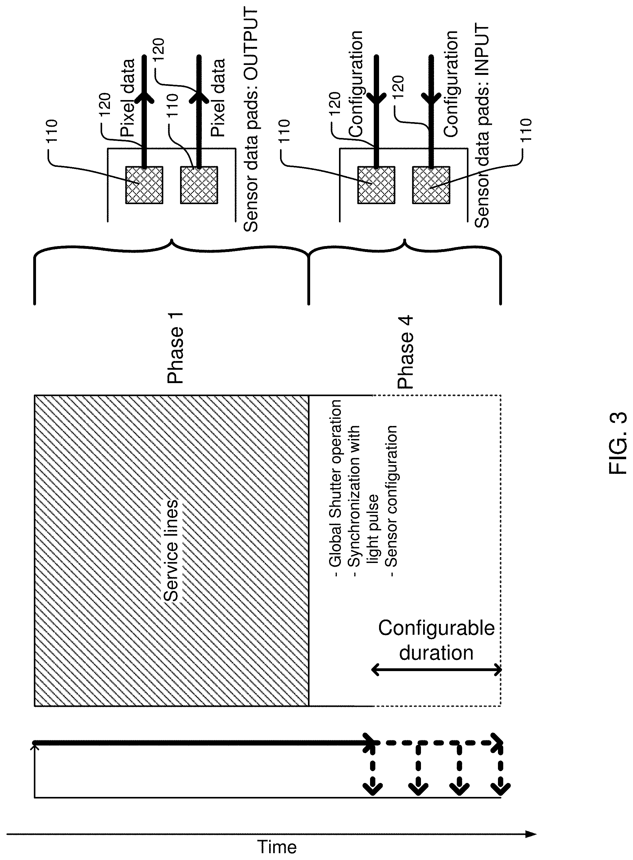
Referring now to the figures, FIG. 1 illustrates the internal timing of an embodiment of a minimal area custom CMOS image sensor. Each frame period may comprise 4 distinct phases. During phases 1 and 3, data may be issued from the sensor through sensor data pads 150, which are not signal samples from physical pixels. Rather they are data concerned with the synchronization of the chip to the camera system and for data locking. Phase 2 is concerned with the sensor rolling readout (internal timing, synchronization and readout of physical pixels) while phase 4 is for the purpose of sensor configuration. During the configuration phase, the sensor output data lines 160 may be reversed to accept incoming configuration commands. There is a risk that during phase 4, the CDR circuit in the camera unit will become unlocked, since the sensor will not send any data transitions during a defined period of time. The service lines of phase 1 may be used to send a continuous stream of data transitions, however, to re-lock the camera unit CDR circuit, should they be required.
FIG. 2 illustrates an example of such a stream where a clock-like signal is inserted into the output data stream, where normally there would be pixel data (clock recovery lines) 210. It should be noted that other clock patterns may be used and fall within the scope of this disclosure. As seen best in FIG. 2, a line header 222 may be defined, in order for the camera system to differentiate between clock recovery lines and pixel data lines. The number of clock recovery lines in phase 1 is adjustable via a register setting.
It should be noted that the duration of phase 4 may be below about .about.5 ms -10 ms, which allows for a very limited number of clock recovery lines. Therefore, the number of transitions available to re-lock the system may be correspondingly low. This should not normally be an issue, however, because the PLL voltage of the camera unit CDR does not have time to drift very far away from the locking voltage during phase 4. In the event of the PLL voltage being significantly far from the locking voltage (at start-up for example), the receiver needs a significantly greater number of transitions. For that purpose, the sensor can be programmed to be in a full clock training sequence wherein phases 1, 2 and 3 may be merged to become continuous period of clock training. See, for example, FIG. 3. Once the camera unit CDR has locked, the sensor may resume normal operation with phase 1 providing the smaller adjustments needed for re-locking of the camera unit CDR. Therefore, the CDR specification regarding the minimal number of transitions to lock or re-lock is taken care of by the 2 operation modes described.
In order to address the CDR specification concerned with the maximal number of bits between transitions (to ensure that the CDR does not lose its lock), a method which is based upon a special encoding of the pixel data, may be used.
In FIG. 4, an example of such a special pixel encoding is shown in which the actual pixel data values are 11 bits, (with the MSB transmitted first and the LSB, last). A 12th bit may be added to each pixel's data, which is always an inverted version of the 11th (least significant) true bit. This results in an encoding with very little overhead. A high transition rate may be obtained during the transmission of pixel data, thereby avoiding any possibility of the camera unit CDR becoming unlocked.
FIGS. 5A and 5B illustrate two conventional methods to generate a clock signal for an image sensor 505. FIG. 5A relates to an off-chip device that may be a crystal oscillator and a Phase Lock Loop (PLL) circuit. Although very precise, this method adds the burden of one pad 510 and one active component. Moreover the active component may require low speed control programming that further increases the conductor count. This may be a disadvantage at the distal tip of an endoscope where space is very limited. FIG. 5B represents a clock generation using on-chip circuitry. This method provides an advantageous result in terms of pad 510 and conductor counts. However, such circuits may be inconsistent and exhibit significant variability from chip to chip. Moreover, they are often temperature dependent and can be sensitive to any change in temperature. These drawbacks prevent use in applications like video where the frame rate needs to be ultra-precise.
This disclosure describes a method and system of generating an on-chip precise clock without adding any external components. It should be further noted that by virtue of re-purposing the sensor data output pads and low speed control programming pads (which may be the same bidirectional pads as described above), no extra pad nor conductor is required.
FIG. 6 depicts a conventional PLL 600. The VCDL (voltage controlled delay line) clock is compared to the incoming clock with the frequency detector and up-pushes or down-pushes are issued to the external VCO (voltage controlled oscillator) depending on the frequency detector comparison result. This system may dynamically react and adjust to ensure that the VCDL clock always matches the input clock.
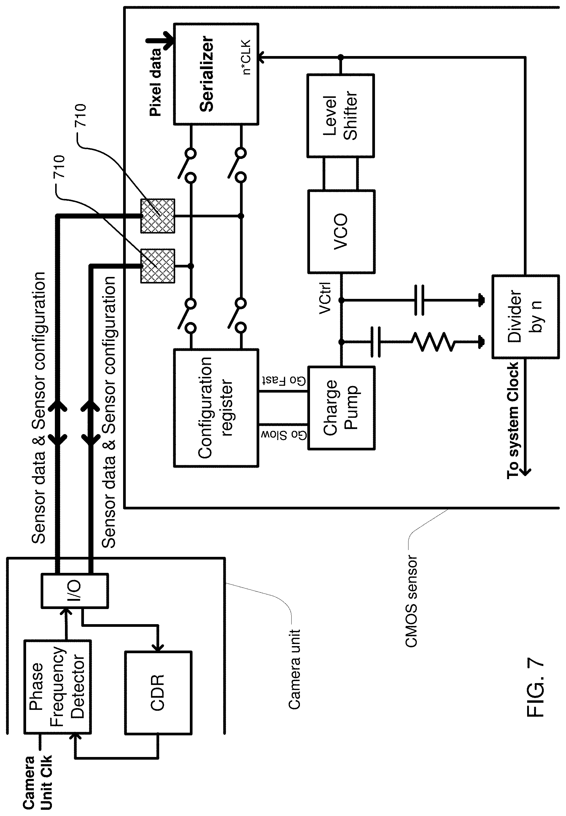
The concept behind the system and method is to create a PLL that overlaps between the sensor and the camera unit, taking advantage of the communication protocol that already exists between the two devices. In an embodiment, the system and method may move the frequency detector from the sensor PLL to the camera unit. Its input can then be attached to the precise clock provided by camera unit oscillator. This local oscillator has the additional benefit of not increasing the sensor pad count because located in the camera unit. In the embodiment, a digital feed-forward and feedback nodes in the PLL may be selected and matched to the feed-forward system node (low speed control programming from camera unit to sensor) and feedback system node (pixel data output from sensor to camera unit).
In the embodiment of FIG. 7, the feed-forward node may be chosen to be the go-fast go-slow signals and will be updated using the sensor low speed control programming. The feedback node may be chosen to be the multiplied clock prior to the divider by n. This multiplied frequency may be used to serialize the pixel data and is decoded by the CDR in the camera unit, which can then be fed back to the frequency detector. Such an embodiment does not increase the pad 710 count or the conductor count.
In an implementation, shown in FIG. 8, a DAC 808 instead of charge pump may be used. The low speed control could program a configuration register with a digital word (if using a DAC) instead of a push-up/push-down (if using a charge pump).
It may be desirable to build such a system without segmenting the on-chip PLL. The embodiment of FIG. 9 depicts an equivalent circuit where the internal PLL remains unchanged, but the clock input pad is removed and the input clock signal is provided by a clock generator distributed circuit equivalent to that of FIG. 7. The version of this last circuit using a DAC 1010 instead of a charge pump 909 is shown in FIG. 10.
In an embodiment, an algorithm that may reside in the camera unit is depicted in FIG. 11, and may be built for a charge pump based system. The Table in FIG. 12 lists the signals and parameters that may be used by the camera unit for the FIG. 11 algorithm.
The following is an example of the algorithm implementation. The R_CLK may be compared to the target frequency using REF_CLK as the method or mode of comparison. If R_CLK is too low then PUSH UP may be asserted. If R_CLK is too high then PUSH DOWN may be asserted. The BIG_LITTLE output may be used based on how far R_CLK is from the target frequency. As an example, if a big push represents a 5% change and a little push represents a 1% change in frequency then if R_CLK is lower than target frequency minus 3%, the block may issue a PUSH UP BIG command. The next time the R_CLK is measured it will be approximately 2% greater than the target and so the block may issue a PUSH DOWN LITTLE command.
The method of comparing the R_CLK to the target frequency may be as follows. In an example, if the REF_CLK is 27 MHz, the target is 40 MHz and the R_CLK is 38 MHz, then the block may count the number of R_CLK transitions over 1 ms (or 27,000 transitions of REF_CLK). It may compare its counter value, now 38,000 to the desired target of 40,000 and issue a PUSH UP BIG command assuming the BIG and LITTLE thresholds are 5% and 1%.
It will be appreciated that implementations of the disclosure may comprise or utilize a special purpose or general-purpose computer including computer hardware, such as, for example, one or more processors and system memory, as discussed in greater detail below. Implementations within the scope of the disclosure may also include physical and other computer-readable media for carrying or storing computer-executable instructions and/or data structures. Such computer-readable media can be any available media that can be accessed by a general purpose or special purpose computer system. Computer-readable media that store computer-executable instructions may be computer storage media (devices). Computer-readable media that carry computer-executable instructions may be transmission media. Thus, by way of example, and not limitation, implementations of the disclosure can comprise at least two distinctly different kinds of computer-readable media: computer storage media (devices) and transmission media.
Computer storage media (devices) includes RAM, ROM, EEPROM, CD-ROM, solid state drives ("SSDs") (e.g., based on RAM), Flash memory, phase-change memory ("PCM"), other types of memory, other optical disk storage, magnetic disk storage or other magnetic storage devices, or any other medium which can be used to store desired program code means in the form of computer-executable instructions or data structures and which can be accessed by a general purpose or special purpose computer.
A "network" may be defined as one or more data links that enable the transport of electronic data between computer systems and/or modules and/or other electronic devices. In an implementation, a sensor and camera control unit may be networked in order to communicate with each other, and other components, connected over the network to which they may be connected. When information is transferred or provided over a network or another communications connection (either hardwired, wireless, or a combination of hardwired or wireless) to a computer, the computer properly views the connection as a transmission medium. Transmissions media can include a network and/or data links which can be used to carry desired program code means in the form of computer-executable instructions or data structures and which can be accessed by a general purpose or special purpose computer. Combinations of the above should also be included within the scope of computer-readable media.
Further, upon reaching various computer system components, program code means in the form of computer-executable instructions or data structures that can be transferred automatically from transmission media to computer storage media (devices) (or vice versa). For example, computer-executable instructions or data structures received over a network or data link can be buffered in RAM within a network interface module (e.g., a "NIC"), and then eventually transferred to computer system RAM and/or to less volatile computer storage media (devices) at a computer system. RAM can also include solid state drives (SSDs or PCIx based real time memory tiered Storage, such as FusionIO). Thus, it should be understood that computer storage media (devices) can be included in computer system components that also (or even primarily) utilize transmission media.
Computer-executable instructions comprise, for example, instructions and data which, when executed at a processor, cause a general purpose computer, special purpose computer, or special purpose processing device to perform a certain function or group of functions. The computer executable instructions may be, for example, binaries, intermediate format instructions such as assembly language, or even source code. Although the subject matter has been described in language specific to structural features and/or methodological acts, it is to be understood that the subject matter defined in the appended disclosure is not necessarily limited to the described features or acts described above. Rather, the described features and acts may be disclosed as example forms of implementing the disclosure.
Those skilled in the art will appreciate that the disclosure may be practiced in network computing environments with many types of computer system configurations, including, personal computers, desktop computers, laptop computers, message processors, control units, camera control units, hand-held devices, hand pieces, multi-processor systems, microprocessor-based or programmable consumer electronics, network PCs, minicomputers, mainframe computers, mobile telephones, PDAs, tablets, pagers, routers, switches, various storage devices, and the like. It should be noted that any of the above mentioned computing devices may be provided by or located within a brick and mortar location. The disclosure may also be practiced in distributed system environments where local and remote computer systems, which may be linked (either by hardwired data links, wireless data links, or by a combination of hardwired and wireless data links) through a network, both perform tasks. In a distributed system environment, program modules may be located in both local and remote memory storage devices.
Further, where appropriate, functions described herein can be performed in one or more of: hardware, software, firmware, digital components, or analog components. For example, one or more application specific integrated circuits (ASICs) or field programmable gate arrays can be programmed to carry out one or more of the systems and procedures described herein. Certain terms may be used throughout the following description and Disclosure to refer to particular system components. As one skilled in the art will appreciate, components may be referred to by different names. This document does not intend to distinguish between components that differ in name, but not function.
FIG. 13 is a block diagram illustrating an example computing device 1300. Computing device 1300 may be used to perform various procedures, such as those discussed herein. Computing device 1300 can function as a server, a client, or any other computing entity. Computing device can perform various monitoring functions as discussed herein, and can execute one or more application programs, such as the application programs described herein. Computing device 1300 can be any of a wide variety of computing devices, such as a desktop computer, a notebook computer, a server computer, a handheld computer, camera control unit, tablet computer and the like.
Computing device 1300 includes one or more processor(s) 1302, one or more memory device(s) 1304, one or more interface(s) 1306, one or more mass storage device(s) 1308, one or more Input/Output (I/O) device(s) 1310, and a display device 1330 all of which may be coupled to a bus 1312. Processor(s) 1302 include one or more processors or controllers that execute instructions stored in memory device(s) 1304 and/or mass storage device(s) 1308. Processor(s) 1302 may also include various types of computer-readable media, such as cache memory.
Memory device(s) 1304 include various computer-readable media, such as volatile memory (e.g., random access memory (RAM) 1314) and/or nonvolatile memory (e.g., read-only memory (ROM) 1316). Memory device(s) 1304 may also include rewritable ROM, such as Flash memory.
Mass storage device(s) 1308 include various computer readable media, such as magnetic tapes, magnetic disks, optical disks, solid-state memory (e.g., Flash memory), and so forth. As shown in FIG. 13, a particular mass storage device is a hard disk drive 1324. Various drives may also be included in mass storage device(s) 1308 to enable reading from and/or writing to the various computer readable media. Mass storage device(s) 1308 include removable media 1326 and/or non-removable media.
I/O device(s) 1310 include various devices that allow data and/or other information to be input to or retrieved from computing device 1300. Example I/O device(s) 1310 include digital imaging devices, electromagnetic sensors and emitters, cursor control devices, keyboards, keypads, microphones, monitors or other display devices, speakers, printers, network interface cards, modems, lenses, CCDs or other image capture devices, and the like.
Display device 1330 includes any type of device capable of displaying information to one or more users of computing device 1300. Examples of display device 1330 include a monitor, display terminal, video projection device, and the like.
Interface(s) 1306 include various interfaces that allow computing device 1300 to interact with other systems, devices, or computing environments. Example interface(s) 1306 may include any number of different network interfaces 1320, such as interfaces to local area networks (LANs), wide area networks (WANs), wireless networks, and the Internet. Other interface(s) include user interface 1318 and peripheral device interface 1322. The interface(s) 1306 may also include one or more user interface elements 1318. The interface(s) 1306 may also include one or more peripheral interfaces such as interfaces for printers, pointing devices (mice, track pad, etc.), keyboards, and the like.
Bus 1312 allows processor(s) 1302, memory device(s) 1304, interface(s) 1306, mass storage device(s) 1308, and I/O device(s) 1310 to communicate with one another, as well as other devices or components coupled to bus 1312. Bus 1312 represents one or more of several types of bus structures, such as a system bus, PCI bus, IEEE 1394 bus, USB bus, and so forth.
For purposes of illustration, programs and other executable program components may be shown herein as discrete blocks, although it is understood that such programs and components may reside at various times in different storage components of computing device 1300, and may be executed by processor(s) 1302. Alternatively, the systems and procedures described herein can be implemented in hardware, or a combination of hardware, software, and/or firmware. For example, one or more application specific integrated circuits (ASICs) can be programmed to carry out one or more of the systems and procedures described herein.
It will be appreciated that the disclosure may be used with any image sensor, whether a CMOS image sensor or CCD image sensor, without departing from the scope of the disclosure. Further, the image sensor may be located in any location within the overall system, including, but not limited to, the tip of the endoscope, the hand piece of the imaging device or camera, the control unit, or any other location within the system without departing from the scope of the disclosure.
Implementations of an image sensor that may be utilized by the disclosure include, but are not limited to, the following, which are merely examples of various types of sensors that may be utilized by the disclosure.
FIGS. 14A and 14B illustrate an implementation of a monolithic sensor 1405 having a plurality of pixel arrays 1410 for producing a three dimensional image in accordance with the teachings and principles of the disclosure. Such an implementation may be desirable for three dimensional image capture, wherein the two pixel arrays 1410 may be offset during use. In another implementation, a first pixel array 1410 and a second pixel array 1410 may be dedicated to receiving a predetermined range of wave lengths of electromagnetic radiation, wherein the first pixel array 1410 is dedicated to a different range of wave length electromagnetic radiation than the second pixel array 1410.
FIGS. 15A and 15B illustrate a view of an implementation of an imaging sensor built on a plurality of substrates 1510, 1511. As illustrated, a plurality of pixel columns forming the pixel array 1515 are located on the first substrate 1511 and a plurality of circuit columns 1520 are located on a second substrate 1510. Also illustrated in the figure are the electrical connection and communication between one column of pixels to its associated or corresponding column of circuitry.
In one implementation, an image sensor, which might otherwise be manufactured with its pixel array and supporting circuitry on a single, monolithic substrate/chip, may have the pixel array separated from all or a majority of the supporting circuitry. The disclosure may use at least two substrates/chips, which will be stacked together using three-dimensional stacking technology. The first of the two substrates/chips may be processed using an image CMOS process. The first substrate/chip may be comprised either of a pixel array exclusively or a pixel array surrounded by limited circuitry. The second or subsequent substrate/chip may be processed using any process, and does not have to be from an image CMOS process. The second substrate/chip may be, but is not limited to, a highly dense digital process in order to integrate a variety and number of functions in a very limited space or area on the substrate/chip, or a mixed-mode or analog process in order to integrate for example precise analog functions, or a RF process in order to implement wireless capability, or MEMS (Micro-Electro-Mechanical Systems) in order to integrate MEMS devices. The image CMOS substrate/chip may be stacked with the second or subsequent substrate/chip using any three-dimensional technique. The second substrate/chip may support most, or a majority, of the circuitry that would have otherwise been implemented in the first image CMOS chip (if implemented on a monolithic substrate/chip) as peripheral circuits and therefore have increased the overall system area while keeping the pixel array size constant and optimized to the fullest extent possible. The electrical connection between the two substrates/chips may be done through interconnects, which may be wirebonds, bump and/or TSV (Through Silicon Via).
FIGS. 16A and 16B illustrate a view of an implementation of an imaging sensor having a plurality of pixel arrays for producing a three dimensional image. The three dimensional image sensor may be built on a plurality of substrates 1611a, 1611b, 1611c, and may comprise the plurality of pixel arrays 1615a, 1615b and other associated circuitry 1630a, 1630b, wherein a plurality of pixel columns forming the first pixel array and a plurality of pixel columns forming a second pixel array are located on respective substrates and a plurality of circuit columns are located on a separate substrate. Also illustrated are the electrical connections and communications between columns of pixels to associated or corresponding column of circuitry.
It will be appreciated that the teachings and principles of the disclosure may be used in a reusable device platform, a limited use device platform, a re-posable use device platform, or a single-use/disposable device platform without departing from the scope of the disclosure. It will be appreciated that in a re-usable device platform an end-user is responsible for cleaning and sterilization of the device. In a limited use device platform the device can be used for some specified amount of times before becoming inoperable. Typical new device is delivered sterile with additional uses requiring the end-user to clean and sterilize before additional uses. In a re-posable use device platform a third-party may reprocess the device (e.g., cleans, packages and sterilizes) a single-use device for additional uses at a lower cost than a new unit. In a single-use/disposable device platform a device is provided sterile to the operating room and used only once before being disposed of.
Additionally, the teachings and principles of the disclosure may include any and all wavelengths of electromagnetic energy, including the visible and non-visible spectrums, such as infrared (IR), ultraviolet (UV), and X-ray.
It will be appreciated that various features disclosed herein provide significant advantages and advancements in the art. The following embodiments may be exemplary of some of those features.
An embodiment of a reduced area image sensor may comprise: input and output pads wherein the pad count is reduced by no having a no synchronization clock pad; wherein signal transitions are encoded within the output data; service lines within the frame; wherein a camera unit clock and/or data recovery circuit may be used to lock on the incoming sensor data to keep it synchronized. An embodiment may further comprise a minimal area CMOS image sensor disposed within the distal end of endoscopes. An embodiment may further comprise at least one transition within each pixel serial data created within the pixel array. An embodiment may further comprise at least one transition during a series of a plurality pixel data sets created by the pixel array. An embodiment may further comprise a plurality of transitions within each pixel serial data created by the pixel array. An embodiment may further comprise replaced pixel data with clock signal data. An embodiment may further comprise replaced pixel data with clock signal data within at least one service line phase of one frame period. An embodiment may further comprise replaced pixel data with clock signal data within the service line phase just prior to the true pixel data output phase. An embodiment may further comprise replaced pixel data with clock signal data within and at all output frame phases except during pixel data output phase.
An embodiment of a reduced image sensor may operate, be designed by, and may comprise: replacing pixel data with clock signal data within, and at all output frame phases including during pixel data output phase; removing clock pads; building a Phase Lock Loop (PLL) with blocks of the sensor and other blocks of the camera unit; using data lines and configuration lines for connecting together sensor PLL blocks and camera unit PLL blocks; and using the camera unit clock and data recovery circuit to lock on the incoming sensor data. An embodiment may further comprise minimal area CMOS image sensor for use in the distal end of endoscopes. An embodiment may further comprise bidirectional data pads to issue image data during a defined portion of the frame timing. An embodiment may further issue other types of data during another portions of the frame data output. An embodiment may switch direction and receive commands from the external camera system during a third defined time period during the frame while in receive mode. An embodiment may be PLL based on a charge pump for driving the Voltage Controlled Oscillator (VCO). An embodiment may be PLL based on a Digital to Analog Convertor (DAC) for driving the VCO. An embodiment may further comprise programming a sensor configuration register to store increase of decrease of the resultant operating frequency. An embodiment may further comprise local oscillator as a PLL reference clock. An embodiment may further comprise the use differing strength pushes.
In the foregoing Detailed Description of the Disclosure, various features of the disclosure may be grouped together in a single embodiment for the purpose of streamlining the disclosure. This method of disclosure is not to be interpreted as reflecting an intention that the disclosure requires more features than may be expressly recited in the disclosure. Rather, inventive aspects lie in less than all features of a single foregoing disclosed embodiment.
It is to be understood that the above-described arrangements may be only illustrative of the application of the principles of the disclosure. Numerous modifications and alternative arrangements may be devised by those skilled in the art without departing from the spirit and scope of the disclosure and the appended disclosure may be intended to cover such modifications and arrangements.
Thus, while the disclosure has been shown in the drawings and described above with particularity and detail, it will be apparent to those of ordinary skill in the art that numerous modifications, including, but not limited to, variations in size, materials, shape, form, function and manner of operation, assembly and use may be made without departing from the principles and concepts set forth herein.
Further, where appropriate, functions described herein can be performed in one or more of: hardware, software, firmware, digital components, or analog components. For example, one or more application specific integrated circuits (ASICs) can be programmed to carry out one or more of the systems and procedures described herein. Certain terms may be used throughout the following description and Disclosure to refer to particular system components. As one skilled in the art will appreciate, components may be referred to by different names. This document does not intend to distinguish between components that differ in name, but not function.
The foregoing description has been presented for the purposes of illustration and description. It is not intended to be exhaustive or to limit the disclosure to the precise form disclosed. Many modifications and variations may be possible in light of the above teaching. Further, it should be noted that any or all of the aforementioned alternate implementations may be used in any combination desired to form additional hybrid implementations of the disclosure.
Further, although specific implementations of the disclosure have been described and illustrated, the disclosure is not to be limited to the specific forms or arrangements of parts so described and illustrated. The scope of the disclosure is to be defined by the disclosure appended hereto, any future disclosure submitted here and in different applications, and their equivalents.
* * * * *
D00000
D00001
D00002
D00003
D00004
D00005
D00006
D00007
D00008
D00009
D00010
D00011
D00012

D00013
D00014
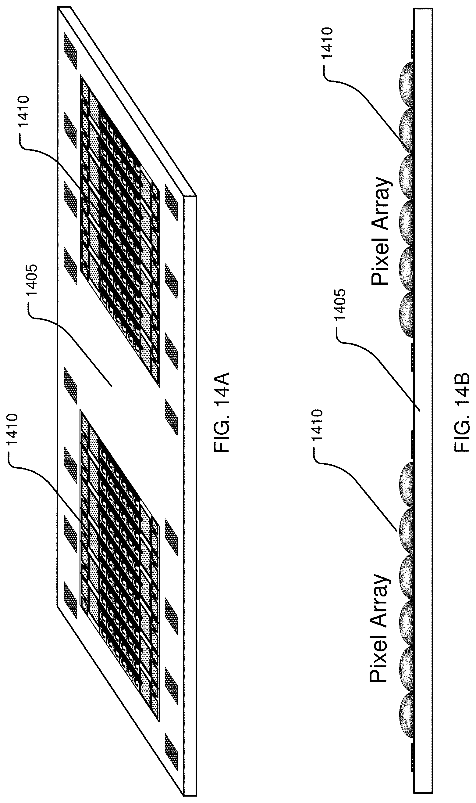
D00015

D00016

XML
uspto.report is an independent third-party trademark research tool that is not affiliated, endorsed, or sponsored by the United States Patent and Trademark Office (USPTO) or any other governmental organization. The information provided by uspto.report is based on publicly available data at the time of writing and is intended for informational purposes only.
While we strive to provide accurate and up-to-date information, we do not guarantee the accuracy, completeness, reliability, or suitability of the information displayed on this site. The use of this site is at your own risk. Any reliance you place on such information is therefore strictly at your own risk.
All official trademark data, including owner information, should be verified by visiting the official USPTO website at www.uspto.gov. This site is not intended to replace professional legal advice and should not be used as a substitute for consulting with a legal professional who is knowledgeable about trademark law.