Minimize image sensor I/O and conductor counts in endoscope applications
Blanquart A
U.S. patent number 10,750,933 [Application Number 14/214,794] was granted by the patent office on 2020-08-25 for minimize image sensor i/o and conductor counts in endoscope applications. This patent grant is currently assigned to DePuy Synthes Products, Inc.. The grantee listed for this patent is Depuy Synthes Products, Inc.. Invention is credited to Laurent Blanquart.


View All Diagrams
| United States Patent | 10,750,933 |
| Blanquart | August 25, 2020 |
Minimize image sensor I/O and conductor counts in endoscope applications
Abstract
The disclosure extends to systems and methods for reducing the area of an image sensor by employing bi-directional pads used for both image data issuance and configuration command reception and internal supply voltage generation, for reducing the number of conductors in an endoscope system.
| Inventors: | Blanquart; Laurent (Westlake Village, CA) | ||||||||||
|---|---|---|---|---|---|---|---|---|---|---|---|
| Applicant: |
|
||||||||||
| Assignee: | DePuy Synthes Products, Inc.
(Raynham, MA) |
||||||||||
| Family ID: | 51530287 | ||||||||||
| Appl. No.: | 14/214,794 | ||||||||||
| Filed: | March 15, 2014 |
Prior Publication Data
| Document Identifier | Publication Date | |
|---|---|---|
| US 20140275783 A1 | Sep 18, 2014 | |
Related U.S. Patent Documents
| Application Number | Filing Date | Patent Number | Issue Date | ||
|---|---|---|---|---|---|
| 61791547 | Mar 15, 2013 | ||||
| 61790590 | Mar 15, 2013 | ||||
| Current U.S. Class: | 1/1 |
| Current CPC Class: | A61B 1/00124 (20130101); A61B 1/00018 (20130101); A61B 1/00066 (20130101); H04N 5/23203 (20130101); A61B 1/051 (20130101); A61B 1/053 (20130101); A61B 1/00055 (20130101); A61B 1/00006 (20130101); H04N 5/3532 (20130101); H04N 13/239 (20180501); H04N 2005/2255 (20130101) |
| Current International Class: | A61B 1/04 (20060101); A61B 1/00 (20060101); A61B 1/05 (20060101); H04N 5/232 (20060101); H04N 13/239 (20180101); H04N 5/353 (20110101); H04N 5/225 (20060101) |
| Field of Search: | ;348/68 |
References Cited [Referenced By]
U.S. Patent Documents
| 3796220 | March 1974 | Bredemeier |
| 3858577 | January 1975 | Bass et al. |
| 4011403 | March 1977 | Epstein et al. |
| 4153356 | May 1979 | Hama |
| 4350150 | September 1982 | Kubota et al. |
| 4363963 | December 1982 | Ando |
| 4429686 | February 1984 | Hosoda |
| 4433675 | February 1984 | Konoshima |
| 4436095 | March 1984 | Kruger |
| 4561430 | December 1985 | Walsh |
| 4572164 | February 1986 | Yoshida et al. |
| 4589404 | May 1986 | Barath et al. |
| 4600940 | July 1986 | Sluyter |
| 4604992 | August 1986 | Sato |
| 4670653 | June 1987 | McConkle et al. |
| 4740837 | April 1988 | Yanagisawa et al. |
| 4741327 | May 1988 | Yabe |
| 4745471 | May 1988 | Takamura et al. |
| 4773396 | September 1988 | Okazaki |
| 4786965 | November 1988 | Yabe |
| 4800424 | January 1989 | Noguchi |
| 4831444 | May 1989 | Kato |
| 4832003 | May 1989 | Yabe |
| 4845555 | July 1989 | Yabe et al. |
| 4853772 | August 1989 | Kikuchi |
| 4866526 | September 1989 | Ams et al. |
| 4888639 | December 1989 | Yabe et al. |
| 4918521 | April 1990 | Yabe et al. |
| 4938205 | July 1990 | Nudelman |
| 4942473 | July 1990 | Zeevi et al. |
| 4953539 | September 1990 | Nakamura et al. |
| 4954878 | September 1990 | Fox et al. |
| 5010038 | April 1991 | Fox et al. |
| 5010876 | April 1991 | Henley et al. |
| 5016975 | May 1991 | Sasaki et al. |
| 5021888 | June 1991 | Kondou et al. |
| 5042915 | August 1991 | Akutsu et al. |
| 5065444 | November 1991 | Garber |
| RE33854 | March 1992 | Adair |
| 5103497 | April 1992 | Hicks |
| 5111804 | May 1992 | Funakoshi |
| 5115309 | May 1992 | Hang |
| 5133035 | July 1992 | Hicks |
| 5168361 | December 1992 | Hackmann |
| 5168863 | December 1992 | Kurtzer |
| 5187572 | February 1993 | Nakamura et al. |
| 5188094 | February 1993 | Adair |
| 5200838 | April 1993 | Nudelman et al. |
| 5220198 | June 1993 | Tsuji |
| 5227662 | July 1993 | Ohno et al. |
| 5228430 | July 1993 | Sakamoto |
| 5237403 | August 1993 | Sugimoto et al. |
| 5241170 | August 1993 | Field, Jr. et al. |
| 5277172 | January 1994 | Sugimoto |
| 5289555 | February 1994 | Sanso |
| 5307804 | May 1994 | Bonnet |
| 5313306 | May 1994 | Kuban et al. |
| 5325847 | July 1994 | Matsuno |
| 5339275 | August 1994 | Hyatt |
| 5381784 | January 1995 | Adair |
| 5400267 | March 1995 | Denen et al. |
| 5402768 | April 1995 | Adair |
| 5411020 | May 1995 | Ito |
| 5427087 | June 1995 | Ito et al. |
| 5454366 | October 1995 | Ito et al. |
| 5461425 | October 1995 | Fowler et al. |
| 5471515 | November 1995 | Fossum et al. |
| 5489801 | February 1996 | Blish, II |
| 5494483 | February 1996 | Adair |
| 5522006 | May 1996 | Takeuchi et al. |
| 5550595 | August 1996 | Hannah |
| 5576781 | November 1996 | Deleeuw |
| 5594282 | January 1997 | Otsuki |
| 5594497 | January 1997 | Ahern et al. |
| 5614763 | March 1997 | Womack |
| 5665959 | September 1997 | Fossum et al. |
| 5721422 | February 1998 | Bird |
| 5734418 | March 1998 | Danna |
| 5748234 | May 1998 | Lippincott |
| 5754313 | May 1998 | Pelchy et al. |
| 5757075 | May 1998 | Kitaoka |
| 5784099 | July 1998 | Lippincott |
| 5787298 | July 1998 | Broedner et al. |
| 5841126 | November 1998 | Fossum et al. |
| 5857963 | January 1999 | Pelchy et al. |
| 5879289 | March 1999 | Yarush et al. |
| 5887049 | March 1999 | Fossum |
| 5896166 | April 1999 | D'Alfonso et al. |
| 5907178 | May 1999 | Baker et al. |
| 5929901 | July 1999 | Adair et al. |
| 5949483 | September 1999 | Fossum et al. |
| 5986693 | November 1999 | Adair et al. |
| 5990506 | November 1999 | Fossum et al. |
| 6005619 | December 1999 | Fossum |
| 6021172 | February 2000 | Fossum et al. |
| 6027955 | February 2000 | Lee et al. |
| 6028330 | February 2000 | Lee et al. |
| 6043839 | March 2000 | Adair et al. |
| 6059776 | May 2000 | Gatto |
| 6059793 | May 2000 | Pagedas |
| 6073043 | June 2000 | Schneider |
| 6096573 | August 2000 | Chen |
| 6101232 | August 2000 | Fossum et al. |
| 6118142 | September 2000 | Chen et al. |
| 6139489 | October 2000 | Wampler et al. |
| 6142930 | November 2000 | Ito et al. |
| 6144542 | November 2000 | Ker |
| 6166367 | December 2000 | Cho |
| 6166768 | December 2000 | Fossum et al. |
| 6180969 | January 2001 | Yang et al. |
| 6184055 | February 2001 | Yang et al. |
| 6194260 | February 2001 | Chien et al. |
| 6198087 | March 2001 | Boon |
| 6207984 | March 2001 | Chang |
| 6211904 | April 2001 | Adair et al. |
| 6215517 | April 2001 | Takahashi et al. |
| 6239456 | May 2001 | Berezin et al. |
| 6242277 | June 2001 | Lin et al. |
| 6255681 | July 2001 | Osadchy et al. |
| 6272269 | August 2001 | Naum |
| 6275255 | August 2001 | Adair et al. |
| 6294775 | September 2001 | Seibel et al. |
| 6303421 | October 2001 | Chang |
| 6310642 | October 2001 | Adair et al. |
| 6313868 | November 2001 | D'Alfonso et al. |
| 6320630 | November 2001 | Yamashita et al. |
| 6327493 | December 2001 | Ozawa et al. |
| 6331156 | December 2001 | Haefele et al. |
| 6333205 | December 2001 | Rhodes |
| 6369812 | April 2002 | Iyriboz et al. |
| 6387043 | May 2002 | Yoon |
| 6388243 | May 2002 | Berezin et al. |
| 6390972 | May 2002 | Speier et al. |
| 6400824 | June 2002 | Mansoorian et al. |
| 6404048 | June 2002 | Akram |
| 6410377 | June 2002 | Hwang et al. |
| 6416463 | July 2002 | Tsuzuki et al. |
| 6419626 | July 2002 | Yoon |
| 6419627 | July 2002 | Ben Nun |
| 6424369 | July 2002 | Adair et al. |
| 6436032 | August 2002 | Eto et al. |
| 6441482 | August 2002 | Foster |
| 6452626 | September 2002 | Adair et al. |
| 6456326 | September 2002 | Fossum et al. |
| 6469739 | October 2002 | Bechtel et al. |
| 6485414 | November 2002 | Neuberger |
| 6512280 | January 2003 | Chen et al. |
| 6515321 | February 2003 | Jwo |
| 6549235 | April 2003 | Fossum et al. |
| 6555842 | April 2003 | Fossum et al. |
| 6570617 | May 2003 | Fossum et al. |
| 6588884 | July 2003 | Furlani et al. |
| 6606122 | August 2003 | Shaw et al. |
| 6610557 | August 2003 | Lee et al. |
| 6627474 | September 2003 | Barna et al. |
| 6659940 | December 2003 | Adler |
| 6665013 | December 2003 | Fossum et al. |
| 6690466 | February 2004 | Miller et al. |
| 6692431 | February 2004 | Kazakevich |
| 6704049 | March 2004 | Fossum |
| 6720810 | April 2004 | New |
| 6726620 | April 2004 | Shibata et al. |
| 6730900 | May 2004 | Hsish et al. |
| 6740870 | May 2004 | Doudoumopoulos |
| 6744068 | June 2004 | Fossum et al. |
| 6773392 | August 2004 | Kikuchi et al. |
| 6784940 | August 2004 | Takazawa et al. |
| 6796939 | September 2004 | Hirata et al. |
| 6799065 | September 2004 | Niemeyer |
| 6809358 | October 2004 | Hsieh et al. |
| 6812949 | November 2004 | Switzer et al. |
| 6838653 | January 2005 | Campbell et al. |
| 6838716 | January 2005 | Asada et al. |
| 6856712 | February 2005 | Fauver et al. |
| 6862036 | March 2005 | Adair et al. |
| 6879340 | April 2005 | Chevallier |
| 6897082 | May 2005 | Rhodes et al. |
| 6899675 | May 2005 | Cline et al. |
| 6921920 | July 2005 | Kazakevich |
| 6943838 | September 2005 | Komoro et al. |
| 6947090 | September 2005 | Komoro et al. |
| 6961461 | November 2005 | MacKinnon et al. |
| 6970195 | November 2005 | Bidermann et al. |
| 6976954 | December 2005 | Takahashi |
| 6982740 | January 2006 | Adair et al. |
| 6982742 | January 2006 | Adair et al. |
| 6997871 | February 2006 | Sonnenschein et al. |
| 6999118 | February 2006 | Suzuki |
| 7002231 | February 2006 | Rhodes et al. |
| 7002621 | February 2006 | Adair et al. |
| 7009634 | March 2006 | Iddan et al. |
| 7009646 | March 2006 | Fossum et al. |
| 7018331 | March 2006 | Chang et al. |
| 7027092 | April 2006 | Altree |
| 7030904 | April 2006 | Adair et al. |
| 7037259 | May 2006 | Hakamata et al. |
| 7061117 | June 2006 | Yang et al. |
| 7068878 | June 2006 | Crossman-Bosworth et al. |
| 7070560 | July 2006 | Takashi et al. |
| 7088398 | August 2006 | Wolf et al. |
| 7102682 | September 2006 | Baer |
| 7105371 | September 2006 | Fossum et al. |
| 7106367 | September 2006 | Sarwari |
| 7106377 | September 2006 | Bean et al. |
| 7115091 | October 2006 | Root et al. |
| 7129108 | October 2006 | Jang |
| 7183129 | February 2007 | Lee |
| 7184084 | February 2007 | Glenn |
| 7189226 | March 2007 | Auld et al. |
| 7193519 | March 2007 | Root et al. |
| 7202899 | April 2007 | Lin et al. |
| 7217967 | May 2007 | Han |
| 7227469 | June 2007 | Varner et al. |
| 7230247 | June 2007 | Shibayama |
| 7230615 | June 2007 | Wang et al. |
| 7232712 | June 2007 | Han |
| 7244920 | July 2007 | Kim et al. |
| 7250594 | July 2007 | Lin et al. |
| 7258546 | August 2007 | Beier et al. |
| 7258663 | August 2007 | Doguchi et al. |
| 7261687 | August 2007 | Yang |
| 7273452 | September 2007 | Barbato et al. |
| 7274390 | September 2007 | Sevat et al. |
| 7276785 | October 2007 | Bauer et al. |
| 7280139 | October 2007 | Pahr et al. |
| 7282025 | October 2007 | Abe |
| 7283566 | October 2007 | Siemens et al. |
| 7295578 | November 2007 | Lyle et al. |
| 7303528 | December 2007 | Couvillon, Jr. |
| 7317955 | January 2008 | McGreevy |
| 7319478 | January 2008 | Dolt et al. |
| 7331523 | February 2008 | Meier et al. |
| 7338832 | March 2008 | Park et al. |
| 7339982 | March 2008 | Wood, Jr. |
| 7354841 | April 2008 | Jeon |
| 7365768 | April 2008 | Ono et al. |
| 7368771 | May 2008 | Roh et al. |
| 7369166 | May 2008 | Fossum et al. |
| 7369176 | May 2008 | Sonnenschein et al. |
| 7386084 | June 2008 | Yin |
| 7391013 | June 2008 | Johnston et al. |
| 7397076 | July 2008 | Jang |
| 7402811 | July 2008 | Hatanaka et al. |
| 7443296 | October 2008 | Mezhinsky et al. |
| 7470893 | December 2008 | Suzuki et al. |
| 7488637 | February 2009 | Kim |
| 7511257 | March 2009 | Lee et al. |
| 7517351 | April 2009 | Culp et al. |
| 7522341 | April 2009 | Mouli |
| 7525168 | April 2009 | Hsieh |
| 7534645 | May 2009 | Choi |
| 7535037 | May 2009 | Lyu |
| 7540645 | June 2009 | Kazakevich |
| 7542069 | June 2009 | Tashiro |
| 7544163 | June 2009 | MacKinnon et al. |
| 7545434 | June 2009 | Bean et al. |
| 7551059 | June 2009 | Farrier |
| 7564935 | July 2009 | Suzuki |
| 7567291 | July 2009 | Bechtel et al. |
| 7568619 | August 2009 | Todd et al. |
| 7573516 | August 2009 | Krymski et al. |
| 7578786 | August 2009 | Boulais et al. |
| 7583872 | September 2009 | Seibel et al. |
| 7589349 | September 2009 | Hong |
| 7595210 | September 2009 | Shim |
| 7598686 | October 2009 | Lys et al. |
| 7599439 | October 2009 | Lavelle et al. |
| 7605016 | October 2009 | Min |
| 7608874 | October 2009 | Lee et al. |
| 7612318 | November 2009 | Jeon |
| 7615808 | November 2009 | Pain et al. |
| 7615838 | November 2009 | Kim |
| 7616986 | November 2009 | Seibel et al. |
| 7630008 | December 2009 | Sarwari |
| 7646407 | January 2010 | Fossum et al. |
| 7663115 | February 2010 | Korthout et al. |
| 7744528 | June 2010 | Wallace et al. |
| 7749799 | July 2010 | Pain |
| 7768562 | August 2010 | Boemler |
| 7794394 | September 2010 | Frangioni |
| 7795650 | September 2010 | Eminoglu et al. |
| 7800192 | September 2010 | Venezia et al. |
| 7801584 | September 2010 | Iddan et al. |
| 7830434 | November 2010 | Li et al. |
| 7868283 | January 2011 | Mabuchi |
| 7871373 | January 2011 | Yamada |
| 7880662 | February 2011 | Bogaerts |
| 7901974 | March 2011 | Venezia et al. |
| 7914447 | March 2011 | Kanai |
| 7916193 | March 2011 | Fossum |
| 7923763 | April 2011 | Lauxtermann |
| 7935050 | May 2011 | Luanava et al. |
| 7936394 | May 2011 | Wu |
| 7944566 | May 2011 | Xie |
| 7952096 | May 2011 | Rhodes |
| 7973342 | July 2011 | Jeon |
| 7995123 | August 2011 | Lee et al. |
| 8089542 | January 2012 | Chevallier |
| 8100826 | January 2012 | MacKinnon et al. |
| 8101903 | January 2012 | Mokhnatyuk |
| 8154055 | April 2012 | Ha |
| 8159584 | April 2012 | Iwabuchi et al. |
| 8193541 | June 2012 | Maehara |
| 8212884 | July 2012 | Seibel et al. |
| 8300111 | October 2012 | Iwane |
| 8317689 | November 2012 | Remijan et al. |
| 8382662 | February 2013 | Soper et al. |
| 8384814 | February 2013 | Chevallier |
| 8396535 | March 2013 | Wang et al. |
| 8405748 | March 2013 | Mao et al. |
| 8423110 | April 2013 | Barbato et al. |
| 8426096 | April 2013 | Maezawa |
| 8471938 | June 2013 | Altice, Jr. et al. |
| 8476575 | July 2013 | Mokhnatyuk |
| 8493474 | July 2013 | Richardson |
| 8493564 | July 2013 | Brukilacchio et al. |
| 8523367 | September 2013 | Ogura |
| 8537203 | September 2013 | Seibel et al. |
| 8582011 | November 2013 | Dosluoglu |
| 8602971 | December 2013 | Farr |
| 8614754 | December 2013 | Fossum |
| 8625016 | January 2014 | Fossum et al. |
| 8629023 | January 2014 | Lee |
| 8638847 | January 2014 | Wang |
| 8648287 | February 2014 | Fossum |
| 8649848 | February 2014 | Crane et al. |
| 8668339 | March 2014 | Kabuki et al. |
| 8675125 | March 2014 | Cossairt et al. |
| 8698887 | April 2014 | Makino et al. |
| 8733660 | May 2014 | Wang et al. |
| 8754358 | June 2014 | Chou et al. |
| 8797434 | August 2014 | Lee et al. |
| 8830340 | September 2014 | Burt et al. |
| 8836834 | September 2014 | Hashimoto et al. |
| 8854517 | October 2014 | Honda et al. |
| 8858425 | October 2014 | Farr et al. |
| 8885034 | November 2014 | Adair et al. |
| 8896730 | November 2014 | Fossum |
| 8952312 | February 2015 | Blanquart et al. |
| 9066677 | June 2015 | Seto |
| 9123602 | September 2015 | Blanquart |
| 9153609 | October 2015 | Blanquart |
| 9343489 | May 2016 | Blanquart et al. |
| 9763566 | September 2017 | Blanquart |
| 9907459 | March 2018 | Blanquart |
| 10517469 | December 2019 | Blanquart et al. |
| 10517471 | December 2019 | Blanquart |
| 2001/0016804 | August 2001 | Cunningham |
| 2001/0019361 | September 2001 | Savoye |
| 2001/0030744 | October 2001 | Chang |
| 2001/0041825 | November 2001 | Shibata et al. |
| 2001/0052930 | December 2001 | Adair et al. |
| 2002/0011809 | January 2002 | Hartge et al. |
| 2002/0017611 | February 2002 | Tashiro et al. |
| 2002/0044207 | April 2002 | Dielhof et al. |
| 2002/0067408 | June 2002 | Adair et al. |
| 2002/0080248 | June 2002 | Adair et al. |
| 2002/0158986 | October 2002 | Baer |
| 2002/0163578 | November 2002 | Adair et al. |
| 2002/0180867 | December 2002 | Adair et al. |
| 2003/0007087 | January 2003 | Hakamata et al. |
| 2003/0043264 | March 2003 | Furuya et al. |
| 2003/0052983 | March 2003 | Altree |
| 2003/0107664 | June 2003 | Suzuki |
| 2003/0163029 | August 2003 | Sonnenschein et al. |
| 2003/0187586 | October 2003 | Katzenmaier et al. |
| 2003/0189663 | October 2003 | Dolt et al. |
| 2003/0218120 | November 2003 | Shibayama |
| 2004/0010196 | January 2004 | Wang et al. |
| 2004/0036010 | February 2004 | Hsieh et al. |
| 2004/0049215 | March 2004 | Snow et al. |
| 2004/0073086 | April 2004 | Abe |
| 2004/0078494 | April 2004 | Lennox et al. |
| 2004/0082833 | April 2004 | Adler et al. |
| 2004/0095495 | May 2004 | Inokuma et al. |
| 2004/0111012 | June 2004 | Whitman |
| 2004/0169771 | September 2004 | Washington et al. |
| 2004/0249267 | December 2004 | Gilboa |
| 2005/0027164 | February 2005 | Barbato et al. |
| 2005/0038322 | February 2005 | Banik |
| 2005/0075538 | April 2005 | Banik et al. |
| 2005/0131279 | June 2005 | Boulais et al. |
| 2005/0148819 | July 2005 | Noguchi et al. |
| 2005/0151866 | July 2005 | Ando et al. |
| 2005/0168941 | August 2005 | Sokol et al. |
| 2005/0174428 | August 2005 | Abe |
| 2005/0206755 | September 2005 | Yokoyama et al. |
| 2005/0222499 | October 2005 | Banik et al. |
| 2005/0231591 | October 2005 | Abe |
| 2005/0234302 | October 2005 | MacKinnon et al. |
| 2005/0237412 | October 2005 | Shiohara et al. |
| 2005/0288546 | December 2005 | Sonnenschein et al. |
| 2006/0007507 | January 2006 | Inaba et al. |
| 2006/0022234 | February 2006 | Adair et al. |
| 2006/0023109 | February 2006 | Mabuchi et al. |
| 2006/0035415 | February 2006 | Wood et al. |
| 2006/0069314 | March 2006 | Farr |
| 2006/0074289 | April 2006 | Adler et al. |
| 2006/0164533 | July 2006 | Hsieh et al. |
| 2006/0181627 | August 2006 | Farrier |
| 2006/0221230 | October 2006 | Dutta et al. |
| 2006/0249765 | November 2006 | Hsieh |
| 2006/0250513 | November 2006 | Yamamoto et al. |
| 2006/0293563 | December 2006 | Banik et al. |
| 2006/0293565 | December 2006 | Uchimura et al. |
| 2007/0002134 | January 2007 | Ishihara et al. |
| 2007/0030262 | February 2007 | Ambo et al. |
| 2007/0030345 | February 2007 | Amling et al. |
| 2007/0046803 | March 2007 | Ahn |
| 2007/0078328 | April 2007 | Ozaki et al. |
| 2007/0091190 | April 2007 | Iwabuchi et al. |
| 2007/0094303 | April 2007 | Zwingenberger et al. |
| 2007/0129601 | June 2007 | Johnston et al. |
| 2007/0138375 | June 2007 | Lee et al. |
| 2007/0153337 | July 2007 | Kim |
| 2007/0159526 | July 2007 | Abe |
| 2007/0182842 | August 2007 | Sonnenschein et al. |
| 2007/0185549 | August 2007 | Zdeblick |
| 2007/0187703 | August 2007 | Erchak |
| 2007/0197873 | August 2007 | Birnkrant |
| 2007/0225556 | September 2007 | Ortiz et al. |
| 2007/0244364 | October 2007 | Luanava et al. |
| 2007/0244365 | October 2007 | Wiklof |
| 2007/0276187 | November 2007 | Wiklof et al. |
| 2007/0297190 | December 2007 | Ng |
| 2008/0021271 | January 2008 | Pasero et al. |
| 2008/0042046 | February 2008 | Mabuchi |
| 2008/0045800 | February 2008 | Farr |
| 2008/0076967 | March 2008 | Couvillon, Jr. |
| 2008/0122031 | May 2008 | DeNatale et al. |
| 2008/0128740 | June 2008 | Yamashita et al. |
| 2008/0136319 | June 2008 | Yoon |
| 2008/0136945 | June 2008 | Blanquart et al. |
| 2008/0165360 | July 2008 | Johnston |
| 2008/0185314 | August 2008 | Tomasello et al. |
| 2008/0200758 | August 2008 | Orbay et al. |
| 2008/0208006 | August 2008 | Farr |
| 2008/0211634 | September 2008 | Hopkins et al. |
| 2008/0218609 | September 2008 | Blanquart et al. |
| 2008/0218615 | September 2008 | Huang et al. |
| 2008/0239070 | October 2008 | Westwick et al. |
| 2008/0239124 | October 2008 | Mori et al. |
| 2008/0249369 | October 2008 | Seibel et al. |
| 2008/0255416 | October 2008 | Gilboa |
| 2008/0258042 | October 2008 | Krymski |
| 2008/0287798 | November 2008 | Lee et al. |
| 2008/0291290 | November 2008 | Sonoda et al. |
| 2008/0309810 | December 2008 | Smith et al. |
| 2008/0316319 | December 2008 | Nomoto |
| 2009/0012361 | January 2009 | MacKinnon et al. |
| 2009/0012368 | January 2009 | Banik |
| 2009/0015301 | January 2009 | Marchesini et al. |
| 2009/0021628 | January 2009 | Tamakoshi |
| 2009/0040783 | February 2009 | Krupa et al. |
| 2009/0054908 | February 2009 | Zand et al. |
| 2009/0062656 | March 2009 | Hyuga |
| 2009/0074265 | March 2009 | Huang et al. |
| 2009/0076329 | March 2009 | Su et al. |
| 2009/0082630 | March 2009 | Tulley |
| 2009/0091641 | April 2009 | Hattori |
| 2009/0108176 | April 2009 | Blanquart |
| 2009/0141156 | June 2009 | Rossi et al. |
| 2009/0141180 | June 2009 | Kondo et al. |
| 2009/0154886 | June 2009 | Lewis et al. |
| 2009/0160976 | June 2009 | Chen et al. |
| 2009/0160979 | June 2009 | Xu et al. |
| 2009/0173974 | July 2009 | Shah et al. |
| 2009/0184349 | July 2009 | Dungan |
| 2009/0186780 | July 2009 | Lee et al. |
| 2009/0192390 | July 2009 | Berguer et al. |
| 2009/0200624 | August 2009 | Dai et al. |
| 2009/0200625 | August 2009 | Venezia et al. |
| 2009/0203966 | August 2009 | Mizuyoshi |
| 2009/0208143 | August 2009 | Yoon et al. |
| 2009/0212397 | August 2009 | Tuttle |
| 2009/0216080 | August 2009 | Nakamura |
| 2009/0225548 | September 2009 | Narita |
| 2009/0230287 | September 2009 | Anderson et al. |
| 2009/0236500 | September 2009 | Shah et al. |
| 2009/0256905 | October 2009 | Tashiro |
| 2009/0265490 | October 2009 | Setya et al. |
| 2009/0268147 | October 2009 | Tang et al. |
| 2009/0278963 | November 2009 | Shah et al. |
| 2009/0292168 | November 2009 | Farr |
| 2009/0306478 | December 2009 | Mizuyoshi |
| 2009/0316116 | December 2009 | Melville et al. |
| 2009/0322911 | December 2009 | Blanquart |
| 2009/0322912 | December 2009 | Blanquart |
| 2010/0026824 | February 2010 | Chen |
| 2010/0039156 | February 2010 | Yamaguchi |
| 2010/0059802 | March 2010 | Chen |
| 2010/0118932 | May 2010 | Luo et al. |
| 2010/0121142 | May 2010 | OuYang et al. |
| 2010/0134662 | June 2010 | Bub |
| 2010/0137684 | June 2010 | Shibasaki et al. |
| 2010/0140732 | June 2010 | Eminoglu et al. |
| 2010/0157037 | June 2010 | Iketani et al. |
| 2010/0157039 | June 2010 | Sugai |
| 2010/0157117 | June 2010 | Wang |
| 2010/0178722 | July 2010 | de Graff et al. |
| 2010/0182446 | July 2010 | Matsubayashi |
| 2010/0194860 | August 2010 | Mentz et al. |
| 2010/0198009 | August 2010 | Farr et al. |
| 2010/0204546 | August 2010 | Hassidov et al. |
| 2010/0228089 | September 2010 | Hoffman et al. |
| 2010/0245647 | September 2010 | Honda et al. |
| 2010/0276572 | November 2010 | Iwabuchi et al. |
| 2010/0290100 | November 2010 | Karasawa |
| 2010/0295978 | November 2010 | Nakamura et al. |
| 2010/0305406 | December 2010 | Braun et al. |
| 2010/0315333 | December 2010 | Hsu |
| 2011/0028790 | February 2011 | Farr et al. |
| 2011/0034769 | February 2011 | Adair et al. |
| 2011/0034770 | February 2011 | Endo et al. |
| 2011/0037876 | February 2011 | Talbert et al. |
| 2011/0049591 | March 2011 | Nakatani et al. |
| 2011/0050874 | March 2011 | Reshef et al. |
| 2011/0050969 | March 2011 | Nishihara |
| 2011/0055447 | March 2011 | Costa |
| 2011/0063428 | March 2011 | Sonnenschein et al. |
| 2011/0115663 | May 2011 | Bogaerts |
| 2011/0121654 | May 2011 | Recker |
| 2011/0128408 | June 2011 | Ishigaki et al. |
| 2011/0181840 | July 2011 | Cobb |
| 2011/0208004 | August 2011 | Feingold et al. |
| 2011/0237882 | September 2011 | Saito |
| 2011/0237884 | September 2011 | Saito |
| 2011/0238977 | September 2011 | Talbert et al. |
| 2011/0242300 | October 2011 | Hashimoto |
| 2011/0245605 | October 2011 | Jacobsen et al. |
| 2011/0263941 | October 2011 | Wright et al. |
| 2011/0288374 | November 2011 | Hadani et al. |
| 2011/0295061 | December 2011 | Haramaty et al. |
| 2011/0298908 | December 2011 | Murakami |
| 2012/0004508 | January 2012 | McDowall et al. |
| 2012/0029279 | February 2012 | Kucklick |
| 2012/0035419 | February 2012 | Ashida et al. |
| 2012/0035434 | February 2012 | Ferren et al. |
| 2012/0041267 | February 2012 | Benning et al. |
| 2012/0041534 | February 2012 | Clerc et al. |
| 2012/0050592 | March 2012 | Oguma |
| 2012/0071720 | March 2012 | Banik |
| 2012/0078052 | March 2012 | Cheng |
| 2012/0113506 | May 2012 | Gmitro et al. |
| 2012/0120282 | May 2012 | Goris |
| 2012/0140302 | June 2012 | Xie et al. |
| 2012/0147229 | June 2012 | Shah et al. |
| 2012/0265196 | October 2012 | Turner et al. |
| 2012/0293699 | November 2012 | Blanquart et al. |
| 2012/0307030 | December 2012 | Blanquart |
| 2013/0010166 | January 2013 | Morisaki et al. |
| 2013/0126707 | May 2013 | Blanquart |
| 2013/0126708 | May 2013 | Blanquart |
| 2013/0126709 | May 2013 | Blanquart |
| 2013/0144122 | June 2013 | Adair et al. |
| 2013/0158346 | June 2013 | Soper et al. |
| 2013/0176409 | July 2013 | Kotani et al. |
| 2013/0222165 | August 2013 | David et al. |
| 2013/0242069 | September 2013 | Kobayashi |
| 2013/0264465 | October 2013 | Dai |
| 2013/0292854 | November 2013 | Lua et al. |
| 2013/0300837 | November 2013 | DiCarlo et al. |
| 2014/0052004 | February 2014 | D'Alfonso et al. |
| 2014/0073852 | March 2014 | Banik et al. |
| 2014/0104466 | April 2014 | Fossum |
| 2014/0160259 | June 2014 | Blanquart et al. |
| 2014/0175591 | June 2014 | Tian et al. |
| 2014/0198240 | July 2014 | Rhoads |
| 2014/0203084 | July 2014 | Wang |
| 2014/0217268 | August 2014 | Schleipen et al. |
| 2014/0267851 | September 2014 | Rhoads |
| 2014/0285645 | September 2014 | Blanquart et al. |
| 2014/0300698 | October 2014 | Wany |
| 2014/0354788 | December 2014 | Yano |
| 2014/0364689 | December 2014 | Adair et al. |
| 2015/0215560 | July 2015 | Blanquart et al. |
| 2016/0155765 | June 2016 | Blanquart |
| 2016/0190197 | June 2016 | Blanquart |
| 2016/0256041 | September 2016 | Blanquart et al. |
| 2017/0221945 | August 2017 | Blanquart |
| 2019/0007588 | January 2019 | Blanquart et al. |
| 2019/0008375 | January 2019 | Blanquart et al. |
| 2019/0068909 | February 2019 | Kaibara |
| 2019/0269304 | September 2019 | Blanquart |
| 2012253261 | Jun 2016 | AU | |||
| 2012253253 | Jan 2017 | AU | |||
| 1398407 | Feb 2003 | CN | |||
| 1953193 | Apr 2007 | CN | |||
| 1992821 | Jul 2007 | CN | |||
| 100407433 | Jul 2008 | CN | |||
| 101214154 | Jul 2008 | CN | |||
| 101281918 | Oct 2008 | CN | |||
| 100502024 | Jun 2009 | CN | |||
| 101640211 | Feb 2010 | CN | |||
| 101013714 | May 2010 | CN | |||
| 101715644 | May 2010 | CN | |||
| 101848344 | Sep 2010 | CN | |||
| 101939841 | Jan 2011 | CN | |||
| 101978598 | Feb 2011 | CN | |||
| 102006427 | Apr 2011 | CN | |||
| 102266217 | Dec 2011 | CN | |||
| 102397049 | Apr 2012 | CN | |||
| 102450998 | May 2012 | CN | |||
| 103094653 | May 2013 | CN | |||
| 103636000 | Mar 2014 | CN | |||
| 103650476 | Mar 2014 | CN | |||
| 1618833 | Jan 2006 | EP | |||
| 1628348 | Feb 2006 | EP | |||
| 2108305 | Oct 2009 | EP | |||
| 2234387 | Sep 2010 | EP | |||
| 2302905 | Mar 2011 | EP | |||
| 2442558 | Apr 2012 | EP | |||
| 1845835 | Nov 2014 | EP | |||
| 2463866 | Mar 2010 | GB | |||
| 229396 | Jul 2016 | IL | |||
| 229397 | Jul 2016 | IL | |||
| 2012-030004 | May 1995 | JP | |||
| H05-268534 | May 1995 | JP | |||
| H09-140664 | Dec 1998 | JP | |||
| 2001339057 | Jul 2001 | JP | |||
| 2002-329851 | Nov 2002 | JP | |||
| 2004-241490 | Aug 2004 | JP | |||
| 2004-348676 | Dec 2004 | JP | |||
| 2006-025852 | Feb 2006 | JP | |||
| 2006-049361 | Feb 2006 | JP | |||
| 2007-043433 | Feb 2007 | JP | |||
| 2007-214191 | Aug 2007 | JP | |||
| 2007-214772 | Aug 2007 | JP | |||
| 2007-228460 | Sep 2007 | JP | |||
| 2008-235478 | Oct 2008 | JP | |||
| 2008-290817 | Dec 2008 | JP | |||
| 2009-005329 | Jan 2009 | JP | |||
| 2009-100380 | May 2009 | JP | |||
| 2009206958 | Sep 2009 | JP | |||
| 2010-200109 | Sep 2010 | JP | |||
| 2010-252396 | Nov 2010 | JP | |||
| 2010-273757 | Dec 2010 | JP | |||
| 2011-050969 | Mar 2011 | JP | |||
| 2011-114733 | Jun 2011 | JP | |||
| 1993-268534 | Feb 2012 | JP | |||
| 20100106920 | Oct 2010 | KR | |||
| 20100126749 | Dec 2010 | KR | |||
| 9413191 | Jun 1994 | WO | |||
| 1996005693 | Feb 1996 | WO | |||
| 200108549 | Feb 2001 | WO | |||
| 2004093438 | Oct 2004 | WO | |||
| 2006080015 | Aug 2006 | WO | |||
| 2006129762 | Dec 2006 | WO | |||
| 2009135255 | Nov 2009 | WO | |||
| 2012155142 | Nov 2012 | WO | |||
| 2012155143 | Nov 2012 | WO | |||
| 2012155150 | Nov 2012 | WO | |||
| 2012155152 | Nov 2012 | WO | |||
| 2014018948 | Jan 2014 | WO | |||
| 2014145246 | Sep 2014 | WO | |||
| 2012800337461 | May 2012 | ZA | |||
Other References
|
HKurino et al., Intelligent image sensor chip with three dimensional structure, Technical Digest, International Electron Devices Meeting 1999, Dec. 5, 1999, pp. 879-882. cited by applicant. |
Primary Examiner: Billah; Masum
Attorney, Agent or Firm: Edwards; Terrence J. TechLaw Ventures, PLLC
Parent Case Text
CROSS-REFERENCE TO RELATED APPLICATIONS
This application claims the benefit of U.S. Provisional Application No. 61/791,547, filed Mar. 15, 2013, and U.S. Provisional Application No. 61/790,590, filed Mar. 15, 2013, both of which are hereby incorporated by reference herein in their entireties, including but not limited to those portions that specifically appear hereinafter, the incorporation by reference being made with the following exception: In the event that any portion of any of the above-referenced provisional applications is inconsistent with this application, this application supersedes said above-referenced provisional applications.
Claims
What is claimed is:
1. An endoscopic device comprising: a CMOS image sensor being disposed near a tip of a distal end of the endoscopic device; a plurality of on-chip registers integrated into the CMOS image sensor for configuring the image sensor operation; and a plurality of bidirectional pads directly connected to the CMOS image sensor which all operate as pads to input and output digital data from the CMOS image sensor such that the number of pads necessary to exchange the input and output of digital data in the CMOS image sensor is reduced by combining digital input and output functionality into the same bi-directional pads; wherein the image sensor is configured to control each of the plurality of bidirectional pads to have an output state and an input state; wherein the image sensor automatically switches between the output state and the input state for the plurality of bidirectional pads; wherein when the plurality of bidirectional pads are in the output state pixel data generated by exposing one or more pixels within the image sensor is output from the image sensor through each one of the bidirectional pads within the plurality of bidirectional pads and wherein when the plurality of bidirectional pads are in the input state each one of the plurality of bidirectional pads receive control commands for the operation of the image sensor which are communicated to the on-chip registers through connections between the plurality of bidirectional pads and the CMOS image sensor; and wherein the CMOS image sensor is the only digital device that is disposed near the tip of the distal end of the endoscopic device.
2. The endoscopic device of claim 1, further comprising a state identifier that identifies what state the bidirectional pads are in during a frame period.
3. The endoscopic device of claim 1, wherein the endoscopic device does not issue slow-control commands into the bidirectional pads during the output state.
4. The endoscopic device of claim 1, further comprising an emitter which illuminates a scene, wherein pulse control for the emitter corresponds to the bidirectional pad state.
5. The endoscopic device of claim 4, wherein a pulse is emitted by the emitter during the configuration state.
6. The endoscopic device of claim 4, wherein a pulse of light is emitted by the emitter.
7. The endoscopic device of claim 4, wherein a pulse of light is emitted by the emitter during the input state.
8. An endoscopic system comprising: an image sensor disposed near a tip of a distal end of a lumen of the endoscope; a plurality of on-chip registers integrated into the image sensor for configuring the image sensor operation; and a plurality of bidirectional pads directly connected to the CMOS image sensor which all operate as pads to input and output digital data from the CMOS image sensor such that the number of pads necessary to exchange the input and output of digital data in the CMOS image sensor is reduced by combining digital input and output functionality into the same bi-directional pads; wherein the endoscopic system controls each of the plurality of bidirectional pads to have an output state and an input state; wherein the endoscopic system automatically switches between the output state and the input state for the plurality of bidirectional pads, wherein when the plurality of bidirectional pads are in the output state pixel data generated by exposing one or more pixels within the image sensor is output from the image sensor through each one of the bidirectional pads within the plurality of bidirectional pads and wherein when the plurality of bidirectional pads are in the input state each one of the plurality of bidirectional pads receive control commands for the operation of the image sensor which are communicated to the on-chip registers through connections between the plurality of bidirectional pads and the image sensor; and wherein the image sensor is the only digital device that is disposed near the tip of the distal end of the endoscopic device.
9. The endoscopic system of claim 8, wherein the endoscopic system uses a serial command protocol to electronically communicate with the sensor when the plurality of bidirectional pads are in the input state.
10. The endoscopic system of claim 8, further comprising a clock for coordinating a function of external devices in electronic communication with the endoscopic system.
11. The endoscopic system of claim 8, wherein the image sensor is a minimal area image sensor for use at a distal end of the endoscope.
12. The endoscopic system of claim 11, further comprising a voltage converter to provide power to at least the image sensor circuitry from an external power supply source.
13. The endoscopic system of claim 8, further comprising a plurality of voltage converters integrated into the image sensor chip to provide for multiple internal voltage supply levels based in a single power level input.
14. The endoscopic system of claim 13, wherein the voltage converters comprise an up converter.
15. The endoscopic system of claim 13, wherein the voltage converters comprise a down converter.
16. The endoscopic system of claim 8, further comprising a single data line to each of the plurality of bidirectional pads.
17. The endoscopic system of claim 8, further comprising connections between a plurality of data lines to a sensor.
18. The endoscopic system of claim 13, wherein the converter is a switch-cap DC-DC converter.
19. The endoscopic system of claim 13, wherein the converter is a LDO converter.
20. The endoscopic system of claim 13, wherein the converter is a switch-cap DC-DC converter and a LDO converter.
21. The endoscopic system of claim 8, wherein the endoscopic system provides analog data to the image sensor, wherein the image sensor comprises an analog to digital converter to receive and convert external device data.
22. The endoscopic system of claim 8, wherein the endoscopic system uses serial protocol to transmit digital data to the image sensor.
23. The endoscopic system of claim 8, further comprising a user interface having a button that may be pressed by an operator to aid in the operation of the endoscope.
24. The endoscopic system of claim 8, further comprising an angle sensor to determine an angle of an endoscope lumen relative a hand-piece.
25. The endoscopic system of claim 24, wherein the angle sensor is of Hall Effect type.
26. The endoscopic system of claim 24, wherein the angle sensor is of potentiometer type.
27. The endoscopic system of claim 24, wherein the angle sensor is of optoelectronic type.
28. The endoscopic system of claim 8, further comprising a state identifier that identifies what state the bidirectional pads are in during an operation cycle over the system.
29. The endoscopic system of claim 8, wherein the endoscopic system does not issue slow-control commands during the output state.
30. The endoscopic system of claim 8, further comprising an emitter wherein light pulse control corresponds to the bidirectional pad state.
31. The endoscopic system of claim 30, wherein a light pulse is emitted by the emitter.
32. The endoscopic system of claim 30, wherein a light pulse is emitted during the input state.
33. The endoscopic system of claim 30, wherein a light pulse is emitted at a particular color wavelength.
Description
STATEMENT REGARDING FEDERALLY SPONSORED RESEARCH OR DEVELOPMENT
Not Applicable.
BACKGROUND
Advances in technology have provided advances in imaging capabilities for medical use. One area that has enjoyed some of the most beneficial advances is that of endoscopic surgical procedures because of the advances in the components that make up an endoscope.
The disclosure relates generally to minimizing the area and reducing the number of inputs and outputs of an image sensor for use in an endoscopic device. The features and advantages of the disclosure will be set forth in the description which follows, and in part will be apparent from the description, or may be learned by the practice of the disclosure without undue experimentation. The features and advantages of the disclosure may be realized and obtained by means of the instruments and combinations particularly pointed out in the appended claims.
BRIEF DESCRIPTION OF THE DRAWINGS
Non-limiting and non-exhaustive implementations of the disclosure are described with reference to the following figures, wherein like reference numerals refer to like parts throughout the various views unless otherwise specified. Advantages of the disclosure will become better understood with regard to the following description and accompanying drawings.
FIG. 1 illustrates an implementation of an endoscopic system in accordance with the principles and teachings of the disclosure;
FIG. 2 illustrates an implementation of an internal up-conversion from a supplied low voltage to the higher voltage in accordance with the principles and teachings of the disclosure;
FIG. 3A illustrates an implementation of a down regulator that is based upon a switch-cap DC-DC down-convertor in accordance with the principles and teachings of the disclosure;
FIG. 3B illustrates an implementation of a down regulator that is based upon a Low Drop Out regulator in accordance with the principles and teachings of the disclosure;
FIG. 4 illustrates an implementation of a frame timing structure in accordance with the principles and teachings of the disclosure;
FIG. 5 illustrates an implementation of connections between endoscope buttons and a sensor based upon a resistance network in accordance with the principles and teachings of the disclosure;
FIG. 6 illustrates an implementation in which an angular position Hall sensor delivers an analog voltage directly to a CMOS image sensor in accordance with the principles and teachings of the disclosure;
FIG. 7 illustrates implementations of encoding examples for digital data words within frame data in accordance with the principles and teachings of the disclosure;
FIG. 8 illustrates an embodiment of hardware in accordance with the principles and teachings of the disclosure;
FIGS. 9A and 9B illustrate views of an implementation of an imaging sensor having a plurality of pixel arrays for producing a three dimensional image in accordance with the teachings and principles of the disclosure;
FIGS. 10A and 10B illustrate views of an implementation of an imaging sensor built on a plurality of substrates, wherein a plurality of pixel columns forming the pixel array are located on the first substrate and a plurality of circuit columns are located on a second substrate and showing an electrical connection and communication between one column of pixels to its associated or corresponding column of circuitry; and
FIGS. 11A and 11B illustrate views of an implementation of an imaging sensor having a plurality of pixel arrays for producing a three dimensional image, wherein the plurality of pixel arrays and the image sensor are built on a plurality of substrates.
DETAILED DESCRIPTION
The disclosure extends to methods, systems, and computer based products for digital imaging that may be primarily suited to medical applications. In the following description of the disclosure, reference is made to the accompanying drawings, which form a part hereof, and in which is shown by way of illustration specific implementations in which the disclosure may be practiced. It is understood that other implementations may be utilized and structural changes may be made without departing from the scope of the disclosure.
In describing and claiming the subject matter of the disclosure, the following terminology will be used in accordance with the definitions set out below.
It must be noted that, as used in this specification and the appended claims, the singular forms "a," "an," and "the" include plural referents unless the context clearly dictates otherwise.
As used herein, the terms "comprising," "including," "containing," "characterized by," and grammatical equivalents thereof are inclusive or open-ended terms that do not exclude additional, unrecited elements or method steps.
As used herein, the phrase "consisting of" and grammatical equivalents thereof exclude any element or step not specified in the claim.
As used herein, the phrase "consisting essentially of" and grammatical equivalents thereof limit the scope of a claim to the specified materials or steps and those that do not materially affect the basic and novel characteristic or characteristics of the claimed disclosure.
As used herein, the term "proximal" shall refer broadly to the concept of a portion nearest an origin.
As used herein, the term "distal" shall generally refer to the opposite of proximal, and thus to the concept of a portion farther from an origin, or a furthest portion, depending upon the context.
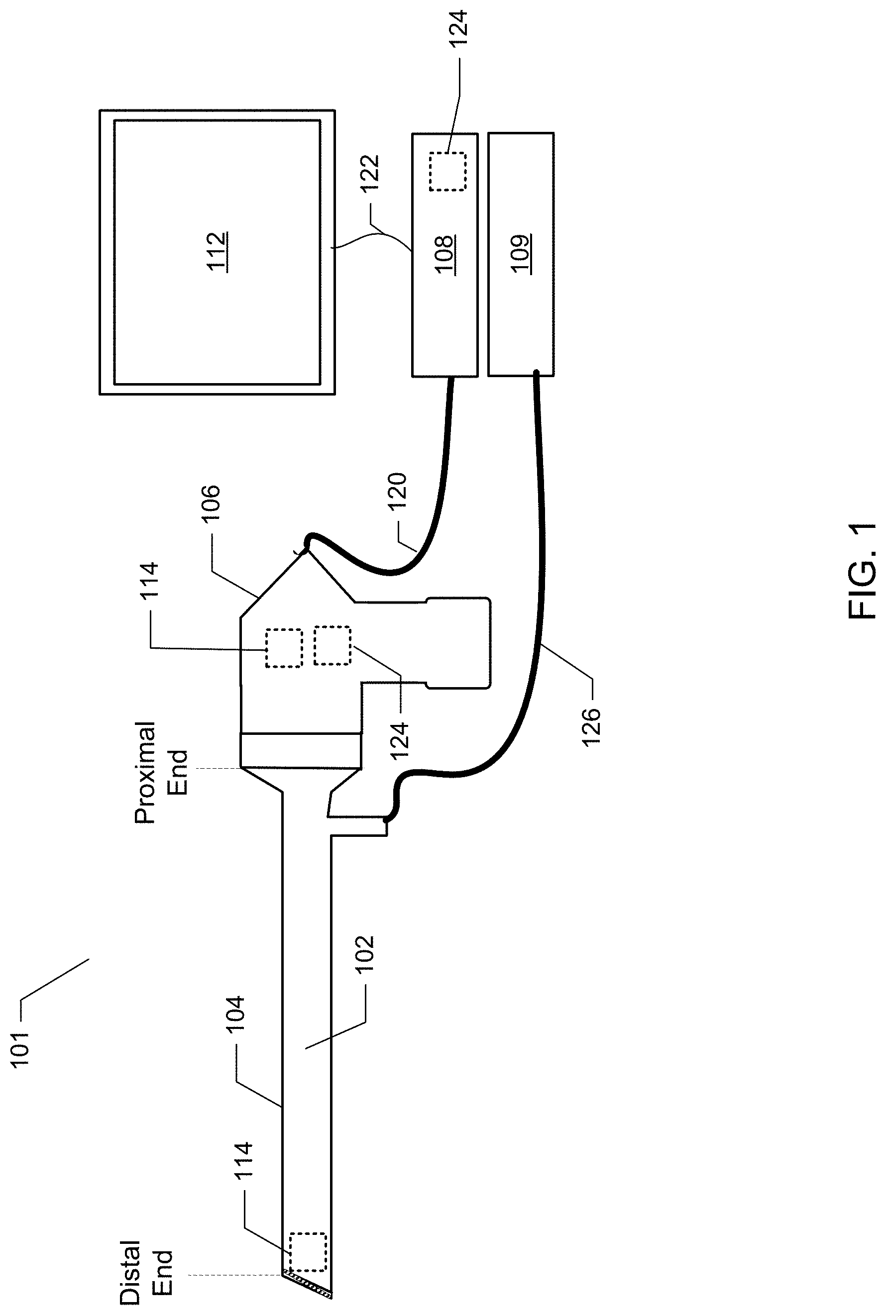
Referring now to FIG. 1, there is illustrated a digital imaging system that utilizes minimal pad interconnects in order to reduce the size of the image sensor for use with an endoscopic device within a light deficient environment. The digital imaging system 101 illustrated in FIG. 1 may comprise an endoscopic device 102 for use in ambient light deficient environment. The endoscopic device 102, in turn, may include an endoscope 104, an endoscope housing 106 (e.g., hand piece and/or camera head), control unit 108, an electronic communication 120, such as an electronic cable, light source 109, a light cable 126, such as a fiber optic cable, connected to light source 109 and endoscopic device 102, display 112, and imaging device 114 (e.g., image sensor and related circuitry etc.). Note that in this example, to facilitate discussion, the endoscope device 104, endoscope housing 106, control unit 108, light source 109, display 112, and imaging device 114 are each shown individually with respect to one another. However, it is to be appreciated and understood that this is not to be interpreted as limiting, and any one or more of these components can be integrated and/or connected in any suitable way.
It will be appreciated that imaging device 114 may include an image sensor comprising a pixel array, wherein a scene is continuously focused onto the pixel array. It will be appreciated that the image sensor senses reflected electromagnetic radiation using or with the pixel array. The pixel array generates image data and an image frame is created from the image data. A processor 124 may detect image textures and edges within the image frame and may further enhance textures and edges within the image frame. The processor 124, whether in the housing 106 or at the control unit 108, may also retrieve from memory properties pertaining to the pixel technology and the applied sensor gain to assess an expectation for the magnitude of noise within an image frame created by said sensor and using said noise expectation to control the edge enhancement application. A stream of images may be created by sequentially combining a plurality of the image frames.
It will be appreciated that traditional rod-lens endoscopes, used for laparoscopy, arthroscopy, urology, gynecology and ENT (ear-nose-throat) procedures, are expensive to manufacture owing to their complex optical composition. The incident image information is transported in the optical domain all the way along its length. Typically it is optically coupled to a hand-piece unit, wherein the image sensing device(s) reside. This type of rigid endoscope is also delicate and prone to damage during handling, use and sterilization. The necessary repair and sterilization processes add further expense to each procedure for which they are utilized.
Advances in imaging technology have led to complementary metal-oxide semiconductor (CMOS) sensors that are cheap to manufacture and are highly customizable. Much of the external circuitry that was necessary to operate charge-coupled device (CCD) based sensors may be integrated into the same chip as the pixel array and lower operation voltages are needed. Therefore CMOS-based cameras are much cheaper and easier to manufacture and may be much more versatile than their CCD-based counterparts. For similar reasons, CMOS sensors are appearing more and more within endoscope systems.
Much cheaper endoscopes may be realized by placing the image sensing device at the distal end, since the optical transport assembly may be effectively replaced by a simple plastic lens stack, not dissimilar to what exists in a typical cell phone camera. They may be so inexpensive in fact that it may make more financial sense to have them be manufactured for single use only, to be subsequently disposed of or recycled, since that negates the repair and sterilization processes.
The difficulty in creating such an endoscope solution is in maintaining image quality since the region into which the sensor must fit is highly space constrained in both dimensions. Reducing the sensor area generally implies a reduction in pixel count and/or pixel area which may impact the resolution, sensitivity and dynamic range. Normally, endoscope systems are geared toward sensing steady broadband illumination and providing color information by segmenting the array into pixels of three or more ranges of wavelength sensitivity. This is done by crafting an individual color filter over each pixel, the Bayer mosaic being the most common solution. One way to avoid resolution loss is to eliminate the color filters since with the Bayer mosaic e.g. there may be up to a factor 1/ 2 loss in luminance resolution (in x or y) as compared with the native array resolution. The color information in such a case can be provided by pulsing a laser or LED-based illuminants with different wavelengths or combinations thereof during separate frame captures. Applicant has developed such systems and devices, which allow for high definition quality at progressive frame rates of 60 Hz or higher by virtue of a special sensor design. Additional developments by Applicant allow for the peripheral circuitry to be reduced to its minimal area while transmitting image data off chip in the digital domain.
It will be appreciated by those of skill in the art that each bond pad occupies significant physical space on a chip. Each bond pad is used to provide power or input/output signals to and from the sensor chip. Therefore in striving for minimal area it is desirable to reduce the number of bond pads as much as possible. This disclosure described a strategy for reducing pad count by combining digital input and output functionality into the same bi-directional pads. During image transmission they act as differential outputs. Then during a defined portion of each frame, they switch direction, in order to enable commands to be received. This requires that the camera control electronics have the commands issued to the sensor synchronized to the timing of the frame. This approach may be useful in the context of many CMOS sensor applications since sensor cost scales with chip area.
Another way to reduce the pad count described herein, is to use only a single external power supply and use, e.g., internal DC to DC converters or regulators to provide for multiple internal (e.g., analog and digital) supplies.
Further to this, in the context of an endoscope system, the simplicity and manufacturability can be enhanced by customizing the image sensor in order to receive commands and information from the endo scope hand-piece. The information may then be subsequently incorporated into the output data issued by the sensor. This reduces the overall conductor count from endoscope to camera system. Such information sources may include user instigated button events or measurements of the angle of rotation of the endoscope with respect to the hand-piece. Angular measurements are necessitated by certain embodiments of endoscopes having their image sensors placed at the distal end.
CMOS image sensors typically incorporate two different power supplies, necessitating three pads: VDD1, VDD2 & GND. The higher of the two voltages is used predominantly for the purpose of biasing the pixel array. Occasionally it will also be used to power input/output circuits. The lower voltage would typically be used to power the peripheral analog circuitry and the digital portion of the sensor, where applicable. Sometimes however, certain analog readout elements are powered using the higher supply voltage, which is usually in the range of about 3V to about 4V.
One strategy for reducing the pad count is to supply only a single power level and have the second one derived on-chip. This would also be effective in removing a power circuit (regulator etc.) from the camera system.
FIG. 2 illustrates one implementation of an internal up-conversion from a supplied low voltage to the higher voltage. This example is based upon a switch-cap DC-DC up-convertor 200. Both the flying cap (C1) and the decoupling cap (C2) are internal. The low power voltage (low VDD) supplies the up-convertor along with the relevant internal circuitry. It will be appreciated that an oscillator (not illustrated in FIG. 2) delivers the correct switching pattern to S1 through S4. This oscillator may be powered from the low voltage and proper level shifting needs to happen to have the correct switching voltage levels. The generated power supply may be tuned by carefully choosing the oscillator frequency, the internal resistance of the switch and the ratio between the flying cap and the decoupling cap (C1/C2).
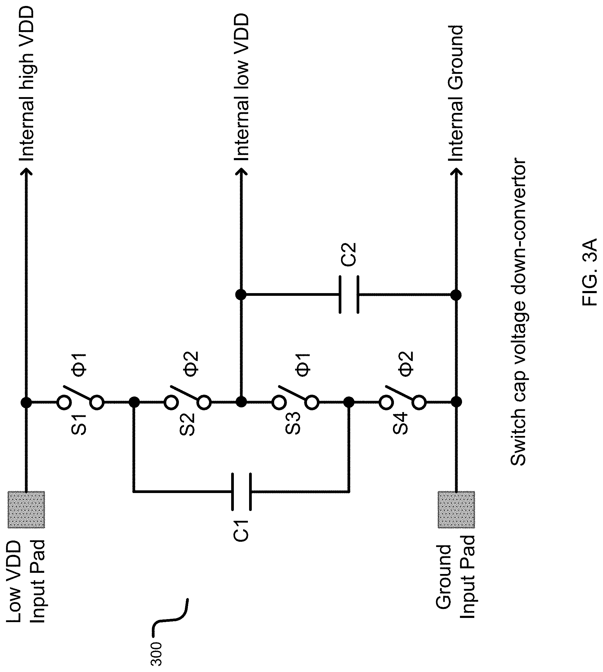
In another implementation, the supplied voltage may be the high voltage supply (high VDD). FIGS. 3A and 3B depict two examples of a down regulator that may be used in this configuration. FIG. 3A illustrates a system that is based upon a switch-cap DC-DC down-convertor 300. It should be noted that in an implementation, similar considerations may be applied as for the convertor in FIG. 2.
FIG. 3B illustrates an implementation comprising a Low Drop Out regulator (LDO) 302 is based upon a linear circuit. The internal reference may come from a simple resistive divider or from a band gap reference generator. Although less susceptible to pick-up noise (as there are no switching elements), the LDO is often less efficient than its switch-cap counterpart.
It should be noted that in general, up-conversion may be used more readily than down regulators. This is because the sensor high voltage is usually less critical in terms of noise and requires less current consumption. Therefore the specifications for an up-converter are less demanding.
The CMOS image sensors of the disclosure may have a plurality of internal on-chip registers. These provide the sensor with flexibility and optimization options. The presence of these registers usually necessitates dedicated digital pads, in order that they may be configured using a defined slow-control protocol.
A system and method for eliminating or reducing these digital pads, while maintaining configurable registers may comprise the following. The system and method may be based on an approach that uses dual purpose pads for both input and output. These pads are designed to automatically switch between the output and input states at well-defined times. When the pads are acting as outputs, image data and other types of data are issued from the sensor. When the pads are in the input state they may receive slow control commands. To facilitate this, the frame period may be divided into three defined states, rolling-readout (image data is issued), service-lines (other types of data issued) and the configuration phase, during which the pads become inputs. The camera system needs to know what state the sensor pads are in at all times. During the rolling-readout and service-line phases, the camera system may not issue slow-control commands.
FIG. 4 Illustrates an implementation of a method of timing. The frame timing structure 400 is depicted in FIG. 4 wherein the configuration and service-line phases are also used to pulse the light in pulsed illumination-based systems.
For reasons of cost, simplicity and manufacturability, it may be advantageous to conceive of an endoscope with a minimal number of conductors, with no active components other than the sensor, and a cable that solely incorporates the communication protocol between the sensor and the remainder of the camera system. When combined with bi-directional sensor data pads 405 and internal voltage generation (as per the methods described herein), the cable may be as minimal as having just as many data wires as needed to support the requisite image bandwidth and one power supply requiring just two wires (i.e., power and ground).
In a conventional modern endoscope, dedicated electrical connections may be needed for operations that are not directly related to the sensor. For example there are extra wires to service hand-piece buttons. These may be wires connected directly to the button, or alternatively to a local microcontroller that also serves also other functions.
In other examples, sensors may be needed to determine the angular position of the endoscope. The angle information should be relayed using various methods and structures to the image processing chain (ISP) within the camera system.
One strategy for reducing the endoscope conductor count is that any low speed analog and digital signals, instead of being sent directly to the camera system, may be re-routed to the CMOS image sensor. Within the sensor the signals may be digitally converted, if necessary, before being encoded alongside the image data or in lieu of pixel data within special service lines. Such as a strategy may eliminate the need for extra wires in the endoscope cable and extra active components within the endoscope hand-piece or lumen. Issuing the data at the sensor frame rate may also allow for increased (i.e., faster) system response. The camera system simply needs to decode this "hidden" information and act accordingly.
FIG. 5 illustrates an implementation of connections between the endoscope buttons 505 and the sensor 555 based upon a resistance network. In this approach, a series of on-chip comparators 510 may convert the analog signal into a digital word ready to be issued as output data.
FIG. 6 illustrates an implementation in which an angular position Hall Effect sensor 622 delivers an analog voltage directly to the CMOS image sensor 655. In this case, the analog voltage may be converted by an on-chip analog-digital converter (ADC) and inserted within the frame.
FIG. 7 illustrates two possible encoding examples for digital data words within the frame data. They may be, for example, inserted in the row header 705 or by replacing "pixel" data within the service rows 710. It should be noted that there are multiple other configurations for encoding digital data words within the CMOS sensor image data and all such configurations are intended to fall within the scope of this disclosure.
It should also be noted that FIG. 5 and FIG. 6 are merely exemplary and other forms of data may be sent to the CMOS sensor other than that described above without departing from the scope of the disclosure. Such data comprises digital data for which case a serial communication protocol would serve the purpose well.
Implementations of the disclosure may comprise or utilize a special purpose or general-purpose computer including computer hardware, such as, for example, one or more processors and system memory, as discussed in greater detail below. Implementations within the scope of the disclosure may also include physical and other computer-readable media for carrying or storing computer-executable instructions and/or data structures. Such computer-readable media can be any available media that can be accessed by a general purpose or special purpose computer system. Computer-readable media that store computer-executable instructions are computer storage media (devices). Computer-readable media that carry computer-executable instructions are transmission media. Thus, by way of example, and not limitation, implementations of the disclosure can comprise at least two distinctly different kinds of computer-readable media: computer storage media (devices) and transmission media.
Computer storage media (devices) includes RAM, ROM, EEPROM, CD-ROM, solid state drives ("SSDs") (e.g., based on RAM), Flash memory, phase-change memory ("PCM"), other types of memory, other optical disk storage, magnetic disk storage or other magnetic storage devices, or any other medium which can be used to store desired program code means in the form of computer-executable instructions or data structures and which can be accessed by a general purpose or special purpose computer.
A "network" is defined as one or more data links that enable the transport of electronic data between computer systems and/or modules and/or other electronic devices. In an implementation, a sensor and camera control unit may be networked in order to communicate with each other, and other components, connected over the network to which they are connected. When information is transferred or provided over a network or another communications connection (either hardwired, wireless, or a combination of hardwired or wireless) to a computer, the computer properly views the connection as a transmission medium. Transmissions media can include a network and/or data links which can be used to carry desired program code means in the form of computer-executable instructions or data structures and which can be accessed by a general purpose or special purpose computer. Combinations of the above should also be included within the scope of computer-readable media.
As can be seen in FIG. 8, various computer system components, program code means in the form of computer-executable instructions or data structures that can be transferred automatically from transmission media to computer storage media (devices) (or vice versa). For example, computer-executable instructions or data structures received over a network or data link can be buffered in RAM within a network interface module (e.g., a "NIC"), and then eventually transferred to computer system RAM and/or to less volatile computer storage media (devices) at a computer system. RAM can also include solid state drives (SSDs or PCIx based real time memory tiered Storage, such as FusionIO). Thus, it should be understood that computer storage media (devices) can be included in computer system components that also (or even primarily) utilize transmission media.
Computer-executable instructions comprise, for example, instructions and data which, when executed at a processor, cause a general purpose computer, special purpose computer, or special purpose processing device to perform a certain function or group of functions. The computer executable instructions may be, for example, binaries, intermediate format instructions such as assembly language, or even source code. Although the subject matter has been described in language specific to structural features and/or methodological acts, it is to be understood that the subject matter defined in the appended claims is not necessarily limited to the described features or acts described above. Rather, the described features and acts are disclosed as example forms of implementing the claims.
Those skilled in the art will appreciate that the disclosure may be practiced in network computing environments with many types of computer system configurations, including, personal computers, desktop computers, laptop computers, message processors, control units, camera control units, hand-held devices, hand pieces, multi-processor systems, microprocessor-based or programmable consumer electronics, network PCs, minicomputers, mainframe computers, mobile telephones, PDAs, tablets, pagers, routers, switches, various storage devices, and the like. It should be noted that any of the above mentioned computing devices may be provided by or located within a brick and mortar location. The disclosure may also be practiced in distributed system environments where local and remote computer systems, which are linked (either by hardwired data links, wireless data links, or by a combination of hardwired and wireless data links) through a network, both perform tasks. In a distributed system environment, program modules may be located in both local and remote memory storage devices.
Further, where appropriate, functions described herein can be performed in one or more of: hardware, software, firmware, digital components, or analog components. For example, one or more application specific integrated circuits (ASICs) or field programmable gate arrays can be programmed to carry out one or more of the systems and procedures described herein. Certain terms are used throughout the following description and Claims to refer to particular system components. As one skilled in the art will appreciate, components may be referred to by different names. This document does not intend to distinguish between components that differ in name, but not function.
FIG. 8 is a block diagram illustrating an example computing device 800. Computing device 800 may be used to perform various procedures, such as those discussed herein. Computing device 800 can function as a server, a client, or any other computing entity. Computing device can perform various monitoring functions as discussed herein, and can execute one or more application programs, such as the application programs described herein. Computing device 800 can be any of a wide variety of computing devices, such as a desktop computer, a notebook computer, a server computer, a handheld computer, camera control unit, tablet computer and the like.
Computing device 800 includes one or more processor(s) 802, one or more memory device(s) 804, one or more interface(s) 806, one or more mass storage device(s) 808, one or more Input/Output (I/O) device(s) 810, and a display device 830 all of which are coupled to a bus 812. Processor(s) 802 include one or more processors or controllers that execute instructions stored in memory device(s) 804 and/or mass storage device(s) 808. Processor(s) 802 may also include various types of computer-readable media, such as cache memory.
Memory device(s) 804 include various computer-readable media, such as volatile memory (e.g., random access memory (RAM) 814) and/or nonvolatile memory (e.g., read-only memory (ROM) 816). Memory device(s) 804 may also include rewritable ROM, such as Flash memory.
Mass storage device(s) 808 include various computer readable media, such as magnetic tapes, magnetic disks, optical disks, solid-state memory (e.g., Flash memory), and so forth. As shown in FIG. 8, a particular mass storage device is a hard disk drive 824. Various drives may also be included in mass storage device(s) 808 to enable reading from and/or writing to the various computer readable media. Mass storage device(s) 808 include removable media 826 and/or non-removable media.
I/O device(s) 810 include various devices that allow data and/or other information to be input to or retrieved from computing device 800. Example I/O device(s) 810 include digital imaging devices, electromagnetic sensors and emitters, cursor control devices, keyboards, keypads, microphones, monitors or other display devices, speakers, printers, network interface cards, modems, lenses, CCDs or other image capture devices, and the like.
Display device 830 includes any type of device capable of displaying information to one or more users of computing device 800. Examples of display device 830 include a monitor, display terminal, video projection device, and the like.
Interface(s) 806 include various interfaces that allow computing device 800 to interact with other systems, devices, or computing environments. Example interface(s) 806 may include any number of different network interfaces 820, such as interfaces to local area networks (LANs), wide area networks (WANs), wireless networks, and the Internet. Other interface(s) include user interface 818 and peripheral device interface 822. The interface(s) 806 may also include one or more user interface elements 818. The interface(s) 806 may also include one or more peripheral interfaces such as interfaces for printers, pointing devices (mice, track pad, etc.), keyboards, and the like.
Bus 812 allows processor(s) 802, memory device(s) 804, interface(s) 806, mass storage device(s) 808, and I/O device(s) 810 to communicate with one another, as well as other devices or components coupled to bus 812. Bus 812 represents one or more of several types of bus structures, such as a system bus, PCI bus, IEEE 1394 bus, USB bus, and so forth.
For purposes of illustration, programs and other executable program components are shown herein as discrete blocks, although it is understood that such programs and components may reside at various times in different storage components of computing device 800, and are executed by processor(s) 802. Alternatively, the systems and procedures described herein can be implemented in hardware, or a combination of hardware, software, and/or firmware. For example, one or more application specific integrated circuits (ASICs) can be programmed to carry out one or more of the systems and procedures described herein.
It will be appreciated that the disclosure may be used with any image sensor, whether a CMOS image sensor or CCD image sensor, without departing from the scope of the disclosure. Further, the image sensor may be located in any location within the overall system, including, but not limited to, the tip of the endoscope, the hand piece of the imaging device or camera, the control unit, or any other location within the system without departing from the scope of the disclosure.
Implementations of an image sensor that may be utilized by the disclosure include, but are not limited to, the following, which are merely examples of various types of sensors that may be utilized by the disclosure.
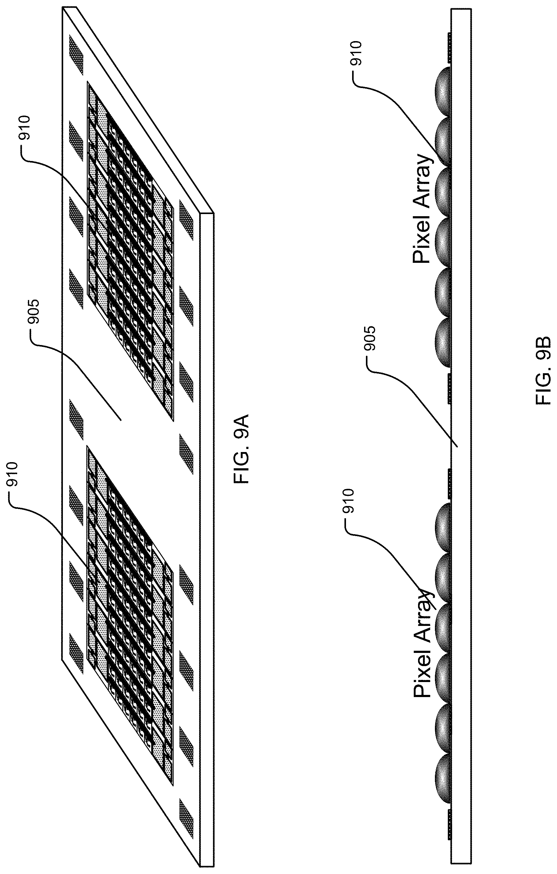
FIGS. 9A and 9B illustrate an implementation of a monolithic sensor 905 having a plurality of pixel arrays 910 for producing a three dimensional image in accordance with the teachings and principles of the disclosure. Such an implementation may be desirable for three dimensional image capture, wherein the two pixel arrays 910 may be offset during use. In another implementation, a first pixel array 910 and a second pixel array 910 may be dedicated to receiving a predetermined range of wave lengths of electromagnetic radiation, wherein the first pixel array 910 is dedicated to a different range of wave length electromagnetic radiation than the second pixel array 910.
FIGS. 10A and 10B illustrate a perspective view of an implementation of an imaging sensor built on a plurality of substrates 1010, 1011. As illustrated, a plurality of pixel columns forming the pixel array 1015 are located on the first substrate 1011 and a plurality of circuit columns 1020 are located on a second substrate 1010. Also illustrated in the figure are the electrical connection and communication between one column of pixels to its associated or corresponding column of circuitry.
In one implementation, an image sensor, which might otherwise be manufactured with its pixel array and supporting circuitry on a single, monolithic substrate/chip, may have the pixel array separated from all or a majority of the supporting circuitry. The disclosure may use at least two substrates/chips, which will be stacked together using three-dimensional stacking technology. The first of the two substrates/chips may be processed using an image CMOS process. The first substrate/chip may be comprised either of a pixel array exclusively or a pixel array surrounded by limited circuitry. The second or subsequent substrate/chip may be processed using any process, and does not have to be from an image CMOS process. The second substrate/chip may be, but is not limited to, a highly dense digital process in order to integrate a variety and number of functions in a very limited space or area on the substrate/chip, or a mixed-mode or analog process in order to integrate for example precise analog functions, or a RF process in order to implement wireless capability, or MEMS (Micro-Electro-Mechanical Systems) in order to integrate MEMS devices. The image CMOS substrate/chip may be stacked with the second or subsequent substrate/chip using any three-dimensional technique. The second substrate/chip may support most, or a majority, of the circuitry that would have otherwise been implemented in the first image CMOS chip (if implemented on a monolithic substrate/chip) as peripheral circuits and therefore have increased the overall system area while keeping the pixel array size constant and optimized to the fullest extent possible. The electrical connection between the two substrates/chips may be done through interconnects, which may be wirebonds, bump and/or TSV (Through Silicon Via).
FIGS. 11A and 11B illustrate a perspective view of an implementation of an imaging sensor having a plurality of pixel arrays for producing a three dimensional image. The three dimensional image sensor may be built on a plurality of substrates 1111a, 1111b, 1111c, and may comprise the plurality of pixel arrays 1115a, 1115b and other associated circuitry 1130a, 1130b, wherein a plurality of pixel columns forming the first pixel array and a plurality of pixel columns forming a second pixel array are located on respective substrates and a plurality of circuit columns are located on a separate substrate. Also illustrated are the electrical connections and communications between columns of pixels to associated or corresponding column of circuitry.
It will be appreciated that the teachings and principles of the disclosure may be used in a reusable device platform, a limited use device platform, a re-posable use device platform, or a single-use/disposable device platform without departing from the scope of the disclosure. It will be appreciated that in a re-usable device platform an end-user is responsible for cleaning and sterilization of the device. In a limited use device platform the device can be used for some specified amount of times before becoming inoperable. Typical new device is delivered sterile with additional uses requiring the end-user to clean and sterilize before additional uses. In a re-posable use device platform a third-party may reprocess the device (e.g., cleans, packages and sterilizes) a single-use device for additional uses at a lower cost than a new unit. In a single-use/disposable device platform a device is provided sterile to the operating room and used only once before being disposed of.
Additionally, the teachings and principles of the disclosure may include any and all wavelengths of electromagnetic energy, including the visible and non-visible spectrums, such as infrared (IR), ultraviolet (UV), and X-ray.
It will be appreciated that various features disclosed herein provide significant advantages and advancements in the art. The following embodiments are exemplary of some of those features.
In the foregoing Detailed Description of the Disclosure, various features of the disclosure are grouped together in a single embodiment for the purpose of streamlining the disclosure. This method of disclosure is not to be interpreted as reflecting an intention that the claimed disclosure requires more features than are expressly recited in each claim. Rather, inventive aspects lie in less than all features of a single foregoing disclosed embodiment.
It is to be understood that the above-described arrangements are only illustrative of the application of the principles of the disclosure. Numerous modifications and alternative arrangements may be devised by those skilled in the art without departing from the spirit and scope of the disclosure and the appended claims are intended to cover such modifications and arrangements.
Thus, while the disclosure has been shown in the drawings and described above with particularity and detail, it will be apparent to those of ordinary skill in the art that numerous modifications, including, but not limited to, variations in size, materials, shape, form, function and manner of operation, assembly and use may be made without departing from the principles and concepts set forth herein.
Further, where appropriate, functions described herein can be performed in one or more of: hardware, software, firmware, digital components, or analog components. For example, one or more application specific integrated circuits (ASICs) can be programmed to carry out one or more of the systems and procedures described herein. Certain terms are used throughout the following description and Claims to refer to particular system components. As one skilled in the art will appreciate, components may be referred to by different names. This document does not intend to distinguish between components that differ in name, but not function.
* * * * *
D00000
D00001
D00002
D00003
D00004
D00005
D00006
D00007
D00008
D00009
D00010
D00011
D00012

XML
uspto.report is an independent third-party trademark research tool that is not affiliated, endorsed, or sponsored by the United States Patent and Trademark Office (USPTO) or any other governmental organization. The information provided by uspto.report is based on publicly available data at the time of writing and is intended for informational purposes only.
While we strive to provide accurate and up-to-date information, we do not guarantee the accuracy, completeness, reliability, or suitability of the information displayed on this site. The use of this site is at your own risk. Any reliance you place on such information is therefore strictly at your own risk.
All official trademark data, including owner information, should be verified by visiting the official USPTO website at www.uspto.gov. This site is not intended to replace professional legal advice and should not be used as a substitute for consulting with a legal professional who is knowledgeable about trademark law.