Precision capacitor
Fernandes , et al. March 30, 2
U.S. patent number 10,964,778 [Application Number 15/902,764] was granted by the patent office on 2021-03-30 for precision capacitor. This patent grant is currently assigned to Texas Instruments Incorporated. The grantee listed for this patent is Texas Instruments Incorporated. Invention is credited to Haowen Bu, Luigi Colombo, Poornika Fernandes.


| United States Patent | 10,964,778 |
| Fernandes , et al. | March 30, 2021 |
Precision capacitor
Abstract
In a described example, an integrated circuit includes a capacitor first plate; a dielectric stack over the capacitor first plate comprising silicon nitride and silicon dioxide with a capacitance quadratic voltage coefficient less than 0.5 ppm/V.sup.2; and a capacitor second plate over the dielectric stack.
| Inventors: | Fernandes; Poornika (Murphy, TX), Colombo; Luigi (Dallas, TX), Bu; Haowen (Plano, TX) | ||||||||||
|---|---|---|---|---|---|---|---|---|---|---|---|
| Applicant: |
|
||||||||||
| Assignee: | Texas Instruments Incorporated
(Dallas, TX) |
||||||||||
| Family ID: | 1000005456231 | ||||||||||
| Appl. No.: | 15/902,764 | ||||||||||
| Filed: | February 22, 2018 |
Prior Publication Data
| Document Identifier | Publication Date | |
|---|---|---|
| US 20190259826 A1 | Aug 22, 2019 | |
| Current U.S. Class: | 1/1 |
| Current CPC Class: | H01G 4/085 (20130101); H01L 28/40 (20130101); H01L 21/0217 (20130101); H01L 29/0649 (20130101); H01L 21/022 (20130101); H01L 27/0629 (20130101); H01L 21/02274 (20130101); H01L 21/02164 (20130101); H01L 21/02211 (20130101) |
| Current International Class: | H01L 49/02 (20060101); H01L 21/02 (20060101); H01L 27/06 (20060101); H01G 4/08 (20060101); H01L 29/06 (20060101) |
| Field of Search: | ;257/532,438 |
References Cited [Referenced By]
U.S. Patent Documents
| 5397748 | March 1995 | Watanabe |
| 6680521 | January 2004 | Kar-Roy et al. |
| 7041569 | May 2006 | Kar-Roy et al. |
| 2013/0157466 | June 2013 | Fox |
| 2015/0214150 | July 2015 | Chang |
| 2016/0104621 | April 2016 | Zang |
| 2016/0163782 | June 2016 | Campbell et al. |
Attorney, Agent or Firm: Keagy; Rose Alyssa Brill; Charles A. Cimino; Frank D.
Claims
What is claimed is:
1. A method for forming an integrated circuit with an embedded capacitor, comprising: forming a capacitor first plate over a semiconductor substrate; and depositing over the capacitor first plate a dielectric stack comprised of alternating layers of plasma enhanced chemical vapor deposition (PECVD) silicon dioxide and PECVD silicon nitride; wherein depositing the PECVD silicon nitride comprises depositing silicon nitride with an atomic hydrogen content less than 25% using N.sub.2 as a nitrogen source while applying radio frequency low frequency (RF-LF) power.
2. The method of claim 1, wherein depositing the dielectric stack further comprises: PECVD depositing a first layer of silicon dioxide, a layer of silicon nitride, and a second layer of silicon dioxide wherein a thickness of the silicon dioxide layers is about half a thickness of the silicon nitride layer; and while depositing the silicon nitride layer, flowing NH.sub.3 and N.sub.2 gasses with a flow ratio of 1:15 or less.
3. The method of claim 2, wherein depositing the PECVD silicon nitride includes depositing while applying an RF-LF power in a range of 80 W to 200 W, while using a N.sub.2 flow rate in a range of 3000 sccm to 10000 sccm, while using a NH.sub.3 flow rate in a range of 0 sccm to 300 sccm.
4. The method of claim 2, wherein depositing the PECVD silicon nitride includes depositing silicon nitride while applying a RF-LF power of about 100 W at 400 kHz, while using an N.sub.2 flow rate of about 4500 sccm, and while using an NH.sub.3 flow rate of about 300 sccm.
5. The method of claim 1, wherein the dielectric stack is a silicon dioxide, silicon nitride, silicon dioxide stack having a thickness of silicon dioxide layers that is about half a thickness of a silicon nitride layer, and wherein the silicon nitride is PECVD deposited with a RF-LF power in a range of 80 W to 200 W, while using a N.sub.2 flow rate in a range of 3000 sccm to 10000 sccm, and while using a NH.sub.3 flow rate of less than 10 sccm.
6. The method of claim 1, wherein the dielectric stack comprises a first silicon dioxide layer with a first thickness, a second silicon nitride layer with a second thickness, and a third silicon dioxide layer with a third thickness, and wherein the first thickness and the third thickness are about equal and wherein the second thickness is about double the first and third thickness, and the PECVD silicon nitride is PECVD deposited with an RF-LF power of about 100 W at 400 kHz, a N.sub.2 flow rate of about 4500 sccm, and an NH.sub.3 flow rate of about 0 sccm.
7. The method of claim 1, wherein the dielectric stack comprises a first silicon nitride layer with a first thickness, a second silicon dioxide layer with a second thickness, and a third silicon nitride layer with a third thickness and the first, second, and third thicknesses are about equal; and wherein the PECVD silicon nitride is PECVD deposited while applying an RF-LF power in a range of 80 W to 200 W, with an N.sub.2 flow rate in a range of 3000 sccm to 10000 sccm, and a NH.sub.3 flow rate is 0 sccm.
8. The method of claim 1, wherein the dielectric stack comprises a first silicon nitride layer with a first thickness, a second silicon dioxide layer with a second thickness, and a third silicon nitride layer with a third thickness and the first, second, and third thicknesses are about equal, and wherein the PECVD silicon nitride is PECV deposited while applying an RF-LF power of about 100 W, with an N.sub.2 flow rate of about 4500 sccm, and an NH.sub.3 flow rate of 0 sccm.
9. A method for forming an integrated circuit with an embedded capacitor, comprising: forming a capacitor first plate on a dielectric layer over a semiconductor substrate; and depositing over the capacitor first plate a dielectric stack comprising a first layer of plasma excited chemical vapor deposition (PECVD) silicon dioxide with a first thickness, a first layer of PECVD silicon nitride with a second thickness, and a second layer of silicon dioxide with the first thickness that is about half the second thickness; wherein depositing the PECVD silicon nitride includes performing deposition while applying N.sub.2 and NH.sub.3 gasses with a flow rate ratio of an NH.sub.3 flow rate to an N.sub.2 flow rate of 1:15 or less, and while applying a radio frequency low frequency (RF-LF) power.
10. The method of claim 9, wherein the PECVD silicon nitride is deposited with an RF-LF power in a range of 80 W to 200 W, an N.sub.2 flow rate in a range of 3000 sccm to 10000 sccm, and an NH.sub.3 flow rate in a range of 0 sccm to 300 sccm.
11. The method of claim 9, wherein the PECVD silicon nitride is deposited with an RF-LF power of about 100 W at 400 kHz, an N.sub.2 flow rate of about 4500 sccm, and an NH.sub.3 flow rate of about 300 sccm.
Description
CROSS-REFERENCE TO RELATED APPLICATIONS
The following related co-owned and co-pending patent application is hereby incorporated by reference in its entirety herein: U.S. patent application Ser. No. 15/902,829, filed contemporaneously.
TECHNICAL FIELD
This disclosure relates generally to integrated circuits, and more particularly to integrated circuits with high voltage and high precision capacitors.
BACKGROUND
A capacitor is an electrical device found in many integrated circuits and is used to store electrical charge and in some applications, to measure electrical charge. Precision capacitors are used to convert analog signals to digital voltage values. Improvements in embedded precision capacitors are needed.
SUMMARY
In a described example, an integrated circuit includes an embedded precision capacitor with a dielectric stack of silicon dioxide and silicon nitride having a capacitance quadratic voltage coefficient of less than 0.5 ppm/V.sup.2. A method for forming an integrated circuit with an embedded capacitor includes: forming a capacitor first plate over a substrate; and depositing over the capacitor first plate a dielectric stack of alternating layers of plasma enhanced chemical vapor deposition (PECVD) silicon dioxide and PECVD silicon nitride, where the silicon nitride has an atomic hydrogen content less than 25% and the silicon nitride is deposited using N.sub.2 as a nitrogen source while applying radio frequency low frequency power.
BRIEF DESCRIPTION OF THE DRAWINGS
FIG. 1 is a cross section of an integrated circuit with an embedded capacitor.
FIG. 2 is a plan view of an integrated circuit with an embedded high precision analog to digital capacitor array.
FIG. 3 is a cross section of an integrated circuit with an embedded capacitor that includes a stacked NON dielectric sandwiched between first and second capacitor plates.
FIG. 4 is a cross section of an integrated circuit with an embedded capacitor that includes a stacked ONO dielectric sandwiched between first and second capacitor plates.
FIG. 5 is a flow diagram of a method for forming an integrated circuit with an embedded capacitor that includes a stacked ONO dielectric with a quadratic voltage coefficient less than 0.5 ppm/V.sup.2.
DETAILED DESCRIPTION
Corresponding numerals and symbols in the different figures generally refer to corresponding parts unless otherwise indicated. The figures are not necessarily drawn to scale.
The term "RF-LF" is used herein as an abbreviation for "radio frequency low frequency". An RF-LF signal is sometimes applied during dielectric depositions in processes using plasma enhanced chemical vapor deposition in the range of 0-500 kHz. The term "RF-HF" is used herein to abbreviate the term "radio frequency high frequency". An RF-HF signal applied during dielectric depositions PECVD is in the range of 10-20 MHz and is often 13.56 MHz, a selected frequency that is available for industrial applications without interfering with other radio frequency signals.
FIG. 1 illustrates a capacitor structure 100 in a cross section. The capacitor structure 100 includes a capacitor dielectric 108 between a capacitor second plate 112 and a capacitor first plate 104. The capacitor dielectric 108 is a dielectric such as silicon dioxide, silicon nitride, silicon oxynitride, or a dielectric stack with several silicon dioxide and silicon nitride layers. The second and first capacitor plates, 112 and 104, are conductive materials, such as: doped polysilicon; a silicide, such as titanium silicide, cobalt silicide, nickel silicide, molybdenum silicide, and platinum silicide; or a metallic material, such as an aluminum and aluminum alloys, copper and copper alloys, tungsten, titanium-tungsten, tantalum nitride, and titanium nitride and alloys of these metallic materials.
In FIG. 1, the capacitor structure 100 is built on a non-conducting substrate 102. The non-conducting substrate can be a dielectric layer overlying a conductive substrate, an integrated circuit, or an isolation area such as shallow trench isolation (STI) within an integrated circuit. Electrical contact is made to the capacitor first plate 104 with a first metal filled contact or via 118 and electrical contact is made to the capacitor second plate 112 with a second metal filled contact or via 116.
The amount of charge, Q, that can be stored on a capacitor is given by Equation 1: Q=CV (1) Where: Q is charge in units of femtofarads (fF), C is the capacitance in units of femtofarads per volt (fF/V), and V is the voltage in units of volts applied to the capacitor plates across the capacitor dielectric (108 in FIG. 1).
The amount of charge that can be stored on a capacitor in an integrated circuit is limited by the breakdown voltage, V.sub.BD, of the capacitor dielectric 108. A capacitor with a higher V.sub.BD can store more charge.
Integrated circuits (ICs) with analog to digital (A/D) converters (ADCs) use embedded high precision capacitors to accurately measure the electrical charge in an analog voltage signal and convert it to a digital voltage value. FIG. 2 is a plan view for an IC with an A/D converter. The A/D converter IC 220 has peripheral circuitry including transistors 224 and resistors 222 and an array of high precision capacitors 200. When an analog voltage signal is applied by the peripheral circuitry to the high precision capacitor array 200, depending upon the magnitude of the analog voltage signal, a different number of the individual high precision capacitors 220 in the array become fully charged. The number of high precision capacitors 220 that become fully charged is proportional to a digital value corresponding to the voltage.
The precision or number of bits of the digital voltage value is determined by the precision and matching of the high precision capacitors storing the electrical charge. A nonlinear response of capacitance to the analog voltage applied to the capacitor plates limits the precision of A/D conversion.
The voltage dependent capacitance C(V) of a capacitor is given by Equation 2: C(V)=C.sub.O(.alpha.V.sup.2+.beta.V+1) (2) Where: C.sub.O is a capacitance coefficient in units of fF/.mu.m.sup.2 at zero volts; .alpha. is the capacitance quadratic voltage coefficient (CQVC) in units of ppm/V.sup.2; and .beta. is the capacitance linear voltage coefficient (CLVC) in units of ppm/V.
Lower voltage coefficients, .alpha. and .beta., enable conversion of an analog voltage signal to a digital voltage value with higher precision. Precision capacitors can be formed in an integrated circuit using capacitor dielectrics such as silicon dioxide (SiO.sub.2) (referred to as silicon dioxide, oxide, or O), silicon nitride (Si.sub.3N.sub.4) (referred to as SiN, silicon nitride, nitride, or N), and dielectric stacks such as ONO or NON stacks that are deposited using PECVD. In PECVD processes, silane (SiH.sub.4) gas plus a nitrogen source such as ammonia (NH.sub.3) or nitrogen (N.sub.2) gas can be used to deposit PECVD SiN. SiH.sub.4 and an oxygen source such as oxygen (O.sub.2), nitrous oxide, or tetraethyl orthosilicate (TEOS) gas can be used to deposit PECVD SiO.sub.2. Radio frequency high frequency power (RF-HF) is used for plasma excitation of the PECVD reaction, for example, an RF-HF signal at a frequency of 13.56 MHz is used in an existing commonly used PECVD tool.
In one arrangement the breakdown voltage (V.sub.BD) of PECVD SiN is increased by replacing some or all the NH.sub.3 during the PECVD SiN deposition with N.sub.2. In example arrangements, V.sub.BD is further improved by adding radio frequency low frequency (RF-LF) power (400 kHz in an example PECVD tool) to break the N--N bonds in the N.sub.2 gas. The use of RF-LF power increases the number of nitrogen-to-nitrogen (N--N) bonds and increases the number of silicon to nitrogen (Si--N) bonds in the SiN film, and reduces the number of Si--H and N--H bonds. N--N and Si--N bonds are stronger than N--H and Si--H bonds, and increasing the number of these bonds results in an increase in the breakdown voltage V.sub.BD of the SiN film. As is shown in Table 1, when the hydrogen content of the SiN film is reduced from about 28.4 atomic percent in the high hydrogen film to about 13 atomic percent in the low hydrogen-1 film, the breakdown voltage V.sub.BD is raised from about 25.8 V in the high hydrogen film to about 32.4 V in the low hydrogen-1 film.
TABLE-US-00001 TABLE 1 Stacked Capacitor Dielectric Films High Low Low Low Units Hydrogen Hydrogen-1 Hydrogen-2 Hydrogen-4 SiN film NON NON NON ONO capacitance fF/.mu.m.sup.2 1.47 1.61 1.65 1.45 per unit area V.sub.BD Volts 25.8 32.4 30.7 35.1 Target nm 10/10/10 10/10/10 10/10/10 7.5/15/7.5 Thickness TEM nm 25.1 29.7 25.7 na Thickness (9.7/8.6/6.8) (12.3/8.3/9.1) (10.1/7.9/7.7) % Hydrogen Atomic % 28.4 13 -- 22 in SiN layer
TABLE-US-00002 TABLE 2 Stacked Capacitor Dielectric Films Pressure Temp RF-HF RF-LF SiH.sub.4 NH.sub.3 N.sub.2 SiN film (Torr) .degree. C. Watts Watts sccm sccm sccm High Hydrogen 4 400 150 0 18 2150 4500 Low Hydrogen-1 3.5 400 50 100 18 0 4500 Low Hydrogen-2 2.5 400 50 100 25 60 4500 Low Hydrogen-4 2 400 50 100 25 300 4500
Where "sccm" is the standard unit for flow rates, standard cubic centimeters per minute.
FIG. 3 illustrates in a cross section a capacitor 300 with a NON dielectric stack 305. In FIG. 3 similar reference labels are used for similar elements shown in FIG. 1, for clarity. For example, substrate 302 in FIG. 3 corresponds to substrate 102 in FIG. 1. The capacitor 300 includes a NON dielectric stack 305 between a capacitor second plate 312 and a capacitor first plate 304. The capacitor first plate 304 is deposited before capacitor second plate 312. The NON dielectric stack 305 is a SiO.sub.2 layer 308 sandwiched between a first SiN layer 306 and a second SiN layer 310. The target thicknesses of the silicon nitride and silicon dioxide layers in the NON dielectric stack are about equal thicknesses. The total thickness of the example NON stack dielectric in Table 1 is 30 nm (10 nm/10 nm/10 nm). In the example arrangements described hereinbelow, the second capacitor plate, 312, is tantalum nitride, and the first capacitor plate, 304, is cobalt silicide. Other arrangements can utilize other silicides or conductors as a capacitor first plate 304 and other conductors for the capacitor second plate 312. Metals and alloys of the metals can be used.
In Table 1 the breakdown voltage of the high hydrogen SiN film is 25.8 volts whereas the breakdown voltages of the low hydrogen films are 32.4 and 30.7 volts. The higher breakdown voltage enables a higher voltage to be applied to the capacitor in operations of the integrated circuit. This increases the capacitance (see Equation 1) and enables a smaller capacitor to be formed for a given capacitance, reducing the area and cost of the integrated circuit.
The process conditions for the high hydrogen and low hydrogen SiN films listed in Table 1 are given in Table 2. Radio frequency high frequency power (RF-HF) is sufficient to drive the reaction between SiH.sub.4 and NH.sub.3 to form SiN (for example, a frequency of 13.56 MHz can be used in an example PECVD tool). Radio frequency low frequency power (RF-LF) is added to drive the reaction between SiH.sub.4 and N.sub.2 to form SiN (400 kHz in an example PECVD tool). In column 2 of Table 1, the NON dielectric stack with the low hydrogen-1 SiN film has the lowest atomic percent hydrogen (13% H) and the highest breakdown voltage (32 volts). When depositing this SiN film, the NH.sub.3 gas flow is turned off and the nitrogen in the SiN film is supplied from N.sub.2 gas (See row 2 in Table 2).
The above described PECVD films are deposited in an example PECVD deposition tool with RF-HF of 13.56 MHz and with RF-LF of 400 kHz. The arrangements can be adapted by modifying the above PECVD deposition recipes to other recipes, and to recipes compatible with various PECVD deposition tools, to deposit NON, ONO, 0 and N dielectric films with improved V.sub.BD.
A SiN film with high breakdown voltage can be deposited using SiH.sub.4 and N.sub.2 reaction gases and using PECVD with RF-HF power in the range of about 40 Watts to about 100 Watts, with RF-LF power in the range of about 80 Watts to about 200 Watts, temperature in the range of about 300.degree. C. to 500.degree. C., pressure in the range of about 2 Torr to about 5 Torr, with a SiH.sub.4 flow rate between about 15 sccm and 50 sccm, with a N.sub.2 flow rate between about 3000 sccm and 10000 sccm. Sometimes for other SiN film properties it is advantageous to add a small amount of NH.sub.3 gas. A SiN film with improved V.sub.BD can be deposited using the above deposition conditions plus a NH.sub.3 flow rate between about 0 sccm and 300 sccm.
The above arrangement is illustrated using an NON dielectric stacked capacitor. Other arrangements such as an ONO dielectric stacked capacitor can also be used to increase the V.sub.BD. For example, the ONO dielectric stack with the low hydrogen-4 film in Table 1 has a V.sub.BD of 35 V. In alternative arrangements capacitor dielectric stacks with more layers of N and O such as an ONONO or an NONON stack can be used. Dielectric stacks of NON and ONO are preferred because additional ON interfaces can add defects which can adversely affect the V.sub.BD of the capacitor.
High precision capacitors used in analog-to-digital (A/D) integrated circuits can be formed using a dielectric stack such as NON and ONO. N and O dielectric stacks are used, in part, because these dielectric stacks have smaller capacitance nonlinearity than a capacitor dielectric of a single layer of silicon dioxide or silicon nitride. The nonlinearity of silicon nitride films is opposite sign to the nonlinearity of silicon dioxide films so that a dielectric stack with both N and O layers can have a nonlinearity that is less than either the N or O single layer dielectric.
High precision capacitors in ADCs are used to accurately measure the amount of charge in an analog signal and convert it to a digital value. The precision of the digital value (number of bits) is determined by how accurately the precision capacitor measures the charge in the analog signal. One difficulty is that capacitance changes with applied voltage in a nonlinear fashion as given by Equation (2). The quadratic term, .alpha.V.sup.2, determines the nonlinear change in capacitance C(V) with voltage. The magnitude of this term limits the precision of the converted A/D signal. The quadratic response of a capacitor with a NON or ONO dielectric stack can be minimized by optimizing the thicknesses of the N and O films in the dielectric stack. The quadratic response of SiO.sub.2 (O) is opposite to SiN (N) (see Table 3). In an arrangement, after optimizing the thicknesses of the O and N films in the dielectric stack to minimize nonlinearity, the quadratic response of an ONO or NON capacitor dielectric stack can additionally be reduced by lowering the atomic percentage of hydrogen in the SiN layer in the dielectric stack. ONO is the preferred dielectric stack in high precision capacitors and is used below for illustration.
FIG. 4 illustrates in another cross section a capacitor 400 with an ONO dielectric stack 405. In FIG. 4 similar reference labels are used for similar elements shown in FIG. 1, for clarity. For example, substrate 402 in FIG. 4 corresponds to substrate 102 in FIG. 1. The capacitor structure 400 is an ONO dielectric stack 405 sandwiched between a second capacitor plate 412 and a first capacitor plate 404. The ONO dielectric stack 405 is a SiN layer 408 sandwiched between a first SiO.sub.2 layer 406 and a second SiO.sub.2 layer 410. The target thickness of the silicon dioxide/silicon nitride/silicon dioxide (ONO) dielectric stacks in the example dielectric stack in Table 3 is 30 nm (7.5 nm/15 nm/7.5 nm). In this arrangement the thicknesses of the first 408 and second 410 O layers are about half the thickness of the N layer 408. In the arrangements described below the second capacitor plate, 412 is TaN and the first capacitor plate 404 is cobalt silicide. Other arrangements can use other silicides or other metals or alloys as a first capacitor plate 404 and as the second capacitor plate 412.
TABLE-US-00003 TABLE 3 Stacked Capacitor Dielectric Films Units Low H 3 High H High H Low H 3 Low H 4 film Si.sub.3N.sub.4 SiO.sub.2 NON ONO ONO ONO capacitance fF/.mu.m.sup.2 1.61 1.65 1.65 1.38 1.5 1.45 per unit area Breakdown Volts 18.8 26.9 30.5 32.1 33 35.1 Target nm 300 300 10/10/10 7.5/15/7.5 7.5/15/7.5 7.5/15/7.5 Thickness VCLC (.beta.) ppm/V -19.58 -4.20 -4.79 -6.36 -2.38 -2.85 VCQC (.alpha.) ppm/V.sup.2 6.52 -4.89 2.92 0.41 -0.29 -0.08 % Hydrogen Atomic 28.4 na 28.4 28.4 21 22 in SiN layer %
TABLE-US-00004 TABLE 4 Stacked Capacitor Dielectric Films Pressure Temp RF-HF RF-LF SiH.sub.4 NH.sub.3 N.sub.2 SiN film (Torr) .degree. C. Watts Watts sccm sccm sccm High Hydrogen 4 400 150 0 18 2150 4500 Low Hydrogen 3 2 400 50 100 25 180 4500 Low Hydrogen 4 2 400 50 100 25 300 4500
As shown in column 8 in Table 3, the low hydrogen-4 ("Low H 4") film has a capacitance quadratic voltage coefficient, .alpha., of -0.08 ppm/V.sup.2. This .alpha. is smaller than the .alpha. of other ONO dielectric stacks in Table 3. The reduced capacitance nonlinearity with this small .alpha. enables the conversion of an analog signal to a digital signal with a higher number of bits (increased precision).
As shown in row seven of Table 3, labeled "% Hydrogen in SiN layer", the high hydrogen silicon nitride films have a hydrogen content of 28 atomic percent or greater. The low hydrogen silicon nitride films have hydrogen content of 22 atomic percent or less. The hydrogen content of a low hydrogen content silicon nitride film is preferred to be less than about 25 atomic percent for a capacitance quadratic voltage coefficient (CQVC) of less than about +/-0.5 ppm/V.sup.2. It is more preferred for the hydrogen content of the silicon nitride film to be less than about 20 atomic percent.
The PECVD depositions listed in Tables 3 and 4 in this example are performed in an example PECVD deposition tool with radio frequency high frequency (RF-HF) of 13.56 MHz and with radio frequency low frequency (RF-LF) of 400 kHz. Additional arrangements can be formed by adapting the above PECVD deposition recipes to other recipes and to additional recipes compatible with various other PECVD deposition tools to deposit NON and ONO dielectric stacks with improved linearity.
The process conditions for the low hydrogen-4 SiN layer in the ONO dielectric stack are given in row 4 in Table 4. The flow rate of NH.sub.3 is 15 times less than the flow rate of N.sub.2, or even lower. The low NH.sub.3 to N.sub.2 flow ratio in the reaction gas mixture gives rise to the small .alpha. (-0.08 ppm/V.sup.2) (see Equation 2 herein above).
A low hydrogen content SiN film with a small .alpha. may be deposited using N.sub.2, NH.sub.3, and SiH.sub.4 reaction gases and using PECVD with RF-HF power in the range of about 40 Watts to about 100 Watts, with RF-LF power in the range of about 80 Watts to about 200 Watts, temperature in the range of about 300.degree. C. to 500.degree. C., pressure in the range of about 2 Torr to about 5 Torr, with a SiH.sub.4 flow rate between about 15 sccm and 50 sccm, with a N.sub.2 flow rate between about 3000 sccm and 10000 sccm, and with a NH.sub.3 flow rate between about 0 sccm and 300 sccm. Deposition conditions for the example ONO dielectric stack with the low .alpha. listed in Table 3 are given in Table 4.
The O films in the ONO dielectric stack in this example are deposited using the same deposition conditions as the N film with O.sub.2 gas flow turned on, with the NH.sub.3 gas flow turned off and with the RF-LF power turned off. Other deposition conditions and deposition gases can be used to deposit the O films.
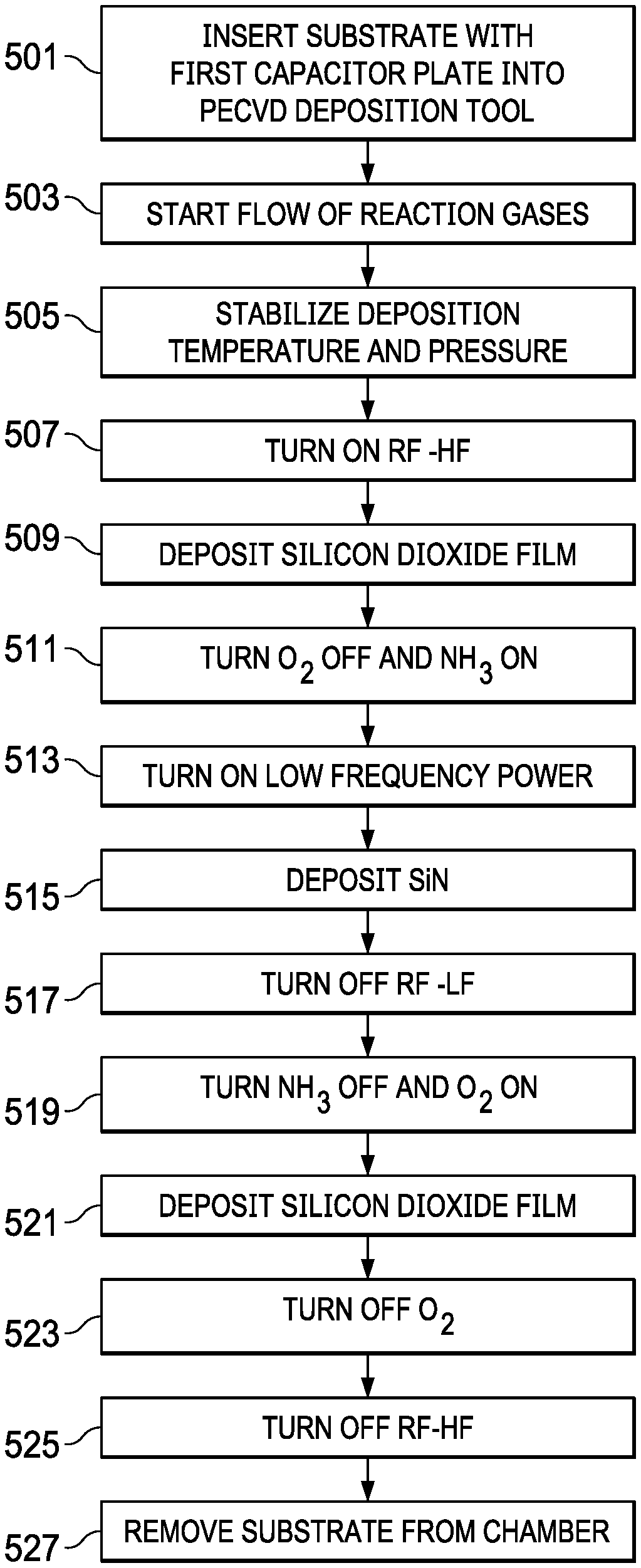
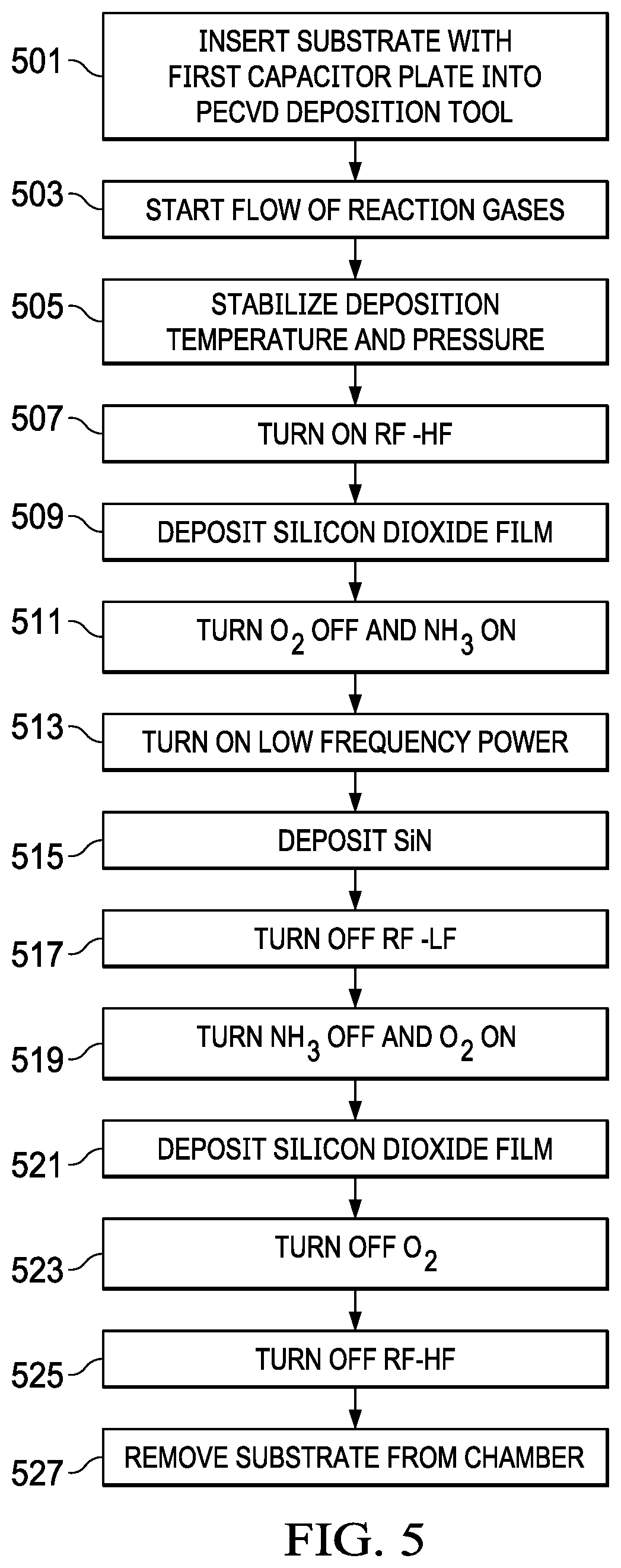
FIG. 5 is a flow diagram a process arrangement for PECVD deposition of an ONO dielectric stack with low nonlinearity. The flow diagram is for an ONO dielectric stack but can readily be adapted for deposition of a NON dielectric stack or for an ON or NO dielectric stack.
In step 501 a substrate such as an integrated circuit wafer with a capacitor first plate formed thereon is loaded into the PECVD tool deposition chamber. The capacitor first plate can be formed on a non-conductive substrate, such as a dielectric layer overlying an integrated circuit or on an isolation dielectric on a substrate. The capacitor first plate can be any conductive material, such as doped single crystal silicon, doped polysilicon, silicides, metals and alloys. In the arrangements for the examples shown in Tables 1 and 3, the first plate is cobalt silicide formed on doped polysilicon.
In step 503 the reaction gases start flowing into the deposition chamber. In this arrangement the deposition gasses for the SiO.sub.2 layer are SiH.sub.4 and N.sub.2O with N.sub.2 carrier gas. Other gases such as SiH.sub.2Cl.sub.2, Si.sub.2H.sub.6, to provide the silicon atoms and other gases such as O.sub.2, NO and TEOS to provide the oxygen atoms can also be used with appropriate changes to the deposition conditions to deposit the SiO.sub.2 layer.
In step 505 the deposition temperature and pressure are stabilized. In an example deposition, the temperature is stabilized at about 400.degree. C. and the pressure is stabilized at about 2 Torr.
In step 507 the RF-HF power is turned on. In an example the RF-HF power is about 50 W at 13.56 MHz.
In step 509 the first SiO.sub.2 layer of the ONO dielectric stack is deposited onto the capacitor first plate.
In step 511, after the desired thickness of the first SiO.sub.2 layer is deposited, the flow of the N.sub.2O gas is stopped and the flow of the NH.sub.3 gas is started. Turning off the flow of the N.sub.2O gas stops the deposition of the first SiO.sub.2 dielectric layer. As shown in Table 4, a high flow rate of N.sub.2 gas (4500 sccm) along with a low flow rate of NH.sub.3 gas (300 sccm or less) is used to deposit a silicon nitride film with low hydrogen content (less than 25 atomic percent hydrogen). The ratio of the flow rate of NH.sub.3 to N.sub.2 is preferred to be 1:15 or less. For some applications such as those that may benefit from a higher V.sub.BD, the NH.sub.3 flow rate may be turned off.
In step 513 the RF-LF power is turned on. This initiates the reaction between SiH.sub.4 and N.sub.2 to deposit the low hydrogen SiN layer in the ONO dielectric stack. In one example the RF-LF power is about 100 W at 400 kHz.
In step 515 the desired thickness of the SiN layer is deposited.
In step 517 the RF-LF power is turned off. This stops the SiN layer deposition from the reaction of SiH.sub.4 and N.sub.2.
In step 519 the NH.sub.3 flow is stopped and the N.sub.2O flow is started. Stopping the NH.sub.3 flow stops the SiN layer deposition from the reaction of SiH.sub.4 and NH.sub.3. Restarting the N.sub.2O flow initiates deposition of the second SiO.sub.2 layer in the ONO dielectric stack.
After the desired thickness of the second SiO.sub.2 layer is deposited the O.sub.2 flow is turned off stopping the SiO.sub.2 layer deposition. In this example, the thickness of the first and second silicon dioxide layers is about half the thickness of the silicon nitride layer.
In step 525 the RF-HF power is turned off and in step 527 the substrate with the ONO dielectric stack is removed from the PECVD deposition chamber.
Subsequent steps can then be performed to deposit the capacitor second plate. A capacitor second plate pattern can then be formed on the capacitor second plate and the capacitor second plate and the ONO dielectric stack can be etched to form the capacitor dielectric structure 405 and capacitor second plate structure 412 shown in FIG. 4. A capacitor first plate pattern can then be formed and the capacitor first plate 404 etched to form the capacitor first plate structure 404 shown in FIG. 4.
The low hydrogen N films in the ONO or NON dielectric of the arrangements significantly lowers the value of the nonlinear voltage coefficient in a precision capacitor, which significantly improves the performance of A/D converters using capacitors of the arrangements and reduces the cost of integrated circuits with A/D converters.
In addition, in the arrangements the hydrogen content of the N films is reduced. Reducing the hydrogen content in the N films in the ONO or NON dielectric stack in a high voltage capacitor raises the breakdown voltage of the high voltage capacitor, which enables the integrated circuit to operate at a higher voltage while incurring no additional cost.
Modifications are possible in the described arrangements, and other alternative arrangements are possible within the scope of the claims.
* * * * *
D00000
D00001
D00002
D00003
XML
uspto.report is an independent third-party trademark research tool that is not affiliated, endorsed, or sponsored by the United States Patent and Trademark Office (USPTO) or any other governmental organization. The information provided by uspto.report is based on publicly available data at the time of writing and is intended for informational purposes only.
While we strive to provide accurate and up-to-date information, we do not guarantee the accuracy, completeness, reliability, or suitability of the information displayed on this site. The use of this site is at your own risk. Any reliance you place on such information is therefore strictly at your own risk.
All official trademark data, including owner information, should be verified by visiting the official USPTO website at www.uspto.gov. This site is not intended to replace professional legal advice and should not be used as a substitute for consulting with a legal professional who is knowledgeable about trademark law.