Selective layer formation using deposition and removing
Tois , et al. December 22, 2
U.S. patent number 10,872,765 [Application Number 16/399,328] was granted by the patent office on 2020-12-22 for selective layer formation using deposition and removing. This patent grant is currently assigned to ASM IP HOLDING B.V.. The grantee listed for this patent is ASM IP HOLDING B.V.. Invention is credited to Viljami Pore, Eva Tois.
| United States Patent | 10,872,765 |
| Tois , et al. | December 22, 2020 |
Selective layer formation using deposition and removing
Abstract
Methods and systems for selectively depositing dielectric films on a first surface of a substrate relative to a passivation layer previously deposited on a second surface are provided. The methods can include at least one cyclical deposition process used to deposit material on the first surface while the passivation layer is removed, thereby preventing deposition over the passivation layer.
| Inventors: | Tois; Eva (Helsinki, FI), Pore; Viljami (Helsinki, FI) | ||||||||||
|---|---|---|---|---|---|---|---|---|---|---|---|
| Applicant: |
|
||||||||||
| Assignee: | ASM IP HOLDING B.V. (Almere,
NL) |
||||||||||
| Family ID: | 1000005258202 | ||||||||||
| Appl. No.: | 16/399,328 | ||||||||||
| Filed: | April 30, 2019 |
Prior Publication Data
| Document Identifier | Publication Date | |
|---|---|---|
| US 20190341245 A1 | Nov 7, 2019 | |
Related U.S. Patent Documents
| Application Number | Filing Date | Patent Number | Issue Date | ||
|---|---|---|---|---|---|
| 62666039 | May 2, 2018 | ||||
| Current U.S. Class: | 1/1 |
| Current CPC Class: | C23C 16/40 (20130101); H01L 21/02274 (20130101); H01L 21/02164 (20130101); H01L 21/02172 (20130101); H01L 21/02211 (20130101); H01L 21/0228 (20130101); C23C 16/45553 (20130101); C23C 16/45536 (20130101); H01L 21/31058 (20130101) |
| Current International Class: | H01L 21/02 (20060101); C23C 16/455 (20060101); H01L 21/3105 (20060101); C23C 16/40 (20060101) |
References Cited [Referenced By]
U.S. Patent Documents
| 4804640 | February 1989 | Kaganowicz |
| 4863879 | September 1989 | Kwok |
| 4948755 | August 1990 | Mo |
| 5288697 | February 1994 | Schrepp et al. |
| 5447887 | September 1995 | Filipiak et al. |
| 5604153 | February 1997 | Tsubouchi et al. |
| 5633036 | May 1997 | Seebauer et al. |
| 5869135 | February 1999 | Vaeth et al. |
| 5925494 | July 1999 | Horn |
| 6046108 | April 2000 | Liu et al. |
| 6416577 | July 2002 | Suntoloa et al. |
| 6455414 | September 2002 | Hillman et al. |
| 6482740 | November 2002 | Soininen et al. |
| 6586330 | July 2003 | Ludviksson et al. |
| 6679951 | January 2004 | Soininen et al. |
| 6759325 | July 2004 | Raaijmakers et al. |
| 6811448 | November 2004 | Paton |
| 6844258 | January 2005 | Fair et al. |
| 6878628 | April 2005 | Sophie et al. |
| 6887795 | May 2005 | Soininen et al. |
| 6921712 | July 2005 | Soininen et al. |
| 6958174 | October 2005 | Klaus et al. |
| 7067407 | June 2006 | Kostamo et al. |
| 7084060 | August 2006 | Furukawa et al. |
| 7118779 | October 2006 | Verghese et al. |
| 7220669 | May 2007 | Hujanen et al. |
| 7241677 | July 2007 | Soininen et al. |
| 7323411 | January 2008 | Blosse |
| 7405143 | July 2008 | Leinikka et al. |
| 7425350 | September 2008 | Todd |
| 7476618 | January 2009 | Kilpela et al. |
| 7494927 | February 2009 | Kostamo et al. |
| 7595271 | September 2009 | White |
| 7754621 | July 2010 | Putkonen |
| 7790631 | September 2010 | Sharma et al. |
| 7799135 | September 2010 | Verghese et al. |
| 7910177 | March 2011 | Li |
| 7914847 | March 2011 | Verghese et al. |
| 7927942 | April 2011 | Raaijmakers |
| 7951637 | May 2011 | Weidman et al. |
| 7955979 | June 2011 | Kostamo et al. |
| 7964505 | June 2011 | Khandelwal et al. |
| 8293597 | October 2012 | Raaijmakers |
| 8293658 | October 2012 | Shero et al. |
| 8425739 | April 2013 | Wieting |
| 8536058 | September 2013 | Kostamo et al. |
| 8623468 | January 2014 | Lin et al. |
| 8778815 | July 2014 | Yamaguchi et al. |
| 8890264 | November 2014 | Dewey et al. |
| 8956971 | February 2015 | Haukka et al. |
| 8962482 | February 2015 | Albertson et al. |
| 8980418 | March 2015 | Darling et al. |
| 8993404 | March 2015 | Korbrinsky et al. |
| 9067958 | June 2015 | Romero |
| 9112003 | August 2015 | Haukka et al. |
| 9129897 | September 2015 | Pore et al. |
| 9136110 | September 2015 | Rathsack |
| 9159558 | October 2015 | Cheng et al. |
| 9236292 | January 2016 | Romero et al. |
| 9257303 | February 2016 | Haukka et al. |
| 9349687 | May 2016 | Gates et al. |
| 9455138 | September 2016 | Fukazawa et al. |
| 9490145 | November 2016 | Niskanen et al. |
| 9502289 | November 2016 | Haukka et al. |
| 9679808 | June 2017 | Haukka et al. |
| 9786491 | October 2017 | Suzuki et al. |
| 9786492 | October 2017 | Suzuki et al. |
| 9803277 | October 2017 | Longrie et al. |
| 9805974 | October 2017 | Chen et al. |
| 9816180 | November 2017 | Haukka et al. |
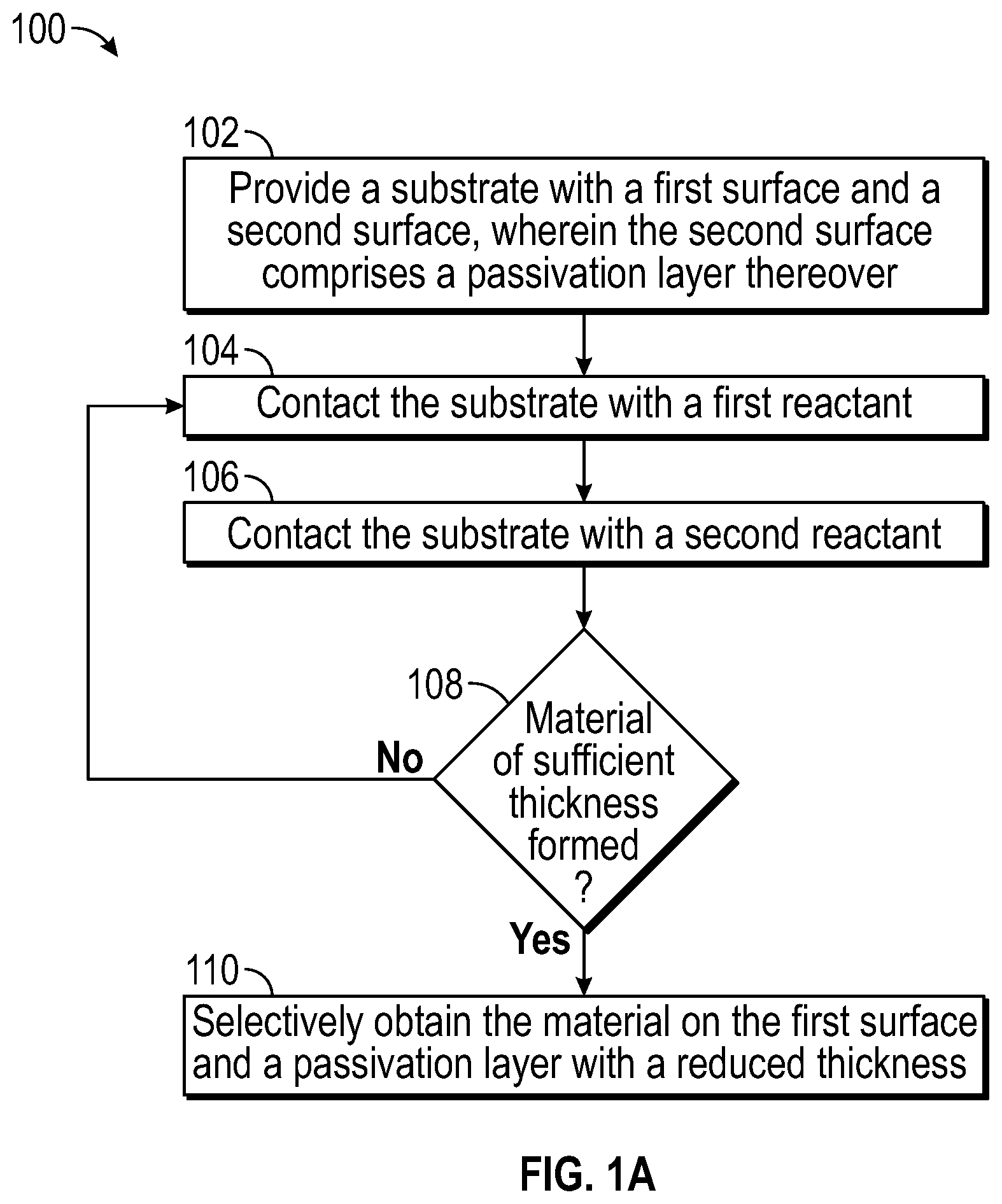
| 9895715 | February 2018 | Haukka et al. |
| 9911595 | March 2018 | Smith et al. |
| 10014212 | July 2018 | Chen et al. |
| 10041166 | August 2018 | Longrie et al. |
| 10049924 | August 2018 | Haukka et al. |
| 10115603 | October 2018 | Niskanen et al. |
| 10157786 | December 2018 | Haukka et al. |
| 10186420 | January 2019 | Fukazawa |
| 10428421 | October 2019 | Haukka et al. |
| 10480064 | November 2019 | Longrie et al. |
| 10546741 | January 2020 | Murakami et al. |
| 2001/0019803 | September 2001 | Mirkanimi |
| 2001/0025205 | September 2001 | Chern et al. |
| 2002/0027261 | March 2002 | Blesser et al. |
| 2002/0047144 | April 2002 | Nguyen et al. |
| 2002/0068458 | June 2002 | Chiang et al. |
| 2002/0090777 | July 2002 | Forbes et al. |
| 2002/0107316 | August 2002 | Bice et al. |
| 2003/0027431 | February 2003 | Sneh et al. |
| 2003/0066487 | April 2003 | Suzuki |
| 2003/0143839 | July 2003 | Raaijmakers et al. |
| 2003/0176559 | September 2003 | Bice et al. |
| 2003/0181035 | September 2003 | Yoon et al. |
| 2003/0185997 | October 2003 | Hsieh |
| 2003/0192090 | October 2003 | Meilland |
| 2003/0193090 | October 2003 | Otani et al. |
| 2004/0092073 | May 2004 | Cabral |
| 2004/0219746 | November 2004 | Vaartstra et al. |
| 2005/0012975 | January 2005 | George et al. |
| 2005/0136604 | June 2005 | Al-Bayati et al. |
| 2005/0160575 | July 2005 | Gambino et al. |
| 2005/0223989 | October 2005 | Lee et al. |
| 2006/0019493 | January 2006 | Li |
| 2006/0047132 | March 2006 | Shenai-Khatkhate et al. |
| 2006/0121271 | June 2006 | Frey et al. |
| 2006/0121733 | June 2006 | Kilpela et al. |
| 2006/0128150 | June 2006 | Gandikota et al. |
| 2006/0141155 | June 2006 | Gordon et al. |
| 2006/0176559 | August 2006 | Minoda et al. |
| 2006/0199399 | September 2006 | Muscat |
| 2006/0226409 | October 2006 | Burr et al. |
| 2006/0292845 | December 2006 | Chiang et al. |
| 2007/0014919 | January 2007 | Hamalainen et al. |
| 2007/0026654 | February 2007 | Huotari et al. |
| 2007/0063317 | March 2007 | Kim et al. |
| 2007/0098894 | May 2007 | Verghese et al. |
| 2007/0099422 | May 2007 | Wijekoon et al. |
| 2007/0232082 | October 2007 | Balseanu et al. |
| 2007/0241390 | October 2007 | Tanaka et al. |
| 2007/0251444 | November 2007 | Gros-Jean et al. |
| 2007/0292604 | December 2007 | Dordi et al. |
| 2008/0066680 | March 2008 | Sherman |
| 2008/0072819 | March 2008 | Rahtu |
| 2008/0124932 | May 2008 | Tateishi et al. |
| 2008/0179741 | July 2008 | Streck et al. |
| 2008/0241575 | October 2008 | Lavoie et al. |
| 2008/0282970 | November 2008 | Heys et al. |
| 2009/0035949 | February 2009 | Niinisto et al. |
| 2009/0071505 | March 2009 | Miya et al. |
| 2009/0081385 | March 2009 | Heys et al. |
| 2009/0203222 | August 2009 | Dussarrat et al. |
| 2009/0269507 | October 2009 | Yu et al. |
| 2009/0274887 | November 2009 | Millward et al. |
| 2009/0311879 | December 2009 | Blasco et al. |
| 2010/0015756 | January 2010 | Weidman et al. |
| 2010/0147396 | June 2010 | Yamagishi et al. |
| 2010/0178468 | July 2010 | Jiang et al. |
| 2010/0248473 | September 2010 | Ishizaka et al. |
| 2010/0270626 | October 2010 | Raisanen |
| 2010/0297474 | November 2010 | Dameron |
| 2010/0314765 | December 2010 | Liang et al. |
| 2011/0053800 | March 2011 | Jung et al. |
| 2011/0120542 | May 2011 | Levy |
| 2011/0124192 | May 2011 | Ganguli et al. |
| 2011/0146568 | June 2011 | Haukka et al. |
| 2011/0146703 | June 2011 | Chen et al. |
| 2011/0221061 | September 2011 | Prakash |
| 2011/0244680 | October 2011 | Tohnoe et al. |
| 2011/0311726 | December 2011 | Liu et al. |
| 2012/0032311 | February 2012 | Gates |
| 2012/0046421 | February 2012 | Darling et al. |
| 2012/0052681 | March 2012 | Marsh |
| 2012/0088369 | April 2012 | Weidman et al. |
| 2012/0189868 | July 2012 | Borovik et al. |
| 2012/0219824 | August 2012 | Prolier et al. |
| 2012/0264291 | October 2012 | Ganguli et al. |
| 2012/0269970 | October 2012 | Ido et al. |
| 2013/0005133 | January 2013 | Lee et al. |
| 2013/0078793 | March 2013 | Sun et al. |
| 2013/0089983 | April 2013 | Sugita et al. |
| 2013/0095664 | April 2013 | Matero et al. |
| 2013/0115763 | May 2013 | Takamure et al. |
| 2013/0115768 | May 2013 | Pore et al. |
| 2013/0126815 | May 2013 | Kim et al. |
| 2013/0143401 | June 2013 | Yu et al. |
| 2013/0146881 | June 2013 | Yamazaki et al. |
| 2013/0189837 | July 2013 | Haukka et al. |
| 2013/0196502 | August 2013 | Haukka et al. |
| 2013/0203267 | August 2013 | Pomarede et al. |
| 2013/0280919 | October 2013 | Yuasa et al. |
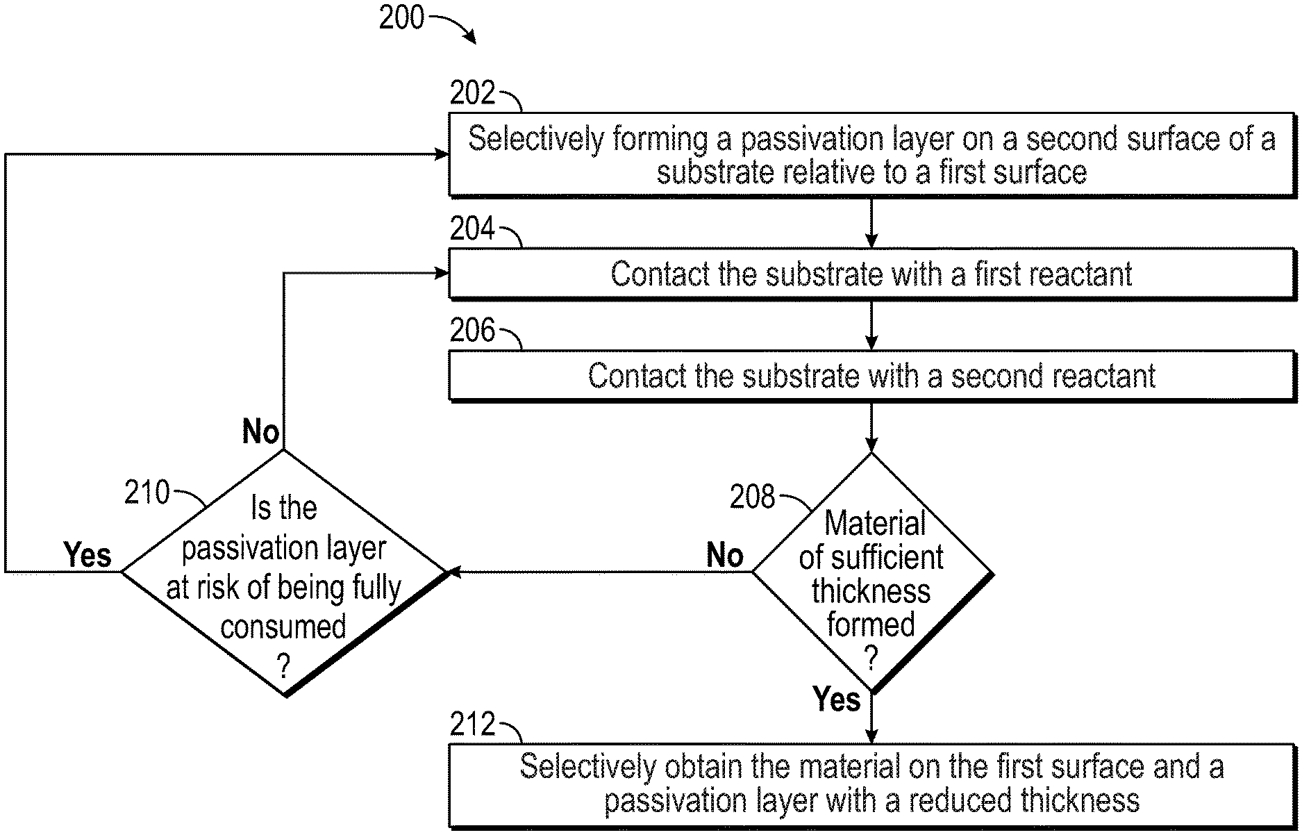
| 2013/0284094 | October 2013 | Pavol et al. |
| 2013/0316080 | November 2013 | Yamaguchi et al. |
| 2013/0323930 | December 2013 | Chattopadhyay et al. |
| 2014/0001572 | January 2014 | Bohr et al. |
| 2014/0024200 | January 2014 | Kato et al. |
| 2014/0091308 | April 2014 | Dasgupta et al. |
| 2014/0120738 | May 2014 | Jung et al. |
| 2014/0152383 | June 2014 | Nikonov et al. |
| 2014/0190409 | July 2014 | Matsumoto et al. |
| 2014/0193598 | July 2014 | Traser et al. |
| 2014/0205766 | July 2014 | Lyon et al. |
| 2014/0209022 | July 2014 | Inoue et al. |
| 2014/0227461 | August 2014 | Darwish et al. |
| 2014/0272194 | September 2014 | Xiao et al. |
| 2014/0273290 | September 2014 | Somervell |
| 2014/0273477 | September 2014 | Niskanen et al. |
| 2014/0273514 | September 2014 | Somervell et al. |
| 2014/0273523 | September 2014 | Rathsack |
| 2014/0273527 | September 2014 | Niskanen et al. |
| 2015/0004806 | January 2015 | Ndiege et al. |
| 2015/0011032 | January 2015 | Kunimatsu et al. |
| 2015/0011093 | January 2015 | Singh et al. |
| 2015/0037972 | February 2015 | Danek et al. |
| 2015/0064931 | March 2015 | Kumagi et al. |
| 2015/0083415 | March 2015 | Monroe et al. |
| 2015/0087158 | March 2015 | Sugita et al. |
| 2015/0093890 | April 2015 | Blackwell et al. |
| 2015/0097292 | April 2015 | He et al. |
| 2015/0118863 | April 2015 | Rathod et al. |
| 2015/0162214 | June 2015 | Thompson et al. |
| 2015/0170961 | June 2015 | Romero et al. |
| 2015/0179798 | June 2015 | Clendenning et al. |
| 2015/0217330 | August 2015 | Haukka |
| 2015/0240121 | August 2015 | Sugita et al. |
| 2015/0275355 | October 2015 | Mallikarjunan et al. |
| 2015/0299848 | October 2015 | Haukka et al. |
| 2015/0371866 | December 2015 | Chen et al. |
| 2015/0376211 | December 2015 | Girard et al. |
| 2016/0075884 | March 2016 | Chen |
| 2016/0079524 | March 2016 | Do et al. |
| 2016/0086850 | March 2016 | Romero et al. |
| 2016/0172189 | June 2016 | Tapily |
| 2016/0186004 | June 2016 | Hustad et al. |
| 2016/0190060 | June 2016 | Bristol et al. |
| 2016/0222504 | August 2016 | Haukka et al. |
| 2016/0247695 | August 2016 | Niskanen et al. |
| 2016/0276208 | September 2016 | Haukka et al. |
| 2016/0284568 | September 2016 | Morris et al. |
| 2016/0293398 | October 2016 | Danek et al. |
| 2016/0346838 | December 2016 | Fujita et al. |
| 2016/0365280 | December 2016 | Brink et al. |
| 2017/0037513 | February 2017 | Haukka et al. |
| 2017/0040164 | February 2017 | Wang et al. |
| 2017/0058401 | March 2017 | Blackwell et al. |
| 2017/0069527 | March 2017 | Haukka et al. |
| 2017/0100742 | April 2017 | Pore et al. |
| 2017/0100743 | April 2017 | Pore et al. |
| 2017/0107413 | April 2017 | Wang et al. |
| 2017/0154806 | June 2017 | Wang et al. |
| 2017/0298503 | October 2017 | Maes et al. |
| 2017/0301542 | October 2017 | Maes et al. |
| 2017/0323776 | November 2017 | Farm et al. |
| 2017/0352533 | December 2017 | Tois et al. |
| 2017/0352550 | December 2017 | Tois et al. |
| 2018/0040708 | February 2018 | Narayanan et al. |
| 2018/0080121 | March 2018 | Longrie et al. |
| 2018/0151345 | May 2018 | Haukka et al. |
| 2018/0151355 | May 2018 | Fukazawa |
| 2018/0182618 | June 2018 | Blanquart et al. |
| 2018/0222933 | August 2018 | Romero |
| 2018/0233350 | August 2018 | Tois et al. |
| 2019/0017170 | January 2019 | Sharma et al. |
| 2019/0057858 | February 2019 | Hausmann et al. |
| 2019/0074441 | March 2019 | Ikuchi et al. |
| 2019/0341245 | November 2019 | Tois et al. |
| 2020/0066512 | February 2020 | Tois et al. |
| 0469456 | Feb 1992 | EP | |||
| 0880168 | Nov 1998 | EP | |||
| 1340269 | Feb 2009 | EP | |||
| 4333900 | Sep 2009 | JP | |||
| 2011-187583 | Sep 2011 | JP | |||
| 2014-93331 | May 2014 | JP | |||
| 102001001072 | Feb 2001 | KR | |||
| 20030027392 | Apr 2003 | KR | |||
| 1020040056026 | Jun 2004 | KR | |||
| 10-0869326 | Nov 2008 | KR | |||
| 10-0920033 | Oct 2009 | KR | |||
| 10-2012-0120902 | Nov 2012 | KR | |||
| 175767 | Aug 2003 | TW | |||
| 2005-39321 | Dec 2005 | TW | |||
| 2010-05827 | Feb 2010 | TW | |||
| 2014-39365 | Oct 2014 | TW | |||
| WO 2002-045167 | Jun 2002 | WO | |||
| WO 2011-156705 | Dec 2011 | WO | |||
| WO 2013-161772 | Oct 2013 | WO | |||
| WO 2014-156782 | Oct 2014 | WO | |||
| WO 2014209390 | Dec 2014 | WO | |||
| WO 2015-047345 | Apr 2015 | WO | |||
| WO 2015094305 | Jun 2015 | WO | |||
| WO 2015147843 | Oct 2015 | WO | |||
| WO 2015147858 | Oct 2015 | WO | |||
| WO 2017-184357 | Oct 2017 | WO | |||
| WO 2017-184358 | Oct 2017 | WO | |||
| WO 2018-204709 | Nov 2018 | WO | |||
| WO 2018-213018 | Nov 2018 | WO | |||
Other References
|
Aaltonen et al., "Atomic Layer Deposition of Iridium Thin Films", Journal of the Electrochemical Society, 151 (8) G489-G492 (2004). cited by applicant . Au et al., "Selective Chemical Vapor Deposition of Manganese Self-Aligned Capping Layer for Cu Interconnections in Microelectronics", Journal of the Electrochemical Society, vol. 157, No. 6, 2010, pp. D341-D345. cited by applicant . Benzotriazole, Wikipedia via https:--en.wikipedia.org-wiki-Benzotriazole; pp. 1-5, no date available. cited by applicant . Bernal-Ramos, et al., "Atomic Layer Deposition of Cobalt Silicide Thin Films Studied by in Situ Infrared Spectroscopy", Chem. Mater. 2015, 27, pp. 4943-4949. cited by applicant . Bouteville et al., "Selective R.T.L.P.C.V.D. of Tungsten by Silane Reduction on Patterned PPQ-Si Wafers" Journal De Physique IV, Colloque C2, suppl. au Journal de Physique II, vol. 1, Sep. 1991, pp. C2-857-C2-864. cited by applicant . Burton, B.B. et al., "Atomic Layer Deposition of MgO Using Bis(ethylcyclopentadienyl)magnesium and H20". J. Phys. Chem. C, 2009, 113, 1939-1946. cited by applicant . Burton, B.B., et al., "Si02 Atomic Layer Deposition Using Tris(dimethylamino)silane and Hydrogen Peroxide Studied by in Situ Transmission FTIR Spectroscopy". J. Phys. Chem. C, 2009, 113, 8249-8257. cited by applicant . Carlsson, J., "Precursor Design for Chemical Vapour Deposition", Acta Chemica Scandinavica, vol. 45, 1991, pp. 864-869. cited by applicant . Chang et al, "Influences of damage and contamination from reactive ion etching on selective tungsten deposition in a low-pressure chemical-vapor-deposition reactor", J. Appl. Phys., vol. 80, No. 5, Sep. 1, 1996, pp. 3056-3061. cited by applicant . Chen et al., Highly Stable Monolayer Resists for Atomic Layer Deposition on Germanium and Silicon, Chem. Matter, vol. 18, No. 16, pp. 3733-3741, 2006. cited by applicant . Cho et al., "Atomic layer deposition of Al.sub.2O.sub.3 thin films using dimethylaluminum isopropoxide and water", Journal of Vacuum Science & Technology A 21, (2003), doi: 10.1116-1.1562184, pp. 1366-1370. cited by applicant . Coclite, et al.; 25th Anniversary Article: CVD Polymers: A New Paradigm for Surface Modification and Device Fabrication; Advanced Materials; Oct. 2013; 25; pp. 5392-5423. cited by applicant . Elam et al., "Kinetics of the WF6 and Si2H6 surface reactions during tungsten atomic layer deposition", Surface Science, vol. 479, 2001, pp. 121-135. cited by applicant . Elam et al., "Nucleation and growth during tungsten atomic layer deposition on SiO2 surfaces", Thin Solid Films, vol. 386, 2001 pp. 41-52. cited by applicant . Ellinger et al., "Selective Area Spatial Atomic Layer Deposition of ZnO, Al2O3, and Aluminum-Doped ZnO Using Poly(vinyl pyrrolidone)", Chem. Mater. 2014, 26, pp. 1514-1522. cited by applicant . Fabreguette et al., Quartz crystal microbalance study of tungsten atomic layer deposition using WF6 and Si2H6, Thin Solid Films, vol. 488, 2005, pp. 103-110. cited by applicant . Farm et al. Selective-Area Atomic Layer Deposition Using Poly( methyl methacrylate) Films as Mask Layers, J. Phys. Chem. C, 2008, 112, pp. 15791-15795. (Year: 2008). cited by applicant . Farm et al., "Self-Assembled Octadecyltrimethoxysilane Monolayers Enabling Selective-Area Atomic Layer Deposition of Iridium", Chem. Vap. Deposition, 2006, 12, pp. 415-417. cited by applicant . Farr, Isaac Vincent; Synthesis and Characterization of Novel Polyimide Gas Separation Membrane Material Systems, Chapter 2; Virginia Tech Chemistry PhD Dissertation; URN# etd-080999-123034; Jul. 26, 1999. cited by applicant . Formic Acid, Wikipedia via https:--en.wikipedia.org-wiki-Formic_acid; pp. 1-5, no date available. cited by applicant . George, Steven M., "Atomic Layer Deposition: An Overview", Chem. Rev. 2010, 110, pp. 111-113. cited by applicant . Ghosal et al., Controlling Atomic Layer Deposition of Ti02 in Aerogels through Surface Functionalization, Chem. Matter, vol. 21, pp. 1989-1992, 2009. cited by applicant . Grubbs et al., "Nucleation and growth during the atomic layer deposition of W on Al2O3 and Al2O3 on W", Thin Solid Films, vol. 467, 2004, pp. 16-27. cited by applicant . Hashemi et al., "A New Resist for Area Selective Atomic and Molecular Layer Deposition on Metal-Dielectric Patterns", J. Phys. Chem. C 2014, 118, pp. 10957-10962. cited by applicant . Hashemi et al., "Selective Deposition of Dieletrics: Limits and Advantages of Alkanethiol Blocking Agents on Metal-Dielectric Patterns", ACS Appl. Mater. Interfaces 2016, 8, pp. 33264-33272. cited by applicant . Hymes et al., "Surface cleaning of copper by thermal and plasma treatment in reducing and inert ambients", J. Vac. Sci. Technol. B, vol. 16, No. 3, May-Jun. 1998, pp. 1107-1109. cited by applicant . International Search Report and Written Opinion dated Feb. 17, 2012 in Application No. PCT-US2011-039970, filed Jun. 10, 2011. cited by applicant . International Search Report and Written Opinion dated Aug. 8, 2018 in Application No. PCT-US2018-030974, filed May 3, 2018. cited by applicant . International Search Report and Written Opinion dated Jul. 24, 2018 in Application No. PCT-US2018-030979, filed May 3, 2018. cited by applicant . Klaus et al., "Atomic layer deposition of tungsten using sequential surface chemistry with a sacrificial stripping reaction", Thin Solid Films, vol. 360, 2000, pp. 145-153. cited by applicant . Klaus et al., "Atomically controlled growth of tungsten and tungsten nitride using sequential surface reactions", Applied Surface Science 162-163, 2000, pp. 479-491. cited by applicant . King, "Dielectric Barrier, Etch Stop, and Metal Capping Materials for State of the Art and beyond Metal Interconnects", ECS Journal of Solid State Science and Technology, vol. 4, Issue 1, pp. N3029-N3047, 2015. cited by applicant . Kukli et al., "Properties of hafnium oxide films grown by atomic layer deposition from hafnium tetraiodide and oxygen", J. Appl. Phys., vol. 92, No. 10, 15 Nov. 2002, pp. 5698-5703. cited by applicant . Lecordier et al., "Vapor-deposited octadecanethlol masking layer on copper to enable area selective Hf3N4 atomic layer deposition on dielectrics studied by in situ spectroscopic ellipsometry", J. Vac. Sci. Technol. A36(3), May-Jun. 2018, pp. 031605-1-031605-8. cited by applicant . Lee et al., Area-Selective Atomic Layor Deposition Using Self-Assembled Monolayer and Scanning Probe Lithography, Journal of the Electrochemical Society, vol. 156, Issue 9, pp. G125-G128, 2009. cited by applicant . Lei et al., "Real-time observation and opitimization of tungsten atomic layer deposition process cycle", J. Vac. Sci. Technol. B, vol. 24, No. 2, Mar.-Apr. 2006, pp. 780-789. cited by applicant . Lemonds, Andrew Michael, "Atomic Layer Deposition and Properties of Refractory Transition Metal-Based Copper-Diffusion Barriers for ULSI Interconnect", The University of Texas at Austin, 2003, pp. 1-197. cited by applicant . Lemonds, A.M., "Atomic layer deposition of TaSix thin films on SiO2 using TaF5 and Si2H6", Thin Solid Films 488, 2005 pp. 9-14. cited by applicant . Leusink et al., "Growth kinetics and inhibition of growth of chemical vapor deposited thin tungsten films on silicon from tungsten hexafluoride", J. Appl. Phys., vol. 72, No. 2, Jul. 15, 1992, pp. 490-498. cited by applicant . Liang, Xuehai, et al., "Growth of Ge Nanofilms Using Electrochemical Atomic Layer Deposition, with a "Bait and Switch" Surface-Limited Reaction". Journal of the American Chemical Society, 2011, 133, 8199-8024. cited by applicant . Lohokare et al., "Reactions of Disilane on Cu(111): Direct Observation of Competitive Dissociation, Disproportionation, and Thin Film Growth Processes", Langmuir 1995, vol. 11, pp. 3902-3912. cited by applicant . Low et al., Selective deposition of CVD iron on silicon dioxide and tungsten, Microelectronic Engineering 83, pp. 2229-2233, 2006. cited by applicant . Mackus et al., Influence of Oxygen Exposure on the Nucleation of Platinum Atomic Layer Deposition: Consequences for Film Growth, Nanopatterning, and Nanoparticle Synthesis, Chem. Matter, vol. 25, pp. 1905-1911, 2013. cited by applicant . Mackus et al., Local deposition of high-purity Pt nanostructures by combining electron beam induced deposition and atomic layer deposition, Journal of Applied Physics, vol. 107, pp. 116102-1-116102-3, 2010. cited by applicant . Mackus et al., "The use of atomic layer deposition in advanced nanopatterning", Nanoscale, 2014, 6, pp. 10941-10960. cited by applicant . Maluf et al., "Selective tungsten filling of sub-0.25 .mu.m trenches for the fabrication of scaled contacts and x-ray masks", J. Vac. Sci. Technol. B, vol. 8, No. 3, May-Jun. 1990, pp. 568-569. cited by applicant . Norrman, et al.; 6 Studies of Spin-Coated Polymer Films; Annu. Rep. Prag. Chem.; Sect. C; 2005; 101; pp. 174-201. cited by applicant . Office Action dated Jun. 8, 2017 in Korean Application No. 2013-7000596. cited by applicant . Overhage et al., Selective Atomic Layer Deposition (SALD) of Titanium Dioxide on Silicon and Copper Patterned Substrates, Journal of Undergraduate Research 4, 29, Mar. 2011 in 4 pages. cited by applicant . Parulekar et al., Atomic Layer Deposition of Zirconium Oxide on Copper Patterned Silicon Substrate, Journal of Undergraduate Research, vol. 7, pp. 15-17, 2014. cited by applicant . Parulekar et al., Selective atomic layer deposition of zirconium oxide on copper patterned silicon substrate, pp. 1-6, 2013. cited by applicant . Prasittichai et al., "Area Selective Molecular Layer Deposition of Polyurea Film", Applied Materials & Interfaces, 2013, vol. 5, pp. 13391-13396. cited by applicant . Proslier et al., "Atomic Layer Deposition and Superconducting Properties of NbSi Films", The Journal of Physical Chemistry C, 2011, vol. 115, No. 50, pp. 1-26. cited by applicant . Putkonen, et al.; Atomic Layer Deposition of Polyimide Thin Films; Journal of Materials Chemistry; 2007, 17, pp. 664-669. cited by applicant . Ratta, Varun; Crystallization, Morphology, Thermal Stability and Adhesive Properties of Novel High Performance Semicrystalline Polyimides, Chapter 1; Virginia Tech Chemistry PhD Dissertation; URN # etd-051799-162256; Apr. 26, 1999. cited by applicant . Roberts et al., "Selective Mn deposition on Cu lines", poster presentation, 12th International Conference on Atomic Layer Deposition, Jun. 19, 2012, Dresden, Germany. cited by applicant . Sapp, et al.; Thermo-Mechanical and Electrical Characterization of Through-Silicon Vias with a Vapor Deposited Polyimide Dielectric Liner; IEEE; 2012. cited by applicant . Schmei er, Decomposition of formic acid, Chemnitz University of Technology, pp. 1-13, Aug. 31, 2011. cited by applicant . Schmei er, Reduction of Copper Oxide by Formic Acid an ab-initio study, Chemnitz University of Technology, pp. 1-42, Sep. 2011. cited by applicant . Schuisky et al., "Atomic layer deposition of thin films using O2 as oxygen source," Langmuir, 2001, vol. 17, pp. 5508-5512. cited by applicant . Selvaraj et al., Selective atomic layer deposition of zirconia on copper patterned silicon substrates using ethanol as oxygen source as well as copper reductant, Journal of Vacuum Science & Technology A, vol. 32, No. 1, pp. 010601-1-010601-4, Jan. 2014. cited by applicant . Senesky et al., "Aluminum nitride as a masking material for the plasma etching of silicon carbide structures," 2010, IEEE, pp. 352-355. cited by applicant . Sundberg, et al.; Organic and Inorganic-Organic Thin Film Structures by Molecular Layer Deposition: A Review; Beilstein J. Nanotechnol; 2014, 5, pp. 1104-1136. cited by applicant . Suntola, Tuomo, "Thin Films and Epitaxy Part B: Grown mechanism and Dynamics", Handbook of Crystal Growth vol. 3, Elsevier, 1994, 33 pages. cited by applicant . Ting, et al., "Selective Electroless Metal Deposition for Integrated Circuit Fabrication", J. Electrochem. Soc., vol. 136, No. 2, Feb. 1989, pp. 456-462. cited by applicant . Toirov, et al.; Thermal Cyclodehydration of Polyamic Acid Initiated by UV-Irradiation; Iranian Polymer Journal; vol. 5, No. 1; pp. 1A323:C3286-22; 1996; Iran. cited by applicant . "Tungsten and Tungsten Silicide Chemical Vapor Deposition", TimeDomain CVD, Inc., retrieved from link: http:--www.timedomaincvd.com-CVD_Fundamentals-films-W_WSi.html, Last modified Jul. 11, 2008. cited by applicant . Yu et al., "Gas-surface reactions in the chemical vapor deposition of tungsten using WF6--SiH4 mixtures", J. Vac. Sci. Technol. A, vol. 7, No. 3, May-Jun. 1989, pp. 625-629. cited by applicant . Vallat et al., Selective deposition of Ta205 by adding plasma etching super-cycles in plasma enhanced atomic layer deposition steps, Journal of Vacuum Science & Technology A, vol. 35, No. 1, pp. 01B104-1-01B104-7, Jan. 2017. cited by applicant . Vervuurt et al., "Area-selective atomic layer deposition of platinum using photosensitive polyimide", Nanotechnology 27, 2016, in 6 pages. cited by applicant . Zhou, et al.; Fabrication of Organic Interfacial Layers by Molecular Layer Deposition: Present Status and Future Opportunities; Journal of Vacuum Science & Technology; A 31 (4), 040801-1 to 040801-18; 2013. cited by applicant. |
Primary Examiner: Mehta; Ratisha
Attorney, Agent or Firm: Knobbe, Martens, Olson & Bear, LLP
Parent Case Text
CROSS-REFERENCE TO RELATED APPLICATIONS
The present application claims priority to U.S. provisional application No. 62/666,039, filed May 2, 2018, the disclosure of which is incorporated herein by reference in its entirety for all purposes.
Claims
What is claimed is:
1. An atomic layer deposition (ALD) process for selectively forming a dielectric material on a first surface of a patterned substrate, comprising: providing a substrate comprising a first surface and a second surface, wherein the second surface comprises a passivation layer thereover; conducting at least one deposition cycle comprising alternately and sequentially contacting the substrate with a first precursor and a second reactant comprising oxygen; wherein the second reactant reacts with the first precursor to form a dielectric material on the first surface; and wherein the passivation layer is ashed by the second reactant during each deposition cycle.
2. The method of claim 1, wherein the first surface is a dielectric surface.
3. The method of claim 1, wherein the first surface comprises a low-k material.
4. The method of claim 1, wherein the second surface is a metal surface.
5. The method of claim 1, wherein the dielectric material comprises silicon oxide.
6. The method of claim 1, wherein the dielectric material comprises a metal oxide.
7. The method of claim 1, wherein the first precursor is an alkylaminosilane.
8. The method of claim 1, wherein the passivation layer comprises an organic material.
9. The method of claim 1, wherein the passivation layer is selectively deposited on the second surface relative to the first surface prior to beginning the first deposition cycle.
10. The method of claim 1, wherein the deposition cycle is repeated a plurality of times to form an oxide film of a desired thickness on the dielectric surface.
11. The method of claim 10, further comprising the selective deposition of additional passivation layer to the passivation layer between the beginning and end of each deposition cycle.
12. The method of claim 1, wherein the at least one deposition cycle begins with contacting the substrate with the second reactant before contact with the first precursor.
13. The method of claim 1, wherein contacting the substrate with the second reactant further comprises activating the second reactant with plasma.
14. The method of claim 1, wherein the dielectric material is selectively formed on the first surface relative to the passivation layer.
15. The method of claim 1, wherein the dielectric material is formed on the passivation layer and wherein the dielectric material is removed from the passivation layer with the ashing of the passivation layer, thereby selectively forming the dielectric material on the first surface.
16. A cyclical deposition process for selectively a forming a material on a surface of a patterned substrate, comprising: providing a substrate comprising a first surface and a second surface, wherein the second surface comprises a passivation layer thereover; conducting at least one deposition cycle comprising alternately and sequentially contacting the substrate with a first precursor and a second reactant; wherein the second reactant reacts with the first precursor to form the material on the first surface; and wherein the passivation layer is etched by the second reactant during each deposition cycle.
17. The cyclical deposition process of claim 16, wherein the second reactant comprises plasma-activated species.
18. The cyclical deposition process of claim 17, wherein the second reactant comprises oxygen, the passivation layer comprises an organic layer, and etching comprises ashing.
19. The cyclical deposition process of claim 16, wherein deposition is halted before the etching of the passivation layer exposes the second surface.
20. The cyclical deposition process of claim 19, further comprising further depositing additional passivation layer over the second surface after halting the deposition and prior to continuing the deposition.
21. A plasma enhanced atomic layer deposition (PEALD) process for selectively forming an oxide material on a first dielectric surface of a patterned substrate, comprising: providing a substrate comprising a first dielectric surface and a second metallic surface, wherein the second metallic surface comprises an organic passivation layer thereover; conducting at least one deposition cycle comprising alternately and sequentially contacting the substrate with a first precursor and a second reactant comprising oxygen and plasma; wherein the second reactant reacts with the first precursor to form an oxide material on the first dielectric surface; and wherein the organic passivation layer is ashed by the second reactant during each deposition cycle.
Description
BACKGROUND
Field
The present disclosure relates generally to the field of semiconductor device manufacturing and, more particularly, to selective formation of layers employing deposition and removal of films.
Description of the Related Art
In the semiconductor industry, there is an increasing need for selective processes. For example, film growth may be desired on one surface but not on a second, different surface. These two different surfaces can comprise different materials, for example a metal and a dielectric. Good selective processes could reduce the number process steps by avoiding more complicated processes for separate patterning of the deposited material, such as photolithographic masking and patterning, thus saving time and money.
SUMMARY
In one aspect a method is provided for an atomic layer deposition (ALD) process for selectively forming a dielectric material on a first surface of a patterned substrate. The method includes providing a substrate comprising a first surface and a second surface, wherein the second surface comprises a passivation layer thereover. The method further includes conducting at least one deposition cycle comprising alternately and sequentially contacting the substrate with a first precursor and a second reactant comprising oxygen. The method further includes wherein the second reactant reacts with the first precursor to form a dielectric material on the first surface, and wherein the passivation layer is ashed by the second reactant during each deposition cycle.
In some embodiments, the method for an ALD process further includes wherein the first surface is a dielectric surface. In some embodiments, the dielectric surface comprises silicon oxide. In some embodiments, the first surface comprises a low-k material. In some embodiments, the second surface is a metal surface. In some embodiments, the metal surface comprises at least one of Co, Cu or W. In some embodiments, the dielectric material is an oxide. In some embodiments, the oxide is silicon oxide. In some embodiments, the oxide is a metal oxide.
In some embodiments, the first precursor comprises a metal precursor, a silicon precursor, or mixtures thereof. In some embodiments, the first precursor is an alkylaminosilane.
In some embodiments, the passivation layer comprises an organic material. In some embodiments, the passivation layer is selectively deposited on the second surface relative to the first surface prior to beginning the first deposition cycle. In some embodiments, the deposition cycle is repeated a plurality of times to form an oxide film of a desired thickness on the dielectric surface. In some embodiments, additional passivation layer is selectively deposited on the passivation layer between the beginning and end of each deposition cycle.
In some embodiments, the ALD process is a plasma enhanced atomic layer deposition (PEALD) process. In some embodiments, the at least one deposition cycle begins with contacting the substrate with the second reactant before contact with the first precursor. In some embodiments, the at least one deposition cycle further comprises contacting the substrate with at least one additional reactant in each cycle. In some embodiments, the second reactant further comprises plasma. In some embodiments, contacting the substrate with the second reactant further comprises activating the second reactant with plasma.
In some embodiments, the dielectric material is selectively formed on the first surface relative to the passivation layer. In some embodiments, the dielectric material is formed on the passivation layer and the dielectric material is removed from the passivation layer with the ashing of the passivation layer, thereby selectively forming the dielectric material on the first surface.
In another aspect a cyclical deposition process is provided for selectively a forming a material on a surface of a patterned substrate. The method includes providing a substrate comprising a first surface and a second surface, wherein the second surface comprises a passivation layer thereover. The method further includes conducting at least one deposition cycle comprising alternately and sequentially contacting the substrate with a first precursor and a second reactant. The second reactant reacts with the first precursor to form the material on the first surface, and the passivation layer is etched by the second reactant during each deposition cycle.
In some embodiments, the process comprises atomic layer deposition (ALD). In some embodiments, the process comprises plasma enhanced ALD (PEALD). In some embodiments, the second reactant comprises plasma-activated species. In some embodiments, the second reactant comprises oxygen, the passivation layer comprises an organic layer, and etching comprises ashing. In some embodiments, the passivation layer comprises a polymer.
In some embodiments, deposition is halted before the etching of the passivation layer exposes the second surface. In some embodiments, the method includes further depositing additional passivation layer over the second surface after halting the deposition and prior to continuing the deposition.
In another aspect a plasma enhanced atomic layer deposition (PEALD) process is provided for selectively forming an oxide material on a first dielectric surface of a patterned substrate. The method includes providing a substrate comprising a first dielectric surface and a second metallic surface, wherein the second metallic surface comprises an organic passivation layer thereover. The method further includes conducting at least one deposition cycle comprising alternately and sequentially contacting the substrate with a first precursor and a second reactant comprising oxygen and plasma. The second reactant reacts with the first precursor to form an oxide material on the first dielectric surface, and the organic passivation layer is ashed by the second reactant during each deposition cycle.
BRIEF DESCRIPTION OF THE DRAWINGS
FIG. 1A is a flow diagram illustrating a selective deposition process for depositing a material on a first surface while reducing the thickness of a passivation layer over a second surface.
FIG. 1B is a flow diagram illustrating a selective deposition process for depositing a material on a first surface while reducing the thickness of a passivation layer selectively deposited over a second surface.
FIG. 2 is a graph of some embodiments showing the thickness of a polyimide layer versus the number of cycles of oxidation performed, wherein a passivation ash rate is calculated.
FIG. 3 illustrates the selective deposition of a material on a first surface of a substrate by a cyclical deposition process, while the cyclical deposition process removes a passivation layer over a second surface.
DETAILED DESCRIPTION
Dielectric films, such as metal oxide or silicon oxide (e.g., SiO) films, have a wide variety of applications, as will be apparent to the skilled artisan, for example in integrated circuit fabrication. According to some embodiments of the present disclosure, various dielectric films, particularly oxide films, precursors, and methods for depositing such films are provided.
In some embodiments, a material is formed on a first surface of a substrate relative to a second surface by a selective deposition process. In some embodiments, the material is an oxide material. In some embodiments, a dielectric film is formed selectively using a cyclical deposition process on a dielectric surface of a substrate relative to a passivation layer on a metal surface.
For example, FIG. 1A is a flow diagram 100 illustrating a selective deposition process of depositing a material on a first surface while reducing the thickness of a passivation layer over a second surface. In the first illustrated block 102 a substrate with a first surface and a second surface is provided, wherein the second surface comprises a passivation layer thereover. In block 104 the substrate is contacted with a first reactant, and in block 106 the substrate is contacted with a second reactant. In some embodiments, blocks 104 and 106 are performed alternately and sequentially. In illustrated decision block 108, the substrate may be repeatedly exposed to the first and second reactants in blocks 104 and 106 until a material of sufficient thickness is formed. In some embodiments, a sufficiently thick material is formed and therefore blocks 104 and 106 are not repeated. In some embodiments, a sufficiently thick material is not formed and therefore blocks 104 and 106 are repeated, and the repetition of blocks 104 and 106 is referred to as a cyclical deposition process. Blocks 104 and 106 need not be in the same sequence nor identically performed in each repetition. In some embodiments, blocks 104 and 106 are performed consecutively. In some embodiments, blocks 104 and 106 are separated by one or more intermittent processes. In some embodiments, the repetition of blocks 104 and 106 are performed consecutively. In some embodiments, the repetition of blocks 104 and 106 is separated by one or more intermittent processes. In some embodiments, intermittent processes may be selected from at least one of excess reactant and byproduct removal (e.g., vacuum and/or inert gas purge), selective deposition of an additional passivation layer, additional clean up etch, repeated exposure of the same reactant prior to exposure of another reactant, and/or exposure to an additional reactant in some or all cycles. Intervening removal of excess reactant and byproduct aids in separating the supply of different reactants to minimize risk of gas phase interaction and limit the deposition reactions to surface reactions. Skilled artisans will appreciate that some interactions with residual gases may be tolerated in order to minimize duration of the intervening removal (e.g., purge) steps. Avoiding overlap in the supply of reactants to the reaction space typically reduces gas phase reactions sufficiently, and optimization of flow paths together with intervening purging can further minimize residual gas interactions. Once a desired material is thickness is formed, the selective deposition process is completed in block 110, where the material is selectively obtained on a first surface and a passivation layer with a reduced thickness is obtained on the second surface. Reactants can be precursors that leave one or more elements in the deposited film. In some embodiments, one or more reactants can serve to chemically reduce, oxidize or getter products of the deposited material.
Similar to FIG. 1A, FIG. 1B is an example flow diagram 200 illustrating the selective deposition of a material on a first surface while reducing the thickness of a passivation layer, however FIG. 1B includes selectively forming a passivation layer on a second surface. It is to be understood that any of the same or similar features or functions discussed with regard to FIG. 1A may also be applied to the same or similar features or functions of FIG. 1B. In the first illustrated block 202 a passivation layer is selectively formed on a second surface of a substrate relative to a first surface. In block 204 the substrate is contacted with a first reactant, and in block 206 the substrate is contacted with a second reactant. In illustrated decision block 208, a sufficiently thick material may be formed and therefore the material is selectively obtained on the first surface with a passivation layer of a reduced thickness as shown in block 212. If a sufficiently thick material is not yet formed and if the passivation layer is not at risk of being fully consumed by exposure to the reactants, decision block 210 illustrates that the substrate may be repeatedly and alternately exposed to the first and second reactants in blocks 204 and 206. Alternatively, if the passivation layer is at risk of being fully consumed by exposure to the reactants, decision block 210 illustrates that first illustrated block 202 may be repeated where a passivation layer is selectively formed on a second surface of a substrate relative to a first surface before the substrate is exposed to the first and second reactants in blocks 204 and 206.
In some embodiments, the cyclical deposition process is atomic layer deposition (ALD). In some embodiments, the cyclical deposition process is cyclical chemical vapor deposition (CVD). In some embodiments, the passivation layer was previously deposited on the second surface (for example, the metal surface). In some embodiments, the passivation layer is partially removed during the cyclical deposition process. During an ALD process, for example, the passivation layer may be slowly removed, such as by etching, during ALD phases. For example, for an organic (e.g., polymer) passivation layer, etching (e.g., ashing) may be accomplished during deposition phases in which oxidants are supplied, while simultaneously a dielectric film is deposited on the dielectric surface. In another example, a passivation layer is simultaneously removed while an oxide material is deposited on the dielectric surface during exposure of the substrate to a second reactant in the ALD process. The slow etching of the passivation layer may prevent deposition of the dielectric on the passivation layer and on the metal.
In some embodiments, the ALD process may be a plasma enhanced atomic layer deposition process (PEALD). In some embodiments, plasma power is provided to generate more reactive species from reactants containing oxygen. In some embodiments, reactant containing oxygen comprises O.sub.2 gas, which is subjected to plasma generating power. In some embodiments, the plasma may be generated remotely from the deposition chamber and plasma products supplied to the deposition chamber. In some remote plasma embodiments, the delivery path optimizes delivery of neutral O species while minimizing ion delivery to the substrate. In some embodiments, the plasma may be generated in situ within the deposition chamber.
In some embodiments, the first surface of the substrate comprises a dielectric surface. In some embodiments, the dielectric surface of the substrate comprises a silicon oxide (e.g., SiO.sub.2). In some embodiments, the dielectric surface of the substrate comprises a low-k material.
In some embodiments, the second surface comprises a metal surface. Unless otherwise indicated, if a surface is referred to as a metal surface herein, it may be a metal surface or a metallic surface. In some embodiments the metal or metallic surface may comprise metal, metal oxides, and/or mixtures thereof. In some embodiments the metal or metallic surface may comprise surface oxidation. In some embodiments the metal or metallic material of the metal or metallic surface is electrically conductive with or without surface oxidation. In some embodiments metal or a metallic surface comprises one or more transition metals. In some embodiments the metal or metallic surface comprises one or more of Al, Cu, Co, Ni, W, Nb, Fe. In some embodiments the metal or metallic surface comprises at least one of Co, Cu or W. In some embodiments the metal or metallic surface comprises one or more noble metals, such as Ru. In some embodiments the metal or metallic surface comprises a conductive metal oxide, nitride, carbide, boride, or combination thereof. For example, the metal or metallic surface may comprise one or more of RuO.sub.x, NbC.sub.x, NbB.sub.x, NiO.sub.x, CoO.sub.x, NbO.sub.x and WNC.sub.x. In some embodiments the substrate may comprise a metal nitride, including, but not limited to TiN and/or TaN. In some embodiments the metal surface may comprise a metal carbide, including, but not limited to TiC and/or TaC. In some embodiments the metal surface may comprise a metal chalcogenide, including, but not limited to MoS.sub.2, Sb.sub.2Te.sub.3, and/or GeTe. In some embodiments the metal surface is a TiN surface. In some embodiments the metal surface is a W surface.
Selectivity
Selectivity can be given as a percentage calculated by [(deposition on first surface)-(deposition on second surface)]/(deposition on the first surface). Deposition can be measured in any of a variety of ways. In some embodiments deposition may be given as the measured thickness of the deposited material. In some embodiments deposition may be given as the measured amount of material deposited.
In some embodiments selectivity is greater than about 10%, greater than about 50%, greater than about 75%, greater than about 85%, greater than about 90%, greater than about 93%, greater than about 95%, greater than about 98%, greater than about 99% or even greater than about 99.5%. In embodiments described herein, the selectivity can change over the duration or thickness of a deposition.
In some embodiments deposition of the dielectric, such as an oxide, only occurs on the first dielectric surface and does not occur on the passivation layer over the second metal surface. In some embodiments deposition on the first surface of the substrate relative to the passivation layer is at least about 80% selective, which may be selective enough for some particular applications. In some embodiments the deposition on the first surface of the substrate relative to the passivation layer is at least about 50% selective, which may be selective enough for some particular applications. In some embodiments the deposition on the first surface of the substrate relative to the passivation layer is at least about 10% selective, which may be selective enough for some particular applications.
In some embodiments the passivation layer may be selectively formed on the metal surface prior to selective deposition of the dielectric material on the dielectric surface. For example, in some embodiments, a passivation layer may be blanket deposited on a patterned substrate, and patterned and etched by traditional processes to leave the passivation layer selectively where the subsequent deposition is to be avoided, such as over a metal surface. In other embodiments, a passivation layer may be selectively deposited on a metal layer. Selective deposition of a passivation layer may be carried out, for example, as described below, and as described in US Patent Publication No. 2017-0352533 A1 (application Ser. No. 15/170,769) or US Patent Publication No. 2017-0352550 A1 (application Ser. No. 15/486,124), the entire disclosure of each of which is incorporated by reference herein in its entirety.
As noted above, the selective formation of the passivation layer over metal surfaces need not be 100% selective in order to achieve 100% selectivity. For example, the passivation layer deposition may be partially selective such that it is formed to be thicker over the metal surface than over the dielectric surface. A subsequent short, timed etch of the passivation material may be conducted for a duration to expose the dielectric surface while leaving some passivation layer covering the metal surface.
ALD Process
According to some embodiments, a dielectric film is deposited on a first surface of a substrate with an oxygen based ALD process. In some embodiments, the deposited dielectric film may be, for example, silicon oxide (e.g., SiO.sub.2) or other metal oxide that can be grown with a PEALD process. In some embodiments, the deposited dielectric film can comprise SiO.sub.2, TiO.sub.2, ZrO.sub.2, HfO.sub.2, Nb.sub.2O.sub.5, Ta.sub.2O.sub.5, WO.sub.3, NiO and combinations thereof. The second surface of the substrate may be covered by a passivation layer. In some embodiments, the passivation layer is an organic layer. The organic passivation layer may be a polymer, such as polyimide or polyamide.
In some embodiments, an oxide material film is deposited on a first surface of a substrate with an oxygen based ALD process. In some embodiments, the deposited oxide material film may be a conductive oxide film. For example, in some embodiments the conductive oxide film is an indium tin oxide (ITO) film. In some embodiments, the deposited oxide material film may be a dielectric film, as described herein.
In some embodiments, the passivation layer inhibits oxide material film and/or dielectric film deposition there. However, in some embodiments, the passivation layer does not inhibit deposition of the oxide material film or dielectric film, that is, the oxide material film or dielectric film chemistry may not be selective as between the underlying dielectric substrate surface and the passivation layer. This is due to the fact that conditions are selected to ensure some removal of the passivation layer during the ALD process, thus undercutting and removing any deposition of the oxide material film or dielectric film over the passivation layer. As the passivation layer is sacrificial, the passivation layer is slowly removed (e.g., etched) during one of the cyclical deposition phases. For example, in an ALD sequence, an organic (e.g., polymer) passivation layer may be slowly ashed by an oxidant phase of the ALD sequence, which prevents oxide material film or dielectric film growth on the passivation layer. In another example, in an ALD sequence, a passivation layer is removed during exposure of the substrate to a second reactant in the ALD process, which prevents oxide material film or dielectric film growth on the passivation layer. Relative to the growth over the passivation layer, the oxide material film or dielectric film is deposited normally (non-selectively, or with low selectivity) on the dielectric surface. Regardless of whether the oxide material film or dielectric material is deposited normally or selectively on the dielectric surface, slowly etching (e.g., ashing) the sacrificial passivation layer by an oxidant phase of the ALD sequence has the end effect of selectively forming the oxide material film or dielectric material on the dielectric substrate relative to the passivation layer. Thus, using the process of FIG. 1A or 1B can effectively increase selectivity of the formation of the oxide material film or dielectric film.
In some embodiments, before deposition of the oxide material film or dielectric film is performed but after the passivation layer is formed, any passivation layer remaining on the dielectric surface can be removed with a plasma pretreatment with suitable parameters. In some embodiments, rather than a separate process to remove any passivation material from over the dielectric surface, any passivation layer remaining on the dielectric surface is removed by initial phases of the ALD process, including oxidation phase, or by simply conducting the oxidation phase of the ALD process before initiating the full ALD process wherein after the thinner passivation layer on dielectric is completely ashed the oxide material film or dielectric film deposition process begins. Thus, the ALD sequence may start with the second reactant, including oxidant, to serve for a short timed etch of undesired passivation material from the first surface, without removal of all the passivation material from the second surface, before selective deposition on the first surface.
In some embodiments, the oxidation phase of the ALD process is a plasma process in a PEALD sequence. In some embodiments, the plasma is oxygen based. For example, the plasma may be generated in O.sub.2 gas or a mixture of O.sub.2 and a noble gas, such as Ar. In some embodiments the plasma may be generated in a gas comprising oxygen, or may otherwise comprise excited oxygen species. In some embodiments, the oxidation phase of the ALD process is a non-plasma oxidation process (e.g., H.sub.2O or O.sub.3).
In some embodiments plasma, for example oxygen containing plasma, may be generated by applying RF power of from about 10 W to about 2000 W, from about 50 W to about 1000 W, from about 100 W to about 500 W, from about 30 W to 100 W, or about 100 W in some embodiments. In some embodiments the RF power density may be from about 0.02 W/cm.sup.2 to about 2.0 W/cm.sup.2, or from about 0.05 W/cm.sup.2 to about 1.5 W/cm.sup.2. The RF power may be applied to a reactant that flows during the plasma contacting time, that flows continuously through the reaction chamber, and/or that flows through a remote plasma generator. Thus in some embodiments the plasma is generated in situ, while in other embodiments the plasma is generated remotely. In some embodiments a showerhead reactor is utilized and plasma is generated in situ between a susceptor (on top of which the substrate is located) and a showerhead plate. In some embodiments the gap between the susceptor and showerhead plate is from about 0.1 cm to about 20 cm, from about 0.5 cm to about 5 cm, or from about 0.8 cm to about 3.0 cm.
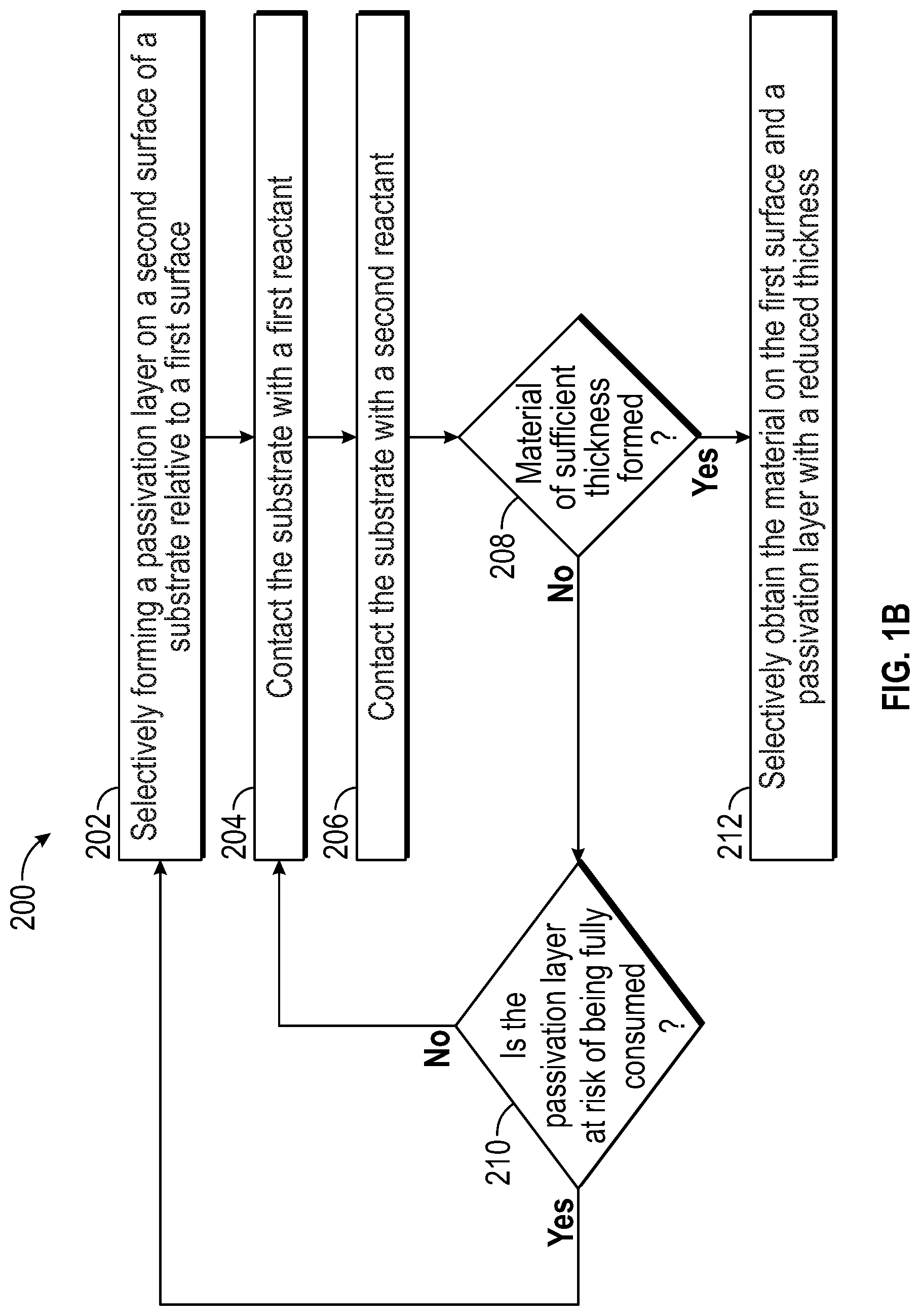
The thickness of the oxide film that can be formed on dielectric surface before the passivation layer is completely removed depends on the passivation layer initial thickness, ash rate of the passivation layer, and the growth rate of the oxide deposition process. For example, FIG. 2 demonstrates that with an ash rate of .about.0.2 .ANG./cycle, a 20 nm sacrificial polyimide layer on a metal surface, and a growth per cycle (GPC) of 1 .ANG./cycle, 50 nm of SiO.sub.2 may be deposited on a dielectric surface by applying 500 cycles of the oxygen based PEALD process. FIG. 2 shows the ash rate of polyimide when exposed to oxidant phases in which argon is supplied at 700 sccm, O.sub.2 is supplied at 100 sccm, pressure is kept at 2 Torr, plasma power is set to 100 W, substrate temperature is maintained at 100.degree. C., and each oxidant phase includes 1 second of O.sub.2 plasma and 1 second of purge. The PEALD would include one phase of the above oxidant phase alternated with supply of a silicon precursor and purge, where the silicon precursor is selected for adsorption on the dielectric or growing silicon oxide film and to react with the oxidant phases to form silicon oxide. In other embodiments, oxidant phases can be alternated with a supply of one or more metal precursor phase(s) and attendant purge phase(s), where the metal precursor is selected to adsorb on the dielectric surface or the growing metal oxide film and to react to with the oxidant phases to form the desired oxide.
In some embodiments, optimization of the etch rate of the sacrificial passivation layer can be tuned so that growth of the oxide material film or dielectric film does not result in net deposition on the passivation layer during the ALD process. In some embodiments, the incubation time for deposition on the passivation layer is sufficiently long enough that a desired oxide layer thickness is deposited on the dielectric surface. In some embodiments a thick enough passivation layer is formed over the metal surface such that a sufficiently thick oxide film may be deposited over the dielectric surface using the ALD process without further depositing another passivation film layer, i.e., without fully consuming the initial passivation layer.
In some embodiments, a selective passivation layer deposition and the selective ALD process are performed in an iterative manner, for example such using the process described in FIG. 1B. This iterative process may enable the thickness of the passivation layer to be replenished after the ALD process is performed, therefore allowing subsequent ALD processes to be performed. For example, if the passivation layer is ashed away in 100 cycles or if the incubation on passivation layer is 100 cycles before the deposited oxide begins to form on the passivation layer faster than it can be removed by undercutting, 90 cycles of a first ALD process may be performed to selectively deposit the oxide on the dielectric surface, deposition of a subsequent passivation layer over the previous passivation layer may be performed, and a second 90 cycles of the ALD process may be performed. In some embodiments, this iterative process may be repeated as many times as desired to obtain a desired oxide layer thickness on the dielectric surface. A person of ordinary skill in the art would appreciate that the number of iterative processes necessary would vary depending on a number of factors such as, for example, the thickness of the deposited oxide desired, the thickness of the passivation layer, and the ash rate or incubation period of the passivation layer.
In some embodiments, the PEALD deposition may be carried out essentially as described above. In other embodiments, the substrate is alternately and sequentially contacted with a first reactant comprising elements to be included in the deposited material, such as a metal or silicon, and a second reactant comprising oxygen, and a second plasma reactant. In some embodiments the second plasma reactant does not comprise oxygen species. In some embodiments no reactants comprising oxygen species are used other than the second reactant. The plasma and precursors (i.e. the first and second reactants) may be provided in pulses separated by a removal process (e.g., purge) in which excess reactant and reaction byproducts, if any, are removed from the reaction space. In some embodiments, a PEALD deposition process begins with the plasma pulse followed by the precursors, and the reaction sequence, or deposition cycle, may be repeated a desired number of times (A):
A.times.(plasma pulse/purge/precursors/purge)
In some embodiments the deposition cycle begins with the non-plasma precursors, which is then followed by the plasma pulse.
According to some embodiments, PEALD processes utilized may be any suitable oxygen based plasma processes. In some embodiments, the deposited dielectric film is an oxide film. In some embodiments, the deposited dielectric film is a metal oxide film. In some embodiments, the deposited dielectric film may be selected from the group consisting of SiO.sub.2, TiO.sub.2, ZrO.sub.2, HfO.sub.2, Nb.sub.2O.sub.5, Ta.sub.2O.sub.5, WO.sub.3 and NiO. In some embodiments, the deposited dielectric film is silicon oxide. In some embodiments, an oxide precursor is an alkylaminosilane, which is used to deposit silicon oxide films.
In some embodiments, an oxide film is selectively formed on a first dielectric surface of a substrate relative to a second, different metal or metallic surface of the substrate by an oxygen-based PEALD process. For example, silicon oxide may be selectively deposited by oxygen-based PEALD on a low-k dielectric surface (e.g., silicon oxide-based surface) relative to a metal surface.
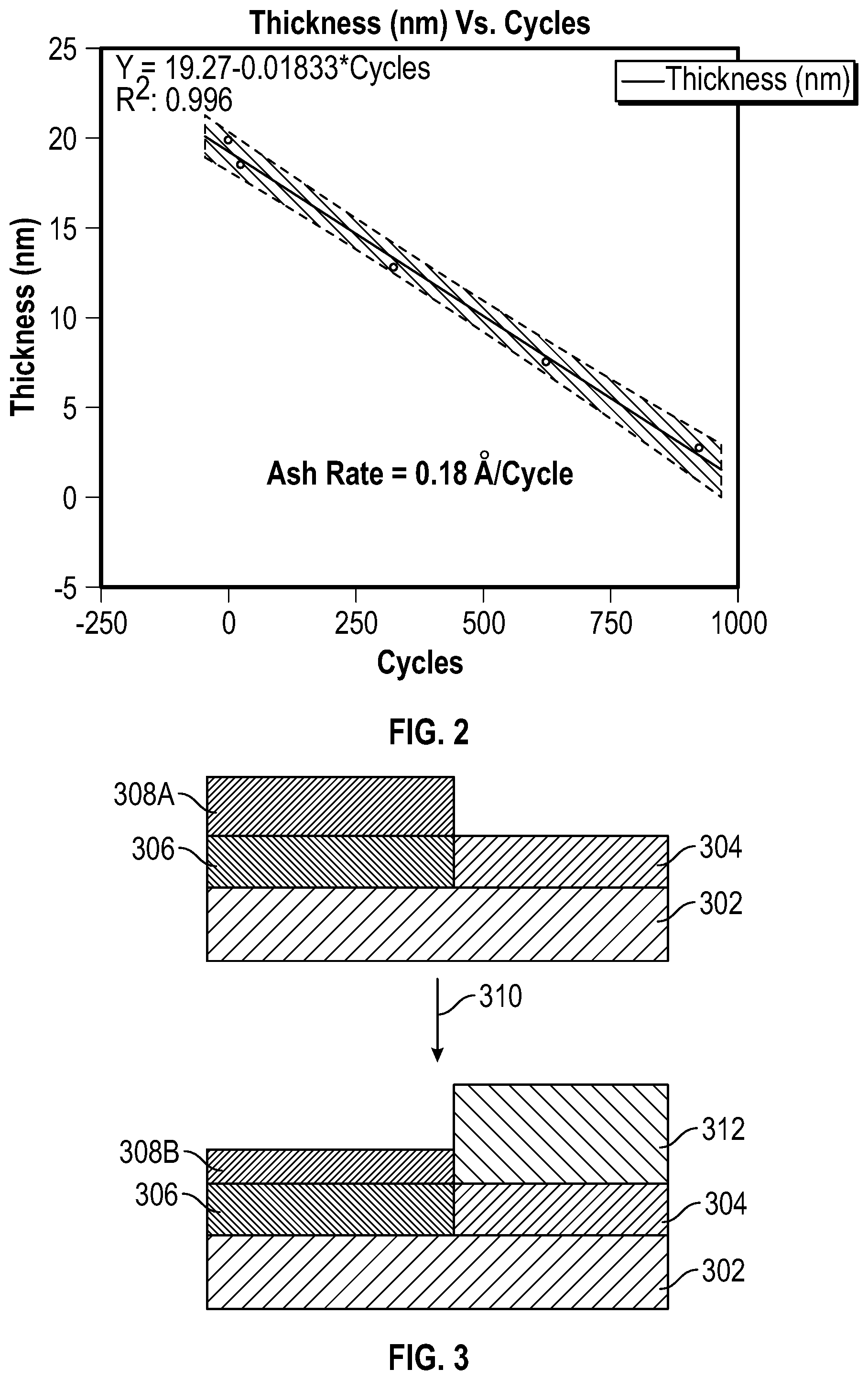
FIG. 3 shows a schematic of some embodiments, wherein a substrate 302 comprises a first surface of a first structure 304 (for example, a dielectric surface of a dielectric layer) and a second surface of a second structure 306 that has a different material composition (for example, a metal surface of a metal layer, such as a cobalt, copper or tungsten surface) further comprising an initial passivation layer 308A having a first thickness (for example, 20 nm of a polyimide organic layer), in which a material 312 is selectively deposited on the first surface relative to the second surface (due to selectively relative to the overlying initial passivation layer 308A). In some embodiments the selectively deposited material 312 is an oxide material. In some embodiments, the oxide material is a dielectric material. In examples described herein, the dielectric oxide is a film of silicon oxide. As can be seen in FIG. 3, after one or more cycles of a selective deposition process 310 (for example, 500 cycles of an oxygen based PEALD silicon oxide deposition process), the material 312 (for example, 50 nm of SiO) is deposited over the first surface of the first structure 304 and the remaining passivation layer 308B has decreased to a second thickness (for example, 10 nm of a polyimide organic layer). In some embodiments, the selective deposition process halts before all of the initial passivation layer is removed. In some embodiments, after the selective deposition process is completed, the reduced thickness of the remaining passivation layer 308B may be subsequently removed (for example, by ashing) without deposition to expose the second surface of the second structure 306.
In some embodiments, the PEALD process disclosed may accomplish selective formation of silicon oxide or other oxides on dielectric surfaces. In some embodiments, the PEALD process disclosed may accomplish a reduction in the number of steps for forming desired patterns in various device manufacturing process flows, relative to convention patterning processes.
It will be understood by those of skill in the art that numerous and various modifications can be made without departing from the spirit of the present invention. The described features, structures, characteristics and precursors can be combined in any suitable manner. Therefore, it should be clearly understood that the forms of the present invention are illustrative only and are not intended to limit the scope of the present invention. All modifications and changes are intended to fall within the scope of the invention, as defined by the appended claims.
* * * * *
D00000
D00001
D00002
D00003
XML
uspto.report is an independent third-party trademark research tool that is not affiliated, endorsed, or sponsored by the United States Patent and Trademark Office (USPTO) or any other governmental organization. The information provided by uspto.report is based on publicly available data at the time of writing and is intended for informational purposes only.
While we strive to provide accurate and up-to-date information, we do not guarantee the accuracy, completeness, reliability, or suitability of the information displayed on this site. The use of this site is at your own risk. Any reliance you place on such information is therefore strictly at your own risk.
All official trademark data, including owner information, should be verified by visiting the official USPTO website at www.uspto.gov. This site is not intended to replace professional legal advice and should not be used as a substitute for consulting with a legal professional who is knowledgeable about trademark law.