Selective deposition of aluminum and nitrogen containing material
Wang , et al. Feb
U.S. patent number 10,566,185 [Application Number 14/819,274] was granted by the patent office on 2020-02-18 for selective deposition of aluminum and nitrogen containing material. This patent grant is currently assigned to ASM IP Holding B.V.. The grantee listed for this patent is ASM IP Holding B.V.. Invention is credited to Timo Asikainen, David de Roest, Julian Hsieh, Delphine Longrie, Jan Willem Maes, Han Wang, Qi Xie, Chiyu Zhu.


| United States Patent | 10,566,185 |
| Wang , et al. | February 18, 2020 |
Selective deposition of aluminum and nitrogen containing material
Abstract
Methods are provided for selectively depositing Al and N containing material on a first conductive surface of a substrate relative to a second, dielectric surface of the same substrate. In some aspects, methods of forming an Al and N containing protective layer or etch stop layer for use in integrated circuit fabrication are provided.
| Inventors: | Wang; Han (Leuven, BE), Xie; Qi (Leuven, BE), Longrie; Delphine (Ghent, BE), Maes; Jan Willem (Wilrijk, BE), de Roest; David (Kessel-Lo, BE), Hsieh; Julian (Zhubei, TW), Zhu; Chiyu (Helsinki, FI), Asikainen; Timo (Helsinki, FI) | ||||||||||
|---|---|---|---|---|---|---|---|---|---|---|---|
| Applicant: |
|
||||||||||
| Assignee: | ASM IP Holding B.V. (Almere,
NL) |
||||||||||
| Family ID: | 58053516 | ||||||||||
| Appl. No.: | 14/819,274 | ||||||||||
| Filed: | August 5, 2015 |
Prior Publication Data
| Document Identifier | Publication Date | |
|---|---|---|
| US 20170040164 A1 | Feb 9, 2017 | |
| Current U.S. Class: | 1/1 |
| Current CPC Class: | H01L 21/76897 (20130101); H01L 21/0228 (20130101); H01L 21/02315 (20130101); H01L 21/76834 (20130101); H01L 21/02178 (20130101); H01L 21/31111 (20130101); H01L 21/31144 (20130101); H01L 21/283 (20130101); H01L 21/02205 (20130101) |
| Current International Class: | H01L 21/02 (20060101); H01L 21/283 (20060101); H01L 21/311 (20060101) |
References Cited [Referenced By]
U.S. Patent Documents
| 4804640 | February 1989 | Kaganowicz |
| 4863879 | September 1989 | Kwok |
| 4948755 | August 1990 | Mo |
| 5288697 | February 1994 | Schrepp et al. |
| 5447887 | September 1995 | Filipiak et al. |
| 5604153 | February 1997 | Tsubouchi et al. |
| 5633036 | May 1997 | Seebauer et al. |
| 5869135 | February 1999 | Vaeth et al. |
| 5925494 | July 1999 | Horn |
| 6046108 | April 2000 | Liu et al. |
| 6482740 | November 2002 | Soininen et al. |
| 6586330 | July 2003 | Ludviksson et al. |
| 6679951 | January 2004 | Soininen et al. |
| 6759325 | July 2004 | Raaijmakers et al. |
| 6811448 | November 2004 | Paton |
| 6844258 | January 2005 | Fair et al. |
| 6878628 | April 2005 | Sophie et al. |
| 6887795 | May 2005 | Soininen et al. |
| 6921712 | July 2005 | Soininen et al. |
| 6958174 | October 2005 | Klaus et al. |
| 7067407 | June 2006 | Kostamo et al. |
| 7084060 | August 2006 | Furukawa et al. |
| 7118779 | October 2006 | Verghese et al. |
| 7220669 | May 2007 | Hujanen et al. |
| 7241677 | July 2007 | Soininen et al. |
| 7323411 | January 2008 | Blosse |
| 7405143 | July 2008 | Leinikka et al. |
| 7425350 | September 2008 | Todd |
| 7476618 | January 2009 | Kilpela et al. |
| 7494927 | February 2009 | Kostamo et al. |
| 7595271 | September 2009 | White |
| 7754621 | July 2010 | Putkonen |
| 7790631 | September 2010 | Sharma et al. |
| 7799135 | September 2010 | Verghese et al. |
| 7910177 | March 2011 | Li |
| 7914847 | March 2011 | Verghese et al. |
| 7927942 | April 2011 | Raaijmakers |
| 7955979 | June 2011 | Kostamo et al. |
| 7964505 | June 2011 | Khandelwal et al. |
| 8293597 | October 2012 | Raaijmakers |
| 8293658 | October 2012 | Shero et al. |
| 8425739 | April 2013 | Wieting |
| 8536058 | September 2013 | Kostamo et al. |
| 8778815 | July 2014 | Yamaguchi et al. |
| 8890264 | November 2014 | Dewey et al. |
| 8956971 | February 2015 | Haukka et al. |
| 8962482 | February 2015 | Albertson et al. |
| 8980418 | March 2015 | Darling et al. |
| 8993404 | March 2015 | Kobrinsky et al. |
| 9067958 | June 2015 | Romero |
| 9112003 | August 2015 | Haukka et al. |
| 9129897 | September 2015 | Pore et al. |
| 9136110 | September 2015 | Rathsack |
| 9159558 | October 2015 | Cheng et al. |
| 9236292 | January 2016 | Romero et al. |
| 9257303 | February 2016 | Haukka et al. |
| 9349687 | May 2016 | Gates et al. |
| 9490145 | November 2016 | Niskanen et al. |
| 9502289 | November 2016 | Haukka et al. |
| 9803277 | October 2017 | Longrie et al. |
| 9895715 | February 2018 | Haukka et al. |
| 9911595 | March 2018 | Smith et al. |
| 10041166 | August 2018 | Longrie et al. |
| 2001/0019803 | September 2001 | Mirkanimi |
| 2001/0025205 | September 2001 | Chern et al. |
| 2002/0027261 | March 2002 | Blesser et al. |
| 2002/0047144 | April 2002 | Nguyen et al. |
| 2002/0068458 | June 2002 | Chiang et al. |
| 2002/0090777 | July 2002 | Forbes |
| 2002/0107316 | August 2002 | Bice et al. |
| 2003/0027431 | February 2003 | Sneh et al. |
| 2003/0066487 | April 2003 | Suzuki |
| 2003/0143839 | July 2003 | Raaijmakers et al. |
| 2003/0181035 | September 2003 | Yoon et al. |
| 2003/0192090 | October 2003 | Meilland |
| 2003/0193090 | October 2003 | Otani et al. |
| 2004/0092073 | May 2004 | Cabral |
| 2004/0219746 | November 2004 | Vaartstra et al. |
| 2005/0012975 | January 2005 | George et al. |
| 2005/0136604 | June 2005 | Al-Bayati et al. |
| 2005/0223989 | October 2005 | Lee et al. |
| 2006/0019493 | January 2006 | Li |
| 2006/0047132 | March 2006 | Shenai-Khatkhate |
| 2006/0121271 | June 2006 | Frey et al. |
| 2006/0141155 | June 2006 | Gordon et al. |
| 2006/0176559 | August 2006 | Takatoshi et al. |
| 2006/0199399 | September 2006 | Muscat |
| 2006/0226409 | October 2006 | Burr et al. |
| 2006/0292845 | December 2006 | Chiang et al. |
| 2007/0014919 | January 2007 | Hamalainen et al. |
| 2007/0026654 | February 2007 | Huotari et al. |
| 2007/0063317 | March 2007 | Kim et al. |
| 2007/0099422 | May 2007 | Wijekoon et al. |
| 2007/0241390 | October 2007 | Tanaka et al. |
| 2007/0292604 | December 2007 | Dordi et al. |
| 2008/0066680 | March 2008 | Sherman |
| 2008/0072819 | March 2008 | Rahtu |
| 2008/0124932 | May 2008 | Tateishi et al. |
| 2008/0179741 | July 2008 | Streck |
| 2008/0241575 | October 2008 | Lavoie et al. |
| 2008/0282970 | November 2008 | Heys et al. |
| 2009/0035949 | February 2009 | Niinisto et al. |
| 2009/0071505 | March 2009 | Miya et al. |
| 2009/0081385 | March 2009 | Heys et al. |
| 2009/0203222 | August 2009 | Dussarrat et al. |
| 2009/0269507 | October 2009 | Yu et al. |
| 2009/0274887 | November 2009 | Millward et al. |
| 2009/0311879 | December 2009 | Blasco et al. |
| 2010/0015756 | January 2010 | Weidman et al. |
| 2010/0147396 | June 2010 | Yamagishi et al. |
| 2010/0248473 | September 2010 | Ishizaka et al. |
| 2010/0270626 | October 2010 | Raisanen |
| 2010/0297474 | November 2010 | Dameron |
| 2011/0053800 | March 2011 | Jung et al. |
| 2011/0124192 | May 2011 | Ganguli et al. |
| 2011/0146568 | June 2011 | Haukka et al. |
| 2011/0221061 | September 2011 | Prakash et al. |
| 2011/0311726 | December 2011 | Liu et al. |
| 2012/0032311 | February 2012 | Gates |
| 2012/0046421 | February 2012 | Darling et al. |
| 2012/0052681 | March 2012 | Marsh |
| 2012/0088369 | April 2012 | Weidman et al. |
| 2012/0189868 | July 2012 | Borovik et al. |
| 2012/0219824 | August 2012 | Prolier et al. |
| 2012/0264291 | October 2012 | Ganguli et al. |
| 2012/0269970 | October 2012 | Ido et al. |
| 2013/0005133 | January 2013 | Lee et al. |
| 2013/0078793 | March 2013 | Sun et al. |
| 2013/0089983 | April 2013 | Sugita et al. |
| 2013/0095664 | April 2013 | Matero et al. |
| 2013/0115768 | May 2013 | Pore et al. |
| 2013/0126815 | May 2013 | Kim |
| 2013/0146881 | June 2013 | Yamazaki et al. |
| 2013/0189837 | July 2013 | Haukka et al. |
| 2013/0196502 | August 2013 | Haukka et al. |
| 2013/0203267 | August 2013 | Pomarede et al. |
| 2013/0280919 | October 2013 | Yuasa et al. |
| 2013/0284094 | October 2013 | Pavol et al. |
| 2013/0316080 | November 2013 | Yamaguchi et al. |
| 2013/0323930 | December 2013 | Chattopadhyay et al. |
| 2014/0001572 | January 2014 | Bohr et al. |
| 2014/0024200 | January 2014 | Kato et al. |
| 2014/0091308 | April 2014 | Dasgupta et al. |
| 2014/0120738 | May 2014 | Jung et al. |
| 2014/0152383 | June 2014 | Nikonov et al. |
| 2014/0190409 | July 2014 | Matsumoto et al. |
| 2014/0193598 | July 2014 | Traser et al. |
| 2014/0205766 | July 2014 | Lyon et al. |
| 2014/0209022 | July 2014 | Inoue et al. |
| 2014/0227461 | August 2014 | Darwish et al. |
| 2014/0273290 | September 2014 | Somervell |
| 2014/0273514 | September 2014 | Somervell et al. |
| 2014/0273523 | September 2014 | Rathsack |
| 2014/0273527 | September 2014 | Niskanen et al. |
| 2015/0004806 | January 2015 | Ndiege et al. |
| 2015/0011032 | January 2015 | Kunimatsu et al. |
| 2015/0011093 | January 2015 | Singh et al. |
| 2015/0037972 | February 2015 | Danek et al. |
| 2015/0064931 | March 2015 | Kumagi et al. |
| 2015/0083415 | March 2015 | Monroe et al. |
| 2015/0087158 | March 2015 | Sugita et al. |
| 2015/0093890 | April 2015 | Blackwell et al. |
| 2015/0097292 | April 2015 | He et al. |
| 2015/0118863 | April 2015 | Rathod et al. |
| 2015/0162214 | June 2015 | Thompson et al. |
| 2015/0170961 | June 2015 | Romero et al. |
| 2015/0179798 | June 2015 | Clendenning et al. |
| 2015/0217330 | August 2015 | Haukka et al. |
| 2015/0240121 | August 2015 | Sugita et al. |
| 2015/0299848 | October 2015 | Haukka et al. |
| 2015/0371866 | December 2015 | Chen et al. |
| 2015/0376211 | December 2015 | Girard et al. |
| 2016/0075884 | March 2016 | Chen |
| 2016/0079524 | March 2016 | Do |
| 2016/0186004 | June 2016 | Hustad et al. |
| 2016/0190060 | June 2016 | Bristol et al. |
| 2016/0222504 | August 2016 | Haukka et al. |
| 2016/0247695 | August 2016 | Niskanen et al. |
| 2016/0276208 | September 2016 | Haukka et al. |
| 2016/0293398 | October 2016 | Danek et al. |
| 2016/0346838 | December 2016 | Fujita et al. |
| 2016/0365280 | December 2016 | Brink et al. |
| 2017/0037513 | February 2017 | Haukka et al. |
| 2017/0040164 | February 2017 | Wang et al. |
| 2017/0058401 | March 2017 | Blackwell et al. |
| 2017/0069527 | March 2017 | Haukka et al. |
| 2017/0100742 | April 2017 | Pore et al. |
| 2017/0100743 | April 2017 | Pore et al. |
| 2017/0107413 | April 2017 | Wang et al. |
| 2017/0154806 | June 2017 | Wang et al. |
| 2017/0298503 | October 2017 | Maes et al. |
| 2017/0301542 | October 2017 | Maes et al. |
| 2017/0323776 | November 2017 | Farm et al. |
| 2017/0352533 | December 2017 | Tois et al. |
| 2017/0352550 | December 2017 | Tois et al. |
| 2019/0017170 | January 2019 | Sharma et al. |
| 2019/0057858 | February 2019 | Hausmann et al. |
| 2019/0074441 | March 2019 | Kikuchi et al. |
| 0469456 | Feb 1992 | EP | |||
| 0880168 | Nov 1998 | EP | |||
| 1340269 | Feb 2009 | EP | |||
| 4333900 | Sep 2009 | JP | |||
| 2011-187583 | Sep 2011 | JP | |||
| 2014-93331 | May 2014 | JP | |||
| 102001001072 | Feb 2001 | KR | |||
| 20030027392 | Apr 2003 | KR | |||
| 1020040056026 | Jun 2004 | KR | |||
| 10-0869326 | Nov 2008 | KR | |||
| 10-2012-0120902 | Nov 2012 | KR | |||
| 175767 | Aug 2003 | TW | |||
| WO 2002/045167 | Jun 2002 | WO | |||
| WO 2011/156705 | Dec 2011 | WO | |||
| WO 2013/161772 | Oct 2013 | WO | |||
| WO 2014/156782 | Oct 2014 | WO | |||
| WO 2014209390 | Dec 2014 | WO | |||
| WO 2015/047345 | Apr 2015 | WO | |||
| WO 2015094305 | Jun 2015 | WO | |||
| WO 2015147843 | Oct 2015 | WO | |||
| WO 2015147858 | Oct 2015 | WO | |||
| WO 2017/184357 | Oct 2017 | WO | |||
| WO 2017/184358 | Oct 2017 | WO | |||
Other References
|
Senesky et al., "Aluminum nitride as a masking material for the plasma etching of silicon carbide structures," 2010, IEEE, pp. 352-355. cited by examiner . Vallat et al., Selective deposition of Ta2O5 by adding plasma etching super-cycles in plasma enhanced atomic layer deposition steps, Journal of Vacuum Science & Technology A, vol. 35, No. 1, pp. 01B104-1-01B104-7, Jan. 2017. cited by applicant . Burton, B.B. et al., "Atomic Layer Deposition of MgO Using Bis(ethylcyclopentadienyl)magnesium and H2O". J. Phys. Chem. C, 2009, 113, 1939-1946. cited by applicant . Burton, B.B., et al. "SiO2 Atomic Layer Deposition Using Tris(dimethylamino)silane and Hydrogen Peroxide Studied by in Situ Transmission FTIR Spectroscopy". J. Phys. Chem. C, 2009, 113, 8249-8257. cited by applicant . Liang, Xuehai, et al., "Growth of Ge Nanofilms Using Electrochemical Atomic Layer Deposition, with a "Bait and Switch" Surface-Limited Reaction". Journal of American Chemical Society, 2011, 133, 8199-8024. cited by applicant . Overhage et al., Selective Atomic Layer Deposition (SALD) of Titanium Dioxide on Silicon and Copper Patterned Substrates, Journal of Undergraduate Research 4, 29, Mar. 2011 in 4 pages. cited by applicant . Chen et al., Highly Stable Monolayer Resists for Atomic Layer Deposition on Germanium and Silicon, Chem. Matter, vol. 18, No. 16, pp. 3733-3741, 2006. cited by applicant . Ghosal et al., Controlling Atomic Layer Deposition of TiO2 in Aerogels through Surface Functionalization, Chem. Matter, vol. 21, pp. 1989-1992, 2009. cited by applicant . King, Dielectric Barrier, Etch Stop, and Metal Capping Materials for State of the Art and beyond Metal Interconnects, ECS Journal of Solid State Science and Technology, vol. 4, Issue 1, pp. N3029-N3047, 2015. cited by applicant . Lee et al., Area-Selective Atomic Layor Deposition Using Self-Assembled Monolayer and Scanning Probe Lithography, Journal of the Electrochemical Society, vol. 156, Issue 9, pp. G125-G128, 2009. cited by applicant . Low et al., Selective deposition of CVD iron on silicon dioxide and tungsten, Microelectronic Engineering 83, pp. 2229-2233, 2006. cited by applicant . Mackus et al., Influence of Oxygen Exposure on the Nucleation of Platinum Atomic Layer Deposition: Consequences for Film Growth, Nanopatterning, and Nanoparticle Synthesis, Chem. Matter, vol. 25, pp. 1905-1911, 2013. cited by applicant . Mackus et al., Local deposition of high-purity Pt nanostructures by combining electron beam induced deposition and atomic layer deposition, Journal of Applied Physics, vol. 107, pp. 116102-1-116102-3, 2010. cited by applicant . Parulekar et al., Atomic Layer Deposition of Zirconium Oxide on Copper Patterned Silicon Substrate, Journal of Undergraduate Research, vol. 7, pp. 15-17, 2014. cited by applicant . Parulekar et al., Selective atomic layer deposition of zirconium oxide on copper patterned silicon substrate, pp. 1-6, 2013. cited by applicant . Schmei er, Decomposition of formic acid, Chemnitz University of Technology, pp. 1-13, Aug. 31, 2011. cited by applicant . Schmei er, Reduction of Copper Oxide by Formic Acid an ab-initio study, Chemnitz University of Technology, pp. 1-42, Sep. 2011. cited by applicant . Selvaraj et al., Selective atomic layer deposition of zirconia on copper patterned silicon substrates using ethanol as oxygen source as well as copper reductant, Journal of Vacuum Science & Technology A, vol. 32, No. 1, pp. 010601-1-010601-4, Jan. 2014. cited by applicant . Bernal-Ramos, et al., "Atomic Layer Deposition of Cobalt Silicide Thin Films Studied by in Situ Infrared Spectroscopy", Chem. Mater. 2015, 27, pp. 4943-4949. cited by applicant . Lemonds, A.M., "Atomic layer deposition of TaSi.sub.x thin films on SiO.sub.2 using TaF.sub.5 and Si.sub.2H.sub.6", Thin Solid Films, 488, 2005 pp. 9-14. cited by applicant . Ellinger et al., "Selective Area Spatial Atomic Layer Deposition of ZnO, Al.sub.2O.sub.3, and Aluminum-Doped ZnO Using Poly(vinyl pyrrolidone)", Chem. Mater. 2014, 26, pp. 1514-1522. cited by applicant . File History of U.S. Appl. No. 15/177,195, filed Jun. 8, 2016. cited by applicant . File History of U.S. Appl. No. 13/708,863, filed Dec. 7, 2012. cited by applicant . Vervuurt et al., "Area-selective atomic layer deposition of platinum using photosensitive polyimide", Nanotechnology 27, 2016, in 6 pages. cited by applicant . Aaltonen et al., "Atomic Layer Deposition of Iridium Thin Films", Journal of the Electrochemical Society, 151 (8) G489-G492 (2004). cited by applicant . Au et al., "Selective Chemical Vapor Deposition of Manganese Self-Aligned Capping Layer for Cu Interconnections in Microelectronics", Journal of the Electrochemical Society, vol. 157, No. 6, 2010, pp. D341-D345. cited by applicant . Benzotriazole, Wikipedia via https://en.wikipedia.org/wiki/Benzotriazole; pp. 1-5, no date available. cited by applicant . Bouteville et al., "Selective R.T.L.P.C.V.D. of Tungsten by Silane Reduction on Patterned PPQ/Si Wafers" Journal De Physique IV, Colloque C2, suppl. au Journal de Physique II, vol. 1, Sep. 1991, pp. C2-857-C2-864. cited by applicant . Carlsson, J., "Precursor Design for Chemical Vapour Deposition", Acta Chemica Scandinavica, vol. 45, 1991, pp. 864-869. cited by applicant . Chang et al, "Influences of damage and contamination from reactive ion etching on selective tungsten deposition in a low-pressure chemical-vapor-deposition reactor", J. Appl. Phys., vol. 80, No. 5, Sep. 1, 1996, pp. 3056-3061. cited by applicant . Coclite, et al.; 25th Anniversary Article: CVD Polymers: A New Paradigm for Surface Modification and Device Fabrication; Advanced Materials; Oct. 2013; 25; pp. 5392-5423. cited by applicant . Elam et al., "Kinetics of the WF6 and Si2H6 surface reactions during tungsten atomic layer deposition", Surface Science, vol. 479, 2001, pp. 121-135. cited by applicant . Elam et al., "Nucleation and growth during tungsten atomic layer deposition on SiO2 surfaces", Thin Solid Films, vol. 386, 2001 pp. 41-52. cited by applicant . Fabreguette et al., Quartz crystal microbalance study of tungsten atomic layer deposition using WF6 and Si2H6, Thin Solid Films, vol. 488, 2005, pp. 103-110. cited by applicant . Farm et al. Selective-Area Atomic Layer Deposition Using Poly( methyl methacrylate) Films as Mask Layers, J. Phys. Chem. C, 2008, 112, pp. 15791-15795. (Year: 2008). cited by applicant . Farm et al., "Self-Assembled Octadecyltrimethoxysilane Monolayers Enabling Selective-Area Atomic Layer Deposition of Iridium", Chem. Vap. Deposition, 2006, 12, pp. 415-417. cited by applicant . Farr, Isaac Vincent; Synthesis and Characterization of Novel Polyimide Gas Separation Membrane Material Systems, Chapter 2; Virginia Tech Chemistry PhD Dissertation; URN# etd-080999-123034; Jul. 26, 1999. cited by applicant . File History of U.S. Appl. No. 14/612,784, filed Feb. 3, 2015. cited by applicant . File History of U.S. Appl. No. 15/877,632, filed Jan. 23, 2018. cited by applicant . File History of U.S. Appl. No. 14/687,833, filed Apr. 15, 2015. cited by applicant . File History of U.S. Appl. No. 16/100,855, filed Aug. 10, 2018. cited by applicant . File History of U.S. Appl. No. 14/628,799, filed Feb. 23, 2015. cited by applicant . File History of U.S. Appl. No. 15/331,366, filed Oct. 21, 2016. cited by applicant . File History of U.S. Appl. No. 16/143,888, filed Sep. 27, 2018. cited by applicant . File History of U.S. Appl. No. 14/817,161, filed Aug. 3, 2015. cited by applicant . File History of U.S. Appl. No. 15/432,263, filed Feb. 14, 2017. cited by applicant . File History of U.S. Appl. No. 16/158,780, filed Oct. 12, 2018. cited by applicant . File History of U.S. Appl. No. 15/221,453, filed Jul. 27, 2016. cited by applicant . File History of U.S. Appl. No. 15/795,768, filed Oct. 27, 2017. cited by applicant . File History of U.S. Appl. No. 16/040,844, filed Jul. 20, 2018. cited by applicant . File History of U.S. Appl. No. 15/581,726, filed Apr. 28, 2017. cited by applicant . File History of U.S. Appl. No. 15/364,024, filed Nov. 29, 2016. cited by applicant . File History of U.S. Appl. No. 15/892,728, filed Feb. 9, 2018. cited by applicant . File History of U.S. Appl. No. 15/356,306, filed Nov. 18, 2016. cited by applicant . File History of U.S. Appl. No. 16/213,479, filed Dec. 7, 2018. cited by applicant . File History of U.S. Appl. No. 13/702,992, filed Mar. 26, 2013. cited by applicant . File History of U.S. Appl. No. 14/613,183, filed Feb. 3, 2015. cited by applicant . File History of U.S. Appl. No. 14/988,374, filed Jan. 5, 2016. cited by applicant . File History of U.S. Appl. No. 15/609,497, filed May 31, 2017. cited by applicant . File History of U.S. Appl. No. 16/100,581, filed Aug. 10, 2018. cited by applicant . Formic Acid, Wikipedia via https://en.wikipedia.org/wiki/Formic_acid; pp. 1-5, no date available. cited by applicant . George, Steven M., "Atomic Layer Deposition: An Overview", Chem. Rev. 2010, 110, pp. 111-113. cited by applicant . Grubbs et al., "Nucleation and growth during the atomic layer deposition of W on Al2O3 and Al2O3 on W", Thin Solid Films, vol. 467, 2004, pp. 16-27. cited by applicant . Hashemi et al., "A New Resist for Area Selective Atomic and Molecular Layer Deposition on Metal-Dielectric Patterns", J. Phys. Chem. C 2014, 118, pp. 10957-10962. cited by applicant . Hashemi et al., "Selective Deposition of Dieletrics: Limits and Advantages of Alkanethiol Blocking Agents on Metal-Dielectric Patterns", ACS Appl. Mater. Interfaces 2016, 8, pp. 33264-33272. cited by applicant . Hymes et al., "Surface cleaning of copper by thermal and plasma treatment in reducing and inert ambients", J. Vac. Sci. Technol. B, vol. 16, No. 3, May/Jun. 1998, pp. 1107-1109. cited by applicant . International Search Report and Written Opinion dated Feb. 17, 2012 in Application No. PCT/US2011/039970, filed Jun. 10, 2011. cited by applicant . Klaus et al., "Atomic layer deposition of tungsten using sequential surface chemistry with a sacrificial stripping reaction", Thin Solid Films, vol. 360, 2000, pp. 145-153. cited by applicant . Klaus et al., "Atomically controlled growth of tungsten and tungsten nitride using sequential surface reactions", Applied Surface Science 162-163, 2000, pp. 479-491. cited by applicant . Kukli et al., "Properties of hafnium oxide films grown by atomic layer deposition from hafnium tetraiodide and oxygen", J. Appl. Phys., vol. 92, No. 10, Nov. 15, 2002, pp. 5698-5703. cited by applicant . Lecordier et al., "Vapor-deposited octadecanethlol masking layer on copper to enable area selective Hf3N4 atomic layer deposition on dielectrics studied by in situ spectroscopic ellipsometry", J. Vac. Sci. Technol. A36(3), May/Jun. 2018, pp. 031605-1-031605-8. cited by applicant . Lei et al., "Real-time observation and opitimization of tungsten atomic layer deposition process cycle", J. Vac. Sci. Technol. B, vol. 24, No. 2, Mar./Apr. 2006, pp. 780-789. cited by applicant . Lemonds, Andrew Michael, "Atomic Layer Deposition and Properties of Refractory Transition Metal-Based Copper-Diffusion Barriers for ULSI Interconnect", The University of Texas at Austin, 2003, pp. 1-197. cited by applicant . Leusink et al., "Growth kinetics and inhibition of growth of chemical vapor deposited thin tungsten films on silicon from tungsten hexafluoride", J. Appl. Phys., vol. 72, No. 2, Jul. 15, 1992, pp. 490-498. cited by applicant . Lohokare et al., "Reactions of Disilane on Cu(111): Direct Observation of Competitive Dissociation, Disproportionation, and Thin Film Growth Processes", Langmuir 1995, vol. 11, pp. 3902-3912. cited by applicant . Mackus et al., "The use of atomic layer deposition in advanced nanopatterning", Nanoscale, 2014, 6, pp. 10941-10960. cited by applicant . Maluf et al., "Selective tungsten filling of sub-0.25.mu.m trenches for the fabrication of scaled contacts and x-ray masks", J. Vac. Sci. Technol. B, vol. 8, No. 3, May/Jun. 1990, pp. 568-569. cited by applicant . Norrman, et al.; 6 Studies of Spin-Coated Polymer Films; Annu. Rep. Prag. Chem.; Sect. C; 2005; 101; pp. 174-201. cited by applicant . Office Action dated Jun. 8, 2017 in Korean Application No. 2013-7000596. cited by applicant . Prasittichai et al., "Area Selective Molecular Layer Deposition of Polyurea Film", Applied Materials & Interfaces, 2013, vol. 5, pp. 13391-13396. cited by applicant . Proslier et al., "Atomic Layer Deposition and Superconducting Properties of NbSi Films", The Journal of Physical Chemistry C, 2011, vol. 115, No. 50, pp. 1-26. cited by applicant . Putkonen, et al.; Atomic Layer Deposition of Polyimide Thin Films; Journal of Materials Chemistry; 2007, 17, pp. 664-669. cited by applicant . Ratta, Varun; Crystallization, Morphology, Thermal Stability and Adhesive Properties of Novel High Performance Semicrystalline Polyimides, Chapter 1; Virginia Tech Chemistry PhD Dissertation; URN # etd-051799-162256; Apr. 26, 1999. cited by applicant . Roberts et al., "Selective Mn deposition on Cu lines", poster presentation, 12th International Conference on Atomic Layer Deposition, Jun. 19, 2012, Dresden, Germany. cited by applicant . Sapp, et al.; Thermo-Mechanical and Electrical Characterization of Through-Silicon Vias with a Vapor Deposited Polyimide Dielectric Liner; IEEE; 2012. cited by applicant . Schuiskly et al., "Atomic Layer Deposition of Thin Films Using O2 as Oxygen Source", Langmuir, vol. 17, No. 18, 2001, pp. 5508-5512. cited by applicant . Sundberg, et al.; Organic and Inorganic-Organic Thin Film Structures by Molecular Layer Deposition: A Review; Beilstein J. Nanotechnol; 2014, 5, pp. 1104-1136. cited by applicant . Suntola, Tuomo, "Thin Films and Epitaxy Part B: Grown mechanism and Dynamics", Handbook of Crystal Growth vol. 3, Elsevier, 1994, 33 pages. cited by applicant . Ting, et al., "Selective Electroless Metal Deposition for Integrated Circuit Fabrication", J. Electrochem. Soc., vol. 136, No. 2, Feb. 1989, pp. 456-462. cited by applicant . Toirov, et al.; Thermal Cyclodehydration of Polyamic Acid Initiated by UV-Irradiation; Iranian Polymer Journal; vol. 5, No. 1; pp. 16-22; 1996; Iran. cited by applicant . "Tungsten and Tungsten Silicide Chemical Vapor Deposition", TimeDomain CVD, Inc., retrieved from link: http://www.timedomaincvd.com/CVD_Fundamentals/films/W_WSi.html, Last modified Jul. 11, 2008. cited by applicant . Yu et al., "Gas/surface reactions in the chemical vapor deposition of tungsten using WF6/SiH4 mixtures", J. Vac. Sci. Technol. A, vol. 7, No. 3, May/Jun. 1989, pp. 625-629. cited by applicant . Zhou, et al.; Fabrication of Organic Interfacial Layers by Molecular Layer Deposition: Present Status and Future Opportunities; Journal of Vacuum Science & Technology; A 31 (4), 040801-1 to 040801-18; 2013. cited by applicant. |
Primary Examiner: Jang; Bo B
Attorney, Agent or Firm: Knobbe, Martens, Olson & Bear LLP
Claims
What is claimed is:
1. A process for selectively depositing a material comprising aluminum and nitrogen on a first surface of a substrate relative to a second surface of the substrate comprising Si--O bonds, the process comprising two or more deposition cycles comprising: contacting the first surface and second surface of the substrate with a first precursor in the vapor phase and comprising aluminum to form no more than about one monolayer of the first precursor on the first surface of the substrate; and contacting the first surface and second surface of the substrate with a second vapor phase precursor comprising nitrogen to selectively form the material comprising aluminum and nitrogen on the first surface of the substrate relative to the second surface of the substrate; wherein the material comprising aluminum and nitrogen is selectively deposited on the first surface of the substrate relative to the second surface of the substrate with a selectivity greater than about 50% in each of the two or more deposition cycles; and the process further comprising contacting the material comprising aluminum and nitrogen with an oxygen-containing plasma after at least one deposition cycle.
2. The process of claim 1, wherein the first surface of the substrate comprises at least one of: copper, titanium nitride, tungsten, and silicon nitride.
3. The process of claim 1, wherein the material comprising aluminum and nitrogen is an aluminum nitride thin film.
4. The process of claim 3, wherein the aluminum nitride thin film comprises oxygen.
5. The process of claim 1, wherein the first precursor comprising aluminum is an organometallic aluminum compound.
6. The process of claim 1, wherein the first precursor comprising aluminum does not comprise any metals other than aluminum.
7. The process of claim 1, wherein the first precursor comprising aluminum has the formula R.sub.3Al, wherein each R can be independently selected from C.sub.1-C.sub.4 alkyl groups.
8. The process of claim 1, wherein the first precursor comprising aluminum does not comprise a halide.
9. The process of claim 1, wherein the first precursor comprising aluminum comprises one chlorine ligand and at least two alkyl ligands.
10. The process of claim 1, wherein the first precursor comprising aluminum comprises at least one hydrogen ligand and at least one alkyl ligand.
11. The process of claim 1, wherein the first precursor comprising aluminum does not comprise nitrogen, silicon, or oxygen.
12. The process of claim 1, wherein the first precursor comprising aluminum comprises tritertbutylaluminum (TTBA), trimethylaluminum (TMA) or triethylaluminum (TEA) and the second vapor phase precursor comprising nitrogen comprises NH.sub.3.
13. The process of claim 1, wherein the second surface of the substrate is a dielectric.
14. The process of claim 1, wherein the second surface of the substrate has a resistivity of more than about 1 ohmm.
15. The process of claim 1, wherein the process comprises a thermal atomic layer deposition (ALD) process.
16. The process of claim 1, wherein the process does not comprise using plasma in at least 2 consecutive deposition cycles.
17. The process of claim 1, further comprising exposing the substrate to a pretreatment reactant prior to a first deposition cycle.
18. The process of claim 17, wherein the pretreatment reactant comprises plasma.
19. The process of claim 1, wherein the material comprising aluminum and nitrogen has etch selectivity relative to SiO.sub.2 in dilute HF.
20. The process of claim 1, wherein a ratio of the material comprising aluminum and nitrogen deposited on the first surface of the substrate relative to the second surface of the substrate is greater than about 10:1, and wherein a thickness of the material comprising aluminum and nitrogen deposited on first surface of the substrate is greater than about 5 nm.
21. The process of claim 1, wherein a ratio of the material comprising aluminum and nitrogen deposited on the first surface of the substrate relative to the second surface of the substrate is greater than about 10:1 and wherein a thickness of the material comprising aluminum and nitrogen deposited on first surface of the substrate is greater than about 1 nm.
22. The process of claim 1, wherein a ratio of the material comprising aluminum and nitrogen deposited on the first surface of the substrate relative to the second surface of the substrate is greater than about 10:1 and wherein the process comprises between about 1 and 25 deposition cycles.
23. The process of claim 1, wherein a ratio of the material comprising aluminum and nitrogen deposited on the first surface of the substrate relative to the second surface of the substrate is greater than about 10:1, and wherein the process comprises between about 1 and 150 deposition cycles.
24. The process of claim 1, wherein less than about 0.1 nm of the material comprising aluminum and nitrogen is deposited on the second surface of the substrate after between about 1 and 25 deposition cycles.
25. The process of claim 1, wherein a ratio of a wet etch rate of the material comprising aluminum and nitrogen to a wet etch rate of SiO.sub.2 is less than about 1:5.
26. The process of claim 1, wherein the second surface of the substrate overlies a source/drain region, and further comprising: removing the second surface of the substrate to thereby expose the source/drain region of the substrate; and forming a contact over the exposed source/drain region of the substrate.
Description
BACKGROUND OF THE INVENTION
Field of the Invention
The present application relates to selective deposition of aluminum and nitrogen containing material, for example an Al and N containing thin film on a first surface of a substrate relative to a second surface.
Description of the Related Art
Integrated circuits are currently manufactured by an elaborate process in which various layers of materials are sequentially constructed in a predetermined arrangement on a semiconductor substrate.
The predetermined arrangement of materials on a semiconductor substrate is often accomplished by deposition of a material over the entire substrate surface, followed by removal of the material from predetermined areas of the substrate, such as by deposition of a mask layer and subsequent selective etching process.
In certain cases, the number of steps involved in manufacturing an integrated surface on a substrate may be reduced by utilizing a selective deposition process, wherein a material is selectively deposited on a first surface relative to a second surface without the need, or with reduced need for subsequent processing. Methods are disclosed herein for selective deposition on a first surface of substrate relative to a second, different surface of the substrate.
SUMMARY OF THE INVENTION
In some aspects, processes for selectively depositing a material comprising aluminum and nitrogen are provided. In some embodiments a material comprising aluminum and nitrogen is deposited on a first surface of a substrate relative to a second dielectric surface of the same substrate in a process comprising one or more deposition cycles comprising contacting the substrate with a first vapor phase precursor comprising aluminum and contacting the substrate with a second vapor phase precursor comprising nitrogen. In some embodiments a material comprising aluminum and nitrogen is deposited on a first surface of a substrate relative to a second Si--O surface of the same substrate in a process comprising one or more deposition cycles comprising contacting the substrate with a first vapor phase precursor comprising aluminum and contacting the substrate with a second vapor phase precursor comprising nitrogen. In some embodiments a material comprising aluminum and nitrogen is deposited on a first surface of a substrate relative to a second non-conductive surface of the same substrate in a process comprising one or more deposition cycles comprising contacting the substrate with a first vapor phase precursor comprising aluminum and contacting the substrate with a second vapor phase precursor comprising nitrogen. In some embodiments the material comprising aluminum and nitrogen is deposited on the first surface of the substrate relative to the second dielectric surface of the same substrate with a selectively greater than about 50%. In some embodiments the first surface comprises at least one of: copper, titanium nitride, tungsten, and silicon nitride. In some embodiments the material comprising aluminum and nitrogen is an aluminum nitride thin film. In some embodiments the aluminum nitride thin film comprises oxygen.
In some embodiments the first vapor phase precursor comprising aluminum is an organometallic aluminum compound. In some embodiments the first vapor phase precursor comprising aluminum does not comprise any metals other than aluminum. In some embodiments the first vapor phase precursor comprising aluminum has the formula R.sub.3Al, wherein each R can be independently selected from C.sub.1-C.sub.4 alkyl groups. In some embodiments the first vapor phase precursor comprising aluminum does not comprise a halide. In some embodiments the first vapor phase precursor comprising aluminum comprises one chlorine ligand and at two alkyl ligands. In some embodiments the first vapor phase precursor comprising aluminum comprises at least one hydrogen ligand and at least one alkyl ligand. In some embodiments the first vapor phase precursor comprising aluminum does not comprise nitrogen, silicon, or oxygen. In some embodiments the first vapor phase precursor comprising aluminum comprises triethylaluminum (TEA), trimethylaluminum (TMA) or tritertbutylaluminum (TTBA) and the second vapor phase precursor comprising nitrogen comprises NH.sub.3.
In some embodiments the second dielectric surface comprises Si--O bonds. In some embodiments the process comprises a thermal atomic layer deposition (ALD) process. In some embodiments the process does not comprise plasma in at least 2 consecutive deposition cycles. In some embodiments the process further comprises exposing the substrate to a pretreatment reactant prior to a first deposition cycle. In some embodiments the pretreatment reactant comprises plasma. In some embodiments exposing the substrate to a pretreatment reactant prior to a first deposition cycle enhances the selectivity by a factor of more than about 2. In some embodiments the process further comprises exposing the substrate to plasma after at least one deposition cycle. In some embodiments the substrate is exposed to plasma after more than 10 deposition cycles.
In some embodiments the material comprising aluminum and nitrogen has etch selectivity relative to SiO.sub.2 in dilute HF. In some embodiments a ratio of material comprising aluminum and nitrogen deposited on the first surface of the substrate relative to the second dielectric surface of the same substrate is greater than about 10:1, and wherein a thickness of material comprising aluminum and nitrogen deposited on first surface of the substrate is greater than about 5 nm. In some embodiments a ratio of material comprising aluminum and nitrogen deposited on the first surface of the substrate relative to the second dielectric surface of the same substrate is greater than about 10:1 and wherein a thickness of material comprising aluminum and nitrogen deposited on first surface of the substrate is greater than about 1 nm. In some embodiments a ratio of material comprising aluminum and nitrogen deposited on the first surface of the substrate relative to the second dielectric surface of the same substrate is greater than about 10:1 and wherein the process comprises between about 1 and 25 deposition cycles. In some embodiments a ratio of material comprising aluminum and nitrogen deposited on the first surface of the substrate relative to the second dielectric surface of the same substrate is greater than about 10:1, and wherein the process comprises between about 1 and 150 deposition cycles. In some embodiments less than about 0.1 nm of material comprising aluminum and nitrogen is deposited on the second dielectric surface of the substrate after between about 1 and 25 deposition cycles. In some embodiments a ratio of a wet etch rate of the deposited aluminum and nitrogen containing material to a wet etch rate of SiO.sub.2 is less than about 1:5.
In some embodiments the second dielectric surface of the substrate overlies a source/drain region, and the process further comprises removing the second dielectric surface of the substrate to thereby expose the source/drain region of the substrate, and forming a contact over the exposed source/drain region of the substrate.
In some aspects processes for selectively depositing AlN on a first surface of a substrate relative to a second dielectric surface of the same substrate are provided. In some embodiments the process may comprise one or more deposition cycles comprising alternately and sequentially contacting the substrate with vapor phase tritertbutylaluminum (TTBA) and vapor phase NH. In some embodiments the AlN is deposited on the first surface of the substrate relative to the second dielectric surface of the same substrate with a selectivity greater than about 50%. In some embodiments the second dielectric surface comprises Si--O bonds. In some embodiments the process comprises a thermal atomic layer deposition (ALD) process. In some embodiments the process does not comprise plasma in at least 2 consecutive deposition cycles. In some embodiments the process further comprises exposing the substrate to a pretreatment reactant prior to a first deposition cycle. In some embodiments the pretreatment reactant comprises plasma. In some embodiments the process may include some or all of the features of any other embodiment described herein above.
In some aspects processes for forming an etch stop layer in a self-aligned contact formation are provided. In some embodiments a process may comprise providing a semiconductor substrate comprising a first surface and a second dielectric surface overlying a source/drain region, removing a portion of the first surface of the substrate to form a recess therein, selectively depositing a material comprising aluminum and nitrogen on the first surface relative to the second dielectric surface, removing the second dielectric surface of the substrate to thereby expose the source/drain region of the substrate, and forming a contact over the exposed source/drain region of the substrate. In some embodiments the first surface comprises at least one of: copper, titanium nitride, tungsten, and silicon nitride. In some embodiments the material comprising aluminum and nitrogen is an aluminum nitride thin film. In some embodiments the aluminum nitride thin film comprises oxygen. In some embodiments the process may include some or all of the features of any other embodiment described herein above.
BRIEF DESCRIPTION OF THE DRAWINGS
The invention will be better understood from the Detailed Description and from the appended drawings, which are meant to illustrate and not to limit the invention, and wherein:
FIG. 1 illustrates a deposition process flow for selectively depositing an Al and N containing material on a first surface of a substrate relative to a second, different surface of the same substrate;
FIG. 2 illustrates a deposition process flow for selectively depositing AlN on a first surface of a substrate relative to a second, different surface of the same substrate;
FIG. 3 illustrates a process flow for forming self-aligned contact structures;
FIG. 4 illustrates another process flow for forming self-aligned contact structures;
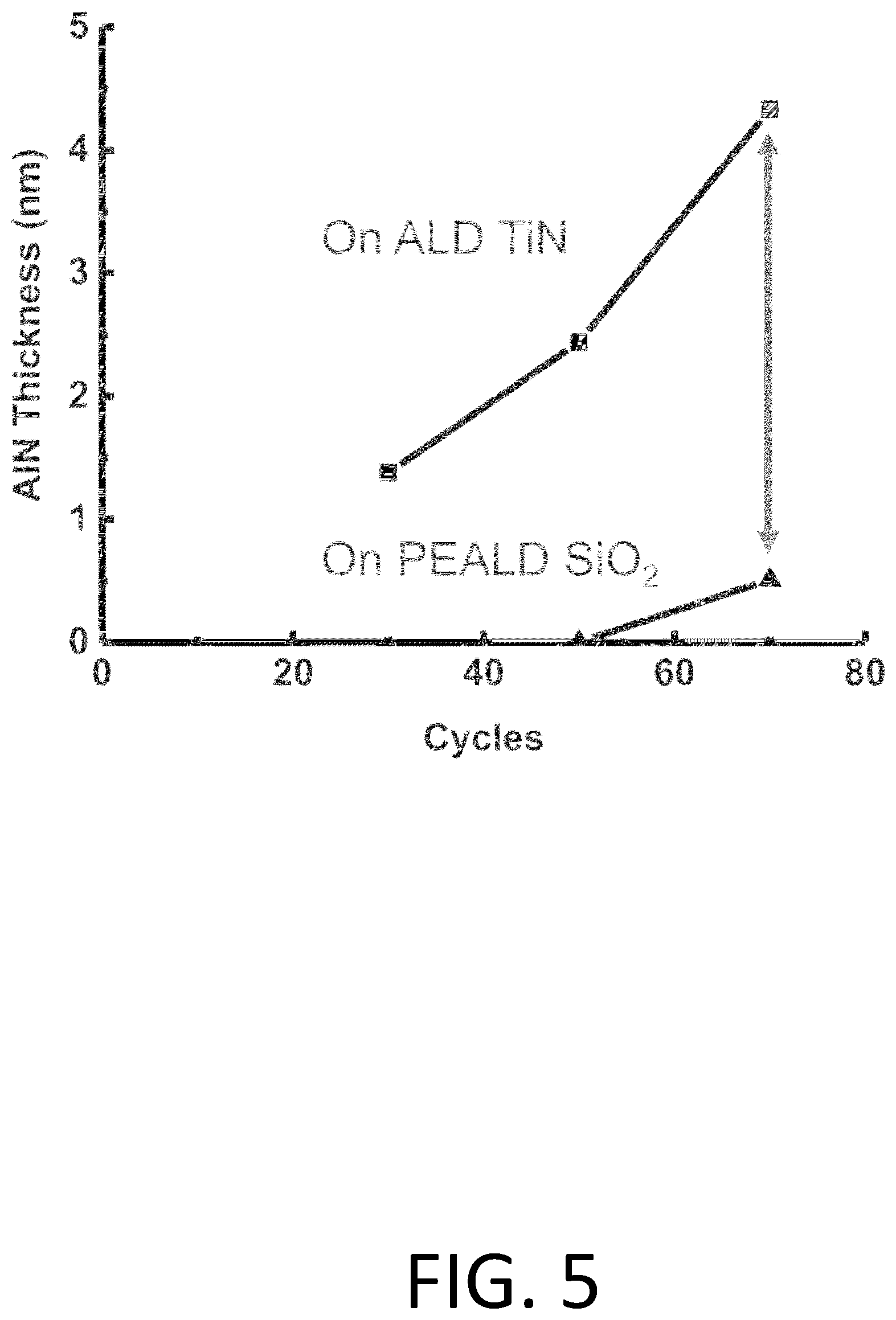
FIG. 5 is a graph of deposited material thickness versus number of deposition cycles for Al and N containing material selectively deposited on a first TiN surface relative to a second SiO.sub.2 surface;
FIG. 6 is a graph of deposited material thickness versus number of deposition cycles for Al and N containing material selectively deposited on a first TiN surface relative to a SiO.sub.2 and native oxide second surfaces;
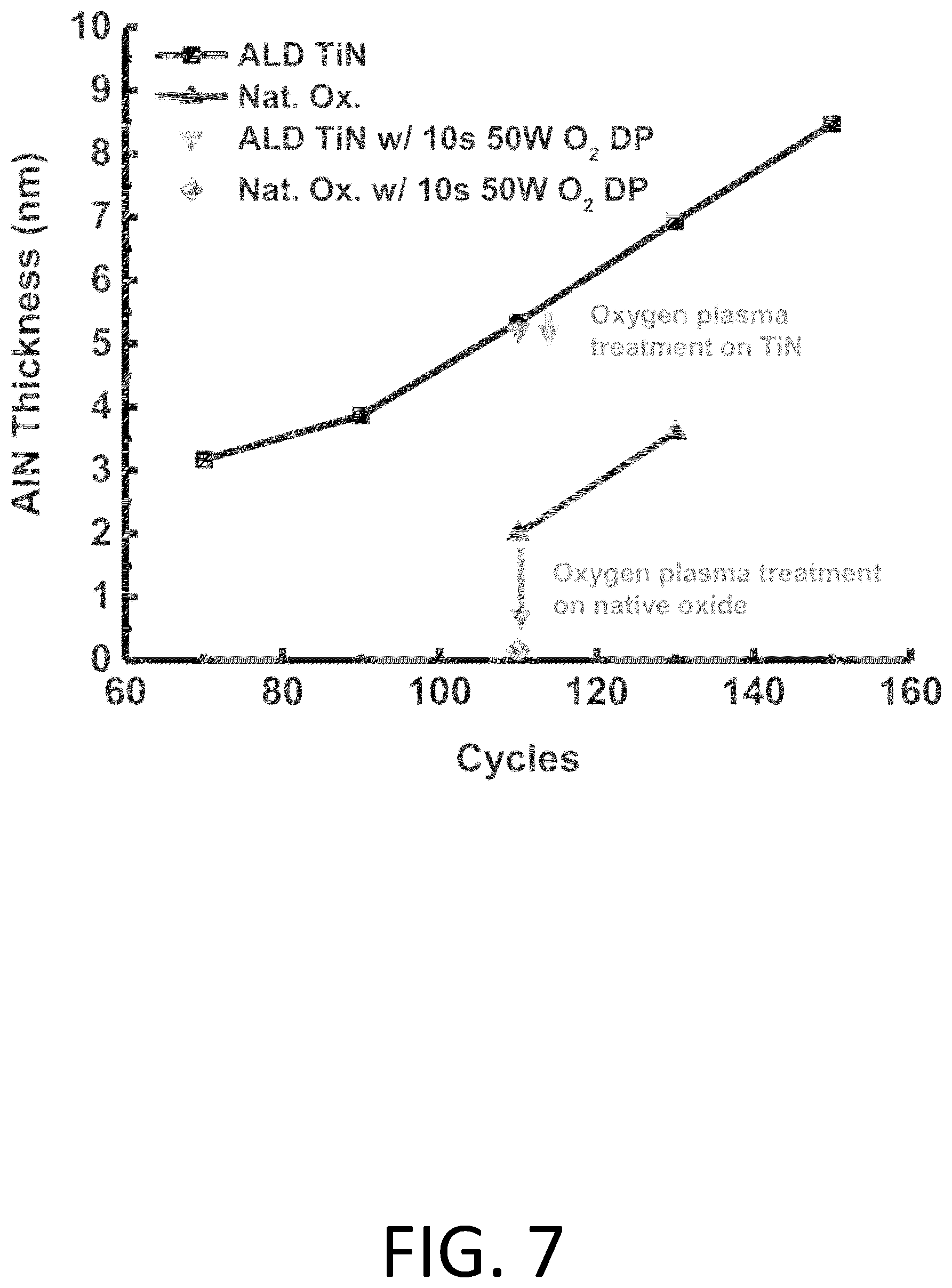
FIG. 7 is a graph of deposited material thickness versus number of deposition cycles for Al and N containing material selectively deposited on a first TiN surface relative to a second native oxide surface;
FIG. 8 is a graph of deposited material thickness versus number of deposition cycles for Al and N containing material selectively deposited on a first TiN or W surface relative to a second SiO.sub.2 surface.
DETAILED DESCRIPTION OF THE PREFERRED EMBODIMENT
In some situations it is desirable to selectively deposit a material comprising aluminum (Al) and nitrogen (N), such as aluminum nitride (AlN) on one surface of a substrate relative to a second, different surface of the same substrate. For example, selective deposition of an Al and N containing material may be used to form capping layers, barrier layers, or etch stop layers, such as a contact etch stop layer. For example, an Al and N containing material may be deposited selectively on a first surface of a substrate preferentially over a second, different surface, such as a dielectric surface of the same substrate.
In some embodiments a substrate comprising a first surface and a second, different surface is provided and a Al and N containing material is selectively deposited on the first surface relative to the second surface using an ALD type process comprising a plurality of deposition cycles, each cycle comprising alternately and sequentially contacting a substrate with a vapor phase first precursor and a vapor phase second precursor. In some embodiments the selectively deposited Al and N containing material is AlN.
In some embodiments an aluminum and nitrogen containing material, such as AlN, is selectively deposited on a metal surface of a substrate comprising both a conductive surface and a dielectric surface. In some embodiments, AlN is selectively deposited on a first conductive surface of a substrate, such as a Cu, W, or TiN surface relative to a second dielectric surface, such as a SiO.sub.2 or low-k surface of the same substrate. In some embodiments AlN is selectively deposited on a first surface that is not a conductive surface, such as a SiN surface, relative to a second dielectric surface, such as a SiO.sub.2 or low-k surface of the same substrate. In some embodiments AlN is selectively deposited on a Cu surface, relative to a second, different surface. In some embodiments AlN is selectively deposited on a W surface, relative to a second, different surface. In some embodiments AlN is selectively deposited on a TiN surface, relative to a second, different surface. In some embodiments AlN is selectively deposited on a SiN surface, relative to a second, different surface.
ALD Type Processes
ALD type processes are based on controlled, self-limiting surface reactions of precursor chemicals. Gas phase reactions are avoided by alternately and sequentially contacting the substrate with the precursors. Vapor phase reactants are separated from each other on the substrate surface, for example, by removing excess reactants and/or reactant byproducts from the reaction chamber between reactant pulses. In some embodiments one or more substrate surfaces are alternately and sequentially contacted with two or more vapor phase precursors, or reactants. Contacting a substrate surface with a vapor-phase reactant means that the reactant vapor is in contact with the substrate surface for a limited period of time. In other words, it can be understood that the substrate surface is exposed to each vapor phase reactant for a limited period of time.
Briefly, a substrate comprising at least a first surface and second, different surface is heated to a suitable deposition temperature, generally at lowered pressure. Deposition temperatures are generally maintained below the thermal decomposition temperature of the reactants but at a high enough level to avoid condensation of reactants and to provide the activation energy for the desired surface reactions. Of course, the appropriate temperature window for any given ALD reaction will depend upon the surface termination and reactant species involved. Here, the temperature varies depending on the precursors being used and is preferably at or below about 500.degree. C., preferably between about 250.degree. C. and about 500.degree. C., more preferably between about 275.degree. C. and about 450.degree. C., more preferably between about 300.degree. C. and about 425.degree. C., and most preferably between about 325.degree. C. and about 400.degree. C.
The surface of the substrate is contacted with a vapor phase first reactant. In some embodiments a pulse of vapor phase first reactant is provided to a reaction space containing the substrate. In some embodiments the substrate is moved to a reaction space containing vapor phase first reactant. Conditions are preferably selected such that no more than about one monolayer of the first reactant is adsorbed on the substrate surface in a self-limiting manner. The appropriate contacting times can be readily determined by the skilled artisan based on the particular circumstances. Excess first reactant and reaction byproducts, if any, are removed from the substrate surface, such as by purging with an inert gas or by removing the substrate from the presence of the first reactant.
Purging means that vapor phase precursors and/or vapor phase byproducts are removed from the substrate surface such as by evacuating a chamber with a vacuum pump and/or by replacing the gas inside a reactor with an inert gas such as argon or nitrogen. Typical purging times are from about 0.05 to 20 seconds, more preferably between about 1 and 10, and still more preferably between about 1 and 2 seconds. However, other purge times can be utilized if necessary, such as where highly conformal step coverage over extremely high aspect ratio structures or other structures with complex surface morphology is needed.
The surface of the substrate is contacted with a vapor phase second gaseous reactant. In some embodiments a pulse of a second gaseous reactant is provided to a reaction space containing the substrate. In some embodiments the substrate is moved to a reaction space containing the vapor phase second reactant. Excess second reactant and gaseous byproducts of the surface reaction, if any, are removed from the substrate surface. The steps of contacting and removing are repeated until a thin film of the desired thickness has been selectively formed on the first surface of substrate, with each cycle leaving no more than about a molecular monolayer. Additional phases comprising alternately and sequentially contacting the surface of a substrate with other reactants can be included to form more complicated materials, such as ternary materials.
As mentioned above, each phase of each cycle is preferably self-limiting. An excess of reactant precursors is supplied in each phase to saturate the susceptible structure surfaces. Surface saturation ensures reactant occupation of all available reactive sites (subject, for example, to physical size or "steric hindrance" restraints) and thus ensures excellent step coverage. Typically, less than one molecular layer of material is deposited with each cycle, however, in some embodiments more than one molecular layer is deposited during the cycle.
Removing excess reactants can include evacuating some of the contents of a reaction space and/or purging a reaction space with helium, nitrogen or another inert gas. In some embodiments purging can comprise turning off the flow of the reactive gas while continuing to flow an inert carrier gas to the reaction space.
The substrate can comprise various types of materials. When manufacturing integrated circuits, the substrate typically comprises a number of thin films with varying chemical and physical properties. For example and without limitation, the substrate may comprise a dielectric layer and a metal layer. In some embodiments the substrate can comprise metal carbide. In some embodiments the substrate can comprise a conductive oxide.
Preferably the substrate has a first surface comprising a conductive surface, such as metal or metallic surface. In some embodiments the first surface comprises a metal nitride. In some embodiments the first surface comprises one or more transition metals. The transition metal can be selected from the group: Ti, V, Cr, Mn, Nb, Mo, Ru, Rh, Pd, Ag, Au, Hf, Ta, W, Re, Os, Ir and Pt. In other embodiments the transition metal is selected from the group: Fe, Co, Ni. In some embodiments the first surface preferably comprises copper. In some embodiments the first surface comprises a noble metal. The noble metal can be selected from the group: Au, Pt, Ir, Pd, Os, Ag, Re, Rh, and Ru. In some preferred embodiments the first surface comprises at least one of Cu, W, TiN or SiN.
In some embodiments the first surface may comprise more than one material, for example TiN and SiN.
In some embodiments the first surface comprises a metal silicide, such as transition metal silicide. In some embodiments the first surface comprises a metallic film comprising a transition metal, such as a transition metal carbide or carbon-containing transition metal material. In some embodiments the first surface may comprise Al. In some embodiments the first surface comprises an alloy of metals or metallic materials.
The second surface is preferably a dielectric surface, such as SiO.sub.2, GeO.sub.2, or a low-k surface. In some embodiments, the dielectric comprises SiO.sub.2. In some embodiments the dielectric is a porous material. In some embodiments the porous dielectric contains pores which are connected to each other, while in other embodiments the pores are not connected to each other. In some embodiments the dielectric comprises a low-k material, defined as an insulator with a dielectric value below about 4.0. In some embodiments the dielectric value of the low-k material is below about 3.5, below about 3.0, below about 2.5 and below about 2.3. In some embodiments the second surface comprises Si--O bonds. In some embodiments the second surface is deactivated, for example by a plasma treatment. In some embodiments the second surface is a non-conducting surface. In some embodiments the second surface has a resistivity greater than about 1 ohmm. In some embodiments the second surface comprises Si--O bonds and has a resistivity less than about 1 ohmm. The term dielectric is used herein for the sake of simplicity in distinguishing from the other, first surface, namely the metal or metallic surface. Unless indicated otherwise with respect to particular embodiments, the term dielectric in the context of this application can be understood to indicate all surfaces which have a very high resistivity.
The precursors employed in the ALD type processes may be solid, liquid or gaseous materials under standard conditions (room temperature and atmospheric pressure), provided that the precursors are in vapor phase before they are contacted with the substrate surface. Contacting a substrate surface with a vaporized precursor means that the precursor vapor is in contact with the substrate surface for a limited period of time. Typically, the contacting time is from about 0.05 to 10 seconds. However, depending on the substrate type and its surface area, the contacting time may be even higher than 10 seconds. Contacting times can be on the order of minutes in some cases. The optimum contacting time can be determined by the skilled artisan based on the particular circumstances.
The mass flow rate of the precursors can also be determined by the skilled artisan. In some embodiments the flow rate of metal precursors is preferably between about 1 and 1000 sccm without limitation, more preferably between about 100 and 500 sccm.
The pressure in a reaction chamber is typically from about 0.01 to about 20 mbar, more preferably from about 1 to about 10 mbar. However, in some cases the pressure will be higher or lower than this range, as can be determined by the skilled artisan given the particular circumstances.
Before starting the deposition of the film, the substrate is typically heated to a suitable growth temperature. The growth temperature varies depending on the type of thin film formed, physical properties of the precursors, etc. The growth temperatures are discussed in greater detail below in reference to each type of thin film formed. The growth temperature can be less than the crystallization temperature for the deposited materials such that an amorphous thin film is formed or it can be above the crystallization temperature such that a crystalline thin film is formed. The preferred deposition temperature may vary depending on a number of factors such as, and without limitation, the reactant precursors, the pressure, flow rate, the arrangement of the reactor, crystallization temperature of the deposited thin film, and the composition of the substrate including the nature of the material to be deposited on. The specific growth temperature may be selected by the skilled artisan.
Reactors capable of being used to grow thin films can be used for the deposition. Such reactors include ALD reactors, as well as CVD reactors equipped with appropriate equipment and means for providing the precursors. According to some embodiments, a showerhead reactor may be used.
Examples of suitable reactors that may be used include commercially available equipment such as the F-120.RTM. reactor, F-450.RTM. reactor, Pulsar.RTM. reactors--such as the Pulsar.RTM. 2000 and the Pulsar.RTM. 3000--EmerALD.RTM. reactor and Advance.RTM. 400 Series reactors, available from ASM America, Inc. of Phoenix, Ariz. and ASM Europe B.V., Almere, Netherlands. Other commercially available reactors include those from ASM Japan K.K (Tokyo, Japan) under the tradename Eagle.RTM. XP and XP8.
In some embodiments a batch reactor may be used. Suitable batch reactors include, but are not limited to, reactors commercially available from and ASM Europe B.V (Almere, Netherlands) under the trade names ALDA400.TM. and A412.TM.. In some embodiments a vertical batch reactor is utilized in which the boat rotates during processing, such as the A412.TM.. Thus, in some embodiments the wafers rotate during processing. In some embodiments in which a batch reactor is used, wafer-to-wafer uniformity is less than 3% (1sigma), less than 2%, less than 1% or even less than 0.5%.
The growth processes can optionally be carried out in a reactor or reaction space connected to a cluster tool. In a cluster tool, because each reaction space is dedicated to one type of process, the temperature of the reaction space in each module can be kept constant, which improves the throughput compared to a reactor in which the substrate is heated up to the process temperature before each run.
A stand-alone reactor can be equipped with a load-lock. In that case, it is not necessary to cool down the reaction space between each run.
Preferably, for forming an Al and N containing material, each ALD cycle comprises at least two distinct phase. Contacting the substrate with a first precursor and thereafter removing excess first precursor and reaction byproducts from the substrate surface may be considered a phase and may be referred to as a first phase, first precursor phase, Al phase, Al precursor phase, first Al phase, and/or first Al precursor phase. For a deposition cycle, in a first phase, the substrate is contacted with a first precursor comprising Al, which forms no more than about one monolayer on the substrate surface. In a second phase, the substrate is contacted with a second precursor comprising nitrogen and may convert adsorbed first precursor to an Al and N containing material. Contacting the substrate with a second precursor and thereafter removing excess second precursor and reaction byproducts from the substrate surface may be considered a phase and may be referred to as a second phase, second precursor phase, N phase, N precursor phase, first N phase, and/or first N precursor phase. One or more of the precursors may be provided with the aid of a carrier gas, such as N.sub.2, Ar, or He. Additional phases may be added and phases may be removed as desired to adjust the composition of the final film.
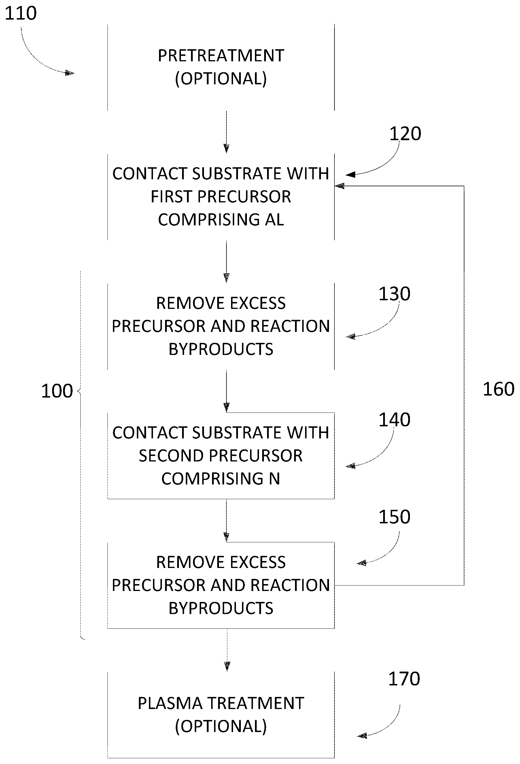
Referring to FIG. 1 and according to preferred embodiments an Al and N containing material is selectively deposited on a first surface of a substrate comprising a first surface and a second, different surface by an ALD type deposition process 100 comprising at least one cycle comprising:
contacting the substrate with a first vapor phase precursor comprising Al at step 120;
removing excess first precursor and reaction by products, if any, from the substrate at step 130;
contacting the substrate with a second vapor phase precursor comprising nitrogen at step 140;
removing from the substrate, at step 150, excess second precursor and any gaseous by-products, and;
optionally repeating at step 160 the contacting and removing steps until an Al and N containing material of the desired thickness has been formed.
In some embodiments one or more surfaces of the substrate may be subjected to a pretreatment process prior to beginning the deposition process 100. In some embodiments a pretreatment process may enhance the selectivity of the selective deposition process 100. In some embodiments a pretreatment process may enhance deposition of an Al and N containing material on one surface relative to one or more different surfaces prior to beginning the deposition process 100. In some embodiments a pretreatment process may inhibit deposition of an Al and N containing material on one surface relative to one or more different surface prior to beginning the deposition process 100. In FIG. 1 this is indicated by step 110 in which the substrate can be exposed to a pretreatment reactant, for example a plasma, prior to deposition of an Al and N containing material.
In some embodiments a pretreatment process may comprise exposing the substrate to a pretreatment reactant. In some embodiments a pretreatment reactant may comprise oxygen. In some embodiments the pretreatment reactant comprises oxygen radicals, atomic oxygen, oxygen plasma, or combinations thereof. In some embodiments a pretreatment reactant may comprise nitrogen. In some embodiments the pretreatment reactant comprises nitrogen radicals, atomic nitrogen, nitrogen plasma, or combinations thereof. In some embodiments a pretreatment reactant may comprise hydrogen. In some embodiments the pretreatment reactant comprises hydrogen radicals, atomic hydrogen, hydrogen plasma, or combinations thereof.
In some embodiments utilizing a pretreatment process wherein the substrate is exposed to a pretreatment reactant comprising oxygen plasma, O.sub.2 may be provided, for example, from about 1 to about 2000 sccm, more preferably from about 5 to about 1000 sccm, and most preferably from about 50 to about 500 sccm. In some embodiments O.sub.2 may be provide at about 300 sccm. In some embodiments utilizing a pretreatment process wherein the substrate is exposed to a pretreatment reactant comprising nitrogen plasma, N.sub.2 may be provided, for example, at about from about 1 to about 5000 sccm, more preferably from about 5 to about 2000 sccm, and most preferably from about 50 to about 500 sccm. In some embodiments N.sub.2 may be provided at about 300 sccm. In some embodiments a pretreatment process wherein the substrate is exposed to a pretreatment reactant comprising hydrogen plasma, H.sub.2 may be provided, for example, from about 1 to about 2000 sccm, more preferably from about 5 to about 1000 sccm, and most preferably from about 10 to about 100 sccm. In some embodiments H.sub.2 may be provided at about 50 sccm. Similar conditions can be used for other types of plasma.
In some embodiments a pretreatment process may comprise exposing the substrate to a pretreatment reactant at a pretreatment temperature. In some embodiments the pretreatment temperature may be great than about 20.degree. C. In some embodiments a pretreatment temperature may be between about 20.degree. C. and about 500.degree. C., more preferably between about 50.degree. C. and about 450.degree. C., more preferably between about 150.degree. C. and about 400.degree. C. In some embodiments the pretreatment temperature may be about the same as the deposition temperature. In some embodiments the pretreatment temperature may be different than the deposition temperature. In some embodiments plasma may be generated at a power of less than about 2500 Watts, for example about 1 to about 1000 Watts, about 1 to about 500 W, or about 1 to about 200 W or less. In some embodiments plasma may be generated at a power of 50 W. In some embodiments plasma may be generated at a power of 100 W.
In some embodiments the plasma is provided for less than about 200 seconds, for example about 180 seconds or less, about 60 seconds or less, about 30 seconds or less, about 10 seconds or less, or about 3 seconds or less.
In some embodiments, plasma is formed in a reactor. In some embodiments, the plasma may be formed in situ on top of the substrate or in close proximity to the substrate. In other embodiments, the plasma is formed upstream of the reaction chamber in a remote plasma generator and plasma products are directed to the reaction chamber to contact the substrate. As will be appreciated by the skilled artisan, in the case of remote plasma, the pathway to the substrate can be optimized to maximize electrically neutral species and minimize ion survival before reaching the substrate.
In some embodiments the treated substrate is not exposed to the ambient environment after a pretreatment process and before beginning a selective deposition process. In some embodiments the treated substrate is not exposed to air after a pretreatment process and before beginning a selective deposition process.
In some embodiments a pretreatment process may be used to enhance the selectivity of the subsequent selective deposition process. In some embodiments a pretreatment process may enhance selective deposition of an Al and N containing material on a first surface relative to a second different surface. In some embodiments a pretreatment process may enhance the selectivity of a subsequent selective deposition process by a factor of more than about 2, more than about 5, or more than about 10.
In some embodiments a pretreatment process may be performed in the same reaction chamber or reactor as the subsequent deposition process 100. In some embodiments a pretreatment process may be performed in a different reaction chamber or reactor than the subsequent deposition process 100.
Referring again to FIG. 1, the substrate is contacted with a first precursor comprising Al at step 120. In some embodiments the first precursor is conducted into a reaction chamber in the form of vapor phase pulse and contacted with the surface of the substrate. Conditions are preferably selected such that no more than about one monolayer of the precursor is adsorbed on the substrate surface in a self-limiting manner. However, in some embodiments conditions may be selected such that more than one monolayer of the precursor may be formed.
The first precursor pulse is preferably supplied in gaseous form. The first precursor gas is considered "volatile" for purposes of the present description if the species exhibits sufficient vapor pressure under the process conditions to transport the species to the workpiece in sufficient concentration to saturate exposed surfaces.
In some embodiments the first precursor contacts the substrate for about 0.01 seconds to about 60 seconds, for about 0.02 seconds to about 30 seconds, for about 0.025 seconds to about 20 seconds, for about 0.05 seconds to about 5.0 seconds, about 0.05 seconds to about 2.0 seconds or about 0.1 seconds to about 1.0 second.
The first precursor employed in the ALD type processes may be solid, liquid, or gaseous material under standard conditions (room temperature and atmospheric pressure), provided that the first precursor is in vapor phase before it is conducted into the reaction chamber and contacted with the substrate surface.
At step 130 excess first precursor and reaction byproducts, if any, are removed from the substrate surface, for example by purging with a pulse of inert gas such as nitrogen or argon. Purging the reaction chamber means that vapor phase precursors and/or vapor phase byproducts are removed from the reaction chamber such as by evacuating the chamber with a vacuum pump and/or by replacing the gas inside the reactor with an inert gas such as argon or nitrogen. Typical purging times are from about 0.05 to 20 seconds, more preferably between about 1 and 10 seconds, and still more preferably between about 1 and 2 seconds. However, other purge times can be utilized if necessary, such as when depositing layers over extremely high aspect ratio structures or other structures with complex surface morphology is needed. The appropriate purging times can be readily determined by the skilled artisan based on the particular circumstances.
In other embodiments however, removing excess first precursor and reaction byproducts, if any, may comprise moving the substrate so that the first precursor no longer contacts the substrate. In some embodiments no precursor may be removed from the various parts of a chamber. In some embodiments the substrate is moved from a part of the chamber containing a first precursor to another part of the chamber containing a second precursor or no precursor at all. In some embodiments the substrate is moved from a first reaction chamber to a second, different reaction chamber.
At step 140 the substrate is contacted with a second vapor phase precursor comprising N. In some embodiments the second precursor is pulsed into the chamber where it reacts with the first precursor bound to the first surface of the substrate. The reaction typically forms up to about a monolayer of an Al and N containing material on the substrate. In some embodiments, however, more than one molecular layer of an Al and N containing material is formed on the substrate.
In some embodiments, the second precursor may include nitrogen plasma or nitrogen radicals. In such embodiments, nitrogen may be energized within the reaction chamber or upstream of the reaction chamber. Where a plasma is desired, the flow of un-energized second precursor may comprise a type of purge gas, such that after the substrate has been exposed to a nitrogen plasma for a desired period of time, the plasma generator may be turned off and the flow of nitrogen precursor itself is used to clear the reaction chamber of excess nitrogen plasma and unreacted byproducts.
While one skilled in the art will recognize that any number of suitable second precursors may be used, appropriate second precursors include nitrogen containing compounds that favorably react with the ligands of a previously or subsequently deposited first precursor. Accordingly, selection of an appropriate second precursor may depend on the specific first precursor used and the nature of the ligands in the first precursor
In some embodiments the second precursor contacts the substrate for about 0.01 seconds to about 60 seconds, for about 0.02 seconds to about 30 seconds, for about 0.025 seconds to about 20 seconds, for about 0.05 seconds to about 5.0 seconds, about 0.05 seconds to about 2.0 seconds or about 0.1 seconds to about 1.0 second. However, depending on the reactor type, substrate type and its surface area, the second precursor contacting time may be even higher than 10 seconds. In some embodiments, contacting times can be on the order of minutes. The optimum contacting time can be readily determined by the skilled artisan based on the particular circumstances.
The concentration of the second precursor in the reaction chamber may be from about 0.01% by volume to about 99.0% by volume. And the second precursor may flow through the reaction chamber at a rate of between about 1 standard cm.sup.3/min and about 4000 standard cm.sup.3/min.
At step 150, excess second precursor and gaseous by-products of the surface reaction, if any, are removed from the substrate, as described above for step 130. In some embodiments excess precursor and reaction byproducts are preferably removed with the aid of an inert gas.
The steps of contacting and removing may be optionally repeated at step 160 until an Al and N containing material of a desired thickness has been formed on the first surface of the substrate, with each cycle leaving no more than about a molecular monolayer. In some cases, it might be desirable to achieve at least partial decomposition of at least one the various precursors. Thus, in some embodiments conditions may be selected such that more than one molecular layer of an Al and N containing material is formed on the substrate in each deposition cycle.
The Al and N containing material ALD processes of the present disclosure may comprise one or more cycles. Some embodiments involve the repetition of at least about 5 cycles, at least about 10 cycles, or at least about 50 cycles. In some embodiments, no more than 100 cycles are performed to form a thin film of a desirable thickness.
In some embodiments the substrate surface and/or Al and N containing material may optionally be subjected to a plasma treatment process. In FIG. 1 this is indicated by step 170. In some embodiments the plasma treatment process may be performed after more than one deposition cycle has been performed. In some embodiments a plasma treatment process may be performed before the deposited Al and N containing material film is continuous or closed. In some embodiments a plasma treatment process may be performed after about every 10 deposition cycles, after about every 20 deposition cycles, or after about every 50 deposition cycles. In some embodiments at least 2 consecutive deposition cycles are performed without a plasma treatment process. In some embodiments at least 5 or 10 deposition cycles are performed without a plasma treatment process. In some embodiments a plasma treatment process may be performed before any deposition been carried out; that is, before any deposition cycle is performed.
In some embodiments a plasma treatment process may be performed in the same reaction chamber or reactor as the deposition process 100. In some embodiments a plasma treatment process may be performed in a different reaction chamber or reactor than the deposition process 100.
In some embodiments, plasma is formed in a reactor. In some embodiments, the plasma may be formed in situ on top of the substrate or in close proximity to the substrate. In other embodiments, the plasma is formed upstream of the reaction chamber in a remote plasma generator and plasma products are directed to the reaction chamber to contact the substrate. As will be appreciated by the skilled artisan, in the case of remote plasma, the pathway to the substrate can be optimized to maximize electrically neutral species and minimize ion survival before reaching the substrate.
In some embodiments, the Al and N containing material can be deposited using a plurality of deposition cycles, and the plasma treatment can be applied at one or more times, including, for example, before deposition, after every deposition cycle, at predetermined intervals during deposition, or after an Al and N containing material of desired thickness is deposited.
In some embodiments a plasma treatment process comprises exposing the substrate to direct plasma. In some embodiments a plasma treatment process comprises exposing the substrate to remote plasma. In some embodiments a plasma treatment process comprises exposing the substrate to excited species or atomic species created in plasma discharge but does not comprise a substantial amount, if any, of ions. In some embodiments the plasma may comprise oxygen. In some embodiments the plasma may comprise nitrogen. Although referred to as a plasma treatment process, in some embodiments a reactive oxygen species that does not comprise plasma may be used, for example ozone. In some embodiments the plasma may comprise hydrogen.
In some embodiments utilizing a pretreatment process or plasma treatment process the substrate is exposed to a reactant comprising oxygen plasma. O.sub.2 may be provided as a source gas, for example, from about 1 to about 2000 sccm, more preferably from about 5 to about 1000 sccm, and most preferably from about 50 to about 500 sccm. In some embodiments O.sub.2 may be provide at about 300 sccm.
In some embodiments utilizing a pretreatment process or plasma treatment process the substrate is exposed to a reactant comprising nitrogen plasma. N.sub.2 may be provided as a source gas, for example, at about from about 1 to about 5000 sccm, more preferably from about 5 to about 2000 sccm, and most preferably from about 50 to about 500 sccm. In some embodiments N.sub.2 may be provided at about 300 sccm.
In some embodiments utilizing a pretreatment process or plasma treatment process the substrate is exposed to a reactant comprising hydrogen plasma. In some embodiments, H.sub.2 may be provided as a source gas, for example, from about 1 to about 2000 sccm, more preferably from about 5 to about 1000 sccm, and most preferably from about 10 to about 100 sccm. In some embodiments H.sub.2 may be provided at about 50 sccm. Similar conditions can be used for other types of plasma.
In some embodiments a plasma treatment process may comprise exposing the substrate to a reactant at a treatment temperature. In some embodiments the treatment temperature may be great than about 20.degree. C. In some embodiments a treatment temperature may be between about 20.degree. C. and about 500.degree. C., more preferably between about 50.degree. C. and about 450.degree. C., more preferably between about 150.degree. C. and about 400.degree. C. In some embodiments the treatment temperature may be about the same as the deposition temperature and/or the pretreatment temperature. In some embodiments the treatment temperature may be different than the deposition temperature and/or pretreatment temperature.
In some embodiments plasma may be generated at a power of less than about 2500 Watts, for example about 1 to about 1000 Watts, about 1 to about 500 W, or about 1 to about 200 W or less. In some embodiments plasma may be generated at a power of 50 W. In some embodiments plasma may be generated at a power of 100 W.
In some embodiments the plasma is provided for less than about 200 seconds, for example about 180 seconds or less, about 60 seconds or less, about 30 seconds or less, about 10 seconds or less, or about 3 seconds or less.
In some embodiments a plasma treatment process 170 may be substantially identical to a pretreatment process 110.
Although the illustrated Al and N containing material deposition cycle begins with contacting the surface of the substrate with the first vapor phase precursor comprising Al, in other embodiments the deposition cycle begins with contacting the surface of the substrate with the second vapor phase precursor comprising nitrogen. It will be understood by the skilled artisan that contacting the substrate surface with the first vapor phase precursor comprising Al and second vapor phase precursor comprising nitrogen are interchangeable in the deposition cycle.
In some embodiments the substrate is moved such that different reactants alternately and sequentially contact the surface of the substrate in a desired sequence for a desired time. In some embodiments the removing steps, 130 and 150 are not performed. In some embodiments no reactant may be removed from the various parts of a chamber. In some embodiments the substrate is moved from a part of the chamber containing a first precursor to another part of the chamber containing the second reactant. In some embodiments the substrate is moved from a first reaction chamber to a second, different reaction chamber.
The skilled artisan can determine the optimal reactant evaporation temperatures based on the properties of the selected precursors. The skilled artisan can determine the optimal reactant contact times through routine experimentation based on the properties of the selected precursors and the desired properties of the deposited Al and N containing material.
The growth rate of the Al and N containing materials will vary depending on the reaction conditions. As described below, in initial experiments, the growth rate varied between about 0.01 and about 2.0 .ANG./cycle. In some embodiments the growth rate may be from about 0.01 .ANG./cycle to about 3.0 .ANG./cycle, preferably from about 0.1 .ANG./cycle to about 2.5 .ANG./cycle, more preferably 0.3 .ANG./cycle to about 2.0 .ANG./cycle.
In some embodiments the deposited Al and N containing material comprises a thin film. In some embodiments the deposited Al and N containing material comprises AlN, and in some embodiments the deposited Al and N containing material is AlN. In some embodiments Al and N containing materials are formed that consist essentially of Al and N. In some embodiments, additional reactants may be used to incorporate into or contribute other materials to the film, for example oxygen to form aluminum oxynitrides. In some embodiments where additional non-metal elements in addition to nitrogen are desired, an ALD process for forming the Al and N containing material may comprise phases in addition to the initial Al and N phases. For example, they may include an oxidation phase where metal aluminum oxynitrides are desired. In an oxidation phase, oxygen or an oxygen-containing precursor is provided in the reaction chamber and allowed to contact the substrate surface. The oxygen phase may be part of one or more deposition cycles. In some embodiments a second metal phase may be provided in one or more deposition cycles. The oxidation phase, or other desirable phase, may follow the Al phase or the N phase, but in either situation, it is desirable in some embodiments, to remove excess oxygen (or other reactant) and any reaction by-products from the reaction space before proceeding to the next phase. In some embodiments an additional phase, such as an oxygen, or additional metal phase may be provided after the final deposition cycle, or intermittently in the deposition process.
In some embodiments deposition of an Al and N containing material on a first surface of a substrate relative to a second surface of the substrate is at least about 90% selective, at least about 95% selective, at least about 96%, 97%, 98% or 99% or greater selective. In some embodiments deposition of an Al and N containing material only occurs on the first surface and does not occur on the second surface. In some embodiments deposition on the first surface of the substrate relative to the second surface of the substrate is at least about 80% selective, which may be selective enough for some particular applications. In some embodiments the deposition on the first surface of the substrate relative to the second surface of the substrate is at least about 50% selective, which may be selective enough for some particular application.
In some embodiments the ratio of Al and N containing material deposited on a first surface of a substrate relative to a second surface of the substrate may be greater than or equal to about 10:1, greater than or equal to about 20:1, or greater than or equal to about 40:1. In some embodiments the ratio of Al and N containing material deposited on a first surface of a substrate relative to a second surface of the substrate may be greater than or equal to about 10:1, greater than or equal to about 20:1, or greater than or equal to about 40:1 when the thickness of Al and N containing material deposited on the first surface is more than about 5 nm. In some embodiments the ratio of Al and N containing material deposited on a first surface of a substrate relative to a second surface of the substrate may be greater than or equal to about 10:1, greater than or equal to about 20:1, or greater than or equal to about 40:1 when the thickness of Al and N containing material deposited on the first surface is more than about 2.5 nm. In some embodiments the ratio of Al and N containing material deposited on a first surface of a substrate relative to a second surface of the substrate may be greater than or equal to about 10:1, greater than or equal to about 20:1, or greater than or equal to about 40:1 when the thickness of Al and N containing material deposited on the first surface is more than about 1 nm.
In some embodiments the ratio of Al and N containing material deposited on a first surface of a substrate relative to a second surface of the substrate may be greater than or equal to about 10:1, greater than or equal to about 20:1, or greater than or equal to about 40:1 when the Al and N containing material deposition process comprises between about 0 and about 25 deposition cycles, between about 0 and about 50 deposition cycles, between about 0 and about 100 deposition cycles, or between about 0 and about 150 deposition cycles. In some embodiments less than about 0.1 nm of Al and N containing material is deposited on the second surface of the substrate when an Al and N containing material deposition process comprises between about 0 and about 25 deposition cycles, between about 0 and about 50 deposition cycles, between about 0 and about 100 deposition cycles, or between about 0 and about 150 deposition cycles.
In some embodiments an Al and N containing material has etch selectivity relative to SiO.sub.2, that is an Al and N containing material has an etch rate less than an etch rate of SiO.sub.2, for example in dilute HF. In some embodiments an Al and N containing material has a wet etch rate (WER) of less than 1/5 the thermal oxide removal rate of about 2-3 nm per minute with diluted HF (0.5%). In some embodiments the wet etch rate of the Al and N containing material relative to the wet etch rate of thermally oxidized silicon (SiO.sub.2, TOX) is less than about 0.2 in 0.5% dHF. In some embodiments the wet etch rate of the Al and N containing material relative to the wet etch rate of TOX is less than about 0.1 in 0.5% dHF. In some embodiments the wet etch rate of the Al and N containing material relative to the wet etch rate of TOX is less than about 0.05 in 0.5% dHF.
Referring now to FIG. 2, in some embodiments a substrate comprising a first surface and a second dielectric surface is provided and AlN is selectively deposited on the first surface of the substrate by a cyclical deposition process 200 comprising at least one cycle comprising:
contacting the substrate with vapor phase trimethylaluminum (TMA) at step 220;
removing excess TMA and reaction by products, if any, from the surface at step 230;
contacting the substrate with vapor phase NH.sub.3 at step 240;
removing from the surface excess NH.sub.3 and any by-products at step 250, and;
optionally repeating at step 260 the contacting and removing steps until an AlN thin film of the desired thickness has been formed.
Although the illustrated AlN deposition cycle begins with contacting the substrate with TMA, in other embodiments the deposition cycle begins with contacting the substrate with NH.sub.3. It will be understood by the skilled artisan that contacting the substrate surface with TMA and NH.sub.3 are interchangeable in the deposition cycle.
In some embodiments one or more surfaces of the substrate may be subjected to a pretreatment process prior to beginning the deposition process. In some embodiments a pretreatment process may enhance the selectivity of the selective deposition process 200. In some embodiments a pretreatment process may enhance deposition of AlN on one surface relative to one or more different surfaces prior to beginning the deposition process. In some embodiments a pretreatment process may inhibit the deposition of AlN on one surface relative to one or more different surface prior to beginning the deposition process. In FIG. 2 this is indicated by step 210 in which the substrate can be exposed to a pretreatment reactant, for example a plasma, prior to deposition of the Al and N containing material.
In some embodiments the substrate surface and/or AlN thin film may optionally be subjected to a plasma treatment process. In FIG. 2 this is indicated by step 270. In some embodiments this plasma treatment process may be substantially the same as the plasma treatment process 170 described above with respect to FIG. 1. In some embodiments the plasma treatment process 270 may be substantially identical to the pretreatment step 210. In some embodiments the plasma treatment process may be performed after more than one deposition cycle has been performed. In some embodiments a plasma treatment process may be performed before the deposited AlN film is continuous or closed. In some embodiments a plasma treatment process may be performed after more than about 10 deposition cycles, after more than about 20 deposition cycles, or after more than about 50 deposition cycles. In some embodiments a plasma treatment process may be performed in the same reaction chamber or reactor as the deposition process 200. In some embodiments a plasma treatment process may be performed in a different reaction chamber or reactor than the deposition process 200.
In some embodiments a substrate comprising a first surface and a second dielectric surface is provided and an Al and N containing material is selectively deposited on the first surface of the substrate by a cyclical deposition process comprising at least one cycle comprising alternately and sequentially contacting the substrate with a vapor phase first precursor and a vapor phase second precursor. In some embodiments the first precursor may comprise Al and the second precursor may comprise N. In some embodiments the first precursor may comprise tritertbutylaluminum and the second precursor may comprise NH.sub.3.
In some embodiments a substrate comprising a first surface and a second dielectric surface is provided and AlN is selectively deposited on the first surface of the substrate by a cyclical deposition process comprising at least one cycle comprising alternately and sequentially contacting the substrate with a vapor phase first precursor and a vapor phase second precursor. In some embodiments the first precursor may comprise Al and the second precursor may comprise N. In some embodiments the first precursor may comprise tritertbutylaluminum and the second precursor may comprise NH.sub.3.
In some embodiments a substrate is provided and AlN is deposited on at least part of the substrate by a cyclical deposition process comprising at least one cycle comprising alternately and sequentially contacting the substrate with a vapor phase first precursor and a vapor phase second precursor and the first precursor may comprise tritertbutylaluminum and the second precursor may comprise NH.sub.3.
In some embodiments, prior to deposition the substrate may be subjected to a pretreatment process. In some embodiments a pretreatment process may enhance the selectivity of the selective deposition process. In some embodiments a pretreatment process may enhance deposition of AlN on one surface relative to one or more different surfaces prior to beginning the deposition process. In some embodiments a pretreatment process may inhibit deposition of AlN on one surface relative to one or more different surface prior to beginning the deposition process. In some embodiments a pretreatment process may comprise exposing the substrate to a pretreatment reactant, for example plasma, prior to deposition of AlN.
In some embodiments the substrate surface and/or AlN thin film may optionally be subjected to a plasma treatment process. In some embodiments this plasma treatment process may be substantially the same as the plasma treatment processes 170 and 270 described above with respect to FIG. 1 and FIG. 2. In some embodiments the plasma treatment process may be substantially identical to the pretreatment process. In some embodiments the plasma treatment process may be performed after more than one deposition cycle has been performed. In some embodiments a plasma treatment process may be performed before the deposited AlN film is continuous or closed. In some embodiments a plasma treatment process may be performed after less than about 10 deposition cycles, after less than about 20 deposition cycles, or after less than about 50 deposition cycles. In some embodiments a plasma treatment process may be performed in the same reaction chamber or reactor as the deposition process. In some embodiments a plasma treatment process may be performed in a different reaction chamber or reactor than the deposition process.
First Precursors
A number of different first precursors can be used in the selective deposition process described herein. In some embodiments the first precursor is an organometallic compound comprising aluminum. In some embodiments the first precursor is an alkylaluminum compound. In some embodiments the first precursor does not comprise any other metals than aluminum.
In some embodiments the first precursor is a compound having the formula R.sub.3Al, where R is an alkyl group. Each R can be independently selected from the list of: methyl, ethyl, propyl, isopropyl, n-butyl, isobutyl, and tertbutyl groups. Preferably each R can be independently selected from: methyl, ethyl and tertbutyl groups. In some embodiments, each R can be independently selected from C.sub.1-C.sub.4 alkyl groups.
In some embodiments the first precursor comprises Me.sub.3Al, Et.sub.3Al, or .sup.tBu.sub.3Al. In some embodiments the first precursor is tritertbutylaluminum (TTBA) As mentioned above, in some embodiments the first precursor is trimethylaluminum (TMA).
In some embodiments the first precursor is not a halide. In some embodiments the first precursor may comprise a halogen in at least one ligand, but not in all ligands. In some embodiments the first precursor comprises one chlorine ligand and two alkyl ligands. In some embodiments the first precursor is AlCl.sub.3.
In some embodiments the first precursor may comprise hydrogen as at least one ligand, but not all ligands. In some embodiments the first precursor may comprise at least one hydrogen ligand and at least one alkyl ligand.
In some embodiments the first precursor does not comprise nitrogen. In some embodiments the first precursor does not comprise silicon. In some embodiments the first precursor does not comprise oxygen. In some embodiments the first precursor does not comprise nitrogen, silicon, or oxygen.
Second Precursors
In some embodiments the second precursor comprises a nitrogen-hydrogen bond. In some embodiments the second precursor is ammonia (NH.sub.3). In some embodiments, the second precursor is molecular nitrogen. In some embodiments the second precursor is a nitrogen containing plasma. In some embodiments the second precursor is a nitrogen containing plasma, such as nitrogen and hydrogen containing plasma In some embodiments, the second precursor comprises an activated or excited nitrogen species. In some embodiments the second precursor may be a provided in a nitrogen-containing gas pulse that can be a mixture of nitrogen reactant and inactive gas, such as argon.
Integration
The Al and N containing material of the present disclosure may be used in a variety of semiconductor applications. For example, Al and N containing material may be particularly useful as an etch stop layer, for example a contact etch stop layer, in a self-aligned contact formation process. Self-aligned source/drain contacts can be used to provide a misalignment margin for contact lithography. However, a standard self-aligned contact process requires additional processing steps such as a multiple metal recess step, a SiN fill step, and a SiN polish step using chemical-mechanical planarization.
In addition, the need for future scaling of the SiN sidewall spacer and etch stop layer in the standard self-aligned contact process due to increasing device miniaturization may create a risk of short-circuiting between the contact and the metal gate due to spacer or etch stop layer over-etching.
In some embodiments an Al and N containing material of the present disclosure may be used as a etch stop layer in a self-aligned contact process that does not include a metal recess. In some embodiments an Al an N containing material of the present disclosure is etch resistant. FIG. 3 illustrates a process flow for a self-aligned contact process including an Al and N containing material protective layer, capping layer, or etch stop layer, according to some embodiments. In some embodiments a process for forming of a self-aligned contact 300 proceeds as follows:
a semiconductor substrate comprising a first surface and a second, different surface overlying a source/drain region is provided at step 301;
an Al and N containing protective layer or etch stop layer, for example AlN, is selectively deposited on the first surface of the substrate relative to the second surface, at step 302;
the second surface is removed, for example using a wet etch process, at step 303; and
a contact is formed in place of the removed second surface over a source/drain region of the substrate at step 304.
According to some embodiments, at step 301, a substrate comprising a semiconductor is provided. The semiconductor substrate comprises a first surface and a second, different surface. In some embodiments the first surface comprises a conductive surface. In some embodiments the first surface comprises one or more metal nitrides. In some embodiments the first surface may comprise the surface of a conductive gate and/or the surface of a spacer. For example, in some embodiments the first surface may comprise a TiN gate and a SiN spacer. The second surface is preferably a dielectric surface. In some embodiments the dielectric comprises SiO.sub.2. In some embodiments the second surface is a dummy contact overlying a source/drain region. In some embodiments the SiO.sub.2 dummy contact directly overlies a source/drain region.
In some embodiments the semiconductor substrate is subjected to a standard process through gate polish. That is, a semiconductor substrate may be subjected to a standard replaced metal gate process flow to form a source, gate, and drain as is well known in the art. In some embodiments a semiconductor substrate may be subjected to a chemical-mechanical planarization process.
An Al and N containing protective layer or etch stop layer is selectively deposited on the first surface of the substrate relative to the second surface at step 302. In some embodiments the Al an N containing protective material is formed over a TiN gate and a SiN spacer. In some embodiments the Al and N containing protective material is formed directly over a TiN gate and a SiN spacer.
In some embodiments the Al and N containing protective layer is deposited by an ALD process as described herein. In some embodiments the substrate is alternately and sequentially contacted with a first precursor comprising Al and a second precursor comprising N. In some embodiments the Al and N containing protective layer comprises AlN. In some embodiments the Al and N containing protective layer comprises an AlN thin film.
In some embodiments deposition of the Al and N containing protective layer on the first surface of the substrate relative to the second surface of the substrate is at least about 90% selective, at least about 95% selective, at least about 96%, 97%, 98% or 99% or greater selective. In some embodiments deposition of the Al and N containing material only occurs on the first surface and does not occur on the second surface. In some embodiments deposition on the first surface of the substrate relative to the second surface of the substrate is at least about 80% selective, or at least about 50% selective.
In some embodiments, the Al and N containing protective layer or etch stop layer is deposited on the first surface of the substrate to achieve a particular thickness. Suitable thicknesses may be greater than or equal to about 0.1 nm and less than or equal to about 10 nm. In some embodiments, the thickness will be between about 0.1 nm and about 5 nm. In some embodiments, the thickness will be between about 1 nm and about 5 nm. In some embodiments, the thickness is between about 1 nm and about 3 nm. In some embodiments, the thickness is between about 2 nm and about 3 nm. Suitable thicknesses may be greater than or equal to about 0.1 nm and less than or equal to about 10 nm. In some embodiments, the suitable thickness will be one that achieves a complete layer over the substrate surface (i.e., one that leaves no gaps). Accordingly, the actual thickness that achieves a complete layer may depend on the types of precursors used to achieve the Al and N containing material.
At step 303 the second surface of the substrate is removed, for example by using a wet etch process. In some embodiments the second surface of the substrate is removed by etching with dHF. For example, in some embodiments the first and second surfaces of the substrate are exposed to dHF and the second surface of the substrate is removed while the Al and N containing protective layer protects the underlying gate and spacer from being etched. The Al and N containing protective layer is able to function as a etch stop layer because it has a wet etch rate lower than that of the second, dielectric surface as described herein.
With continued reference to FIG. 3, at step 304 a contact may be formed over the source/drain region in place of the now removed second surface. In some embodiments a contact may be formed directly over the source/drain region. In some embodiments a contact comprises a silicide material or a titanium containing material, for example Ti or TiN. According to some embodiments a contact may be formed according to any method known in the art or developed in the future. For example a Ti contact may be formed by physical vapor deposition (PVD) or a TiN contact may be formed by atomic layer deposition (ALD).
In some embodiments after formation of the contact or contacts the substrate may then be optionally subjected to further processing or treatment steps.
In some embodiments an Al and N containing material of the present disclosure may be used as a etch stop layer in a self-aligned contact process that does not include a metal recess. FIG. 4 illustrates a process flow for a self-aligned contact process including an Al and N containing material protective layer, or etch stop layer, according to some embodiments. In some embodiments a process for forming of a self-aligned contact 400 proceeds as follows:
a semiconductor substrate comprising a first surface and a second, different surface overlying a source/drain region is provided at step 401;
a portion of the first surface is removed to create a recess therein at step 402;
an Al and N containing protective layer or etch stop layer, for example AlN, is selectively deposited on the first surface of the substrate relative to the second surface, at step 403;
the second surface is removed, for example using a wet etch process, and a contact is formed in place of the removed second surface over a source/drain region of the substrate at step 404.
According to some embodiments, at step 401 a substrate comprising a semiconductor is provided. The semiconductor substrate comprises a first surface and a second, different surface. In some embodiments the first surface comprises a conductive surface. In some embodiments the first surface comprises one or more metal nitrides. In some embodiments the first surface may comprise the surface of a conductive gate and/or the surface of a spacer. For example, in some embodiments the first surface may comprise a TiN gate and a SiN spacer. The second surface is preferably a dielectric surface. In some embodiments the dielectric comprises SiO.sub.2. In some embodiments the second surface is a dummy contact overlying a source/drain region. In some embodiments the SiO.sub.2 dummy contact directly overlies a source/drain region.
In some embodiments the semiconductor substrate is subjected to a standard process through gate polish. That is, a semiconductor substrate may be subjected to a standard replaced metal gate process flow to form a source, gate, and drain as is well known in the art. In some embodiments a semiconductor substrate may be subjected to a chemical-mechanical planarization process.
According to some embodiments, at step 402 a portion of the first surface is removed to create a recess therein. In some embodiments the portion of the first surface that is removed is a metal nitride. In some embodiments the portion of the first surface that is removed is SiN. In some embodiments the portion of the first surface that is removed may comprise a spacer, for example a SiN spacer. In some embodiments about 0.1 nm to about 30 nm of a portion of the first surface is removed to create a recess with a depth of about 0.1 nm to about 30 nm. In some embodiments about 0.1 nm to about 20 nm of a portion of the first surface is removed to create a recess with a depth of about 0.1 nm to about 20 nm. In some embodiments about 1 nm to about 10 nm of a portion of the first surface is removed to create a recess with a depth of about 1 nm to about 10 nm.
An Al and N containing protective layer or etch stop layer is then selectively deposited on the first surface of the substrate relative to the second surface at step 403. In some embodiments the Al an N containing protective material is formed over a TiN gate and a SiN spacer. In some embodiments the Al an N containing protective material is formed directly over a TiN gate and a SiN spacer.
In some embodiments the Al and N containing protective layer is deposited by an ALD process as described herein. In some embodiments the substrate is alternately and sequentially contacted with a first precursor comprising Al and a second precursor comprising N. In some embodiments the Al and N containing protective layer comprises AlN. In some embodiments the Al and N containing protective layer comprises an AlN thin film.
In some embodiments deposition of the Al and N containing protective layer on the first surface of the substrate relative to the second surface of the substrate is at least about 90% selective, at least about 95% selective, at least about 96%, 97%, 98% or 99% or greater selective. In some embodiments deposition of the Al and N containing material only occurs on the first surface and does not occur on the second surface. In some embodiments deposition on the first surface of the substrate relative to the second surface of the substrate is at least about 80% selective, or at least about 50% selective.
In some embodiments, the Al and N containing protective layer or etch stop layer is deposited on the first surface of the substrate to achieve a particular thickness. Suitable thicknesses may be greater than or equal to 0.1 nm and less than or equal to about 10 nm. In some embodiments, the thickness will be between about 0.1 nm and about 5 nm. In some embodiments, the thickness will be between about 1 nm and about 5 nm. In some embodiments, the thickness is between about 1 nm and about 3 nm. In some embodiments, the thickness is between about 2 nm and about 3 nm. Suitable thicknesses may be greater than or equal to about 0.1 nm and less than or equal to about 10 nm. In some embodiments, the suitable thickness will be one that achieves a complete layer over the substrate surface (i.e., one that leaves no gaps). Accordingly, the actual thickness that achieves a complete layer may depend on the types of precursors used to achieve the Al and N containing material.
At step 404 the second surface of the substrate is removed, for example by using a wet etch process. In some embodiments the second surface of the substrate is removed by etching with dHF. For example, in some embodiments the first and second surfaces of the substrate are exposed to dHF and the second surface of the substrate is removed while the Al and N containing protective layer protects the underlying gate and spacer from being etched. The Al and N containing protective layer is able to function as a etch stop layer because it has a wet etch rate lower than that of the second, dielectric surface as described herein. A contact is then formed over the source/drain region in place of the now removed second surface. In some embodiments a contact may be formed directly over the source/drain region. In some embodiments a contact comprises a silicide material, or a titanium containing material, for example Ti or TiN. According to some embodiments a contact may be formed according to any method known in the art or developed in the future. For example a Ti contact may be formed by physical vapor deposition (PVD) or a TiN contact may be formed by atomic layer deposition (ALD).
In some embodiments after formation of the contact or contacts the substrate may then be optionally subjected to further processing or treatment steps.
Example 1
In this example AlN was selectively deposited on the first surface of a substrate relative to a second, different surface of the substrate. In this example the first surface of the substrate comprised TiN deposited by ALD and the second surface of the substrate comprised SiO.sub.2 deposited by plasma enhanced vapor deposition (PEALD). Sample AlN films were selectively deposited by an ALD process using trimethylaluminum (TMA) as a first precursor and NH.sub.3 as a second precursor. Each deposition cycle was carried out at a temperature of 375.degree. C. and a reaction chamber pressure of 2 Torr. Each deposition cycle included a first precursor pulse of 0.5 seconds, and a second precursor pulse of 2 seconds. After each TMA pulse the reaction chamber was purged for 3 seconds, and after each NH.sub.3 pulse the reaction chamber was purged for 2 seconds.
Samples were deposited using an ALD process consisting of from 30 to 70 deposition cycles. As illustrated in FIG. 5, the thicknesses of material deposited on the first, TiN surface was measured and compared with the thicknesses of material deposited on the second, SiO.sub.2 surface. The ratio of material thickness deposited on the first TiN surface to the second SiO.sub.2 surface defines the selectivity of the deposition process. FIG. 5 shows that for an ALD process consisting of 70 deposition cycles the ratio of AlN deposited on the first surface relative to the second surface is approximately 8.5:1, which represents a selectivity of about 89%.
Example 2
In this example AlN was selectively deposited on the first surface of a substrate relative to a second, different surface of the substrate. In this example the first surface of the substrate comprised TiN deposited by ALD and the second surface of the substrate comprised SiO.sub.2 deposited by PEALD. Further samples were prepared wherein AlN was selectively deposited on a first surface comprising TiN deposited by ALD relative to a second surface comprising native silicon oxide. Sample AlN films were selectively deposited by an ALD process using trimethylaluminum (TMA) as a first precursor and NH.sub.3 as a second precursor. Each deposition cycle was carried out at a temperature of 375.degree. C. and a reaction chamber pressure of 2 Torr. Each deposition cycle included a first precursor pulse of 0.5 seconds, and a second precursor pulse of 1 second. After each TMA pulse the reaction chamber was purged for 3 seconds, and after each NH.sub.3 pulse the reaction chamber was purged for 2 seconds.
Samples were deposited using an ALD process consisting of from 70 to 150 deposition cycles. As illustrated in FIG. 6, the thicknesses of material deposited on the first, TiN surface was measured and compared with the thicknesses of material deposited on the second, SiO.sub.2 and native oxide surfaces. FIG. 6 shows that for an ALD process consisting of 130 deposition cycles the ratio of AlN deposited on the first surface relative to the second PEALD SiO.sub.2 surface is approximately 43:1, which represents a selectivity of about 98%. For an ALD process consisting of 110 deposition cycles the ratio of AlN deposited on the first surface relative to the second native oxide surface is approximately 3:1, which represents a selectivity of about 75%.
Example 3
In this example AlN was selectively deposited on the first surface of a substrate relative to a second, different surface of the substrate. The first surface of the substrate comprised TiN deposited by ALD and the second surface of the substrate comprised native silicon oxide. Prior to AlN deposition, the substrate was subjected to a plasma treatment process. The substrate was exposed to direct plasma generated at a power of 50 W for 10 seconds. The plasma was generated from O.sub.2.
The sample AlN film was selectively deposited by an ALD process using trimethylaluminum (TMA) as a first precursor and NH.sub.3 as a second precursor. Each deposition cycle was carried out at a temperature of 375.degree. C. and a reaction chamber pressure of 2 Torr. Each deposition cycle included a first precursor pulse of 0.5 seconds, and a second precursor pulse of 1 second. After each TMA pulse the reaction chamber was purged for 3 seconds, and after each NH.sub.3 pulse the reaction chamber was purged for 2 seconds. The sample was deposited using an ALD process consisting of 110 deposition cycles.
Referring now to FIG. 7, the thickness of the material deposited on the first plasma treated TiN surface was measure and compared with the thickness of material deposited on the second plasma treated native oxide surface. FIG. 7 also shows the data obtained from the samples in Example 2. No significant change in AlN thickness is observed when comparing the thickness of material deposited on the first TiN surface after 110 deposition cycles with the thickness of material deposited on the first plasma treated TiN surface after 110 deposition cycles. However, a significant reduction in AlN thickness is observed when comparing the thickness of material deposited on the second native oxide surface after 110 deposition cycles with the thickness of material deposited on the second plasma treated native oxide surface. After plasma treatment, essentially no deposition is observed on the second surface relative to the first surface. For an ALD process consisting of 110 deposition cycles the ratio of AlN deposited on the first plasma treated TiN surface relative to the second plasma treated native oxide surface is approximately 33:1, which is over a 10.times. improvement in selectivity when compared to an identical selective deposition process without plasma treatment.
Further samples were prepared wherein the first surface of the substrate comprised TiN deposited by ALD and the second surface of the substrate comprised native silicon oxide. Prior to AlN deposition, the substrates were subjected to a plasma treatment process. The substrates were exposed to direct plasma generated at a power of between 50 W and 300 W for between 3 seconds and 10 seconds. The plasma was generated from O.sub.2. The thicknesses of AlN deposited on the first surface of each substrate were compared with the thicknesses of material deposited on the second surface and the selectivity was calculated for each sample. Results are shown in Table 1, below.
TABLE-US-00001 TABLE 1 Selectivity of AIN deposited by ALD with varying direct plasma treatment conditions O2 Direct Thickness O2 Plasma Thickness of AIN Plasma Exposure of AIN deposited Power Time No. of deposited on on Native (Watts) (Seconds) Cycles TiN (nm) Oxide (nm) Selectivity 50 10 110 5.21 0.16 32.6 300 10 110 4.36 0.2 21.8 300 3 110 4.40 0.43 10.2
From these results, it was observed that selectivity of AlN deposition decreased as the power of the direct plasma pretreatment increased, while the selectivity was observed to increase with increasing direct plasma exposure duration.
Example 4
In this example AlN was selectively deposited on the first surface of a substrate relative to a second, different surface of the substrate. In this example the first surface of the substrate comprised TiN deposited by ALD and the second surface of the substrate comprised SiO.sub.2 deposited by PEALD. Further samples were prepared wherein AlN was selectively deposited on a first surface comprising TiN deposited by ALD relative to a second surface comprising SiO.sub.2 deposited by PEALD. Sample AlN films were selectively deposited by an ALD process using trimethylaluminum (TMA) as a first precursor and NH.sub.3 as a second precursor. Each deposition cycle was carried out at a temperature of 390.degree. C. and a reaction chamber pressure of 2 Torr. Each deposition cycle included a first precursor pulse of 0.5 seconds, and a second precursor pulse of 1 second. After each TMA pulse the reaction chamber was purged for 5 seconds, and after each NH.sub.3 pulse the reaction chamber was also purged for 5 seconds.
Samples were deposited using an ALD process consisting of from 70 to 100 deposition cycles. As illustrated in FIG. 8, the thicknesses of material deposited on the first, TiN and W surfaces was measured and compared with the thicknesses of material deposited on the second, SiO.sub.2 surface. FIG. 8 shows that AlN deposition on a first surface comprising either W or TiN had very high selectivity relative to the SiO.sub.2 surface.
* * * * *
References
D00000
D00001
D00002
D00003
D00004
D00005
D00006
D00007
D00008
XML
uspto.report is an independent third-party trademark research tool that is not affiliated, endorsed, or sponsored by the United States Patent and Trademark Office (USPTO) or any other governmental organization. The information provided by uspto.report is based on publicly available data at the time of writing and is intended for informational purposes only.
While we strive to provide accurate and up-to-date information, we do not guarantee the accuracy, completeness, reliability, or suitability of the information displayed on this site. The use of this site is at your own risk. Any reliance you place on such information is therefore strictly at your own risk.
All official trademark data, including owner information, should be verified by visiting the official USPTO website at www.uspto.gov. This site is not intended to replace professional legal advice and should not be used as a substitute for consulting with a legal professional who is knowledgeable about trademark law.