3D semiconductor memory device and structure
Or-Bach , et al. De
U.S. patent number 10,497,713 [Application Number 15/460,230] was granted by the patent office on 2019-12-03 for 3d semiconductor memory device and structure. This patent grant is currently assigned to MONOLITHIC 3D INC.. The grantee listed for this patent is Monolithic 3D Inc.. Invention is credited to Israel Beinglass, Brian Cronquist, Zvi Or-Bach, Deepak C. Sekar, Zeev Wurman.


View All Diagrams
| United States Patent | 10,497,713 |
| Or-Bach , et al. | December 3, 2019 |
3D semiconductor memory device and structure
Abstract
A semiconductor memory, including: a first memory cell including a first transistor; a second memory cell including a second transistor; and a memory peripherals transistor, the memory peripherals transistor is overlaying the second transistor or is underneath the first transistor, where the second memory cell overlays the first memory cell at a distance of less than 200 nm, and where the memory peripherals transistor is part of a peripherals circuit controlling the memory.
| Inventors: | Or-Bach; Zvi (San Jose, CA), Cronquist; Brian (San Jose, CA), Sekar; Deepak C. (San Jose, CA), Wurman; Zeev (Palo Alto, CA), Beinglass; Israel (Sunnyvale, CA) | ||||||||||
|---|---|---|---|---|---|---|---|---|---|---|---|
| Applicant: |
|
||||||||||
| Assignee: | MONOLITHIC 3D INC. (San Jose,
CA) |
||||||||||
| Family ID: | 59087435 | ||||||||||
| Appl. No.: | 15/460,230 | ||||||||||
| Filed: | March 16, 2017 |
Prior Publication Data
| Document Identifier | Publication Date | |
|---|---|---|
| US 20170186770 A1 | Jun 29, 2017 | |
Related U.S. Patent Documents
| Application Number | Filing Date | Patent Number | Issue Date | ||
|---|---|---|---|---|---|
| 14821683 | Aug 7, 2015 | 9613844 | |||
| 13492395 | Sep 15, 2015 | 9136153 | |||
| 13273712 | Sep 25, 2012 | 8273610 | |||
| 13016313 | Jan 29, 2013 | 8362482 | |||
| 12970602 | Dec 16, 2010 | 9711407 | |||
| 12949617 | Jun 17, 2014 | 8754533 | |||
| Current U.S. Class: | 1/1 |
| Current CPC Class: | H01L 29/66439 (20130101); H01L 27/092 (20130101); H01L 27/11526 (20130101); H01L 29/0673 (20130101); H01L 24/00 (20130101); H01L 27/1203 (20130101); H01L 21/823828 (20130101); H01L 27/11 (20130101); H01L 27/11529 (20130101); H01L 27/11582 (20130101); H01L 27/11807 (20130101); H01L 29/66901 (20130101); H01L 29/785 (20130101); H01L 27/10876 (20130101); H01L 27/10894 (20130101); H01L 27/11575 (20130101); H01L 27/11578 (20130101); H01L 27/105 (20130101); H01L 29/04 (20130101); H01L 27/0207 (20130101); H01L 27/088 (20130101); H01L 27/10 (20130101); H01L 29/66825 (20130101); H01L 29/66833 (20130101); H01L 29/7841 (20130101); B82Y 10/00 (20130101); H01L 27/249 (20130101); H01L 29/7881 (20130101); H01L 21/8221 (20130101); H01L 23/5252 (20130101); H01L 27/11551 (20130101); H01L 27/11898 (20130101); H01L 21/6835 (20130101); H01L 27/0688 (20130101); H01L 27/10897 (20130101); H01L 28/00 (20130101); H01L 27/11573 (20130101); H01L 29/792 (20130101); H01L 27/10802 (20130101); H01L 21/84 (20130101); H01L 27/112 (20130101); H01L 29/775 (20130101); H01L 21/76254 (20130101); H01L 29/66272 (20130101); H01L 27/2436 (20130101); H01L 27/1108 (20130101); H01L 2924/1431 (20130101); H01L 25/0655 (20130101); H01L 27/11206 (20130101); H01L 2225/06541 (20130101); H01L 2924/12042 (20130101); H01L 2924/15311 (20130101); H01L 2924/30105 (20130101); H01L 2225/06513 (20130101); H01L 2224/45147 (20130101); H01L 2224/73253 (20130101); H01L 2924/1461 (20130101); H01L 2224/131 (20130101); H01L 2924/1434 (20130101); H01L 2924/1579 (20130101); H01L 2924/12032 (20130101); H01L 45/04 (20130101); H01L 2924/00011 (20130101); H01L 2924/13062 (20130101); H01L 2924/19041 (20130101); H01L 2224/16225 (20130101); H01L 2924/10253 (20130101); H01L 24/48 (20130101); H01L 2924/3011 (20130101); H01L 24/45 (20130101); H01L 2224/83894 (20130101); H01L 2223/54453 (20130101); H01L 27/1214 (20130101); H01L 45/146 (20130101); H01L 2223/54426 (20130101); H01L 2924/12036 (20130101); H01L 23/544 (20130101); H01L 27/10873 (20130101); H01L 2924/10329 (20130101); H01L 2924/12033 (20130101); H01L 2924/1305 (20130101); H01L 27/1266 (20130101); H01L 25/50 (20130101); H01L 2224/16235 (20130101); H01L 23/3677 (20130101); H01L 2224/48227 (20130101); H01L 2221/68368 (20130101); H01L 25/0657 (20130101); H01L 2924/00014 (20130101); H01L 2224/45124 (20130101); H01L 2224/48091 (20130101); H01L 2924/01322 (20130101); H01L 2224/73204 (20130101); H01L 2924/3025 (20130101); H01L 2225/06558 (20130101); H01L 2924/13091 (20130101); H01L 2924/16152 (20130101); H01L 2924/1301 (20130101); H01L 2224/32225 (20130101); H01L 45/1226 (20130101); H01L 2224/32145 (20130101); H01L 2224/73265 (20130101); H01L 2224/48091 (20130101); H01L 2924/00014 (20130101); H01L 2224/131 (20130101); H01L 2924/014 (20130101); H01L 2224/73265 (20130101); H01L 2224/32225 (20130101); H01L 2224/48227 (20130101); H01L 2924/00015 (20130101); H01L 2224/73265 (20130101); H01L 2224/32145 (20130101); H01L 2224/48227 (20130101); H01L 2924/00015 (20130101); H01L 2924/16152 (20130101); H01L 2224/73253 (20130101); H01L 2224/32225 (20130101); H01L 2224/48227 (20130101); H01L 2924/00 (20130101); H01L 2924/15311 (20130101); H01L 2224/73265 (20130101); H01L 2224/32225 (20130101); H01L 2224/48227 (20130101); H01L 2924/00 (20130101); H01L 2924/10253 (20130101); H01L 2924/00 (20130101); H01L 2924/1301 (20130101); H01L 2924/00 (20130101); H01L 2924/1461 (20130101); H01L 2924/00 (20130101); H01L 2924/12032 (20130101); H01L 2924/00 (20130101); H01L 2924/1305 (20130101); H01L 2924/00 (20130101); H01L 2924/13062 (20130101); H01L 2924/00 (20130101); H01L 2924/00011 (20130101); H01L 2224/80001 (20130101); H01L 2224/45124 (20130101); H01L 2924/00014 (20130101); H01L 2224/45147 (20130101); H01L 2924/00014 (20130101); H01L 2924/12033 (20130101); H01L 2924/00 (20130101); H01L 2924/12036 (20130101); H01L 2924/00 (20130101); H01L 2224/73204 (20130101); H01L 2224/16225 (20130101); H01L 2224/32225 (20130101); H01L 2924/00 (20130101); H01L 2924/12042 (20130101); H01L 2924/00 (20130101); H01L 2924/15311 (20130101); H01L 2224/73204 (20130101); H01L 2224/16225 (20130101); H01L 2224/32225 (20130101); H01L 2924/00 (20130101); H01L 2924/00014 (20130101); H01L 2224/05599 (20130101) |
| Current International Class: | H01L 45/00 (20060101); H01L 27/118 (20060101); H01L 27/12 (20060101); H01L 27/24 (20060101); H01L 49/02 (20060101); B82Y 10/00 (20110101); H01L 23/00 (20060101); H01L 29/775 (20060101); H01L 29/06 (20060101); H01L 27/11573 (20170101); H01L 27/11575 (20170101); H01L 25/03 (20060101); H01L 25/065 (20060101); H01L 27/11582 (20170101); H01L 29/04 (20060101); H01L 21/822 (20060101); H01L 21/8238 (20060101); H01L 21/84 (20060101); H01L 23/525 (20060101); H01L 29/66 (20060101); H01L 21/683 (20060101); H01L 21/762 (20060101); H01L 27/02 (20060101); H01L 27/06 (20060101); H01L 29/78 (20060101); H01L 27/088 (20060101); H01L 27/092 (20060101); H01L 27/10 (20060101); H01L 27/105 (20060101); H01L 27/108 (20060101); H01L 29/788 (20060101); H01L 29/792 (20060101); H01L 27/11 (20060101); H01L 27/112 (20060101); H01L 27/11526 (20170101); H01L 27/11529 (20170101); H01L 27/11551 (20170101); H01L 27/11578 (20170101); H01L 25/00 (20060101); H01L 23/544 (20060101); H01L 23/367 (20060101) |
References Cited [Referenced By]
U.S. Patent Documents
| 3007090 | October 1961 | Rutz |
| 3819959 | June 1974 | Chang et al. |
| 4009483 | February 1977 | Clark |
| 4197555 | April 1980 | Uehara et al. |
| 4213139 | July 1980 | Rao et al. |
| 4400715 | August 1983 | Barbee et al. |
| 4487635 | December 1984 | Kugimiya et al. |
| 4510670 | April 1985 | Schwabe |
| 4522657 | June 1985 | Rohatgi et al. |
| 4612083 | September 1986 | Yasumoto et al. |
| 4643950 | February 1987 | Ogura et al. |
| 4704785 | November 1987 | Curran |
| 4711858 | December 1987 | Harder et al. |
| 4721885 | January 1988 | Brodie |
| 4732312 | March 1988 | Kennedy et al. |
| 4733288 | March 1988 | Sato |
| 4829018 | May 1989 | Wahlstrom |
| 4854986 | August 1989 | Raby |
| 4866304 | September 1989 | Yu |
| 4939568 | July 1990 | Kato et al. |
| 4956307 | September 1990 | Pollack et al. |
| 5012153 | April 1991 | Atkinson et al. |
| 5032007 | July 1991 | Silverstein et al. |
| 5047979 | September 1991 | Leung |
| 5087585 | February 1992 | Hayashi |
| 5093704 | March 1992 | Sato et al. |
| 5106775 | April 1992 | Kaga et al. |
| 5152857 | October 1992 | Ito et al. |
| 5162879 | November 1992 | Gill |
| 5189500 | February 1993 | Kusunoki |
| 5217916 | June 1993 | Anderson et al. |
| 5250460 | October 1993 | Yamagata et al. |
| 5258643 | November 1993 | Cohen |
| 5265047 | November 1993 | Leung et al. |
| 5266511 | November 1993 | Takao |
| 5277748 | January 1994 | Sakaguchi et al. |
| 5286670 | February 1994 | Kang et al. |
| 5294556 | March 1994 | Kawamura |
| 5308782 | May 1994 | Mazure et al. |
| 5312771 | May 1994 | Yonehara |
| 5317236 | May 1994 | Zavracky et al. |
| 5324980 | June 1994 | Kusunoki |
| 5355022 | October 1994 | Sugahara et al. |
| 5371037 | December 1994 | Yonehara |
| 5374564 | December 1994 | Bruel |
| 5374581 | December 1994 | Ichikawa et al. |
| 5424560 | June 1995 | Norman et al. |
| 5475280 | December 1995 | Jones et al. |
| 5478762 | December 1995 | Chao |
| 5485031 | January 1996 | Zhang et al. |
| 5498978 | March 1996 | Takahashi et al. |
| 5527423 | June 1996 | Neville et al. |
| 5535342 | July 1996 | Taylor |
| 5554870 | September 1996 | Fitch et al. |
| 5563084 | October 1996 | Ramm et al. |
| 5583349 | December 1996 | Norman et al. |
| 5583350 | December 1996 | Norman et al. |
| 5586291 | December 1996 | Lasker |
| 5594563 | January 1997 | Larson |
| 5604137 | February 1997 | Yamazaki et al. |
| 5617991 | April 1997 | Pramanick et al. |
| 5627106 | May 1997 | Hsu |
| 5656548 | August 1997 | Zavracky et al. |
| 5656553 | August 1997 | Leas et al. |
| 5659194 | August 1997 | Iwamatsu |
| 5670411 | September 1997 | Yonehara |
| 5681756 | October 1997 | Norman et al. |
| 5695557 | December 1997 | Yamagata et al. |
| 5701027 | December 1997 | Gordon et al. |
| 5707745 | January 1998 | Forrest et al. |
| 5714395 | February 1998 | Bruel |
| 5721160 | February 1998 | Forrest et al. |
| 5737748 | April 1998 | Shigeeda |
| 5739552 | April 1998 | Kimura et al. |
| 5744979 | April 1998 | Goetting |
| 5748161 | May 1998 | Lebby et al. |
| 5757026 | May 1998 | Forrest et al. |
| 5770483 | June 1998 | Kadosh |
| 5770881 | June 1998 | Pelella et al. |
| 5781031 | July 1998 | Bertin et al. |
| 5817574 | October 1998 | Gardner |
| 5829026 | October 1998 | Leung et al. |
| 5835396 | November 1998 | Zhang |
| 5854123 | December 1998 | Sato et al. |
| 5861929 | January 1999 | Spitzer |
| 5877034 | March 1999 | Ramm |
| 5877070 | March 1999 | Goesele et al. |
| 5882987 | March 1999 | Srikrishnan |
| 5883525 | March 1999 | Tavana et al. |
| 5889903 | March 1999 | Rao |
| 5893721 | April 1999 | Huang et al. |
| 5915167 | June 1999 | Leedy |
| 5920500 | July 1999 | Tehrani |
| 5920788 | July 1999 | Reinberg |
| 5937312 | August 1999 | Iyer et al. |
| 5943574 | August 1999 | Tehrani et al. |
| 5952680 | September 1999 | Strite |
| 5952681 | September 1999 | Chen |
| 5965875 | October 1999 | Merrill |
| 5977579 | November 1999 | Noble |
| 5977961 | November 1999 | Rindal |
| 5980633 | November 1999 | Yamagata et al. |
| 5981335 | November 1999 | Chi |
| 5985742 | November 1999 | Henley et al. |
| 5994746 | November 1999 | Reisinger |
| 5998808 | December 1999 | Matsushita |
| 6001693 | December 1999 | Yeouchung et al. |
| 6009496 | December 1999 | Tsai |
| 6020252 | February 2000 | Aspar et al. |
| 6020263 | February 2000 | Shih et al. |
| 6027958 | February 2000 | Vu et al. |
| 6030700 | February 2000 | Forrest et al. |
| 6034882 | March 2000 | Johnson |
| 6052498 | April 2000 | Paniccia |
| 6054370 | April 2000 | Doyle |
| 6057212 | May 2000 | Chan et al. |
| 6071795 | June 2000 | Cheung et al. |
| 6075268 | June 2000 | Gardner et al. |
| 6103597 | August 2000 | Aspar et al. |
| 6111260 | August 2000 | Dawson et al. |
| 6125217 | September 2000 | Paniccia et al. |
| 6153495 | November 2000 | Kub et al. |
| 6169689 | January 2001 | Naji |
| 6191007 | February 2001 | Matsui et al. |
| 6200878 | March 2001 | Yamagata |
| 6222203 | April 2001 | Ishibashi et al. |
| 6226197 | May 2001 | Nishimura |
| 6229161 | May 2001 | Nemati et al. |
| 6242324 | June 2001 | Kub et al. |
| 6242778 | June 2001 | Marmillion et al. |
| 6252465 | June 2001 | Katoh |
| 6259623 | July 2001 | Takahashi |
| 6261935 | July 2001 | See et al. |
| 6264805 | July 2001 | Forrest et al. |
| 6281102 | August 2001 | Cao et al. |
| 6294018 | September 2001 | Hamm et al. |
| 6306705 | October 2001 | Parekh et al. |
| 6321134 | November 2001 | Henley et al. |
| 6322903 | November 2001 | Siniaguine et al. |
| 6331468 | December 2001 | Aronowitz et al. |
| 6331790 | December 2001 | Or-Bach et al. |
| 6331943 | December 2001 | Naji et al. |
| 6353492 | March 2002 | McClelland et al. |
| 6355501 | March 2002 | Fung et al. |
| 6355976 | March 2002 | Faris |
| 6358631 | March 2002 | Forrest et al. |
| 6365270 | April 2002 | Forrest et al. |
| 6376337 | April 2002 | Wang et al. |
| 6377504 | April 2002 | Hilbert |
| 6380046 | April 2002 | Yamazaki |
| 6392253 | May 2002 | Saxena |
| 6404043 | June 2002 | Isaak |
| 6417108 | July 2002 | Akino et al. |
| 6420215 | July 2002 | Knall et al. |
| 6423614 | July 2002 | Doyle |
| 6429481 | August 2002 | Mo et al. |
| 6429484 | August 2002 | Yu |
| 6430734 | August 2002 | Zahar |
| 6448615 | September 2002 | Forbes |
| 6475869 | November 2002 | Yu |
| 6476493 | November 2002 | Or-Bach et al. |
| 6479821 | November 2002 | Hawryluk et al. |
| 6483707 | November 2002 | Freuler et al. |
| 6483734 | November 2002 | Sharma |
| 6483736 | November 2002 | Johnson |
| 6507115 | January 2003 | Hofstee |
| 6515334 | February 2003 | Yamazaki et al. |
| 6515511 | February 2003 | Sugibayashi et al. |
| 6526559 | February 2003 | Schiefele et al. |
| 6528391 | March 2003 | Henley et al. |
| 6534352 | March 2003 | Kim |
| 6534382 | March 2003 | Sakaguchi et al. |
| 6544837 | April 2003 | Divakauni et al. |
| 6545314 | April 2003 | Forbes et al. |
| 6555901 | April 2003 | Yoshihara et al. |
| 6563139 | May 2003 | Hen |
| 6580124 | June 2003 | Cleeves |
| 6580289 | June 2003 | Cox |
| 6600173 | July 2003 | Tiwari |
| 6617694 | September 2003 | Kodaira et al. |
| 6620659 | September 2003 | Emmma et al. |
| 6624046 | September 2003 | Zavracky et al. |
| 6627518 | September 2003 | Inoue et al. |
| 6627985 | September 2003 | Huppenthal et al. |
| 6630713 | October 2003 | Geusic |
| 6635552 | October 2003 | Gonzalez |
| 6635588 | October 2003 | Hawryluk et al. |
| 6638834 | October 2003 | Gonzalez |
| 6642744 | November 2003 | Or-Bach et al. |
| 6653209 | November 2003 | Yamagata |
| 6653712 | November 2003 | Knall et al. |
| 6661085 | December 2003 | Kellar et al. |
| 6677204 | January 2004 | Cleeves et al. |
| 6686253 | February 2004 | Or-Bach |
| 6689660 | February 2004 | Noble |
| 6701071 | March 2004 | Wada et al. |
| 6703328 | March 2004 | Tanaka et al. |
| 6756633 | June 2004 | Wang et al. |
| 6756811 | June 2004 | Or-Bach |
| 6759282 | July 2004 | Campbell et al. |
| 6762076 | July 2004 | Kim et al. |
| 6774010 | August 2004 | Chu et al. |
| 6805979 | October 2004 | Ogura et al. |
| 6806171 | October 2004 | Ulyashin et al. |
| 6809009 | October 2004 | Aspar et al. |
| 6815781 | November 2004 | Vyvoda et al. |
| 6819136 | November 2004 | Or-Bach |
| 6821826 | November 2004 | Chan et al. |
| 6841813 | January 2005 | Walker |
| 6844243 | January 2005 | Gonzalez |
| 6864534 | March 2005 | Ipposhi et al. |
| 6875671 | April 2005 | Faris |
| 6882572 | April 2005 | Wang et al. |
| 6888375 | May 2005 | Feng et al. |
| 6917219 | July 2005 | New |
| 6927431 | August 2005 | Gonzalez |
| 6930511 | August 2005 | Or-Bach |
| 6943067 | September 2005 | Greenlaw |
| 6943407 | September 2005 | Ouyang et al. |
| 6949421 | September 2005 | Padmanabhan et al. |
| 6953956 | October 2005 | Or-Bach et al. |
| 6967149 | November 2005 | Meyer et al. |
| 6985012 | January 2006 | Or-Bach |
| 6989687 | January 2006 | Or-Bach |
| 6995430 | February 2006 | Langdo et al. |
| 6995456 | February 2006 | Nowak |
| 7015719 | March 2006 | Feng et al. |
| 7016569 | March 2006 | Mule et al. |
| 7018875 | March 2006 | Madurawe |
| 7019557 | March 2006 | Madurawe |
| 7043106 | May 2006 | West et al. |
| 7052941 | May 2006 | Lee |
| 7064579 | June 2006 | Madurawe |
| 7067396 | June 2006 | Aspar et al. |
| 7067909 | June 2006 | Reif et al. |
| 7068070 | June 2006 | Or-Bach |
| 7068072 | June 2006 | New et al. |
| 7078739 | July 2006 | Nemati et al. |
| 7094667 | August 2006 | Bower |
| 7098691 | August 2006 | Or-Bach et al. |
| 7105390 | September 2006 | Brask et al. |
| 7105871 | September 2006 | Or-Bach et al. |
| 7109092 | September 2006 | Tong |
| 7110629 | September 2006 | Bjorkman et al. |
| 7111149 | September 2006 | Eilert |
| 7112815 | September 2006 | Prall |
| 7115945 | October 2006 | Lee et al. |
| 7115966 | October 2006 | Ido et al. |
| 7141853 | November 2006 | Campbell et al. |
| 7148119 | December 2006 | Sakaguchi et al. |
| 7157787 | January 2007 | Kim et al. |
| 7157937 | January 2007 | Apostol et al. |
| 7166520 | January 2007 | Henley |
| 7170807 | January 2007 | Fazan et al. |
| 7173369 | February 2007 | Forrest et al. |
| 7180091 | February 2007 | Yamazaki et al. |
| 7180379 | February 2007 | Hopper et al. |
| 7183611 | February 2007 | Bhattacharyya |
| 7189489 | March 2007 | Kunimoto et al. |
| 7205204 | April 2007 | Ogawa et al. |
| 7209384 | April 2007 | Kim |
| 7217636 | May 2007 | Atanackovic |
| 7223612 | May 2007 | Sarma |
| 7242012 | July 2007 | Leedy |
| 7245002 | July 2007 | Akino et al. |
| 7256104 | August 2007 | Ito et al. |
| 7259091 | August 2007 | Schuehrer et al. |
| 7265421 | September 2007 | Madurawe |
| 7271420 | September 2007 | Cao |
| 7274207 | September 2007 | Sugawara et al. |
| 7282951 | October 2007 | Huppenthal et al. |
| 7284226 | October 2007 | Kondapalli |
| 7296201 | November 2007 | Abramovici |
| 7304355 | December 2007 | Zhang |
| 7312109 | December 2007 | Madurawe |
| 7312487 | December 2007 | Alam et al. |
| 7314788 | January 2008 | Shaw |
| 7335573 | February 2008 | Takayama et al. |
| 7337425 | February 2008 | Kirk |
| 7338884 | March 2008 | Shimoto et al. |
| 7342415 | March 2008 | Teig et al. |
| 7351644 | April 2008 | Henley |
| 7358601 | April 2008 | Plants et al. |
| 7362133 | April 2008 | Madurawe |
| 7369435 | May 2008 | Forbes |
| 7371660 | May 2008 | Henley et al. |
| 7378702 | May 2008 | Lee |
| 7381989 | June 2008 | Kim |
| 7385283 | June 2008 | Wu |
| 7393722 | July 2008 | Issaq et al. |
| 7402483 | July 2008 | Yu et al. |
| 7402897 | July 2008 | Leedy |
| 7419844 | September 2008 | Lee et al. |
| 7432185 | October 2008 | Kim |
| 7436027 | October 2008 | Ogawa et al. |
| 7439773 | October 2008 | Or-Bach et al. |
| 7446563 | November 2008 | Madurawe |
| 7459752 | December 2008 | Doris et al. |
| 7459763 | December 2008 | Issaq et al. |
| 7459772 | December 2008 | Speers |
| 7463062 | December 2008 | Or-Bach et al. |
| 7463502 | December 2008 | Stipe |
| 7470142 | December 2008 | Lee |
| 7470598 | December 2008 | Lee |
| 7476939 | January 2009 | Okhonin et al. |
| 7477540 | January 2009 | Okhonin et al. |
| 7485968 | February 2009 | Enquist et al. |
| 7486563 | February 2009 | Waller et al. |
| 7488980 | February 2009 | Takafuji et al. |
| 7492632 | February 2009 | Carman |
| 7495473 | February 2009 | McCollum et al. |
| 7498675 | March 2009 | Farnworth et al. |
| 7499352 | March 2009 | Singh |
| 7499358 | March 2009 | Bauser |
| 7508034 | March 2009 | Takafuji et al. |
| 7514748 | April 2009 | Fazan et al. |
| 7521806 | April 2009 | Trezza |
| 7525186 | April 2009 | Kim et al. |
| 7535089 | May 2009 | Fitzgerald |
| 7541616 | June 2009 | Fazan et al. |
| 7547589 | June 2009 | Iriguchi |
| 7553611 | June 2009 | Chen |
| 7553745 | June 2009 | Lim |
| 7557367 | July 2009 | Rogers et al. |
| 7558141 | July 2009 | Katsumata et al. |
| 7563659 | July 2009 | Kwon et al. |
| 7566855 | July 2009 | Olsen et al. |
| 7566974 | July 2009 | Konevecki |
| 7586778 | September 2009 | Ho et al. |
| 7589375 | September 2009 | Jang |
| 7608848 | October 2009 | Ho et al. |
| 7612411 | November 2009 | Walker |
| 7622367 | November 2009 | Nuzzo et al. |
| 7632738 | December 2009 | Lee |
| 7633162 | December 2009 | Lee |
| 7666723 | February 2010 | Frank et al. |
| 7671371 | March 2010 | Lee |
| 7671460 | March 2010 | Lauxtermann et al. |
| 7674687 | March 2010 | Henley |
| 7687372 | March 2010 | Jain |
| 7687872 | March 2010 | Cazaux |
| 7688619 | March 2010 | Lung et al. |
| 7692202 | April 2010 | Bensch |
| 7692448 | April 2010 | Solomon |
| 7692944 | April 2010 | Bernstein et al. |
| 7697316 | April 2010 | Lai et al. |
| 7709932 | May 2010 | Nemoto et al. |
| 7718508 | May 2010 | Lee |
| 7719876 | May 2010 | Chevallier |
| 7723207 | May 2010 | Alam et al. |
| 7728326 | June 2010 | Yamazaki et al. |
| 7732301 | June 2010 | Pinnington et al. |
| 7741673 | June 2010 | Tak et al. |
| 7742331 | June 2010 | Watanabe |
| 7745250 | June 2010 | Han |
| 7749884 | July 2010 | Mathew et al. |
| 7750669 | July 2010 | Spangaro |
| 7755622 | July 2010 | Yvon |
| 7759043 | July 2010 | Tanabe et al. |
| 7768115 | August 2010 | Lee et al. |
| 7772039 | August 2010 | Kerber |
| 7772096 | August 2010 | DeSouza et al. |
| 7774735 | August 2010 | Sood |
| 7776715 | August 2010 | Wells et al. |
| 7777330 | August 2010 | Pelley et al. |
| 7786460 | August 2010 | Lung et al. |
| 7786535 | August 2010 | Abou-Khalil et al. |
| 7790524 | September 2010 | Abadeer et al. |
| 7795619 | September 2010 | Hara |
| 7799675 | September 2010 | Lee |
| 7800099 | September 2010 | Yamazaki et al. |
| 7800148 | September 2010 | Lee et al. |
| 7800163 | September 2010 | Izumi et al. |
| 7800199 | September 2010 | Oh et al. |
| 7812390 | October 2010 | Park |
| 7816721 | October 2010 | Yamazaki |
| 7843718 | November 2010 | Koh et al. |
| 7846814 | December 2010 | Lee |
| 7863095 | January 2011 | Sasaki et al. |
| 7864568 | January 2011 | Fujisaki et al. |
| 7867822 | January 2011 | Lee |
| 7888764 | February 2011 | Lee |
| 7910432 | March 2011 | Tanaka et al. |
| 7915164 | March 2011 | Konevecki et al. |
| 7919845 | April 2011 | Karp |
| 7965102 | June 2011 | Bauer et al. |
| 7968965 | June 2011 | Kim |
| 7969193 | June 2011 | Wu et al. |
| 7973314 | July 2011 | Yang |
| 7982250 | July 2011 | Yamazaki et al. |
| 8008732 | August 2011 | Kiyotoshi |
| 8013399 | September 2011 | Thomas et al. |
| 8014166 | September 2011 | Yazdani |
| 8014195 | September 2011 | Okhonin et al. |
| 8022493 | September 2011 | Bang |
| 8026504 | September 2011 | Park |
| 8030780 | October 2011 | Kirby et al. |
| 8031544 | October 2011 | Kim et al. |
| 8032857 | October 2011 | McIlrath |
| 8044448 | October 2011 | Kamigaichi et al. |
| 8044464 | October 2011 | Yamazaki et al. |
| 8068364 | November 2011 | Maejima |
| 8106520 | January 2012 | Keeth et al. |
| 8107276 | January 2012 | Breitwisch et al. |
| 8129256 | March 2012 | Farooq et al. |
| 8129258 | March 2012 | Hosier et al. |
| 8130547 | March 2012 | Widjaja et al. |
| 8136071 | March 2012 | Solomon |
| 8138502 | March 2012 | Nakamura et al. |
| 8153520 | April 2012 | Chandrashekar |
| 8158515 | April 2012 | Farooq et al. |
| 8179711 | May 2012 | Kim |
| 8183630 | May 2012 | Batude et al. |
| 8184463 | May 2012 | Saen et al. |
| 8185685 | May 2012 | Selinger |
| 8203187 | June 2012 | Lung et al. |
| 8208279 | June 2012 | Lue |
| 8209649 | June 2012 | McIlrath |
| 8228684 | July 2012 | Losavio et al. |
| 8266560 | August 2012 | McIlrath |
| 8264065 | September 2012 | Su et al. |
| 8273610 | September 2012 | Or-Bach |
| 8288816 | October 2012 | Komori et al. |
| 8324680 | December 2012 | Izumi et al. |
| 8338882 | December 2012 | Tanaka et al. |
| 8343851 | January 2013 | Kim et al. |
| 8354308 | January 2013 | Kang et al. |
| 8355273 | January 2013 | Liu |
| 8362482 | January 2013 | Or-Bach |
| 8374033 | February 2013 | Kito et al. |
| 8432719 | April 2013 | Lue |
| 8432751 | April 2013 | Hafez |
| 8470689 | June 2013 | Desplobain et al. |
| 8497512 | July 2013 | Nakamura et al. |
| 8501564 | August 2013 | Suzawa |
| 8508994 | August 2013 | Okhonin |
| 8513725 | August 2013 | Sakuma et al. |
| 8514623 | August 2013 | Widjaja et al. |
| 8525342 | October 2013 | Chandrasekaran |
| 8546956 | October 2013 | Nguyen |
| 8566762 | October 2013 | Morimoto et al. |
| 8603888 | December 2013 | Liu |
| 8619490 | December 2013 | Yu |
| 8624300 | January 2014 | Tang |
| 8634242 | January 2014 | Grossi |
| 8643162 | February 2014 | Madurawe |
| 8650516 | February 2014 | McIlrath |
| 8679861 | March 2014 | Bose |
| 8754533 | June 2014 | Or-Bach |
| 8773562 | July 2014 | Fan |
| 8775998 | July 2014 | Morimoto |
| 8841777 | September 2014 | Farooq |
| 8853785 | October 2014 | Augendre |
| 8896054 | November 2014 | Sakuma et al. |
| 8928119 | January 2015 | Leedy |
| 8971114 | March 2015 | Kang |
| 9013917 | April 2015 | Kang |
| 9136153 | September 2015 | Or-Bach |
| 9172008 | October 2015 | Hwang |
| 9227456 | January 2016 | Chien |
| 9230973 | January 2016 | Pachamuthu et al. |
| 9334582 | May 2016 | See |
| 9564450 | February 2017 | Sakuma et al. |
| 9570683 | February 2017 | Jo |
| 9589982 | March 2017 | Cheng et al. |
| 9595530 | March 2017 | Zhou |
| 9613844 | April 2017 | Or-Bach |
| 9673257 | June 2017 | Takaki |
| 9711407 | July 2017 | Or-Bach |
| 9941332 | April 2018 | Or-Bach |
| 9997530 | June 2018 | Yon et al. |
| 10354995 | July 2019 | Or-Bach |
| 2001/0000005 | March 2001 | Forrest et al. |
| 2001/0014391 | August 2001 | Forrest et al. |
| 2001/0028059 | October 2001 | Emma et al. |
| 2002/0024140 | February 2002 | Nakajima et al. |
| 2002/0025604 | February 2002 | Tiwari |
| 2002/0074668 | June 2002 | Hofstee et al. |
| 2002/0081823 | June 2002 | Cheung et al. |
| 2002/0090758 | July 2002 | Henley et al. |
| 2002/0096681 | July 2002 | Yamazaki et al. |
| 2002/0113289 | August 2002 | Cordes et al. |
| 2002/0132465 | September 2002 | Leedy |
| 2002/0140091 | October 2002 | Callahan |
| 2002/0141233 | October 2002 | Hosotani et al. |
| 2002/0153243 | October 2002 | Forrest et al. |
| 2002/0153569 | October 2002 | Katayama |
| 2002/0175401 | November 2002 | Huang et al. |
| 2002/0180069 | December 2002 | Houston |
| 2002/0190232 | December 2002 | Chason |
| 2002/0199110 | December 2002 | Kean |
| 2003/0015713 | January 2003 | Yoo |
| 2003/0032262 | February 2003 | Dennison et al. |
| 2003/0059999 | March 2003 | Gonzalez |
| 2003/0060034 | March 2003 | Beyne et al. |
| 2003/0061555 | March 2003 | Kamei |
| 2003/0067043 | April 2003 | Zhang |
| 2003/0076706 | April 2003 | Andoh |
| 2003/0102079 | June 2003 | Kalvesten et al. |
| 2003/0107117 | June 2003 | Antonelli et al. |
| 2003/0113963 | June 2003 | Wurzer |
| 2003/0119212 | June 2003 | Nishihara |
| 2003/0119279 | June 2003 | Enquist |
| 2003/0139011 | July 2003 | Cleeves et al. |
| 2003/0153163 | August 2003 | Letertre |
| 2003/0157748 | August 2003 | Kim et al. |
| 2003/0160888 | August 2003 | Yoshikawa |
| 2003/0173631 | September 2003 | Murakami |
| 2003/0206036 | November 2003 | Or-Bach |
| 2003/0213967 | November 2003 | Forrest et al. |
| 2003/0223292 | December 2003 | Nejad |
| 2003/0224582 | December 2003 | Shimoda et al. |
| 2003/0224596 | December 2003 | Marxsen et al. |
| 2004/0007376 | January 2004 | Urdahl et al. |
| 2004/0014299 | January 2004 | Moriceau et al. |
| 2004/0033676 | February 2004 | Coronel et al. |
| 2004/0036126 | February 2004 | Chau et al. |
| 2004/0047539 | March 2004 | Okubora et al. |
| 2004/0061176 | April 2004 | Takafuji et al. |
| 2004/0113207 | June 2004 | Hsu et al. |
| 2004/0143797 | July 2004 | Nguyen |
| 2004/0150068 | August 2004 | Leedy |
| 2004/0150070 | August 2004 | Okada |
| 2004/0152272 | August 2004 | Fladre et al. |
| 2004/0155301 | August 2004 | Zhang |
| 2004/0156172 | August 2004 | Lin et al. |
| 2004/0156233 | August 2004 | Bhattacharyya |
| 2004/0164425 | August 2004 | Urakawa |
| 2004/0166649 | August 2004 | Bressot et al. |
| 2004/0174732 | September 2004 | Morimoto |
| 2004/0175902 | September 2004 | Rayssac et al. |
| 2004/0178819 | September 2004 | New |
| 2004/0195572 | October 2004 | Kato et al. |
| 2004/0219765 | November 2004 | Reif et al. |
| 2004/0229444 | November 2004 | Couillard |
| 2004/0259312 | December 2004 | Schlosser et al. |
| 2004/0262635 | December 2004 | Lee |
| 2004/0262772 | December 2004 | Ramanathan et al. |
| 2005/0003592 | January 2005 | Jones |
| 2005/0010725 | January 2005 | Eilert |
| 2005/0023656 | February 2005 | Leedy |
| 2005/0045919 | March 2005 | Kaeriyama et al. |
| 2005/0067620 | March 2005 | Chan et al. |
| 2005/0067625 | March 2005 | Hata |
| 2005/0073060 | April 2005 | Datta et al. |
| 2005/0082526 | April 2005 | Bedell et al. |
| 2005/0098822 | May 2005 | Mathew |
| 2005/0110041 | May 2005 | Boutros et al. |
| 2005/0121676 | June 2005 | Fried et al. |
| 2005/0121789 | June 2005 | Madurawe |
| 2005/0122771 | June 2005 | Chen |
| 2005/0130351 | June 2005 | Leedy |
| 2005/0130429 | June 2005 | Rayssac et al. |
| 2005/0148137 | July 2005 | Brask et al. |
| 2005/0176174 | August 2005 | Leedy |
| 2005/0218521 | October 2005 | Lee |
| 2005/0225237 | October 2005 | Winters |
| 2005/0266659 | December 2005 | Ghyselen et al. |
| 2005/0273749 | December 2005 | Kirk |
| 2005/0280061 | December 2005 | Lee |
| 2005/0280090 | December 2005 | Anderson et al. |
| 2005/0280154 | December 2005 | Lee |
| 2005/0280155 | December 2005 | Lee |
| 2005/0280156 | December 2005 | Lee |
| 2005/0282019 | December 2005 | Fukushima et al. |
| 2006/0014331 | January 2006 | Tang et al. |
| 2006/0024923 | February 2006 | Sarma et al. |
| 2006/0033110 | February 2006 | Alam et al. |
| 2006/0033124 | February 2006 | Or-Bach et al. |
| 2006/0043367 | February 2006 | Chang et al. |
| 2006/0049449 | March 2006 | Iino |
| 2006/0065953 | March 2006 | Kim et al. |
| 2006/0067122 | March 2006 | Verhoeven |
| 2006/0071074 | April 2006 | Konevecki |
| 2006/0071322 | April 2006 | Kitamura |
| 2006/0071332 | April 2006 | Speers |
| 2006/0083280 | April 2006 | Tauzin et al. |
| 2006/0108613 | May 2006 | Song |
| 2006/0108627 | May 2006 | Choi |
| 2006/0113522 | June 2006 | Lee et al. |
| 2006/0118935 | June 2006 | Kamiyama et al. |
| 2006/0121690 | June 2006 | Pogge et al. |
| 2006/0125017 | June 2006 | Liu |
| 2006/0150137 | July 2006 | Madurawe |
| 2006/0158511 | July 2006 | Harrold |
| 2006/0170046 | August 2006 | Hara |
| 2006/0171224 | August 2006 | Nejad |
| 2006/0179417 | August 2006 | Madurawe |
| 2006/0181202 | August 2006 | Liao et al. |
| 2006/0189095 | August 2006 | Ghyselen et al. |
| 2006/0194401 | August 2006 | Hu et al. |
| 2006/0195729 | August 2006 | Huppenthal et al. |
| 2006/0207087 | September 2006 | Jafri et al. |
| 2006/0224814 | October 2006 | Kim et al. |
| 2006/0237777 | October 2006 | Choi |
| 2006/0249859 | November 2006 | Eiles et al. |
| 2006/0275962 | December 2006 | Lee |
| 2007/0004150 | January 2007 | Huang |
| 2007/0014508 | January 2007 | Chen et al. |
| 2007/0023833 | February 2007 | Okhonin |
| 2007/0035329 | February 2007 | Madurawe |
| 2007/0063259 | March 2007 | Derderian et al. |
| 2007/0072391 | March 2007 | Pocas et al. |
| 2007/0076509 | April 2007 | Zhang |
| 2007/0077694 | April 2007 | Lee |
| 2007/0077743 | April 2007 | Rao et al. |
| 2007/0090416 | April 2007 | Doyle et al. |
| 2007/0102737 | May 2007 | Kashiwabara et al. |
| 2007/0103191 | May 2007 | Sugawara et al. |
| 2007/0108523 | May 2007 | Ogawa et al. |
| 2007/0109831 | May 2007 | RaghuRam |
| 2007/0111386 | May 2007 | Kim et al. |
| 2007/0111406 | May 2007 | Joshi et al. |
| 2007/0132049 | June 2007 | Stipe |
| 2007/0132369 | June 2007 | Forrest et al. |
| 2007/0135013 | June 2007 | Faris |
| 2007/0141781 | June 2007 | Park |
| 2007/0158659 | July 2007 | Bensce |
| 2007/0158831 | July 2007 | Cha et al. |
| 2007/0187775 | August 2007 | Okhonin et al. |
| 2007/0190746 | August 2007 | Ito et al. |
| 2007/0194453 | August 2007 | Chakraborty et al. |
| 2007/0206408 | September 2007 | Schwerin |
| 2007/0210336 | September 2007 | Madurawe |
| 2007/0211535 | September 2007 | Kim |
| 2007/0215903 | September 2007 | Sakamoto et al. |
| 2007/0218622 | September 2007 | Lee et al. |
| 2007/0228383 | October 2007 | Bernstein et al. |
| 2007/0252201 | November 2007 | Kito et al. |
| 2007/0252203 | November 2007 | Zhu et al. |
| 2007/0262457 | November 2007 | Lin |
| 2007/0275520 | November 2007 | Suzuki |
| 2007/0281439 | December 2007 | Bedell et al. |
| 2007/0283298 | December 2007 | Bernstein et al. |
| 2007/0287224 | December 2007 | Alam et al. |
| 2007/0296073 | December 2007 | Wu |
| 2007/0297232 | December 2007 | Iwata |
| 2008/0001204 | January 2008 | Lee |
| 2008/0003818 | January 2008 | Seidel et al. |
| 2008/0030228 | February 2008 | Amarilio |
| 2008/0032463 | February 2008 | Lee |
| 2008/0038902 | February 2008 | Lee |
| 2008/0048239 | February 2008 | Huo |
| 2008/0048327 | February 2008 | Lee |
| 2008/0054359 | March 2008 | Yang et al. |
| 2008/0067573 | March 2008 | Jang |
| 2008/0070340 | March 2008 | Borrelli et al. |
| 2008/0072182 | March 2008 | He et al. |
| 2008/0099780 | May 2008 | Tran |
| 2008/0099819 | May 2008 | Kito et al. |
| 2008/0108171 | May 2008 | Rogers et al. |
| 2008/0124845 | May 2008 | Yu et al. |
| 2008/0128745 | June 2008 | Mastro et al. |
| 2008/0128780 | June 2008 | Nishihara |
| 2008/0135949 | June 2008 | Lo et al. |
| 2008/0136455 | June 2008 | Diamant et al. |
| 2008/0142937 | June 2008 | Chen et al. |
| 2008/0142959 | June 2008 | DeMulder et al. |
| 2008/0143379 | June 2008 | Norman |
| 2008/0150579 | June 2008 | Madurawe |
| 2008/0160431 | July 2008 | Scott et al. |
| 2008/0160726 | July 2008 | Lim et al. |
| 2008/0165521 | July 2008 | Bernstein et al. |
| 2008/0175032 | July 2008 | Tanaka et al. |
| 2008/0179678 | July 2008 | Dyer et al. |
| 2008/0180132 | July 2008 | Ishikawa |
| 2008/0185648 | August 2008 | Jeong |
| 2008/0191247 | August 2008 | Yin et al. |
| 2008/0191312 | August 2008 | Oh et al. |
| 2008/0194068 | August 2008 | Temmler et al. |
| 2008/0203452 | August 2008 | Moon et al. |
| 2008/0213982 | September 2008 | Park et al. |
| 2008/0220558 | September 2008 | Zehavi et al. |
| 2008/0220565 | September 2008 | Hsu et al. |
| 2008/0224260 | September 2008 | Schmit et al. |
| 2008/0237591 | October 2008 | Leedy |
| 2008/0239818 | October 2008 | Mokhlesi |
| 2008/0242028 | October 2008 | Mokhlesi |
| 2008/0248618 | October 2008 | Ahn et al. |
| 2008/0251862 | October 2008 | Fonash et al. |
| 2008/0254561 | October 2008 | Yoo |
| 2008/0254572 | October 2008 | Leedy |
| 2008/0254623 | October 2008 | Chan |
| 2008/0261378 | October 2008 | Yao et al. |
| 2008/0266960 | October 2008 | Kuo |
| 2008/0272492 | November 2008 | Tsang |
| 2008/0277778 | November 2008 | Furman et al. |
| 2008/0283873 | November 2008 | Yang |
| 2008/0283875 | November 2008 | Mukasa et al. |
| 2008/0284611 | November 2008 | Leedy |
| 2008/0296681 | December 2008 | Georgakos et al. |
| 2008/0315253 | December 2008 | Yuan |
| 2008/0315351 | December 2008 | Kakehata |
| 2009/0001469 | January 2009 | Yoshida et al. |
| 2009/0001504 | January 2009 | Takei et al. |
| 2009/0016716 | January 2009 | Ishida |
| 2009/0026541 | January 2009 | Chung |
| 2009/0026618 | January 2009 | Kim |
| 2009/0032899 | February 2009 | Irie |
| 2009/0032951 | February 2009 | Andry et al. |
| 2009/0039918 | February 2009 | Madurawe |
| 2009/0046501 | February 2009 | Ranjan |
| 2009/0052827 | February 2009 | Durfee et al. |
| 2009/0055789 | February 2009 | McIlrath |
| 2009/0057879 | March 2009 | Garrou et al. |
| 2009/0061572 | March 2009 | Hareland et al. |
| 2009/0064058 | March 2009 | McIlrath |
| 2009/0065827 | March 2009 | Hwang |
| 2009/0066365 | March 2009 | Solomon |
| 2009/0066366 | March 2009 | Solomon |
| 2009/0070721 | March 2009 | Solomon |
| 2009/0070727 | March 2009 | Solomon |
| 2009/0078970 | March 2009 | Yamazaki |
| 2009/0079000 | March 2009 | Yamazaki et al. |
| 2009/0081848 | March 2009 | Erokhin |
| 2009/0087759 | April 2009 | Matsumoto et al. |
| 2009/0096009 | April 2009 | Dong et al. |
| 2009/0096024 | April 2009 | Shingu et al. |
| 2009/0108318 | April 2009 | Yoon et al. |
| 2009/0115042 | May 2009 | Koyanagi |
| 2009/0128189 | May 2009 | Madurawe et al. |
| 2009/0134397 | May 2009 | Yokoi et al. |
| 2009/0144669 | June 2009 | Bose et al. |
| 2009/0144678 | June 2009 | Bose et al. |
| 2009/0146172 | June 2009 | Pumyea |
| 2009/0159870 | June 2009 | Lin et al. |
| 2009/0160482 | June 2009 | Karp et al. |
| 2009/0161401 | June 2009 | Bigler et al. |
| 2009/0162993 | June 2009 | Yui et al. |
| 2009/0166627 | July 2009 | Han |
| 2009/0174018 | July 2009 | Dungan |
| 2009/0179268 | July 2009 | Abou-Khalil et al. |
| 2009/0185407 | July 2009 | Park |
| 2009/0194152 | August 2009 | Liu et al. |
| 2009/0194768 | August 2009 | Leedy |
| 2009/0194829 | August 2009 | Chung |
| 2009/0194836 | August 2009 | Kim |
| 2009/0204933 | August 2009 | Rezgui |
| 2009/0212317 | August 2009 | Kolodin et al. |
| 2009/0218627 | September 2009 | Zhu |
| 2009/0221110 | September 2009 | Lee et al. |
| 2009/0224330 | September 2009 | Hong |
| 2009/0224364 | September 2009 | Oh et al. |
| 2009/0230462 | September 2009 | Tanaka et al. |
| 2009/0234331 | September 2009 | Langereis et al. |
| 2009/0236749 | September 2009 | Otemba et al. |
| 2009/0242893 | October 2009 | Tomiyasu |
| 2009/0242935 | October 2009 | Fitzgerald |
| 2009/0250686 | October 2009 | Sato et al. |
| 2009/0262572 | October 2009 | Krusin-Elbaum |
| 2009/0262583 | October 2009 | Lue |
| 2009/0263942 | October 2009 | Ohnuma et al. |
| 2009/0267233 | October 2009 | Lee |
| 2009/0268983 | October 2009 | Stone et al. |
| 2009/0272989 | November 2009 | Shum et al. |
| 2009/0290434 | November 2009 | Kurjanowicz |
| 2009/0294822 | December 2009 | Batude et al. |
| 2009/0294836 | December 2009 | Kiyotoshi |
| 2009/0294861 | December 2009 | Thomas et al. |
| 2009/0302294 | December 2009 | Kim |
| 2009/0302387 | December 2009 | Joshi et al. |
| 2009/0302394 | December 2009 | Fujita |
| 2009/0309152 | December 2009 | Knoefler et al. |
| 2009/0315095 | December 2009 | Kim |
| 2009/0317950 | December 2009 | Okihara |
| 2009/0321830 | December 2009 | Maly |
| 2009/0321853 | December 2009 | Cheng |
| 2009/0321948 | December 2009 | Wang et al. |
| 2009/0325343 | December 2009 | Lee |
| 2010/0001282 | January 2010 | Mieno |
| 2010/0013049 | January 2010 | Tanaka |
| 2010/0025766 | February 2010 | Nuttinck et al. |
| 2010/0025825 | February 2010 | DeGraw et al. |
| 2010/0031217 | February 2010 | Sinha et al. |
| 2010/0032635 | February 2010 | Schwerin |
| 2010/0038699 | February 2010 | Katsumata et al. |
| 2010/0038743 | February 2010 | Lee |
| 2010/0045849 | February 2010 | Yamasaki |
| 2010/0052134 | March 2010 | Werner et al. |
| 2010/0058580 | March 2010 | Yazdani |
| 2010/0059796 | March 2010 | Scheuerlein |
| 2010/0078770 | April 2010 | Purushothaman et al. |
| 2010/0081232 | April 2010 | Furman et al. |
| 2010/0089627 | April 2010 | Huang et al. |
| 2010/0090188 | April 2010 | Fatatsuyama |
| 2010/0112753 | May 2010 | Lee |
| 2010/0112810 | May 2010 | Lee et al. |
| 2010/0117048 | May 2010 | Lung et al. |
| 2010/0121994 | May 2010 | Kim |
| 2010/0123202 | May 2010 | Hofmann |
| 2010/0123480 | May 2010 | Kitada et al. |
| 2010/0133695 | June 2010 | Lee |
| 2010/0133704 | June 2010 | Marimuthu et al. |
| 2010/0137143 | June 2010 | Rothberg et al. |
| 2010/0139836 | June 2010 | Horikoshi |
| 2010/0140790 | June 2010 | Setiadi et al. |
| 2010/0155932 | June 2010 | Gambino |
| 2010/0157117 | June 2010 | Wang |
| 2010/0159650 | June 2010 | Song |
| 2010/0181600 | July 2010 | Law |
| 2010/0190334 | July 2010 | Lee |
| 2010/0193884 | August 2010 | Park et al. |
| 2010/0193964 | August 2010 | Farooq et al. |
| 2010/0219392 | September 2010 | Awaya |
| 2010/0221867 | September 2010 | Bedell et al. |
| 2010/0224876 | September 2010 | Zhu |
| 2010/0224915 | September 2010 | Kawashima et al. |
| 2010/0225002 | September 2010 | Law et al. |
| 2010/0232200 | September 2010 | Shepard |
| 2010/0252934 | October 2010 | Law |
| 2010/0264551 | October 2010 | Farooq |
| 2010/0276662 | November 2010 | Colinge |
| 2010/0289144 | November 2010 | Farooq |
| 2010/0297844 | November 2010 | Yelehanka |
| 2010/0307572 | December 2010 | Bedell et al. |
| 2010/0308211 | December 2010 | Cho et al. |
| 2010/0308863 | December 2010 | Gliese et al. |
| 2010/0320514 | December 2010 | Tredwell |
| 2010/0320526 | December 2010 | Kidoh et al. |
| 2010/0330728 | December 2010 | McCarten |
| 2010/0330752 | December 2010 | Jeong |
| 2011/0001172 | January 2011 | Lee |
| 2011/0003438 | January 2011 | Lee |
| 2011/0024724 | February 2011 | Frolov et al. |
| 2011/0026263 | February 2011 | Xu |
| 2011/0027967 | February 2011 | Beyne |
| 2011/0037052 | February 2011 | Schmidt et al. |
| 2011/0042696 | February 2011 | Smith et al. |
| 2011/0049336 | March 2011 | Matsunuma |
| 2011/0050125 | March 2011 | Medendorp et al. |
| 2011/0053332 | March 2011 | Lee |
| 2011/0101537 | May 2011 | Barth et al. |
| 2011/0102014 | May 2011 | Madurawe |
| 2011/0111560 | May 2011 | Purushothaman |
| 2011/0115023 | May 2011 | Cheng |
| 2011/0128777 | June 2011 | Yamazaki |
| 2011/0134683 | June 2011 | Yamazaki |
| 2011/0143506 | June 2011 | Lee |
| 2011/0147791 | June 2011 | Norman et al. |
| 2011/0147849 | June 2011 | Augendre et al. |
| 2011/0159635 | June 2011 | Doan et al. |
| 2011/0170331 | July 2011 | Oh |
| 2011/0204917 | August 2011 | O'Neill |
| 2011/0221022 | September 2011 | Toda |
| 2011/0222356 | September 2011 | Banna |
| 2011/0227158 | September 2011 | Zhu |
| 2011/0241082 | October 2011 | Bernstein et al. |
| 2011/0280076 | November 2011 | Samachisa |
| 2011/0284946 | November 2011 | Kiyotoshi |
| 2011/0284992 | November 2011 | Zhu |
| 2011/0286283 | November 2011 | Lung et al. |
| 2011/0304765 | December 2011 | Yogo et al. |
| 2011/0309432 | December 2011 | Ishihara et al. |
| 2011/0314437 | December 2011 | McIlrath |
| 2012/0001184 | January 2012 | Ha et al. |
| 2012/0003815 | January 2012 | Lee |
| 2012/0013013 | January 2012 | Sadaka et al. |
| 2012/0025388 | February 2012 | Law et al. |
| 2012/0032250 | February 2012 | Son et al. |
| 2012/0034759 | February 2012 | Sakaguchi et al. |
| 2012/0063090 | March 2012 | Hsiao et al. |
| 2012/0074466 | March 2012 | Setiadi et al. |
| 2012/0086100 | April 2012 | Andry |
| 2012/0126197 | May 2012 | Chung |
| 2012/0161310 | June 2012 | Brindle et al. |
| 2012/0169319 | July 2012 | Dennard |
| 2012/0178211 | July 2012 | Hebert |
| 2012/0181654 | July 2012 | Lue |
| 2012/0182801 | July 2012 | Lue |
| 2012/0187444 | July 2012 | Oh |
| 2012/0193785 | August 2012 | Lin |
| 2012/0241919 | September 2012 | Mitani |
| 2012/0286822 | November 2012 | Madurawe |
| 2012/0304142 | November 2012 | Morimoto |
| 2012/0317528 | December 2012 | McIlrath |
| 2012/0319728 | December 2012 | Madurawe |
| 2013/0026663 | January 2013 | Radu et al. |
| 2013/0037802 | February 2013 | England |
| 2013/0049796 | February 2013 | Pang |
| 2013/0070506 | March 2013 | Kajigaya |
| 2013/0082235 | April 2013 | Gu et al. |
| 2013/0097574 | April 2013 | Balabanov et al. |
| 2013/0100743 | April 2013 | Lue |
| 2013/0128666 | May 2013 | Avila |
| 2013/0187720 | July 2013 | Ishii |
| 2013/0193550 | August 2013 | Sklenard et al. |
| 2013/0196500 | August 2013 | Batude et al. |
| 2013/0203248 | August 2013 | Ernst et al. |
| 2013/0263393 | October 2013 | Mazumder |
| 2013/0337601 | December 2013 | Kapur |
| 2014/0015136 | January 2014 | Gan et al. |
| 2014/0048867 | February 2014 | Toh |
| 2014/0099761 | April 2014 | Kim et al. |
| 2014/0103959 | April 2014 | Andreev |
| 2014/0117413 | May 2014 | Madurawe |
| 2014/0120695 | May 2014 | Ohtsuki |
| 2014/0131885 | May 2014 | Samadi et al. |
| 2014/0137061 | May 2014 | McIlrath |
| 2014/0145347 | May 2014 | Samadi et al. |
| 2014/0146630 | May 2014 | Xie et al. |
| 2014/0149958 | May 2014 | Samadi et al. |
| 2014/0151774 | June 2014 | Rhie |
| 2014/0191357 | July 2014 | Lee |
| 2014/0225218 | August 2014 | Du |
| 2014/0225235 | August 2014 | Du |
| 2014/0252306 | September 2014 | Du |
| 2014/0252451 | September 2014 | Han |
| 2014/0253196 | September 2014 | Du et al. |
| 2014/0264228 | September 2014 | Toh |
| 2014/0357054 | December 2014 | Son et al. |
| 2015/0243887 | August 2015 | Saitoh |
| 2015/0255418 | September 2015 | Gowda |
| 2015/0340369 | November 2015 | Lue |
| 2016/0049201 | February 2016 | Lue |
| 2016/0104780 | April 2016 | Mauder |
| 2016/0133603 | May 2016 | Ahn |
| 2016/0141299 | May 2016 | Hong |
| 2016/0141334 | May 2016 | Takaki |
| 2016/0307952 | October 2016 | Huang |
| 2016/0343687 | November 2016 | Vadhavkar |
| 2017/0069601 | March 2017 | Park |
| 2017/0092371 | March 2017 | Harari |
| 2017/0098596 | April 2017 | Lin |
| 2017/0133395 | May 2017 | Or-Bach |
| 2017/0133432 | May 2017 | Or-Bach |
| 2017/0148517 | May 2017 | Harari |
| 2017/0179146 | June 2017 | Park |
| 2017/0186770 | June 2017 | Or-Bach |
| 2017/0221900 | August 2017 | Widjaja |
| 2018/0090368 | March 2018 | Eun-Jeong et al. |
| 2018/0108416 | April 2018 | Harari |
| 2018/0190619 | July 2018 | Sekar |
| 2018/0204835 | July 2018 | Or-Bach |
| 2018/0261600 | September 2018 | Or-Bach |
| 2018/0294284 | October 2018 | Tarakji |
| 1267594 | Dec 2002 | EP | |||
| PCT/US2008/063483 | May 2008 | WO | |||
Other References
|
Topol, A.W., et al., "Enabling SOI-Based Assembly Technology for Three-Dimensional (3D) Integrated Circuits (ICs)," IEDM Tech. Digest, Dec. 5, 2005, pp. 363-366. cited by applicant . Demeester, P. et al., "Epitaxial lift-off and its applications," Semicond. Sci. Technol., 1993, pp. 1124-1135, vol. 8. cited by applicant . Yoon, J., et al., "GaAs Photovoltaics and optoelectronics using releasable multilayer epitaxial assemblies", Nature, vol. 465, May 20, 2010, pp. 329-334. cited by applicant . Bakir and Meindl, "Integrated Interconnect Technologies for 3D Nanoelectronic Systems", Artech House, 2009, Chapter 13, pp. 389-419. cited by applicant . Tanaka, H., et al., "Bit Cost Scalable Technology with Punch and Plug Process for Ultra High Density Flash Memory," VLSI Technology, 2007 IEEE Symposium on , vol., No., pp. 14-15, Jun. 12-14, 2007. cited by applicant . Lue, H.-T., et al., "A Highly Scalable 8-Layer 3D Vertical-Gate (VG) TFT NAND Flash Using Junction-Free Buried Channel BE-SONOS Device," Symposium on VLSI Technology, 2010, pp. 131-132. cited by applicant . Kim, W., et al., "Multi-layered Vertical Gate NAND Flash overcoming stacking limit for terabit density storage", Symposium on VLSI Technology Digest of Technical Papers, 2009, pp. 188-189. cited by applicant . Dicioccio, L., et. al., "Direct bonding for wafer level 3D integration", ICICDT 2010, pp. 110-113. cited by applicant . Kim, W., et al., "Multi-Layered Vertical Gate NAND Flash Overcoming Stacking Limit for Terabit Density Storage," Symposium on VLSI Technology, 2009, pp. 188-189. cited by applicant . Walker, A. J., "Sub-50nm Dual-Gate Thin-Film Transistors for Monolithic 3-D Flash", IEEE Trans. Elect. Dev., vol. 56, No. 11, pp. 2703-2710, Nov. 2009. cited by applicant . Hubert, A., et al., "A Stacked SONOS Technology, Up to 4 Levels and 6nm Crystalline Nanowires, with Gate-All-Around or Independent Gates (.PHI.Flash), Suitable for Full 3D Integration", International Electron Devices Meeting, 2009, pp. 637-640. cited by applicant . Celler, G.K. et al., "Frontiers of silicon-on-insulator," J. App. Phys., May 1, 2003, pp. 4955-4978, vol. 93, No. 9. cited by applicant . Rajendran, B., et al., "Electrical Integrity of MOS Devices in Laser Annealed 3D IC Structures", proceedings VLSI Multi Level Interconnect Conference 2004, pp. 73-74. cited by applicant . Rajendran, B., "Sequential 3D IC Fabrication: Challenges and Prospects", Proceedings of VLSI Multi Level Interconnect Conference 2006, pp. 57-64. cited by applicant . Jung, S.-M., et al., "The revolutionary and truly 3-dimensional 25F2 SRAM technology with the smallest S3 (stacked single-crystal Si) cell, 0.16um2, and SSTFT (stacked single-crystal thin film transistor) for ultra high density SRAM," VLSI Technology, 2004. Digest of Technical Papers, pp. 228-229, Jun. 15-17, 2004. cited by applicant . Hui, K. N., et al., "Design of vertically-stacked polychromatic light-emitting diodes," Optics Express, Jun. 8, 2009, pp. 9873-9878, vol. 17, No. 12. cited by applicant . Chuai, D. X., et al., "A Trichromatic Phosphor-Free White Light-Emitting Diode by Using Adhesive Bonding Scheme," Proc. SPIE, 2009, vol. 7635. cited by applicant . Suntharalingam, V. et al., "Megapixel CMOS Image Sensor Fabricated in Three-Dimensional Integrated Circuit Technology," Solid-State Circuits Conference, Digest of Technical Papers, ISSCC, Aug. 29, 2005, pp. 356-357, vol. 1. cited by applicant . Coudrain, P. et al., "Setting up 3D Sequential Integration for Back-Illuminated CMOS Image Sensors with Highly Miniaturized Pixels with Low Temperature Fully-Depleted SOI Transistors," IEDM, 2008, pp. 1-4. cited by applicant . Flamand, G. et al., "Towards Highly Efficient 4-Terminal Mechanical Photovoltaic Stacks," III-Vs Review, Sep.-Oct. 2006, pp. 24-27, vol. 19, Issue 7. cited by applicant . Zahler, J.M. et al., "Wafer Bonding and Layer Transfer Processes for High Efficiency Solar Cells," Photovoltaic Specialists Conference, Conference Record of the Twenty-Ninth IEEE, May 19-24, 2002, pp. 1039-1042. cited by applicant . Sekar, D. C., et al., "A 3D-IC Technology with Integrated Microchannel Cooling", Proc. Intl. Interconnect Technology Conference, 2008, pp. 13-15. cited by applicant . Brunschweiler, T., et al., "Forced Convective Interlayer Cooling in Vertically Integrated Packages," Proc. Intersoc. Conference on Thermal Management (ITHERM), 2008, pp. 1114-1125. cited by applicant . Yu, H., et al., "Allocating Power Ground Vias in 3D ICs for Simultaneous Power and Thermal Integrity" ACM Transactions on Design Automation of Electronic Systems (TODAES), vol. 14, No. 3, Article 41, May 2009, pp. 41.1-41.31. cited by applicant . Motoyoshi, M., "3D-IC Integration," 3rd Stanford and Tohoku University Joint Open Workshop, Dec. 4, 2009, pp. 1-52. cited by applicant . Wong, S., et al., "Monolithic 3D Integrated Circuits," VLSI Technology, Systems and Applications, 2007, International Symposium on VLSI-TSA 2007, pp. 1-4. cited by applicant . Batude, P., et al., "Advances in 3D CMOS Sequential Integration," 2009 IEEE International Electron Devices Meeting (Baltimore, Maryland), Dec. 7-9, 2009, pp. 345-348. cited by applicant . Tan, C.S., et al., "Wafer Level 3-D ICs Process Technology," ISBN-10: 0387765328, Springer, 1st Ed., Sep. 19, 2008, pp. v-xii, 34, 58, and 59. cited by applicant . Yoon, S.W. et al., "Fabrication and Packaging of Microbump Interconnections for 3D TSV," IEEE International Conference on 3D System Integration (3DIC), Sep. 28-30, 2009, pp. 1-5. cited by applicant . Franzon, P.D. et al., "Design and CAD for 3D Integrated Circuits," 45th ACM/IEEE Design, Automation Conference (DAC), Jun. 8-13, 2008, pp. 668-673. cited by applicant . Lajevardi, P., "Design of a 3-Dimension FPGA," Thesis paper, University of British Columbia, Submitted to Dept. of Electrical Engineering and Computer Science, Massachusetts Institute of Technology, Jul. 2005, pp. 1-71. cited by applicant . Dong, C. et al., "Reconfigurable Circuit Design with Nanomaterials," Design, Automation & Test in Europe Conference & Exhibition, Apr. 20-24, 2009, pp. 442-447. cited by applicant . Razavi, S.A., et al., "A Tileable Switch Module Architecture for Homogeneous 3D FPGAs," IEEE International Conference on 3D System Integration (3DIC), Sep. 28-30, 2009, 4 pages. cited by applicant . Bakir M., et al., "3D Device-Stacking Technology for Memory," Chptr. 13.4, pp. 407-410, in "Integrated Interconnect Technologies for 3D Nano Electronic Systems", 2009, Artech House. cited by applicant . Weis, M. et al., "Stacked 3-Dimensional 6T SRAM Cell with Independent Double Gate Transistors," IC Design and Technology, May 18-20, 2009. cited by applicant . Doucette, P., "Integrating Photonics: Hitachi, Oki Put LEDs on Silicon," Solid State Technology, Jan. 2007, p. 22, vol. 50, No. 1. cited by applicant . Luo, Z.S. et al., "Enhancement of (In, Ga)N Light-emitting Diode Performance by Laser Liftoff and Transfer from Sapphire to Silicon," Photonics Technology Letters, Oct. 2002, pp. 1400-1402, vol. 14, No. 10. cited by applicant . Zahler, J.M. et al., "Wafer Bonding and Layer Transfer Processes for High Efficiency Solar Cells," NCPV and Solar Program Review Meeting, 2003, pp. 723-726. cited by applicant . Kada, M., "Updated results of R&D on functionally innovative 3D-integrated circuit (dream chip) technology in FY2009", (2010) International Microsystems Packaging Assembly and Circuits Technology Conference, IMPACT 2010 and International 3D IC Conference, Proceedings. cited by applicant . Kada, M., "Development of functionally innovative 3D-integrated circuit (dream chip) technology / high-density 3D-integration technology for multifunctional devices", (2009) IEEE International Conference on 3D System Integration, 3DIC 2009. cited by applicant . Marchal, P., et al., "3-D technology assessment: Path-finding the technology/design sweet-spot", (2009) Proceedings of the IEEE, 97 (1), pp. 96-107. cited by applicant . Xie, Y., et al., "Design space exploration for 3D architectures", (2006) ACM Journal on Emerging Technologies in Computing Systems, 2 (2), Apr. 2006, pp. 65-103. cited by applicant . Souri, S., et al., "Multiple Si layers ICs: motivation, performance analysis, and design Implications", (2000) Proceedings--Design Automation Conference, pp. 213-220. cited by applicant . Vinet, M., et.al., "3D monolithic integration: Technological challenges and electrical results", Microelectronic Engineering Apr. 2011 vol. 88, Issue 4, pp. 331-335. cited by applicant . Bobba, S. et al., "CELONCEL: Effective Design Technique for 3-D Monolithic Integration targeting High Performance Integrated Circuits", Asia pacific DAC 2011, paper 4A-4. cited by applicant . Choudhury, D., "3D Integration Technologies for Emerging Microsystems", IEEE Proceedings of the IMS 2010, pp. 1-4. cited by applicant . Lee, Y.-J., et. al, "3D 65nm CMOS with 320.degree. C. Microwave Dopant Activation", IEDM 2010, pp. 1-4. cited by applicant . Crnogorac, F., et al., "Semiconductor crystal islands for three-dimensional integration", J. Vac. Sci. Technol. B 28(6), Nov./Dec. 2010, pp. C6P53-C6P58. cited by applicant . Park, J.-H., et al., "N-Channel Germanium MOSFET Fabricated Below 360.degree. C. by Cobalt-Induced Dopant Activation for Monolithic Three-Dimensional-ICs", IEEE Electron Device Letters, vol. 32, No. 3, Mar. 2011, pp. 234-236. cited by applicant . Jung, S.-M., et al., "Highly Area Efficient and Cost Effective Double Stacked S3( Stacked Single-crystal Si ) Peripheral CMOS SSTFT and SRAM Cell Technology for 512M bit density SRAM", IEDM 2003, pp. 265-268. cited by applicant . Joyner, J.W., "Opportunities and Limitations of Three-dimensional Integration for Interconnect Design", PhD Thesis, Georgia Institute of Technology, Jul. 2003. cited by applicant . Choi, S.-J., "A Novel TFT with a Laterally Engineered Bandgap for of 3D Logic and Flash Memory", 2010 Symposium of VLSI Technology Digest, pp. 111-112. cited by applicant . Radu, I., et al., "Recent Developments of Cu-Cu non-thermo compression bonding for wafer-to-wafer 3D stacking", IEEE 3D Systems Integration Conference (3DIC), Nov. 16-18, 2010. cited by applicant . Gaudin, G., et al., "Low temperature direct wafer to wafer bonding for 3D integration", 3D Systems Integration Conference (3DIC), IEEE, 2010, Munich, Nov. 16-18, 2010, pp. 1-4. cited by applicant . Jung, S.-M., et al., ""Three Dimensionally Stacked NAND Flash Memory Technology Using Stacking Single Crystal Si Layers on ILD and TANOS Structure for Beyond 30nm Node"", IEDM 2006, Dec. 11-13, 2006. cited by applicant . Souri, S. J., "Interconnect Performance in 3-Dimensional Integrated Circuits", PhD Thesis, Stanford, Jul. 2003. cited by applicant . Uemoto, Y., et al., "A High-Performance Stacked-CMOS SRAM Cell by Solid Phase Growth Technique", Symposium on VLSI Technology, 2010, pp. 21-22. cited by applicant . Jung, S.-M., et al., "Highly Cost Effective and High Performance 65nm S3( Stacked Single-crystal Si ) SRAM Technology with 25F2, 0.16um2 cell and doubly Stacked SSTFT Cell Transistors for Ultra High Density and High Speed Applications", 2005 Symposium on VLSI Technology Digest of Technical papers, pp. 220-221. cited by applicant . Steen, S.E., et al., "Overlay as the key to drive wafer scale 3D integration", Microelectronic Engineering 84 (2007) 1412-1415. cited by applicant . Maeda, N., et al., "Development of Sub 10-.mu.m Ultra-Thinning Technology using Device Wafers for 3D Manufacturing of Terabit Memory", 2010 Symposium on VLSI Technology Digest of Technical Papers, pp. 105-106. cited by applicant . Chan, M., et al., "3-Dimensional Integration for Interconnect Reduction in for Nano-CMOS Technologies", IEEE Tencon, Nov. 23, 2006, Hong Kong. cited by applicant . Dong, X., et al., "Chapter 10: System-Level 3D IC Cost Analysis and Design Exploration", in Xie, Y., et al., "Three-Dimensional Integrated Circuit Design", book in series "Integrated Circuits and Systems" ed. A. Andrakasan, Springer 2010. cited by applicant . Naito, T., et al., "World's first monolithic 3D-FPGA with TFT SRAM over 90nm 9 layer Cu CMOS", 2010 Symposium on VLSI Technology Digest of Technical Papers, pp. 219-220. cited by applicant . Bernard, E., et al., "Novel integration process and performances analysis of Low STandby Power (LSTP) 3D Multi-Channel CMOSFET (MCFET) on SOI with Metal / High-K Gate stack", 2008 Symposium on VLSI Technology Digest of Technical Papers, pp. 16-17. cited by applicant . Cong, J., et al., "Quantitative Studies of Impact of 3D IC Design on Repeater Usage", Proceedings of International VLSI/ULSI Multilevel Interconnection Conference, pp. 344-348, 2008. cited by applicant . Gutmann, R.J., et al., "Wafer-Level Three-Dimensional Monolithic Integration for Intelligent Wireless Terminals", Journal of Semiconductor Technology and Science, vol. 4, No. 3, Sep. 2004, pp. 196-203. cited by applicant . Crnogorac, F., et al., "Nano-graphoepitaxy of semiconductors for 3D integration", Microelectronic Engineering 84 (2007) 891-894. cited by applicant . Koyanagi, M, "Different Approaches to 3D Chips", 3D IC Review, Stanford University, May 2005. cited by applicant . Koyanagi, M, "Three-Dimensional Integration Technology and Integrated Systems", ASPDAC 2009 presentation. cited by applicant . Koyanagi, M., et al., "Three-Dimensional Integration Technology and Integrated Systems", ASPDAC 2009, paper 4D-1, pp. 409-415. cited by applicant . Hayashi, Y., et al., "A New Three Dimensional IC Fabrication Technology Stacking Thin Film Dual-CMOS Layers", IEDM 1991, paper 25.6.1, pp. 657-660. cited by applicant . Clavelier, L., et al., "Engineered Substrates for Future More Moore and More Than Moore Integrated Devices", IEDM 2010, paper 2.6.1, pp. 42-45. cited by applicant . Kim, K., "From the Future Si Technology Perspective: Challenges and Opportunities", IEDM 2010, pp. 1.1.1-1.1.9. cited by applicant . Ababei, C., et al., "Exploring Potential Benefits of 3D FPGA Integration", in book by Becker, J.et al. Eds., "Field Programmable Logic 2004", LNCS 3203, pp. 874-880, 2004, Springer-Verlag Berlin Heidelberg. cited by applicant . Ramaswami, S., "3D TSV IC Processing", 3DIC Technology Forum Semicon Taiwan 2010, Sep. 9, 2010. cited by applicant . Davis, W.R., et al., "Demystifying 3D Ics: Pros and Cons of Going Vertical", IEEE Design and Test of Computers, Nov.-Dec. 2005, pp. 498-510. cited by applicant . Lin, M., et al., "Performance Benefits of Monolithically Stacked 3DFPGA", FPGA06, Feb. 22-24, 2006, Monterey, California, pp. 113-122. cited by applicant . Dong, C., et al., "Performance and Power Evaluation of a 3D CMOS/Nanomaterial Reconfigurable Architecture", ICCAD 2007, pp. 758-764. cited by applicant . Gojman, B., et al., "3D Nanowire-Based Programmable Logic", International Conference on Nano-Networks (Nanonets 2006), Sep. 14-16, 2006. cited by applicant . Dong, C., et al., "3-D nFPGA: A Reconfigurable Architecture for 3-D CMOS/Nanomaterial Hybrid Digital Circuits", IEEE Transactions on Circuits and Systems, vol. 54, No. 11, Nov. 2007, pp. 2489-2501. cited by applicant . Golshani, N., et al., "Monolithic 3D Integration of SRAM and Image Sensor Using Two Layers of Single Grain Silicon", 2010 IEEE International 3D Systems Integration Conference (3DIC), Nov. 16-18, 2010, pp. 1-4. cited by applicant . Rajendran, B., et al., "Thermal Simulation of laser Annealing for 3D Integration", Proceedings VMIC 2003. cited by applicant . Woo, H.-J., et al., "Hydrogen Ion Implantation Mechanism in GaAs-on-insulator Wafer Formation by Ion-cut Process", Journal of Semiconductor Technology and Science, vol. 6, No. 2, Jun. 2006, pp. 95-100. cited by applicant . Sadaka, M., et al., "Building Blocks for wafer level 3D integration",www.electroiq.com, Aug. 18, 2010, last accessed Aug. 18, 2010. cited by applicant . Madan, N., et al., "Leveraging 3D Technology for Improved Reliability," Proceedings of the 40th Annual IEEE/ACM International Symposium on Microarchitecture (MICRO 2007), IEEE Computer Society. cited by applicant . Hayashi, Y., et al., "Fabrication of Three Dimensional IC Using "Cumulatively Bonded IC" (CUBIC) Technology", 1990 Symposium on VLSI Technology, pp. 95-96. cited by applicant . Akasaka, Y., "Three Dimensional IC Trends," Proceedings of the IEEE, vol. 24, No. 12, Dec. 1986. cited by applicant . Guarini, K. W., et al., "Electrical Integrity of State-of-the-Art 0.13um SOI Device and Circuits Transferred for Three-Dimensional (3D) Integrated Circuit (IC) Fabrication," IEDM 2002, paper 16.6, pp. 943-945. cited by applicant . Kunio, T., et al., "Three Dimensional Ics, Having Four Stacked Active Device Layers," IEDM 1989, paper 34.6, pp. 837-840. cited by applicant . Gaillardon, P-E., et al., "Can We Go Towards True 3-D Architectures?," DAC 2011, paper 58, pp. 282-283. cited by applicant . Yun, J-G., et al., "Single-Crystalline Si Stacked Array (STAR) NAND Flash Memory," IEEE Transactions on Electron Devices, vol. 58, No. 4, Apr. 2011, pp. 1006-1014. cited by applicant . Kim, Y., et al., "Three-Dimensional NAND Flash Architecture Design Based on Single-Crystalline Stacked Array," IEEE Transactions on Electron Devices, vol. 59, No. 1, Jan. 2012, pp. 35-45. cited by applicant . Goplen, B., et al., "Thermal via Placement in 3DICs," Proceedings of the International Symposium on Physical Design, Apr. 3-6, 2005, San Francisco. cited by applicant . Bobba, S., et al., "Performance Analysis of 3-D Monolithic Integrated Circuits," 2010 IEEE International 3D Systems Integration Conference (3DIC), Nov. 2010, Munich, pp. 1-4. cited by applicant . Batude, P., et al., "Demonstration of low temperature 3D sequential FDSOI integration down to 50nm gate length," 2011 Symposium on VLSI Technology Digest of Technical Papers, pp. 158-159. cited by applicant . Batude, P., et al., "Advances, Challenges and Opportunties in 3D CMOS Sequential Integration," 2011 IEEE International Electron Devices Meeting, paper 7.3, Dec. 2011, pp. 151-154. cited by applicant . Yun, C. H., et al., "Transfer of patterned ion-cut silicon layers", Applied Physics Letters, vol. 73, No. 19, Nov. 1998, pp. 2772-2774. cited by applicant . Ishihara, R., et al., "Monolithic 3D-ICs with single grain Si thin film transistors," Solid-State Electronics 71 (2012) pp. 80-87. cited by applicant . Lee, S. Y., et al., "Architecture of 3D Memory Cell Array on 3D IC," IEEE International Memory Workshop, May 20, 2012, Monterey, CA. cited by applicant . Lee, S. Y., et al., "3D IC Architecture for High Density Memories," IEEE International Memory Workshop, p. 1-6, May 2010. cited by applicant . Rajendran, B., et al., "CMOS transistor processing compatible with monolithic 3-D Integration," Proceedings VMIC 2005. cited by applicant . Huet, K., "Ultra Low Thermal Budget Laser Thermal Annealing for 3D Semiconductor and Photovoltaic Applications," NCCAVS 2012 Junction Technology Group, Semicon West, San Francisco, Jul. 12, 2012. cited by applicant . Derakhshandeh, J., et al., "A Study of the CMP Effect on the Quality of Thin Silicon Films Crystallized by Using the u-Czochralski Process," Journal of the Korean Physical Society, vol. 54, No. 1, 2009, pp. 432-436. cited by applicant . Kim, J., et al., "A Stacked Memory Device on Logic 3D Technology for Ultra-high-density Data Storage," Nanotechnology, vol. 22, 254006 (2011). cited by applicant . Lee, K. W., et al., "Three-dimensional shared memory fabricated using wafer stacking technology," IEDM Tech. Dig., 2000, pp. 165-168. cited by applicant . Chen, H. Y., et al., "HfOx Based Vertical Resistive Random Access Memory for Cost Effective 3D Cross-Point Architecture without Cell Selector," Proceedings IEDM 2012, pp. 497-499. cited by applicant . Huet, K., et al., "Ultra Low Thermal Budget Anneals for 3D Memories: Access Device Formation," Ion Implantation Technology 2012, AIP Conf Proceedings 1496, 135-138 (2012). cited by applicant . Batude, P., et al., "3D Monolithic Integration," ISCAS 2011 pp. 2233-2236. cited by applicant . Batude, P., et al., "3D Sequential Integration: A Key Enabling Technology for Heterogeneous C-Integration of New Function With CMOS," IEEE Journal on Emerging and Selected Topics in Circuits and Systems (JETCAS), vol. 2, No. 4, Dec. 2012, pp. 714-722. cited by applicant . Vinet, M., et.al., "Germanium on Insulator and new 3D architectures opportunities for integration", International Journal of Nanotechnology, vol. 7, No. 4, (Aug. 2010) pp. 304-319. cited by applicant . Bernstein, K., et al., "Interconnects in the Third Dimension: Design Challenges for 3DICs," Design Automation Conference, 2007, DAC'07, 44th ACM/IEEE, vol., No., pp. 562-567, Jun. 4-8, 2007. cited by applicant . Kuroda, T., "ThruChip Interface for Heterogeneous Chip Stacking," ElectroChemicalSociety Transactions, 50(14) 63-68 (2012). cited by applicant . Miura, N., et al., "A Scalable 3D Heterogeneous Multi-Core Processor with Inductive-Coupling ThruChip Interface," IEEE Micro Cool Chips XVI, Yokohama, Apr. 17-19, 2013, pp. 1-3(2013). cited by applicant . Kuroda, T., "Wireless Proximity Communications for 3D System Integration," Future Directions in IC and Package Design Workshop, Oct. 29, 2007. cited by applicant . Qiang, J-Q, "3-D Hyperintegration and Packaging Technologies for Micro-Nano Systems," Proceedings of the IEEE, 97.1 (2009) pp. 18-30. cited by applicant . Lee, B.H., et al., "A Novel Pattern Transfer Process for Bonded SOI Giga-bit DRAMs," Proceedings 1996 IEEE International SOI Conference, Oct. 1996, pp. 114-115. cited by applicant . Wu, B., et al., "Extreme ultraviolet lithography and three dimensional circuits," Applied Phyisics Reviews, 1, 011104 (2014). cited by applicant . Delhougne, R., et al., "First Demonstration of Monocrystalline Silicon Macaroni Channel for 3-D NAND Memory Devices" IEEE VLSI Tech Digest, 2018, pp. 203-204. cited by applicant . Colinge, J. P., et al., "Nanowire transistors without Junctions", Nature Nanotechnology, Feb. 21, 2010, pp. 1-5. cited by applicant . Kim, J.Y., et al., "The breakthrough in data retention time of DRAM using Recess-Channel-Array Transistor (RCAT) for 88 nm feature size and beyond," 2003 Symposium on VLSI Technology Digest of Technical Papers, pp. 11-12, Jun. 10-12, 2003. cited by applicant . Kim, J.Y., et al., "The excellent scalability of the RCAT (recess-channel-array-transistor) technology for sub-70nm DRAM feature size and beyond," 2005 IEEE VLSI-TSA International Symposium, pp. 33-34, Apr. 25-27, 2005. cited by applicant . Abramovici, Breuer and Friedman, Digital Systems Testing and Testable Design, Computer Science Press, 1990, pp. 432-447. cited by applicant . Yonehara, T., et al., "ELTRAN: SOI-Epi Wafer by Epitaxial Layer transfer from porous Silicon", the 198th Electrochemical Society Meeting, abstract No. 438 (2000). cited by applicant . Yonehara, T. et al., "Eltran.RTM., Novel SOI Wafer Technology," JSAP International, Jul. 2001, pp. 10-16, No. 4. cited by applicant . Suk, S. D., et al., "High performance 5 nm radius twin silicon nanowire MOSFET(TSNWFET): Fabrication on bulk Si wafer, characteristics, and reliability," in Proc. IEDM Tech. Dig., 2005, pp. 717-720. cited by applicant . Bangsaruntip, S., et al., "High performance and highly uniform gate-all-around silicon nanowire MOSFETs with wire size dependent scaling," Electron Devices Meeting (IEDM), 2009 IEEE International, pp. 297-300, Dec. 7-9, 2009. cited by applicant . Burr, G. W., et al., "Overview of candidate device technologies for storage-class memory," IBM Journal of Research and Development, vol. 52, No. 4.5, pp. 449-464, Jul. 2008. cited by applicant . Bez, R., et al., "Introduction to Flash memory," Proceedings IEEE, 91(4), 489-502 (2003). cited by applicant . Auth, C., et al., "45nm High-k + Metal Gate Strain-Enchanced Transistors," Symposium on VLSI Technology Digest of Technical Papers, 2008, pp. 128-129. cited by applicant . Jan, C. H., et al., "A 32nm SoC Platform Technology with 2nd Generation High-k/Metal Gate Transistors Optimized for Ultra Low Power, High Performance, and High Density Product Applications," IEEE International Electronic Devices Meeting (IEDM), Dec. 7-9, 2009, pp. 1-4. cited by applicant . Mistry, K., "A 45nm Logic Technology With High-K+Metal Gate Transistors, Strained Silicon, 9 Cu Interconnect Layers, 193nm Dry Patterning, and 100% Pb-Free Packaging," Electron Devices Meeting, 2007, IEDM 2007, IEEE International, Dec. 10-12, 2007, p. 247. cited by applicant . Ragnarsson, L., et al., "Ultralow-EOT (5 .ANG.) Gate-First and Gate-Last High Performance CMOS Achieved by Gate-Electrode Optimization," IEDM Tech. Dig., pp. 663-666, 2009. cited by applicant . Sen, P & Kim, C.J., "A Fast Liquid-Metal Droplet Microswitch Using EWOD-Driven Contact-Line Sliding", Journal of Microelectromechanical Systems, vol. 18, No. 1, Feb. 2009, pp. 174-185. cited by applicant . Iwai, H., et. al., "NiSi Salicide Technology for Scaled CMOS," Microelectronic Engineering, 60 (2002), pp. 157-169. cited by applicant . Froment, B., et. al., "Nickel vs. Cobalt Silicide integration for sub-50nm CMOS", IMEC ESS Circuits, 2003. pp. 215-219. cited by applicant . James, D., "65 and 45-nm Devices--an Overview", Semicon West, Jul. 2008, paper No. ctr_024377. cited by applicant . Davis, J.A., et. al., "Interconnect Limits on Gigascale Integration(GSI) in the 21st Century", Proc. IEEE, vol. 89, No. 3, pp. 305-324, Mar. 2001. cited by applicant . Shino, T., et al., "Floating Body RAM Technology and its Scalability to 32nm Node and Beyond," Electron Devices Meeting, 2006, IEDM '06, International, pp. 1-4, Dec. 11-13, 2006. cited by applicant . Hamamoto, T., et al., "Overview and future challenges of floating body RAM (FBRAM) technology for 32 nm technology node and beyond", Solid-State Electronics, vol. 53, Issue 7, Papers Selected from the 38th European Solid-State Device Research Conference--ESSDERC'08, Jul. 2009, pp. 676-683. cited by applicant . Okhonin, S., et al., "New Generation of Z-RAM", Electron Devices Meeting, 2007. IEDM 2007. IEEE International, pp. 925-928, Dec. 10-12, 2007. cited by applicant . Henttinen, K. et al., "Mechanically Induced Si Layer Transfer in Hydrogen-Implanted Si Wafers," Applied Physics Letters, Apr. 24, 2000, p. 2370-2372, vol. 76, No. 17. cited by applicant . Lee, C.-W., et al., "Junctionless multigate field-effect transistor," Applied Physics Letters, vol. 94, pp. 053511-1 to 053511-2, 2009. cited by applicant . Park, S. G., et al., "Implementation of HfSiON gate dielectric for sub-60nm DRAM dual gate oxide with recess channel array transistor (RCAT) and tungsten gate," International Electron Devices Meeting, IEDM 2004, pp. 515-518, Dec. 13-15, 2004. cited by applicant . Kim, J.Y., et al., "S-RCAT (sphere-shaped-recess-channel-array transistor) technology for 70nm DRAM feature size and beyond," 2005 Symposium on VLSI Technology Digest of Technical Papers, 2005 pp. 34-35, Jun. 14-16, 2005. cited by applicant . Oh, H.J., et al., "High-density low-power-operating DRAM device adopting 6F2 cell scheme with novel S-RCAT structure on 80nm feature size and beyond," Solid-State Device Research Conference, ESSDERC 2005. Proceedings of 35th European, pp. 177-180, Sep. 12-16, 2005. cited by applicant . Chung, S.-W., et al., "Highly Scalable Saddle-Fin (S-Fin) Transistor for Sub-50nm DRAM Technology," 2006 Symposium on VLSI Technology Digest of Technical Papers, pp. 32-33. cited by applicant . Lee, M. J., et al., "A Proposal on an Optimized Device Structure With Experimental Studies on Recent Devices for the DRAM Cell Transistor," IEEE Transactions on Electron Devices, vol. 54, No. 12, pp. 3325-3335, Dec. 2007. cited by applicant . Henttinen, K. et al., "Cold ion-cutting of hydrogen implanted Si," J. Nucl. Instr. and Meth. in Phys. Res. B, 2002, pp. 761-766, vol. 190. cited by applicant . Brumfiel, G., "Solar cells sliced and diced", May 19, 2010, Nature News. cited by applicant . Dragoi, et al., "Plasma-activated wafer bonding: the new low-temperature tool for MEMS fabrication", Proc. SPIE, vol. 6589, 65890T (2007). cited by applicant . Vengurlekar, A., et al., "Mechanism of Dopant Activation Enhancement in Shallow Junctions by Hydrogen", Proceedings of the Materials Research Society, vol. 864, Spring 2005, E9.28.1-6. cited by applicant . Yamada, M. et al., "Phosphor Free High-Luminous-Efficiency White Light-Emitting Diodes Composed of InGaN Multi-Quantum Well," Japanese Journal of Applied Physics, 2002, pp. L246-L248, vol. 41. cited by applicant . Guo, X. et al., "Cascade single-chip phosphor-free white light emitting diodes," Applied Physics Letters, 2008, pp. 013507-1-013507-3, vol. 92. cited by applicant . Takafuji, Y. et al., "Integration of Single Crystal Si TFTs and Circuits on a Large Glass Substrate," IEEE International Electron Devices Meeting (IEDM), Dec. 7-9, 2009, pp. 1-4. cited by applicant . Wierer, J.J. et al., "High-power AlGaInN flip-chip light-emitting diodes," Applied Physics Letters, May 28, 2001, pp. 3379-3381, vol. 78, No. 22. cited by applicant . El-Gamal, A., "Trends in CMOS Image Sensor Technology and Design," International Electron Devices Meeting Digest of Technical Papers, Dec. 2002. cited by applicant . Ahn, S.W., "Fabrication of a 50 nm half-pitch wire grid polarizer using nanoimprint lithography," Nanotechnology, 2005, pp. 1874-1877, vol. 16, No. 9. cited by applicant . Johnson, R.C., "Switching LEDs on and off to enlighten wireless communications," EE Times, Jun. 2010, last accessed Oct. 11, 2010, <http://www.embeddedinternetdesign.com/design/225402094>. cited by applicant . Ohsawa, et al., "Autonomous Refresh of Floating Body Cell (FBC)", International Electron Device Meeting, 2008, pp. 801-804. cited by applicant . Chen, P., et al., "Effects of Hydrogen Implantation Damage on the Performance of InP/InGaAs/InP p-i-n Photodiodes, Transferred on Silicon," Applied Physics Letters, vol. 94, No. 1, Jan. 2009, pp. 012101-1 to 012101-3. cited by applicant . Lee, D., et al., "Single-Crystalline Silicon Micromirrors Actuated by Self-Aligned Vertical Electrostatic Combdrives with Piston-Motion and Rotation Capability," Sensors and Actuators A114, 2004, pp. 423-428. cited by applicant . Shi, X., et al., "Characterization of Low-Temperature Processed Single-Crystalline Silicon Thin-Film Transistor on Glass," IEEE Electron Device Letters, vol. 24, No. 9, Sep. 2003, pp. 574-576. cited by applicant . Chen, W., et al., "InP Layer Transfer with Masked Implantation," Electrochemical and Solid-State Letters, Issue 12, No. 4, Apr. 2009, H149-H150. cited by applicant . Feng, J., et al., "Integration of Germanium-on-Insulator and Silicon MOSFETs on a Silicon Substrate," IEEE Electron Device Letters, vol. 27, No. 11, Nov. 2006, pp. 911-913. cited by applicant . Zhang, S., et al., "Stacked CMOS Technology on SOI Substrate," IEEE Electron Device Letters, vol. 25, No. 9, Sep. 2004, pp. 661-663. cited by applicant . Brebner, G., "Tooling up for Reconfigurable System Design," IEE Colloquium on Reconfigurable Systems, 1999, Ref. No. 1999/061, pp. 2/1-2/4. cited by applicant . Bae, Y.-D., "A Single-Chip Programmable Platform Based on a Multithreaded Processor and Configurable Logic Clusters," 2002 IEEE International Solid-State Circuits Conference, Feb. 3-7, 2002, Digest of Technical Papers, ISSCC, vol. 1, pp. 336-337. cited by applicant . Lu, N.C.C., et al., "A Buried-Trench DRAM Cell Using a Self-aligned Epitaxy Over Trench Technology," Electron Devices Meeting, IEDM '88 Technical Digest, International, 1988, pp. 588-591. cited by applicant . Valsamakis, E.A., "Generator for a Custom Statistical Bipolar Transistor Model," IEEE Journal of Solid-State Circuits, Apr. 1985, pp. 586-589, vol. SC-20, No. 2. cited by applicant . Srivastava, P. et al., "Silicon Substrate Removal of GaN DHFETs for enhanced (>1100V) Breakdown Voltage," Aug. 2010, IEEE Electron Device Letters, vol. 31, No. 8, pp. 851-852. cited by applicant . Gosele, U., et al., "Semiconductor Wafer Bonding," Annual Review of Materials Science, Aug. 1998, pp. 215-241, vol. 28. cited by applicant . Spangler, L.J. et al., "A Technology for High Performance Single-Crystal Silicon-on-Insulator Transistors," IEEE Electron Device Letters, Apr. 1987, pp. 137-139, vol. 8, No. 4. cited by applicant . Larrieu, G., et al., "Low Temperature Implementation of Dopant-Segregated Band-edger Metallic S/D junctions in Thin-Body SOI p-MOSFETs", Proceedings IEDM, 2007, pp. 147-150. cited by applicant . Qui, Z., et al., "A Comparative Study of Two Different Schemes to Dopant Segregation at NiSi/Si and PtSi/Si Interfaces for Schottky Barrier Height Lowering", IEEE Transactions on Electron Devices, vol. 55, No. 1, Jan. 2008, pp. 396-403. cited by applicant . Khater, M.H., et al., "High-k/Metal-Gate Fully Depleted SOI CMOS With Single-Silicide Schottky Source/Drain With Sub-30-nm Gate Length", IEEE Electron Device Letters, vol. 31, No. 4, Apr. 2010, pp. 275-277. cited by applicant . Abramovici, M., "In-system silicon validation and debug", (2008) IEEE Design and Test of Computers, 25 (3), pp. 216-223. cited by applicant . Saxena, P., et al., "Repeater Scaling and Its Impact on CAD", IEEE Transactions on Computer-Aided Design of Integrated Circuits and Systems, vol. 23, No. 4, Apr. 2004. cited by applicant . Abrmovici, M., et al., A reconfigurable design-for-debug infrastructure for SoCs, (2006) Proceedings--Design Automation Conference, pp. 7-12. cited by applicant . Anis, E., et al., "Low cost debug architecture using lossy compression for silicon debug", (2007) Proceedings of the IEEE/ACM Design, pp. 225-230. cited by applicant . Anis, E., et al., "On using lossless compression of debug data in embedded logic analysis", (2007) Proceedings of the IEEE International Test Conference, paper 18.3, pp. 1-10. cited by applicant . Boule, M., et al., "Adding debug enhancements to assertion checkers for hardware emulation and silicon debug", (2006) Proceedings of the IEEE International Conference on Computer Design, pp. 294-299. cited by applicant . Boule, M., et al., "Assertion checkers in verification, silicon debug and in-field diagnosis", (2007) Proceedings--Eighth International Symposium on Quality Electronic Design, ISQED 2007, pp. 613-618. cited by applicant . Burtscher, M., et al., "The VPC trace-compression algorithms", (2005) IEEE Transactions on Computers, 54(11), Nov. 2005, pp. 1329-1344. cited by applicant . Frieden, B., "Trace port on powerPC 405 cores", (2007) Electronic Product Design, 28 (6), pp. 12-14. cited by applicant . Hopkins, A.B.T., et al., "Debug support for complex systems on-chip: A review", (2006) IEEE Proceedings: Computers and Digital Techniques, 153 (4), Jul. 2006, pp. 197-207. cited by applicant . Hsu, Y.-C., et al., "Visibility enhancement for silicon debug", (2006) Proceedings--Design Automation Conference, Jul. 24-28, 2006, San Francisco, pp. 13-18. cited by applicant . Josephson, D., et al., "The crazy mixed up world of silicon debug", (2004) Proceedings of the Custom Integrated Circuits Conference, paper 30-1, pp. 665-670. cited by applicant . Josephson, D.D., "The manic depression of microprocessor debug", (2002) IEEE International Test Conference (TC), paper 23.4, pp. 657-663. cited by applicant . Ko, H.F., et al., "Algorithms for state restoration and trace-signal selection for data acquisition in silicon debug", (2009) IEEE Transactions on Computer-Aided Design of Integrated Circuits and Systems, 28 (2), pp. 285-297. cited by applicant . Ko, H.F., et al., "Distributed embedded logic analysis for post-silicon validation of SOCs", (2008) Proceedings of the IEEE International Test Conference, paper 16.3, pp. 755-763. cited by applicant . Ko, H.F., et al., "Functional scan chain design at RTL for skewed-load delay fault testing", (2004) Proceedings of the Asian Test Symposium, pp. 454-459. cited by applicant . Ko, H.F., et al., "Resource-efficient programmable trigger units for post-silicon validation", (2009) Proceedings of the 14th IEEE European Test Symposium, ETS 2009, pp. 17-22. cited by applicant . Liu, X., et al., "On reusing test access mechanisms for debug data transfer in SoC post-silicon validation", (2008) Proceedings of the Asian Test Symposium, pp. 303-308. cited by applicant . Liu, X., et al., "Trace signal selection for visibility enhancement in post-silicon validation", (2009) Proceedings DATE, pp. 1338-1343. cited by applicant . McLaughlin, R., et al., "Automated debug of speed path failures using functional tests", (2009) Proceedings of the IEEE VLSI Test Symposium, pp. 91-96. cited by applicant . Morris, K., "On-Chip Debugging--Built-in Logic Analyzers on your FPGA", (2004) Journal of FPGA and Structured ASIC, 2 (3). cited by applicant . Nicolici, N., et al., "Design-for-debug for post-silicon validation: Can high-level descriptions help?", (2009) Proceedings--IEEE International High-Level Design Validation and Test Workshop, HLDVT, pp. 172-175. cited by applicant . Park, S.-B., et al., "IFRA: Instruction Footprint Recording and Analysis for Post-Silicon Bug Localization", (2008) Design Automation Conference (DAC08), Jun. 8-13, 2008, Anaheim, CA, USA, pp. 373-378. cited by applicant . Park, S.-B., et al., "Post-silicon bug localization in processors using instruction footprint recording and analysis (IFRA)", (2009) IEEE Transactions on Computer-Aided Design of Integrated Circuits and Systems, 28 (10), pp. 1545-1558. cited by applicant . Moore, B., et al., "High Throughput Non-contact SiP Testing", (2007) Proceedings--International Test Conference, paper 12.3. cited by applicant . Riley, M.W., et al., "Cell broadband engine debugging for unknown events", (2007) IEEE Design and Test of Computers, 24 (5), pp. 486-493. cited by applicant . Vermeulen, B., "Functional debug techniques for embedded systems", (2008) IEEE Design and Test of Computers, 25 (3), pp. 208-215. cited by applicant . Vermeulen, B., et al., "Automatic Generation of Breakpoint Hardware for Silicon Debug", Proceeding of the 41st Design Automation Conference, Jun. 7-11, 2004, p. 514-517. cited by applicant . Vermeulen, B., et al., "Design for debug: Catching design errors in digital chips", (2002) IEEE Design and Test of Computers, 19 (3), pp. 37-45. cited by applicant . Vermeulen, B., et al., "Core-based scan architecture for silicon debug", (2002) IEEE International Test Conference (TC), pp. 638-647. cited by applicant . Vanrootselaar, G. J., et al., "Silicon debug: scan chains alone are not enough", (1999) IEEE International Test Conference (TC), pp. 892-902. cited by applicant . Kim, G.-S., et al., "A 25-mV-sensitivity 2-Gb/s optimum-logic-threshold capacitive-coupling receiver for wireless wafer probing systems", (2009) IEEE Transactions on Circuits and Systems II: Express Briefs, 56 (9), pp. 709-713. cited by applicant . Sellathamby, C.V., et al., "Non-contact wafer probe using wireless probe cards", (2005) Proceedings--International Test Conference, 2005, pp. 447-452. cited by applicant . Jung, S.-M., et al., "Soft Error Immune 0.46pm2 SRAM Cell with MIM Node Capacitor by 65nm CMOS Technology for Ultra High Speed SRAM", IEDM 2003, pp. 289-292. cited by applicant . Brillouet, M., "Emerging Technologies on Silicon", IEDM 2004, pp. 17-24. cited by applicant . Meindl, J. D., "Beyond Moore's Law: The Interconnect Era", IEEE Computing in Science & Engineering, Jan./Feb. 2003, pp. 20-24. cited by applicant . Lin, X., et al., "Local Clustering 3-D Stacked CMOS Technology for Interconnect Loading Reduction", IEEE Transactions on electron Devices, vol. 53, No. 6, Jun. 2006, pp. 1405-1410. cited by applicant . He T., et al., "Controllable Molecular Modulation of Conductivity in Silicon-Based Devices", J. Am. Chem. Soc. 2009, 131, 10023-10030. cited by applicant . Henley, F., "Engineered Substrates Using the Nanocleave Process", SemiconWest, TechXPOT Conference--Challenges in Device Scaling, Jul. 19, 2006, San Francisco. cited by applicant . Diamant, G., et al., "Integrated Circuits based on Nanoscale Vacuum Phototubes", Applied Physics Letters 92, 262903-1 to 262903-3 (2008). cited by applicant . Landesberger, C., et al., "Carrier techniques for thin wafer processing", CS MANTECH Conference, May 14-17, 2007 Austin, Texas, pp. 33-36. cited by applicant . Shen, W., et al., "Mercury Droplet Micro switch for Re-configurable Circuit Interconnect", The 12th International Conference on Solid State Sensors, Actuators and Microsystems. Boston, Jun. 8-12, 2003, pp. 464-467. cited by applicant . Bangsaruntip, S., et al., "Gate-all-around Silicon Nanowire 25-Stage CMOS Ring Oscillators with Diameter Down to 3 nm", 2010 Symposium on VLSI Technology Digest of papers, pp. 21-22. cited by applicant . Borland, J.O., "Low Temperature Activation of Ion Implanted Dopants: A Review", International Workshop on Junction technology 2002, S7-3, Japan Society of Applied Physics, pp. 85-88. cited by applicant . Vengurlekar, A., et al., "Hydrogen Plasma Enhancement of Boron Activation in Shallow Junctions", Applied Physics Letters, vol. 85, No. 18, Nov. 1, 2004, pp. 4052-4054. cited by applicant . El-Maleh, A. H., et al., "Transistor-Level Defect Tolerant Digital System Design at the Nanoscale", Research Proposal Submitted to Internal Track Research Grant Programs, 2007. Internal Track Research Grant Programs. cited by applicant . Austin, T., et al., "Reliable Systems on Unreliable Fabrics", IEEE Design & Test of Computers, Jul./Aug. 2008, vol. 25, issue 4, pp. 322-332. cited by applicant . Borkar, S., "Designing Reliable Systems from Unreliable Components: The Challenges of Transistor Variability and Degradation", IEEE Micro, IEEE Computer Society, Nov.-Dec. 2005, pp. 10-16. cited by applicant . Zhu, S., et al., "N-Type Schottky Barrier Source/Drain MOSFET Using Ytterbium Silicide", IEEE Electron Device Letters, vol. 25, No. 8, Aug. 2004, pp. 565-567. cited by applicant . Zhang, Z., et al., "Sharp Reduction of Contact Resistivities by Effective Schottky Barrier Lowering With Silicides as Diffusion Sources," IEEE Electron Device Letters, vol. 31, No. 7, Jul. 2010, pp. 731-733. cited by applicant . Lee, R. T.P., et al., "Novel Epitaxial Nickel Aluminide-Silicide with Low Schottky-Barrier and Series Resistance for Enhanced Performance of Dopant-Segregated Source/Drain N-channel MuGFETs", 2007 Symposium on VLSI Technology Digest of Technical Papers, pp. 108-109. cited by applicant . Awano, M., et al., "Advanced DSS MOSFET Technology for Ultrahigh Performance Applications", 2008 Symposium on VLSI Technology Digest of Technical Papers, pp. 24-25. cited by applicant . Choi, S.-J., et al., "Performance Breakthrough in NOR Flash Memory with Dopant-Segregated Schottky-Barrier (DSSB) SONOS Devices", 2009 Symposium of VLSI Technology Digest, pp. 222-223. cited by applicant . Zhang, M., et al., "Schottky barrier height modulation using dopant segregation in Schottky-barrier SOI-MOSFETs", Proceeding of ESSDERC, Grenoble, France, 2005, pp. 457-460. cited by applicant . Larrieu, G., et al., "Arsenic-Segregated Rare-Earth Silicide Junctions: Reduction of Schottky Barrier and Integration in Metallic n-MOSFETs on SOI", IEEE Electron Device Letters, vol. 30, No. 12, Dec. 2009, pp. 1266-1268. cited by applicant . Ko, C.H. et al., "NiSi Schottky Barrier Process-Strained Si (SB-PSS) CMOS Technology for High Performance Applications", 2006 Symposium on VLSI Technology Digest of Technical Papers. cited by applicant . Kinoshita, A., et al., "Solution for High-Performance Schottky-Source/Drain MOSFETs: Schottky Barrier Height Engineering with Dopant Segregation Technique", 2004 Symposium on VLSI Technology Digest of Technical Papers, pp. 168-169. cited by applicant . Kinoshita, A., et al., "High-performance 50-nm-Gate-Length Schottky-Source/Drain MOSFETs with Dopant-Segregation Junctions", 2005 Symposium on VLSI Technology Digest of Technical Papers, pp. 158-159. cited by applicant . Kaneko, A., et al., "High-Performance FinFET with Dopant-Segregated Schottky Source/Drain", IEDM 2006. cited by applicant . Kinoshita, A., et al., "Ultra Low Voltage Operations in Bulk CMOS Logic Circuits with Dopant Segregated Schottky Source/Drain Transistors", IEDM 2006. cited by applicant . Kinoshita, A., et al., "Comprehensive Study on Injection Velocity Enhancement in Dopant-Segregated Schottky MOSFETs", IEDM 2006. cited by applicant . Choi, S.-J. et al., "High Speed Flash Memory and 1T-DRAM on Dopant Segregated Schottky Barrier (DSSB) FinFET SONOS Device for Multi-functional SoC Applications", 2008 IEDM, pp. 223-226. cited by applicant . Chin, Y.K., et al., "Excimer Laser-Annealed Dopant Segregated Schottky (ELA-DSS) Si Nanowire Gate-All-Around (GAA) pFET with Near Zero Effective Schottky Barrier Height (SBH)", IEDM 2009, pp. 935-938. cited by applicant . Agoura Technologies white paper, "Wire Grid Polarizers: a New High Contrast Polarizer Technology for Liquid Crystal Displays", 2008, pp. 1-12. cited by applicant . Unipixel Displays, Inc. white paper, "Time Multi-plexed Optical Shutter (TMOS) Displays", Jun. 2007, pp. 1-49. cited by applicant . Azevedo, I. L., et al., "The Transition to Solid-State Lighting", Proc. IEEE, vol. 97, No. 3, Mar. 2009, pp. 481-510. cited by applicant . Crawford, M.H., "LEDs for Solid-State Lighting: Performance Challenges and Recent Advances", IEEE Journal of Selected Topics in Quantum Electronics, vol. 15, No. 4, Jul./Aug. 2009, pp. 1028-1040. cited by applicant . Tong, Q.-Y., et al., "A "smarter-cut" approach to low temperature silicon layer transfer", Applied Physics Letters, vol. 72, No. 1, Jan. 5, 1998, pp. 49-51. cited by applicant . Tong, Q.-Y., et al., "Low Temperature Si Layer Splitting", Proceedings 1997 IEEE International SOI Conference, Oct. 1997, pp. 126-127. cited by applicant . Nguyen, P., et al., "Systematic study of the splitting kinetic of H/He co-implanted substrate", SOI Conference, 2003, pp. 132-134. cited by applicant . Ma, X., et al., "A high-quality SOI structure fabricated by low-temperature technology with B+/H+ co-implantation and plasma bonding", Semiconductor Science and Technology, vol. 21, 2006, pp. 959-963. cited by applicant . Yu, C.Y., et al., "Low-temperature fabrication and characterization of Ge-on-insulator structures", Applied Physics Letters, vol. 89, 101913-1 to 101913-2 (2006). cited by applicant . Li, Y. A., et al., "Surface Roughness of Hydrogen Ion Cut Low Temperature Bonded Thin Film Layers", Japan Journal of Applied Physics, vol. 39 (2000), Part 1, No. 1, pp. 275-276. cited by applicant . Hoechbauer, T., et al., "Comparison of thermally and mechanically induced Si layer transfer in hydrogen-implanted Si wafers", Nuclear Instruments and Methods in Physics Research B, vol. 216 (2004), pp. 257-263. cited by applicant . Aspar, B., et al., "Transfer of structured and patterned thin silicon films using the Smart-Cut process", Electronics Letters, Oct. 10, 1996, vol. 32, No. 21, pp. 1985-1986. cited by applicant . Agarwal, A., et al., "Efficient production of silicon-on-insulator films by co-implantation of He+ with H+" Applied Physics Letters, vol. 72, No. 9, Mar. 1998, pp. 1086-1088. cited by applicant . Cook III, G. O., et al., "Overview of transient liquid phase and partial transient liquid phase bonding," Journal of Material Science, vol. 46, 2011, pp. 5305-5323. cited by applicant . Moustris, G. P., et al., "Evolution of autonomous and semi-autonomous robotic surgical systems: a review of the literature," International Journal of Medical Robotics and Computer Assisted Surgery, Wiley Online Library, 2011, DOI: 10.10002/rcs.408. cited by applicant . Subbarao, M., et al., "Depth from Defocus: A Spatial Domain Approach," International Journal of Computer Vision, vol. 13, No. 3, pp. 271-294 (1994). cited by applicant . Subbarao, M., et al., "Focused Image Recovery from Two Defocused Images Recorded with Different Camera Settings," IEEE Transactions on Image Processing, vol. 4, No. 12, Dec. 1995, pp. 1613-1628. cited by applicant . Guseynov, N. A., et al., "Ultrasonic Treatment Restores the Photoelectric Parameters of Silicon Solar Cells Degraded under the Action of 60Cobalt Gamma Radiation," Technical Physics Letters, vol. 33, No. 1, pp. 18-21 (2007). cited by applicant . Gawlik, G., et al., "GaAs on Si: towards a low-temperature "smart-cut" technology", Vacuum, vol. 70, pp. 103-107 (2003). cited by applicant . Weldon, M. K., et al., "Mechanism of Silicon Exfoliation Induced by Hydrogen/Helium Co-implantation," Applied Physics Letters, vol. 73, No. 25, pp. 3721-3723 (1998). cited by applicant . Miller, D.A.B., "Optical interconnects to electronic chips," Applied Optics, vol. 49, No. 25, Sep. 1, 2010, pp. F59-F70. cited by applicant . En, W. G., et al., "The Genesis Process: A New SOI wafer fabrication method", Proceedings 1998 IEEE International SOI Conference, Oct. 1998, pp. 163-164. cited by applicant . Uchikoga, S., et al., "Low temperature poly-Si TFT-LCD by excimer laser anneal," Thin Solid Films, vol. 383 (2001), pp. 19-24. cited by applicant . He, M., et al., "Large Polycrystalline Silicon Grains Prepared by Excimer Laser Crystallization of Sputtered Amorphous Silicon Film with Process Temperature at 100 C," Japanese Journal of Applied Physics, vol. 46, No. 3B, 2007, pp. 1245-1249. cited by applicant . Kim, S.D., et al., "Advanced source/drain engineering for box-shaped ultra shallow junction formation using laser annealing and pre-amorphization implantation in sub-100-nm SOI CMOS," IEEE Trans. Electron Devices, vol. 49, No. 10, pp. 1748-1754, Oct. 2002. cited by applicant . Ahn, J., et al., "High-quality MOSFET's with ultrathin LPCVD gate SiO2," IEEE Electron Device Lett., vol. 13, No. 4, pp. 186-188, Apr. 1992. cited by applicant . Yang, M., et al., "High Performance CMOS Fabricated on Hybrid Substrate with Different Crystal Orientation," Proceedings IEDM 2003. cited by applicant . Yin, H., et al., "Scalable 3-D finlike poly-Si TFT and its nonvolatile memory application," IEEE Trans. Electron Devices, vol. 55, No. 2, pp. 578-584, Feb. 2008. cited by applicant . Kawaguchi, N., et al., "Pulsed Green-Laser Annealing for Single-Crystalline Silicon Film Transferred onto Silicon wafer and Non-alkaline Glass by Hydrogen-Induced Exfoliation," Japanese Journal of Appl,ied Physics, vol. 46, No. 1, 2007, pp. 21-23. cited by applicant . Faynot, O. et al., "Planar Fully depleted SOI technology: A Powerful architecture for the 20nm node and beyond," Electron Devices Meeting (IEDM), 2010 IEEE International, vol., No., pp. 3.2.1, 3.2.4, Dec. 6-8, 2010. cited by applicant . Khakifirooz, A., "ETSOI Technology for 20nm and Beyond", SOI Consortium Workshop: Fully Depleted SOI, Apr. 28, 2011, Hsinchu Taiwan. cited by applicant . Kim, I.-K., et al.,"Advanced Integration Technology for a Highly Scalable SOI DRAM with SOC (Silicon-On-Capacitors)", IEDM 1996, pp. 96-605-608, 22.5.4. cited by applicant . Lee, B.H., et al., "A Novel CMP Method for cost-effective Bonded SOI Wafer Fabrication," Proceedings 1995 IEEE International SOI Conference, Oct. 1995, pp. 60-61. cited by applicant. |
Primary Examiner: Wilczewski; Mary A
Attorney, Agent or Firm: Tran & Associates
Parent Case Text
CROSS-REFERENCE OF RELATED APPLICATION
This application is a continuation-in-part of co-pending U.S. patent application Ser. No. 14/821,683, filed on Aug. 7, 2015, which is a continuation-in-part of U.S. patent application Ser. No. 13/492,395, (now U.S. Pat. No. 9,136,153 issued on Sep. 15, 2015) filed on Jun. 8, 2012, which is a continuation of U.S. patent application Ser. No. 13/273,712 (now U.S. Pat. No. 8,273,610 issued on Sep. 25, 2012) filed Oct. 14, 2011, which is a continuation-in-part of U.S. patent application Ser. No. 13/016,313 (now U.S. Pat. No. 8,362,482 issued on Jan. 29, 2013) filed on Jan. 28, 2011, which is a continuation-in-part of U.S. patent application Ser. No. 12/970,602, filed on Dec. 16, 2010, which is a continuation-in-part of U.S. patent application Ser. No. 12/949,617, (now U.S. Pat. No. 8,754,533 issued on Jun. 17, 2014) filed on Nov. 18, 2010. The contents of the foregoing applications are incorporated herein by reference.
Claims
What is claimed is:
1. A semiconductor memory, comprising: a first memory cell comprising a first transistor; a second memory cell comprising a second transistor; a memory peripherals transistor, said memory peripherals transistor is atop said second transistor, wherein said second memory cell is above said first memory cell at a distance of less than 200 nm, wherein said memory peripherals transistor is part of a peripherals circuit controlling said memory, and wherein said second memory cell and said first memory cell have been processed following the same lithography step and accordingly are self-aligned; and a copper-based connection layer disposed between said memory peripherals transistor and said second memory cell.
2. The semiconductor memory according to claim 1, wherein said second transistor comprises a single crystal channel.
3. The semiconductor memory according to claim 1, wherein said first transistor is a polysilicon transistor.
4. The semiconductor memory according to claim 1, wherein said first transistor is a junction-less transistor.
5. The semiconductor memory according to claim 1, further comprising: an isolation layer disposed between said memory peripherals transistor and said first transistor.
6. The semiconductor memory according to claim 1, wherein said memory peripherals transistor comprises a single crystal channel.
7. The semiconductor memory according to claim 1 further comprising: an isolation layer disposed between said memory peripherals transistor and said first transistor, wherein said isolation layer comprises a via having a radius of less than 400 nm.
Description
BACKGROUND OF THE INVENTION
1. Field of the Invention
This application relates to the general field of Integrated Circuit (IC) devices and fabrication methods, and more particularly to multilayer or Three Dimensional Integrated Circuit (3D IC) devices and fabrication methods.
2. Discussion of Background Art
Semiconductor manufacturing is known to improve device density in an exponential manner over time, but such improvements come with a price. The mask set cost required for each new process technology has also been increasing exponentially. While 20 years ago a mask set cost less than $20,000, it is now quite common to be charged more than $1 M for today's state of the art device mask set.
These changes represent an increasing challenge primarily to custom products, which tend to target smaller volume and less diverse markets therefore making the increased cost of product development very hard to accommodate.
Custom Integrated Circuits can be segmented into two groups. The first group includes devices that have all their layers custom made. The second group includes devices that have at least some generic layers used across different custom products. Well-known examples of the second kind may include Gate Arrays, which use generic layers for all layers up to a contact layer that couples the silicon devices to the metal conductors, and Field Programmable Gate Array (FPGA) devices where all the layers are generic. The generic layers in such devices may mostly be a repeating pattern structure, called a Master Slice, in an array form.
The logic array technology may be based on a generic fabric customized for a specific design during the customization stage. For an FPGA the customization may be done through programming by electrical signals. For Gate Arrays, which in their modern form are sometimes called Structured Application Specific Integrated Circuits (or Structured ASICs), the customization may be by at least one custom layer, which might be done with Direct Write eBeam or with a custom mask. As designs tend to be highly variable in the amount of logic and memory and type of input & output (I/O) each one may need, vendors of logic arrays create product families, each product having a different number of Master Slices covering a range of logic, memory size and I/O options. Yet, it is typically a challenge to come up with minimum set of Master Slices that can provide a good fit for the maximal number of designs because it may be quite costly to use a dedicated mask set for each product.
U.S. Pat. No. 4,733,288 issued to Sato in March 1988 ("Sato"), discloses a method "to provide a gate-array LSI chip which can be cut into a plurality of chips, each of the chips having a desired size and a desired number of gates in accordance with a circuit design." The references cited in Sato present a few alternative methods to utilize a generic structure for different sizes of custom devices.
The array structure may fit the objective of variable sizing. The difficulty to provide variable-sized array structure devices may result from the need of providing I/O cells and associated pads to connect the device to the package. To overcome this difficulty Sato suggests a method wherein I/O could be constructed from the transistors also used for the general logic gates. Anderson also suggested a similar approach. U.S. Pat. No. 5,217,916 issued to Anderson et al. on Jun. 8, 1993, discloses a borderless configurable gate array free of predefined boundaries using transistor gate cells, of the same type of cells used for logic, to serve the input and output function. Accordingly, the input and output functions may be placed to surround the logic array sized for the specific application. This method may place a potential limitation on the I/O cell to use the same type of transistors as used for the logic and; hence, may not allow the use of higher operating voltages for the I/O.
U.S. Pat. No. 7,105,871 issued to Or-Bach et al. on Sep. 12, 2006, discloses a semiconductor device that includes a borderless logic array and area I/Os. The logic array may comprise a repeating core, and at least one of the area I/Os may be a configurable I/O.
In the past it was reasonable to design an I/O cell that could be configured to the various needs of most customers. The ever increasing need of higher data transfer rate in and out of the device drove the development of special serial I/O circuits called SerDes (Serializer/Deserializer) transceivers. These circuits are complex and may lead to a far larger silicon area than conventional I/Os. Consequently, the variations may be combinations of various amounts of logic, various amounts and types of memories, and various amounts and types of I/O. This implies that even the use of the borderless logic array of the prior art may still lead to multiple expensive mask sets.
There are many techniques to construct 3D stacked integrated circuits or chips including:
Through-silicon via (TSV) technology: Multiple layers of transistors (with or without wiring levels) can be constructed separately. Following this, they can be bonded to each other and connected to each other with through-silicon vias (TSVs).
Monolithic 3D technology: With this approach, multiple layers of transistors and wires can be monolithically constructed. Some monolithic 3D approaches are described in U.S. Pat. Nos. 8,273,610, 8,557,632, 8,298,875, 8,642,416, 8,362,482, 8,378,715, 8,379,458, 8,450,804, 8,574,929, 8,581,349, 8,642,416, 8,687,399, 8,742,476, 8,754,533, 8,674,470, 8,803,206, 8,902,663, 8,994,404, 9,021,414, 9,023,688, 9,030,858, 9,117,749, 9,136,153, 9,219,005; U.S. patent publication 2011/0092030, 2016/0218046; and U.S. Patent Applications, 62/077,280, 62/042,229, 61/932,617, 14/607,077, 14/642,724, 62/139,636, 62/149,651, 62/198,126, 62/239,931, 62/246,054, 62/307,568, 62/297,857, Ser. Nos. 15/095,187, 15/150,395, 15/173,686, 62/383,463, 15/243,941, PCT/US16/52726, 62/406,376, 62/432,575, 62/440,720, 62/297,857, 62/443,751, Ser. Nos. 15/333,138, 15/344,562, and 15/351,389. The entire contents of the foregoing patents, publications, and applications are incorporated herein by reference.
Electro-Optics: There is also work done for integrated monolithic 3D including layers of different crystals, such as U.S. Pat. Nos. 8,283,215, 8,163,581, 8,753,913, 8,823,122, 9,197,804; and U.S. patent application Ser. No. 14/461,539. The entire contents of the foregoing patents, publications, and applications are incorporated herein by reference.
Additionally the 3D technology according to some embodiments of the invention may enable some very innovative IC alternatives with reduced development costs, increased yield, and other illustrative benefits.
SUMMARY
The invention may be directed to multilayer or Three Dimensional Integrated Circuit (3D IC) devices and fabrication methods.
In one aspect, a semiconductor memory, comprising: a first memory cell comprising a first transistor; a second memory cell comprising a second transistor; and a memory peripherals transistor, said memory peripherals transistor is overlaying said second transistor or is underneath said first transistor, wherein said second memory cell overlays said first memory cell at a distance of less than 200 nm, and wherein said memory peripherals transistor is part of a peripherals circuit controlling said memory.
In another aspect, A semiconductor memory, comprising: a first memory cell comprising a first transistor; a second memory cell comprising a second transistor; and a memory peripherals transistor, said memory peripherals transistor is overlaying said second transistor or is underneath said first transistor, wherein said second memory cell overlays said first memory cell at a distance of less than 200 nm, and wherein the misalignment between said first transistor and said memory peripherals transistor is less than 40 nm.
In another aspect, A semiconductor memory, comprising: a first memory cell comprising a first transistor; a second memory cell comprising a second transistor; and a memory peripherals transistor, said memory peripherals transistor is overlaying said second transistor or is underneath said first transistor, wherein said second memory cell overlays said first memory cell at a distance of less than 200 nm, and wherein said memory peripherals transistor comprises a single crystal channel and is part of a peripherals circuit controlling said memory.
BRIEF DESCRIPTION OF THE DRAWINGS
Various embodiments of the invention will be understood and appreciated more fully from the following detailed description, taken in conjunction with the drawings in which:
FIG. 1 is an exemplary drawing illustration of a programmable device layers structure;
FIG. 1A is an exemplary drawing illustration of a programmable device layers structure;
FIGS. 1B-1I are exemplary drawing illustrations of the preprocessed wafers and layers and generalized layer transfer;
FIG. 2 is an exemplary drawing illustration of a layer transfer process flow;
FIGS. 3A-3J, 3J1, 3J2, 3K are exemplary drawing illustrations of the formation of a resistive memory transistor;
FIGS. 4A-4G are exemplary drawing illustrations of the formation of a charge trap memory transistor;
FIGS. 5A-5J, 5J1, 5J2, 5K are exemplary drawing illustrations of the formation of a resistive memory transistor; and
FIGS. 6A-6J are exemplary drawing illustrations of the formation of a resistive memory transistor with periphery on top.
DETAILED DESCRIPTION
Embodiments of the invention are described herein with reference to the drawing figures. Persons of ordinary skill in the art will appreciate that the description and figures illustrate rather than limit the invention and that in general the figures are not drawn to scale for clarity of presentation. Such skilled persons will also realize that many more embodiments are possible by applying the inventive principles contained herein and that such embodiments fall within the scope of the invention which is not to be limited except by the appended claims.
Some drawing figures may describe process flows for building devices. These process flows, which may be a sequence of steps for building a device, may have many structures, numerals and labels that may be common between two or more adjacent steps. In such cases, some labels, numerals and structures used for a certain step's figure may have been described in the previous steps' figures.
Some embodiments of the invention may provide a new method for semiconductor device fabrication that may be highly desirable for custom products. Some embodiments of the invention may suggest the use of a re-programmable antifuse in conjunction with `Through Silicon Via` to construct a new type of configurable logic, or as usually called, FPGA devices. Some embodiments of the invention may provide a solution to the challenge of high mask-set cost and low flexibility that exists in the current common methods of semiconductor fabrication. An additional illustrated advantage of some embodiments of the present invention may be that it could reduce the high cost of manufacturing the many different mask sets needed in order to provide a commercially viable logic family with a range of products each with a different set of master slices. Some embodiments of the invention may improve upon the prior art in many respects, including, for example, the structuring of the semiconductor device and methods related to the fabrication of semiconductor devices.
Some embodiments of the invention may reflect the motivation to save on the cost of masks with respect to the investment that would otherwise have been necessary to put in place a commercially viable set of master slices. Some embodiments of the invention may also provide the ability to incorporate various types of memory blocks in the configurable device. Some embodiments of the invention may provide a method to construct a configurable device with the desired amount of logic, memory, I/Os, and analog functions.
In addition, some embodiments of the invention may allow the use of repeating logic tiles that provide a continuous terrain of logic. Some embodiments of the invention may use a modular approach to construct various configurable systems with Through-Silicon-Via (TSV). Once a standard size and location of TSV has been defined one could build various configurable logic dies, configurable memory dies, configurable I/O dies and configurable analog dies which could be connected together to construct various configurable systems. In fact, these embodiments of the invention may allow mixing and matching among configurable dies, fixed function dies, and dies manufactured in different processes.
Some embodiments of the invention may provide additional illustrated benefits by making use of special type of transistors placed above or below the antifuse configurable interconnect circuits to allow for a far better use of the silicon area. In general an FPGA device that utilizes antifuses to configure the device function may include the electronic circuits to program the antifuses. The programming circuits may be used primarily to configure the device and may be mostly an overhead once the device is configured. The programming voltage used to program the antifuse may typically be significantly higher than the voltage used for the operating circuits of the device. The design of the antifuse structure may be designed such that an unused antifuse may not accidentally get fused. Accordingly, the incorporation of the antifuse programming in the silicon substrate may entail special attention for a resulting higher voltage, and additional silicon area may, accordingly, be allocated.
Unlike the operating transistors designed to operate as fast as possible and to enable fast system performance, the programming circuits could operate relatively slowly. Accordingly using a thin film transistor for the programming circuits could fit very well with the function and may reduce the needed silicon area.
The programming circuits may, therefore, be constructed with thin film transistors, which may be fabricated after the fabrication of the operating circuitry, on top of the configurable interconnection layers that incorporate and use the antifuses. An additional illustrated advantage of such embodiments of the invention may be the ability to reduce cost of the high volume production. One may only need to use mask-defined links instead of the antifuses and their programming circuits. One custom via mask may be used, and this may save steps associated with the fabrication of the antifuse layers, the thin film transistors, and/or the associated connection layers of the programming circuitry.
In accordance with an embodiment of the invention an Integrated Circuit device may thus be provided, including a plurality of antifuse configurable interconnect circuits and a plurality of transistors to configure at least one of said antifuses; wherein said transistors are fabricated after said antifuse.
Further provided in accordance with an embodiment of the invention may provide an Integrated Circuit device including: a plurality of antifuse configurable interconnect circuits and plurality of transistors to configure at least one of said antifuses; wherein said transistors are placed over said antifuse.
Still further in accordance with an embodiment of the illustrated invention of the Integrated Circuit device may include second antifuse configurable logic cells and a plurality of second transistors to configure said second antifuses wherein these second transistors may be fabricated before said second antifuses.
Still further in accordance with an embodiment of the illustrated invention the Integrated Circuit device may also include second antifuse configurable logic cells and a plurality of second transistors to configure said second antifuses wherein said second transistors may be placed underneath said second antifuses.
Further provided in accordance with an embodiment of the illustrated invention may be an Integrated Circuit device including: first antifuse layer, at least two metal layers over it and a second antifuse layer overlaying the two metal layers.
In accordance with an embodiment of the invention a configurable logic device may be presented, including: antifuse configurable look up table logic interconnected by antifuse configurable interconnect.
In accordance with an embodiment of the illustrated invention a configurable logic device may also be provided, including: a plurality of configurable look up table logic, a plurality of configurable programmable logic array (PLA) logic, and a plurality of antifuse configurable interconnect.
In accordance with an embodiment of the invention a configurable logic device may also be provided, including: a plurality of configurable look up table logic and a plurality of configurable drive cells wherein the drive cells may be configured by plurality of antifuses.
In accordance with an embodiment of the illustrated invention, a configurable logic device may additionally be provided, including: configurable logic cells interconnected by a plurality of antifuse configurable interconnect circuits wherein at least one of the antifuse configurable interconnect circuits may be configured as part of a non volatile memory.
Further in accordance with an embodiment of the invention, the configurable logic device may include at least one antifuse configurable interconnect circuit, which may also be configurable to a PLA function.
In accordance with an alternative embodiment of the invention, an integrated circuit system may also be provided, including a configurable logic die and an I/O die wherein the configurable logic die may be connected to the I/O die by the use of Through-Silicon-Via.
Further in accordance with an embodiment of the invention, the integrated circuit system may include; a configurable logic die and a memory die wherein the configurable logic die and the memory die may be connected by the use of Through-Silicon-Via.
Still further in accordance with an embodiment of the invention the integrated circuit system may include a first configurable logic die and second configurable logic die wherein the first configurable logic die and the second configurable logic die may be connected by the use of Through-Silicon-Via.
Moreover in accordance with an embodiment of the invention, the integrated circuit system may include an I/O die that may be fabricated utilizing a different process than the process utilized to fabricate the configurable logic die.
Further in accordance with an embodiment of the invention, the integrated circuit system may include at least two logic dies connected by the use of Through-Silicon-Via and wherein some of the Through-Silicon-Vias may be utilized to carry the system bus signal.
Moreover in accordance with an embodiment of the invention, the integrated circuit system may include at least one configurable logic device.
Further in accordance with an embodiment of the invention, the integrated circuit system may include, an antifuse configurable logic die and programmer die which may be connected by the use of Through-Silicon-Via.
Additionally there is a growing need to reduce the impact of inter-chip interconnects. In fact, interconnects may be now dominating IC performance and power. One solution to shorten interconnect may be to use a 3D IC. Currently, the only known way for general logic 3D IC is to integrate finished device one on top of the other by utilizing Through-Silicon-Vias as now called TSVs. The problem with TSVs may be that their large size, usually a few microns each, may severely limit the number of connections that can be made. Some embodiments of the invention may provide multiple alternatives to constructing a 3D IC wherein many connections may be made less than one micron in size, thus enabling the use of 3D IC technology for most device applications.
Additionally some embodiments of the invention may offer new device alternatives by utilizing the proposed 3D IC technology.
Unlike prior art, various embodiments of the present invention suggest constructing the programming transistors not in the base silicon diffusion layer but rather above or below the antifuse configurable interconnect circuits. The programming voltage used to program the antifuse may be typically significantly higher than the voltage used for the operational circuits of the device. This may be part of the design of the antifuse structure so that the antifuse may not become accidentally activated. In addition, extra attention, design effort, and silicon resources might be needed to make sure that the programming phase may not damage the operating circuits. Accordingly the incorporation of the antifuse programming transistors in the silicon substrate may need attention and extra silicon area.
Unlike the operational transistors designed to operate as fast as possible and so to enable fast system performance, the programming circuits could operate relatively slowly. Accordingly, a thin film transistor for the programming circuits could provide the function and could reduce the silicon area.
Alternatively other type of transistors, such as Vacuum FET, bipolar, etc., could be used for the programming circuits and may be placed not in the base silicon but rather above or below the antifuse configurable interconnect.
Yet in another alternative the programming transistors and the programming circuits could be fabricated on SOI wafers which may then be bonded to the configurable logic wafer and connected to it by the use of through-silicon-via (TSV), or through layer via (TLV). An illustrated advantage of using an SOI wafer for the antifuse programming function may be that the high voltage transistors that could be built on it are very efficient and could be used for the programming circuitry including support functions such as the programming controller function. Yet as an additional variation, the programming circuits could be fabricated by an older process on SOI wafers to further reduce cost. Moreover, the programming circuits could be fabricated by a different process technology than the logic wafer process technology. Furthermore, the wafer fab that the programing circuits may be fabricated at may be different than the wafer fab that the logic circuits are fabricated at and located anywhere in the world.
A common objective may be to reduce cost for high volume production without redesign and with minimal additional mask cost. The use of thin-film-transistors, for the programming transistors, may enable a relatively simple and direct volume cost reduction. Instead of embedding antifuses in the isolation layer a custom mask could be used to define vias on substantially all the locations that used to have their respective antifuse activated. Accordingly the same connection between the strips that used to be programmed may now be connected by fixed vias. This may allow saving the cost associated with the fabrication of the antifuse programming layers and their programming circuits. It should be noted that there might be differences between the antifuse resistance and the mask defined via resistance. A conventional way to handle it may be by providing the simulation models for both options so the designer could validate that the design may work properly in both cases.
An additional objective for having the programming circuits above the antifuse layer may be to achieve better circuit density. Many connections may be needed to connect the programming transistors to their respective metal strips. If those connections are going upward they could reduce the circuit overhead by not blocking interconnection routes on the connection layers underneath.
FIG. 1 is a drawing illustration of a programmable device layers structure according to an alternative embodiment of the invention. In this alternative embodiment, there are two layers including antifuses. The first may be designated to configure the logic terrain and, in some cases, may also configure the logic clock distribution. The first antifuse layer could also be used to manage some of the power distribution to save power by not providing power to unused circuits. This layer could also be used to connect some of the long routing tracks and/or connections to the inputs and outputs of the logic cells.
The device fabrication of the example shown in FIG. 1 may start with the semiconductor substrate, such as monocrystalline silicon substrate 102, comprising the transistors used for the logic cells and also the first antifuse layer programming transistors. Thereafter, logic fabric/first antifuse layer 104 may be constructed, which may include multiple layers, such as Metal 1, dielectric, Metal 2, and sometimes Metal 3. These layers may be used to construct the logic cells and often I/O and other analog cells. In this alternative embodiment of the invention, a plurality of first antifuses may be incorporated in the isolation layer between metal 1 and metal 2 or in the isolation layer between metal 2 and metal 3 and the corresponding programming transistors could be embedded in the silicon substrate 102 being underneath the first antifuses. The first antifuses could be used to program logic cells and to connect individual cells to construct larger logic functions. The first antifuses could also be used to configure the logic clock distribution. The first antifuse layer could also be used to manage some of the power distribution to save power by not providing power to unused circuits. This layer could also be used to connect some of the long routing tracks and/or one or more connections to the inputs and outputs of the cells.
Interconnection layer 106 could include multiple layers of long interconnection tracks for power distribution and clock networks, or a portion thereof, in addition to structures already fabricated in the first few layers, for example, logic fabric/first antifuse layer 104.
Second antifuse layer 107 could include many layers, including the antifuse configurable interconnection fabric. It might be called the short interconnection fabric, too. If metal 6 and metal 7 are used for the strips of this configurable interconnection fabric then the second antifuse may be embedded in the dielectric layer between metal 6 and metal 7.
The programming transistors and the other parts of the programming circuit could be fabricated afterward and be on top of the configurable interconnection fabric programming transistors 110. The programming element could be a thin film transistor or other alternatives for over oxide transistors as was mentioned previously. In such case the antifuse programming transistors may be placed over the antifuse layer, which may thereby enable the configurable interconnect in second antifuse layer 107 or logic fabric/first antifuse layer 104. It should be noted that in some cases it might be useful to construct part of the control logic for the second antifuse programming circuits, in the base layers such as silicon substrate 102 and logic fabric/first antifuse layer 104.
The final step may include constructing the connection to the outside 112. The connection could be pads for wire bonding, soldering balls for flip chip, optical, or other connection structures such as those connection structures for TSV.
In another alternative embodiment of the invention the antifuse programmable interconnect structure could be designed for multiple use. The same structure could be used as a part of the interconnection fabric, or as a part of the PLA logic cell, or as part of a Read Only Memory (ROM) function. In an FPGA product it might be desirable to have an element that could be used for multiple purposes. Having resources that could be used for multiple functions could increase the utility of the FPGA device.
FIG. 1A is a drawing illustration of a programmable device layers structure according to another alternative embodiment of the invention. In this alternative embodiment, there may be an additional circuit of Foundation layer 114 connected by through silicon via connections 116 to the fabric/first antifuse layer 104 logic or antifuses. This underlying device of circuit of Foundation layer 114 may provide the programming transistor for the logic fabric/first antifuse layer 104. In this way, the programmable device substrate diffusion, such as primary silicon layer 102A, may not be prone to the cost penalty of the programming transistors for the logic fabric/first antifuse layer 104. Accordingly the programming connection of the logic fabric/first antifuse layer 104 may be directed downward to connect to the underlying programming device of Foundation layer 114 while the programming connection to the second antifuse layer 107 may be directed upward to connect to the programming circuit programming transistors 110. This could provide less congestion of the circuit internal interconnection routes.
FIG. 1A is a cut illustration of a programmable device, with two antifuse layers. The programming transistors for the first logic fabric/first antifuse layer 104 could be prefabricated on Foundation layer 114, and then, utilizing "smart-cut", a single crystal, or mono-crystalline, transferred silicon layer 204 may be transferred on which the primary programmable logic of primary silicon layer 102A may be fabricated with advanced logic transistors and other circuits. Then multi-metal layers are fabricated including a lower layer of antifuses in logic fabric/first antifuse layer 104, interconnection layer 106 and second antifuse layer 107 with its configurable interconnects. For the second antifuse layer 107 the programming transistors 110 could be fabricated also utilizing a second "smart-cut" layer transfer.
The term layer transfer in the use herein may be defined as the technological process or method that enables the transfer of very fine layers of crystalline material onto a mechanical support, wherein the mechanical support may be another layer or substrate of crystalline material. For example, the "SmartCut" process, also used herein as the term `ion-cut` process, together with wafer bonding technology, may enable a "Layer Transfer" whereby a thin layer of a single or mono-crystalline silicon wafer may be transferred from one wafer or substrate to another wafer or substrate. Other specific layer transfer processes may be described or referenced herein.
The terms monocrystalline or mono-crystalline in the use herein of, for example, monocrystalline or mono-crystalline layer, material, or silicon, may be defined as "a single crystal body of crystalline material that contains no large-angle boundaries or twin boundaries as in ASTM F1241, also called monocrystal" and "an arrangement of atoms in a solid that has perfect periodicity (that is, no defects)" as in the SEMATECH dictionary. The terms single crystal and monocrystal are equivalent in the SEMATECH dictionary. The term single crystal in the use herein of, for example, single crystal silicon layer, single crystal layer, may be equivalently defined as monocrystalline.
The term via in the use herein may be defined as "an opening in the dielectric layer(s) through which a riser passes, or in which the walls are made conductive; an area that provides an electrical pathway [connection path] from one metal layer to the metal layer above or below," as in the SEMATECH dictionary. The term through silicon via (TSV) in the use herein may be defined as an opening in a silicon layer(s) through which an electrically conductive riser passes, and in which the walls are made isolative from the silicon layer; a riser that provides an electrical pathway [connection path] from one metal layer to the metal layer above or below. The term through layer via (TLV) in the use herein may be defined as an opening in a layer transferred layer(s) through which an electrically conductive riser passes, wherein the riser may pass through at least one isolating region, for example, a shallow trench isolation (STI) region in the transferred layer, may typically have a riser diameter of less than 200 nm, a riser that provides an electrical pathway [connection path] from one metal layer to the metal layer above or below. In some cases, a TLV may additionally pass thru an electrically conductive layer, and the walls may be made isolative from the conductive layer.
The reference 108 in subsequent figures can be any one of a vast number of combinations of possible preprocessed wafers or layers containing many combinations of transfer layers that fall within the scope of the invention. The term "preprocessed wafer or layer" may be generic and reference number 108 when used in a drawing figure to illustrate an embodiment of the present invention may represent many different preprocessed wafer or layer types including but not limited to underlying prefabricated layers, a lower layer interconnect wiring, a base layer, a substrate layer, a processed house wafer, an acceptor wafer, a logic house wafer, an acceptor wafer house, an acceptor substrate, target wafer, preprocessed circuitry, a preprocessed circuitry acceptor wafer, a base wafer layer, a lower layer, an underlying main wafer, a foundation layer, an attic layer, or a house wafer.
FIG. 1B is a drawing illustration of a generalized preprocessed wafer or layer 108. The wafer or layer 108 may have preprocessed circuitry, such as, for example, logic circuitry, microprocessors, MEMS, circuitry comprising transistors of various types, and other types of digital or analog circuitry including, but not limited to, the various embodiments described herein. Preprocessed wafer or layer 108 may have preprocessed metal interconnects and may include copper or aluminum. The metal layer or layers of interconnect may be constructed of lower (less than about 400.degree. C.) thermal damage resistant metals such as, for example, copper or aluminum, or may be constructed with refractory metals such as tungsten to provide high temperature utility at greater than about 400.degree. C. The preprocessed metal interconnects may be designed and prepared for layer transfer and electrical coupling from preprocessed wafer or layer 108 to the layer or layers to be transferred.
FIG. 1C is a drawing illustration of a generalized transfer layer 109 prior to being attached to preprocessed wafer or layer 108. Transfer layer 109 may be attached to a carrier wafer or substrate during layer transfer. Preprocessed wafer or layer 108 may be called a target wafer, acceptor substrate, or acceptor wafer. The acceptor wafer may have acceptor wafer metal connect pads or strips designed and prepared for electrical coupling to transfer layer 109. Transfer layer 109 may be attached to a carrier wafer or substrate during layer transfer. Transfer layer 109 may have metal interconnects designed and prepared for layer transfer and electrical coupling to preprocessed wafer or layer 108. The metal interconnects now on transfer layer 109 may include copper or aluminum. Electrical coupling from transferred layer 109 to preprocessed wafer or layer 108 may utilize through layer vias (TLVs) as the connection path. Transfer layer 109 may be comprised of single crystal silicon, or mono-crystalline silicon, or doped mono-crystalline layer or layers, or other semiconductor, metal, and insulator materials, layers; or multiple regions of single crystal silicon, or mono-crystalline silicon, or doped mono-crystalline silicon, or other semiconductor, metal, or insulator materials.
FIG. 1D is a drawing illustration of a preprocessed wafer or layer 108A created by the layer transfer of transfer layer 109 on top of preprocessed wafer or layer 108. The top of preprocessed wafer or layer 108A may be further processed with metal interconnects designed and prepared for layer transfer and electrical coupling from preprocessed wafer or layer 108A to the next layer or layers to be transferred.
FIG. 1E is a drawing illustration of a generalized transfer layer 109A prior to being attached to preprocessed wafer or layer 108A. Transfer layer 109A may be attached to a carrier wafer or substrate during layer transfer. Transfer layer 109A may have metal interconnects designed and prepared for layer transfer and electrical coupling to preprocessed wafer or layer 108A.
FIG. 1F is a drawing illustration of a preprocessed wafer or layer 108B created by the layer transfer of transfer layer 109A on top of preprocessed wafer or layer 108A. The top of preprocessed wafer or layer 108B may be further processed with metal interconnects designed and prepared for layer transfer and electrical coupling from preprocessed wafer or layer 108B to the next layer or layers to be transferred.
FIG. 1G is a drawing illustration of a generalized transfer layer 109B prior to being attached to preprocessed wafer or layer 108B. Transfer layer 109B may be attached to a carrier wafer or substrate during layer transfer. Transfer layer 109B may have metal interconnects designed and prepared for layer transfer and electrical coupling to preprocessed wafer or layer 108B.
FIG. 1H is a drawing illustration of preprocessed wafer or layer 108C created by the layer transfer of transfer layer 109B on top of preprocessed wafer or layer 108B. The top of preprocessed wafer or layer 108C may be further processed with metal interconnect designed and prepared for layer transfer and electrical coupling from preprocessed wafer or layer 108C to the next layer or layers to be transferred.
FIG. 1I is a drawing illustration of preprocessed wafer or layer 108C, a 3D IC stack, which may comprise transferred layers 109A and 109B on top of the original preprocessed wafer or layer 108. Transferred layers 109A and 109B and the original preprocessed wafer or layer 108 may include transistors of one or more types in one or more layers, metallization such as, for example, copper or aluminum in one or more layers, interconnections to and between layers above and below, and interconnections within the layer. The transistors may be of various types that may be different from layer to layer or within the same layer. The transistors may be in various organized patterns. The transistors may be in various pattern repeats or bands. The transistors may be in multiple layers involved in the transfer layer. The transistors may be junction-less transistors or recessed channel array transistors. Transferred layers 109A and 109B and the original preprocessed wafer or layer 108 may further comprise semiconductor devices such as resistors and capacitors and inductors, one or more programmable interconnects, memory structures and devices, sensors, radio frequency devices, or optical interconnect with associated transceivers. Transferred layers 109A and 109B and the original preprocessed wafer or layer 108 may further include isolation layers, such as, for example, silicon and/or carbon containing oxides and/or low-k dielectrics and/or polymers, which may facilitate oxide to oxide wafer or substrate bonding and may electrically isolate, for example, one layer, such as transferred layer 109A, from another layer, such as preprocessed wafer or layer 108. The terms carrier wafer or carrier substrate may also be called holder wafer or holder substrate. The terms carrier wafer or substrate used herein may be a wafer, for example, a monocrystalline silicon wafer, or a substrate, for example, a glass substrate, used to hold, flip, or move, for example, other wafers, layers, or substrates, for further processing. The attachment of the carrier wafer or substrate to the carried wafer, layer, or substrate may be permanent or temporary.
This layer transfer process can be repeated many times, thereby creating preprocessed wafers comprising many different transferred layers which, when combined, can then become preprocessed wafers or layers for future transfers. This layer transfer process may be sufficiently flexible that preprocessed wafers and transfer layers, if properly prepared, can be flipped over and processed on either side with further transfers in either direction as a matter of design choice.
The thinner the transferred layer, the smaller the through layer via (TLV) diameter obtainable, due to the potential limitations of manufacturable via aspect ratios. Thus, the transferred layer may be, for example, less than about 2 microns thick, less than about 1 micron thick, less than about 0.4 microns thick, less than about 200 nm thick, or less than about 100 nm thick. The TLV diameter may be less than about 400 nm, less than about 200 nm, less than about 80 nm, less than about 40 nm, or less than about 20 nm. The thickness of the layer or layers transferred according to some embodiments of the present invention may be designed as such to match and enable the best obtainable lithographic resolution capability of the manufacturing process employed to create the through layer vias or any other structures on the transferred layer or layers.
In many of the embodiments of the invention, the layer or layers transferred may be of a crystalline material, for example, mono-crystalline silicon, and after layer transfer, further processing, such as, for example, plasma/RIE or wet etching, may be done on the layer or layers that may create islands or mesas of the transferred layer or layers of crystalline material, for example, mono-crystalline silicon, the crystal orientation of which has not changed Thus, a mono-crystalline layer or layers of a certain specific crystal orientation may be layer transferred and then processed whereby the resultant islands or mesas of mono-crystalline silicon have the same crystal specific orientation as the layer or layers before the processing. After this processing, the resultant islands or mesas of crystalline material, for example, mono-crystalline silicon, may be still referred to herein as a layer, for example, mono-crystalline layer, layer of mono-crystalline silicon, and so on.
Persons of ordinary skill in the art will appreciate that the illustrations in FIGS. 1 through 1I are exemplary only and are not drawn to scale. Such skilled persons will further appreciate that many variations may be possible such as, for example, the preprocessed wafer or layer 108 may act as a base or substrate layer in a wafer transfer flow, or as a preprocessed or partially preprocessed circuitry acceptor wafer in a wafer transfer process flow. Moreover, layer transfer techniques, such as `ion-cut` that may form a layer transfer demarcation plane by ion implantation of hydrogen molecules or atoms, or any other layer transfer technique described herein or utilized in industry, may be utilized in the generalized FIG. 1 flows and applied throughout herein. Furthermore, metal interconnect strips may be formed on the acceptor wafer and/or transferred layer to assist the electrical coupling of circuitry between the two layers, and may utilize TLVs. Many other modifications within the scope of the illustrated embodiments of the invention described herein will suggest themselves to such skilled persons after reading this specification. Thus the invention is to be limited only by the appended claims.
A technology for such underlying circuitry may be to use the "SmartCut" process. The "SmartCut" process is a well understood technology used for fabrication of SOI wafers. The "SmartCut" process, together with wafer bonding technology, may enable a "Layer Transfer" whereby a thin layer of a single or mono-crystalline silicon wafer may be transferred from one wafer to another wafer. The "Layer Transfer" could be done at less than about 400.degree. C. and the resultant transferred layer could be even less than about 100 nm thick. The transferred layer thickness may typically be about 100 nm, and may be a thin as about 5 nm in currently demonstrated fully depleted SOI (FDSOI) wafer manufacturing by Soitec. In most applications described herein in this invention the transferred layer thickness may be less than about 400 nm and may be less than about 200 nm for logic applications. The process with some variations and under different names may be commercially available by two companies, namely, Soitec (Crolles, France) and SiGen--Silicon Genesis Corporation (San Jose, Calif.). A room temperature wafer bonding process utilizing ion-beam preparation of the wafer surfaces in a vacuum has been recently demonstrated by Mitsubishi Heavy Industries Ltd., Tokyo, Japan. This process may allow for room temperature layer transfer.
Alternatively, other technology may also be used. For example, other technologies may be utilized for layer transfer as described in, for example, IBM's layer transfer method shown at IEDM 2005 by A. W. Topol, et. al. The IBM's layer transfer method employs a SOI technology and utilizes glass handle wafers. The donor circuit may be high-temperature processed on an SOI wafer, temporarily bonded to a borosilicate glass handle wafer, backside thinned by chemical mechanical polishing of the silicon and then the Buried Oxide (BOX) is selectively etched off. The now thinned donor wafer may be subsequently aligned and low-temperature oxide-to-oxide bonded to the acceptor wafer topside. A low temperature release of the glass handle wafer from the thinned donor wafer may be performed, and then through bond via connections may be made. Additionally, epitaxial liftoff (ELO) technology as shown by P. Demeester, et. al, of IMEC in Semiconductor Science Technology 1993 may be utilized for layer transfer. ELO may make use of the selective removal of a very thin sacrificial layer between the substrate and the layer structure to be transferred. The to-be-transferred layer of GaAs or silicon may be adhesively `rolled` up on a cylinder or removed from the substrate by utilizing a flexible carrier, such as, for example, black wax, to bow up the to-be-transferred layer structure when the selective etch, such as, for example, diluted Hydrofluoric (HF) Acid, may etch the exposed release layer, such as, for example, silicon oxide in SOI or AlAs. After liftoff, the transferred layer may then be aligned and bonded to the acceptor substrate or wafer. The manufacturability of the ELO process for multilayer layer transfer use was recently improved by J. Yoon, et. al., of the University of Illinois at Urbana-Champaign as described in Nature May 20, 2010. Canon developed a layer transfer technology called ELTRAN--Epitaxial Layer TRANsfer from porous silicon. ELTRAN may be utilized. The Electrochemical Society Meeting abstract No. 438 from year 2000 and the JSAP International July 2001 paper show a seed wafer being anodized in an HF/ethanol solution to create pores in the top layer of silicon, the pores may be treated with a low temperature oxidation and then high temperature hydrogen annealed to seal the pores. Epitaxial silicon may then be deposited on top of the porous silicon and then oxidized to form the SOI BOX. The seed wafer may be bonded to a handle wafer and the seed wafer may be split off by high pressure water directed at the porous silicon layer. The porous silicon may then be selectively etched off leaving a uniform silicon layer.
FIG. 2 is a drawing illustration of a layer transfer process flow. In another illustrative embodiment of the invention, "Layer-Transfer" may be used for construction of the underlying circuitry of Foundation layer 114. Wafer 202 may include a monocrystalline silicon wafer that was processed to construct the underlying circuitry. The wafer 202 could be of the most advanced process or more likely a few generations behind. It could include the programming circuits of Foundation layer 114 and other useful structures and may be a preprocessed CMOS silicon wafer, or a partially processed CMOS, or other prepared silicon or semiconductor substrate. Wafer 202 may also be called an acceptor substrate or a target wafer. An oxide layer 212 may then be deposited on top of the wafer 202 and thereafter may be polished for better planarization and surface preparation. A donor wafer 206 may then be brought in to be bonded to wafer 202. The surfaces of both donor wafer 206 and wafer 202 may be pre-processed for low temperature bonding by various surface treatments, such as an RCA pre-clean that may comprise dilute ammonium hydroxide or hydrochloric acid, and may include plasma surface preparations to lower the bonding energy and enhance the wafer to wafer bond strength. The donor wafer 206 may be pre-prepared for "SmartCut" by an ion implant of an atomic species, such as H+ ions, at the desired depth to prepare the SmartCut line 208. SmartCut line 208 may also be called a layer transfer demarcation plane, shown as a dashed line. The SmartCut line 208 or layer transfer demarcation plane may be formed before or after other processing on the donor wafer 206. Donor wafer 206 may be bonded to wafer 202 by bringing the donor wafer 206 surface in physical contact with the wafer 202 surface, and then applying mechanical force and/or thermal annealing to strengthen the oxide to oxide bond. Alignment of the donor wafer 206 with the wafer 202 may be performed immediately prior to the wafer bonding. Acceptable bond strengths may be obtained with bonding thermal cycles that do not exceed about 400.degree. C. After bonding the two wafers a SmartCut step may be performed to cleave and remove the top portion 214 of the donor wafer 206 along the SmartCut line 208. The cleaving may be accomplished by various applications of energy to the SmartCut line 208, or layer transfer demarcation plane, such as a mechanical strike by a knife or jet of liquid or jet of air, or by local laser heating, by application of ultrasonic or megasonic energy, or other suitable methods. The result may be a 3D wafer 210 which may include wafer 202 with a transferred silicon layer 204 of mono-crystalline silicon, or multiple layers of materials. Transferred silicon layer 204 may be polished chemically and mechanically to provide a suitable surface for further processing. Transferred silicon layer 204 could be quite thin at the range of about 50-200 nm. The described flow may be called "layer transfer". Layer transfer may be commonly utilized in the fabrication of SOI--Silicon On Insulator--wafers. For SOI wafers the upper surface may be oxidized so that after "layer transfer" a buried oxide--BOX--may provide isolation between the top thin mono-crystalline silicon layer and the bulk of the wafer. The use of an implanted atomic species, such as Hydrogen or Helium or a combination, to create a cleaving plane as described above may be referred to in this document as "SmartCut" or "ion-cut" and may be generally the illustrated layer transfer method.
Persons of ordinary skill in the art will appreciate that the illustrations in FIG. 2 are exemplary only and are not drawn to scale. Such skilled persons will further appreciate that many variations may be possible such as, for example, a heavily doped (greater than 1e20 atoms/cm3) boron layer or silicon germanium (SiGe) layer may be utilized as an etch stop either within the ion-cut process flow, wherein the layer transfer demarcation plane may be placed within the etch stop layer or into the substrate material below, or the etch stop layers may be utilized without an implant cleave process and the donor wafer may be, for example, etched away until the etch stop layer is reached. Such skilled persons will further appreciate that the oxide layer within an SOI or GeOI donor wafer may serve as the etch stop layer, and hence one edge of the oxide layer may function as a layer transfer demarcation plane. Moreover, the dose and energy of the implanted specie or species may be uniform across the surface area of the wafer or may have a deliberate variation, including, for example, a higher dose of hydrogen at the edges of a monocrystalline silicon wafer to promote cleaving. Many other modifications within the scope of the illustrated embodiments of the invention will suggest themselves to such skilled persons after reading this specification. Thus the invention is to be limited only by the appended claims.
Now that a "layer transfer" process may be used to bond a thin mono-crystalline silicon layer transferred silicon layer 204 on top of the preprocessed wafer 202, a standard process could ensue to construct the rest of the desired circuits as illustrated in FIG. 1A, starting with primary silicon layer 102A on the transferred silicon layer 204. The lithography step may use alignment marks on wafer 202 so the following circuits of primary silicon layer 102A and logic fabric/first antifuse layer 104 and so forth could be properly connected to the underlying circuits of Foundation layer 114. An aspect that should be accounted for is the high temperature that may be needed for the processing of circuits of primary silicon layer 102A. The pre-processed circuits on wafer 202 may need to withstand this high temperature associated with the activation of the semiconductor transistors of primary silicon layer 102A fabricated on the transferred silicon layer 204. Those circuits on wafer 202 may include transistors and local interconnects of poly-crystalline silicon (polysilicon or poly) and some other type of interconnection that could withstand high temperature such as tungsten. A processed wafer that can withstand subsequent processing of transistors on top at high temperatures may be a called the "Foundation" or a foundation wafer, layer or circuitry. An illustrated advantage of using layer transfer for the construction of the underlying circuits may include having the transferred silicon layer 204 be very thin which may enable the through silicon via connections 116, or through layer vias (TLVs), to have low aspect ratios and be more like normal contacts, which could be made very small and with minimum area penalty. The thin transferred layer may also allow conventional direct through-layer alignment techniques to be performed, thus increasing the density of through silicon via connections 116.
There may be a few alternative methods to construct the top transistors precisely aligned to the underlying pre-fabricated layers such as pre-processed wafer or layer 108, utilizing "SmartCut" layer transfer and not exceeding the temperature limit, typically about 400.degree. C., of the underlying pre-fabricated structure, which may include low melting temperature metals or other construction materials such as, for example, aluminum or copper. As the layer transfer may be less than about 200 nm thick, then the transistors defined on it could be aligned precisely to the top metal layer of the pre-processed wafer or layer 108 as may be needed and those transistors may have state of the art layer to layer misalignment capability, for example, less than about 40 nm misalignment or less than about 4 nm misalignment, as well as through layer via, or layer to layer metal connection, diameters of less than about 50 nm, or even less than about 20 nm. The thinner the transferred layer, the smaller the through layer via diameter obtainable, due to the potential limitations of manufacturable via aspect ratios. The transferred layer may be, for example, less than about 2 microns thick, less than about 1 micron thick, less than about 0.4 microns thick, less than about 200 nm thick, or less than about 100 nm thick.
The term alignment mark in the use herein may be defined as "an image selectively placed within or outside an array for either testing or aligning, or both [ASTM F127-84], also called alignment key and alignment target," as in the SEMATECH dictionary. The alignment mark may, for example, be within a layer, wafer, or substrate of material processing or to be processed, and/or may be on a photomask or photoresist image, or may be a calculated position within, for example, a lithographic wafer stepper's software or memory.
Novel monolithic 3D memory technologies utilizing material resistance changes may be constructed in a similar manner. There may be many types of resistance-based memories including phase change memory, Metal Oxide memory, resistive RAM (RRAM), memristors, solid-electrolyte memory, ferroelectric RAM, MRAM, etc. Background information on these resistive-memory types may be given in "Overview of candidate device technologies for storage-class memory," IBM Journal of Research and Development, vol. 52, no. 4.5, pp. 449-464, July 2008 by Burr, G. W., et. al. The contents of this document are incorporated in this specification by reference.
As illustrated in FIGS. 3A to 3K, a resistance-based zero additional masking steps per memory layer 3D memory may be constructed that is suitable for 3D IC manufacturing. This 3D memory may utilize junction-less transistors and may have a resistance-based memory element in series with a select or access transistor.
As illustrated in FIG. 3A, a silicon substrate with peripheral circuitry 302 may be constructed with high temperature (greater than about 400.degree. C.) resistant wiring, such as, for example, Tungsten. The peripheral circuitry substrate 302 may include memory control circuits as well as circuitry for other purposes and of various types, such as, for example, analog, digital, RF, or memory. The peripheral circuitry substrate 302 may include peripheral circuits that can withstand an additional rapid-thermal-anneal (RTA) and still remain operational and retain good performance. For this purpose, the peripheral circuits may be formed such that they have had a weak RTA or no RTA for activating dopants. The top surface of the peripheral circuitry substrate 302 may be prepared for oxide wafer bonding with a deposition of a silicon oxide layer 304, thus forming acceptor wafer 314.
As illustrated in FIG. 3B, a mono-crystalline silicon donor wafer 312 may be, for example, processed to include a wafer sized layer of N+ doping (not shown) which may have a different dopant concentration than the N+ substrate 306. The N+ doping layer may be formed by ion implantation and thermal anneal A screen oxide layer 308 may be grown or deposited prior to the implant to protect the silicon from implant contamination and to provide an oxide surface for later wafer to wafer bonding A layer transfer demarcation plane 310 (shown as a dashed line) may be formed in donor wafer 312 within the N+ substrate 306 or the N+ doping layer (not shown) by hydrogen implantation or other methods as previously described. Both the donor wafer 312 and acceptor wafer 314 may be prepared for wafer bonding as previously described and then bonded at the surfaces of oxide layer 304 and oxide layer 308, at a low temperature (less than about 400.degree. C.) suitable for lowest stresses, or a moderate temperature (less than about 900.degree. C.).
As illustrated in FIG. 3C, the portion of the N+ layer (not shown) and the N+ wafer substrate 306 that are above the layer transfer demarcation plane 310 may be removed by cleaving and polishing, or other processes as previously described, such as, for example, ion-cut or other methods, thus forming the remaining mono-crystalline silicon N+ layer 306'. Remaining N+ layer 306' and oxide layer 308 may have been layer transferred to acceptor wafer 314. The top surface of N+ layer 306' may be chemically or mechanically polished smooth and flat. Now transistors or portions of transistors may be formed and aligned to the acceptor wafer 314 alignment marks (not shown). Oxide layer 320 may be deposited to prepare the surface for later oxide to oxide bonding, leading to the formation of the first Si/SiO2 layer 323 that includes silicon oxide layer 320, N+ silicon layer 306', and oxide layer 308.
As illustrated in FIG. 3D, additional Si/SiO2 layers, such as, for example, second Si/SiO2 layer 325 and third Si/SiO2 layer 327, may each be formed as described in FIGS. 3A to 3C. Oxide layer 329 may be deposited to electrically isolate the top N+ silicon layer.
As illustrated in FIG. 3E, oxide layer 329, third Si/SiO2 layer 327, second Si/SiO2 layer 325 and first Si/SiO2 layer 323 may be lithographically defined and plasma/RIE etched to form a portion of the memory cell structure, which may now include regions of N+ silicon 326 and oxide 322. Thus, these transistor elements or portions may have been defined by a common lithography step, which also may be described as a single lithography step, same lithography step, or one lithography step.
As illustrated in FIG. 3F, a gate dielectric and gate electrode material may be deposited, planarized with a chemical mechanical polish (CMP), and may then be lithographically defined and plasma/RIE etched to form gate dielectric regions 328 which may either be self-aligned to and covered by gate electrodes 330 (shown), or cover the entire N+ silicon 326 and oxide 322 multi-layer structure. The gate stack including gate electrode 330 and gate dielectric 328 may be formed with a gate dielectric, such as, for example, thermal oxide, and a gate electrode material, such as, for example, poly-crystalline silicon. Alternatively, the gate dielectric may be an atomic layer deposited (ALD) material that may be paired with a work function specific gate metal according to industry standard high k metal gate process schemes described previously. Moreover, the gate dielectric may be formed with a rapid thermal oxidation (RTO), a low temperature oxide deposition or low temperature microwave plasma oxidation of the silicon surfaces and then a gate electrode such as, for example, tungsten or aluminum may be deposited.
As illustrated in FIG. 3G, the entire structure may be covered with a gap fill oxide 332, which may be planarized with chemical mechanical polishing. The oxide 332 is shown transparent in the figure for clarity in illustration. Also shown are word-line regions (WL) 350, coupled with and composed of gate electrodes 330, and source-line regions (SL) 352, composed of N+ silicon regions 326.
As illustrated in FIG. 3H, bit-line (BL) contacts 334 may be lithographically defined, etched along with plasma/RIE through oxide 332, the three N+ silicon regions 326, and associated oxide vertical isolation regions to connect all memory layers vertically. BL contacts 334 may then be processed by a photoresist removal. Resistive change material 338, such as, for example, hafnium oxide, may then be deposited, for example, with atomic layer deposition (ALD). The electrode for the resistance change memory element may then be deposited by ALD to form the electrode/BL contact 334. The excess deposited material may be polished to planarity at or below the top of oxide 332. Each BL contact 334 with resistive change material 338 may be shared among substantially all layers of memory, shown as three layers of memory in FIG. 3H.
As illustrated in FIG. 3I, BL metal lines 336 may be formed and may connect to the associated BL contacts 334 with resistive change material 338. Contacts and associated metal interconnect lines (not shown) may be formed for the WL and SL at the memory array edges. A through layer via (not shown) may be formed to electrically couple the BL, SL, and WL metallization to the acceptor wafer 314 peripheral circuitry via an acceptor wafer metal connect pad (not shown).
FIG. 3J1 shows a cross sectional cut II of FIG. 3J, while FIG. 3J2 shows a cross-sectional cut III of FIG. 3J. FIG. 3J1 shows BL metal line 336, oxide 332, BL contact/electrode 334, resistive change material 338, WL regions 350, gate dielectric 328, N+ silicon regions 326, and peripheral circuitry substrate 302. The BL contact/electrode 334 may couple to one side of the three levels of resistive change material 338. The other side of the resistive change material 338 may be coupled to N+ regions 326. FIG. 3J2 shows BL metal lines 336, oxide 332, gate electrode 330, gate dielectric 328, N+ silicon regions 326, interlayer oxide region (`ox`), and peripheral circuitry substrate 302. The gate electrode 330 may be common to substantially all six N+ silicon regions 326 and may form six two-sided gated junction-less transistors as memory select transistors.
As illustrated in FIG. 3K, a single exemplary two-sided gate junction-less transistor on the first Si/SiO2 layer 323 may include N+ silicon region 326 (functioning as the source, drain, and transistor channel), and two gate electrodes 330 with associated gate dielectrics 328. The transistor may be electrically isolated from beneath by oxide layer 308.
This flow may enable the formation of a resistance-based multi-layer or 3D memory array with zero additional masking steps per memory layer, which may utilize junction-less transistors and may have a resistance-based memory element in series with a select transistor, and may be constructed by layer transfers of wafer sized doped mono-crystalline silicon layers, and this 3D memory array may be connected to an underlying multi-metal layer semiconductor device.
Persons of ordinary skill in the art will appreciate that the illustrations in FIGS. 3A through 3K are exemplary only and are not drawn to scale. Such skilled persons will further appreciate that many variations may be possible such as, for example, the transistors may be of another type such as RCATs. Additionally, doping of each N+ layer may be slightly different to compensate for interconnect resistances. Moreover, the stacked memory layer may be connected to a periphery circuit that may be above the memory stack. Further, each gate of the double gate 3D resistance based memory can be independently controlled for better control of the memory cell. Many other modifications within the scope of the illustrated embodiments of the invention will suggest themselves to such skilled persons after reading this specification. Thus the invention is to be limited only by the appended claims.
As illustrated in FIGS. 4A to 4G, a charge trap based 3D memory with zero additional masking steps per memory layer 3D memory may be constructed that may be suitable for 3D IC manufacturing. This 3D memory may utilize NAND strings of charge trap junction-less transistors with junction-less select transistors constructed in mono-crystalline silicon.
As illustrated in FIG. 4A, a silicon substrate with peripheral circuitry 402 may be constructed with high temperature (e.g., greater than about 400.degree. C.) resistant wiring, such as, for example, Tungsten. The peripheral circuitry substrate 402 may include memory control circuits as well as circuitry for other purposes and of various types, such as, for example, analog, digital, RF, or memory. The peripheral circuitry substrate 402 may include peripheral circuits that can withstand an additional rapid-thermal-anneal (RTA) or flash anneal and still remain operational and retain good performance. For this purpose, the peripheral circuits may be formed such that they have been subject to a weak RTA or no RTA for activating dopants. The top surface of the peripheral circuitry substrate 402 may be prepared for oxide wafer bonding with a deposition of a silicon oxide layer 404, thus forming acceptor substrate 414.
As illustrated in FIG. 4B, a mono-crystalline silicon donor wafer 412 may be processed to include a wafer sized layer of N+ doping (not shown) which may have a different dopant concentration than the N+ substrate 406. The N+ doping layer may be formed by ion implantation and thermal anneal. A screen oxide layer 408 may be grown or deposited prior to the implant to protect the silicon from implant contamination and to provide an oxide surface for later wafer to wafer bonding. A layer transfer demarcation plane 410 (shown as a dashed line) may be formed in donor wafer 412 within the N+ substrate 406 or the N+ doping layer (not shown) by hydrogen implantation or other methods as previously described. Both the donor wafer 412 and acceptor substrate 414 may be prepared for wafer bonding as previously described and then bonded at the surfaces of oxide layer 404 and oxide layer 408, at a low temperature (e.g., less than about 400.degree. C. suitable for lowest stresses), or a moderate temperature (e.g., less than about 900.degree. C.).
As illustrated in FIG. 4C, the portion of the N+ layer (not shown) and the N+ wafer substrate 406 that may be above the layer transfer demarcation plane 410 may be removed by cleaving and polishing, or other processes as previously described, such as ion-cut or other methods, thus forming the remaining mono-crystalline silicon N+ layer 406'. Remaining N+ layer 406' and oxide layer 408 may have been layer transferred to acceptor substrate 414. The top surface of N+ layer 406' may be chemically or mechanically polished smooth and flat. Oxide layer 420 may be deposited to prepare the surface for later oxide to oxide bonding. This bonding may now form the first Si/SiO2 layer 423 including silicon oxide layer 420, N+ silicon layer 406', and oxide layer 408.
As illustrated in FIG. 4D, additional Si/SiO2 layers, such as, for example, second Si/SiO2 layer 425 and third Si/SiO2 layer 427, may each be formed as described in FIGS. 4A to 4C. Oxide layer 429 may be deposited to electrically isolate the top N+ silicon layer.
As illustrated in FIG. 4E, oxide layer 429, third Si/SiO2 layer 427, second Si/SiO2 layer 425 and first Si/SiO2 layer 423 may be lithographically defined and plasma/RIE etched to form a portion of the memory cell structure, which may now include regions of N+ silicon 426 and oxide 422. Thus, these transistor elements or portions may have been defined by a common lithography step, which also may be described as a single lithography step, same lithography step, or one lithography step.
As illustrated in FIG. 4F, a gate stack may be formed with growth or deposition of a charge trap gate dielectric layer, such as thermal oxide and silicon nitride layers (ONO: Oxide-Nitride-Oxide), and a gate metal electrode layer, such as doped or undoped poly-crystalline silicon. The gate metal electrode layer may then be planarized with chemical mechanical polishing. Alternatively, the charge trap gate dielectric layer may include silicon or III-V nano-crystals encased in an oxide. The select transistor area 438 may include a non-charge trap dielectric. The gate metal electrode regions 430 and gate dielectric regions 428 of both the NAND string area 436 and select transistor area 438 may be lithographically defined and plasma/RIE etched.
As illustrated in FIG. 4G, the entire structure may be covered with a gap fill oxide 432, which may be planarized with chemical mechanical polishing. The gap fill oxide 432 is shown transparent in the figure for clarity in illustration. Select metal lines 446 may be formed and connected to the associated select gate contacts 434. Contacts and associated metal interconnect lines (not shown) may be formed for the WL and SL at the memory array edges. Word-line regions (WL) 436, gate metal electrode regions 430, and bit-line regions (BL) 452 including indicated N+ silicon regions 426, are shown. Source regions 444 may be formed by a trench contact etch and filled to couple to the N+ silicon regions on the source end of the NAND string 436. A through layer via (not shown) may be formed to electrically couple the BL, SL, and WL metallization to the acceptor substrate 414 peripheral circuitry via an acceptor wafer metal connect pad (not shown).
This flow may enable the formation of a charge trap based 3D memory with zero additional masking steps per memory layer constructed by layer transfers of wafer sized doped layers of mono-crystalline silicon and this 3D memory may be connected to an underlying multi-metal layer semiconductor device.
Persons of ordinary skill in the art will appreciate that the illustrations in FIGS. 4A through 4G are exemplary only and are not drawn to scale. Such skilled persons will further appreciate that many variations may be possible such as, for example, BL or SL contacts may be constructed in a staircase manner as described previously and in the incorporated documents. Moreover, the stacked memory layer may be connected to a periphery circuit that may be above the memory stack. Additionally, each tier of memory could be configured with a slightly different donor wafer N+ layer doping profile. Further, the memory could be organized in a different manner, such as BL and SL interchanged, or where buried wiring for the memory array may be below the memory layers but above the periphery. Additional types of 3D charge trap memories may be constructed by layer transfer of mono-crystalline silicon; for example, those found in "A Highly Scalable 8-Layer 3D Vertical-Gate (VG) TFT NAND Flash Using Junction-Free Buried Channel BE-SONOS Device," Symposium on VLSI Technology, 2010 by Hang-Ting Lue, et al., and "Multi-layered Vertical Gate NAND Flash overcoming stacking limit for terabit density storage", Symposium on VLSI Technology, 2009 by W. Kim, S. Choi, et al. Many other modifications within the scope of the illustrated embodiments of the invention will suggest themselves to such skilled persons after reading this specification. Thus the invention is to be limited only by the appended claims.
The monolithic 3D integration concepts described in this patent application can lead to novel embodiments of poly-crystalline silicon based memory architectures. While the following concepts in FIGS. 5 and 6 are explained by using resistive memory architectures as an example, it will be clear to one skilled in the art that similar concepts can be applied to the NAND flash, charge trap, and DRAM memory architectures and process flows described previously in this patent application.
As illustrated in FIGS. 5A to 5K, a resistance-based 3D memory with zero additional masking steps per memory layer may be constructed with methods that may be suitable for 3D IC manufacturing. This 3D memory may utilize poly-crystalline silicon junction-less transistors that may have either a positive or a negative threshold voltage and may have a resistance-based memory element in series with a select or access transistor.
As illustrated in FIG. 5A, a silicon substrate with peripheral circuitry 502 may be constructed with high temperature (greater than about 400.degree. C.) resistant wiring, such as, for example, Tungsten. The peripheral circuits substrate 502 may include memory control circuits as well as circuitry for other purposes and of various types, such as, for example, analog, digital, RF, or memory. The peripheral circuits substrate 502 may include peripheral circuits that can withstand an additional rapid-thermal-anneal (RTA) or flash anneal and may still remain operational and retain good performance. For this purpose, the peripheral circuits may be formed such that they have been subject to a partial or weak RTA or no RTA for activating dopants. Silicon oxide layer 504 may be deposited on the top surface of the peripheral circuitry substrate.
As illustrated in FIG. 5B, a layer of N+ doped poly-crystalline or amorphous silicon 506 may be deposited. The amorphous silicon or poly-crystalline silicon layer 506 may be deposited using a chemical vapor deposition process, such as LPCVD or PECVD, or other process methods, and may be deposited doped with N+ dopants, such as Arsenic or Phosphorous, or may be deposited un-doped and subsequently doped with, such as, ion implantation or PLAD (PLasma Assisted Doping) techniques. Silicon Oxide 520 may then be deposited or grown. This oxide may now form the first Si/SiO2 layer 523 which may include N+ doped poly-crystalline or amorphous silicon layer 506 and silicon oxide layer 520.
As illustrated in FIG. 5C, additional Si/SiO2 layers, such as, for example, second Si/SiO2 layer 525 and third Si/SiO2 layer 527, may each be formed as described in FIG. 5B. Oxide layer 529 may be deposited to electrically isolate the top N+ doped poly-crystalline or amorphous silicon layer.
As illustrated in FIG. 5D, a Rapid Thermal Anneal (RTA) or flash anneal may be conducted to crystallize the N+ doped poly-crystalline silicon or amorphous silicon layers 506 of first Si/SiO2 layer 523, second Si/SiO2 layer 525, and third Si/SiO2 layer 527, forming crystallized N+ silicon layers 516. Temperatures during this RTA may be as high as about 800.degree. C. Alternatively, an optical anneal, such as, for example, a laser anneal, could be performed alone or in combination with the RTA or other annealing processes.
As illustrated in FIG. 5E, oxide layer 529, third Si/SiO2 layer 527, second Si/SiO2 layer 525 and first Si/SiO2 layer 523 may be lithographically defined and plasma/RIE etched to form a portion of the memory cell structure, which may now include multiple layers of regions of crystallized N+ silicon 526 (previously crystallized N+ silicon layers 516) and oxide 522. Thus, these transistor elements or portions may have been defined by a common lithography step, which also may be described as a single lithography step, same lithography step, or one lithography step.
As illustrated in FIG. 5F, a gate dielectric and gate electrode material may be deposited, planarized with a chemical mechanical polish (CMP), and then lithographically defined and plasma/RIE etched to form gate dielectric regions 528 which may either be self-aligned to and covered by gate electrodes 530 (shown), or cover the entire crystallized N+ silicon regions 526 and oxide regions 522 multi-layer structure. The gate stack including gate electrode 530 and gate dielectric regions 528 may be formed with a gate dielectric, such as thermal oxide, and a gate electrode material, such as poly-crystalline silicon. Alternatively, the gate dielectric may be an atomic layer deposited (ALD) material that may be paired with a work function specific gate metal according to industry standard high k metal gate process schemes described previously. Furthermore, the gate dielectric may be formed with a rapid thermal oxidation (RTO), a low temperature oxide deposition or low temperature microwave plasma oxidation of the silicon surfaces and then a gate electrode such as tungsten or aluminum may be deposited.
As illustrated in FIG. 5G, the entire structure may be covered with a gap fill oxide 532, which may be planarized with chemical mechanical polishing. The oxide 532 is shown transparently in the figure for clarity in illustration. Also shown are word-line regions (WL) 550, which may be coupled with and include gate electrodes 530, and source-line regions (SL) 552, including crystallized N+ silicon regions 526.
As illustrated in FIG. 5H, bit-line (BL) contacts 534 may be lithographically defined, etched with plasma/RIE through oxide 532, the three crystallized N+ silicon regions 526, and associated oxide vertical isolation regions, to connect substantially all memory layers vertically, and then photoresist may be removed. Resistance change material 538, such as, for example, hafnium oxides or titanium oxides, may then be deposited, for example, with atomic layer deposition (ALD). The electrode for the resistance change memory element may then be deposited by ALD to form the electrode/BL contact 534. The excess deposited material may be polished to planarity at or below the top of oxide 532. Each BL contact 534 with resistive change material 538 may be shared among substantially all layers of memory, shown as three layers of memory in FIG. 5H.
As illustrated in FIG. 5I, BL metal lines 536 may be formed and connected to the associated BL contacts 534 with resistive change material 538. Contacts and associated metal interconnect lines (not shown) may be formed for the WL and SL at the memory array edges. A through layer via (not shown) may be formed to electrically couple the BL, SL, and WL metallization to the acceptor substrate peripheral circuitry via an acceptor wafer metal connect pad (not shown).
FIG. 5J1 is a cross sectional cut II view of FIG. 5J, while FIG. 5J2 is a cross sectional cut III view of FIG. 5J. FIG. 5J1 shows BL metal line 536, oxide 532, BL contact/electrode 534, resistive change material 538, WL regions 550, gate dielectric regions 528, crystallized N+ silicon regions 526, and peripheral circuits substrate 502. The BL contact/electrode 534 may couple to one side of the three levels of resistive change material 538. The other side of the resistive change material 538 may be coupled to crystallized N+ regions 526. FIG. 5J2 shows BL metal lines 536, oxide 532, gate electrode 530, gate dielectric regions 528, crystallized N+ silicon regions 526, interlayer oxide region (`ox`), and peripheral circuits substrate 502. The gate electrode 530 may be common to substantially all six crystallized N+ silicon regions 526 and may form six two-sided gated junction-less transistors as memory select transistors.
As illustrated in FIG. 5K, a single exemplary two-sided gated junction-less transistor on the first Si/SiO2 layer 523 may include crystallized N+ silicon region 526 (functioning as the source, drain, and transistor channel), and two gate electrodes 530 with associated gate dielectric regions 528. The transistor may be electrically isolated from beneath by oxide layer 508.
This flow may enable the formation of a resistance-based multi-layer or 3D memory array with zero additional masking steps per memory layer, which may utilize poly-crystalline silicon junction-less transistors and may have a resistance-based memory element in series with a select transistor, and may be constructed by layer transfer of wafer sized doped poly-crystalline silicon layers, and this 3D memory array may be connected to an underlying multi-metal layer semiconductor device.
Persons of ordinary skill in the art will appreciate that the illustrations in FIGS. 5A through 5K are exemplary only and are not drawn to scale. Such skilled persons will further appreciate that many variations may be possible such as, for example, the RTAs and/or optical anneals of the N+ doped poly-crystalline or amorphous silicon layers 506 as described for FIG. 5D may be performed after each Si/SiO2 layer is formed in FIG. 5C. Additionally, N+ doped poly-crystalline or amorphous silicon layer 506 may be doped P+, or with a combination of dopants and other polysilicon network modifiers to enhance the RTA or optical annealing and subsequent crystallization and lower the N+ silicon layer 516 resistivity. Moreover, doping of each crystallized N+ layer may be slightly different to compensate for interconnect resistances. Furthermore, each gate of the double gated 3D resistance based memory may be independently controlled for better control of the memory cell. Many other modifications within the scope of the illustrated embodiments of the invention will suggest themselves to such skilled persons after reading this specification. Thus the invention is to be limited only by the appended claims.
As illustrated in FIGS. 6A to 6J, an alternative embodiment of a resistance based 3D memory with zero additional masking steps per memory layer may be constructed with methods that are suitable for 3D IC manufacturing. This 3D memory may utilize poly-crystalline silicon junction-less transistors that may have either a positive or a negative threshold voltage, a resistance-based memory element in series with a select or access transistor, and may have the periphery circuitry layer formed or layer transferred on top of the 3D memory array.
As illustrated in FIG. 6A, a silicon oxide layer 604 may be deposited or grown on top of silicon substrate 602.
As illustrated in FIG. 6B, a layer of N+ doped poly-crystalline or amorphous silicon 606 may be deposited. The N+ doped poly-crystalline or amorphous silicon layer 606 may be deposited using a chemical vapor deposition process, such as LPCVD or PECVD, or other process methods, and may be deposited doped with N+ dopants, such as, for example, Arsenic or Phosphorous, or may be deposited un-doped and subsequently doped with, such as, for example, ion implantation or PLAD (PLasma Assisted Doping) techniques. Silicon Oxide 620 may then be deposited or grown. This oxide may now form the first Si/SiO2 layer 623 comprised of N+ doped poly-crystalline or amorphous silicon layer 606 and silicon oxide layer 620.
As illustrated in FIG. 6C, additional Si/SiO2 layers, such as, for example, second Si/SiO2 layer 625 and third Si/SiO2 layer 627, may each be formed as described in FIG. 6B. Oxide layer 629 may be deposited to electrically isolate the top N+ doped poly-crystalline or amorphous silicon layer.
As illustrated in FIG. 6D, a Rapid Thermal Anneal (RTA) or flash anneal may be conducted to crystallize the N+ doped poly-crystalline silicon or amorphous silicon layers 606 of first Si/SiO2 layer 623, second Si/SiO2 layer 625, and third Si/SiO2 layer 627, forming crystallized N+ silicon layers 616. Alternatively, an optical anneal, such as, for example, a laser anneal, could be performed alone or in combination with the RTA or other annealing processes. Temperatures during this step could be as high as about 700.degree. C., and could even be as high as, for example, 1400.degree. C. Since there may be no circuits or metallization underlying these layers of crystallized N+ silicon, very high temperatures (such as, for example, 1400.degree. C.) can be used for the anneal process, leading to very good quality poly-crystalline silicon with few grain boundaries and very high carrier mobilities approaching those of mono-crystalline crystal silicon.
As illustrated in FIG. 6E, oxide layer 629, third Si/SiO2 layer 627, second Si/SiO2 layer 625 and first Si/SiO2 layer 623 may be lithographically defined and plasma/RIE etched to form a portion of the memory cell structure, which may now include multiple layers of regions of crystallized N+ silicon 626 (previously crystallized N+ silicon layers 616) and oxide 622. Thus, these transistor elements or portions may have been defined by a common lithography step, which also may be described as a single lithography step, same lithography step, or one lithography step.
As illustrated in FIG. 6F, a gate dielectric and gate electrode material may be deposited, planarized with a chemical mechanical polish (CMP), and then lithographically defined and plasma/RIE etched to form gate dielectric regions 628 which may either be self-aligned to and covered by gate electrodes 630 (shown), or cover the entire crystallized N+ silicon regions 626 and oxide regions 622 multi-layer structure. The gate stack including gate electrode 630 and gate dielectric regions 628 may be formed with a gate dielectric, such as thermal oxide, and a gate electrode material, such as poly-crystalline silicon. Alternatively, the gate dielectric may be an atomic layer deposited (ALD) material that may be paired with a work function specific gate metal according to industry standard high k metal gate process schemes described previously. Additionally, the gate dielectric may be formed with a rapid thermal oxidation (RTO), a low temperature oxide deposition or low temperature microwave plasma oxidation of the silicon surfaces and then a gate electrode such as tungsten or aluminum may be deposited.
As illustrated in FIG. 6G, the entire structure may be covered with a gap fill oxide 632, which may be planarized with chemical mechanical polishing. The oxide 632 is shown transparently in the figure for clarity in illustration. Also shown are word-line regions (WL) 650, which may be coupled with and include gate electrodes 630, and source-line regions (SL) 652, including crystallized N+ silicon regions 626.
As illustrated in FIG. 6H, bit-line (BL) contacts 634 may be lithographically defined, etched with, for example, plasma/RIE, through oxide 632, the three crystallized N+ silicon regions 626, and the associated oxide vertical isolation regions to connect substantially all memory layers vertically. BL contacts 634 may then be processed by a photoresist removal. Resistance change material 638, such as hafnium oxides or titanium oxides, may then be deposited, for example, with atomic layer deposition (ALD). The electrode for the resistance change memory element may then be deposited by ALD to form the electrode/BL contact 634. The excess deposited material may be polished to planarity at or below the top of oxide 632. Each BL contact 634 with resistive change material 638 may be shared among substantially all layers of memory, shown as three layers of memory in FIG. 6H.
As illustrated in FIG. 6I, BL metal lines 636 may be formed and connected to the associated BL contacts 634 with resistive change material 638. Contacts and associated metal interconnect lines (not shown) may be formed for the WL and SL at the memory array edges.
As illustrated in FIG. 6J, peripheral circuits 678 may be constructed and then layer transferred, using methods described previously such as, for example, ion-cut with replacement gates, to the memory array. Thru layer vias (not shown) may be formed to electrically couple the periphery circuitry to the memory array BL, WL, SL and other connections such as, for example, power and ground. Alternatively, the periphery circuitry may be formed and directly aligned to the memory array and silicon substrate 602 utilizing the layer transfer of wafer sized doped layers and subsequent processing, such as, for example, the junction-less, Recess Channel Array Transistor (RCAT), V-groove, or bipolar transistor formation flows as previously described in incorporated documents.
This flow may enable the formation of a resistance-based multi-layer or 3D memory array with zero additional masking steps per memory layer, which may utilize poly-crystalline silicon junction-less transistors and may have a resistance-based memory element in series with a select transistor, and may be constructed by layer transfers of wafer sized doped poly-crystalline silicon layers, and this 3D memory array may be connected to an overlying multi-metal layer semiconductor device or periphery circuitry.
Persons of ordinary skill in the art will appreciate that the illustrations in FIGS. 6A through 6J are exemplary only and are not drawn to scale. Such skilled persons will further appreciate that many variations may be possible such as, for example, the RTAs and/or optical anneals of the N+ doped poly-crystalline or amorphous silicon layers 606 as described for FIG. 6D may be performed after each Si/SiO2 layer may be formed in FIG. 6C. Additionally, N+ doped poly-crystalline or amorphous silicon layer 606 may be doped P+, or with a combination of dopants and other polysilicon network modifiers to enhance the RTA or optical annealing crystallization and subsequent crystallization, and lower the N+ silicon layer 616 resistivity. Moreover, doping of each crystallized N+ layer may be slightly different to compensate for interconnect resistances. Further, each gate of the double gated 3D resistance based memory may be independently controlled for better control of the memory cell. Furthermore, by proper choice of materials for memory layer transistors and memory layer wires (e.g., by using tungsten and other materials that withstand high temperature processing for wiring), standard CMOS transistors may be processed at high temperatures (e.g., greater than about 400.degree. C.) to form the periphery circuits 678. Many other modifications within the scope of the illustrated embodiments of the invention will suggest themselves to such skilled persons after reading this specification. Thus the invention is to be limited only by the appended claims.
In this document, various terms may have been used while generally referring to the element. For example, "house" may refer to the first mono-crystalline layer with its transistors and metal interconnection layer or layers. This first mono-crystalline layer may have also been referred to as the main wafer and sometimes as the acceptor wafer and sometimes as the base wafer.
Some embodiments of the invention may include alternative techniques to build IC (Integrated Circuit) devices including techniques and methods to construct 3D IC systems. Some embodiments of the invention may enable device solutions with far less power consumption than prior art. These device solutions could be very useful for the growing application of mobile electronic devices and mobile systems, such as, for example, mobile phones, smart phone, and cameras. For example, incorporating the 3D IC semiconductor devices according to some embodiments of the invention within these mobile electronic devices and mobile systems could provide superior mobile units that could operate much more efficiently and for a much longer time than with prior art technology.
Smart mobile systems may be greatly enhanced by complex electronics at a limited power budget. The 3D technology described in the multiple embodiments of the invention would allow the construction of low power high complexity mobile electronic systems. For example, it would be possible to integrate into a small form function a complex logic circuit with high density high speed memory utilizing some of the 3D DRAM embodiments of the invention and add some non-volatile 3D NAND charge trap or RRAM described in some embodiments of the invention.
In U.S. application Ser. No. 12/903,862, filed by some of the inventors and assigned to the same assignee, a 3D micro display and a 3D image sensor are presented. Integrating one or both of these with complex logic and or memory could be very effective for mobile system. Additionally, mobile systems could be customized to some specific market applications by integrating some embodiments of the invention.
Moreover, utilizing 3D programmable logic or 3D gate array as had been described in some embodiments of the invention could be very effective in forming flexible mobile systems.
The need to reduce power to allow effective use of limited battery energy and also the lightweight and small form factor derived by highly integrating functions with low waste of interconnect and substrate could be highly benefited by the redundancy and repair idea of the 3D monolithic technology as has been presented in embodiments of the invention. This unique technology could enable a mobile device that would be lower cost to produce or would require lower power to operate or would provide a lower size or lighter carry weight, and combinations of these 3D monolithic technology features may provide a competitive or desirable mobile system.
Another unique market that may be addressed by some of the embodiments of the invention could be a street corner camera with supporting electronics. The 3D image sensor described in the Ser. No. 12/903,862 application would be very effective for day/night and multi-spectrum surveillance applications. The 3D image sensor could be supported by integrated logic and memory such as, for example, a monolithic 3D IC with a combination of image processing and image compression logic and memory, both high speed memory such as 3D DRAM and high density non-volatile memory such as 3D NAND or RRAM or other memory, and other combinations. This street corner camera application would require low power, low cost, and low size or any combination of these features, and could be highly benefited from the 3D technologies described herein.
3D ICs according to some embodiments of the invention could enable electronic and semiconductor devices with much a higher performance as a result from the shorter interconnect as well as semiconductor devices with far more complexity via multiple levels of logic and providing the ability to repair or use redundancy. The achievable complexity of the semiconductor devices according to some embodiments of the invention could far exceed what may be practical with the prior art technology. These potential advantages could lead to more powerful computer systems and improved systems that have embedded computers.
Some embodiments of the invention may enable the design of state of the art electronic systems at a greatly reduced non-recurring engineering (NRE) cost by the use of high density 3D FPGAs or various forms of 3D array base ICs with reduced custom masks as described previously. These systems could be deployed in many products and in many market segments. Reduction of the NRE may enable new product family or application development and deployment early in the product lifecycle by lowering the risk of upfront investment prior to a market being developed. The above potential advantages may also be provided by various mixes such as reduced NRE using generic masks for layers of logic and other generic masks for layers of memories and building a very complex system using the repair technology to overcome the inherent yield limitation. Another form of mix could be building a 3D FPGA and add on it 3D layers of customizable logic and memory so the end system could have field programmable logic on top of the factory customized logic. There may be many ways to mix the many innovative elements to form 3D IC to support the need of an end system, including using multiple devices wherein more than one device incorporates elements of embodiments of the invention. An end system could benefit from a memory device utilizing embodiments of the invention 3D memory integrated together with a high performance 3D FPGA integrated together with high density 3D logic, and so forth. Using devices that can use one or multiple elements according to some embodiments of the invention may allow for better performance or lower power and other illustrative advantages resulting from the use of some embodiments of the invention to provide the end system with a competitive edge. Such end system could be electronic based products or other types of systems that may include some level of embedded electronics, such as, for example, cars, and remote controlled vehicles.
Commercial wireless mobile communications have been developed for almost thirty years, and play a special role in today's information and communication technology Industries. The mobile wireless terminal device has become part of our life, as well as the Internet, and the mobile wireless terminal device may continue to have a more important role on a worldwide basis. Currently, mobile (wireless) phones are undergoing much development to provide advanced functionality. The mobile phone network is a network such as a GSM, GPRS, or WCDMA, 3G and 4G standards, and the network may allow mobile phones to communicate with each other. The base station may be for transmitting (and receiving) information to the mobile phone.
A typical mobile phone system may include, for example, a processor, a flash memory, a static random access memory, a display, a removable memory, a radio frequency (RF) receiver/transmitter, an analog base band (ABB), a digital base band (DBB), an image sensor, a high-speed bi-directional interface, a keypad, a microphone, and a speaker. A typical mobile phone system may include a multiplicity of an element, for example, two or more static random access memories, two or more displays, two or more RF receiver/transmitters, and so on.
Conventional radios used in wireless communications, such as radios used in conventional cellular telephones, typically may include several discrete RF circuit components. Some receiver architectures may employ superhetrodyne techniques. In a superheterodyne architecture an incoming signal may be frequency translated from its radio frequency (RF) to a lower intermediate frequency (IF). The signal at IF may be subsequently translated to baseband where further digital signal processing or demodulation may take place. Receiver designs may have multiple IF stages. The reason for using such a frequency translation scheme is that circuit design at the lower IF frequency may be more manageable for signal processing. It is at these IF frequencies that the selectivity of the receiver may be implemented, automatic gain control (AGC) may be introduced, etc.
A mobile phone's need of a high-speed data communication capability in addition to a speech communication capability has increased in recent years. In GSM (Global System for Mobile communications), one of European Mobile Communications Standards, GPRS (General Packet Radio Service) has been developed for speeding up data communication by allowing a plurality of time slot transmissions for one time slot transmission in the GSM with the multiplexing TDMA (Time Division Multiple Access) architecture. EDGE (Enhanced Data for GSM Evolution) architecture provides faster communications over GPRS.
4th Generation (4G) mobile systems aim to provide broadband wireless access with nominal data rates of 100 Mbit/s. 4G systems may be based on the 3GPP LTE (Long Term Evolution) cellular standard, WiMax or Flash-OFDM wireless metropolitan area network technologies. The radio interface in these systems may be based on all-IP packet switching, MIMO diversity, multi-carrier modulation schemes, Dynamic Channel Assignment (DCA) and channel-dependent scheduling.
Prior art such as U.S. application Ser. No. 12/871,984 may provide a description of a mobile device and its block-diagram.
It is understood that the use of specific component, device and/or parameter names (such as those of the executing utility/logic described herein) are for example only and not meant to imply any limitations on the invention. The invention may thus be implemented with different nomenclature/terminology utilized to describe the components/devices/parameters herein, without limitation Each term utilized herein is to be given its broadest interpretation given the context in which that term is utilized. For example, as utilized herein, the following terms are generally defined:
(1) Mobile computing/communication device (MCD): is a device that may be a mobile communication device, such as a cell phone, or a mobile computer that performs wired and/or wireless communication via a connected wireless/wired network. In some embodiments, the MCD may include a combination of the functionality associated with both types of devices within a single standard device (e.g., a smart phones or personal digital assistant (PDA)) for use as both a communication device and a computing device.
Some embodiments of the invention may include alternative techniques to build IC (Integrated Circuit) devices including techniques and methods to construct 3D IC systems. Some embodiments of the invention may enable device solutions with far less power consumption than prior art, or with more functionality in a smaller physical footprint. These device solutions could be very useful for the growing application of Autonomous in vivo Electronic Medical (AEM) devices and AEM systems such as ingestible "camera pills," implantable insulin dispensers, implantable heart monitoring and stimulating devices, and the like. One such ingestible "camera pill" is the Philips' remote control "iPill". For example, incorporating the 3D IC semiconductor devices according to some embodiments of the invention within these AEM devices and systems could provide superior autonomous units that could operate much more effectively and for a much longer time than with prior art technology. Sophisticated AEM systems may be greatly enhanced by complex electronics with limited power budget. The 3D technology described in many of the embodiments of the invention would allow the construction of a low power high complexity AEM system. For example it would be possible to integrate into a small form function a complex logic circuit with high density high speed memory utilizing some of the 3D DRAM embodiments herein and to add some non-volatile 3D NAND charge trap or RRAM described in embodiments herein. Also in another application Ser. No. 12/903,862 filed by some of the inventors and assigned to the same assignee a 3D micro display and a 3D image sensor are presented. Integrating one or both to complex logic and or memory could be very effective for retinal implants. Additional AEM systems could be customized to some specific market applications. Utilizing 3D programmable logic or 3D gate array as has been described in some embodiments herein could be very effective. The need to reduce power to allow effective use of battery and also the light weight and small form factor derived by highly integrating functions with low waste of interconnect and substrate could benefit from the redundancy and repair idea of the 3D monolithic technology as has been presented in some of the inventive embodiments herein. This unique technology could enable disposable AEM devices that would be at a lower cost to produce and/or would require lower power to operate and/or would require lower size and/or lighter to carry and combination of these features to form a competitive or desirable AEM system.
3D ICs according to some embodiments of the invention could also enable electronic and semiconductor devices with a much higher performance due to the shorter interconnect as well as semiconductor devices with far more complexity via multiple levels of logic and providing the ability to repair or use redundancy. The achievable complexity of the semiconductor devices according to some embodiments of the invention could far exceed what may be practical with the prior art technology. These advantages could lead to more powerful computer systems and improved systems that have embedded computers.
It will also be appreciated by persons of ordinary skill in the art that the invention is not limited to what has been particularly shown and described hereinabove. For example, drawings or illustrations may not show n or p wells for clarity in illustration. Moreover, transistor channels illustrated or discussed herein may include doped semiconductors, but may instead include undoped semiconductor material. Further, any transferred layer or donor substrate or wafer preparation illustrated or discussed herein may include one or more undoped regions or layers of semiconductor material. Rather, the scope of the invention includes both combinations and sub-combinations of the various features described herein above as well as modifications and variations which would occur to such skilled persons upon reading the foregoing description. Thus the invention is to be limited only by the appended claims
* * * * *
References
D00000
D00001
D00002
D00003
D00004
D00005
D00006
D00007
D00008
D00009
D00010
D00011
D00012

D00013

D00014

D00015

D00016

D00017

D00018

D00019

D00020

D00021

D00022

D00023

D00024

D00025
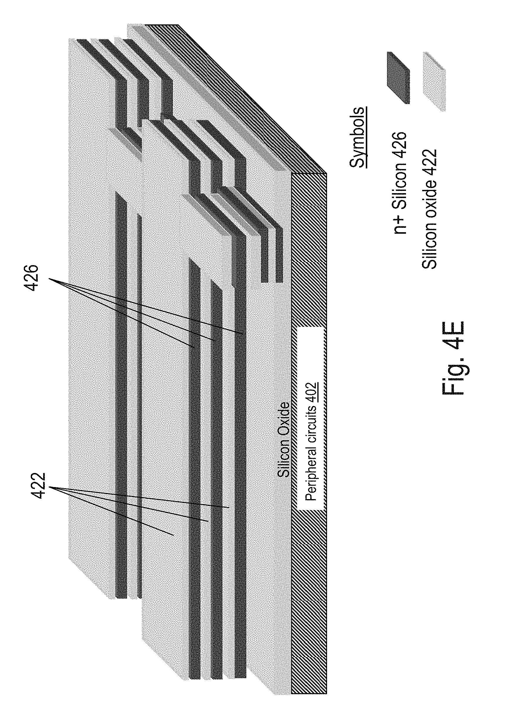
D00026
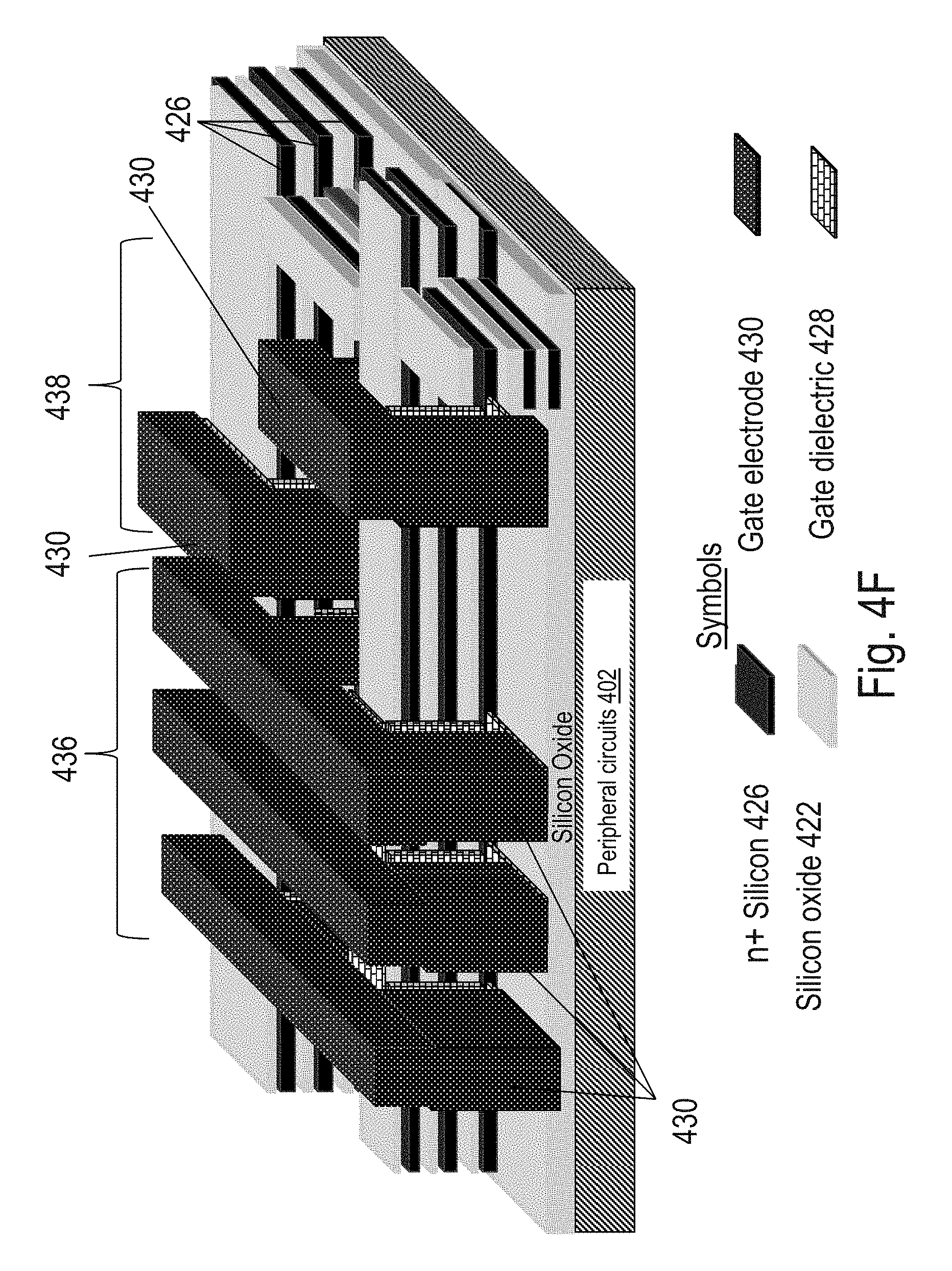
D00027

D00028

D00029

D00030

D00031

D00032

D00033
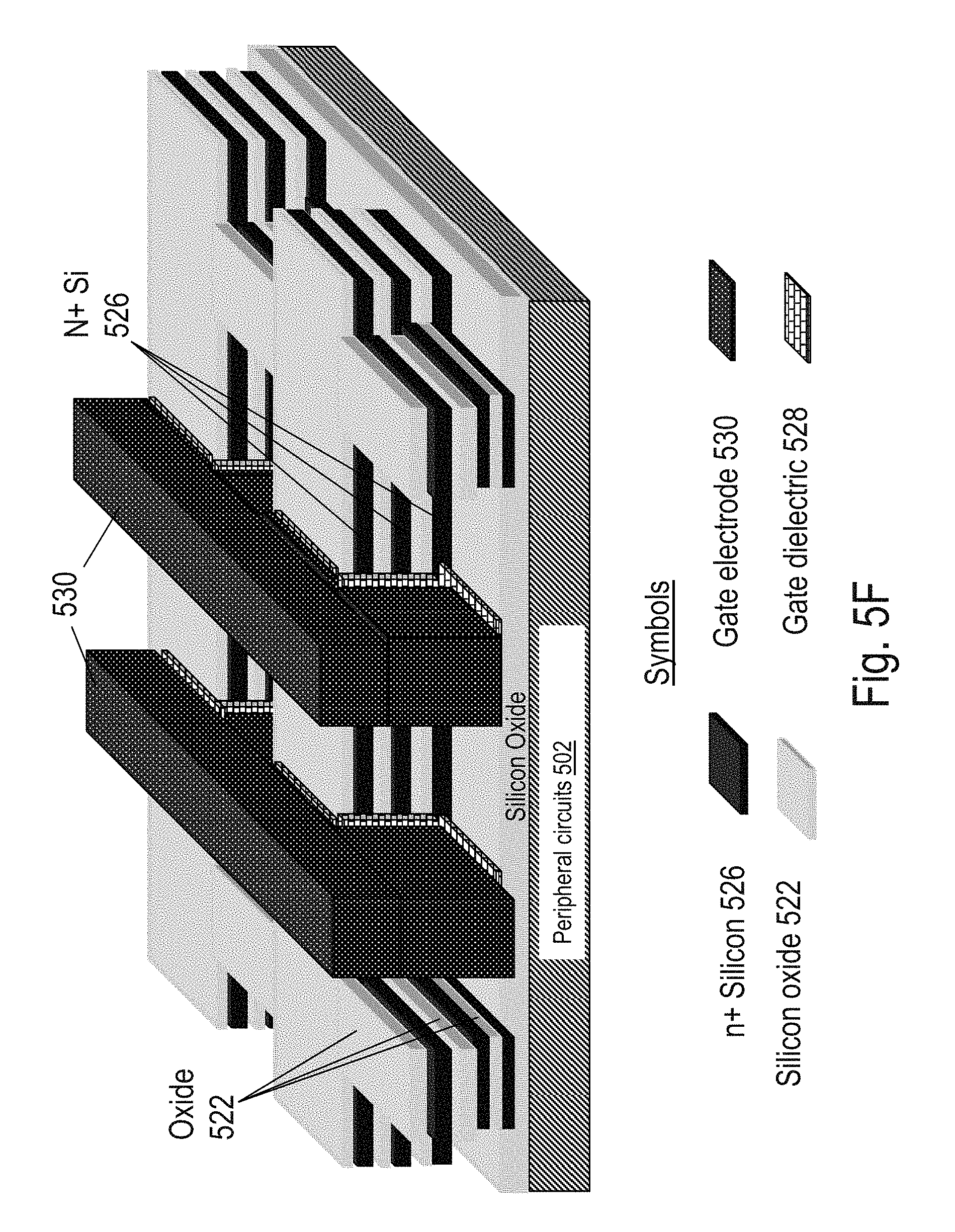
D00034

D00035

D00036

D00037

D00038

D00039
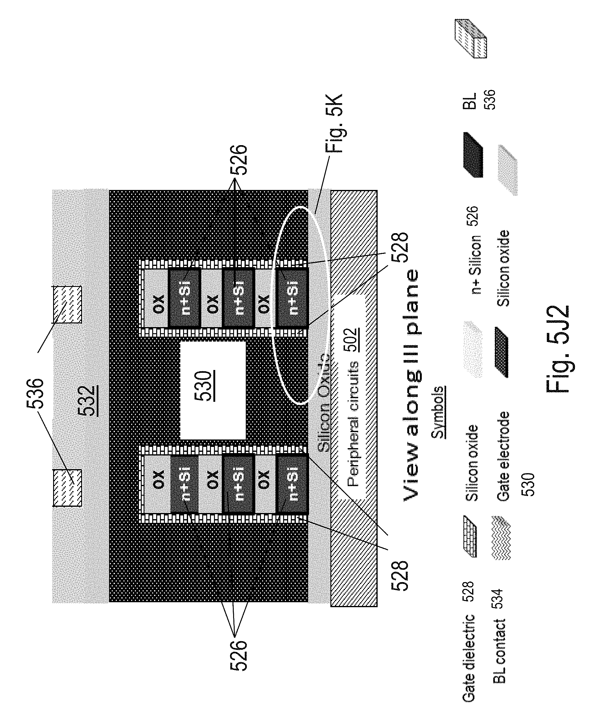
D00040

D00041
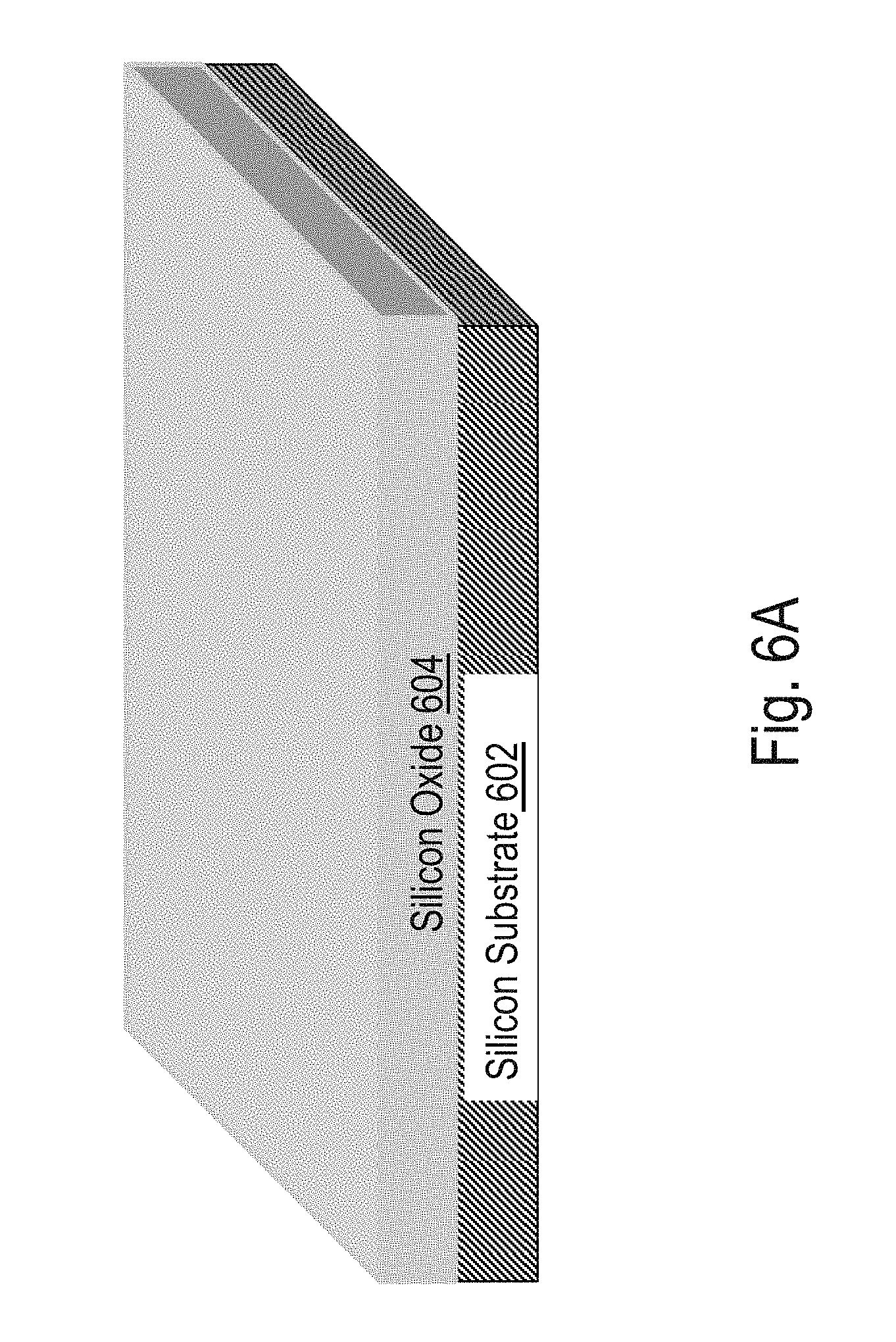
D00042

D00043

D00044
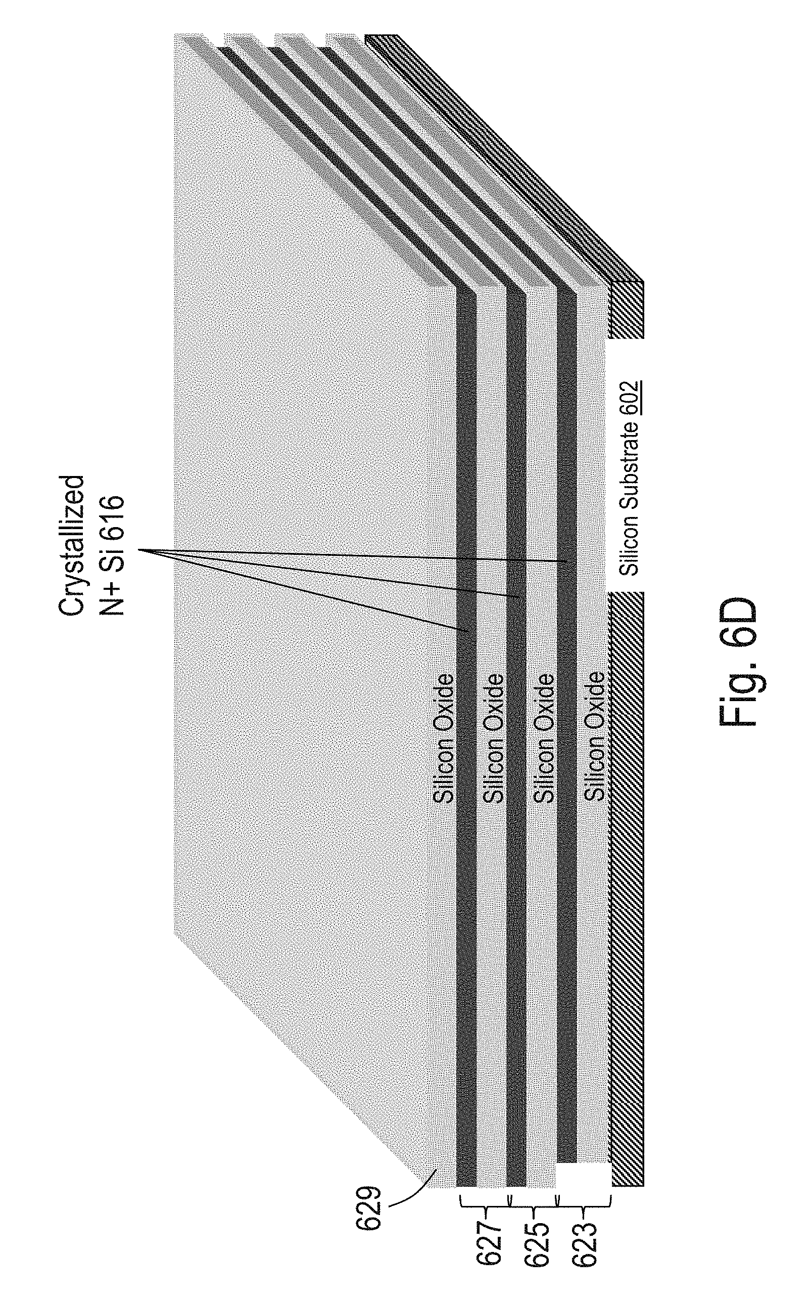
D00045

D00046

D00047

D00048
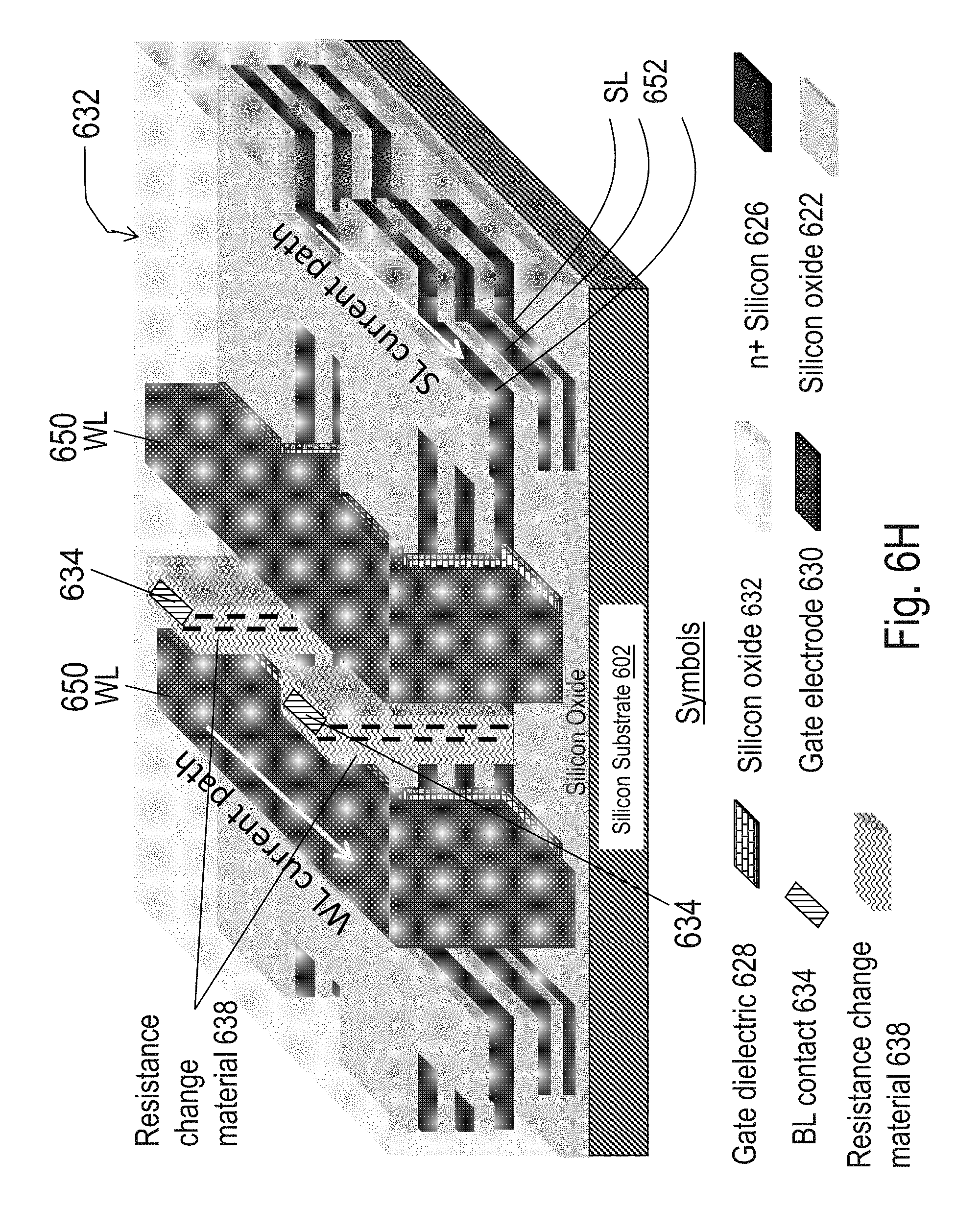
D00049

D00050

XML
uspto.report is an independent third-party trademark research tool that is not affiliated, endorsed, or sponsored by the United States Patent and Trademark Office (USPTO) or any other governmental organization. The information provided by uspto.report is based on publicly available data at the time of writing and is intended for informational purposes only.
While we strive to provide accurate and up-to-date information, we do not guarantee the accuracy, completeness, reliability, or suitability of the information displayed on this site. The use of this site is at your own risk. Any reliance you place on such information is therefore strictly at your own risk.
All official trademark data, including owner information, should be verified by visiting the official USPTO website at www.uspto.gov. This site is not intended to replace professional legal advice and should not be used as a substitute for consulting with a legal professional who is knowledgeable about trademark law.