Circuit boards and electronic packages with embedded tamper-respondent sensor
Brodsky , et al. A
U.S. patent number 10,378,925 [Application Number 16/162,679] was granted by the patent office on 2019-08-13 for circuit boards and electronic packages with embedded tamper-respondent sensor. This patent grant is currently assigned to INTERNATIONAL BUSINESS MACHINES CORPORATION. The grantee listed for this patent is INTERNATIONAL BUSINESS MACHINES CORPORATION. Invention is credited to William L. Brodsky, Silvio Dragone, Roger S. Krabbenhoft, David C. Long, Stefano S. Oggioni, Michael T. Peets, William Santiago-Fernandez.


View All Diagrams
| United States Patent | 10,378,925 |
| Brodsky , et al. | August 13, 2019 |
Circuit boards and electronic packages with embedded tamper-respondent sensor
Abstract
Electronic circuits, electronic packages, and methods of fabrication are provided. The electronic circuit includes a multilayer circuit board, and a tamper-respondent sensor embedded within the circuit board. The tamper-respondent sensor defines, at least in part, a secure volume associated with the multilayer circuit board. In certain implementations, the tamper-respondent sensor includes multiple tamper-respondent layers embedded within the circuit board including, for instance, one or more tamper-respondent frames and one or more tamper-respondent mat layers, with the tamper-respondent frame(s) being disposed, at least in part, above the tamper-respondent mat layer(s), which together define the secure volume where extending into the multilayer circuit board. In certain embodiments, one or more of the tamper-respondent layers are divided into multiple, separate tamper-respondent circuit zones, with the tamper-respondent layers, including the circuit zones, being electrically connected to monitor circuitry within the secure volume.
| Inventors: | Brodsky; William L. (Binghamtom, NY), Dragone; Silvio (Olten, CH), Krabbenhoft; Roger S. (Rochester, MN), Long; David C. (Wappingers Falls, NY), Oggioni; Stefano S. (Milan, IT), Peets; Michael T. (Staatsburg, NY), Santiago-Fernandez; William (Poughkeepsie, NY) | ||||||||||
|---|---|---|---|---|---|---|---|---|---|---|---|
| Applicant: |
|
||||||||||
| Assignee: | INTERNATIONAL BUSINESS MACHINES
CORPORATION (Armonk, NY) |
||||||||||
| Family ID: | 58386173 | ||||||||||
| Appl. No.: | 16/162,679 | ||||||||||
| Filed: | October 17, 2018 |
Prior Publication Data
| Document Identifier | Publication Date | |
|---|---|---|
| US 20190049269 A1 | Feb 14, 2019 | |
Related U.S. Patent Documents
| Application Number | Filing Date | Patent Number | Issue Date | ||
|---|---|---|---|---|---|
| 14941908 | Nov 16, 2015 | ||||
| 14865610 | Sep 25, 2015 | ||||
| Current U.S. Class: | 1/1 |
| Current CPC Class: | G01D 5/16 (20130101); H05K 3/30 (20130101); H05K 1/0298 (20130101); H05K 1/182 (20130101); H05K 3/32 (20130101); H05K 1/0275 (20130101); H05K 2201/09263 (20130101); H05K 2201/10151 (20130101); H05K 2201/096 (20130101); H05K 2201/10371 (20130101) |
| Current International Class: | H05K 1/02 (20060101); H05K 3/30 (20060101); H05K 1/18 (20060101); G01D 5/16 (20060101); H05K 3/32 (20060101) |
References Cited [Referenced By]
U.S. Patent Documents
| 3165569 | January 1965 | Bright et al. |
| 4097894 | June 1978 | Tanner et al. |
| 4160503 | July 1979 | Ohlbach |
| 4211324 | July 1980 | Ohlbach |
| 4324823 | April 1982 | Ray, III |
| 4450504 | May 1984 | Severson |
| 4496900 | January 1985 | Di Stefano et al. |
| 4516679 | May 1985 | Simpson |
| 4542337 | September 1985 | Rausch |
| 4593384 | June 1986 | Kleinjne |
| 4609104 | September 1986 | Kasper et al. |
| 4653252 | March 1987 | Van de Haar et al. |
| 4677809 | July 1987 | Long et al. |
| 4691350 | September 1987 | Kleijne et al. |
| 4807284 | February 1989 | Kleijne |
| 4811288 | March 1989 | Kleijne et al. |
| 4847139 | July 1989 | Wolf et al. |
| 4860351 | August 1989 | Weingart |
| 4865197 | September 1989 | Craig |
| 5009311 | April 1991 | Schenk |
| 5027397 | June 1991 | Double et al. |
| 5060114 | October 1991 | Feinberg et al. |
| 5075822 | December 1991 | Baumler et al. |
| 5117457 | May 1992 | Comerford et al. |
| 5159629 | October 1992 | Double et al. |
| 5185717 | February 1993 | Mori |
| 5201868 | April 1993 | Johnson |
| 5201879 | April 1993 | Steele et al. |
| 5211618 | May 1993 | Stoltz |
| 5239664 | August 1993 | Verrier et al. |
| 5243162 | September 1993 | Kobayashi |
| 5389738 | February 1995 | Piosenka et al. |
| 5406630 | April 1995 | Piosenka et al. |
| 5458912 | October 1995 | Camilletti et al. |
| 5506566 | April 1996 | Oldfield et al. |
| 5568124 | October 1996 | Joyce et al. |
| 5594439 | January 1997 | Swanson |
| 5675319 | October 1997 | Rivenberg et al. |
| 5715652 | February 1998 | Stahlecker |
| 5761054 | June 1998 | Kuhn |
| 5813113 | September 1998 | Stewart et al. |
| 5858500 | January 1999 | MacPherson |
| 5880523 | March 1999 | Candelore |
| 5975420 | November 1999 | Gogami et al. |
| 5988510 | November 1999 | Tuttle et al. |
| 6121544 | September 2000 | Petsinger |
| 6195267 | February 2001 | MacDonald, Jr. et al. |
| 6201296 | March 2001 | Fries et al. |
| 6233339 | May 2001 | Kawano et al. |
| 6259363 | July 2001 | Payne |
| 6261215 | July 2001 | Imer |
| 6301096 | October 2001 | Wozniczka |
| 6355316 | March 2002 | Miller et al. |
| 6384397 | May 2002 | Takiar et al. |
| 6396400 | May 2002 | Epstein, III et al. |
| 6420971 | July 2002 | Leck et al. |
| 6424954 | July 2002 | Leon |
| 6438825 | August 2002 | Kuhm |
| 6469625 | October 2002 | Tomooka |
| 6473995 | November 2002 | Miyakawa et al. |
| 6512454 | January 2003 | Miglioli et al. |
| 6686539 | February 2004 | Farquhar et al. |
| 6746960 | June 2004 | Goodman et al. |
| 6798660 | September 2004 | Moss et al. |
| 6817204 | November 2004 | Bash et al. |
| 6853093 | February 2005 | Cohen |
| 6879032 | April 2005 | Rosenau et al. |
| 6895509 | May 2005 | Clark |
| 6929900 | August 2005 | Farquhar et al. |
| 6946960 | September 2005 | Sisson et al. |
| 6957345 | October 2005 | Cesana et al. |
| 6970360 | November 2005 | Sinha |
| 6982642 | January 2006 | Cesana et al. |
| 6985362 | January 2006 | Mori et al. |
| 6991961 | January 2006 | Hubbard et al. |
| 6996953 | February 2006 | Perreault et al. |
| 7005733 | February 2006 | Kommerling et al. |
| 7007171 | February 2006 | Butturini et al. |
| 7015823 | March 2006 | Gillen et al. |
| 7054162 | May 2006 | Benson et al. |
| 7057896 | June 2006 | Matsuo et al. |
| 7094143 | August 2006 | Wolm et al. |
| 7094459 | August 2006 | Takahashi |
| 7095615 | August 2006 | Nichols |
| 7156233 | January 2007 | Clark et al. |
| 7180008 | February 2007 | Heitmann et al. |
| 7189360 | March 2007 | Ho et al. |
| 7214874 | May 2007 | Dangler et al. |
| 7247791 | July 2007 | Kulpa |
| 7304373 | December 2007 | Taggart et al. |
| 7310737 | December 2007 | Patel et al. |
| 7465887 | December 2008 | Suzuki et al. |
| 7475474 | January 2009 | Heitmann et al. |
| 7515418 | April 2009 | Straznicky et al. |
| 7549064 | June 2009 | Elbert et al. |
| 7640658 | January 2010 | Pham et al. |
| 7643290 | January 2010 | Narasimhan et al. |
| 7663883 | February 2010 | Shirakami et al. |
| 7671324 | March 2010 | Fleischman et al. |
| 7672129 | March 2010 | Ouyang et al. |
| 7731517 | June 2010 | Lee et al. |
| 7746657 | June 2010 | Oprea et al. |
| 7760086 | July 2010 | Hunter et al. |
| 7768005 | August 2010 | Condorelli et al. |
| 7783994 | August 2010 | Ball et al. |
| 7787256 | August 2010 | Chan et al. |
| 7868411 | January 2011 | Eaton et al. |
| 7898413 | March 2011 | Hsu et al. |
| 7901977 | March 2011 | Angelopoulos et al. |
| 7947911 | May 2011 | Pham et al. |
| 7978070 | July 2011 | Hunter |
| 8006101 | August 2011 | Crawford |
| 8084855 | December 2011 | Lower et al. |
| 8094450 | January 2012 | Cole et al. |
| 8101267 | January 2012 | Samuels et al. |
| 8133621 | March 2012 | Wormald et al. |
| 8199506 | June 2012 | Janik et al. |
| 8287336 | October 2012 | Dangler et al. |
| 8325486 | December 2012 | Arshad et al. |
| 8345423 | January 2013 | Campbell et al. |
| 8393918 | March 2013 | Cheng et al. |
| 8516269 | August 2013 | Hamlet et al. |
| 8589703 | November 2013 | Lee et al. |
| 8646108 | February 2014 | Shiakallis et al. |
| 8659506 | February 2014 | Nomizo |
| 8659908 | February 2014 | Adams et al. |
| 8664047 | March 2014 | Lower et al. |
| 8716606 | May 2014 | Kelley et al. |
| 8797059 | August 2014 | Boday et al. |
| 8836509 | September 2014 | Lowy |
| 8853839 | October 2014 | Gao et al. |
| 8879266 | November 2014 | Jarvis et al. |
| 8890298 | November 2014 | Buer et al. |
| 8947889 | February 2015 | Kelley et al. |
| 8961280 | February 2015 | Dangler et al. |
| 9003199 | April 2015 | Dellmo et al. |
| 9011762 | April 2015 | Seppa et al. |
| 9052070 | June 2015 | Davis et al. |
| 9166586 | October 2015 | Carapelli et al. |
| 9298956 | March 2016 | Wade et al. |
| 9554477 | January 2017 | Brodsky et al. |
| 9555606 | January 2017 | Fisher et al. |
| 9560737 | January 2017 | Issacs et al. |
| 9578735 | February 2017 | Fisher et al. |
| 9578764 | February 2017 | Fisher et al. |
| 9586857 | March 2017 | Cabral, Jr. et al. |
| 9591776 | March 2017 | Brodsky et al. |
| 9661747 | May 2017 | Brodsky et al. |
| 9681649 | June 2017 | Busby et al. |
| 9717154 | July 2017 | Brodsky et al. |
| 9858776 | January 2018 | Busby et al. |
| 9877383 | January 2018 | Brodsky et al. |
| 9881880 | January 2018 | Busby et al. |
| 9894749 | February 2018 | Brodsky et al. |
| 9904811 | February 2018 | Campbell et al. |
| 9911012 | March 2018 | Brodsky et al. |
| 9913362 | March 2018 | Brodsky et al. |
| 9913370 | March 2018 | Busby et al. |
| 9913416 | March 2018 | Fisher et al. |
| 9916744 | March 2018 | Busby et al. |
| 9924591 | March 2018 | Brodsky et al. |
| 9930768 | March 2018 | Fisher et al. |
| 9936573 | April 2018 | Brodsky et al. |
| 9949357 | April 2018 | Fisher et al. |
| 9978231 | May 2018 | Isaacs |
| 9999124 | June 2018 | Busby et al. |
| 2001/0049021 | December 2001 | Valimont |
| 2001/0050425 | December 2001 | Beroz et al. |
| 2001/0056542 | December 2001 | Cesana et al. |
| 2002/0002683 | January 2002 | Benson |
| 2002/0068384 | June 2002 | Beroz et al. |
| 2002/0084090 | July 2002 | Farquhar |
| 2003/0009683 | January 2003 | Schwenck et al. |
| 2003/0009684 | January 2003 | Schwenck et al. |
| 2003/0198022 | October 2003 | Ye et al. |
| 2004/0218366 | November 2004 | Speigl |
| 2005/0068735 | March 2005 | Fissore et al. |
| 2005/0111194 | May 2005 | Sohn et al. |
| 2005/0161253 | July 2005 | Heitmann et al. |
| 2005/0180104 | August 2005 | Olesen et al. |
| 2006/0034731 | February 2006 | Lewis et al. |
| 2006/0049941 | March 2006 | Hunter et al. |
| 2006/0072288 | April 2006 | Stewart et al. |
| 2006/0080348 | April 2006 | Cesana et al. |
| 2006/0196945 | September 2006 | Mendels |
| 2006/0218779 | October 2006 | Ooba et al. |
| 2007/0038865 | February 2007 | Oggioni et al. |
| 2007/0064396 | March 2007 | Oman et al. |
| 2007/0064399 | March 2007 | Mandel et al. |
| 2007/0108619 | May 2007 | Hsu |
| 2007/0125867 | June 2007 | Oberle |
| 2007/0211436 | September 2007 | Robinson et al. |
| 2007/0223165 | September 2007 | Itri et al. |
| 2007/0230127 | October 2007 | Peugh et al. |
| 2007/0268671 | November 2007 | Brandenburg et al. |
| 2007/0271544 | November 2007 | Engstrom |
| 2008/0036598 | February 2008 | Oggioni |
| 2008/0050512 | February 2008 | Lower et al. |
| 2008/0061972 | March 2008 | Hwang et al. |
| 2008/0086876 | April 2008 | Douglas |
| 2008/0128897 | June 2008 | Chao |
| 2008/0144290 | June 2008 | Brandt et al. |
| 2008/0159539 | July 2008 | Huang et al. |
| 2008/0160274 | July 2008 | Dang et al. |
| 2008/0191174 | August 2008 | Ehrensvard et al. |
| 2008/0251906 | October 2008 | Eaton |
| 2008/0278353 | November 2008 | Smith et al. |
| 2009/0031135 | January 2009 | Kothandaraman |
| 2009/0073659 | March 2009 | Peng et al. |
| 2009/0152339 | June 2009 | Hawkins et al. |
| 2009/0166065 | July 2009 | Clayton et al. |
| 2009/0212945 | August 2009 | Steen |
| 2010/0088528 | April 2010 | Sion |
| 2010/0110647 | May 2010 | Hiew et al. |
| 2010/0134959 | June 2010 | Fife et al. |
| 2010/0177487 | July 2010 | Arshad et al. |
| 2010/0319986 | December 2010 | Bleau et al. |
| 2011/0001237 | January 2011 | Brun et al. |
| 2011/0038123 | February 2011 | Janik et al. |
| 2011/0103027 | May 2011 | Aoki et al. |
| 2011/0241446 | October 2011 | Tucholski |
| 2011/0299244 | December 2011 | Dede et al. |
| 2012/0047374 | February 2012 | Klum et al. |
| 2012/0050998 | March 2012 | Klum et al. |
| 2012/0052252 | March 2012 | Kohli et al. |
| 2012/0068846 | March 2012 | Dalzell et al. |
| 2012/0117666 | May 2012 | Oggioni et al. |
| 2012/0140421 | June 2012 | Kirstine et al. |
| 2012/0319986 | June 2012 | Toh et al. |
| 2012/0170217 | July 2012 | Nishikimi et al. |
| 2012/0185636 | July 2012 | Leon et al. |
| 2012/0244742 | September 2012 | Wertz et al. |
| 2012/0256305 | October 2012 | Kaufmann et al. |
| 2012/0320529 | December 2012 | Loong et al. |
| 2013/0021758 | January 2013 | Bernstein et al. |
| 2013/0033818 | February 2013 | Hosoda et al. |
| 2013/0058052 | March 2013 | Arshad et al. |
| 2013/0104252 | April 2013 | Yanamadala et al. |
| 2013/0141137 | June 2013 | Krutzik et al. |
| 2013/0154834 | June 2013 | Busca et al. |
| 2013/0158936 | June 2013 | Rich et al. |
| 2013/0208422 | August 2013 | Hughes et al. |
| 2013/0235527 | September 2013 | Wagner et al. |
| 2013/0283386 | October 2013 | Lee |
| 2014/0022733 | January 2014 | Lim et al. |
| 2014/0027159 | January 2014 | Salle et al. |
| 2014/0028335 | January 2014 | Salle et al. |
| 2014/0033331 | January 2014 | Salle et al. |
| 2014/0160679 | June 2014 | Kelty et al. |
| 2014/0184263 | July 2014 | Ehrenpfordt et al. |
| 2014/0204533 | July 2014 | Abeyasekera et al. |
| 2014/0206800 | July 2014 | Wu et al. |
| 2014/0233165 | August 2014 | Farkas et al. |
| 2014/0296410 | October 2014 | Cheng et al. |
| 2014/0306014 | October 2014 | Salle et al. |
| 2014/0321064 | October 2014 | Bose et al. |
| 2014/0325688 | October 2014 | Cashin |
| 2015/0007427 | January 2015 | Dangler et al. |
| 2015/0120072 | April 2015 | Marom et al. |
| 2015/0143551 | May 2015 | Tiemeijer |
| 2015/0163933 | June 2015 | Steiner |
| 2015/0213243 | July 2015 | Hughes et al. |
| 2015/0235053 | August 2015 | Lee et al. |
| 2015/0244374 | August 2015 | Hadley |
| 2015/0307250 | October 2015 | Sokol |
| 2016/0005262 | January 2016 | Hirato et al. |
| 2016/0012693 | January 2016 | Sugar |
| 2016/0262270 | September 2016 | Isaacs et al. |
| 2017/0006712 | January 2017 | Matsushima et al. |
| 2017/0019987 | March 2017 | Dragone et al. |
| 2017/0068881 | March 2017 | Camper et al. |
| 2017/0089729 | March 2017 | Brodsky et al. |
| 2017/0089977 | March 2017 | Warnock et al. |
| 2017/0091491 | March 2017 | Dangler et al. |
| 2017/0094783 | March 2017 | Dangler et al. |
| 2017/0094803 | March 2017 | Dangler et al. |
| 2017/0094804 | March 2017 | Brodsky et al. |
| 2017/0094805 | March 2017 | Dangler et al. |
| 2017/0094808 | March 2017 | Brodsky et al. |
| 2017/0103683 | April 2017 | Yazdi et al. |
| 2017/0108543 | April 2017 | Brodsky et al. |
| 2017/0111998 | April 2017 | Brodsky et al. |
| 2017/0156223 | June 2017 | Fisher et al. |
| 2017/0171999 | June 2017 | Fisher et al. |
| 2017/0286725 | October 2017 | Lewis |
| 2018/0061196 | March 2018 | Busby et al. |
| 2018/0070444 | March 2018 | Brodsky et al. |
| 2018/0082556 | March 2018 | Dragone et al. |
| 2018/0092203 | March 2018 | Dragone et al. |
| 2018/0092204 | March 2018 | Dragone et al. |
| 2018/0096173 | April 2018 | Brodsky et al. |
| 2018/0098423 | April 2018 | Brodsky et al. |
| 2018/0098424 | April 2018 | Busby et al. |
| 2018/0102329 | April 2018 | Busby et al. |
| 2018/0103537 | April 2018 | Brodsky et al. |
| 2018/0103538 | April 2018 | Brodsky et al. |
| 2018/0107848 | April 2018 | Campbell et al. |
| 2018/0108229 | April 2018 | Busby et al. |
| 2018/0110142 | April 2018 | Fisher et al. |
| 2018/0110165 | April 2018 | Fisher et al. |
| 2018/0235081 | August 2018 | Brodsky et al. |
| 2014-30639 | Mar 2010 | CN | |||
| 10-4346587 | Feb 2015 | CN | |||
| 19816571 | Oct 1999 | DE | |||
| 19816572 | Oct 1999 | DE | |||
| 10-2012-203955 | Sep 2013 | DE | |||
| 0 056 360 | Oct 1993 | EP | |||
| 0 629 497 | Dec 1994 | EP | |||
| 1 734 578 | Dec 2006 | EP | |||
| 1 968 362 | Sep 2008 | EP | |||
| 2 104 407 | Sep 2009 | EP | |||
| 1 672 464 | Apr 2012 | EP | |||
| 2 560 467 | Feb 2013 | EP | |||
| 61-297035 | Dec 1986 | JP | |||
| 2000-238141 | Sep 2000 | JP | |||
| 2007-173416 | Jul 2007 | JP | |||
| 2007-305761 | Nov 2007 | JP | |||
| 2013-125807 | Jun 2013 | JP | |||
| 2013-140112 | Jul 2013 | JP | |||
| WO 1999/003675 | Jan 1999 | WO | |||
| WO 1999/021142 | Apr 1999 | WO | |||
| WO 2001/063994 | Aug 2001 | WO | |||
| WO 2003/012606 | Feb 2003 | WO | |||
| WO 2003/025080 | Mar 2003 | WO | |||
| WO 2004/040505 | May 2004 | WO | |||
| WO 2009/042335 | Apr 2009 | WO | |||
| WO 2009/092472 | Jul 2009 | WO | |||
| WO 2010/128939 | Nov 2010 | WO | |||
| WO 2013/004292 | Jan 2013 | WO | |||
| WO 2013/189483 | Dec 2013 | WO | |||
| WO 2014/086987 | Jun 2014 | WO | |||
| WO 2014/158159 | Oct 2014 | WO | |||
Other References
|
Holm, Ragnar, "Electric Contacts: Theory and Application", Spinger-Verlag, New York, 4th Edition, 1981 (pp. 10-19). cited by applicant . Clark, Andrew J., "Physical Protection of Cryptographic Devices", Advanced in Cyprtology, Eurocrypt '87, Springer, Berlin Heidelberg (1987) (11 pages). cited by applicant . Halperin et al., "Latent Open Testing of Electronic Packaging", MCMC-194, IEEE (1994) (pp. 83-33). cited by applicant . Simek, Bob, "Tamper Restrictive Thermal Ventilation System for Enclosures Requiring Ventilation and Physical Security", IBM Publication No. IPCOM000008607D, Mar. 1, 1998 (2 pages). cited by applicant . NIST, "Security Requirements for Cryptographic Modules", FIPS Pub. 140-2, Issued May 25, 2001. cited by applicant . Pamula et al., "Cooling of Integrated Circuits Using Droplet-Based Microfluidics", Association for Computing Machinery (ACM), GLSVLSI'03, Apr. 28-29, 2003 (pp. 84-87). cited by applicant . Saran et al., "Fabrication and Characterization of Thin Films of Single-Walled Carbon Nanotube Bundles on Flexible Plastic Substrates", Journal of the American Chemical Society, vol. 126, No. 14 (Mar. 23, 2004) (pp. 4462-4463). cited by applicant . Khanna P.K. et al., "Studies on Three-Dimensional Moulding, Bonding and Assembling of Low-Temperature-Cofired Ceramics MEMS and MST Applications." Materials Chemistry and Physics, vol. 89, No. 1 (2005) (pp. 72-79). cited by applicant . Drimer et al., "Thinking Inside the Box: System-Level Failures of Tamper Proofing", 2008 IEEE Symposium on Security and Privacy, (Feb. 2008) (pp. 281-295). cited by applicant . Loher et al., "Highly Integrated Flexible Electronic Circuits and Modules", 3rd International IEEE on Microsystems, Packaging, Assembly & Circuits Technology Conference (Oct. 22-24, 2008) (Abstract Only) (1 page). cited by applicant . Sample et al., "Design of an RFID-Based Battery-Free Programmable Sensing Platform", IEEE Transactions on Instrumentation and Measurement, vol. 57, No. 11, Nov. 2008 (pp. 2608-2615). cited by applicant . Jhang et al., "Nonlinear Ultrasonic Techniques for Non-Destructive Assessment of Micro Damage in Material: A Review", International Journal of Prec. Eng. & Manuf., vol. 10, No. 1, Jan. 2009 (pp. 123-135). cited by applicant . Anonymous, "Consolidated Non-Volatile Memory in a Chip Stack", IBM Technical Disclosure: IP.com No. IPCOM000185250, Jul. 16, 2009 (6 pages). cited by applicant . Isaacs et al., "Tamper Proof, Tamper Evident Encryption Technology", Pan Pacific Symposium SMTA Proceedings (2013) (9 pages). cited by applicant . Wikipedia, "Toughened Glass", http://web.archive.org/web/20140605093019/https://en.wikipedia.org/wiki/t- oughened_glass, downloaded/printed Jun. 5, 2014 (4 pages). cited by applicant . Anonymous, "Selective Memory Encryption", IBM Technical Disclosure: IP.com IPCOM000244183, Nov. 20, 2015 (6 pages). cited by applicant . Zhou et al., "Nonlinear Analysis for Hardware Trojan Detection", ICSPCC2015, IEEE (2015) (4 pages). cited by applicant . Harting Mitronics, "Saftey Caps for Payment Terminals", http://harting-mitronics.ch/fileadmin/hartingmitronics/case_studies/Safte- y_caps_for_payment_terminals.pdf, downloaded Aug. 2016 (2 pages). cited by applicant . Gold Phoenix Printed Circuit Board, "Why multilayer pcb is used so widely?", May 7, 2012, accessed online @ [http://www.goldphoenixpcb.com/html/Support_Resource/others/arc_110.html] on Feb. 15, 2017. cited by applicant . Busby et al., "Enclosure-to-Board Interface with Tamper-Detect Circuit(s)", U.S. Appl. No. 15/901,985, filed Feb. 22, 2018 (59 pages). cited by applicant . Brodsky et al., "Tamper-Respondent Sensors with Liquid Crystal Polymer Layers", U.S. Appl. No. 15/944,898, filed Apr. 4, 2018 (59 pages). cited by applicant . Busby et al., "Tamper-Proof Electronic Packages with Stressed Glass Component Substrate(s)", U.S. Appl. No. 16/045,868, filed Jul. 26, 2018 (53 pages. cited by applicant . Busby et al., "Tamper-Proof Electronic Packages with Stressed Glass Component Substrate(s)", U.S. Appl. No. 16/045,880, filed Jul. 26, 2018 (55 pages). cited by applicant . Busby et al., "Multi-Layer Stack with Embedded Tamper-Detect Protection", U.S. Appl. No. 16/048,622, filed Jul. 30, 2018 (64 pages). cited by applicant . Busby et al., "Multi-Layer Stack with Embedded Tamper-Detect Protection", U.S. Appl. No. 16/048,634, filed Jul. 30, 2018 (65 pages). cited by applicant . Busby et al., "Multi-Layer Stack with Embedded Tamper-Detect Protection", U.S. Appl. No. 16/048,650, filed Jul. 30, 2018 (68 pages). cited by applicant . Brodsky et al., "Circuit Boards and Electronic Packages with Embedded Tamper-Respondent Sensor", U.S. Appl. No. 16/136,589, filed Sep. 20, 2018 (45 pages). cited by applicant . Brodsky et al., "List of IBM Patents and Patent Applications Treated as Related", U.S. Appl. No. 16/162,679, filed Oct. 17, 2018, dated Oct. 17, 2018 (3 pages). cited by applicant. |
Primary Examiner: Phan; Minh Q
Attorney, Agent or Firm: Poltavets, Esq.; Tihon Radigan, Esq.; Kevin P. Heslin Rothenberg Farley & Mesiti P.C.
Claims
What is claimed is:
1. A method of fabricating an electronic circuit comprising: providing a multilayer circuit board, the multilayer circuit board being a single circuit board formed of multiple layers; and disposing at least one electronic component on an uppermost surface of the multilayer circuit board, the multilayer circuit board including a continuous groove formed in the uppermost surface of the multilayered circuit board to facilitate attaching an enclosure to the multilayer circuit board, the at least one electronic component being within a surface area of the uppermost surface encircled by the continuous groove; providing a tamper-respondent sensor embedded within the multilayer circuit board, the tamper-respondent sensor defining, at least in part, a secure volume associated with the multilayer circuit board, and comprising: multiple tamper-respondent layers within the multilayer circuit board, the multiple tamper-respondent layers being spaced apart, parallel layers within the multilayer circuit board that facilitate defining the secure volume, at least in part, within the multilayer circuit board, and the multiple tamper-respondent layers comprising: at least one tamper-respondent picture frame-type layer encircling the secure volume within the multilayer circuit board and disposed below the surface area of the multilayer circuit board encircled by the continuous groove, a tamper-respondent picture frame-type layer of the at least one tamper-respondent picture frame-type layer comprising one or more conductive trace lines extending horizontally around the tamper-respondent picture frame-type layer within the multilayer circuit board and encircling the secure volume within the multilayer circuit board; and at least one tamper-respondent mat layer forming a base of the secure volume within the multilayer circuit board, the at least one tamper-respondent frame layer being disposed over the at least one tamper-respondent mat layer.
2. The method of claim 1, wherein at least one tamper-respondent layer of the multiple tamper-respondent layers comprises multiple, separate tamper-respondent circuit zones, and wherein the multiple tamper-respondent layers, including the multiple, separate tamper-respondent circuit zones of the at least one tamper-respondent layer, are electrically connected to monitor circuitry within the secure volume associated with the multilayer circuit board.
3. The method of claim 1, wherein at least two tamper-respondent layers of the multiple tamper-respondent layers each comprise multiple, separate tamper-respondent circuit zones, and wherein at least two tamper-respondent circuit zones within different tamper-respondent layers of the at least two tamper-respondent layers are electrically connected to a common monitor circuit within the secure volume associated with the multilayer circuit board.
4. The method of claim 3, wherein the at least one tamper-respondent picture frame-type layer of the multiple tamper-respondent layers defines, at least in part, a side portion of the secure volume within the multilayer circuit board.
5. The method of claim 1, wherein the multilayer circuit board comprises an external signal layer embedded within the multilayer circuit board, the external signal layer electrically connecting to the at least one electronic component disposed on the multilayer circuit board within the secure volume, and residing, at least in part, over a tamper-respondent mat layer of the at least one tamper-respondent mat layer.
6. The method of claim 1, wherein the multiple tamper-respondent layers within the multilayer circuit board comprise at least two tamper-respondent picture frame-type layers, the at least two tamper-respondent picture frame-type layers defining, at least in part, a periphery of the secure volume where extending into the multilayer circuit board.
7. The method of claim 1, wherein the at least one tamper-respondent picture frame-type layer embedded within the multilayer circuit board defines a periphery of the secure volume within the multilayer circuit board.
8. The method of claim 1, wherein the one or more conductive trace lines of the tamper-respondent picture frame-type layer of the at least one tamper-respondent picture frame-type layer encircling the secure volume within the multilayer circuit board are encircled or intersected by the continuous groove in the uppermost surface of the multilayer circuit board.
9. The method of claim 8, wherein the tamper-respondent mat layer of the at least one tamper-respondent may layer extends from below the secure volume outward past the groove in the multilayer circuit board.
Description
BACKGROUND
Many activities require secure electronic communications. To facilitate secure electronic communications, an encryption/decryption system may be implemented on an electronic assembly or printed circuit board assembly that is included in equipment connected to a communications network. Such an electronic assembly is an enticing target for malefactors since it may contain codes or keys to decrypt intercepted messages, or to encode fraudulent messages. To prevent this, an electronic assembly may be mounted in an enclosure, which is then wrapped in a security sensor, and encapsulated with polyurethane resin. A security sensor may be, in one or more embodiments, a web or sheet of insulating material with circuit elements, such as closely-spaced, conductive lines fabricated on it. The circuit elements are disrupted if the sensor is torn, and the sensor can be sensed in order to generate an alarm signal. The alarm signal may be conveyed to a monitor circuit in order to reveal an attack on the integrity of the assembly. The alarm signal may also trigger an erasure of encryption/decryption keys stored within the electronic assembly.
In the above configuration, the electronic package, or tamper-proof electronic package, may be difficult to test due to the presence of the security sensor wrapped fully around the enclosure. Additionally, in this configuration it is difficult to recover components from the electronic package, for instance, should a manufacturing defect in the package be detected.
SUMMARY
Provided herein, in one or more aspects, is a method of fabricating an electronic circuit. The method includes providing a multilayer circuit board, and providing a tamper-respondent sensor embedded within the multilayer circuit board. The tamper-respondent sensor defines, at least in part, a secure volume associated with the multilayer circuit board. The tamper-respondent sensor includes multiple tamper-respondent layers within the multilayer circuit board. The multiple tamper-respondent layers are spaced apart, parallel layers within the multilayer circuit board that facilitate defining the secure volume, at least in part, within the multilayer circuit board. The multiple tamper-respondent layers include at least one tamper-respondent picture frame-type layer encircling the secure volume within the multilayer circuit board, and at least one tamper-respondent mat layer forming a base of the secure volume within the multilayer circuit board. A tamper-respondent picture frame-type layer of the at least one tamper-respondent picture frame-type layer includes one or more conductive trace lines extending horizontally within the tamper-respondent picture frame-type layer within the multilayer circuit board and encircling the secure volume within the multilayer circuit board. The at least one tamper-respondent frame layer is disposed over the at least one tamper-respondent mat layer.
Additional features and advantages are realized through the techniques of the present invention. Other embodiments and aspects of the invention are described in detail herein and are considered a part of the claimed invention.
BRIEF DESCRIPTION OF THE DRAWINGS
One or more aspects of the present invention are particularly pointed out and distinctly claimed as examples in the claims at the conclusion of the specification. The foregoing and other objects, features, and advantages of the invention are apparent from the following detailed description taken in conjunction with the accompanying drawings in which:
FIG. 1 is a partial cut-away of a conventional tamper-proof electronic package;
FIG. 2 is a cross-sectional elevational view of one embodiment of a prior art, tamper-proof electronic package comprising an electronic circuit;
FIG. 3 depicts one embodiment of a tamper-respondent trace pattern or circuit which may be employed within a tamper-respondent sensor, in accordance with one or more aspects of the present invention;
FIG. 4A is a cross-sectional elevational view of one embodiment of a tamper-proof electronic package, which includes a tamper-respondent sensor embedded within a multilayer circuit board, in accordance with one or more aspects of the present invention;
FIG. 4B is a top plan view of the multilayer circuit board of FIG. 4A, depicting one embodiment of the secure volume where defined within the multilayer circuit board, in accordance with one or more aspects of the present invention;
FIG. 5A is a partial cross-sectional elevational view of a tamper-proof electronic package comprising an electronic circuit with a multilayer circuit board and embedded tamper-respondent sensor, in accordance with one or more aspects of the present invention;
FIG. 5B is a schematic of a portion of the tamper-proof electronic package of FIG. 5A, in accordance with one or more aspects of the present invention;
FIG. 5C depicts an alternate embodiment of an electronic circuit comprising a multilayer circuit board and an embedded tamper-respondent sensor, in accordance with one or more aspects of the present invention;
FIG. 6 illustrates one embodiment of a process for fabricating a multilayer circuit board with an embedded tamper-respondent sensor, in accordance with one or more aspects of the present invention;
FIG. 7 is a plan view of one embodiment of a tamper-respondent mat layer for a tamper-respondent sensor embedded within a multilayer circuit board, in accordance with one or more aspects of the present invention;
FIG. 8A is a plan view of the tamper-respondent mat layer of FIG. 7, with conductive vias to an upper layer illustrated for electrically connecting to the conductive traces of the different circuit zones of the tamper-respondent mat layer, in accordance with one or more aspects of the present invention;
FIG. 8B is a partial plan view of the tamper-respondent mat layer of FIG. 8A, showing a portion of the conductive traces provided within two adjacent circuit zones of the tamper-respondent mat layer, in accordance with one or more aspects of the present invention;
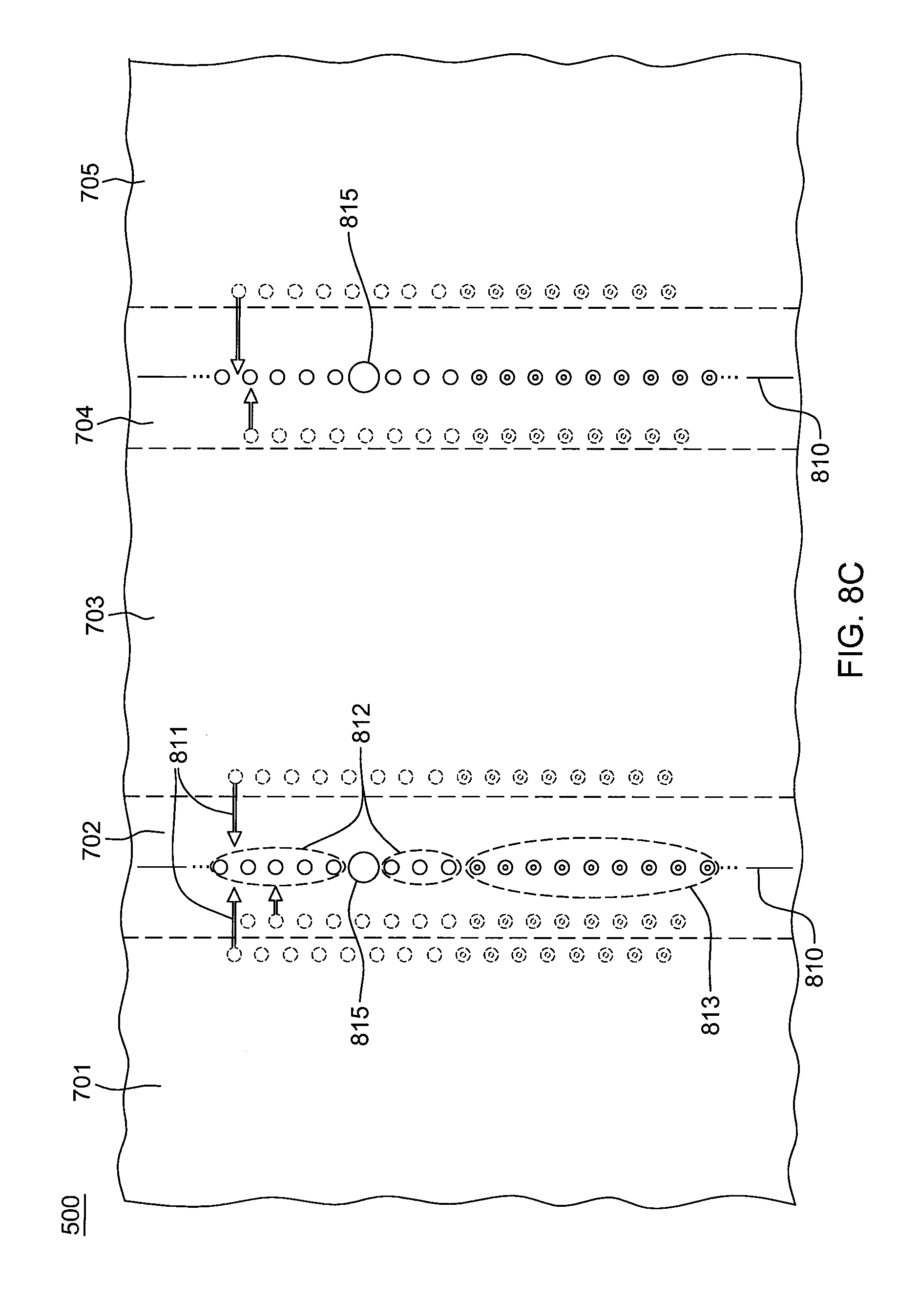
FIG. 8C is a plan view of a wiring layer overlying the tamper-respondent mat layer of FIG. 8A, and illustrating an offsetting of the conductive vias from the tamper-respondent mat layer of FIG. 8A to selected locations within the wiring layer, which also accommodate (in the depicted example) external signal line vias facilitating communication to and from the secure volume associated with the multilayer circuit board, in accordance with one or more aspects of the present invention;
FIG. 8D depicts a tamper-respondent mat layer above the wiring layer of FIG. 8C, and illustrates further offsetting of conductive vias, from one mat layer to the next, to enhance security of the tamper-respondent sensor, in accordance with one or more aspects of the present invention;
FIG. 8E is a plan view of a first tamper-respondent frame above the tamper-respondent mat layer of FIG. 8D, which facilitates defining, in part, the secure volume within the multilayer circuit board, in accordance with one or more aspects of the present invention;
FIG. 8F is a partial depiction of conductive traces for a tamper-respondent frame such as illustrated in FIG. 8E, in accordance with one or more aspects of the present invention;
FIG. 8G is a plan view of a second tamper-respondent frame overlying the first tamper-respondent frame, and further facilitating defining the secure volume in association with the multilayer circuit board, in accordance with one or more aspects of the present invention; and
FIG. 9 is a schematic illustration of one embodiment of monitor circuitry and electrical interconnection of different circuit zones of different tamper-respondent layers of the tamper-respondent sensor within the secure volume associated with the multilayer circuit board, in accordance with one or more aspects of the present invention.
DETAILED DESCRIPTION
Aspects of the present invention and certain features, advantages, and details thereof, are explained more fully below with reference to the non-limiting example(s) illustrated in the accompanying drawings. Descriptions of well-known materials, fabrication tools, processing techniques, etc., are omitted so as not to unnecessarily obscure the invention in detail. It should be understood, however, that the detailed description and the specific example(s), while indicating aspects of the invention, are given by way of illustration only, and are not by way of limitation. Various substitutions, modifications, additions, and/or arrangements, within the spirit and/or scope of the underlying inventive concepts will be apparent to those skilled in the art for this disclosure. Note further that reference is made below to the drawings, which are not drawn to scale for ease of understanding, and wherein the same reference numbers used throughout different figures designate the same or similar components.
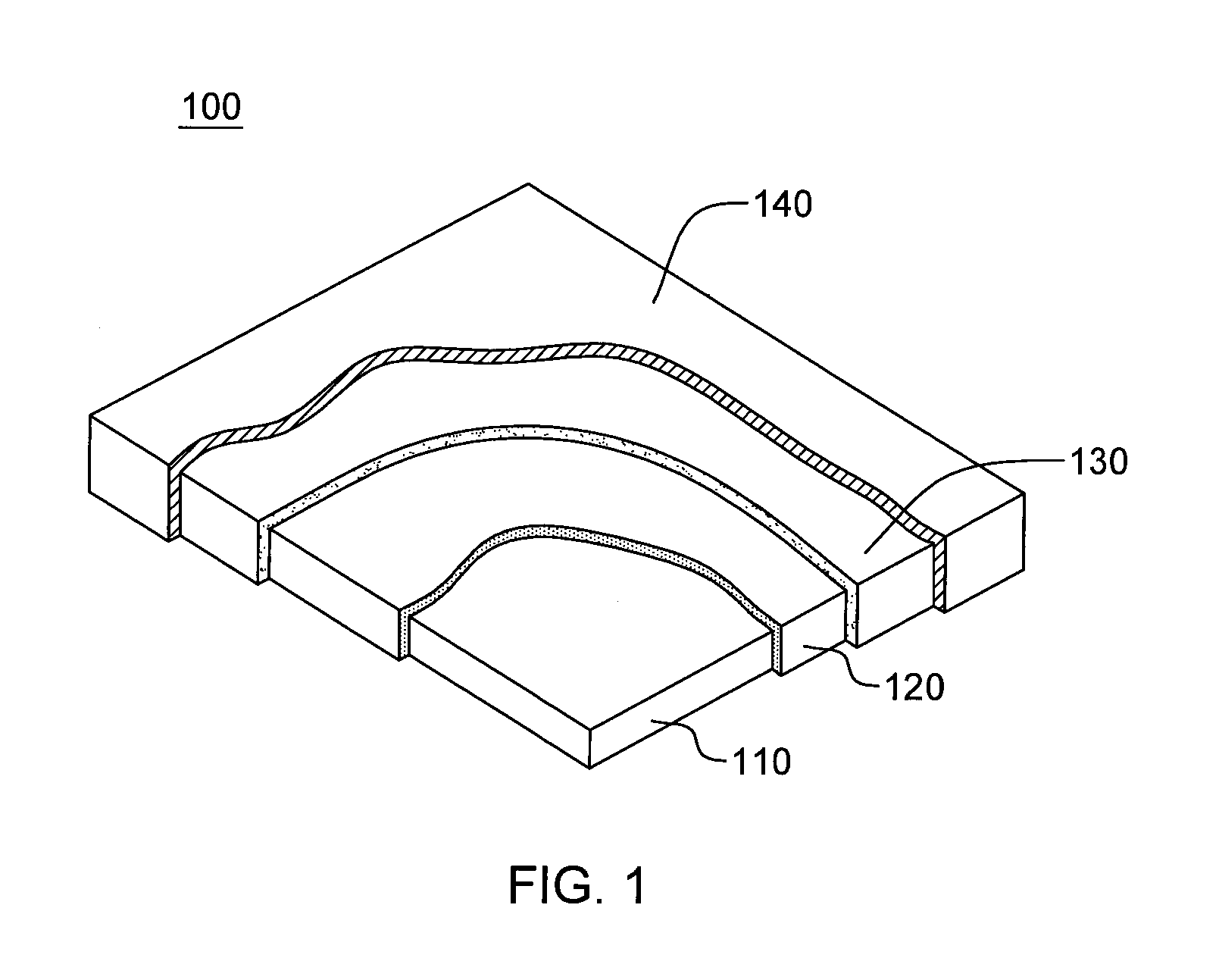
Reference is first made to FIG. 1 of the drawings, which illustrates one embodiment of an electronic package 100 configured as a tamper-proof electronic package for purposes of discussion. In the depicted embodiment, an enclosure 110 is provided containing, for instance, an electronic assembly, which in one embodiment may include a plurality of electronic components, such as an encryption module and associated memory. The encryption module may comprise security-sensitive information with, for instance, access to the information stored in the module requiring use of a variable key, and with the nature of the key being stored in the associated memory within the enclosure.
In one or more implementations, a tamper-proof electronic package such as depicted is configured or arranged to detect attempts to tamper-with or penetrate into enclosure 110. Accordingly, enclosure 110 also includes, for instance, a monitor circuit which, if tampering is detected, activates an erase circuit to erase information stored within the associated memory, as well as the encryption module within the communications card. These components may be mounted on, and interconnected by, a printed circuit board or other substrate, and be internally powered via a power supply provided within the enclosure.
In the embodiment illustrated, and as one example only, enclosure 110 is surrounded by a tamper-respondent sensor 120, an encapsulant 130, and an outer, thermally conductive enclosure 140. In one or more implementations, tamper-respondent sensor 120 may comprise a folded, tamper-respondent laminate, and encapsulant 130 may be provided in the form of a molding. Tamper-respondent sensor 120 may include various detection layers, which are monitored via a ribbon cable (discussed below) by the enclosure monitor, against sudden violent attempts to penetrate enclosure 110 and damage the enclosure monitor or erase circuit before information can be erased from the encryption module. The tamper-respondent sensor may be, for example, any such article commercially available or described in various publications and issued patents.
By way of example, tamper-respondent sensor 120 may be formed as a tamper-respondent laminate comprising a number of separate layers with, for instance, an outermost lamination-respondent layer including a matrix of diagonally-extending, semi-conductive lines printed onto a regular, thin insulating film. The matrix of lines forms a number of continuous conductors which would be broken if attempts are made to penetrate the film. The lines may be formed, for instance, by printing carbon-loaded Polymer Thick Film, PTF, ink onto the film, and selectively connecting the lines on each side, by conductive vias at the edges of the film. Connections between the lines and an enclosure monitor of the communications card may be provided via, for instance, one or more ribbon cables. The ribbon cable itself may be formed of lines of carbon-loaded ink printed onto an extension of the film, if desired. Connections between the matrix and the ribbon cable may be made via connectors formed on one edge of the film. As noted, the laminate may be folded to define the tamper-respondent sensor 120 surrounding enclosure 110.
In one or more implementations, the various elements of the laminate may be adhered together and folded around enclosure 110, in a similar manner to gift-wrapping a parcel, to define the tamper-respondent sensor 120. The assembly may be placed in a mold which is then filled with, for instance, cold-pour polyurethane, and the polyurethane may be cured and hardened to form an encapsulant 130. The encapsulant may, in one or more embodiments, completely surround the tamper-respondent sensor 120 and enclosure 110, and thus form a complete environmental seal, protecting the interior of the enclosure. The hardened polyurethane is resilient and increases robustness of the electronic package in normal use. Outer, thermally conductive enclosure 140 may optionally be provided over encapsulant 130 to, for instance, provide further structural rigidity to the electronic package.
Note that, as an enhancement, within a sealed electronic package, such as the tamper-proof electronic package depicted in FIG. 1 and described above, structures and methods for facilitating heat transfer from one or more electronic components disposed therein outwards through the enclosure and any other layers of the electronic package may be provided.
FIG. 2 depicts in detail one embodiment of a tamper-proof electronic package 200. Electronic package 200 is defined by, for instance, a base metal shell 202 and a top metal shell 204. Outer surfaces of base metal shell 202 and top metal shell 204 may be provided with dimples 206, with an electronic assembly 208 resting on dimples 206 defined in base metal shell 202. Electronic assembly 208 may include, for instance, a printed circuit board 210 with electronic components 212 that are electrically connected via conductors (not shown) defined within or on printed circuit board 210.
Hollow spacers 213 may be placed below dimples 206 in top metal shell 204, and rivets 214 provided, extending through openings in dimples 206, through hollow spacers 213 and through openings in printed circuit board 210 to base metal shell 202 in order to fixedly secure electronic assembly 208 within the enclosure formed by base and top metal shells 202, 204. A security mesh or tamper-respondent sensor 216 is wrapped around the top, base, and four sides of the enclosure formed by base and top metal shells 202, 204. As illustrated, in one or more embodiments, top metal shell 204 may have an opening through which a bus 220 extends. One end of bus 220 may be connected to conductors (not shown) on printed circuit board 210, and the other end may be connected to conductors (not shown) on a printed circuit board 222. As bus 220 passes through the opening, the bus extends between an inner edge region 223 of the security mesh 216 and an overlapping, outer edge region 224 of the security mesh 216. A group of wires 226 connect, in one embodiment, security mesh 216 to conductors on printed circuit board 210. Circuitry on printed circuit board 210 is responsive to a break in security mesh 216, in which case, an alarm signal may be emitted on bus 220, and also encryption/decryption keys stored within electronic assembly 208 may be erased.
In one or more implementations, liquid polyurethane resin may be applied to security mesh 216 and cured. An outer, thermally conductive enclosure 228, such as a copper enclosure, may be filled with liquid polyurethane resin with the electronic assembly and inner enclosure and security mesh suspended within it. Upon curing the resin, the electronic assembly and inner enclosure and security mesh become embedded in a polyurethane block or encapsulant 230, as shown. The enclosure 228 is mounted on the printed circuit board 222, which can be accomplished using, for instance, legs 240 which extend through slots in printed circuit board 222 and terminate in flanges 242, which are then bent out of alignment with the slots. Bus 220 may be connected, by way of printed circuit board 222 to connectors 244 located along, for instance, one edge of printed circuit board 222.
FIG. 3 depicts a portion of one embodiment of a tamper-respondent layer 300 (or laser and pierce-respondent layer) for a tamper-respondent sensor or security mesh, for instance, such as described above in connection with FIGS. 1 & 2. In FIG. 3, the tamper-respondent layer 300 includes tracks or traces 301 of, for instance, carbon-loaded polyester ink printed onto one or both opposite sides of an electrically-insulating film 302. FIG. 3 illustrates traces 301 on, for instance, one side of film 302, with the traces on the opposite side of the film being, for instance, the same pattern, but offset to lie directly below spaces 303, between traces 301. The traces are of a width and pitch that piercing of the film 302 at any point results in damage to at least one of the traces. In one or more implementations, the traces are electrically connected in-series to define one or more conductors which are electrically connected to the enclosure monitor, which monitors the resistance of the traces or lines. Detection of an increase in resistance, caused by cutting one of the traces, will cause information within the encryption module to be erased. Providing traces 301 in a saw tooth or sinusoidal pattern advantageously makes it more difficult to breach film 302 without detection.
In the configuration of FIGS. 1-2, the electronic package, or tamper-proof electronic package, may be difficult to test due (in part) to the presence of the security mesh wrapped fully around the enclosure. Additionally, in this configuration, it is difficult to recover one or more electronic components from the electronic package should, for instance, a manufacturing defect in the package be detected.
Disclosed hereinbelow with reference to FIGS. 4A-9 are alternate approaches to creating a secure volume for accommodating one or more electronic components, such as one or more encryption and/or decryption modules and associated components of a communications card.
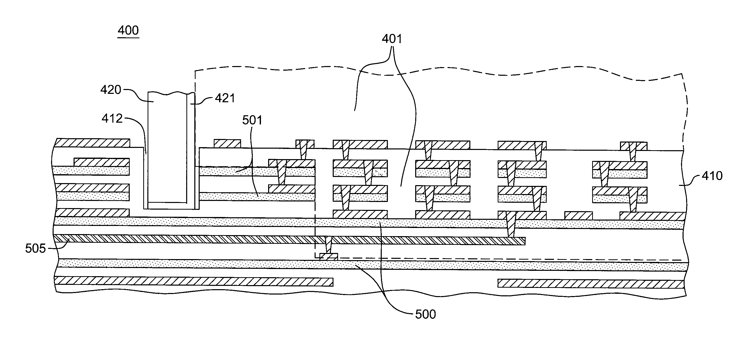
FIGS. 4A & 4B depict one embodiment of an electronic package, or tamper-proof electronic package 400, comprising an electronic circuit 415, in accordance with one or more aspects of the present invention.
Referring collectively to FIGS. 4A & 4B, electronic circuit 415 includes a multilayer circuit board 410 which has a tamper-respondent sensor 411 embedded therein that facilitates defining, in part, a secure volume 401 associated with multilayer circuit board 410 that extends into multilayer circuit board 410. In particular, in the embodiment of FIGS. 4A & 4B, secure volume 401 exists partially within multilayer circuit board 410, and partially above multilayer circuit board 410. One or more electronic components 402 are mounted to multilayer circuit board 410 within secure volume 401 and may comprise, for instance, one or more encryption modules and/or decryption modules, and associated components, with the tamper-proof electronic package comprising, in one or more embodiments, a communications card of a computer system.
Tamper-proof electronic package 400 further includes an enclosure 420, such as a pedestal-type enclosure, mounted to multilayer circuit board 410 within, for instance, a continuous groove (or trench) 412 formed within an upper surface of multilayer circuit board 410. In one or more embodiments, enclosure 420 may comprise a thermally conductive material and operate as a heat sink for facilitating cooling of the one or more electronic components 402 within the secure volume. A security mesh 421, such as the above-described security meshes, may be associated with enclosure 420, for example, wrapping around the inner surface of enclosure 420 to facilitate defining, in combination with tamper-respondent sensor 411 embedded within multilayer circuit board 410, secure volume 401. In one or more implementations, security mesh 421 extends down into continuous groove 412 in multilayer circuit board 410 and may, for instance, even wrap partially or fully around the lower edge of enclosure 420 within continuous groove 412 to provide enhanced tamper detection where enclosure 420 couples to multilayer circuit board 410. In one or more implementations, enclosure 420 may be securely affixed to multilayer circuit board 410 using, for instance, a bonding material such as an epoxy or other adhesive.
As depicted in FIG. 4B, one or more external circuit connection vias 413 may be provided within multilayer circuit board 410 for electrically connecting to the one or more electronic components 402 (FIG. 4A) within secure volume 401. These one or more external circuit connection vias 413 may electrically connect to one or more external signal lines or planes (not shown) embedded within multilayer circuit board 410 and extending, for instance, into a secure base region of (or below) secure volume 401, as explained further below. Electrical connections to and from secure volume 401 may be provided by coupling to such external signal lines or planes within the multilayer circuit board 410.
As noted with reference to FIGS. 4A & 4B, secure volume 401 defined in association with multilayer circuit board 410 may be sized to house electronic components 402 to be protected, and be constructed to extend into multilayer circuit board 410. In one or more implementations, multilayer circuit board 410 includes electrical interconnect within the secure volume 401 defined in the board, for instance, for electrically connecting the multiple tamper-respondent layers of the embedded tamper-respondent sensor 411 to associated monitor circuitry also disposed within secure volume 401.
Note that the embodiment depicted in FIGS. 4A & 4B is presented by way of example only. In one or more other implementations, the electronic circuit may comprise multiple multilayer circuit boards, each with a tamper-respondent sensor embedded within the multilayer circuit board with an appropriate connector, located within a secure volume defined between two adjacent multilayer circuit boards, interconnecting selected wiring of the multilayer circuit boards. In such an implementation, the overlying multilayer circuit board could be hollowed out to accommodate, for instance, the connector and/or one or more other electronic components between the multilayer circuit boards. In addition, other configurations of enclosure 420, and/or other approaches to coupling enclosure 420 and multilayer circuit board 410 may be employed.
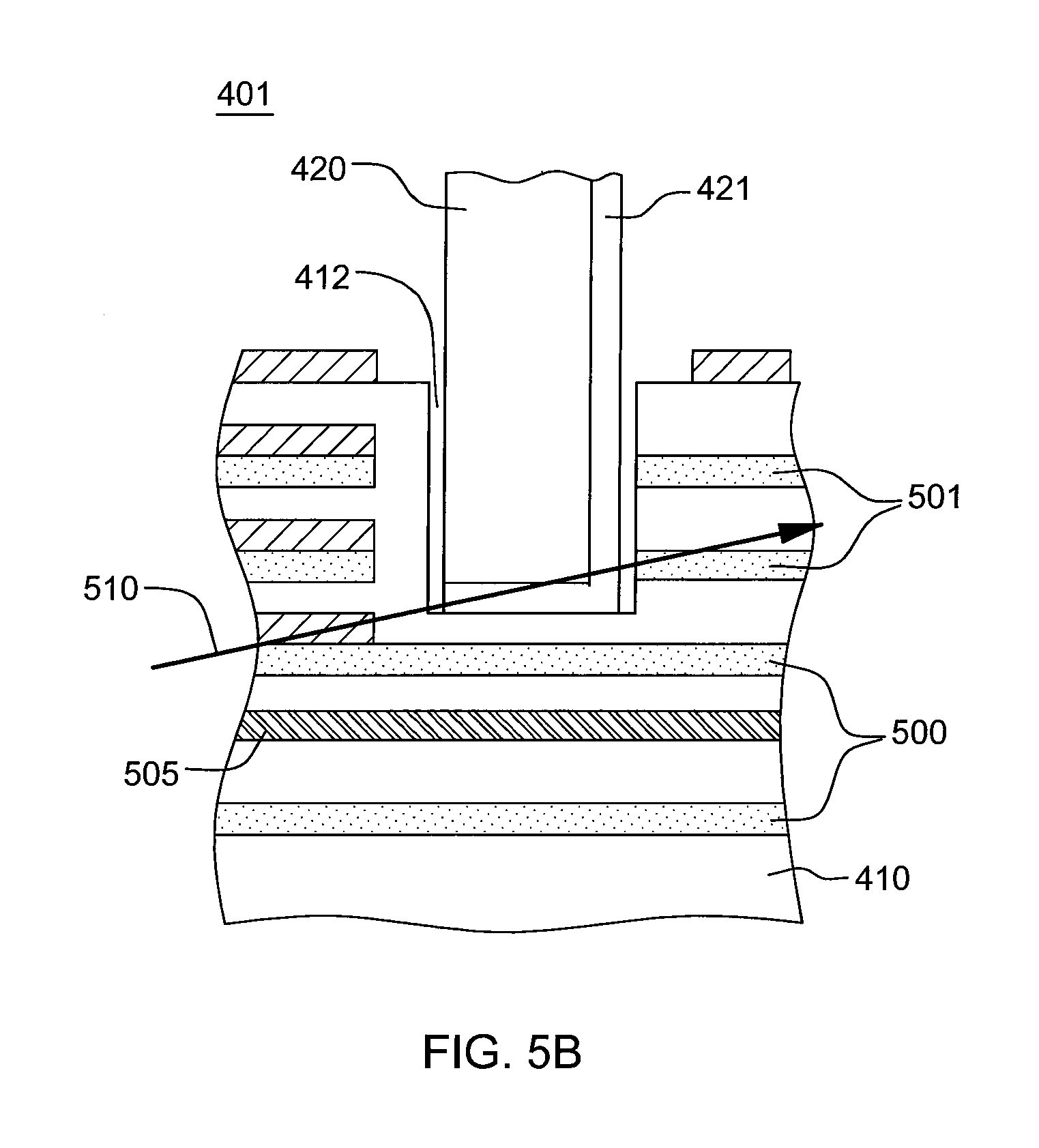
By way of further example, FIG. 5A depicts a partial cross-sectional elevational view of one embodiment of multilayer circuit board 410 and enclosure 420. In this configuration, the embedded tamper-respondent sensor includes multiple tamper-respondent layers including, by way of example, at least one tamper-respondent mat (or base) layer 500, and at least one tamper-respondent frame 501. In the example depicted, two tamper-respondent mat layers 500 and two tamper-respondent frame 501 are illustrated, by way of example only. The lower-most tamper-respondent mat layer 500 may be a continuous sense or detect layer extending completely below the secure volume being defined within multilayer circuit board 410. One or both tamper-respondent mat layers 500 below secure volume 401 may be partitioned into multiple circuit zones, as discussed further below. Within each tamper-respondent mat layer, or more particularly, within each circuit zone of each tamper-respondent mat layer, multiple circuits or conductive traces are provided in any desired configuration, such as the configuration described above in connection with FIG. 3. Further, the conductive traces within the tamper-respondent layers may be implemented as, for instance, a resistive layer which is difficult to attach shunt circuits to, as explained further below.
As illustrated, one or more external signal lines or planes 505 enter secure volume 401 between, in this embodiment, two tamper-respondent mat layers 500, and then electrically connect upwards into the secure volume 401 through one or more conductive vias, arranged in any desired location and pattern. In the configuration depicted, the one or more tamper-respondent frames 501 are disposed at least inside of the area defined by continuous groove 412 accommodating the base of enclosure 420. Together with security mesh 421 associated with enclosure 420, tamper-respondent frames 501 define secure volume 401 where extending, in part, into multilayer circuit board 410. With secure volume 401 defined, at least in part, within multilayer circuit board 410, the external signal line(s) 505 may be securely electrically connected to, for instance, the one or more electronic components 402 (FIG. 4A) mounted to multilayer circuit board 410 within secure volume 401. In addition, the secure volume 401 may accommodate electrical interconnection of the conductive traces of the multiple tamper-respondent layers, for instance, via appropriate monitor circuitry.
As illustrated by the schematic of FIG. 5B, added security may be provided by extending tamper-respondent mat layers 500 (and if desired, tamper-respondent frames 501) outward past continuous groove 412 accommodating enclosure 420. In this manner, a line of attack 510 may be made more difficult at the interface between enclosure 420 and multilayer circuit board 410 since the attack 510 would need to clear tamper-respondent mat layers 500, the bottom edge of security mesh 421 associated with enclosure 420, as well as the tamper-respondent frames 501 of the embedded tamper-respondent sensor.
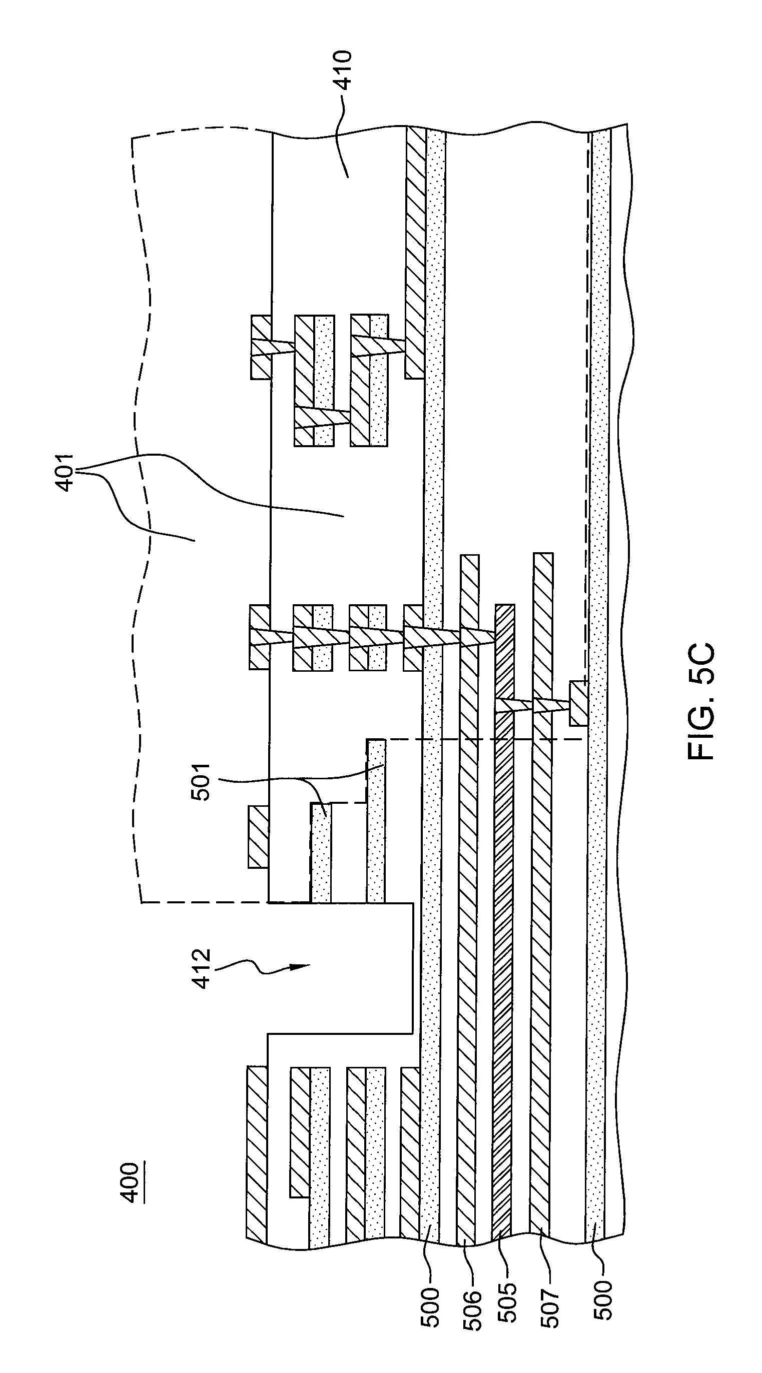
FIG. 5C depicts a variation on the multilayer circuit board 410 of FIG. 5A. In this embodiment, the embedded tamper-respondent sensor again includes multiple tamper-respondent mat layers 500 and multiple tamper-respondent frames 501, such as described above. Additionally, a tri-plate structure is provided comprising one or more external signal lines or layers 505 sandwiched between an upper ground plane 506 and a lower ground plane 507. In this configuration, high-speed transfer of signals to and from the secure volume, and in particular, to and from the one or more electronic components resident within the secure volume, are facilitated.
Note also that, in this implementation, once within the secure volume is defined within multilayer circuit board 410, conductive vias within the secure volume between layers of multilayer circuit board 410 may be either aligned, or offset, as desired, dependent upon the implementation. Alignment of conductive vias may facilitate, for instance, providing a shortest connection path, while offsetting conductive vias between layers may further enhance security of the tamper-proof electronic package by making an attack into the secure volume through or around one or more tamper-respondent layers of the multiple tamper-respondent layers more difficult.
Each tamper-respondent layer of the embedded tamper-respondent sensor formed within the multilayer circuit board of the electronic circuit or electronic package may include multiple conductive traces or lines formed between, for instance, respective sets of input and output contacts or vias at the trace termination points. Any number of conductive traces or circuits may be employed in defining a tamper-respondent layer or a tamper-respondent circuit zone within a tamper-respondent layer. For instance, 4, 6, 8, etc., conductive traces may be formed in parallel (or otherwise) within a given tamper-respondent layer or circuit zone between the respective sets of input and output contacts to those conductive traces.
In one or more implementations, the multilayer circuit board may be a multilayer wiring board or printed circuit board formed, for instance, by building up the multiple layers of the board. FIG. 6 illustrates one embodiment for forming and patterning a tamper-respondent layer within such a multilayer circuit board.
As illustrated in FIG. 6, in one or more implementations, a tamper-respondent layer, such as a tamper-respondent mat layer or a tamper-respondent frame disclosed herein, may be formed by providing a material stack comprising, at least in part, a structural layer 601, such as a pre-preg (or pre-impregnated) material layer, a trace material layer 602 for use in defining the desired trace patterns, and an overlying conductive material layer 603, to be patterned to define conductive contacts or vias electrically connecting to the pattern of traces being formed within the trace material layer 602, for instance, at trace terminal points. In one or more implementations, the trace material layer 602 may comprise nickel phosphorous (NiP), and the overlying conductive layer 603 may comprise copper. Note that these materials are identified by way of example only, and that other trace and/or conductive materials may be used within the build-up layer or stack 600.
A first photoresist 604 is provided over stack 600, and patterned with one or more openings 605, through which the overlying conductive layer 603 may be etched. Depending on the materials employed, and the etch processes used, a second etch process may be desired to remove portions of trace material layer 602 to define the conductive traces of the subject tamper-respondent layer. First photoresist 604 may then be removed, and a second photoresist 604' is provided over the conductive layer 603 features to remain, such as the input and output contacts. Exposed portions of conductive layer 603 are then etched, and the second photoresist 604' may be removed, with any opening in the layer being filled, for instance, with an adhesive (or pre-preg) and a next build-up layer is provided, as shown. Note that in this implementation, most of overlying conductive layer 603 is etched away, with only the conductive contacts or vias remaining where desired, for instance, at the terminal points of the traces formed within the layer by the patterning of the trace material layer 602. Note that any of a variety of materials may be employed to form the conductive lines or traces within a tamper-respondent layer. Nickel-phosphorous (NiP) is particularly advantageous as a material since it is resistant to contact by solder, or use of a conductive adhesive to bond to it, making it harder to bridge from one circuit or trace to the next during an attempt to penetrate into the protected secure volume of the electronic circuit. Other materials which could be employed include OhmegaPly.RTM., offered by Ohmega Technologies, Inc., of Culver City, Calif. (USA), or Ticer.TM., offered by Ticer Technologies of Chandler, Ariz. (USA).
By way of example, FIG. 7 is a partial plan view of one embodiment of a tamper-respondent mat layer 500 of an embedded tamper-respondent sensor within a multilayer circuit board, in accordance with one or more aspects of the present invention. In this implementation, tamper-respondent mat layer 500 is divided into multiple tamper-respondent circuit zones 701, 702, 703, 704, 705, of varying sizes. Within each tamper-respondent circuit zone 701, 702, 703, 704, 705, conductive traces of the same or different wiring patterns may be provided with, for instance, the larger circuit zones 701, 703, 705, having a same number of traces and similar resistance per trace, per zone. Note that other configurations of tamper-respondent sense zones may be employed, including, for instance, equal or standard-sized circuit zones within a common tamper-respondent layer.
FIGS. 8A-8G depict, by way of example, one embodiment of multiple tamper-respondent layers, and the electrical interconnect associated with the tamper-respondent layers, such as for, for instance, the embedded tamper-respondent sensor depicted in FIG. 5A.
As illustrated in FIG. 8A, blind contact vias 710, 711 are provided, by way of example, at the edge or boundary of each tamper-respondent circuit zone 701, 702, 703, 704, 705 within a lowermost tamper-respondent mat layer 500. Contact vias 710, 711 facilitate electrical connection from the ends of the conductive traces (not shown) of the depicted tamper-respondent layer upwards into the secure volume for connection to appropriate monitor circuitry in any desired configuration. Note with respect to FIG. 8A, that there are no penetrations through the lowermost tamper-respondent mat layer 500. As explained further below, in one or more implementations, electrical interconnect may be provided above the lowermost tamper-respondent mat layer to shift the overlying contact vias to, for instance, the centers of tamper-respondent circuit zones 702, 704, for instance, to prevent direct penetration of one tamper-respondent layer from passing through other tamper-respondent layers. As noted, any desired number and size of circuit zones of traces may be defined within a tamper-respondent layer. In one or more implementations, a tamper-respondent mat layer may include, for instance, 20, 30, 40, or more, tamper-respondent circuit zones within the layer, each with a same number of traces.
FIG. 8B is a partial enlarged depiction of tamper-respondent mat layer 500 of FIG. 8A, showing a partial boundary between two tamper-respondent circuit zones 701, 702, with input contacts or vias 710 depicted. In this example, an 8-band trace pattern of conductive traces or lines 800 is partially shown within circuit zones 701, 702. As noted, the pattern of conductive traces 800 may be provided in any desired configuration and include, for instance, saw-tooth or sinusoidal line portions within the respective circuit zones 701, 702. FIG. 8B depicts an example of the start of a pattern of the conductive traces 800 where connected to input contacts or vias 710. Configuring conductive traces 800 as illustrated further enhances security by making it harder to reach multiple vias to jump over or shut sections of circuitry within a particular tamper-respondent layer of the embedded tamper-respondent sensor. In one or more implementations the trace fill pattern is dense. Further, line-to-line or trace-to-trace spacing between the different circuit zones of a particular tamper-respondent layer may be the same as that employed within a particular tamper-respondent circuit zone.
FIG. 8C depicts an electrical interconnect layer over tamper-respondent mat layer 500 of FIG. 8A, with wiring illustrated to shift the conductive contacts to offset the vias to, by way of example, the middle of tamper-respondent circuit zones 702, 704. Additionally, this interconnect layer may comprise the external signal lines and contacts for connecting to and from the secure volume to external the secure volume, including, if desired, the provision of one or more high-speed interconnect circuits sandwiched between, for instance, respective ground planes, such as noted above with reference to the exemplary embodiment of FIG. 5C. As illustrated, conductive lines 811 may be provided in this layer electrically connecting contacts 710, 711 of the respective tamper-respondent circuit zones to offset vias 812, 813 disposed, for instance, in alignment 810 over tamper-respondent circuit zones 702, 704. In addition, one or more external signal line contacts 815 may also be provided in this electrical interconnect layer for facilitating electrical connection of the external signal lines into the secure volume.
FIG. 8D depicts a second tamper-respondent mat layer 500, which in this example, is disposed above tamper-respondent mat layer 500 discussed above in connection with FIGS. 8A & 8B. This second tamper-respondent mat layer 500 is similar to the first except, in the depicted embodiment, the sizes of the tamper-respondent circuit zones 721, 722, 723, 724, 725, are different from the tamper-respondent circuit zones 701, 702, 703, 704, 705, of the tamper-respondent mat layer 500 of FIGS. 8A & 8B. Thus, the boundaries between the tamper-respondent circuit zones between the different layers are offset. This advantageously reduces the opportunity to penetrate both tamper-respondent mat layers along a zone boundary or seam. Depending upon the implementation, electrical contacts to the depicted circuit vias or contacts in the tamper-respondent circuit zones depicted may extend directly upwards into the secure volume. Alternatively, contact vias may be further offset into, for instance, the center lines of tamper-respondent circuit zones 722, 724, in a manner similar to that described above in connection with FIG. 8C. As described above, within each tamper-respondent circuit zone 721-725, a pattern of conductive traces (not shown) is provided. In one or more implementations, tamper-respondent mat layer 500 depicted in FIG. 8D may again comprise any desired number of circuit zones, such as 20, 30, 40, or more, circuit zones, each of which electrically connects within the secure volume in any desired monitor circuitry configuration. Note also that, in one or more embodiments, contacts or vias from the signal layer(s) and/or the lowermost tamper-respondent may layer, may extend through this second tamper-respondent mat layer.
FIG. 8E depicts an exemplary embodiment of a tamper-respondent frame 501 of a tamper-respondent sensor, in accordance with one or more aspects of the present invention. Tamper-respondent frame 501 resides over the tamper-respondent mat layers 500 described above in connection with FIGS. 8A-8D, and is in one or more embodiments, a picture frame-type layer which completely encircles, and thus serves to define, the secure volume 401 (FIGS. 4A & 5A) within the multilayer circuit board. The tamper-respondent frame illustrated may be a first tamper-respondent frame 501, which provides protective sense wiring or traces, either on the inside or the outside of the enclosure 420 (see FIGS. 4A & 5A), where coupled to the continuous groove or trench within the multilayer circuit board.
FIG. 8F depicts an exemplary embodiment of conductive contacts or vias 710, 711 for tamper-respondent frame 501 of FIG. 8E, with four trace lines being depicted, by way of example only. As illustrated, the input contacts 710 and output contacts 711 at the trace terminal points in a particular zone may be disposed in close proximity with the trace lines 801 of tamper-respondent frame 501, and overlap or double back at the seam to minimize possibility of a successful attack through tamper-respondent frame 501 at the seam.
FIG. 8G depicts a second tamper-respondent frame 501, which in one or more embodiments, overlies the first tamper-respondent frame 501 of FIG. 8E (in the example of FIG. 5A), and which may be identical to the first tamper-respondent frame, except rotated 180.degree. so that the wiring contacts 710, 711 are separated from the layer below, as illustrated. As with the tamper-respondent mat layers 500, tamper-respondent frames 501 may be divided into distinct circuit zones to, for instance, further enhance security. For instance, 2, 4, 6, or more, circuit zones may be defined within a particular tamper-respondent frame 501, each with a plurality of conductive traces defined between input contacts 710 and output contacts 711 at the trace terminal points.
The trace lines or circuits within all of the tamper-respondent layers, and in particular, the tamper-respondent circuit zones, of the embedded tamper-respondent sensor are electrically connected into monitor or compare circuitry 900 provided, for instance, within secure volume 401 of multilayer circuit board 410, as illustrated in FIG. 9. Monitor circuitry 900 may include various bridge or compare circuits, and conventional printed wiring board electrical interconnect inside the secure volume 401, for instance, located within the secure volume defined by the tamper-respondent frames 501 (FIG. 5A), and the tamper-respondent mat layers.
Note that advantageously, different tamper-respondent circuit zones on different tamper-respondent layers may be electrically interconnected into, for instance, the same comparator circuit or Wheatstone bridge of the monitor circuitry. Thus, any of a large number of interconnect configurations may be possible. For instance, if each tamper-respondent mat layer contains 30 tamper-respondent circuit zones, and each tamper-respondent frame contains four tamper-respondent circuit zones, then, for instance, the resultant sixty-eight tamper-respondent circuit zones may be connected in any configuration within the secure volume to create the desired arrangement of circuit networks within the secure volume being monitored for changes in resistance or tampering. Note in this regard, that the power supply or battery for the tamper-respondent sensor may be located external to the secure volume, with the sensor being configured to trip and destroy any protected or critical data if the power supply or battery is tampered with.
The terminology used herein is for the purpose of describing particular embodiments only and is not intended to be limiting of the invention. As used herein, the singular forms "a", "an" and "the" are intended to include the plural forms as well, unless the context clearly indicates otherwise. It will be further understood that the terms "comprise" (and any form of comprise, such as "comprises" and "comprising"), "have" (and any form of have, such as "has" and "having"), "include" (and any form of include, such as "includes" and "including"), and "contain" (and any form contain, such as "contains" and "containing") are open-ended linking verbs. As a result, a method or device that "comprises", "has", "includes" or "contains" one or more steps or elements possesses those one or more steps or elements, but is not limited to possessing only those one or more steps or elements. Likewise, a step of a method or an element of a device that "comprises", "has", "includes" or "contains" one or more features possesses those one or more features, but is not limited to possessing only those one or more features. Furthermore, a device or structure that is configured in a certain way is configured in at least that way, but may also be configured in ways that are not listed.
The corresponding structures, materials, acts, and equivalents of all means or step plus function elements in the claims below, if any, are intended to include any structure, material, or act for performing the function in combination with other claimed elements as specifically claimed. The description of the present invention has been presented for purposes of illustration and description, but is not intended to be exhaustive or limited to the invention in the form disclosed. Many modifications and variations will be apparent to those of ordinary skill in the art without departing from the scope and spirit of the invention. The embodiment was chosen and described in order to best explain the principles of one or more aspects of the invention and the practical application, and to enable others of ordinary skill in the art to understand one or more aspects of the invention for various embodiments with various modifications as are suited to the particular use contemplated.
* * * * *
References
D00000
D00001
D00002
D00003
D00004
D00005
D00006
D00007
D00008
D00009
D00010
D00011
D00012
D00013

D00014

D00015

D00016

D00017

XML
uspto.report is an independent third-party trademark research tool that is not affiliated, endorsed, or sponsored by the United States Patent and Trademark Office (USPTO) or any other governmental organization. The information provided by uspto.report is based on publicly available data at the time of writing and is intended for informational purposes only.
While we strive to provide accurate and up-to-date information, we do not guarantee the accuracy, completeness, reliability, or suitability of the information displayed on this site. The use of this site is at your own risk. Any reliance you place on such information is therefore strictly at your own risk.
All official trademark data, including owner information, should be verified by visiting the official USPTO website at www.uspto.gov. This site is not intended to replace professional legal advice and should not be used as a substitute for consulting with a legal professional who is knowledgeable about trademark law.