Process for producing an intermetallic contact based on Ni on In.sub.xGa.sub.1-xAs
Rodriguez , et al.
U.S. patent number 10,361,087 [Application Number 16/024,008] was granted by the patent office on 2019-07-23 for process for producing an intermetallic contact based on ni on in.sub.xga.sub.1-xas. This patent grant is currently assigned to COMMISSARIAT A L'ENERGIE ATOMIQUE ET AUX ENERGIES ALTERNATIVES. The grantee listed for this patent is COMMISSARIAT A L'ENERGIE ATOMIQUE ET AUX ENERGIES ALTERNATIVES. Invention is credited to Patrice Gergaud, Fabrice Nemouchi, Philippe Rodriguez, Seifeddine Zhiou.


View All Diagrams
| United States Patent | 10,361,087 |
| Rodriguez , et al. | July 23, 2019 |
Process for producing an intermetallic contact based on Ni on In.sub.xGa.sub.1-xAs
Abstract
A process for manufacturing an intermetallic contact on the surface of a layer or of a substrate of oriented In.sub.xGa.sub.1-xAs material, the contact includes an Ni--InGaAs intermetallic compound, the intermetallic compound having a hexagonal crystallographic structure that may have: a first texture or a second texture formed at a second nucleation temperature above the first nucleation temperature; the process comprising the following steps: the production of nomograms defining, for a thickness of Ni deposited, the time to completely consume the initial thickness of Ni as a function of the annealing temperature, the annealing temperature being below the nucleation temperature of the second texture; the localized deposition of Ni on the surface of the In.sub.xGa.sub.1-xAs material; an annealing step applying the pair of parameters: time required/annealing temperature, deduced from the nomograms, comprising at least one temperature rise step and at least one temperature hold of the final annealing temperature.
| Inventors: | Rodriguez; Philippe (Le Grand-Lemps, FR), Zhiou; Seifeddine (Gafsa, TN), Nemouchi; Fabrice (Moirans, FR), Gergaud; Patrice (La Buisse, FR) | ||||||||||
|---|---|---|---|---|---|---|---|---|---|---|---|
| Applicant: |
|
||||||||||
| Assignee: | COMMISSARIAT A L'ENERGIE ATOMIQUE
ET AUX ENERGIES ALTERNATIVES (Paris, FR) |
||||||||||
| Family ID: | 60627697 | ||||||||||
| Appl. No.: | 16/024,008 | ||||||||||
| Filed: | June 29, 2018 |
Prior Publication Data
| Document Identifier | Publication Date | |
|---|---|---|
| US 20190006182 A1 | Jan 3, 2019 | |
Foreign Application Priority Data
| Jun 29, 2017 [FR] | 17 56022 | |||
| Current U.S. Class: | 1/1 |
| Current CPC Class: | H01L 21/28575 (20130101); H01L 29/41725 (20130101); H01L 21/283 (20130101); H01L 29/401 (20130101); H01L 29/452 (20130101) |
| Current International Class: | H01L 29/40 (20060101); H01L 29/45 (20060101); H01L 21/285 (20060101); H01L 29/417 (20060101); H01L 21/283 (20060101) |
| Field of Search: | ;257/295 |
References Cited [Referenced By]
U.S. Patent Documents
| 2011/0084320 | April 2011 | Jung |
| 2013/0052805 | February 2013 | Previtali |
Other References
|
Rabhi, et al., "Phase formation between Ni thin films and GaAs substrate", Scripta Materialia, vol. 141, pp. 28-31, Jul. 22, 2017. cited by applicant . Chuang, et al., "An Electrical Method to Characterize Thermal Reactions of Pd/GaAs and Ni/GaAs Contacts", Journal of Electronic Materials, vol. 24, No. 6, pp. 767-772, 1995. cited by applicant . Ghegin, et al., "Metallurgical Studies of Integrable Ni-based Contacts for Their Use in III-V/Si Heterogeneous Photonics Devices", Silicon Nanoelectronics Workshop (SNW), 2016. cited by applicant . Kim, et al., "Sub-60-nm Extremely Thin Body InxGa1--xAs-On-Insulator MOSFETs on Si With Ni--InGaAs Metal S/D and MOS Interface Buffer Engineering and Its Scalability", IEEE Transactions on Electron Devices, vol. 60, No. 8, pp. 2512-2517, Aug. 2013. cited by applicant . Shekhter, et al., "Epitaxial NiInGaAs Formed by Solid State Reaction on In0.53Ga0.47As: Structural and Chemical Study", Journal of Vacuum Science & Technology B, vol. 31, Issue 3, 2013. cited by applicant . Solomon, et al., "Auger Sputter Profiling and Factor Analysis of Thermally Treated Ni--GaAs Structures: The Influence of Oxygen on Compounding and Diffusion", Journal of Vacuum Science & Technology A 5, 1809 (1987). cited by applicant . Zhiou, et al., "Reaction of Ni film with In0.53Ga0.47As: Phase formation and texture", Journal of Applied Physics, American Institute of Physics, vol. 120, No. 13, Oct. 4, 2016, XP012212419. cited by applicant . Perrin, et al., "Formation of Ni3InGaAs phase in Ni/InGaAs contact at low temperature", Applied Physics Letters, A I P Publishing LLC, vol. 109, No. 13, Sep. 26, 2016, XP012212253. cited by applicant . Ivana, et al., "Crystal structure and epitaxial relationship of NiInGaAs films formed on InGaAs by annealing", Journal of Vacuum Science & Technology B: Microelectronics and Nanometer Structures, American Institute of Physics, vol. 31, No. 1, Jan. 1, 2013, pp. 12202-1-12202-8, XP012172447. cited by applicant . Ashizawa, et al., "Thermal stability of interfaces between metals and InP-based materials", Journal of Electronic aterials, vol. 25, No. 4. pp. 715-519, 1996. cited by applicant. |
Primary Examiner: Luu; Chuong A
Attorney, Agent or Firm: Baker & Hostetler LLP
Claims
The invention claimed is:
1. A process for manufacturing an intermetallic contact on the surface of a layer or of a substrate of oriented In.sub.xGa.sub.1-xAs material with 0.ltoreq.x.ltoreq.1, said contact comprising an Ni--InGaAs intermetallic compound, said intermetallic compound having a hexagonal crystallographic structure that may have: a first texture, of which (1010) planes of the intermetallic compound are parallel to the surface of said layer or of said substrate, and which is formed at a first nucleation temperature or a second texture, of which the (0001) planes of the intermetallic compound are parallel to the planes of said layer or of said substrate, and which is formed at a second nucleation temperature above said first nucleation temperature; said process comprising the following steps: the production of nomograms defining, for a thickness of Ni deposited on said In.sub.xGa.sub.1-xAs material, the time required to completely consume the initial thickness of Ni deposited on said In.sub.xGa.sub.1-xAs material as a function of the annealing temperature, said annealing temperature being below said nucleation temperature of said second texture; the localized deposition of Ni on the surface of said In.sub.xGa.sub.1-xAs material in order to form a layer of Ni having a contact thickness; an annealing step applying the pair of parameters: time required/annealing temperature, deduced from said nomograms in correlation with said contact thickness so as to form, by solid-state reaction, a layer of intermetallic compound of first texture, said annealing step comprising: at least one temperature rise step with a given temperature rise rate that makes it possible to achieve a final annealing temperature (T.sub.p) and at least one temperature hold of said final annealing temperature (T.sub.p), for a hold time (.DELTA.t.sub.p).
2. The process for manufacturing an intermetallic contact according to claim 1, wherein the temperature rise rate is determined as being below a maximum rate V.sub.max (in .degree. C./min), said maximum rate being defined by the following function as a function of the thickness x (in nm) of Ni deposited: V.sub.max=12314.7x.sup.-1.91582
3. The process for manufacturing an intermetallic contact according to claim 1, wherein said annealing step comprises: a first temperature rise step with a first temperature rise rate that makes it possible to achieve a first annealing temperature (T.sub.1r); a second temperature rise step with a second temperature rise rate that makes it possible to achieve, from said first annealing temperature, a final annealing temperature (T.sub.p); at least one temperature hold of said final annealing temperature (T.sub.p), for a hold time (.DELTA.t.sub.p).
4. The process for manufacturing an intermetallic contact according to claim 1, wherein the molar fraction x of the substrate is between 0.25 and 0.80.
5. The process for manufacturing an intermetallic contact according to claim 1, comprising a first annealing at a first temperature for a first time in order to form a first intermetallic compound of first texture and having a first phase and a second annealing at a higher temperature than said first temperature in order to form a second intermetallic compound of first texture and having a second phase.
6. The process for manufacturing an intermetallic contact according to claim 1, comprising an annealing carried out at a temperature between 200.degree. C. and 320.degree. C., with a preference for the range 240.degree. C. and 290.degree. C., for a time dependent on the thickness of Ni deposited, in order to form an Ni.sub.3InGaAs intermetallic compound.
7. The process for manufacturing an intermetallic contact according to claim 6, wherein, the initial thickness of Ni being between a few nanometers and a few tens of nanometers, the annealing time varies between a few minutes and a few tens of minutes.
8. The process for manufacturing according to claim 6, wherein said annealing carried out at a temperature between 200.degree. C. and 320.degree. C., with a preference for the range 240.degree. C. and 290.degree. C., is followed by an annealing carried out at a temperature between 250.degree. C. and 550.degree. C. in order to modify the resistivity of said intermetallic contact formed.
9. The process according to claim 7, wherein said annealing carried out at a temperature between 200.degree. C. and 320.degree. C., with a preference for the range 240.degree. C. and 290.degree. C., is followed by an annealing carried out at a temperature between 250.degree. C. and 350.degree. C. in order to form an Ni.sub.3InGaAs compound.
10. The process for manufacturing an intermetallic contact according to claim 1, wherein the nomograms are produced by measuring the intermetallic compound thicknesses formed as a function of time.
11. The process for manufacturing an intermetallic contact according to claim 10, wherein the thickness measurements are performed by x-rays.
12. The process for manufacturing an intermetallic contact according to claim 10, wherein the thickness measurements are performed by ellipsometry.
13. The process for manufacturing an intermetallic contact according to claim 1, comprising the deposition of a protective layer on the surface of the localized deposition of Ni, prior to the annealing operation(s).
14. An intermetallic contact obtained according to the process of claim 1.
15. A process for manufacturing a transistor comprising the process for manufacturing an intermetallic contact according to claim 1.
16. A process for manufacturing a photonic component comprising the process for manufacturing an intermetallic contact according to claim 1.
Description
CROSS-REFERENCE TO RELATED APPLICATIONS
This application claims priority to foreign French patent application No. FR 1756022, filed on Jun. 29, 2017, the disclosure of which is incorporated by reference in its entirety.
FIELD OF THE INVENTION
The field of the invention is that of components made of III-V materials and more precisely that of In.sub.xGa.sub.1-xAs components with 0.ltoreq.x.ltoreq.1, comprising the production of intermetallic contacts.
BACKGROUND
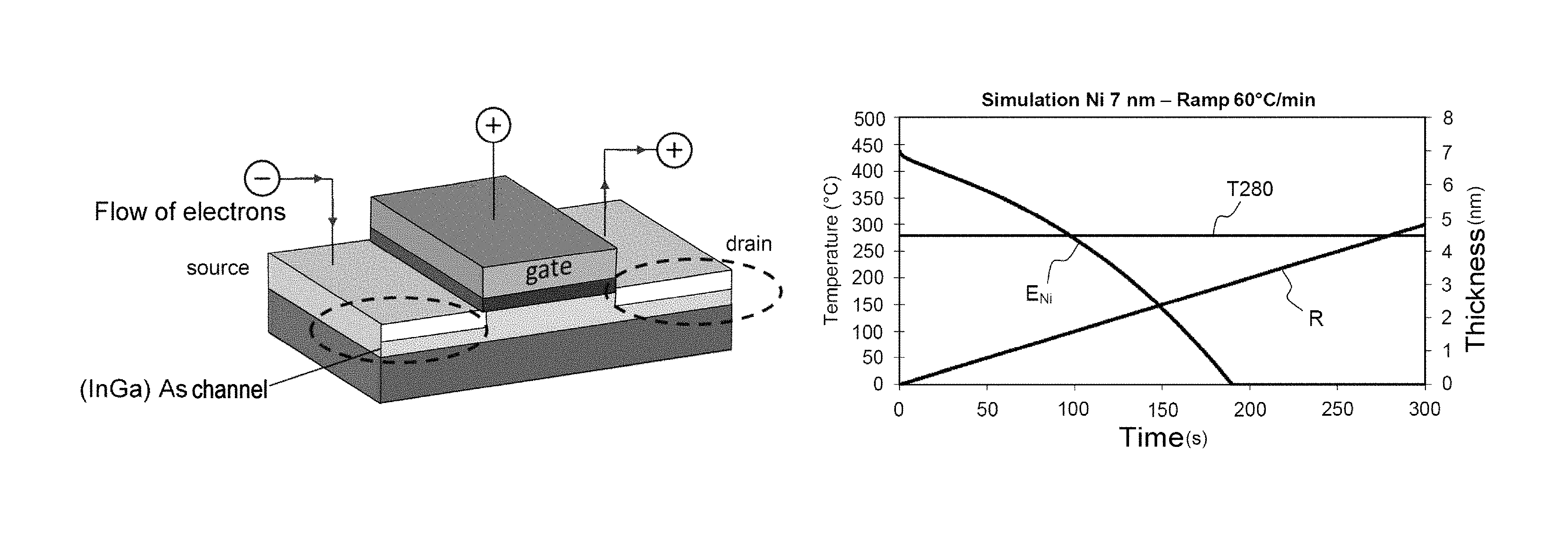
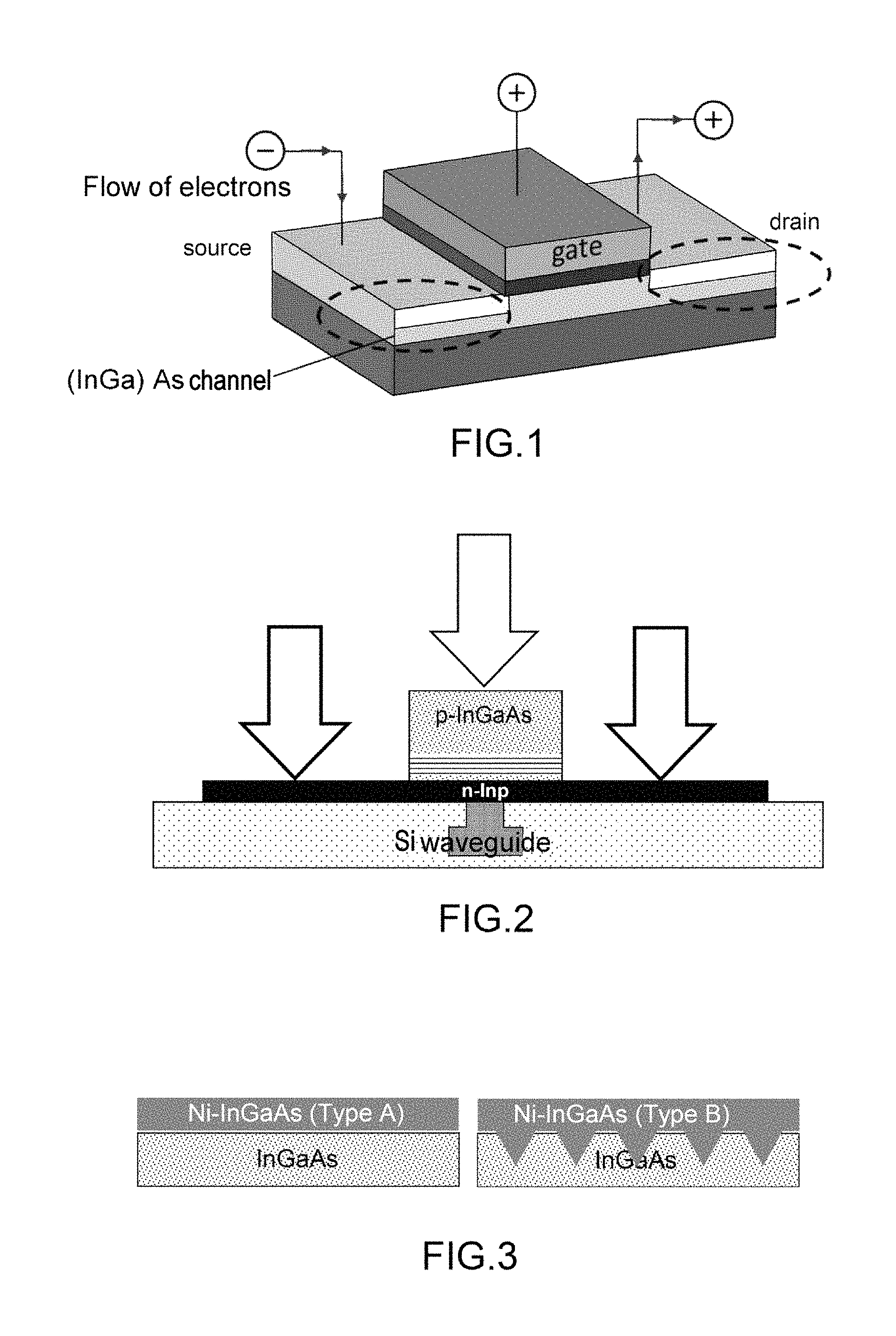
FIG. 1 thus illustrates an example of a transistor comprising an In.sub.xGa.sub.1-xAs channel highlighting the source, the gate and the drain, requiring the making of contacts. FIG. 2 illustrates another type of configuration for photonic applications that also requires the making of contacts and in which the present invention may be particularly of interest.
Contacts on In.sub.xGa.sub.1-xAs with 0.ltoreq.x.ltoreq.1 that are compatible with a Si-CMOS technology are generally produced by solid-state reaction between a metal (Ni) or a metal alloy Ni.sub.yM.sub.1-y and the semiconductor (InGaAs) as described in the publication by S. H. Kim et al., IEDM 2010, 26.6.
This reaction, carried out between 200.degree. C. and 500.degree. C. by rapid annealing in a controlled atmosphere results in an Ni--InGaAs intermetallic compound being obtained, as described in the publication by Ivana et al., J. Vac. Sci. Technol., B 31 (2013) 012202 and in the publication by P. Shekter et al., J. Vac. Sci. Technol., B 31 (2013) 031205, which can be used for the making of S/D contacts of the transistor as described in the publication by S. H. Kim et al., IEEE Trans. Electron. Devices 60 (2013) 2512 or to contact the electrode used for electrical pumping of the laser as described in the publication by E. Ghegin et al., IEEE Silicon Nanoelectronics Workshop 2016, 214.
To date, the nature of the phases and of the textures obtained during the solid-state reaction between Ni and InGaAs was not properly known as described in the publication by S. Zhiou et al., J. Appl. Phys. 120 (2016) 13530.
Yet control of the latter may result in an optimized intermetallic compound being obtained, which inter metallic compound is optimized in particular in terms of morphological stability, thickness and contact resistivity enabling a control of the production of the contacts.
This is why in this context the present invention relates to a process for manufacturing an optimized intermetallic contact.
The Applicant proposes a process that makes it possible to control the phases and the textures of the Ni--InGaAs intermetallic compound, based on an in-depth study of the solid-state reaction between the Ni metal and the In.sub.xGa.sub.1-xAs compound with 0.ltoreq.x.ltoreq.1, this being in order to favor: a texture that results in an optimized contact interface and an optimized morphology; a hexagonal phase with well-defined stoichiometry which is favorable in terms of contact resistivity.
SUMMARY OF THE INVENTION
The advantage of the present invention lies in the fact of carrying out a process for obtaining an intermetallic compound that makes it possible to remain below the nucleation barrier of the unfavorable texture while not all the Ni has been consumed.
Compared to the prior art, the present invention provides a solution that makes it possible to reproducibly control the morphology of the contacts through control of the texture and of the phase and therefore to favor a lower resistivity.
The present invention relates to a process that, by a thermal annealing operation calibrated as a function of the thickness of nickel deposited, makes it possible to only form one type of desired first texture while avoiding forming an undesirable second texture as will be explained and expanded upon in the detailed description of the present application.
More specifically, one subject of the invention is a process for manufacturing an intermetallic contact on the surface of a layer or of a substrate of (100) oriented In.sub.xGa.sub.1-xAs material with 0.ltoreq.x.ltoreq.1, said contact comprising an Ni--InGaAs intermetallic compound, said intermetallic compound having a hexagonal crystallographic structure that may have:
a first texture, of which (1010) planes of the intermetallic compound are parallel to the surface of said layer or of said substrate, and which is formed at a first nucleation temperature or
a second texture, of which the (0001) planes of the intermetallic compound are parallel to the (111) planes of said layer or of said substrate, and which is formed at a second nucleation temperature above said first nucleation temperature;
said process comprising the following steps:
the production of nomograms defining, for a thickness of Ni deposited on said In.sub.xGa.sub.1-xAs material, the time required to completely consume the initial thickness of Ni deposited on said In.sub.xGa.sub.1-xAs material as a function of the annealing temperature, said annealing temperature being below said nucleation temperature of said second texture;
the localized deposition of Ni on the surface of said In.sub.xGa.sub.1-xAs material in order to form a layer of Ni having a contact thickness;
an annealing step applying the pair of parameters: time required/annealing temperature, deduced from said nomograms in correlation with said contact thickness so as to form, by solid-state reaction, a layer of intermetallic compound of first texture, said annealing step comprising:
at least one temperature rise step with a given temperature rise rate that makes it possible to achieve a final annealing temperature T.sub.p and
at least one temperature hold of said final annealing temperature T.sub.p, for a hold time .DELTA.t.sub.p.
Advantageously, the temperature rise rate is determined as being below a maximum rate V.sub.max, said maximum rate depending on the kinetics of the texture that is formed.
Advantageously, the maximum annealing rate (in .degree. C./min) corresponds to the following equation as a function of the thickness of Ni deposited (in nm): V.sub.max=12314.7x.sup.-1.91582
Advantageously, the process of the invention may comprise, regarding the annealing step:
a first temperature rise step with a first temperature rise rate that makes it possible to achieve a first annealing temperature T.sub.1r;
a second temperature rise step with a second temperature rise rate that makes it possible to achieve, from said first annealing temperature, a final annealing temperature T.sub.p;
at least one temperature hold of said final annealing temperature T.sub.p, for a hold time .DELTA.t.sub.p.
Advantageously, the molar fraction x of the substrate is between 0.25 and 0.80.
According to variants of the invention, the process comprises a first annealing at a first temperature for a first time in order to form a first intermetallic compound of first texture and having a first phase and a second annealing at a higher temperature than said first temperature in order to form a second intermetallic compound of first texture and having a second phase.
The Ni--InGaAs intermetallic compound may typically be an Ni.sub.2InGaAs compound or an Ni.sub.3InGaAs compound.
According to variants of the invention, the process comprises an annealing carried out at a temperature between 200.degree. C. and 320.degree. C., in order to form the first texture A, with a preference for the range 240.degree. C. and 290.degree. C., for a time dependent on the thickness of Ni deposited, in order to form an Ni.sub.3InGaAs intermetallic compound.
Typically, for an initial thickness of Ni of between a few nanometers and a few tens of nanometers, the annealing time may vary between a few minutes and a few tens of minutes.
According to variants of the invention, said annealing carried out at a temperature between 200.degree. C. and 320.degree. C., with a preference for the range 240.degree. C. and 290.degree. C., is followed by an annealing carried out at a temperature between 250.degree. C. and 550.degree. C. in order to modify the resistivity of said intermetallic contact formed.
According to variants of the invention, said annealing carried out at a temperature between 200.degree. C. and 320.degree. C., with a preference for the range 240.degree. C. and 290.degree. C., is followed by an annealing carried out at a temperature between 300.degree. C. and 500.degree. C. in order to consolidate the Ni.sub.zInGaAs phase (in the low range) or to form the Ni.sub.2InGaAs phase (in the high range).
It should be noted that the two Ni.sub.3InGaAs and Ni.sub.2InGaAs phases have the same structure with variable compositions depending on the degree of occupation of the interstitial sites, the Ni.sub.2InGaAs phase being the most stable phase at high temperature (350-500.degree. C.).
According to variants of the invention, the nomograms are produced by measuring the intermetallic compound thicknesses formed as a function of time.
According to variants of the invention, the thickness measurements are performed by x-ray reflectivity.
According to variants of the invention, the thickness measurements are performed by ellipsometry.
According to variants of the invention, the process comprises the deposition of a protective layer on the surface of the localized deposition of Ni, prior to the annealing operation(s).
Another subject of the invention is the intermetallic contact obtained according to the process of the invention.
A further subject of the invention is a process for manufacturing a transistor comprising the process for manufacturing an intermetallic contact of the invention.
Another subject of the invention is a process for manufacturing a photonic component comprising the process for manufacturing an intermetallic contact of the invention.
BRIEF DESCRIPTION OF THE DRAWINGS
A better understanding of the invention will be obtained and other advantages will become apparent on reading the description which will follow, given without limitation, and by virtue of the figures, among which:
FIG. 1 illustrates an example of a transistor structure according to the known art that may comprise intermetallic contacts;
FIG. 2 illustrates an example of a photonic structure according to the known art that may comprise intermetallic contacts;
FIG. 3 depicts the two textures of the Ni--InGaAs intermetallic compound that may be obtained during an annealing operation;
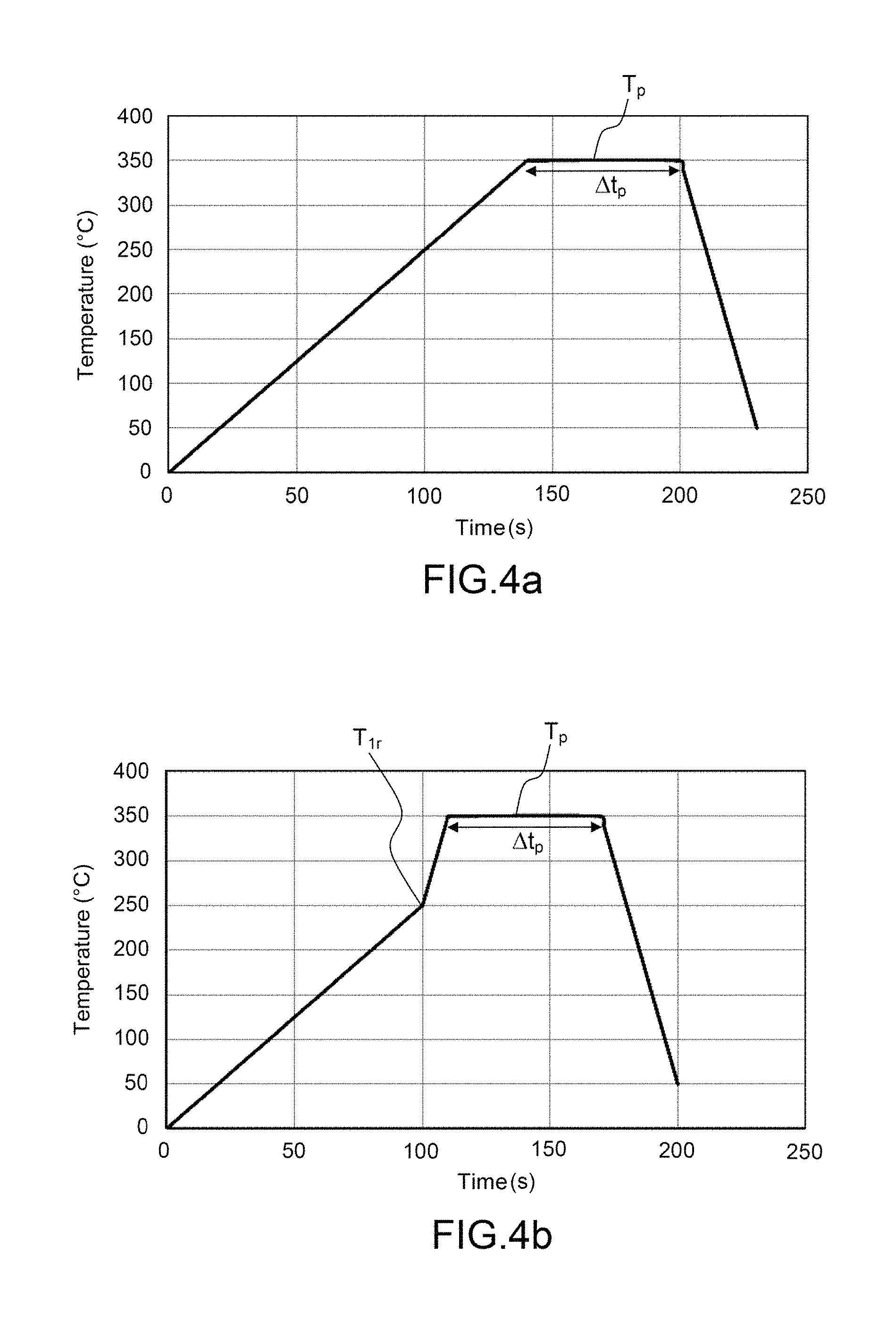
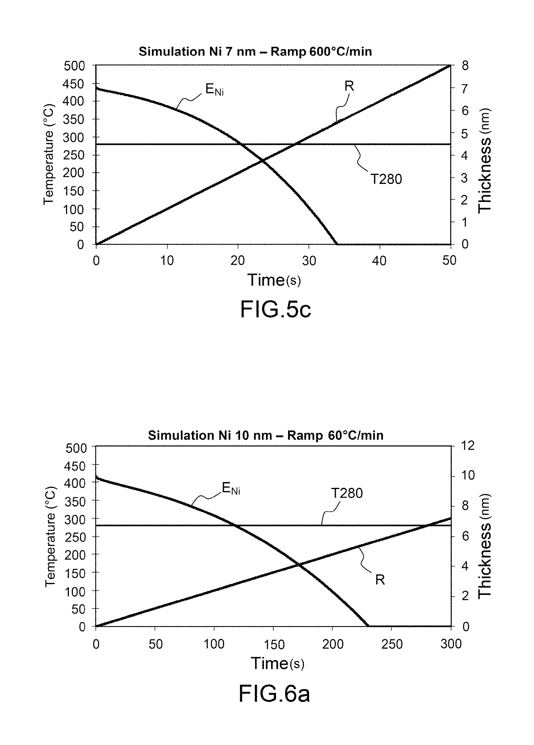
FIGS. 4a and 4b illustrate two options of the invention with one annealing ramp or two annealing ramps, in the case of a 10 nm Ni deposit;
FIGS. 5a-5c illustrate the appearance of the second texture above the nucleation temperature of the second texture, as a function of the annealing rate for an Ni thickness of 7 nm;
FIGS. 6a-6c illustrate the appearance of the second texture above the nucleation temperature of the second texture, as a function of the annealing rate for an Ni thickness of 10 nm;
FIGS. 7a-7c illustrate the appearance of the second texture above the nucleation temperature of the second texture, as a function of the annealing rate for an Ni thickness of 20 nm;
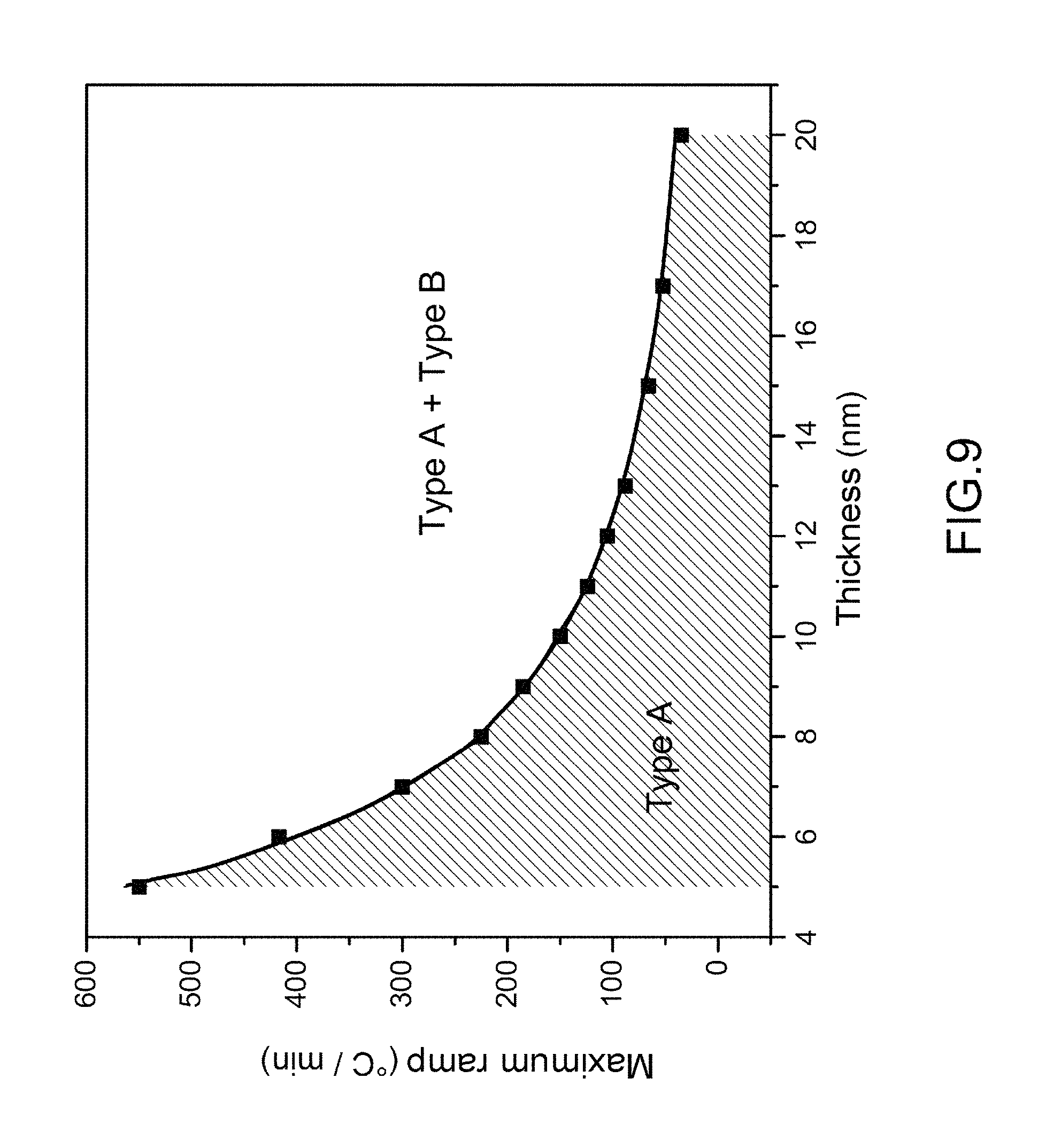
FIGS. 8a-8c generically illustrate the preceding figures, depicting by hatched zones the zones to exclude (zone where the texture B is capable of being formed);
FIG. 9 illustrates the function that the Applicant established, that provides this maximum annealing rate V.sub.max (in .degree. C./min) as a function of the thickness of Ni (in nm);
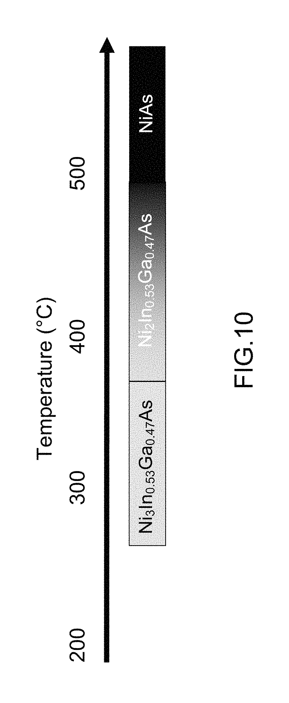
FIG. 10 illustrates the various phases of intermetallic compounds formed as a function of the temperature in the case of a solid reaction between Ni and In.sub.xGa.sub.1-xAs;
FIG. 11 illustrates the change in the lattice parameter of the In.sub.xGa.sub.1-xAs substrate as a function of the indium content (x);
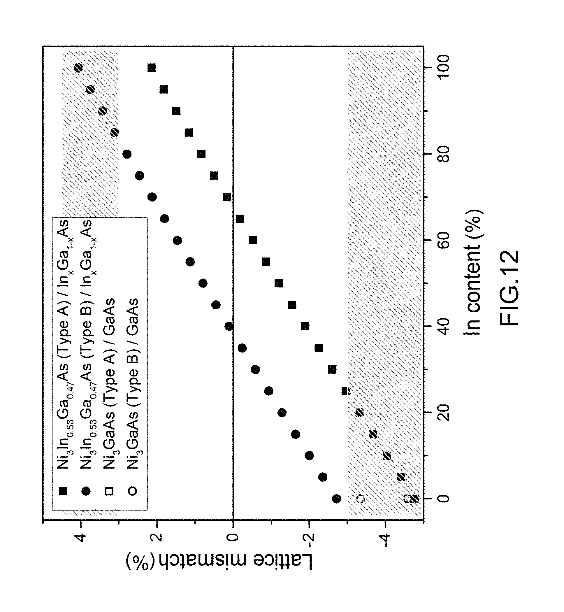
FIG. 12 illustrates the change in the lattice mismatch for the 2 textures of the Ni.sub.3In.sub.0.53Ga.sub.0.47As intermetallic as a function of the indium content of the substrate;
FIG. 13 illustrates the change in the contact sheet resistance of an example of a layer formed of Ni--In.sub.0.53Ga.sub.0.47As as a function of the annealing temperature;
FIG. 14 illustrates the change in the contact resistivity of an example of a layer formed of Ni--In.sub.0.53Ga.sub.0.47As as a function of the annealing temperature.
DETAILED DESCRIPTION
Generally, when an intermetallic contact is produced from the deposition of Ni on the surface of an In.sub.xGa.sub.1-xAs layer or substrate, the solid-state reaction between Ni and In.sub.xGa.sub.1-xAs results in the obtention of several Ni--InGaAs intermetallic compounds having a hexagonal B8 crystallographic structure. Like certain intermetallic compounds, this hexagonal phase has 2 textures (A and B) which are characterized by their orientations relative to the substrate.
For the texture A, the (1010) planes of the intermetallic are parallel to the surface (when the latter is oriented along the (100) planes) of the In.sub.xGa.sub.1-xAs layer or substrate whereas for the texture B it is the (0001) planes which are parallel to the (111) planes of said surface.
This results in the first case in the obtention of a hexagon, the axis c of which is perfectly parallel to the surface of the layer or substrate (texture A) and therefore a perfectly flat Ni--InGaAs/In.sub.xGa.sub.1-xAs interface, and in the other case in a hexagon which is oriented along the (111) planes of the layer or substrate giving a very rough interface that may result in electrical defects (junction breakdown, increase in contact resistivity). This is depicted in FIG. 3.
The Applicant has carried out experiments that make it possible to demonstrate that the texture of the intermetallic compound can be controlled by the thermal budget or the thickness of metal (if the thermal budget has been set) used during the solid-state reaction between the Ni and In.sub.xGa.sub.1-xAs and has concluded that it is advisable to consume all of the Ni before exceeding the nucleation temperature of the texture B. This temperature is between 200.degree. C. and 320.degree. C., with a preference for the range 240.degree. C. and 290.degree. C. according to the content of In in In.sub.xGa.sub.1-xAs.
The annealing time to be applied in order to totally consume the Ni depends on the annealing temperature and on the initial thickness of Ni deposited.
According to present invention, it is proposed to produce nomograms that make it possible to determine, as a function of the initial thickness of Ni and of the annealing temperature, the time required to consume all the Ni.
More specifically, the Applicant has demonstrated the influence of the annealing operation on the formation of the desired texture, without forming the undesirable texture, this being by controlling the temperature rise rate in order to achieve the desired annealing temperature referred to as final annealing temperature, and maintaining this temperature during a hold, this being as a function of the thickness of nickel.
The Applicant has studied two possible annealing options, respectively relating to: an annealing step having a temperature ramp 1 and a hold, corresponding to the simplest option; an annealing step having a ramp 1, followed by a ramp 2 and a hold, corresponding to a more industrializable option.
FIGS. 4a and 4b illustrate these two options, in the case of a 10 nm Ni deposit.
The temperature range of lower contact resistance lies between 300.degree. C. and 350.degree. C.
It is necessary to have obtained a complete consumption of Ni in the range 200.degree. C. and 320.degree. C., with a preference for the range 240.degree. C. and 290.degree. C. to avoid forming the second texture referred to as texture B.
One overall method consists in measuring the thickness of intermetallic compound formed (or of the Ni consumed) as a function of the time for various annealing temperatures. This thickness measurement can be carried out by various characterization methods: by x-ray reflectivity (XRR) analysis, by ellipsometry, microscopy, etc. or any method that makes it possible to extract the thickness of the intermetallic compound and that of the Ni. The thickness L of intermetallic compound formed is generally proportional to the rate of formation D multiplied by the time t, it all being to the power n (n being between 1/2 and 4) as defined below: L=(Dt).sup.n
According to the method described above, it is therefore easily possible to determine the rates of formation for various temperatures and by modeling in order to obtain the time required to completely consume the nickel for a given initial thickness and a given annealing temperature.
Thus, according to this methodology and from data collected from the literature, as described in the publications by J. S. Solomon and S. R. Smith, J. Vac. Sci. Technol. A 5 (1987) 1809 and by H. F. Chuang et al., J. Electron. Mater. 24 (1995) 767,
More specifically, Chuang et al. measure thicknesses of GaAs consumed for a temperature and various times, Solomon and Smith measure Ni concentration gradients as a function of the temperature for a given time. Both deduce therefrom coefficients for diffusion of Ni in GaAs (or rate of formation).
The Applicant carried out various studies to determine the parameters that make it possible to optimize the annealing operation while only forming the first texture A, and avoiding forming the second texture B.
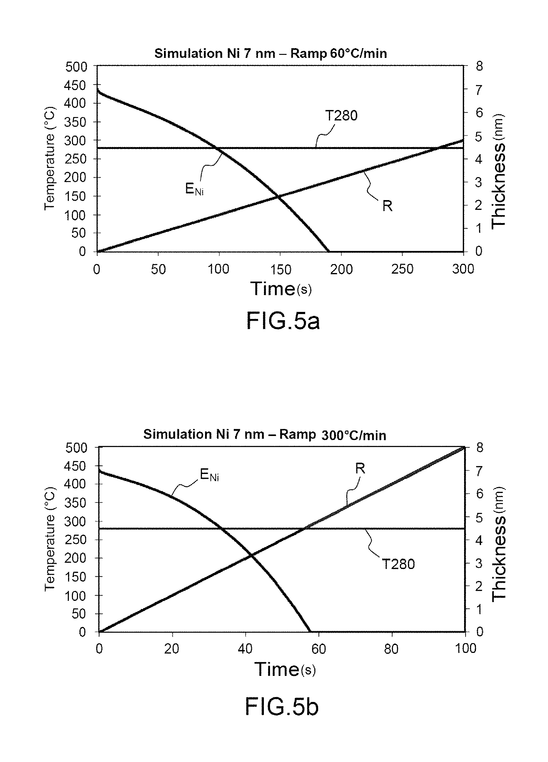
FIGS. 5a-5c, 6a-6c, 7a-7c illustrate the appearance of the second texture above the nucleation temperature of the second texture, as a function of the annealing rate and as a function of the thickness of Ni deposited.
More specifically:
FIGS. 5a-5c relate to an Ni thickness of 7 nm;
FIGS. 6a-6c relate to an Ni thickness of 10 nm;
FIGS. 7a-7c relate to an Ni thickness of 20 nm.
FIGS. 8a-8c generically illustrate the preceding figures, depicting by hatched zones the zones to exclude (zone where the texture B is capable of being formed if nickel is present). More specifically, the curves E.sub.Ni relate to the Ni thickness as a function of time, the straight lines R relate to the temperature ramps.
The horizontal gray hatched band corresponds to the nucleation temperature T.sub.nucl of type B of the second texture.
The hatched zone corresponds to the potential zone where the type of second texture B may grow if it intercepts the curve E.sub.Ni of the Ni before complete consumption.
The curve representing the ramp R should cross the nucleation zone (hatched zone) once all the Ni is consumed (curve E.sub.Ni) in order to favor only the formation of the first texture of type A.
FIG. 8a corresponds to a case 1: with a slow ramp and the formation only of the first texture. FIG. 8b corresponds to a case 2: with a maximum ramp and again the formation only of the first texture.
FIG. 8c corresponds to a case 3: with too fast a ramp and the formation of the first texture A and of the second texture B.
The Applicant was thus able to establish the table below linking the maximum ramps (corresponding to a maximum temperature rise rate) as a function of the thickness.
TABLE-US-00001 Thickness (nm) Maximum ramp (.degree. C./min) 5 550 6 417 7 300 8 225 9 185 10 150 11 124 12 105 13 88 15 66 17 52 20 35
The greater the thickness, the lower the ramp must be and therefore the more a long annealing time is needed.
The function that links the maximum ramp (in .degree. C./min) that can be used with the thickness of Ni deposited (in nm) is a power function: y=12314.7x.sup.-1.91582
The coefficients of this function are dependent on the kinetics of the phase that is formed.
FIG. 9 illustrates the relationship that the Applicant established, that provides this maximum rate V.sub.max (in .degree. C./min) as a function of the thickness of Ni (in nm).
Examples of ramps and hold times are provided below in the case of a single ramp
The Applicant provides ranges of times (it is indicated that the total ramp+hold times do not incorporate the cooling times, the hold time being 60 s). The minimum time typically corresponds to the slope V.sub.max of the maximum case.
For an Ni Thickness of 7 nm:
Minimum time: 70 s
Ramp rate: 300.degree. C./min
Total time: 130 s
For an Ni Thickness of 10 nm:
Minimum time: 140 s
Ramp rate: 150.degree. C./min
Total time: 200 s
For an Ni Thickness of 20 nm:
Minimum time: 600 s
Ramp rate: 35.degree. C./min
Total time: 660 s
Examples of ramps and hold times are provided below in the case of two ramps:
The advantage of a double ramp lies in the fact of reducing the total time of the minimum case (for a given thickness).
For an Ni Thickness of 7 nm:
Minimum time: 56 s
R1 ramp rate: 300.degree. C./min
R2 ramp time: 10 s
Total time: 126 s
For an Ni Thickness of 10 nm:
Minimum time: 112 s
R1 ramp rate: 150.degree. C./min
R2 ramp time: 10 s
Total time: 182 s
For an Ni Thickness of 20 nm:
Minimum time: 480 s
R1 ramp rate: 35.degree. C./min
R2 ramp time: 10 s
Total time: 550 s
The Applicant provides an estimation of the annealing time needed to completely consume a layer of Ni at various annealing temperatures (150, 200, 250 and 300.degree. C.) for the Ni--GaAs system (case where x=0). Specifically, there is a proportionality between the thickness of intermetallic compound and the initial thickness of Ni deposited.
Table 1 below lists all of the results for various initial thicknesses of Ni.
TABLE-US-00002 TABLE 1 Annealing Initial Ni thickness temperature 5 nm 10 nm 50 nm 150.degree. C. 2.8 min 11.2 min 277.4 min 200.degree. C. 1.4 min 5.8 min 140.4 min 250.degree. C. 0.8 min 3.2 min 75.6 min 300.degree. C. 0.6 min 1.8 min 43.2 min
It should be noted that different rates of formation are found depending on the publications that may be explained by the uncertainty regarding the measurement of the thickness and the uncertainty regarding the annealing temperature.
It is therefore necessary to produce these nomograms by taking into account the equipment used.
It has furthermore been reported that the diffusion of Ni in the GaAs compound or the diffusion of Ni in the In.sub.0.53Ga.sub.0.47As compound were very similar in the article by Y. Ashizawa et al., J. Electron. Mater. 25 (1996) 715; this is why it is possible to consider that the orders of magnitude of the preceding data (reported in Table 1) may also be valid, more generally, for the generic Ni--InGaAs intermetallic compound.
According to the present invention, it is therefore proposed to establish nomograms that define, for a given thickness of Ni, the pair of parameters: annealing temperature/annealing time in order to completely consume a given thickness of Ni and to apply these pairs of parameters in order to result in the formation of an intermetallic compound of good texture, i.e. the first texture A having optimal contact surface properties.
According to the process of the present invention, it is thus possible to control the texture making it possible to guarantee the best contact, the metal/semiconductor (In.sub.xGa.sub.1-xAs in the present case) contact resistance being dependent on the Schottky barrier height and therefore on the phase, therefore on the stoichiometry, in contact with the semiconductor.
The Applicant has shown that in the system considered several phases may be formed: Ni.sub.3InGaAs, Ni.sub.2InGaAs, NiAs.
The Applicant is interested in the first phase and the texture A.
Obtaining the texture A is carried out with a small thermal budget and the Ni.sub.3InGaAs phase requires an annealing having a temperature below 350.degree. C. FIG. 10 illustrates, for this purpose, the change in the formation of the various phases that may be obtained during solid reactions in the presence of Ni and In.sub.0.53Ga.sub.0.47As, also referred to as phase sequence.
The Applicant also analyzed the change in the lattice parameter of the In.sub.xGa.sub.1-xAs substrate as a function of the content of indium (x) reported in FIG. 11 in order to estimate a range of favored molar fractions in the composition of the substrate for which the present invention is particularly suitable.
This change is based on the application of Vegard's law between the 2 extreme cases GaAs and InAs and also the intermediate composition In.sub.0.53Ga.sub.0.47As.
With the aid of the straight-line equation taken from figure A, the lattice parameter of the In.sub.xGa.sub.1-xAs substrate was able to be calculated for x varying from 0 to 100 then the interplanar spacing between the (110) and (111) planes was calculated according to the standard formula for a cubic lattice:
##EQU00001##
The results are reported in Table A which provides the value of the interplanar spacings for the (110) and (111) planes of the In.sub.xGa.sub.1-xAs substrate as a function of the content of indium (x).
TABLE-US-00003 TABLE A % In a d(110) d(111) 0 5.6543 3.9981 3.2645 5 5.6743 4.0123 3.2760 10 5.6943 4.0264 3.2876 15 5.7143 4.0406 3.2991 20 5.7343 4.0547 3.3106 25 5.7543 4.0689 3.3222 30 5.7743 4.0830 3.3337 35 5.7943 4.0971 3.3453 40 5.8143 4.1113 3.3568 45 5.8343 4.1254 3.3684 50 5.8543 4.1396 3.3799 55 5.8743 4.1537 3.3915 60 5.8943 4.1678 3.4030 65 5.9143 4.1820 3.4146 70 5.9343 4.1961 3.4261 75 5.9543 4.2103 3.4377 80 5.9743 4.2244 3.4492 85 5.9943 4.2386 3.4608 90 6.0143 4.2527 3.4723 95 6.0343 4.2668 3.4839 100 6.0543 4.2810 3.4954
The Ni.sub.3In.sub.0.53Ga.sub.0.47As/In.sub.0.53Ga.sub.0.47As reference intermetallic has the following lattice parameters (hexagonal lattice): a=3.87 and c=5.03. From these parameters, it is possible to calculate the interplanar spacings for the (1010) and (0001) planes of the intermetallic that correspond respectively to the textures A and B: 3.3515 .ANG. and 5.03 .ANG..
For this reference intermetallic, it is possible to calculate the lattice mismatch for each of the two textures as a function of the indium content of the substrate. This is illustrated by FIG. 12. The lattice mismatch for the texture A is calculated relative to the (110) plane of the substrate. As regards the lattice mismatch for the texture B, it is calculated relative to the (111) plane of the substrate. The larger the absolute value of the lattice mismatch, the lower the probability of forming such and such a texture. Specifically, the increase in the lattice mismatch leads to an increase in the energy difference between the intermetallic and the substrate. Two shaded areas defined on FIG. 6 represent areas where the probability that the texture in question exists is low. Thus, below an indium content of 25%, the probability of forming the texture A is lower and above an indium content of 80%; it is the formation of the texture B that is the least favorable. This figure is constructed from an approximation: it is the Ni.sub.3In.sub.0.53Ga.sub.0.47As reference intermetallic that is used to evaluate the lattice mismatch irrespective of the indium content. Yet the stoichiometry of the intermetallic changes as a function of the indium content of the substrate (for example, the Ni.sub.3In.sub.0.7Ga.sub.0.3As intermetallic is formed on a substrate containing 70% indium). In order to verify that this approximation is valid, two other points were added to FIG. 12, these are lattice mismatch values for the Ni.sub.3GaAs intermetallic on GaAs. The values obtained are relatively similar and in any case are consistent with those obtained for the Ni.sub.3In.sub.0.53Ga.sub.0.47As intermetallic. Thus, despite the approximation made, the "limits" of coexistence of the two textures (25%<x<80%) appear preferential.
Example of a process of the invention comprising the production of an intermetallic contact formed from Ni on an In.sub.0.53Ga.sub.0.47As substrate:
The process comprises the following steps: a step of cleaning the substrate; a step of metal deposition of Ni; one or more annealing steps enabling the formation of an intermetallic compound with the texture A at low temperature and by consuming all the Ni present.
Cleaning Step:
A surface of an In.sub.0.53Ga.sub.0.47As substrate is treated with an HCl:H.sub.2O (1:10 to 1:2, preferentially 1:10) solution for 45 to 60 s in order to remove the native oxides (In.sub.2O.sub.3, Ga.sub.2O.sub.3, As.sub.2O.sub.3, As.sub.2O.sub.5, etc.). The In.sub.0.53Ga.sub.0.47As semiconductor layer is then treated in an cleaning chamber in situ (commonly referred to as a preclean) by an Ar or He plasma in order to remove the possible oxides that might have regrown between the liquid phase (commonly referred to as WET) treatment and the placing of the samples under vacuum before deposition of the metal.
Metal Deposition Step:
Without exposing the sample to air, Ni (7 to 80 nm) is deposited on the In.sub.0.53Ga.sub.0.47As layer. A protective layer which may be TiN (7 nm or more) can advantageously be deposited in order to protect the sample from a possible oxidation at the surface of the metal or at the metal/semiconductor interface.
Annealing Step(s):
The metal layer/semiconductor substrate assembly is treated during an annealing step under a controlled atmosphere. It is the execution of this annealing step that is essential for controlling the texture and the phase of the intermetallic that will be formed.
The Applicant has shown that the intermetallic compound that has the best performance (interface roughness and contact resistivity) may be obtained by means of a one-step or two-step process (with or without complete consumption of the Ni). In the case of 2 steps without complete consumption of the Ni, a step of selective shrinkage is essential.
The first step (low-temperature annealing) makes it possible to control the texture of the intermetallic and therefore the morphology of the interface.
A high-temperature second annealing step makes it possible to optionally change the phase formed during the first step to the least resistive phase without modifying its texture (and therefore the interface morphology).
More specifically, the Applicant has shown that in order to favor the texture that will make the intermetallic compound grow parallel to the substrate (as opposed to the texture that results in a pyramidal material being obtained) it was necessary to heat the sample at low temperature (200.degree. C. and 320.degree. C., with a preference for the range 240.degree. C. and 290.degree. C.) for a long enough time to enable the diffusion and the complete consumption of the Ni (this time depends on the initial Ni layer thickness, it may vary from a few minutes for a 7 nm layer to a few tens of minutes for an 80 nm layer). The Ni.sub.3InGaAs phase is obtained during this annealing.
Once the Ni film is completely consumed, a second annealing of RTA (Rapid Thermal Annealing) type can be carried out in order to control the phase of the intermetallic compound: 250.ltoreq.RTA<350.degree. C. to obtain the Ni.sub.3In.sub.0.53Ga.sub.0.47As phase or 350.ltoreq.RTA<500.degree. C. to obtain the Ni.sub.2In.sub.0.53Ga.sub.0.47As phase. From a contact resistivity point of view, the Ni.sub.3In.sub.0.53Ga.sub.0.47As phase however appears the most favorable. Above 500.degree. C., a rejection of the Ga and In atoms is observed which results in the obtention of InAs clusters which is clearly not favorable in terms of contact resistivity.
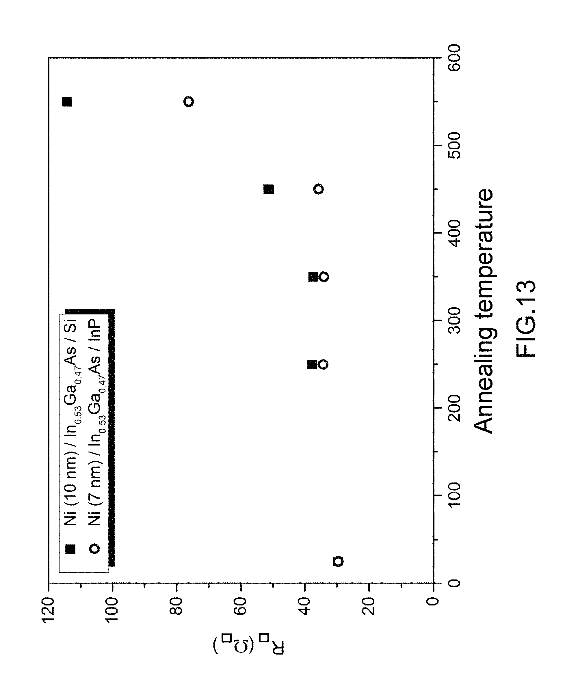
FIG. 13 shows the results of measuring contact sheet resistances as a function of the annealing temperature for: a metal deposition of Ni having an initial thickness of 10 nm on an In.sub.0.53Ga.sub.0.47As on Si stack; a metal deposition of Ni having an initial thickness of 7 nm on an In.sub.0.53Ga.sub.0.47As on InP stack.
It appears that the sheet resistances obtained are actually lower up to annealing temperatures below 500.degree. C., advantageously below 450.degree. C.
FIG. 14 shows the results obtained for the contact resistivity within the context of Ni (20 nm) on an In.sub.0.53Ga.sub.0.47As/InP stack. It also appears that the contact resistivity is low enough with compounds obtained with annealing temperatures below 500.degree. C., advantageously below 450.degree. C.
* * * * *
D00000
D00001
D00002
D00003
D00004
D00005
D00006
D00007
D00008
D00009
D00010
D00011
D00012
D00013
D00014

M00001

XML
uspto.report is an independent third-party trademark research tool that is not affiliated, endorsed, or sponsored by the United States Patent and Trademark Office (USPTO) or any other governmental organization. The information provided by uspto.report is based on publicly available data at the time of writing and is intended for informational purposes only.
While we strive to provide accurate and up-to-date information, we do not guarantee the accuracy, completeness, reliability, or suitability of the information displayed on this site. The use of this site is at your own risk. Any reliance you place on such information is therefore strictly at your own risk.
All official trademark data, including owner information, should be verified by visiting the official USPTO website at www.uspto.gov. This site is not intended to replace professional legal advice and should not be used as a substitute for consulting with a legal professional who is knowledgeable about trademark law.