LED lighting systems and methods
Holec , et al.
U.S. patent number 10,334,735 [Application Number 13/592,090] was granted by the patent office on 2019-06-25 for led lighting systems and methods. This patent grant is currently assigned to Metrospec Technology, L.L.C.. The grantee listed for this patent is Wm. Todd Crandell, Henry V. Holec. Invention is credited to Wm. Todd Crandell, Henry V. Holec.


View All Diagrams
| United States Patent | 10,334,735 |
| Holec , et al. | June 25, 2019 |
LED lighting systems and methods
Abstract
Embodiments of the invention include LED lighting systems and methods. For example, in some embodiments, an LED lighting system is included. The LED lighting system can include a flexible layered circuit structure that can include a top thermally conductive layer, a middle electrically insulating layer, a bottom thermally conductive layer, and a plurality of light emitting diodes mounted on the top layer. The LED lighting system can further include a housing substrate and a mounting structure. The mounting structure can be configured to suspend the layered circuit structure above the housing substrate with an air gap disposed in between the bottom thermally conductive layer of the flexible layered circuit structure and the housing substrate. The distance between the layered circuit structure and the support layer can be at least about 0.5 mm. Other embodiments are also included herein.
| Inventors: | Holec; Henry V. (Mendota Heights, MN), Crandell; Wm. Todd (Minnetonka, MN) | ||||||||||
|---|---|---|---|---|---|---|---|---|---|---|---|
| Applicant: |
|
||||||||||
| Assignee: | Metrospec Technology, L.L.C.
(Mendota Heights, MN) |
||||||||||
| Family ID: | 48426770 | ||||||||||
| Appl. No.: | 13/592,090 | ||||||||||
| Filed: | August 22, 2012 |
Prior Publication Data
| Document Identifier | Publication Date | |
|---|---|---|
| US 20130128582 A1 | May 23, 2013 | |
Related U.S. Patent Documents
| Application Number | Filing Date | Patent Number | Issue Date | ||
|---|---|---|---|---|---|
| 13158149 | Jun 10, 2011 | 8851356 | |||
| 12372499 | Feb 17, 2009 | 7980863 | |||
| 13592090 | |||||
| 13190639 | Jul 26, 2011 | 8500456 | |||
| 12406761 | Mar 18, 2009 | 8007286 | |||
| 13592090 | |||||
| 13411322 | Mar 2, 2012 | 8525193 | |||
| 12043424 | Mar 6, 2008 | 8143631 | |||
| 61028779 | Feb 14, 2008 | ||||
| 61037595 | Mar 18, 2008 | ||||
| 61043006 | Apr 7, 2008 | ||||
| Current U.S. Class: | 1/1 |
| Current CPC Class: | H05K 1/189 (20130101); H05K 2201/10106 (20130101); Y10T 29/49124 (20150115); H05K 2201/09063 (20130101) |
| Current International Class: | H05K 1/18 (20060101) |
| Field of Search: | ;257/82,99,721,724,E33.075,E23.099 ;438/28 |
References Cited [Referenced By]
U.S. Patent Documents
| 2697811 | December 1954 | Deming |
| 2731609 | January 1956 | Sobell, III |
| 3028573 | April 1962 | Stoehr |
| 3086189 | April 1963 | Robbins |
| 3270251 | August 1966 | Evans |
| 3401369 | September 1968 | Plamateer |
| 3499098 | March 1970 | Mcgahey et al. |
| 3585403 | June 1971 | Gribbons |
| 3628999 | December 1971 | Schneble, Jr. et al. |
| 3640519 | February 1972 | William et al. |
| 3745091 | July 1973 | Mccormick |
| 4017847 | April 1977 | Burford et al. |
| 4150421 | April 1979 | Nishihara et al. |
| 4173035 | October 1979 | Hoyt |
| 4249303 | February 1981 | Greenwood et al. |
| 4250536 | February 1981 | Barringer et al. |
| 4285780 | August 1981 | Schachter |
| 4388136 | June 1983 | Jacobus et al. |
| 4515304 | May 1985 | Berger |
| 4521969 | June 1985 | Greenwood |
| 4526432 | July 1985 | Cronin et al. |
| 4533188 | August 1985 | Miniet |
| 4618194 | October 1986 | Kwilos |
| 4685210 | August 1987 | King et al. |
| 4761881 | August 1988 | Bora et al. |
| 4795079 | January 1989 | Yamada |
| 4815981 | March 1989 | Mizuno |
| 4842184 | June 1989 | Miller, Jr. |
| 4871315 | October 1989 | Noschese |
| 4950527 | August 1990 | Yamada |
| 4991290 | February 1991 | MacKay |
| 5001605 | March 1991 | Savagian et al. |
| 5041003 | August 1991 | Smith et al. |
| 5093985 | March 1992 | Houldsworth et al. |
| 5103382 | April 1992 | Kondo et al. |
| 5155904 | October 1992 | Majd |
| 5176255 | January 1993 | Seidler |
| 5224023 | June 1993 | Smith et al. |
| 5254910 | October 1993 | Yang |
| 5375044 | December 1994 | Guritz |
| 5404044 | April 1995 | Booth et al. |
| 5440454 | August 1995 | Hashimoto et al. |
| 5478008 | December 1995 | Takahashi |
| 5511719 | April 1996 | Miyake et al. |
| 5563777 | October 1996 | Miki et al. |
| 5575554 | November 1996 | Guritz |
| 5585675 | December 1996 | Knopf |
| 5887158 | March 1999 | Sample et al. |
| 5917149 | June 1999 | Barcley et al. |
| 5920465 | July 1999 | Tanaka |
| 5984691 | November 1999 | Brodsky et al. |
| 6040624 | March 2000 | Chambers et al. |
| 6065666 | May 2000 | Backlund |
| 6089442 | July 2000 | Ouchi et al. |
| 6095405 | August 2000 | Kim et al. |
| 6100475 | August 2000 | Degani et al. |
| 6113248 | September 2000 | Mistopoulos et al. |
| 6130823 | October 2000 | Lauder et al. |
| 6137816 | October 2000 | Kinbara |
| 6199273 | March 2001 | Kubo et al. |
| 6226862 | May 2001 | Neuman |
| 6239716 | May 2001 | Pross et al. |
| 6299337 | October 2001 | Bachl et al. |
| 6299469 | October 2001 | Glovatsky et al. |
| 6310445 | October 2001 | Kashaninejad |
| 6372997 | April 2002 | Hill et al. |
| 6384339 | May 2002 | Neuman |
| 6428189 | August 2002 | Hochstein |
| 6429383 | August 2002 | Sprietsma et al. |
| 6448661 | September 2002 | Kim et al. |
| 6449836 | September 2002 | Miyake et al. |
| 6465084 | October 2002 | Curcio et al. |
| 6481874 | November 2002 | Petroski |
| 6517218 | February 2003 | Hochstein |
| 6555756 | April 2003 | Nakamura et al. |
| 6578986 | June 2003 | Swaris et al. |
| 6580228 | June 2003 | Chen et al. |
| 6589594 | July 2003 | Hembree |
| 6601292 | August 2003 | Li et al. |
| 6651322 | November 2003 | Currie |
| 6657297 | December 2003 | Jewram et al. |
| 6729888 | May 2004 | Imaeda |
| 6746885 | June 2004 | Cao |
| 6784027 | August 2004 | Streubel |
| 6833526 | December 2004 | Sinkunas et al. |
| 6846094 | January 2005 | Luk |
| 6851831 | February 2005 | Karlicek, Jr. et al. |
| 6884313 | April 2005 | Liu et al. |
| 6897622 | May 2005 | Lister |
| 6898084 | May 2005 | Misra |
| 6902099 | June 2005 | Motonishi et al. |
| 6919529 | July 2005 | Franzen et al. |
| 6936855 | August 2005 | Harrah |
| 6963175 | November 2005 | Archenhold et al. |
| 6966674 | November 2005 | Tsai |
| 6991473 | January 2006 | Balcome et al. |
| 6996674 | February 2006 | Chiu et al. |
| 7023147 | April 2006 | Colby et al. |
| 7037114 | May 2006 | Eiger et al. |
| 7086756 | August 2006 | Maxik |
| 7086767 | August 2006 | Sidwell et al. |
| 7114831 | October 2006 | Popovich et al. |
| 7114837 | October 2006 | Yagi et al. |
| 7149097 | December 2006 | Shteynberg et al. |
| 7199309 | April 2007 | Chamberlin et al. |
| 7204615 | April 2007 | Arik et al. |
| 7210818 | May 2007 | Luk et al. |
| 7248245 | July 2007 | Adachi et al. |
| 7253449 | August 2007 | Wu |
| 7256554 | August 2007 | Lys |
| 7262438 | August 2007 | Mok et al. |
| 7263769 | September 2007 | Morimoto et al. |
| 7276861 | October 2007 | Shteynberg et al. |
| 7284882 | October 2007 | Burkholder |
| 7325955 | February 2008 | Lucas et al. |
| 7331796 | February 2008 | Hougham et al. |
| 7341476 | March 2008 | Soeta |
| 7344279 | March 2008 | Mueller et al. |
| 7377669 | May 2008 | Farmer et al. |
| 7377787 | May 2008 | Eriksson |
| 7394027 | July 2008 | Kaluzni et al. |
| 7397068 | July 2008 | Park et al. |
| 7448923 | November 2008 | Uka |
| 7459864 | December 2008 | Lys |
| 7497695 | March 2009 | Uchida et al. |
| 7502846 | March 2009 | McCall |
| 7514880 | April 2009 | Huang et al. |
| 7543961 | June 2009 | Arik et al. |
| 7547124 | June 2009 | Chang et al. |
| 7550930 | June 2009 | Cristoni et al. |
| 7553051 | June 2009 | Brass et al. |
| 7556405 | July 2009 | Kingsford et al. |
| 7556406 | July 2009 | Petroski et al. |
| 7573210 | August 2009 | Ashdown et al. |
| 7583035 | September 2009 | Shteynberg et al. |
| 7598685 | October 2009 | Shteynberg et al. |
| 7656103 | February 2010 | Shteynberg et al. |
| 7665999 | February 2010 | Hougham et al. |
| 7696628 | April 2010 | Ikeuchi et al. |
| 7710047 | May 2010 | Shteynberg et al. |
| 7710050 | May 2010 | Preston et al. |
| 7777236 | August 2010 | Pachler |
| 7800315 | September 2010 | Shteynberg et al. |
| 7806572 | October 2010 | Mcfadden et al. |
| 7810955 | October 2010 | Stimac et al. |
| 7852009 | December 2010 | Coleman et al. |
| 7852300 | December 2010 | Shteynberg et al. |
| 7880400 | February 2011 | Zhou et al. |
| 7888881 | February 2011 | Shteynberg et al. |
| 7902769 | March 2011 | Shteynberg et al. |
| 7902771 | March 2011 | Shteynberg et al. |
| 7943940 | May 2011 | Boonekamp et al. |
| 7952294 | May 2011 | Shteynberg et al. |
| 7956554 | June 2011 | Shteynberg et al. |
| 7977698 | July 2011 | Ling et al. |
| 7980863 | July 2011 | Holec et al. |
| 8004211 | August 2011 | Van Erp |
| 8007286 | August 2011 | Holec et al. |
| 8011806 | September 2011 | Shiraishi et al. |
| 8038329 | October 2011 | Takahasi et al. |
| 8045312 | October 2011 | Shrier |
| 8061886 | November 2011 | Kraus, Jr. et al. |
| 8065794 | November 2011 | En et al. |
| 8067896 | November 2011 | Shteynberg et al. |
| 8075477 | December 2011 | Nakamura et al. |
| 8115370 | February 2012 | Huang |
| 8124429 | February 2012 | Norman |
| 8137113 | March 2012 | Ouchi et al. |
| 8143631 | March 2012 | Crandell et al. |
| 8162200 | April 2012 | Buchwalter et al. |
| 8166650 | May 2012 | Thomas |
| 8210422 | July 2012 | Zadesky |
| 8210424 | July 2012 | Weibezahn |
| 8227962 | July 2012 | Su |
| 8232735 | July 2012 | Shteynberg et al. |
| 8242704 | August 2012 | Lethellier |
| 8253349 | August 2012 | Shteynberg et al. |
| 8253666 | August 2012 | Shteynberg et al. |
| 8264169 | September 2012 | Shteynberg et al. |
| 8264448 | September 2012 | Shteynberg et al. |
| 8410720 | April 2013 | Holec et al. |
| 8500456 | August 2013 | Holec et al. |
| 8525193 | September 2013 | Crandell et al. |
| 8618669 | December 2013 | Furuta |
| 8710764 | April 2014 | Holec et al. |
| 8851356 | October 2014 | Holec et al. |
| 8947389 | February 2015 | Shin et al. |
| 8968006 | March 2015 | Holec et al. |
| 9341355 | May 2016 | Crandell et al. |
| 9357639 | May 2016 | Holec et al. |
| 9474154 | October 2016 | Johansson et al. |
| 9736946 | August 2017 | Holec et al. |
| 2001/0000906 | May 2001 | Yoshikawa et al. |
| 2001/0004085 | June 2001 | Gueissaz |
| 2002/0014518 | February 2002 | Totani et al. |
| 2002/0043402 | April 2002 | Juskey et al. |
| 2002/0094705 | July 2002 | Driscoll et al. |
| 2002/0105373 | August 2002 | Sudo |
| 2002/0148636 | October 2002 | Belke et al. |
| 2002/0179331 | December 2002 | Brodsky et al. |
| 2003/0040166 | February 2003 | Moshayedi |
| 2003/0052594 | March 2003 | Matsui et al. |
| 2003/0072153 | April 2003 | Matsui et al. |
| 2003/0079341 | May 2003 | Miyake et al. |
| 2003/0092293 | May 2003 | Ohtsuki et al. |
| 2003/0094305 | May 2003 | Ueda |
| 2003/0098339 | May 2003 | Totani et al. |
| 2003/0137839 | July 2003 | Lin |
| 2003/0146018 | August 2003 | Sinkunas et al. |
| 2003/0193789 | October 2003 | Karlicek, Jr. |
| 2003/0193801 | October 2003 | Lin et al. |
| 2003/0199122 | October 2003 | Wada et al. |
| 2003/0223210 | December 2003 | Chin |
| 2004/0007981 | January 2004 | Shibata et al. |
| 2004/0055784 | March 2004 | Joshi et al. |
| 2004/0060969 | April 2004 | Imai et al. |
| 2004/0087190 | May 2004 | Miyazawa et al. |
| 2004/0090403 | May 2004 | Huang |
| 2004/0239243 | December 2004 | Roberts et al. |
| 2004/0264148 | December 2004 | Burdick, Jr. et al. |
| 2005/0056923 | March 2005 | Moshayedi |
| 2005/0067472 | March 2005 | Ohtsuki et al. |
| 2005/0133800 | June 2005 | Park et al. |
| 2005/0207156 | September 2005 | Wang et al. |
| 2005/0239300 | October 2005 | Yasumura et al. |
| 2005/0242160 | November 2005 | Nippa et al. |
| 2005/0272276 | December 2005 | Ooyabu |
| 2006/0000877 | January 2006 | Wang et al. |
| 2006/0025023 | February 2006 | Ikeda et al. |
| 2006/0038542 | February 2006 | Park et al. |
| 2006/0128174 | June 2006 | Jang et al. |
| 2006/0181878 | August 2006 | Burkholder |
| 2006/0220051 | October 2006 | Fung et al. |
| 2006/0221609 | October 2006 | Ryan |
| 2006/0245174 | November 2006 | Ashdown et al. |
| 2006/0284640 | December 2006 | Wang et al. |
| 2007/0015417 | January 2007 | Caveney et al. |
| 2007/0054517 | March 2007 | Hidaka et al. |
| 2007/0077688 | April 2007 | Hsu et al. |
| 2007/0157464 | July 2007 | Jeon et al. |
| 2007/0171145 | July 2007 | Coleman et al. |
| 2007/0184675 | August 2007 | Ishikawa et al. |
| 2007/0194428 | August 2007 | Sato et al. |
| 2007/0210722 | September 2007 | Konno et al. |
| 2007/0216987 | September 2007 | Hagood |
| 2007/0217202 | September 2007 | Sato |
| 2007/0252268 | November 2007 | Chew et al. |
| 2007/0257623 | November 2007 | Johnson et al. |
| 2008/0031640 | February 2008 | Fukui |
| 2008/0045077 | February 2008 | Chou et al. |
| 2008/0138576 | June 2008 | Nozu et al. |
| 2008/0143379 | June 2008 | Norman |
| 2008/0160795 | July 2008 | Chen et al. |
| 2008/0191642 | August 2008 | Slot et al. |
| 2008/0232047 | September 2008 | Yamada et al. |
| 2008/0249363 | October 2008 | Nakamura et al. |
| 2008/0254653 | October 2008 | Uka |
| 2008/0310141 | December 2008 | Mezouari |
| 2008/0311771 | December 2008 | Cho |
| 2009/0029570 | January 2009 | Ikeuchi et al. |
| 2009/0079357 | March 2009 | Shteynberg et al. |
| 2009/0103302 | April 2009 | Lin et al. |
| 2009/0117373 | May 2009 | Wisniewski et al. |
| 2009/0140415 | June 2009 | Furuta |
| 2009/0191725 | July 2009 | Vogt et al. |
| 2009/0205200 | August 2009 | Rosenblatt et al. |
| 2009/0226656 | September 2009 | Crandell et al. |
| 2009/0230883 | September 2009 | Haug |
| 2009/0251068 | October 2009 | Holec et al. |
| 2009/0301544 | December 2009 | Minelli |
| 2009/0308652 | December 2009 | Shih |
| 2010/0008090 | January 2010 | Li et al. |
| 2010/0018763 | January 2010 | Barry |
| 2010/0026208 | February 2010 | Shteynberg et al. |
| 2010/0059254 | March 2010 | Sugiyama et al. |
| 2010/0093190 | April 2010 | Miwa et al. |
| 2010/0109536 | May 2010 | Jung et al. |
| 2010/0110682 | May 2010 | Jung et al. |
| 2010/0167561 | July 2010 | Brown et al. |
| 2010/0187005 | July 2010 | Yeh |
| 2010/0213859 | August 2010 | Shteynberg et al. |
| 2010/0220046 | September 2010 | Plotz et al. |
| 2010/0308738 | December 2010 | Shteynberg et al. |
| 2010/0308739 | December 2010 | Shteynberg et al. |
| 2011/0024180 | February 2011 | Ko |
| 2011/0051448 | March 2011 | Owada |
| 2011/0096545 | April 2011 | Chang et al. |
| 2011/0115411 | May 2011 | Shteynberg et al. |
| 2011/0121754 | May 2011 | Shteynberg et al. |
| 2011/0157897 | June 2011 | Liao et al. |
| 2011/0177700 | July 2011 | Jia et al. |
| 2011/0230067 | September 2011 | Champion et al. |
| 2011/0309759 | December 2011 | Shteynberg et al. |
| 2011/0311789 | December 2011 | Loy et al. |
| 2012/0002438 | January 2012 | Gourlay |
| 2012/0014108 | January 2012 | Greenfield et al. |
| 2012/0068622 | March 2012 | Ward |
| 2012/0081009 | April 2012 | Shteynberg et al. |
| 2012/0081018 | April 2012 | Shteynberg et al. |
| 2012/0097784 | April 2012 | Liao et al. |
| 2012/0162990 | June 2012 | Crandell et al. |
| 2012/0188771 | July 2012 | Kraus et al. |
| 2012/0195024 | August 2012 | Kawaguchi et al. |
| 2013/0070452 | March 2013 | Urano et al. |
| 2014/0015414 | January 2014 | Holec et al. |
| 2014/0168982 | June 2014 | Crandell et al. |
| 2014/0197743 | July 2014 | Holec et al. |
| 2015/0173183 | June 2015 | Holec et al. |
| 2015/0189765 | July 2015 | Holec et al. |
| 2017/0055346 | February 2017 | Holec et al. |
| 2018/0063968 | March 2018 | Holec et al. |
| 201242082 | May 2009 | CN | |||
| 201731316 | Feb 2011 | CN | |||
| 102788284 | Nov 2012 | CN | |||
| 0961351 | Dec 1999 | EP | |||
| 2888517 | Jul 2015 | EP | |||
| 2483942 | Mar 2012 | GB | |||
| 01319993 | Dec 1989 | JP | |||
| 05090726 | Apr 1993 | JP | |||
| 05090749 | Apr 1993 | JP | |||
| 2002043737 | Feb 2002 | JP | |||
| 2002117707 | Apr 2002 | JP | |||
| 2005285960 | Oct 2005 | JP | |||
| 2006080227 | Mar 2006 | JP | |||
| 2011169791 | Sep 2011 | JP | |||
| 2011064107 | Mar 2013 | WO | |||
| 2014031567 | Feb 2014 | WO | |||
Other References
|
"Final Office Action", for U.S. Appl. No. 13/158,149, dated Mar. 6, 2013 (11 pages). cited by applicant . "Notice of Allowance", from U.S. Appl. No. 13/190,639, dated Apr. 4, 2013 (12 pages). cited by applicant . "Notice of Allowance", from U.S. Appl. No. 13/411,322, dated May 10, 2013 (29 pages). cited by applicant . "Notice of Allowance", dated Dec. 3, 2012 in co pending U.S. Appl. No. 12/419,879, "Solid State Lighting Circuit and Controls" (17 pages). cited by applicant . "Notice of Allowance", for U.S. Appl. No. 13/190,639, dated Mar. 7, 2013 (10 pages). cited by applicant . "Response to Non-Final Office Action", dated Oct. 1, 2012 in U.S. Appl. No. 13/411,322, "Layered Structure for Use With High Power Light Emitting Diode Systems" (6 pages). cited by applicant . "3M Thermally Conductive Adhesive Transfer Tapes--Technical Data", Electronic Adhesives and Specialties Department, Engineered Adhesives Division, Sep. 2002, (6 pages). cited by applicant . Murray, Cameron T. et al., "3M Thermally Conductive Tapes", 3M Electronic Markets Materials Division, Mar. 2004 (39 pages). cited by applicant . "Custom LUXEON Design Guide", Application Brief AB12, Mar. 2006 (14 pages). cited by applicant . "DERWENT-ACC-No. 1984-298425", corresponds to JP-59-186388A (1984). cited by applicant . "DERWENT-ACC-No. 2010-J09039", corresponds to JP-201 0-153549A (1984). cited by applicant . "DRAGONtape DT6 Data Sheet", Sep. 2007 (4 pages). cited by applicant . "DRAGONtape Product Information Bulletin", 2007 (2 pages). cited by applicant . "DRAGONtape Product Information Bulletin", OSRAM, Nov. 2005 (4 pages). cited by applicant . "File History", for co-pending U.S. Appl. No. 12/372,499, "Printed Circuit Board Flexible Interconnect Design" filed on Feb. 17, 2009 (254 pages). cited by applicant . "File History", for co-pending U.S. Appl. No. 12/406,761, "Printed Circuit Board Interconnect Construction," filed on Mar. 18, 2009 (244 pages). cited by applicant . "Final Office Action", dated Aug. 7, 2012 in U.S. Appl. No. 13/190,639, "Interconnectable Circuit Boards," (25 pages). cited by applicant . "Final Office Action", dated Mar. 15, 2012 in co pending U.S. Appl. No. 12/419,879, "Solid State Lighting Circuit and Controls" (10 pages). cited by applicant . "FLEX Connectors User's Guide", OSRAM Sylvania, Oct. 2007 (6 pages). cited by applicant . "FR406 High Performance Epoxy Laminate and Prepreg", Isola, 2006 (2 pages). cited by applicant . "FR406: High Performance Epoxy Laminate and Prepreg", http://www.isola-group.com/en/products/name/details.shtl?13, Mar. 2008 (1 page). cited by applicant . "High Performance Epoxy Laminate and Prepreg", Isola, Mar. 2007 (3 pages). cited by applicant . "IPC-4101B: Specification for Base Materials for Rigid and Multilayer Printed Boards", Mar. 2006 (109 pages). cited by applicant . "Kapton Polyimide Film", DuPont Electronics, http://www2.dupont.com/Kapton/en_US/index.html, Feb. 2008 (9 pages). cited by applicant . "Linear Products", OSRAM Sylvania, http://www.sylvanaia.com/BusinessProducts/Innovations/LED+Systems/Linear/- , 2004 (1 page). cited by applicant . "LINEARlight Flex & Power Flex LED Systems", OSRAM Sylvania, http://www/sylvania.com/AboutUs/Pressxpress/Innovation/LightingNews(US)/2- 007/USLi, Sep. 2007 (3 pages). cited by applicant . "LINEARlight Flex TOPLED: Flexible LED Strip", Osran Sylvania LED Systems Specification Guide, 2007 (p. 100). cited by applicant . "LINEARlight Power Flex: Flexible High Light Output LED Modules", OSRAM Sylvania, Apr. 2008 (4 pages). cited by applicant . "LINEARlight Power Flex: Flexible LED Strip", Osran Sylvania LED Systems Specification Guide, 2007 (p. 96). cited by applicant . "LINEARlight Power Flex: LM1OP Data Sheet", May 2007 (4 pages). cited by applicant . "Nichia Application Note", Oct. 2003 (p. 5). cited by applicant . "Non Final Office Action", dated Mar. 5, 2012 in co pending U.S. Appl. No. 13/190,639, "Printed Circuit Board Interconnect Construction" (12 pages). cited by applicant . "Non Final Office Action", dated Jul. 26, 2011 in co pending U.S. Appl. No. 12/419,879, "Solid State Lighting Circuit and Controls" (16 pages). cited by applicant . "Non-Final Office Action", dated Aug. 22, 2012 in co-pending U.S. Appl. No. 13/158,149, "Flexible Circuit Board Interconnection and Methods" (27pages). cited by applicant . "Non-Final Office Action", dated Oct. 1, 2012 in U.S. Appl. No. 13/411,322, "Layered Structure for Use With High Power Light Emitting Diode Systems," (18 pages). cited by applicant . "Non-Final Office Action", dated Aug. 3, 2012 in U.S. Appl. No. 12/419,879, "Solid State Lighting Circuit and Controls," (17 pages). cited by applicant . "Notice of Allowance", dated Nov. 26, 2012 in co-pending U.S. Appl. No. 13/190,639, "Printed Circuit Board Interconnect Construction," (15 pages). cited by applicant . "Notice of Allowance", dated Nov. 16, 2011 in co-pending U.S. Appl. No. 12/043,424, "Layered Structure for Use With High Power Light Emitting Diode Systems," (9 pages). cited by applicant . "NUD4001--High Current LED Driver", Semiconductor Components Industries, LLC, http://onsemi.com, Jun. 2006 (8 pages). cited by applicant . "Product Information Bulletin HF2STick XB: Hi-Flux 2nd Generation Module", OSRAM Sylvania, Jan. 2008 (4 pages). cited by applicant . "Response to Final Office Action", dated Mar. 15, 2012 in co-pending U.S. Appl. No. 12/419,879, filed with USPTO Jun. 15, 2012 (8 pages). cited by applicant . "Response to Final Office Action", dated Aug. 7, 2012, in co-pending U.S. Appl. No. 13/190,639, file with USPTO Nov. 7, 2012 (14 pages). cited by applicant . "Response to Non-Final Office Action", dated Aug. 3, 2012 in co-pending U.S. Appl. No. 12/419,879, filed with USPTO Nov. 5, 2012 (7 pages). cited by applicant . "Response to Non-Final Office Action", dated Jul. 26, 2011 in co-pending U.S. Appl. No. 12/419,879, filed with USPTO Dec. 27, 2011 (7 pages). cited by applicant . "Restriction Requirement", dated Sep. 7, 2011 in co-pending U.S. Appl. No. 13/190,639, "Printed Circuit Board Interconnect Construction" (6 pages). cited by applicant . "Specifications for Nichia Chip Type Warm White LED Model: NS6L083T", Nichia Corporation, No. STSE-CC6063A, <Cat.No.060609> (3 pages). cited by applicant . "Specifications for Nichia Chip Type White LED Model: NS6W083AT", Nichia Corporation, No. STSE-CC7134, <Cat.No.070706> (14 pages). cited by applicant . "TechniMask ISR 1000 Series", Technic, Inc., http://www.technic.com/pwb/solderisr1000.htm, 2003 (1 page). cited by applicant . "Thermal Management for LED Applications Solutions Guide", The Bergquist Company (6 pages). cited by applicant . "T-Iam System--Thermally Conductive Circuit Board Materials", http://www.lairdtech.com/pages/products/T-Lam-System.asp, Feb. 2008 (7 pages). cited by applicant . O'Malley, Kleran, "Using the NUD4001 to Drive High Current LEDs", http;//onsemi.com, Feb. 2005 (4 pages). cited by applicant . "Final Office Action," for U.S. Appl. No. 14/015,679, dated Dec. 16, 2014 (19 pages). cited by applicant . "International Search Report and Written Opinion," for PCT/US2013/055658, dated Jan. 15, 2014 (10 pages). cited by applicant . "Non-Final Office Action," for U.S. Appl. No. 13/158,149, dated Jul. 3, 2013 (32 pages). cited by applicant . "Non-Final Office Action," for U.S. Appl. No. 13/944,610, dated Mar. 18, 2014 (2o0 pages). cited by applicant . "Non-Final Office Action," for U.S. Appl. No. 14/015,679, dated Apr. 1, 2014 (7 pages). cited by applicant . "Non-Final Office Action," for U.S. Appl. No. 14/216,182, dated Nov. 26, 2014 (7 pages). cited by applicant . "Notice of Allowance," for U.S. Appl. No. 13/944,610, dated Nov. 18, 2013 (11 pages). cited by applicant . "Notice of Allowance," for U.S. Appl. No. 13/944,610, dated Oct. 31, 2014 (11 pages). cited by applicant . "Notice of Allowance," for U.S. Appl. No. 13/158,149, dated Feb. 11, 2014 (12 pages). cited by applicant . "Notice of Allowance," for U.S. Appl. No. 13/158,149, dated Jun. 6, 2014 (12 pages). cited by applicant . "Notice of Allowance," for U.S. Appl. No. 13/791,228, dated Dec. 10, 2013 (36 pages). cited by applicant . "Response to Final Office Action," for U.S. Appl. No. 12/372,499, dated Oct. 27, 2010 (7 pages). cited by applicant . "Response to Final Office Action," for U.S. Appl. No. 12/406,761 dated Oct. 12, 2010 (10 pages). cited by applicant . "Response to Final Office Action," for U.S. Appl. No. 12/158,149 , dated Jun. 6, 2013 (10 pages). cited by applicant . "Response to Non-Final Office Action," for U.S. Appl. No. 13/158,149 dated Feb. 21, 2013 (12 pages). cited by applicant . "Response to Non-Final Office Action," for U.S. Appl. No. 13/160,639 dated Jul. 26, 2012 (17 pages). cited by applicant . "Response to Non-Final Office Action," for U.S. Appl. No. 13/158,149, dated Jan. 2, 2014 (14 pages). cited by applicant . "Response to Non-Final Office Action," for U.S. Appl. No. 13/944,610, dated Mar. 18, 2014 and filed with the USPTO Sep. 18, 2014 (9 pages). cited by applicant . "Response to Non-Final Office Action," for U.S. Appl. No. 14/015,679, dated Apr. 1, 2014 and filed with the USPTO Oct. 1, 2014 (6 pages). cited by applicant . "Communication Pursuant to Rules 161(1) and 162 EPC," for European Patent Application No. 13763341.8, dated Apr. 7, 2015 (2 pages). cited by applicant . "International Preliminary Report on Patentability," for PCT/US2013/055658, dated Mar. 5, 2015 (7 pages). cited by applicant . "Non-Final Office Action," for U.S. Appl. No. 14/506,251 dated Sep. 29, 2015 (38 pages). cited by applicant . "Non-Final Office Action," for U.S. Appl. No. 14/015,679, dated Jun. 19, 2015 (9 pages). cited by applicant . "Response Non-Final Office Action," for U.S. Appl. No. 14/015,679, dated Jun. 19, 2015 and filed with the USPTO Sep. 18, 2015 (5 pages). cited by applicant . "Response to Final Office Action," for U.S. Appl. No. 14/015,679, dated Dec. 16, 2014 and filed with the USPTO May 15, 2015 (5 pages). cited by applicant . "Final Office Action," for U.S. Appl. No. 14/506,251, dated Mar. 15, 2016 (17 pages). cited by applicant . "Notice of Allowance," for U.S. Appl. No. 14/014,679 dated Jan. 13, 2016 (10 pages). cited by applicant . "Notice of Allowance," for U.S. Appl. No. 14/015,679 dated Oct. 26, 2015 (10 pages). cited by applicant . "Notice of Allowance," for U.S. Appl. No. 14/633,726, dated Jan. 25, 2016 (35 pages). cited by applicant . "Response to Non-Final Office Action," for U.S. Appl. No. 14/506,251 dated Sep. 29, 2015 and filed with the USPTO Jan. 27, 2016 (10 pages). cited by applicant . "Non-Final Office Action," for U.S. Appl. No. 15/165,678, dated Jan. 20, 2017 (31 pages). cited by applicant . "Response to Non-Final Office Action," for U.S. Appl. No. 14/506,251, dated Dec. 9, 2016 and filed with the USPTO Mar. 23, 2017 (6 pages). cited by applicant . "Non-Final Office Action," for U.S. Appl. No. 14/506,251 dated Dec. 9, 2016 (11 pages). cited by applicant . "Response to Final Office Action," for U.S. Appl. No. 14/506,251, dated Mar. 15, 2016 and filed with the USPTO Sep. 15, 2016 (10 pages). cited by applicant . "Final Office Action," for U.S. Appl. No. 15/165,678 dated Jul. 11, 2018 (10 pages). cited by applicant . "Response to Non-Final Office Action," for U.S. Appl. No. 15/165,678, filed with the USPTO May 30, 2018 (17 pages) for Non-Final Office Action dated Feb. 16, 2018. cited by applicant . "Final Office Action," for U.S. Appl. No. 15/165,678 dated Jul. 31, 2017 (13 pages). cited by applicant . "Response to Non-Final Office Action," for U.S. Appl. No. 15/165,678, mailed Jan. 20, 2017 and filed with the USPTO Jul. 20, 2017 (10 pages). cited by applicant . "Non-Final Office Action," for U.S. Appl. No. 15/165,678 dated Feb. 16, 2018 (22 pages). cited by applicant . "Response to Final Office Action," for U.S. Appl. No. 15/165,678, dated Jul. 31, 2017 and filed with the USPTO Jan. 18, 2018 (12 pages). cited by applicant . "Non-Final Office Action," for U.S. Appl. No. 15/165,678 dated Oct. 18, 2018 (10 pages). cited by applicant . "Non-Final Office Action," for U.S. Appl. No. 15/675,938 dated Oct. 9, 2018 (40 pages). cited by applicant . "Response to Non-Final Office Action," for U.S. Appl. No. 15/165,678 filed with the USPTO Jan. 2, 2019 (10 pages). cited by applicant . "Response to Non-Final Office Action," for U.S. Appl. No. 15/675,938 filed with the USPTO Jan. 2, 2019 (10 pages). cited by applicant . "Final Office Action," for U.S. Appl. No. 15/165,678 dated Mar. 12, 2019 (16 pages). cited by applicant . "Final Office Action," for U.S. Appl. No. 15/675,938 dated Feb. 20, 2019 (17 pages). cited by applicant. |
Primary Examiner: Karimy; Timor
Attorney, Agent or Firm: Pauly, DeVries Smith & Deffner LLC
Parent Case Text
This application is a continuation-in-part of U.S. application Ser. No. 13/158,149, filed Jun. 10, 2011, now U.S. Pat. No. 8,851,356 which is a continuation-in-part of U.S. application Ser. No. 12/372,499, filed Feb. 17, 2009, now U.S. Pat. No. 7,980,863, which claims the benefit of U.S. Provisional Application No. 61/028,779, filed Feb. 14, 2008, and U.S. Provisional Application No. 61/037,595, filed on Mar. 18, 2008, the contents of all of which are herein incorporated by reference. This application is also a continuation-in-part of U.S. application Ser. No. 13/190,639, filed Jul. 26, 2011, now U.S. Pat. No. 8,500,456 which is a continuation of U.S. application Ser. No. 12/406,761, filed Mar. 18, 2009, now U.S. Pat. No. 8,007,286, which claims the benefit of U.S. Provisional Application No. 61/037,595, filed on Mar. 18, 2008, and U.S. Provisional Application No. 61/043,006, filed Apr. 7, 2008, the contents of all of which are herein incorporated by reference. This application is also a continuation-in-part of U.S. application Ser. No. 13/411,322, filed Mar. 2, 2012, now U.S. Pat. No. 8,525,193 which is a continuation of U.S. application Ser. No. 12/043,424, filed Mar. 6, 2008, now U.S. Pat. No. 8,143,631, the contents of all of which are herein incorporated by reference.
Claims
The invention claimed is:
1. An LED lighting system comprising: a flexible layered circuit structure comprising a top thermally conductive layer; a middle electrically insulating layer; a bottom thermally conductive layer; a plurality of light emitting diodes mounted on the top layer; a housing substrate; a mounting structure, the mounting structure comprising an engagement member that grips the flexible layered circuit structure, the mounting structure suspending the layered circuit structure above the housing substrate such that an air gap is disposed in between the bottom thermally conductive layer of the flexible layered circuit structure and the housing substrate, the air gap having a long dimension and a short dimension approximately orthogonal to the long dimension such that the long dimension is longer than the short dimension, where the air gap is open to at least one side of the long dimension of the flexible layered circuit structure, and wherein the distance between the layered circuit structure and the housing substrate is at least about 0.5 mm; and wherein the mounting structure exerts tension outward on the flexible layered circuit structure along the lengthwise axis of the flexible layered circuit structure away from a middle of the flexible layered circuit structure.
2. The LED lighting system of claim 1, further comprising a plurality of light emitting diodes mounted on the bottom layer.
3. The LED lighting system of claim 1, further comprising an optically translucent material layer disposed over the top thermally conductive layer.
4. The LED lighting system of claim 1, wherein the distance between the layered circuit structure and the housing substrate is between about 0.5 mm and 100 mm.
5. The LED lighting system of claim 1, wherein the distance between the layered circuit structure and the housing substrate is between about 40% and 60% of the width of the flexible layered circuit structure.
6. The LED lighting system of claim 1, the mounting structure comprising a tensioner to apply tension to the flexible layered circuit structure.
7. The LED lighting system of claim 6, the tensioner providing a spring force applied to the flexible layered circuit structure.
8. The LED lighting system of claim 7, wherein the tensioner comprises a first spring and a second spring.
9. The LED lighting system of claim 6, the tensioner configured to maintain a tension force of at least one ounce (0.28 N).
10. The LED lighting system of claim 6, the tensioner configured to maintain a tension force of at least one ounce (0.28 N) despite thermal expansion of the flexible layered circuit structure of up to 1 millimeter per meter in length of the flexible circuit structure.
11. The LED lighting system of claim 1, the mounting structure comprising an item selected from the group consisting of a fastener, a hook, a pin, a clip, a spring clip, a tab, and a tab receptacle.
12. The LED lighting system of claim 1, wherein the flexible layered circuit structure has a first end and a second end, wherein the mounting structure engages the first end and the second end.
13. The LED lighting system of claim 12, wherein the flexible layered circuit structure comprises a U shape such that the first end and the second end are disposed adjacent to one another.
14. The LED lighting system of claim 1, wherein the flexible layered circuit structure has a first lateral side and a second lateral side, wherein the mounting structure engages at least one of the first lateral side and the second lateral side.
15. The LED lighting system of claim 1, the housing substrate comprising a material selected from the group consisting of organic and inorganic structural materials.
16. The LED lighting system of claim 1, wherein the light emitting diodes mounted on the top layer have a power of between 0.25 and 3 watts per inch squared of the surface area of the bottom layer.
17. The LED lighting system of claim 1, wherein the flexible circuit structure sufficient flexibility to achieve bending with a radius of curvature of at least 1 inch.
18. The LED lighting system of claim 1, the flexible layered circuit structure defining apertures, the mounting structure configured to engage the apertures to support the flexible layered circuit structure.
19. The LED lighting system of claim 1, the bottom thermally conductive layer comprising a textured surface having a surface area greater than an equally sized substantially flat surface.
20. The LED lighting system of claim 1, the bottom layer covered with a thermally conductive and emissive material.
21. The LED lighting system of claim 1, the housing substrate coated with a material to enhance heat flow across the air gap.
22. The LED lighting system of claim 1, wherein the top layer includes 0.5 to 4.0 ounces per square foot of copper, the intermediate layer includes fiberglass 0.005 to 0.020 inches thick, and the bottom layer includes 0.5 to 4.0 ounces per square foot of copper.
23. The LED lighting system of claim 1, wherein the top, intermediate, and bottom layers have a thermal resistance of less than 10 degrees Celsius per Watt.
24. The LED lighting system of claim 1, configured to have thermal transfer properties sufficient to allow the system to maintain a thermal equilibrium at or below the critical junction temperatures for the LEDs without the addition of secondary heat sinking.
25. The LED lighting system of claim 1, wherein the flexible layered circuit structure is attached to the mounting structure in a releasable manner.
26. The LED lighting system of claim 1, wherein the flexible layered circuit structure is configured for replacement.
27. The LED lighting system of claim 1, wherein the mounting structure supports the layered circuit structure such that the top surface of the layered circuit structure and the bottom surface of the layered circuit structure are substantially open to surrounding air.
28. An LED lighting system comprising: a flexible layered circuit structure comprising a top thermally conductive layer; a middle electrically insulating layer; a bottom thermally conductive layer; a plurality of light emitting diodes mounted on the bottom layer; a housing substrate; a mounting structure suspending the layered circuit structure above the housing substrate by connecting to a top layer of the housing substrate and a bottom layer of the flexible layered circuit structure, where the mounting structure supports the layered circuit structure such that the top surface of the layered circuit structure and the bottom surface of the layered circuit structure are substantially open to surrounding air, and where the top layer of the housing substrate and a bottom layer of the flexible layered circuit structure approximately face one another, with an air gap disposed in between bottom thermally conductive layer of the flexible layered circuit structure and the housing substrate, wherein the distance between the layered circuit structure and the housing substrate is at least about 0.5 mm; and wherein the mounting structure exerts tension on the flexible layered circuit structure in a direction away from the middle of the flexible layered circuit structure along the lengthwise axis of the flexible layered circuit structure such that it is maintained taut.
Description
FIELD OF THE INVENTION
The present invention relates to light emitting diode (LED) lighting system and methods.
BACKGROUND OF THE INVENTION
Solid state lighting (SSL) circuits (or LED lighting systems) are predicted to achieve widespread adoption in commercial lighting applications. Solid state lighting is more efficient in converting electricity to light than incandescent, fluorescent, and compact fluorescent systems. As such solid state lighting stands to greatly increase the energy efficiency of many lighting applications including street lighting, sign lighting, residential lighting, commercial lighting, etc.
SUMMARY OF THE INVENTION
Embodiments of the invention include LED lighting systems and methods. For example, in some embodiments, an LED lighting system is included. The LED lighting system can include a flexible layered circuit structure that can include a top thermally conductive layer, a middle electrically insulating layer, a bottom thermally conductive layer, and a plurality of light emitting diodes mounted on the top layer. The LED lighting system can further include a housing substrate and a mounting structure. The mounting structure can be configured to suspend the layered circuit structure above the housing substrate with an air gap disposed in between the bottom thermally conductive layer of the flexible layered circuit structure and the housing substrate. The distance between the layered circuit structure and the support layer can be at least about 0.5 mm. In some embodiments, the flexible layered circuit structure is attached to the mounting structure in a releasable manner. In some embodiments, the flexible layered circuit structure is releasable from the mounting structure without the use of tools. In some embodiments, the flexible layered circuit structure is configured for replacement.
In some embodiments, an LED lighting system is included. The LED lighting system can include a flexible layered circuit structure can include a top thermally conductive layer, a middle electrically insulating layer, a bottom thermally conductive layer, a plurality of light emitting diodes mounted on the bottom layer, a housing substrate, and a mounting structure. The mounting structure can be configured to suspend the layered circuit structure above the housing substrate with an air gap disposed in between bottom thermally conductive layer of the flexible layered circuit structure and the housing substrate, wherein the distance between the layered circuit structure and the support layer is at least about 0.5 mm.
In some embodiments, a method for making an LED lighting system is included. The method for making an LED lighting system can include obtaining a flexible layered circuit structure that can include, a top thermally conductive layer, a middle electrically insulating layer, a bottom thermally conductive layer. The method can further include suspending the flexible layered circuit structure above a housing substrate with an air gap disposed in between the bottom thermally conductive layer of the flexible layered circuit structure and the housing substrate, wherein the distance between the layered circuit structure and the housing substrate is at least about 0.5 mm, and connecting the flexible layered circuit structure to a power source.
In some embodiments, a method for operating an LED lighting system is included. The method for operating an LED lighting system can include providing electrical current to an LED lighting circuit, the LED lighting circuit including a plurality of light emitting diodes, the LED lighting circuit disposed upon a flexible layered circuit structure can include a top thermally conductive layer, a middle electrically insulating layer, a bottom thermally conductive layer, and dissipating heat from the light emitting diodes to ambient air through the top surface of the top thermally conductive layer and the bottom surface of the bottom thermally conductive layer.
In some embodiments, an LED lighting system is included. The LED lighting system can include a flexible layered circuit structure can include a top thermally conductive layer, a middle electrically insulating layer, a bottom thermally conductive layer, a plurality of light emitting diodes mounted on the top layer, the flexible layered circuit structure formed into a loop. The loop can be disposed within a housing. The loop can be separated from the housing by an air gap. The loop can be disposed sideways to the support structure.
This summary is an overview of some of the teachings of the present application and is not intended to be an exclusive or exhaustive treatment of the present subject matter. Further details are found in the detailed description and appended claims. Other aspects will be apparent to persons skilled in the art upon reading and understanding the following detailed description and viewing the drawings that form a part thereof, each of which is not to be taken in a limiting sense. The scope of the present invention is defined by the appended claims and their legal equivalents.
BRIEF DESCRIPTION OF THE FIGURES
The invention may be more completely understood in connection with the following drawings, in which:
FIG. 1A is a cross sectional schematic view of a flexible layered circuit structure in accordance with various embodiments herein.
FIG. 1B is a cross sectional schematic view of a flexible layered circuit structure in accordance with various embodiments herein.
FIG. 1C is a cross sectional schematic view of a flexible layered circuit structure in accordance with various embodiments herein.
FIG. 1D is a cross sectional schematic view of a flexible layered circuit structure in accordance with various embodiments herein.
FIG. 2 is a schematic side view of a flexible layered circuit structure in accordance with various embodiments herein.
FIG. 3 is a schematic top view of a flexible layered circuit structure in accordance with various embodiments herein.
FIG. 4 is a schematic side view of an LED lighting system in accordance with various embodiments herein.
FIG. 5 is a schematic side view of an LED lighting system in accordance with various embodiments herein.
FIG. 6 is a schematic side view of an LED lighting system in accordance with various embodiments herein.
FIG. 7 is a schematic side view of an LED lighting system in accordance with various embodiments herein.
FIG. 8 is a schematic cut away top view of an LED lighting system in accordance with various embodiments herein.
FIG. 9 is a schematic view of a portion of a mounting structure in accordance with various embodiments herein.
FIG. 10 is a schematic view of a portion of a mounting structure interfaced with a flexible layered circuit structure in accordance with various embodiments herein.
FIG. 11 is a schematic side view of an LED lighting system in accordance with various embodiments herein.
FIG. 12 is a schematic side view of an LED lighting system in accordance with various embodiments herein.
FIG. 13 is a schematic side view of an LED lighting system in accordance with various embodiments herein.
FIG. 14 is a schematic side view of an LED lighting system in accordance with various embodiments herein.
FIG. 15 is a schematic cross sectional view of a flexible layered circuit structure in accordance with various embodiments herein.
FIG. 16 is a schematic cross sectional view of a flexible layered circuit structure in accordance with various embodiments herein.
FIG. 17 is a schematic side view of an LED lighting system in accordance with various embodiments herein.
FIG. 18 is a flowchart of a method of making an LED lighting system in accordance with various embodiments herein.
While the invention is susceptible to various modifications and alternative forms, specifics thereof have been shown by way of example and drawings, and will be described in detail. It should be understood, however, that the invention is not limited to the particular embodiments described. On the contrary, the intention is to cover modifications, equivalents, and alternatives falling within the spirit and scope of the invention.
DETAILED DESCRIPTION OF THE INVENTION
The embodiments of the present invention described herein are not intended to be exhaustive or to limit the invention to the precise forms disclosed in the following detailed description. Rather, the embodiments are chosen and described so that others skilled in the art can appreciate and understand the principles and practices of the present invention.
All publications and patents mentioned herein are hereby incorporated by reference. The publications and patents disclosed herein are provided solely for their disclosure. Nothing herein is to be construed as an admission that the inventors are not entitled to antedate any publication and/or patent, including any publication and/or patent cited herein.
Solid state lighting stands to greatly increase the energy efficiency of many lighting applications including street lighting, sign lighting, residential lighting, commercial lighting, etc. However, one design challenge associated with LED lighting systems is the dissipation of heat. In particular, it is important consider the junction temperature in an LED (the p-n junction temperature) lighting system. If this temperature rises above the prescribed level recommended by the LED manufacturer, the lifetime of the LED as well as its intensity and color may be affected.
Mounting an LED carrying circuit on a heat sink, or adding secondary heat sinks is one approach to heat dissipation. However, this can add additional cost to the finished product in addition to constraining design flexibility. Applicants have developed various embodiments of LED lighting systems that can provide sufficient heat dissipation without the need for directly mounting the LED carrying circuit onto a large heat sink or any substantial secondary heat sinks. Such embodiments can successfully maintain the junction temperature of the LEDs below the critical temperature.
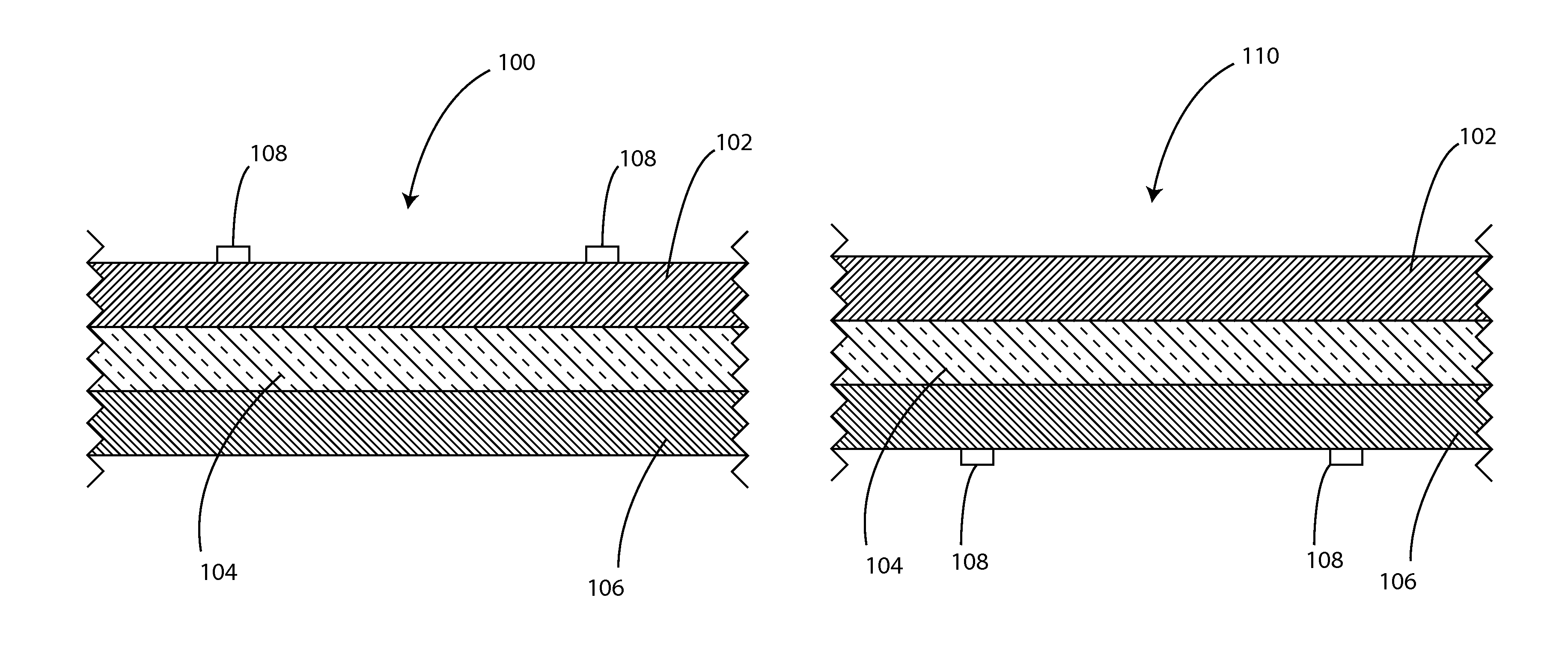
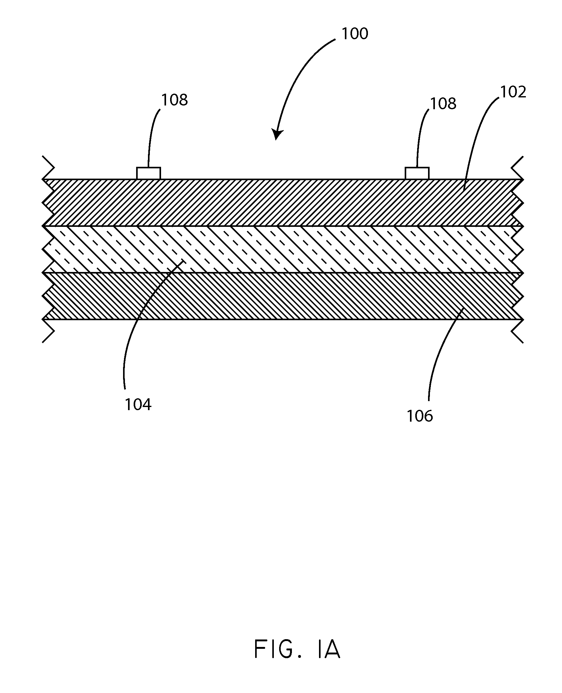
Referring now to FIG. 1A, a cross sectional schematic view is shown of a flexible layered circuit structure 100 in accordance with various embodiments herein. The flexible layered circuit structure can include a top thermally conductive layer 102, a middle electrically insulating layer 104, and a bottom thermally conductive layer 106. In some embodiments, the top, middle, and bottom layers combined have a thermal resistance of less than 10 degrees Celsius per Watt. A plurality of light emitting diodes 108 can be mounted on the top thermally conductive layer 102. When electrical current is passed through the circuit on the top surface of the top thermally conductive layer, one or more of the LEDs can be energized and emit visible light.
In some embodiments, a commercially available FR4 material can be used as a starting material and is modified to create the layered circuit structure. The FR4 material preferably includes a layer of fiberglass sandwiched between two layers of copper. An example of a suitable FR4 material is FR406 manufactured by Isola Group of Chandler, Ariz. The top layer can include one of the two layers of copper, the intermediate layer can include a layer of fiberglass, and the bottom layer can include the other of the two layers of copper. It is recognized that other suitable FR4 materials could be used and that these layers could be either manufactured or purchased in this form.
Prior to modification, the top layer can be copper approximately 0.5 to 4.0 ounces per square foot and approximately 0.0007 to 0.0056 inch thick, 0.25 to 48.00 inches wide, and 0.50 to 48.00 inches long. Although copper is a preferred material, it is recognized that other suitable electrically conductive materials such as but not limited to aluminum could be used. The top, copper layer can be modified to include a thermally conductive printed or etched electrical circuit using standard electrical circuit design tools and techniques well known in the art and can then be coated with a protective coating using standard solder masking and labeling techniques. An example of a suitable protective coating that could be used is TechniMask ISR 1000 manufactured by Technic, Inc. of Cranston, R.I. The top layer can be designed in such a way as to provide receptacles and mounting surfaces for LEDs and other SMT electrical components proximate the top surface.
The intermediate layer can be an electrically insulating thermally conductive layer, in some embodiments made of fiberglass approximately 0.005 to 0.020 inch thick, 0.25 to 48.00 inches wide, and 0.50 to 48.00 inches long. The fiberglass has a breakdown voltage of greater than 5 kilovolts (kV), a tensile strength of 55 kips per square inch (ksi), and a flexural strength of 91 kips per square inch (ksi). The thermal conductivity of the fiberglass can be 0.3 to 0.4 Watts per meter per degrees Kelvin (W/mK). Although fiberglass is a preferred material, it is recognized that other suitable materials such as but not limited to polymer or ceramic blended dielectrics may be used.
Prior to modification, the bottom layer can be copper approximately 0.5 to 4.0 ounces per square foot and can be approximately 0.0007 to 0.0056 inch thick, 0.25 to 48.00 inches wide, and 0.50 to 48.00 inches long. Although copper is a preferred material, it is recognized that other suitable electrically conductive materials such as but not limited to aluminum could be used. The bottom, copper layer can be modified into a heat spreading copper circuit laterally and along its longitudinal axis proximate the bottom surface in order to rapidly spread the heat through the bottom layer. In some embodiments, the exposed copper proximate the bottom surface of the bottom layer can then be tinned. The bottom layer can include thermally conductive printed circuits, which are printed or etched using solder mask printing, photo etching, and solder masking techniques well known in the art for producing electrical circuits. In various embodiments, the bottom layer can include solid coverage of thermally conductive material (such as copper) across an area equal to a majority of the surface area with no direct electrical connection to the top layer.
The flexible layered circuit structure can be at least semi-flexible in some embodiments, not rigid. The flexible layered circuit structure can be any desired length, which could be as long as 250 feet or more. The strip can bend (for example along the lengthwise axis in a direction from the top of the flexible layered circuit structure to the bottom of the flexible layered circuit structure, or bottom to top) sufficiently to achieve a radius of curvature of 6 inches. In some embodiments, the strip can bend sufficiently to achieve a radius of curvature of 1 inch. In some embodiments, the flexible layered circuit structure can be wrapped about the hub of a reel for storage until use. The flexible layered circuit structure can also twist relative to its longitudinal axis up to 10 degrees per inch.
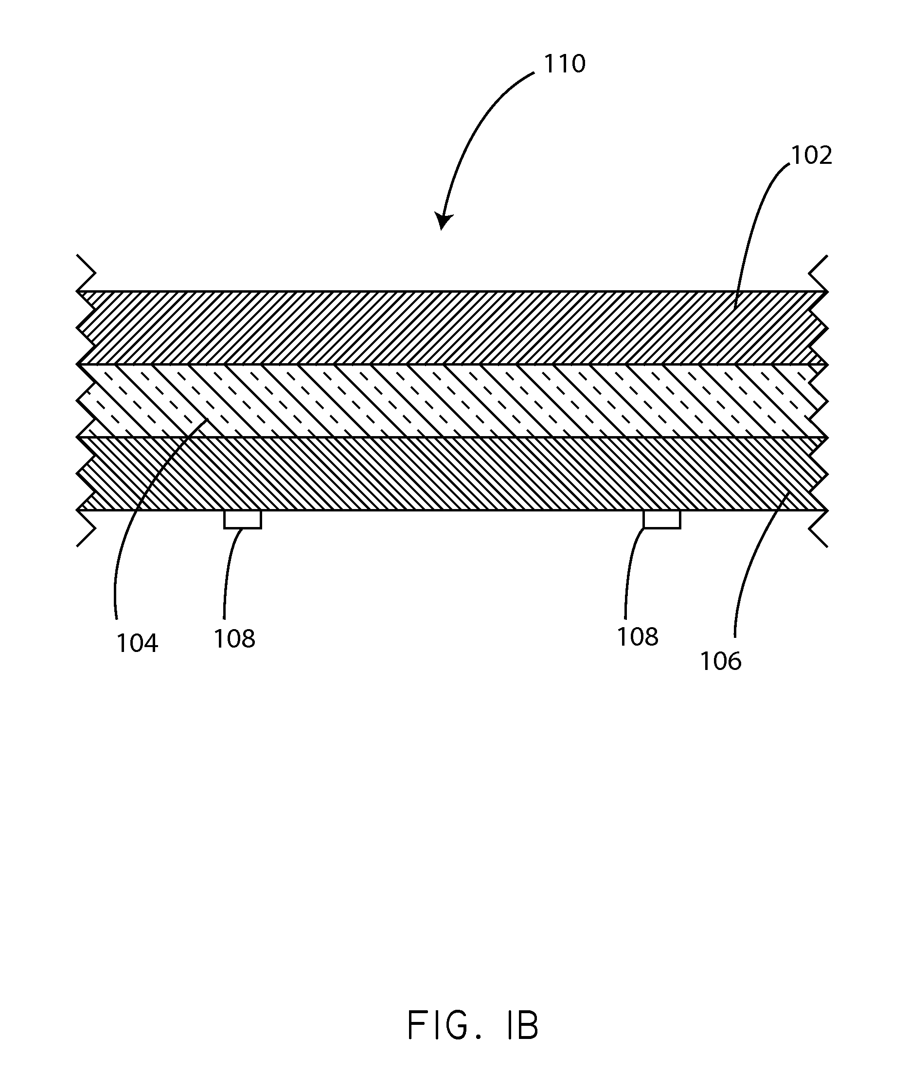
In some embodiments, light emitting diodes can be mounted on the bottom layer of the flexible layered circuit structure. Referring now to FIG. 1B, a cross sectional schematic view is shown of a flexible layered circuit structure 110 in accordance with various embodiments herein. The flexible layered circuit structure 110 can include a top thermally conductive layer 102, a middle electrically insulating layer 104, and a bottom thermally conductive layer 106. A plurality of light emitting diodes 108 can be mounted on the bottom thermally conductive layer 106.
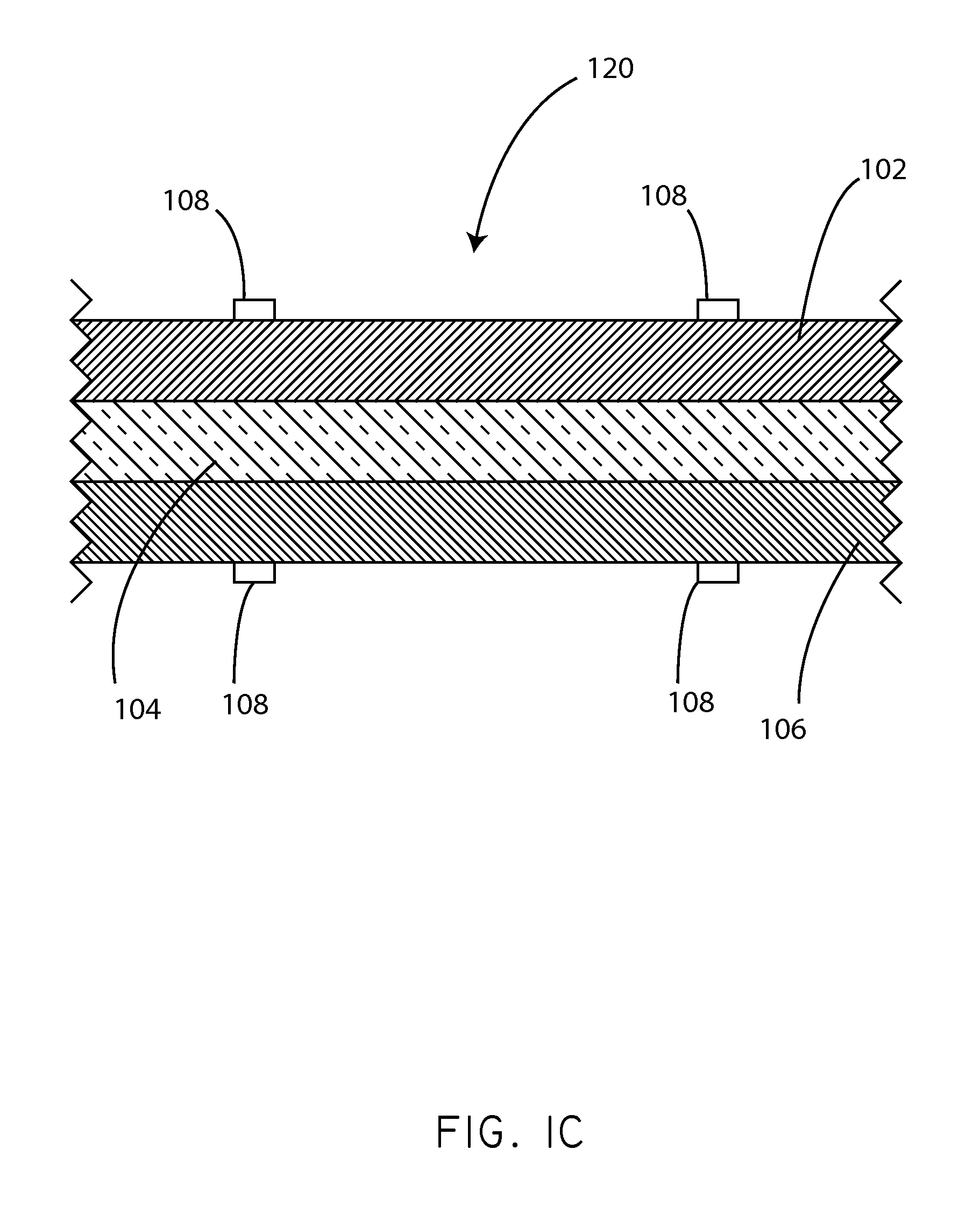
In some embodiments, light emitting diodes can be mounted on both the top and the bottom layers of the flexible layered circuit structure. Referring now to FIG. 1C, a cross sectional schematic view is shown of a flexible layered circuit structure 120 in accordance with various embodiments herein. The flexible layered circuit structure 120 can include a top thermally conductive layer 102, a middle electrically insulating layer 104, and a bottom thermally conductive layer 106. A plurality of light emitting diodes 108 can be mounted on the top thermally conductive layer 102 and the bottom thermally conductive layer 106.
When light emitting diodes are mounted on both the top thermally conductive layer 102 and the bottom thermally conductive layer 106, it will be appreciated that the light emitting diodes can be placed directed opposite on another (such as in FIG. 1C) or they can be offset from one another to avoid the concentration of too much heat in a particular spot. Referring now to FIG. 1D, a cross sectional schematic view is shown of a flexible layered circuit structure 130 in accordance with various embodiments herein. The flexible layered circuit structure 130 can include a top thermally conductive layer 102, a middle electrically insulating layer 104, and a bottom thermally conductive layer 106. A plurality of light emitting diodes 108 can be mounted on the top thermally conductive layer 102 and the bottom thermally conductive layer 106, but offset such that the positions of the light emitting diodes 108 on the top do not match with the positions of the light emitting diodes 108 on the bottom.
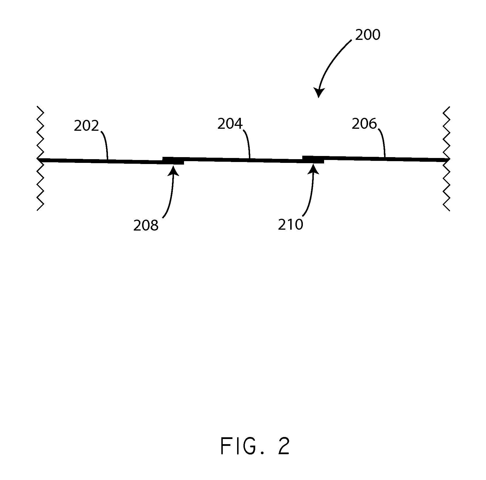
It will be appreciated that flexible layered circuit structures as used in various embodiments herein can be either be unitary segments or can be formed of multiple segments that are bonded to on another at joints. Referring now to FIG. 2, a schematic side view is shown of a flexible layered circuit structure 200 in accordance with various embodiments herein. In this view, it can be seen that the flexible layered circuit structure is formed of a first segment 202, a second segment 204, and a third segment 206. The first segment 202 is bonded to the second segment 204 at a first overlapping joint 208. The first overlapping joint 208 can provide electrical communication between the circuitry on the first segment 202 and the circuitry on the second segment 204. The second segment 204 is bonded to the third segment 206 at a second overlapping joint 210. The second overlapping joint 210 can provide electrical communication between the circuitry on the second segment 204 and the circuitry on the third segment 206. Connections between segments can continue in this manner such that the overall length of the flexible layered circuit structure can be as long as it desired.
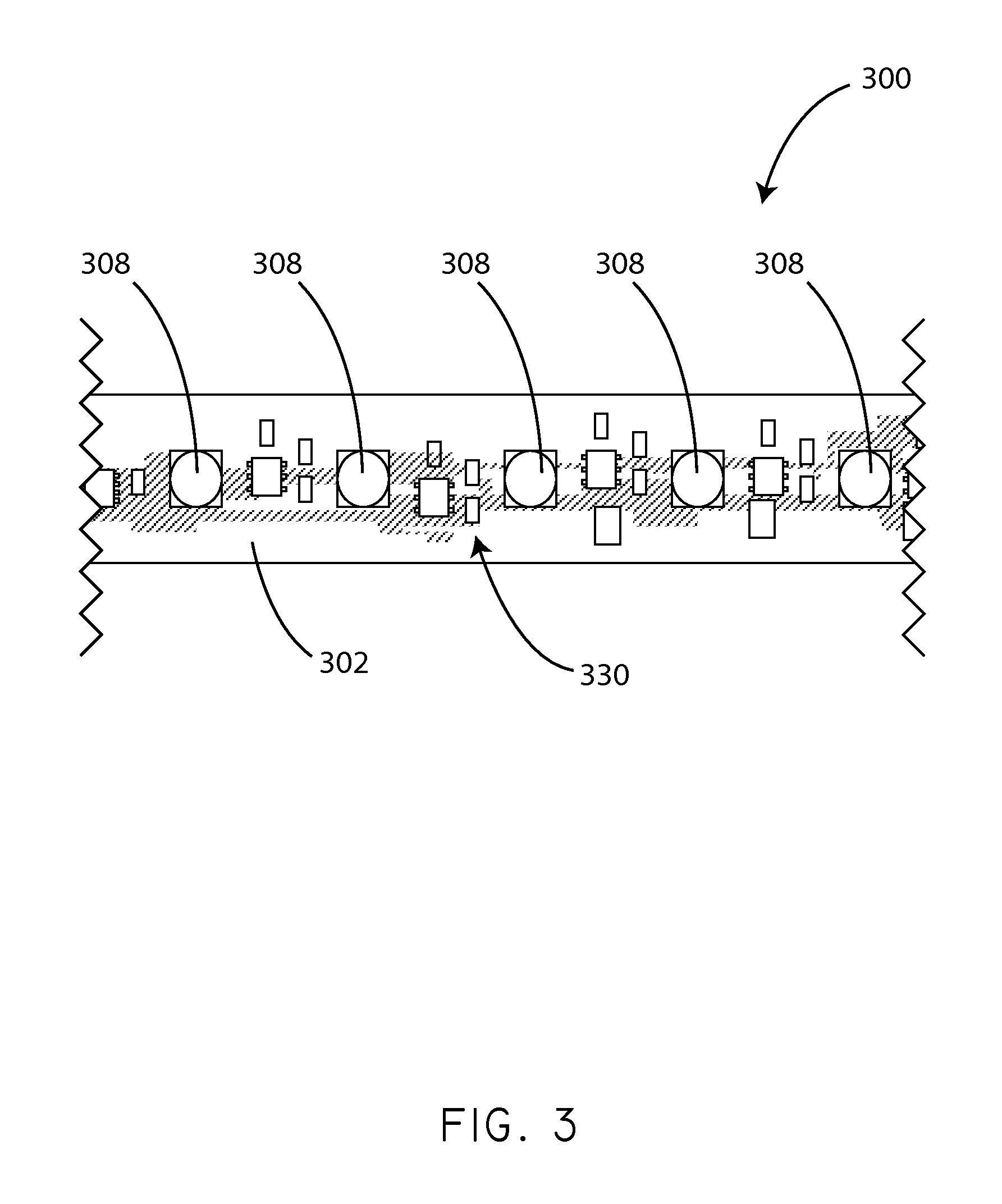
Referring now to FIG. 3, a schematic top view is shown of a portion 300 of the flexible layered circuit structure 200 of FIG. 2. The flexible layered circuit structure includes a top thermally conductive layer 302. A plurality of light emitting diodes 308 are mounted on the top thermally conductive layer 302. A variety of circuitry and/or components 330 can be etched into or mounted on the top thermally conductive layer 302. The circuitry and components 330 can include various items including, but not limited to, resistors, capacitors, traces, linear drivers, and the like. An example of a suitable LED is NS3W083A manufactured by Nichia Corporation of Detroit, Mich. An example of a suitable liner driver is NUD4001 manufactured by ON Semiconductor of Phoenix, Ariz.
In some embodiments, the light emitting diodes mounted on the top layer have a power of between 0.25 and 3 watts per inch squared of the surface area of the bottom layer.
In various embodiments, a mounting structure can be used to suspend the flexible layered circuit structure above a housing substrate. It will be appreciated that the mounting structure can take on many different forms. Referring now to FIG. 4, a schematic side view is shown of an LED lighting system 400 in accordance with various embodiments herein. The LED lighting system 400 can include a flexible layered circuit structure 402 and electrical leads 414 to provide electrical current to the flexible layered circuit structure 402. The flexible layered circuit structure 402 can be suspended above a housing substrate 408, such that there is an air gap 410 disposed in between the bottom thermally conductive layer of the flexible layered circuit structure 402 and the housing substrate 408. In some embodiments, the air gap 410 is present under at least about 80% of the surface area of the bottom of the flexible layered circuit structure 402. A mounting structure can be used to suspend the flexible layered circuit structure. In this embodiment, the mounting structure can include one or more posts 406 or standoffs. The posts 406 can serve to hold the flexible layered circuit structure 402 in place. In some embodiments, the posts can be configured to exert tension on the flexible layered circuit structure in the direction of the lengthwise axis of the flexible layered circuit structure such that it is maintained taut.
The air gap 410 can be of various sizes. In some embodiments, the air gap can be at least about 0.5 mm. In some embodiments, the air gap can be from between 0.5 mm and 100 mm. In some embodiments, the air gap can be from between 1 mm and 50 mm. In some embodiments, the air gap can be from between 2 mm and 25 mm. In some embodiments, the air gap can be between about 40% and 60% of the width of the flexible layered circuit structure.
The air gap can serve to promote heat dissipation off of the bottom layer of the flexible layered circuit structure. In particular, the LED lighting system can be configured so as to have thermal transfer properties sufficient to allow the system to maintain a thermal equilibrium at or below the critical junction temperatures for the LEDs without the need for the addition of secondary heat sinking. The critical junction temperatures can vary based on the specific LED model and manufacturer. However, critical junction temperatures can range from 100 degrees Celsius or less for some LED models to 150 degrees Celsius or more for others. In some embodiments, the junction temperature can be kept below 150 degrees Celsius. In some embodiments, the junction temperature can be kept below 140 degrees Celsius. In some embodiments, the junction temperature can be kept below 130 degrees Celsius. In some embodiments, the junction temperature can be kept below 120 degrees Celsius. In some embodiments, the junction temperature can be kept below 110 degrees Celsius. In some embodiments, the junction temperature can be kept below 100 degrees Celsius. In some embodiments, the junction temperature can be kept below 90 degrees Celsius.
In various embodiments, the mounting structure can include many different specific structural elements. By way of example, in some embodiments, the mounting structure can include a fastener, a hook, a pin, a clip, a spring clip, a tab and/or tab receptacle. In various embodiments, the mounting structure can be directly or indirectly attached to the housing substrate. In some embodiments, the flexible layered circuit structure can be attached to the mounting structure in a releasable manner. In some embodiments, the flexible layered circuit structure can be releasable form the mounting structure in such a way that specialized tools are not required and thus the flexible layered circuit structure can be released from the mounting structure by hand. In this manner, the flexible layered circuit structure can be configured for replacement. In some embodiments, the mounting structure can be used to align the flexible layered circuit structure with secondary optics or a diffuser.
The housing substrate can include many different materials. In some embodiments, the housing substrate can include organic or inorganic structural materials. In some embodiments, the housing substrate can be a material including, but not limited to, metals, polymers, cellulosic materials, composites, glass, stone and the like. In various embodiments, the housing substrate can be opaque, transparent, or semi-transparent.
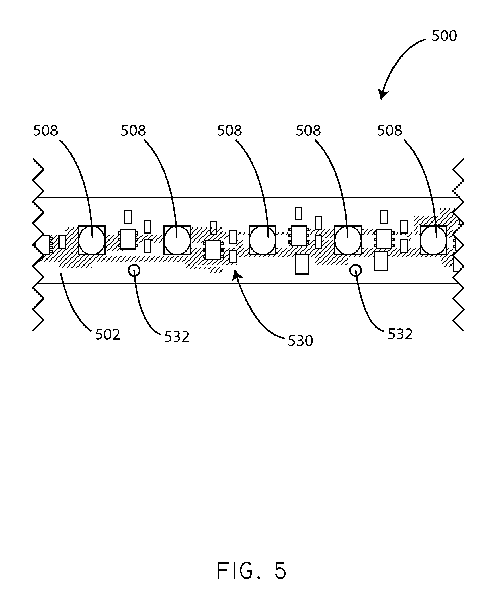
It will be appreciated that the mounting structure can be attached to the flexible layered circuit structure in many different ways. For example, in the context of posts, the posts can attach to the bottom, side, or ends of the flexible layered circuit structure. In some embodiments, the flexible layered circuit structure can include structural features so as to facilitate connection with the mounting structure. By way of example, in some embodiments the flexible layered circuit structure can define notches or apertures in order to facilitate connection with the mounting structure. Referring now to FIG. 5, a schematic top view is shown of a portion of an LED lighting system in accordance with various embodiments herein. The flexible layered circuit structure includes a top thermally conductive layer 502. A plurality of light emitting diodes 508 are mounted on the top thermally conductive layer 502. A variety of circuitry 530 can be etched into or disposed on the top thermally conductive layer 502. In addition, a plurality of apertures 532 are formed in the flexible layered circuit structure. These apertures 532 can be configured to engage a mounting structure, or a portion thereof.
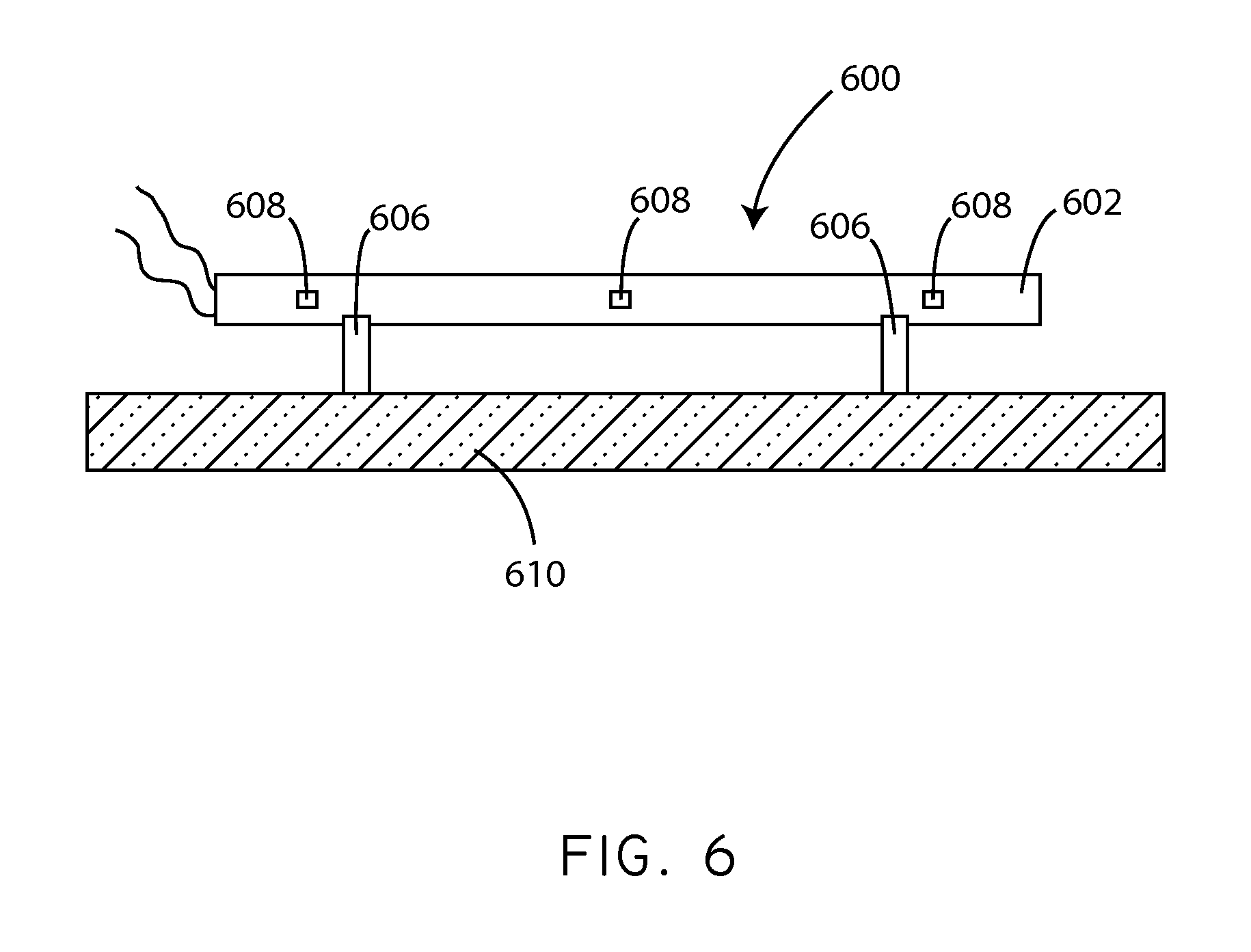
Referring now to FIG. 6, a schematic side view is shown of an LED lighting system 600 in accordance with various embodiments herein. In this embodiment, the flexible layered circuit structure 602 carrying the light emitting diodes 608 is oriented on its side (or lateral side or lateral edge) relative to posts 606, which can serve as a mounting structure to maintain an air gap in between the flexible layered circuit structure 602 and the housing substrate 610. As such, in this embodiment the mounting structure can engage a lateral side of the flexible layered circuit structure.
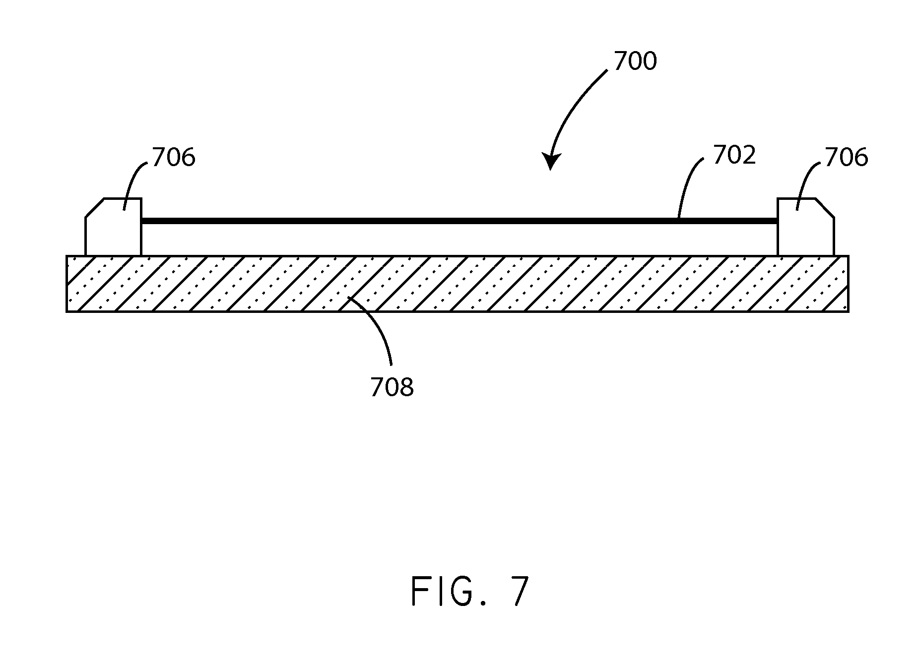
Referring now to FIG. 7, a schematic side view is shown of an LED lighting system 700 in accordance with various embodiments herein. In this view, the flexible layered circuit structure 702 is suspended above the housing substrate through mounting structure elements 706. In this case, the ends of the flexible layered circuit structure interface with the mounting structure elements 706, however, it will be appreciated that other portions of the flexible layered circuit structure 702 can interface with the mounting structure elements 706.
Referring now to FIG. 8, a schematic cut away top view is shown of an LED lighting system 700 in accordance with various embodiments herein. In this view, one example of how the flexible layered circuit structure 702 can be attached to the mounting structure elements 706 is shown. The flexible layered circuit structure 702 can define notches 703 near the ends of the flexible layered circuit structure 702. The mounting structure elements 706 can include an engagement member 710 that passes into the notches 703 in order to grip the flexible layered circuit structure 702. The mounting structure elements 706 can also include a tensioner 712. The tensioner 712 can provide spring force in order to apply tension to the flexible layered circuit structure in order to make it taut. In some embodiments, the tensioner 712 can be configured to maintain a tension force of at least about one ounce (0.28 N). The tensioner 712 can be configured to maintain a tension force on the flexible layered circuit structure despite thermal expansion of the flexible layered circuit structure. By way of example, in some embodiments, the tensioner can be configured to maintain a tension force of at least one ounce (0.28 N) despite thermal expansion of the flexible layered circuit structure of up to 1 millimeter per meter in length of the flexible layered circuit structure. In some embodiments, the tensioner 712 can include a spring. In some embodiments, the mounting structure is used to take up variable length or mechanical tolerances in the construction of the flexible layered circuit structure.
Referring now to FIG. 9, a schematic view of a portion of a mounting structure 800 is shown in accordance with various embodiments herein. The mounting structure 800 can include tabs 824 (or projections). The mounting structure 800 can include a body portion 822 and an aperture 828 to facilitate mounting to another component such as a housing substrate. Referring now to FIG. 10, a schematic view of a portion of a mounting structure 800 interfaced with a flexible layered circuit structure 802 is shown in accordance with various embodiments herein. In this view, it can be seen that the tabs 824 fit within the notches 830 in the flexible layered circuit structure to support it and hold it in place. In addition, the body portion 822 can be capable of being flexed to generate a spring force that can be exerted on the flexible layered circuit structure 802. In this embodiment, the mounting structure for a single end of the flexible layered circuit structure can be formed of a single piece of material, such as a metal or a polymer. However, in other embodiments the mounting structure can include multiple pieces of material.
Referring now to FIG. 11, a schematic side view is shown of an LED lighting system 900 in accordance with various embodiments herein. The LED lighting system 900 can include a flexible layered circuit structure 902. The flexible layered circuit structure 902 can be suspended above a housing substrate 910, such that there is an air gap 914 disposed in between the bottom thermally conductive layer of the flexible layered circuit structure 902 and the housing substrate 910. A mounting structure can be used to suspend the flexible layered circuit structure. In this embodiment, the mounting structure can include one or more blocks 906. The blocks 906 can serve to hold the flexible layered circuit structure 902 in place. In some embodiments, the posts can be configured to exert tension on the flexible layered circuit structure in the direction of the lengthwise axis of the flexible layered circuit structure such that it is maintained taut (e.g., the tension is exerted in a direction away from the middle of the flexible layered circuit structure). In some embodiments, a tensioner 912 can be disposed between the block 906 and the flexible layered circuit structure 902. In this embodiment, for example, the tensioner 912 can include a spring-loaded connection point (such as a hook or tab receptacle) to exert tension on the flexible layered circuit structure 902. In some embodiments, the tensioner 912 can be configured to move with respect to the block 906 in order to apply tension to the flexible layered circuit structure 902. By way of example, the block 906 can move within a channel formed in the block 906.
Referring now to FIG. 12, a schematic side view is shown of an LED lighting system 1000 in accordance with various embodiments herein. The LED lighting system 1000 can include a flexible layered circuit structure 1002. Light emitting diodes 1008 can be mounted on the flexible layered circuit structure 1002. The flexible layered circuit structure 1002 can be suspended inside a cavity defined by a housing substrate 1010. There can be an air gap 1016 disposed in between the flexible layered circuit structure 1002 and the housing substrate 1010. Leads 1014 can be arranged to provide electrical current to the flexible layered circuit structure 1002.
Referring now to FIG. 13, a schematic side view is shown of an LED lighting system 1100 in accordance with various embodiments herein. The LED lighting system 1100 can include a flexible layered circuit structure 1102. Light emitting diodes 1108 can be mounted on the flexible layered circuit structure 1102. In this embodiment, the flexible layered circuit structure 1102 can assume a U shape such that the first end 1118 and the second end 1120 are disposed adjacent to one another. The flexible layered circuit structure 1102 can be suspended inside a cavity defined by a housing substrate 1110. There can be an air gap 1116 disposed in between the flexible layered circuit structure 1102 and the housing substrate 1110. Leads 1114 can be arranged to provide electrical current to the flexible layered circuit structure 1102.
Referring now to FIG. 14, a schematic side view is shown of an LED lighting system 1200 in accordance with various embodiments herein. The LED lighting system 1200 can include a flexible layered circuit structure 1202 and electrical leads to provide electrical current to the flexible layered circuit structure 1202. Material can be disposed over the top of flexible layered circuit structure 1202 (and thus over the top of LEDs in various embodiments) such as optics 1210, secondary optics, or a diffuser. The flexible layered circuit structure 1202 can be suspended above a housing substrate 1208, such that there is an air gap disposed in between the bottom thermally conductive layer of the flexible layered circuit structure 1202 and the housing substrate 1208. A mounting structure can be used to suspend the flexible layered circuit structure. In this embodiment, the mounting structure can include one or more posts 1206 or standoffs.
It will be appreciated that various modifications can be made in order to enhance heat dissipation in the system. By way of example, various modifications can be made to the flexible layered circuit structure in order to enhance heat dissipation. Referring now to FIG. 15, a schematic cross sectional view is shown of a flexible layered circuit structure 1300 in accordance with various embodiments herein. The flexible layered circuit structure can include a top thermally conductive layer 1302, a middle electrically insulating layer 1304, and a bottom thermally conductive layer 1306. A plurality of light emitting diodes 1308 can be mounted on the top thermally conductive layer 1302. A coating 1310 can be disposed on the bottom thermally conductive layer 1306, the coating 1310 comprising a material with properties that enhance heat transfer. For example, in some embodiments, the coating can be a thermally conductive and emissive material. In some embodiments, the coating can be a material such as tinning.
In some embodiments, additional structural features can be disposed on the bottom layer in order to assist in heat dissipation. By way of example, structural features including, but not limited to, heat slugs, cooling fins, heat conductive projections, and the like can be mounted on the bottom surface of the bottom layer in order to aid in heat dissipation.
In some embodiments, the flexible layered circuit structure can be altered in order to enhance heat transfer. Referring now to FIG. 16, a schematic cross sectional view is shown of a flexible layered circuit structure 1400 in accordance with various embodiments herein in accordance with various embodiments herein. The flexible layered circuit structure can include a top thermally conductive layer 1402, a middle electrically insulating layer 1404, and a bottom thermally conductive layer 1406. A plurality of light emitting diodes 1408 can be mounted on the top thermally conductive layer 1402. In this embodiment, the bottom surface 1420 of the bottom thermally conductive layer 1406 can have a surface topology that is different than a standard flat surface. By way of example, the surface can have numerous peaks and valleys (or be textured) in order to increase the surface area.
In some embodiments, the textured surface can have a surface area at least 10 percent greater than an equally sized substantially flat surface. In some embodiments, the textured surface can have a surface area at least 20 percent greater than an equally sized substantially flat surface. In some embodiments, the textured surface can have a surface area at least 30 percent greater than an equally sized substantially flat surface. In some embodiments, the textured surface can have a surface area at least 40 percent greater than an equally sized substantially flat surface. In some embodiments, the textured surface can have a surface area at least 80 percent greater than an equally sized substantially flat surface. In some embodiments, the textured surface can have a surface area at least 100 percent greater than an equally sized substantially flat surface.
Referring now to FIG. 17, a schematic side view is shown of an LED lighting system 1500 in accordance with various embodiments herein. The LED lighting system 1500 can include a flexible layered circuit structure 1502 and electrical leads to provide electrical current to the flexible layered circuit structure 1502. The flexible layered circuit structure 1502 can be suspended above a housing substrate 1508, such that there is an air gap 1510. The top surface 1524 of the housing substrate 1508 can be coated with a layer of material 1522 to enhance heat flow across the air gap 1510.
In some embodiments, a fan can be included to enhance heat dissipation by causing movement of air over surfaces of the flexible layered circuit structure.
It will be appreciated that various methods are also included herein. The method for making an LED lighting system can include obtaining a flexible layered circuit structure that can include, a top thermally conductive layer, a middle electrically insulating layer, a bottom thermally conductive layer. The method can further include suspending the flexible layered circuit structure above a housing substrate with an air gap disposed in between the bottom thermally conductive layer of the flexible layered circuit structure and the housing substrate, wherein the distance between the layered circuit structure and the housing substrate is at least about 0.5 mm, and connecting the flexible layered circuit structure to a power source.
In some embodiments, suspending includes attaching the flexible layered circuit structure to a mounting structure. In some embodiments, the mounting structure provides the connection to the power source. In some embodiments, the method can further include cutting the flexible layered circuit structure to a desired length. In some embodiments, the method can include unwinding the flexible layered circuit structure from a storage reel prior to cutting. In some embodiments, suspending can include attaching the flexible layered circuit structure to a mounting structure that provides a tension force along the length of the flexible layered circuit structure. In some embodiments, the method can further include applying a tension force of at least one ounce (0.28 N) to the flexible layered circuit structure. In some embodiments, the method can further include removing the flexible layered circuit structure from the position suspended above a housing substrate. In some embodiments, the action of removing the flexible layered circuit structure can be accomplished without tools. In some embodiments, the method can further include replacing the flexible layered circuit structure with another flexible layered circuit structure.
Referring now to FIG. 18, a flow chart is shown of a method of making an LED lighting system in accordance with various embodiments herein. The method can include an operation of obtaining a flexible layered circuit structure 1602. Optionally, in some embodiments, the method can further include an operation of cutting the flexible layered circuit structure to a desired length 1604. In various embodiments, the method can further include an operation of suspending the flexible layered circuit structure above a housing substrate 1606. In some embodiments, the method can further include an operation of connecting the flexible layered circuit structure to a power source 1608. Optionally, in some embodiments, the method can include a step of replacing the flexible layered circuit structure with another flexible layered circuit structure 1610. In various embodiments the flexible layer circuit structure can be removed, and optionally replaced, without the use of tools (for example without the need to remove soldering from elements of the system).
In some embodiments, a method for operating an LED lighting system is included. The method for operating an LED lighting system can include providing electrical current to an LED lighting circuit, the LED lighting circuit including a plurality of light emitting diodes, the LED lighting circuit disposed upon a flexible layered circuit structure can include a top thermally conductive layer, a middle electrically insulating layer, and a bottom thermally conductive layer. The method can further include dissipating heat from the light emitting diodes to ambient air through the top surface of the top thermally conductive layer and the bottom surface of the bottom thermally conductive layer.
It should be noted that, as used in this specification and the appended claims, the singular forms "a," "an," and "the" include plural referents unless the content clearly dictates otherwise. It should also be noted that the term "or" is generally employed in its sense including "and/or" unless the content clearly dictates otherwise.
It should also be noted that, as used in this specification and the appended claims, the phrase "configured" describes a system, apparatus, or other structure that is constructed or configured to perform a particular task or adopt a particular configuration to. The phrase "configured" can be used interchangeably with other similar phrases such as arranged and configured, constructed and arranged, constructed, manufactured and arranged, and the like.
All publications and patent applications in this specification are indicative of the level of ordinary skill in the art to which this invention pertains. All publications and patent applications are herein incorporated by reference to the same extent as if each individual publication or patent application was specifically and individually indicated by reference.
The invention has been described with reference to various specific and preferred embodiments and techniques. However, it should be understood that many variations and modifications may be made while remaining within the spirit and scope of the invention.
Further Embodiments
In some embodiments, an LED lighting system is included. The LED lighting system can include a flexible layered circuit structure including a top thermally conductive layer, a middle electrically insulating layer, a bottom thermally conductive layer, and a plurality of light emitting diodes mounted on the top layer. The system can further include a housing substrate and a mounting structure. The mounting structure can be configured to suspend the layered circuit structure above the housing substrate with an air gap disposed in between bottom thermally conductive layer of the flexible layered circuit structure and the housing substrate. The distance between the layered circuit structure and the support layer can be at least about 0.5 mm. The system can further include a plurality of light emitting diodes mounted on the bottom layer. The system can further include an optically translucent material layer disposed over the top thermally conductive layer. The distance between the layered circuit structure and the support layer can be between about 0.5 mm and 100 mm. The distance between the layered circuit structure and the support layer can be between about 40% and 60% of the width of the flexible layered circuit structure. The mounting structure can include a tensioner to apply tension to the flexible layered circuit structure. The tensioner can provide a spring force applied to the flexible layered circuit structure. The tensioner can include a spring. The tensioner can be configured to maintain a tension force of at least one ounce (0.28 N). The tensioner can be configured to maintain a tension force of at least one ounce (0.28 N) despite thermal expansion of the flexible layered circuit structure of up to 1 millimeter per meter in length of the flexible circuit structure. The mounting structure can include a fastener. The mounting structure can include a hook. The mounting structure can include a pin. The mounting structure can include a clip. The mounting structure can include a spring clip. The mounting structure can include a tab or tab receptacle. The mounting structure can be direct or indirectly attached to the housing substrate. The flexible layered circuit structure can include a first end and a second end, wherein the mounting structure engages the first end and the second end. The flexible layered circuit structure can be in a U shape such that the first end and the second end are disposed adjacent to one another. The flexible layered circuit structure can have a first lateral side and a second lateral side, wherein the mounting structure can engage at least one of the first lateral side and the second lateral side. The housing substrate can include a material that can be selected from the group consisting of organic and inorganic structural materials. The housing substrate can include a material that can be selected from the group consisting of a polymer, a cellulosic material, a composite, a glass, and stone. The housing substrate can include a metal. The light emitting diodes mounted on the top layer can have a power of between 0.25 and 3 watts per inch squared of the surface area of the bottom layer. The flexible circuit structure can have sufficient flexibility to achieve bending with a radius of curvature of at least 1 inch. The flexible layered circuit structure can define apertures, the mounting structure can be configured to engage the apertures to support the flexible layered circuit structure. The bottom thermally conductive layer can include a textured surface having a surface area greater than an equally sized substantially flat surface. The bottom thermally conductive layer can include a plurality of heat sink fins mounted thereon. The bottom thermally conductive layer can include a textured surface having a surface area at least 20 percent greater than an equally sized substantially flat surface. The system can further include a coating over the bottom thermally conductive layer, the coating can include a material with properties that enhance heat transfer. The coating can include tinning. The bottom layer can be covered with a thermally conductive and emissive material. The housing substrate can be coated with a material to enhance heat flow across the air gap. The top layer can include 0.5 to 4.0 ounces per square foot of copper, the intermediate layer can include fiberglass 0.005 to 0.020 inches thick, and the bottom layer can include 0.5 to 4.0 ounces per square foot of copper. The top, intermediate, and bottom layers, together, can have a thermal resistance of less than 10 degrees Celsius per Watt. The system can be configured to have thermal transfer properties sufficient to allow the system to maintain a thermal equilibrium at or below the critical junction temperatures for the LEDs without the addition of secondary heat sinking. The flexible layered circuit structure is attached to the mounting structure in a releasable manner. The flexible layered circuit structure can be releasable from the mounting structure without the use of tools. The flexible layered circuit structure can be configured for replacement.
In some embodiments, an LED lighting system is included. The LED lighting system can include a flexible layered circuit structure including a top thermally conductive layer, a middle electrically insulating layer, a bottom thermally conductive layer, a plurality of light emitting diodes mounted on the bottom layer, a housing substrate, and a mounting structure. The mounting structure can be configured to suspend the layered circuit structure above the housing substrate with an air gap disposed in between bottom thermally conductive layer of the flexible layered circuit structure and the housing substrate, wherein the distance between the layered circuit structure and the support layer is at least about 0.5 mm.
In some embodiments, a method for making an LED lighting system is included. The method for making an LED lighting system can include obtaining a flexible layered circuit structure that includes, a top thermally conductive layer, a middle electrically insulating layer, a bottom thermally conductive layer. The method can also include suspending the flexible layered circuit structure above a housing substrate with an air gap disposed in between the bottom thermally conductive layer of the flexible layered circuit structure and the housing substrate, wherein the distance between the layered circuit structure and the housing substrate is at least about 0.5 mm, and connecting the flexible layered circuit structure to a power source. Suspending can include attaching the flexible layered circuit structure to a mounting structure. The mounting structure can provide the connection to the power source. The method can further include cutting the flexible layered circuit structure to a desired length. The method can further include unwinding the flexible layered circuit structure from a storage reel prior to cutting. Suspending can include attaching the flexible layered circuit structure to a mounting structure that provides a tension force along the length of the flexible layered circuit structure. The method can further include applying a tension force of at least one ounce (0.28 N) to the flexible layered circuit structure. The method can further include removing the flexible layered circuit structure from the position suspended above a housing substrate. The step of removing can be accomplished without tools. The method can further include replacing the flexible layered circuit structure with another flexible layered circuit structure.
In some embodiments, a method for operating an LED lighting system is included. The method for operating an LED lighting system can include providing electrical current to an LED lighting circuit, the LED lighting circuit including a plurality of light emitting diodes, the LED lighting circuit disposed upon a flexible layered circuit structure. The flexible layered circuit structure can include a top thermally conductive layer, a middle electrically insulating layer, and a bottom thermally conductive layer. The method can further include dissipating heat from the light emitting diodes to ambient air through the top surface of the top thermally conductive layer and the bottom surface of the bottom thermally conductive layer.
In some embodiments, an LED lighting system is included. The LED lighting system can include a flexible layered circuit structure including a top thermally conductive layer, a middle electrically insulating layer, a bottom thermally conductive layer, and a plurality of light emitting diodes mounted on the top layer. The flexible layered circuit structure can be formed into a loop. The loop can be disposed within a housing. The loop can be separated from the housing by an air gap. The loop can be disposed sideways to the support structure.
* * * * *
References
-
isola-group.com/en/products/name/details.shtl?13
-
www2.dupont.com/Kapton/en_US/index.html
-
sylvanaia.com/BusinessProducts/Innovations/LED+Systems/Linear
-
www/sylvania.com/AboutUs/Pressxpress/Innovation/LightingNews
-
onsemi.com
-
technic.com/pwb/solderisr1000.htm
-
lairdtech.com/pages/products/T-Lam-System.asp
D00000
D00001
D00002
D00003
D00004
D00005
D00006
D00007
D00008
D00009
D00010
D00011
D00012
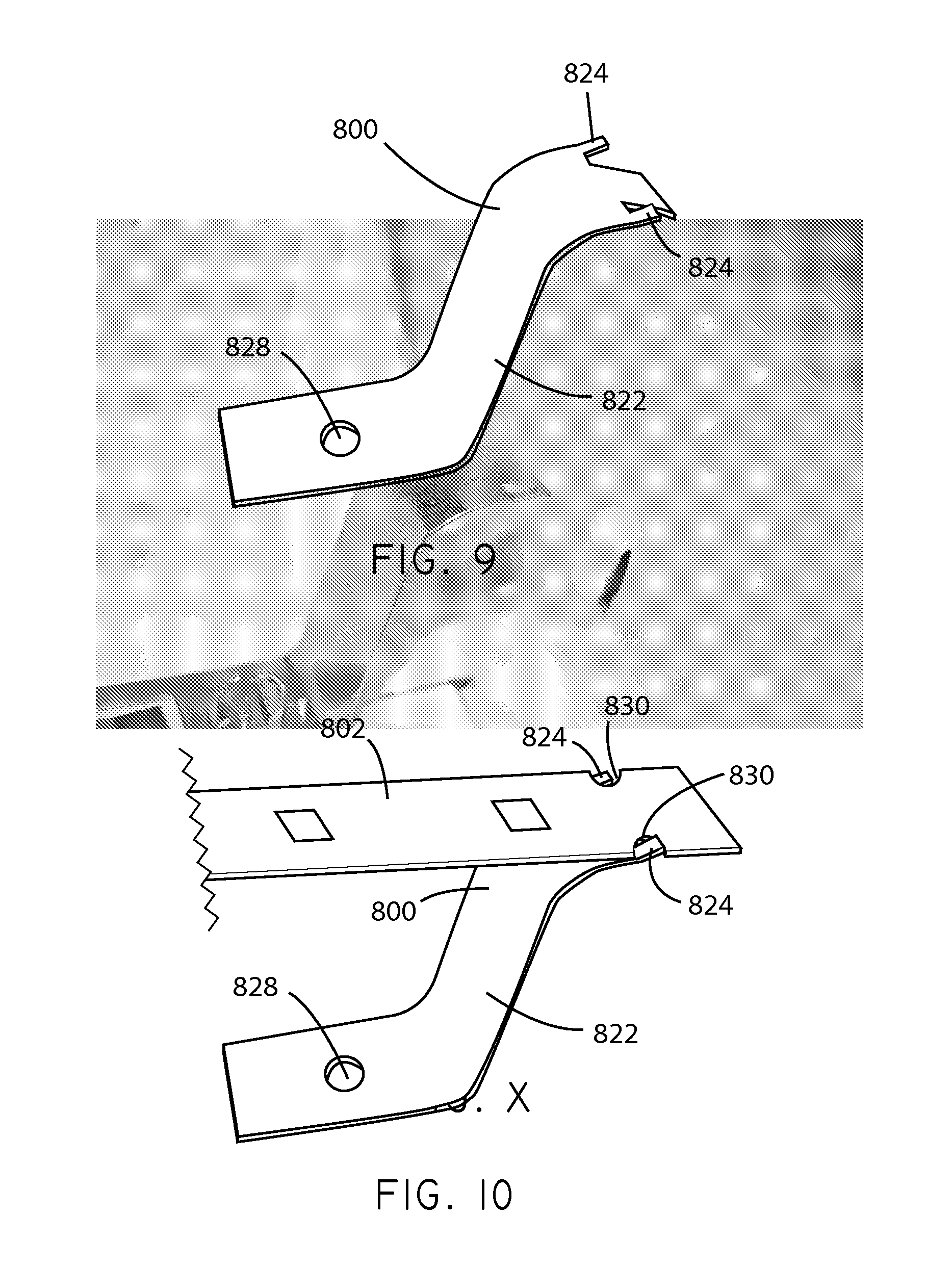
D00013

D00014

D00015
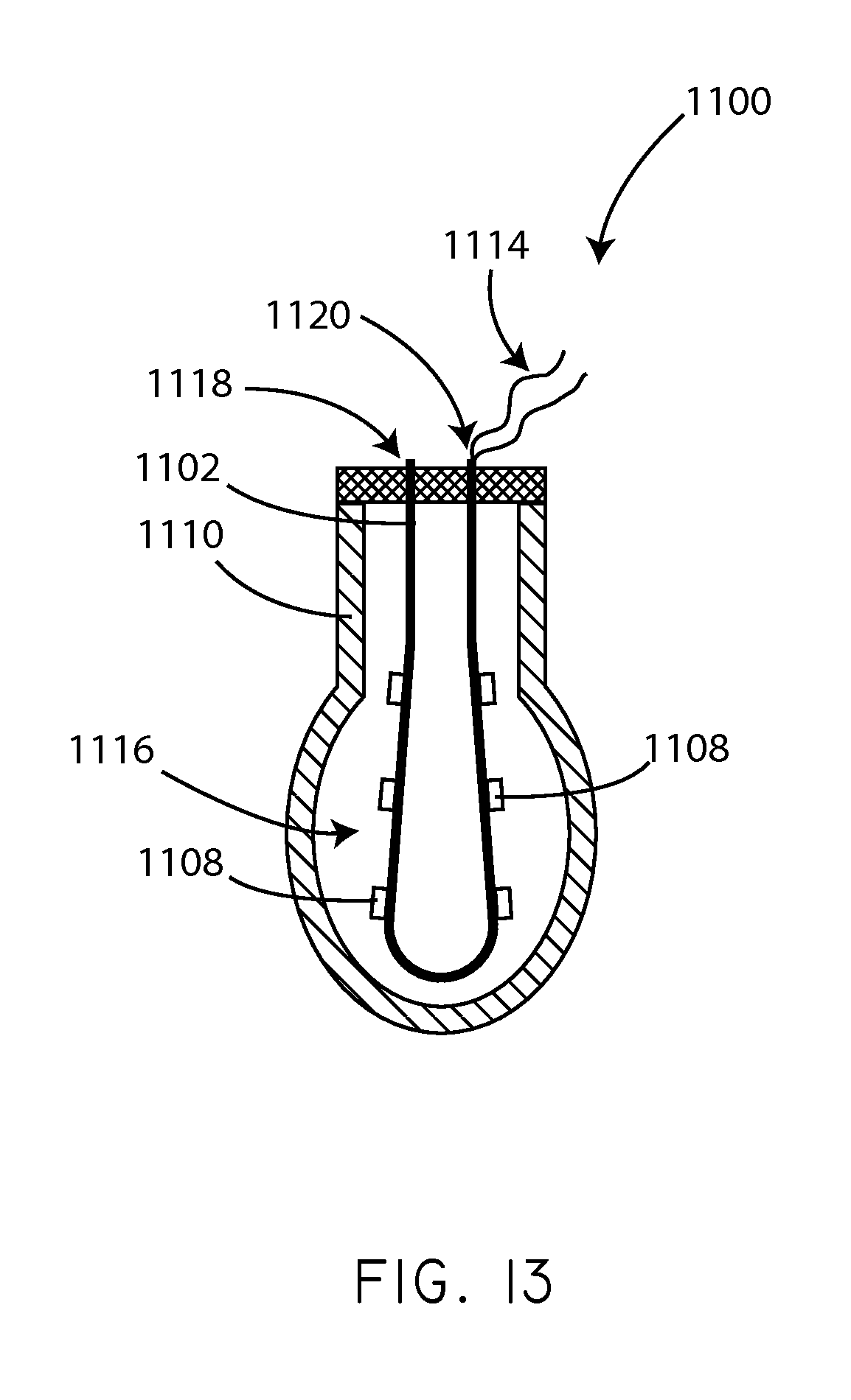
D00016
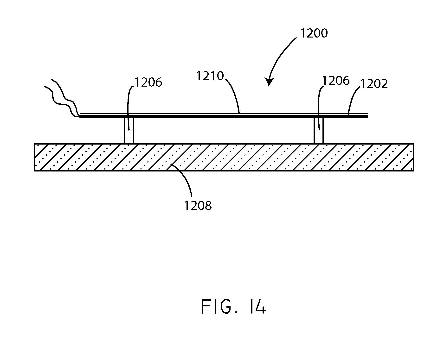
D00017
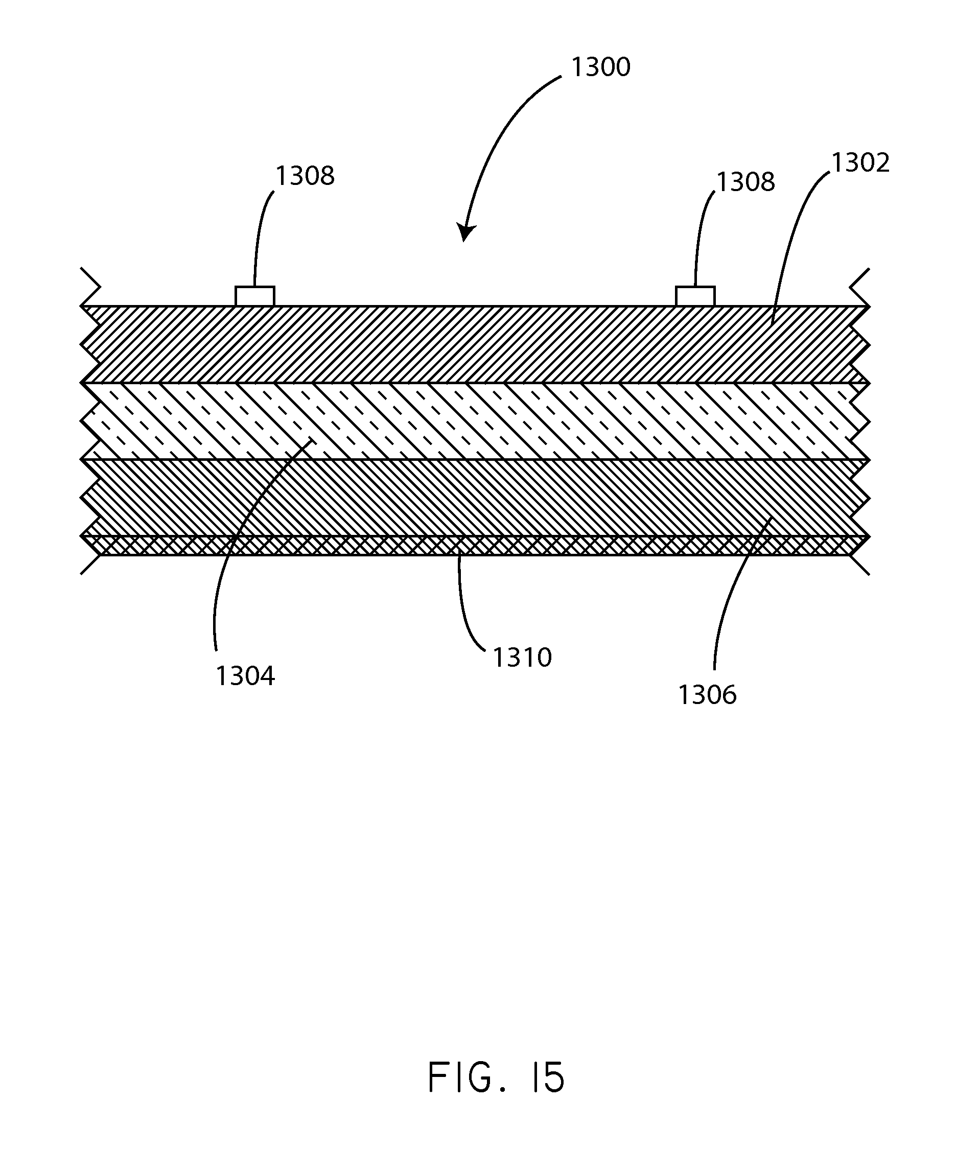
D00018
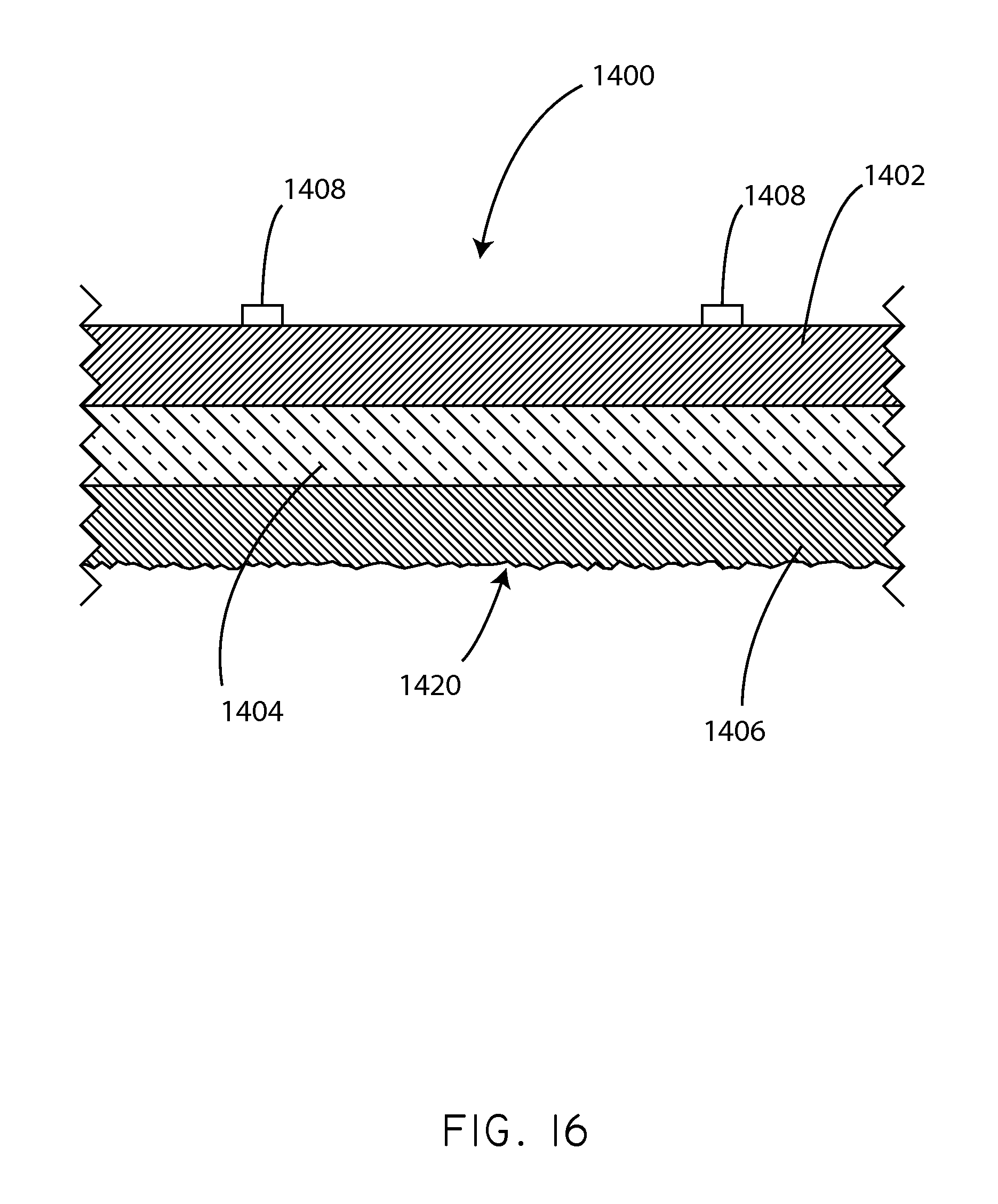
D00019
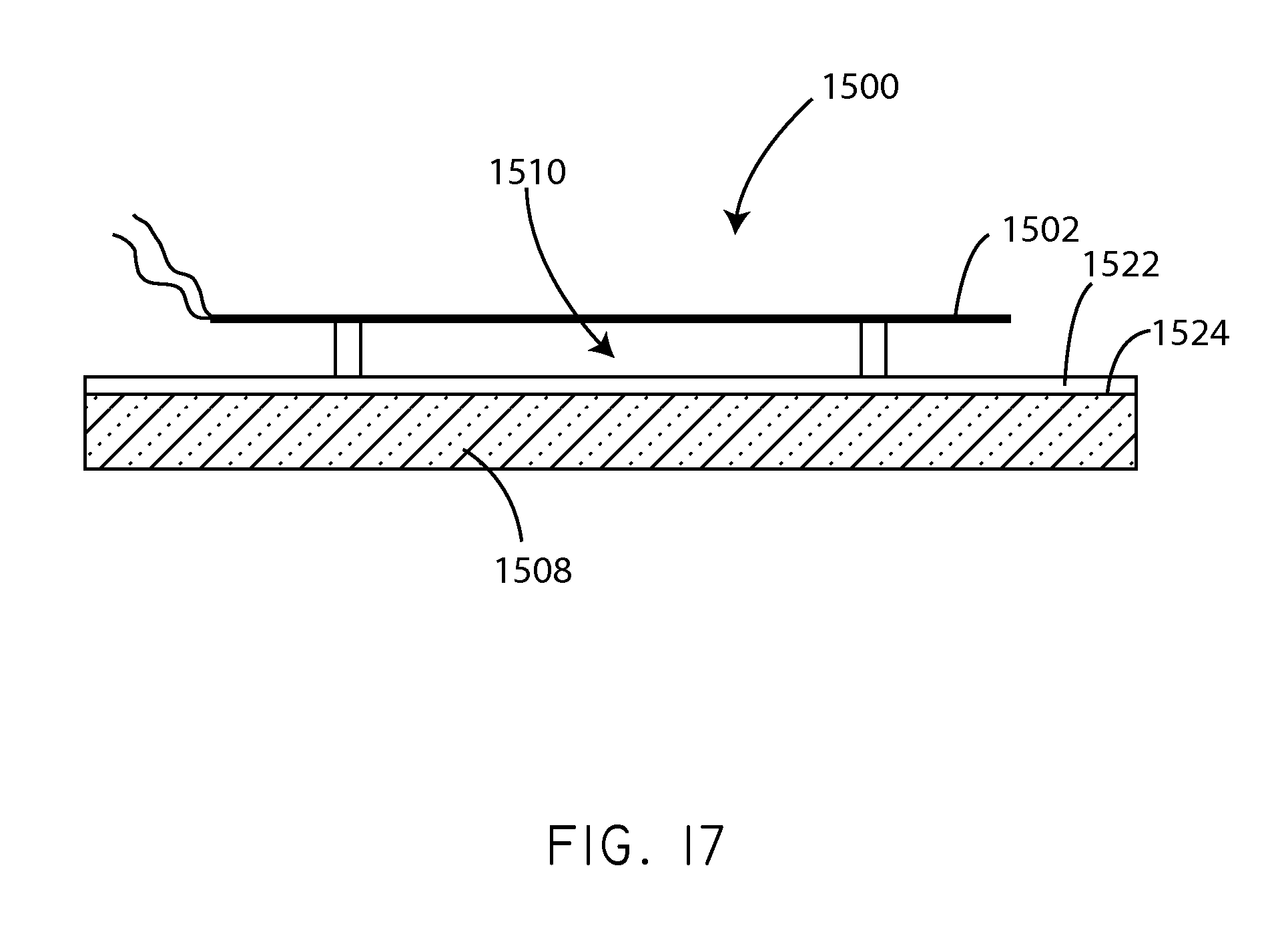
D00020
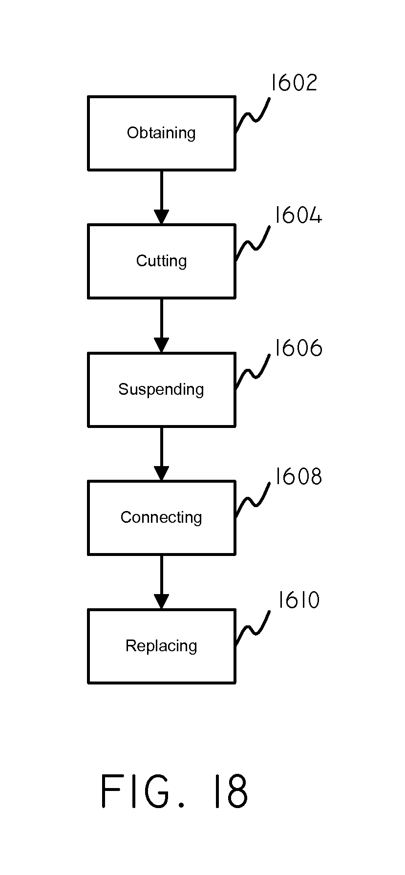
XML
uspto.report is an independent third-party trademark research tool that is not affiliated, endorsed, or sponsored by the United States Patent and Trademark Office (USPTO) or any other governmental organization. The information provided by uspto.report is based on publicly available data at the time of writing and is intended for informational purposes only.
While we strive to provide accurate and up-to-date information, we do not guarantee the accuracy, completeness, reliability, or suitability of the information displayed on this site. The use of this site is at your own risk. Any reliance you place on such information is therefore strictly at your own risk.
All official trademark data, including owner information, should be verified by visiting the official USPTO website at www.uspto.gov. This site is not intended to replace professional legal advice and should not be used as a substitute for consulting with a legal professional who is knowledgeable about trademark law.