Semiconductor-metal-on-insulator structures, methods of forming such structures, and semiconductor devices including such structures
Tang , et al.
U.S. patent number 10,325,926 [Application Number 15/464,060] was granted by the patent office on 2019-06-18 for semiconductor-metal-on-insulator structures, methods of forming such structures, and semiconductor devices including such structures. This patent grant is currently assigned to Micron Technology, Inc.. The grantee listed for this patent is Micron Technology, Inc.. Invention is credited to Andrew M. Bayless, Sanh D. Tang, John K. Zahurak, Ming Zhang.


View All Diagrams
| United States Patent | 10,325,926 |
| Tang , et al. | June 18, 2019 |
Semiconductor-metal-on-insulator structures, methods of forming such structures, and semiconductor devices including such structures
Abstract
Methods for fabricating semiconductor-metal-on-insulator (SMOI) structures include forming an acceptor wafer including an insulator material on a first semiconductor substrate, forming a donor wafer including a conductive material and an amorphous silicon material on a second semiconductor substrate, and bonding the amorphous silicon material of the donor wafer to the insulator material of the acceptor wafer. SMOI structures formed from such methods are also disclosed, as are semiconductor devices including such SMOI structures.
| Inventors: | Tang; Sanh D. (Kuna, ID), Zhang; Ming (Fremont, CA), Bayless; Andrew M. (Boise, ID), Zahurak; John K. (Eagle, ID) | ||||||||||
|---|---|---|---|---|---|---|---|---|---|---|---|
| Applicant: |
|
||||||||||
| Assignee: | Micron Technology, Inc. (Boise,
ID) |
||||||||||
| Family ID: | 44530576 | ||||||||||
| Appl. No.: | 15/464,060 | ||||||||||
| Filed: | March 20, 2017 |
Prior Publication Data
| Document Identifier | Publication Date | |
|---|---|---|
| US 20170194351 A1 | Jul 6, 2017 | |
Related U.S. Patent Documents
| Application Number | Filing Date | Patent Number | Issue Date | ||
|---|---|---|---|---|---|
| 12715704 | Mar 2, 2010 | 9608119 | |||
| Current U.S. Class: | 1/1 |
| Current CPC Class: | H01L 29/16 (20130101); H01L 29/04 (20130101); H01L 27/12 (20130101); H01L 27/24 (20130101); H01L 29/78603 (20130101); H01L 21/30604 (20130101); H01L 27/1021 (20130101); H01L 21/02532 (20130101); H01L 29/78645 (20130101); H01L 21/76251 (20130101); H01L 29/7841 (20130101); H01L 29/78648 (20130101); H01L 21/84 (20130101); H01L 27/10802 (20130101); H01L 27/1203 (20130101); H01L 21/76254 (20130101); H01L 21/02592 (20130101); H01L 29/78642 (20130101) |
| Current International Class: | H01L 21/02 (20060101); H01L 21/762 (20060101); H01L 21/84 (20060101); H01L 27/12 (20060101); H01L 27/24 (20060101); H01L 29/04 (20060101); H01L 29/16 (20060101); H01L 29/786 (20060101); H01L 27/108 (20060101); H01L 27/102 (20060101); H01L 21/306 (20060101); H01L 29/78 (20060101) |
| Field of Search: | ;257/348,629,632,646 ;438/406 |
References Cited [Referenced By]
U.S. Patent Documents
| 3988771 | October 1976 | Krishna |
| 4487639 | December 1984 | Lam et al. |
| 5098861 | March 1992 | Blackstone |
| 5102821 | April 1992 | Moslehi |
| 5106776 | April 1992 | Shen et al. |
| 5260233 | November 1993 | Buti et al. |
| 5373184 | December 1994 | Moslehi |
| 5378316 | January 1995 | Franke et al. |
| 5412598 | May 1995 | Shulman |
| 5465249 | November 1995 | Cooper, Jr. et al. |
| 5471039 | November 1995 | Irwin, Jr. et al. |
| 5510630 | April 1996 | Argawal et al. |
| 5563084 | October 1996 | Ramm et al. |
| 5600160 | February 1997 | Hvistendahl |
| 5874760 | February 1999 | Burns |
| 5904507 | May 1999 | Thomas |
| 5909618 | June 1999 | Forbes et al. |
| 5920105 | July 1999 | Okamoto et al. |
| 5930640 | July 1999 | Kenney |
| 5936274 | August 1999 | Forbes et al. |
| 5963469 | October 1999 | Forbes |
| 6017778 | January 2000 | Pezzani |
| 6033957 | March 2000 | Burns, Jr. et al. |
| 6137128 | October 2000 | Holmes et al. |
| 6191476 | February 2001 | Takahashi et al. |
| 6225151 | May 2001 | Gardner et al. |
| 6225165 | May 2001 | Noble, Jr. et al. |
| 6229161 | May 2001 | Nemati et al. |
| 6245663 | June 2001 | Zhao et al. |
| 6255731 | July 2001 | Ohmi |
| 6274888 | August 2001 | Suzuki et al. |
| 6291836 | September 2001 | Kramer |
| 6294418 | September 2001 | Noble |
| 6303468 | October 2001 | Aspar et al. |
| 6335231 | January 2002 | Yamazaki et al. |
| 6335258 | January 2002 | Aspar et al. |
| 6352894 | March 2002 | Goebel et al. |
| 6355501 | March 2002 | Fung et al. |
| 6355520 | March 2002 | Park et al. |
| 6365488 | April 2002 | Liao |
| 6391658 | May 2002 | Gates et al. |
| 6492662 | December 2002 | Hsu et al. |
| 6525953 | February 2003 | Johnson |
| 6559471 | May 2003 | Finder et al. |
| 6576944 | June 2003 | Weis |
| 6593624 | July 2003 | Walker |
| 6600173 | July 2003 | Tiwari |
| 6627924 | September 2003 | Hsu et al. |
| 6649980 | November 2003 | Noguchi |
| 6653174 | November 2003 | Cho et al. |
| 6690038 | February 2004 | Cho et al. |
| 6690039 | February 2004 | Nemati et al. |
| 6713791 | March 2004 | Hsu et al. |
| 6713810 | March 2004 | Bhattacharyya |
| 6727529 | April 2004 | Nemati et al. |
| 6744094 | June 2004 | Forbes |
| 6756286 | June 2004 | Moriceau et al. |
| 6764774 | July 2004 | Grill et al. |
| 6768156 | July 2004 | Bhattacharyya |
| 6777745 | August 2004 | Hshieh et al. |
| 6809044 | October 2004 | Aspar et al. |
| 6812504 | November 2004 | Bhattacharyya |
| 6815781 | November 2004 | Vyvoda et al. |
| 6841813 | January 2005 | Walker et al. |
| 6845034 | January 2005 | Bhattacharyya |
| 6870202 | March 2005 | Oka |
| 6881994 | April 2005 | Lee et al. |
| 6882008 | April 2005 | Ohsawa |
| 6888199 | May 2005 | Nowak et al. |
| 6891205 | May 2005 | Cho et al. |
| 6906354 | June 2005 | Hsu et al. |
| 6914286 | July 2005 | Park |
| 6934209 | August 2005 | Marr |
| 6940748 | September 2005 | Nejad et al. |
| 6940761 | September 2005 | Forbes |
| 6946365 | September 2005 | Aspar et al. |
| 6953953 | October 2005 | Horch |
| 6958263 | October 2005 | Bhattacharyya |
| 6958513 | October 2005 | Wang |
| 6965129 | November 2005 | Horch et al. |
| 6992349 | January 2006 | Lee et al. |
| 6995456 | February 2006 | Nowak |
| 7015092 | March 2006 | Jaiprakash et al. |
| 7029956 | April 2006 | Hsu et al. |
| 7052941 | May 2006 | Lee |
| 7075146 | July 2006 | Forbes |
| 7081663 | July 2006 | Bulucea |
| 7115939 | October 2006 | Forbes |
| 7120048 | October 2006 | Forbes |
| 7129538 | October 2006 | Lee et al. |
| 7151024 | December 2006 | Forbes |
| 7157771 | January 2007 | Forbes |
| 7158401 | January 2007 | Bhattacharyya |
| RE39484 | February 2007 | Bruel |
| 7180135 | February 2007 | Ioannou |
| 7195959 | March 2007 | Plummer et al. |
| 7205185 | April 2007 | Dokumaci et al. |
| 7250628 | July 2007 | Bhattacharyya |
| 7250646 | July 2007 | Walker et al. |
| 7259415 | August 2007 | Forbes |
| 7268373 | September 2007 | Gupta et al. |
| 7271052 | September 2007 | Forbes |
| 7279740 | October 2007 | Bhattacharyya et al. |
| 7304327 | December 2007 | Nemati et al. |
| 7323380 | January 2008 | Forbes |
| 7326969 | February 2008 | Horch |
| 7338862 | March 2008 | Huo et al. |
| 7358120 | April 2008 | Furukawa et al. |
| 7359229 | April 2008 | Ferrant et al. |
| 7362609 | April 2008 | Harrison et al. |
| 7368352 | May 2008 | Kim et al. |
| 7378325 | May 2008 | Kaneko et al. |
| 7410867 | August 2008 | Forbes |
| 7415690 | August 2008 | Liang et al. |
| 7440310 | October 2008 | Bhattacharyya |
| 7458439 | November 2008 | Horch |
| 7476939 | January 2009 | Okhonin et al. |
| 7488627 | February 2009 | Nemati et al. |
| 7491608 | February 2009 | Forbes |
| 7518182 | April 2009 | Abbott et al. |
| 7525137 | April 2009 | Walker et al. |
| 7538000 | May 2009 | Dao |
| 7560336 | July 2009 | Abbott |
| 7579240 | August 2009 | Forbes |
| 7589995 | September 2009 | Tang et al. |
| 7592209 | September 2009 | Chang |
| 7615436 | November 2009 | Kouznetsov et al. |
| 7619917 | November 2009 | Nirschl et al. |
| 7629651 | December 2009 | Nakajima |
| 7663188 | February 2010 | Chung |
| 7736969 | June 2010 | Abbott et al. |
| 7786505 | August 2010 | Yang et al. |
| 7816728 | October 2010 | Ho et al. |
| 7825455 | November 2010 | Lee et al. |
| 7838360 | November 2010 | Forbes |
| 7851859 | December 2010 | Tak et al. |
| 7883962 | February 2011 | Noble |
| 7897440 | March 2011 | Horch |
| 7929343 | April 2011 | Tang |
| 8018058 | September 2011 | Lee |
| 8084316 | December 2011 | Huo et al. |
| 8102025 | January 2012 | Ozeki et al. |
| 8148780 | April 2012 | Tang et al. |
| 8476145 | July 2013 | Or-Bach et al. |
| 8501559 | August 2013 | Tang et al. |
| 8501581 | August 2013 | Tang et al. |
| 8507966 | August 2013 | Tang et al. |
| 8518812 | August 2013 | Mariani et al. |
| 8519431 | August 2013 | Nemati et al. |
| 8524543 | September 2013 | Tang |
| 8558220 | October 2013 | Schricker et al. |
| 8598621 | December 2013 | Tang |
| 8772848 | July 2014 | Zahurak |
| 9209187 | December 2015 | Mariani et al. |
| 9214389 | December 2015 | Righetti et al. |
| 9224738 | December 2015 | Zanderigo et al. |
| 2001/0002062 | May 2001 | Noble, Jr. et al. |
| 2001/0024841 | September 2001 | Manning |
| 2001/0026477 | October 2001 | Manning |
| 2001/0048119 | December 2001 | Mizuno et al. |
| 2002/0024152 | February 2002 | Momoi et al. |
| 2002/0028541 | March 2002 | Lee et al. |
| 2002/0070454 | June 2002 | Yasukawa |
| 2002/0079537 | June 2002 | Houston |
| 2002/0081753 | June 2002 | Gates et al. |
| 2002/0094619 | July 2002 | Mandelman et al. |
| 2002/0142582 | October 2002 | Chan et al. |
| 2002/0158254 | October 2002 | Hsu et al. |
| 2002/0163019 | November 2002 | Mohsen |
| 2002/0185684 | December 2002 | Campbell et al. |
| 2002/0190265 | December 2002 | Hsu et al. |
| 2002/0190298 | December 2002 | Alsmeier et al. |
| 2002/0195655 | December 2002 | Hshieh et al. |
| 2003/0006461 | January 2003 | Tezuka et al. |
| 2003/0102469 | June 2003 | Jones et al. |
| 2003/0164501 | September 2003 | Suzuki et al. |
| 2003/0186521 | October 2003 | Kub et al. |
| 2003/0211705 | November 2003 | Tong et al. |
| 2003/0223292 | December 2003 | Nejad et al. |
| 2003/0235710 | December 2003 | Grill et al. |
| 2004/0007717 | January 2004 | Yoo |
| 2004/0022105 | February 2004 | Ohsawa |
| 2004/0094758 | May 2004 | Usuda et al. |
| 2004/0097022 | May 2004 | Werkhoven |
| 2004/0130015 | July 2004 | Ogihara et al. |
| 2004/0159853 | August 2004 | Nemati et al. |
| 2004/0174734 | September 2004 | Forbes |
| 2004/0214379 | October 2004 | Lee et al. |
| 2004/0233761 | November 2004 | Schwabe et al. |
| 2004/0262635 | December 2004 | Lee |
| 2004/0262679 | December 2004 | Ohsawa |
| 2005/0001232 | January 2005 | Bhattacharyya |
| 2005/0023656 | February 2005 | Leedy |
| 2005/0037582 | February 2005 | Dennard et al. |
| 2005/0059252 | March 2005 | Dokumaci et al. |
| 2005/0062079 | March 2005 | Wu |
| 2005/0146955 | July 2005 | Kajiyama |
| 2005/0230356 | October 2005 | Empedocles et al. |
| 2005/0282318 | December 2005 | Dao |
| 2005/0282356 | December 2005 | Lee |
| 2006/0034116 | February 2006 | Lam et al. |
| 2006/0071074 | April 2006 | Konevecki et al. |
| 2006/0082004 | April 2006 | Parekh et al. |
| 2006/0083058 | April 2006 | Ohsawa |
| 2006/0099776 | May 2006 | Dupont |
| 2006/0124974 | June 2006 | Cabral et al. |
| 2006/0125011 | June 2006 | Chang |
| 2006/0197115 | September 2006 | Toda |
| 2006/0010056 | October 2006 | Huo et al. |
| 2006/0227601 | October 2006 | Bhattacharyya |
| 2006/0249770 | November 2006 | Huo et al. |
| 2007/0012945 | January 2007 | Sugizaki |
| 2007/0018166 | January 2007 | Atanackovic et al. |
| 2007/0018223 | January 2007 | Abbott |
| 2007/0023805 | February 2007 | Wells et al. |
| 2007/0023817 | February 2007 | Dao |
| 2007/0029607 | February 2007 | Kouznetzov |
| 2007/0045709 | March 2007 | Yang |
| 2007/0047364 | March 2007 | Chuang et al. |
| 2007/0051994 | March 2007 | Song |
| 2007/0057328 | March 2007 | Taniguchi et al. |
| 2007/0064342 | March 2007 | Nakamura |
| 2007/0121696 | March 2007 | Ishii |
| 2007/0077694 | April 2007 | Lee |
| 2007/0080385 | April 2007 | Kim et al. |
| 2007/0127289 | June 2007 | Lee |
| 2007/0178649 | August 2007 | Swift |
| 2007/0215954 | September 2007 | Mouli |
| 2007/0252175 | November 2007 | Tang et al. |
| 2007/0264771 | November 2007 | Ananthan et al. |
| 2008/0003774 | January 2008 | Baek |
| 2008/0003778 | January 2008 | Eyck |
| 2008/0041517 | February 2008 | Moriceau et al. |
| 2008/0124867 | May 2008 | Brown |
| 2008/0128802 | June 2008 | Huo et al. |
| 2008/0149984 | June 2008 | Chang et al. |
| 2008/0164528 | July 2008 | Cohen et al. |
| 2008/0200014 | August 2008 | Park |
| 2008/0211023 | September 2008 | Shino |
| 2008/0211061 | September 2008 | Atwater, Jr. |
| 2008/0233694 | September 2008 | Li |
| 2008/0237776 | October 2008 | Abbott |
| 2008/0246023 | October 2008 | Zeng et al. |
| 2008/0296712 | December 2008 | Feuillet |
| 2008/0299753 | December 2008 | Figura et al. |
| 2009/0003025 | January 2009 | Mokhleshi et al. |
| 2009/0010056 | January 2009 | Kuo et al. |
| 2009/0014813 | January 2009 | Chao et al. |
| 2009/0022003 | January 2009 | Song et al. |
| 2009/0026522 | January 2009 | Ananthan |
| 2009/0050948 | February 2009 | Ishikawa |
| 2009/0072341 | March 2009 | Liu et al. |
| 2009/0079030 | March 2009 | Cheng et al. |
| 2009/0108351 | April 2009 | Yang et al. |
| 2009/0129145 | May 2009 | Slesazeck |
| 2009/0140290 | June 2009 | Schulze et al. |
| 2009/0170261 | July 2009 | Lee |
| 2009/0173984 | July 2009 | Wang |
| 2009/0179262 | July 2009 | Holz |
| 2009/0189228 | July 2009 | Zhang et al. |
| 2009/0200536 | August 2009 | Van Schaijk et al. |
| 2009/0201723 | August 2009 | Okhonin et al. |
| 2009/0207681 | August 2009 | Juengling |
| 2009/0213648 | August 2009 | Siesazeck |
| 2009/0218656 | September 2009 | Gonzalez et al. |
| 2009/0242865 | October 2009 | Lung et al. |
| 2009/0246952 | October 2009 | Ishizaka et al. |
| 2009/0250738 | October 2009 | Dyer |
| 2009/0315084 | December 2009 | Cha et al. |
| 2010/0001271 | January 2010 | Fumitake |
| 2010/0006938 | January 2010 | Jang |
| 2010/0008139 | January 2010 | Bae |
| 2010/0044670 | February 2010 | Ling |
| 2010/0061145 | March 2010 | Weis |
| 2010/0197141 | August 2010 | Tu et al. |
| 2010/0200916 | August 2010 | Gossner et al. |
| 2010/0203695 | August 2010 | Oh et al. |
| 2010/0207180 | August 2010 | Lee |
| 2010/0248153 | September 2010 | Lee et al. |
| 2010/0277982 | November 2010 | Okhonin |
| 2011/0006377 | January 2011 | Lee et al. |
| 2011/0024791 | February 2011 | Schulze et al. |
| 2011/0121366 | May 2011 | Or-Bach |
| 2011/0156044 | June 2011 | Lee et al. |
| 2011/0163357 | July 2011 | Tan et al. |
| 2011/0215371 | September 2011 | Tang et al. |
| 2011/0215396 | September 2011 | Tang et al. |
| 2011/0215407 | September 2011 | Tang et al. |
| 2011/0215408 | September 2011 | Tang et al. |
| 2011/0215436 | September 2011 | Tang et al. |
| 2011/0223725 | September 2011 | Kang et al. |
| 2011/0223731 | September 2011 | Chung et al. |
| 2011/0309434 | December 2011 | Huang |
| 2012/0205736 | August 2012 | Housley et al. |
| 2012/0223369 | September 2012 | Gupta et al. |
| 2012/0223380 | September 2012 | Lee et al. |
| 2014/0008721 | January 2014 | Filippini et al. |
| 2014/0106554 | April 2014 | Pozzi et al. |
| 2016/0049404 | February 2016 | Mariani et al. |
| 101405849 | Apr 2009 | CN | |||
| 101621036 | Jan 2010 | CN | |||
| 1494288 | Jan 2005 | EP | |||
| 1918998 | May 2008 | EP | |||
| H02-275663 | Nov 1990 | JP | |||
| H04-064249 | Feb 1992 | JP | |||
| H04-186815 | Jul 1992 | JP | |||
| H04-283914 | Nov 1992 | JP | |||
| 06-104446 | Apr 1994 | JP | |||
| H08-088153 | Apr 1996 | JP | |||
| H10-150176 | Jun 1998 | JP | |||
| H11-103035 | Apr 1999 | JP | |||
| 2000-150905 | May 2000 | JP | |||
| 2003-030980 | Jan 2003 | JP | |||
| 2004-303398 | Oct 2004 | JP | |||
| 2005-136191 | May 2005 | JP | |||
| 2005-327766 | Nov 2005 | JP | |||
| 2007-511895 | May 2007 | JP | |||
| 2008-010503 | Jan 2008 | JP | |||
| 2009-531860 | Sep 2009 | JP | |||
| 2011-508979 | May 2011 | JP | |||
| 10-0663359 | Oct 2006 | KR | |||
| 10-0702014 | Nov 2006 | KR | |||
| 10-0821456 | Apr 2008 | KR | |||
| 2009-0040460 | Apr 2009 | KR | |||
| 2009-0054245 | May 2009 | KR | |||
| 10-2010-0070835 | Jun 2010 | KR | |||
| 200802866 | Jan 2008 | TW | |||
| WO 2007/123609 | Nov 2007 | WO | |||
| WO 2009/088889 | Jul 2009 | WO | |||
Other References
|
CN 201180011589.X Search Rept., dated Aug. 21, 2014, Micron Technology, Inc. cited by applicant . CN 201180011589.X Search Rept., dated Apr. 10, 2015, Micron Technology, Inc. cited by applicant . CN 201180011628.6 Search Rept., dated Jun. 25, 2014, Micron Technology, Inc. cited by applicant . CN 201180011628.6 Search Rept., dated Feb. 27, 2015, Micron Technology, Inc. cited by applicant . CN 201180011630.3 Search Rept., dated Jul. 7, 2014, Micron Technology, Inc. cited by applicant . EP 11751050 Supp Search Rept., dated Nov. 14, 2014, Micron Technology, Inc. cited by applicant . EP 11751053 Supp. Search Rept., dated Jun. 4, 2014, Micron Tehnology, Inc. cited by applicant . PCT/US2011/024354 IPRP, dated Sep. 4, 2012, Micron Technology, Inc. cited by applicant . PCT/US2011/024354 Search Rept., dated Sep. 29, 2011, Micron Technology, Inc. cited by applicant . PCT/US2011/024354 Writ. Opin., dated Sep. 29, 2011, Micron Technology, Inc. cited by applicant . PCT/US2011/024376 IPRP, dated Sep. 4, 2012, Micron Technology, Inc. cited by applicant . PCT/US2011/024376 Search Rept., dated Sep. 28, 2011, Micron Technology, Inc. cited by applicant . PCT/US2011/024376 Writ. Opin., dated Sep. 28, 2011, Micron Technology, Inc. cited by applicant . PCT/US2011/024387 IPRP, dated Sep. 4, 2012, Micron Technology, Inc. cited by applicant . PCT/US2011/024387 Search Rept., dated Sep. 21, 2011, Micron Technology, Inc. cited by applicant . PCT/US2011/024387 Writ. Opin., dated Sep. 21, 2011, Micron Technology, Inc. cited by applicant . PCT/US2012/021438 IPRP, dated Aug. 13, 2013, Micron Technology, Inc. cited by applicant . PCT/US2012/021438 Search Rept., dated Aug. 28, 2012, Micron Technology, Inc. cited by applicant . PCT/US2012/021438 Writ. Opin., dated Aug. 28, 2012, Micron Technology, Inc. cited by applicant . PCT/US2012/025109 IPRP, dated Sep. 10, 2013, Micron Technology, Inc. cited by applicant . PCT/US2012/025109 Search Rept., dated Sep. 20, 2012, Micron Technology, Inc. cited by applicant . PCT/US2012/025109 Writ. Opin., dated Sep. 20, 2012, Micron Technology, Inc. cited by applicant . PCT/US2012/025115 IPRP, dated Sep. 12, 2013, Micron Technology, Inc. cited by applicant . PCT/US2012/025115 Search Rept., dated Oct. 4, 2012, Micron Technology, Inc. cited by applicant . PCT/US2012/025115 Writ. Opin., dated Oct. 4, 2012, Micron Technology, Inc. cited by applicant . TW 100106775 Search Report, dated Jun. 19, 2014, Micron Technology, Inc. cited by applicant . TW 100106776 Search Report, dated Nov. 25, 2014, Micron Technology, Inc. cited by applicant . TW 100106777 Search Report, dated Feb. 13, 2014, Applied Materials Inc. cited by applicant . TW 101104088 Search Report, dated Dec. 17, 2013, Micron Technology, Inc. cited by applicant . TW 101106601 SR Trans., dated Apr. 3, 2014, Micron Technology, Inc. cited by applicant . TW 101107759 SR Trans., dated Jun. 10, 2014, Micron Technology, Inc. cited by applicant . "IBM Builds World's Fastest Communications Microchip", Reuters U.S. Company News, Feb. 25, 2002, 1 p.; http://activequote300.fidelity.com/rtrnews/individual_n.../COMP&provider=- CBSMW%26toc_select%33Dmai. cited by applicant . Bae et al., "A Novel SiGe-Inserted SOI Structure for High Performance PDSOI CMOSFET", IEEE Electron Devices Meeting, 2000, pp. 667-670. cited by applicant . Belford et al., Performance-Augmented CMOS Using Back-End Uniaxial Strain, Device Research Conf. Digest, 2002, pp. 41-42. cited by applicant . Bhattacharyya, "The Role of Microelectronic Integration in Environmental Control: A Perspective", Materials Research Society Symposium Proceedings vol. 344, 1994, .pp. 281-293. cited by applicant . Burke et al., "Silicon Carbide Thyristors for Power Applications", 10th IEEE International Pulsed Power Conference Digest of Technical Papers vol. 1, 1995, United States, pp. 327-335. cited by applicant . Cheng et al., "SiGe-on-Insulator (SGOI): Substrate Preparation and MOSFET Fabrication for Electron Mobility Evaluation (and conference outline)", IEEE International SOI Conference, Oct. 2001, United States, pp. 13-14 and 3 page outline. cited by applicant . Cheong et al., "Investigation of Ultralow Leakage in MOS Capacitors on 4H SiC", IEEE Transactions on Electron Devices, vol. 51(9), Sep. 2004, United States, pp. 1361-1365. cited by applicant . Cho et al., "A Novel Capacitor-Less DRAM Cell Using Thin Capacitively-Coupled Thyristor (TCCT)", IEEE, 2005, U.S., 4 p. cited by applicant . Current et al., "Atomic-Layer Cleaving with SixGey Strain Layers for Fabrication of Si and Ge-Rich SOI Device Layers", IEEE International SOI Conference, Oct. 2001, U.S., p. 11-12. cited by applicant . Dimitraiadis et al., New a-SiC, Optically Controlled, Thyristor-Like Switch, Electronics Letters, vol. 28(17), Aug. 13, 1992, U.S.p. 1622-4. cited by applicant . Ernst et al., "Fabrication of a Novel Strained SiGe:C-channel Planar 55 nm nMOSFET for High-Performance CMOS", Digest of Technical Papers--Symposium on VLSI Tech., 2002, U.S., p. 92-93. cited by applicant . Feder, "I.B.M. Finds Way to Speed Up Chips", The New York Times, Jun. 8, 2001, 2 p.; http://www.nytimes.com/2001/06/08/technology/08BLUE.html. cited by applicant . Garone et al., "Mobility Enhancement and Quantum Mechanical Modeling in GexSi1-x Channel MOSFETs from 90 to 300K", IEEE Electron Devices Meeting, 1991, United States, pp. 29-32. cited by applicant . Gu et al., "High Performance Sub-100 nm Si Thin Film Transistors by Pattern Controlled Crystallization of Thin Channel Layer and High Temperature Annealing", Device Research Conference Digest, 2002, United States, pp. 49-50. cited by applicant . Hara et al., "High Performance Poly-Si TFTs on a Glass by a Stable Scanning CW Laser Lateral Crystallization", IEEE Electron Devices Meeting, 2001, United States, pp. 747-750. cited by applicant . Hara et al., Selective Single-Crystalline-Silicon Growth at the Pre-Defined Active Regions of TFTs on a Glass by a Scanning CW Layer Irradiation, IEEE Electron Devices Mtg, 2000, pp. 209-212. cited by applicant . Huang et al., "Carrier Mobility Enhancement in Strained Si-on-Insulator Fabricated by Wafer Bonding", Digest of Technical Papers--Symposium on VLSI Technology, 2001, U.S., pp. 57-58. cited by applicant . Jagar et al., "Single Grain Thin-Fim-Transistor (TFT) with SOI CMOS Performance Formed by Metal-Induced-Lateral-Crystallization", IEEE Electron Devices Meeting, 1999, U.S., pp. 293-296. cited by applicant . Jen et al.,Electrical and Luminescent Characteristics of a-SiC:H P-I-N Thin-Film LED's with Graded-Gap Junctions, IEEE Transactions on Electron Devices, vol. 44(4), Apr. 1997, U.S., p. 565-571. cited by applicant . Jeon et al., "A New Poly-Si TFT with Selectively Doped Channel Fabricated by Novel Excimer Laser Annealing", IEEE Electron Devices Meeting, 2000, United States, pp. 213-216. cited by applicant . Kesan et al., "High Performance 0.25 .mu.m p-MOSFETs with Silicon-Germanium Channels for 300K and 77K Operation", IEEE Electron Devices Meeting, 1991, United States, pp. 25-28. cited by applicant . Kim et al., "A New High-Performance Poly-Si TFT by Simple Excimer Laser Annealing on Selectively Floating a-Si Layer", IEEE Electron Devices Meeting, 2001; United States, pp. 751-754. cited by applicant . King et al, "A Low-Temperature (<550.degree. C.) Silicon-Germanium MOS Thin-Film Transistor Technology for Large-Area Electronics", IEEE Electron Devices Meeting, 1991, United States, pp. 567-570. cited by applicant . Kuriyama et al., "High Mobility Poly-Si TFT by a New Excimer Laser Annealing Method for Large Area Electronics", IEEE Electron Devices Meeting, 1991, United States, pp. 563-566. cited by applicant . Li et al., Design of High Speed Si/SiGe Heterojunction Complementary MOSFETs with Reduced Short-Channel Effects, Nat'l Central University; ChungLI, Taiwan, ROC, Aug. 2001, Contract No. NSC 89-2215-E-008-049, Nat'l Science Council of TW, p. 1, 9. cited by applicant . Lu et al., "A Buried-Trench DRAM Cell Using a Self Aligned Epitaxy Over Trench Technoloay", IEEE Electron Devices Meeting, 1988, United States, pp. 588-591. cited by applicant . Markoff, "I.B.M. Circuits are Now Faster and Reduce Use of Power", The New York Times, Feb. 25, 2002, reprinted Mar. 20, 2002, online http://story.news.yahoo.com/news?tmpl=story&u=/nyt/20020225/.../i_b_m_cir- cults_are_now_faster_and_reduce_use_of power, 1 page. cited by applicant . Mizuno et al., "High Performance CMOS Operation of Strained-SOI MOSFETs Using Thin Film SiGe-on-Insulator Substrate", Digest of Technical Papers--Symp. on VLSI Technology, 2002, pp. 106-107. cited by applicant . Myers et al., Deuterium Interactions in Oxygen-Implanted Copper, Jour. of Applied Physics; vol. 65(1), Jan. 1, 1989, pp. 311-321. cited by applicant . Nayfeh et al., "Electron Inversion Layer Mobility in Strained-Si n-Mosfet's with High Channel Doping Concentration Achieved by Ion Implantation", Device Research Conference Digest, 2002, United States, pp. 43-44. cited by applicant . Nemati et al., "A Novel High Density, Low Voltage SRAM Cell with a Vertical NDR Device", IEEE, 1998, United States, 2 pages. cited by applicant . Ono et al., "Analysis of Current-Voltage Characteristics in Polysilicon TFTs for LCDs", IEEE Electron Devices Meeting, 1988, United States, pp. 256-259. cited by applicant . Park et al., "Normal Incident SiGe/Si Multiple Quantum Well Infrared Detector", IEEE Electron Devices Meeting, 1991, United States, pp. 749-752. cited by applicant . Powell et al., "SiC Materials--Progress, Status, and Potential Roadblocks", Proceedings of the IEEE vol. 90(6), Jun. 2002, United States, pp. 942-955. cited by applicant . Rim et al., "Characteristics and Device Design of Sub-100 nm Strained SiN- and PMOSFETs", Digest of Technical Papers--Symposium on VLSI Technology, 2002, U.S., pp. 98-99. cited by applicant . Rim et al., "Strained Si NMOSFET's for High Performance CMOS Technology", Digest of Technical Papers--Symposium on VLSI Technology, 2001, United States, pp. 59-60. cited by applicant . Saggio et al., "Innovative Localized Lifetime Control in High-Speed IGBT's", IEEE Electron Device Letters vol. 18, No. 7, Jul. 1997, United States, pp. 333-335. cited by applicant . Sasago et al., "Cross-point phase change memory with 4F2 cell size driven by low-contact-resistivity 1 poly-Si diode", Digest of Tech. Papers--Symposium on VLSI Technology, 2009, pp. 24-25. cited by applicant . Shima et al., "<100> Channel Strained-SiGe p-MOSFET with Enhanced Hole Mobility and Lower Parasitic Resistance", Digest of Tech Papers--Symposium on VLSI Technology, 2002, pp. 94-95. cited by applicant . Sugizaki et al., "35-nm Gate-Length and Ultra Low voltage (0.45 V) Operation Bulk Thyristor-SRAMIDRAM (BT-RAM) Cell with Triple Selective Epitaxy Layers (TELs)", Digest of Technical Papers--Symposium on VLSI Technology, 2008, U.S., 1 p. (abstract). cited by applicant . Suliman et al., "Gate-Oxide Grown on the Sidewalls and Base of aU-Shaped Si Trench: Effects of the Oxide and Oxide/Si Interface Condition on the Properties of Vertical MOS Devices", Microelectronic Engineering vol. 72, 2004, Netherlands, pp. 247-252. cited by applicant . Takagi, Strained-Si- and SiGe-on-Insulator (Strained SOI and SGOI) MOSFETs for High Performance/Low Power CMOS Application, Device Research Conf.Digest, 2002, U.S., p. 37-40. cited by applicant . Tezuka et al., "High-Performance Strained Si-on-Insulator MOSFETs by Novel Fabrication Processes Utilizing Ge-Condensation Technique", Digest of Technical Papers--Symposium on VLSI Technology, 2002, U.S., pp. 96-97. cited by applicant . Tzeng et al., "Dry Etching of Silicon Materials in SF6 Based Plasmas", Journal of The Electrochemical Society vol. 134, Issue 9, 1987, pp. 2304-2309. cited by applicant . Van Meer et al., "Ultra-Thin Film Fully-Depleted SOI CMOS with Raised G/S/D Device Architecture for Sub-100 nm Applications", IEEE International SOI Conference, Oct. 2001, U.S., pp. 45-46. cited by applicant . Xie et al., "A Veritically Integrated Bipolar Storage Cell in 6H Silicon Carbide for Nonvolatile Memory Applications", IEEE Electron Device Letters vol. 15(6), Jun. 1994, U.S., pp. 212-214. cited by applicant . Yamada et al., "Spread Source/Drain (SSD) MOSFET Using Selective Silicon Growth for 64 Mbit DRAMs", IEEE Electron Devices Meeting, 1989, United States, pp. 35-38. cited by applicant . Yamauchi et al., "Drastically Improved Performance in Poly-Si TFTs with Channel Dimensions Comparable to Grain Size", IEEE Electron Devices Meeting, 1989, United States, pp. 353-356. cited by applicant . Yang et al., "High Performance CMOS Fabricated on Hybrid Substrate with Different Crystal Orientations", IEEE Electron Devices Meeting, 2003, United States, pp. 453-456. cited by applicant . Yu et al., "Low-Temperature Titanium-Based Wafer Bonding", Journal of the Electrocheical Society vol. 154, No. 1, 2007, United States, pp. H20-H25. cited by applicant. |
Primary Examiner: Malsawma; Lex H
Assistant Examiner: Jones; Eric W
Attorney, Agent or Firm: Wells St. John P.S.
Parent Case Text
CROSS-REFERENCE TO RELATED APPLICATIONS
The present application is a divisional of U.S. patent application Ser. No. 12/715,704 that was filed Mar. 2, 2010, which is related to co-pending U.S. patent application Ser. No. 12/715,843 filed on Mar. 2, 2010, and titled "FLOATING BODY CELL STRUCTURES, DEVICES INCLUDING SAME, AND METHODS FOR FORMING SAME"; co-pending U.S. patent application Ser. No. 12/715,743 filed on Mar. 2, 2010, and titled "SEMICONDUCTOR DEVICES INCLUDING A DIODE STRUCTURE OVER A CONDUCTIVE STRAP AND METHODS OF FORMING SUCH SEMICONDUCTOR DEVICES"; co-pending U.S. patent application Ser. No. 12/715,889 filed on Mar. 2, 2010, and titled "THYRISTOR-BASED MEMORY CELLS, DEVICES AND SYSTEMS INCLUDING THE SAME AND METHODS FOR FORMING THE SAME"; and co-pending U.S. patent application Ser. No. 12/715,922 filed on Mar. 2, 2010, and titled "SEMICONDUCTOR CELLS, ARRAYS, DEVICES AND SYSTEMS HAVING A BURIED CONDUCTIVE LINE AND METHODS FOR FORMING THE SAME", the disclosures of each of which are incorporated herein by reference.
Claims
What is claimed is:
1. A semiconductor-metal-on-insulator structure comprising: an insulator material on a first semiconductor substrate; an amorphous germanium material bonded to the insulator material; a conductive material over and in direct physical contact with the amorphous germanium material, the conductive material comprising one or more members of the group consisting of phase change material, titanium, titanium oxide, tantalum, tantalum oxide, tantalum nitride and tungsten oxide; and a second semiconductor substrate over the conductive material.
2. A semiconductor-metal-on-insulator structure comprising: an insulator material on a first semiconductor substrate; a conductive material over the insulator material, the conductive material comprising one or more members of the group consisting of phase change material and tungsten; an amorphous silicon material over the conductive material; and a second semiconductor substrate over the conductive material.
3. The semiconductor-metal-on-insulator structure of claim 2, further comprising a bonding material disposed between the conductive material and the amorphous silicon material.
4. The semiconductor-metal-on-insulator structure of claim 3, wherein the bonding material comprises at least one of an additional amorphous silicon material and an oxide material.
5. A semiconductor-metal-on-insulator structure comprising: an insulator material on a first semiconductor substrate; a conductive material over the insulator material; a first portion of an epitaxial silicon material and a second portion of a silicon-germanium material, the first and second portions being discrete portions and having an interface there between, the first portion or the second portion being bonded to the insulator material; and a second semiconductor substrate over the conductive material.
6. The semiconductor-metal-on-insulator structure of claim 5, wherein the insulator material comprises an oxide material having an amorphous silicon material formed thereon.
7. A method for fabricating a semiconductor-metal-on-insulator structure, comprising: forming an acceptor wafer comprising an insulator material formed over a first semiconductor substrate; forming a donor wafer comprising a conductive material over a precursor semiconductor substrate, an amorphous silicon material over the conductive material, and an implanted zone within the precursor semiconductor substrate, the conductive material comprising one or more members of the group consisting of phase change material, titanium, titanium oxide, tantalum, tantalum oxide, tantalum nitride and tungsten oxide; positioning the amorphous silicon material of the donor wafer in direct physical contact with the insulator material of the acceptor wafer and bonding the amorphous silicon material of the donor wafer to the insulator material of the acceptor wafer; and removing a portion of the precursor semiconductor substrate proximate the implanted zone within the precursor semiconductor substrate.
8. The method of claim 7, further comprising treating at least one of a surface of the amorphous silicon material and a surface of the insulator material with a chemical, a plasma, or an implant activation before bonding the amorphous silicon material of the donor wafer to the insulator material of the acceptor wafer.
9. The method of claim 7, wherein forming an acceptor wafer comprising an insulator material formed over a first semiconductor substrate comprises forming an oxide material over a first semiconductor substrate comprising crystalline silicon.
10. The method of claim 7, wherein forming a donor wafer comprising a conductive material over a precursor semiconductor substrate, an amorphous silicon material over the conductive material, and an implanted zone within the precursor semiconductor substrate comprises forming a conductive material over a crystalline silicon substrate, an amorphous silicon material over the conductive material, and a hydrogen-implanted zone within the crystalline silicon substrate.
11. The method of claim 7, wherein forming a donor wafer further comprises forming a dielectric material between the conductive material and the precursor semiconductor substrate.
12. The method of claim 7, wherein forming a donor wafer comprising a conductive material over a precursor semiconductor substrate comprises forming a non-reactive conductive material over the precursor semiconductor substrate and a reactive conductive material over the non-reactive conductive material and reacting the reactive conductive material with the amorphous silicon material of the donor wafer to form a conductive silicide material.
13. The method of claim 7, wherein forming the conductive material over the precursor semiconductor substrate comprises: depositing the conductive material over the precursor semiconductor substrate; forming a cap material over the conductive material; patterning the cap material and the conductive material; and forming a dielectric material between adjacent portions of the patterned cap material and patterned conductive material.
14. The method of claim 7, wherein forming the donor wafer further comprises forming at least one portion of an epitaxial silicon material and at least one portion of a silicon-germanium material between the conductive material and the amorphous silicon material.
15. The method of claim 7, wherein forming the donor wafer further comprises forming at least one portion of an oxide material and at least one portion of a nitride material between the conductive material and the amorphous silicon material.
16. A method of fabricating a semiconductor device, comprising: forming an acceptor wafer comprising an insulator material formed over a first semiconductor substrate; forming a donor wafer comprising a conductive material over a precursor semiconductor substrate, an amorphous silicon material over the conductive material, and an implanted zone within the precursor semiconductor substrate, the conductive material comprising one or more members of the group consisting of phase change material, titanium, titanium oxide, tantalum, tantalum oxide, tantalum nitride and tungsten oxide; positioning the amorphous silicon material of the donor wafer in direct physical contact with the insulator material of the acceptor wafer and bonding the amorphous silicon material of the donor wafer to the insulator material of the acceptor wafer; removing a portion of the precursor semiconductor substrate proximate the implanted zone to form a second semiconductor substrate; and fabricating at least one memory cell on the second semiconductor substrate.
17. The method of claim 16, further comprising patterning the conductive material to form at least one of a buried word line and a buried bit line.
18. The method of claim 16, wherein fabricating at least one memory cell on the second semiconductor substrate comprises: forming an active area from a portion of the second semiconductor substrate substantially surrounded on the sides and bottom by an additional insulator material; forming a high-k gate dielectric and a metal gate on the active area; and forming a source region and a drain region in the active area.
19. The method of claim 16, wherein fabricating at least one memory cell on the second semiconductor substrate comprises: etching the second semiconductor substrate to form at least one pillar; forming a source region, an active area, and a drain region in the at least one pillar; and forming a gate dielectric and a gate on the active area.
20. The method of claim 16, wherein fabricating at least one memory cell on the second semiconductor substrate comprises: forming a diode in the second semiconductor substrate; and forming a bottom electrode, a memory medium, and a top electrode on the diode.
Description
TECHNICAL FIELD
The present invention, in various embodiments, relates generally to semiconductor structures including a buried conductive material, and methods of forming such semiconductor structures. More specifically, embodiments of the present invention relate to a semiconductor-metal-on-insulator (SMOI) structure having a buried conductive material and methods of forming such structure. Additionally, the present invention relates to semiconductor devices including such SMOI structures and methods of forming such semiconductor devices.
BACKGROUND
One of the common trends in the electronics industry is the miniaturization of electronic devices. This is especially true for electronic devices operated through the use of semiconductor microchips. Microchips are commonly viewed as the brains of most electronic devices. In general, a microchip comprises a small silicon wafer upon which can be built millions or billions of nanoscopic electronic devices that are integrally configured to form electronic circuits. The circuits are interconnected in a unique way to perform a desired function.
With the desire to make high density microchips, it is necessary to decrease the size of the individual electronic devices and interconnects thereon. This movement also known as the so called "scale down" movement has increased the number and complexity of circuits on a single microchip.
Conventionally, electronic devices are formed side-by-side in a single plane on a common substrate, such as a silicon wafer. This side-by-side positioning, however, uses a relatively large amount of surface area, or "real estate," on the substrate. As a result, devices may be formed vertically in an effort to utilize less substrate area. In order to be competitive, such vertical devices are formed with high aspect ratios (i.e., the ratio of height to widths). However, as the aspect ratio of a device increases, it becomes increasingly difficult to satisfy both territory and electronic requirements of the corresponding interconnects. For this reason, simpler planar device scale downs dominate the industry in real practice to date.
A recent trend is to vertically stack semiconductor devices on a substrate. However, the stacking of semiconductor devices adds an additional complexity to connecting the components of the semiconductor device as well as providing efficient interconnects between the stacks.
Accordingly, there is a need for a method of forming a vertical semiconductor device which provides for competitive accessibility of interconnects to an electronic device in a stacked semiconductor device.
BRIEF DESCRIPTION OF THE DRAWINGS
FIGS. 1-6 are cross-sectional views of an SMOI structure during various processing acts in accordance with one embodiment of the disclosure;
FIGS. 7-10 are cross-sectional views of an SMOI structure during various processing acts in accordance with another embodiment of the disclosure;
FIGS. 11-14 are cross-sectional views of an SMOI structure during various processing acts in accordance with another embodiment of the disclosure;
FIGS. 15-18 are cross-sectional views of an SMOI structure during various processing acts in accordance with another embodiment of the disclosure;
FIGS. 19-21 are cross-sectional views of an SMOI structure during various processing acts in accordance with another embodiment of the disclosure;
FIGS. 22-28 are cross-sectional views of an SMOI structure during various processing acts in accordance with another embodiment of the disclosure;
FIGS. 29-31 are cross-sectional views of an SMOI structure during various processing acts in accordance with another embodiment of the disclosure;
FIGS. 32-34 are cross-sectional views of an SMOI structure during various processing acts in accordance with another embodiment of the disclosure;
FIGS. 35-38 are cross-sectional views of an SMOI structure during various processing acts in accordance with another embodiment of the disclosure;
FIG. 39 is a perspective view of one embodiment of a semiconductor device including an SMOI structure of the disclosure;
FIG. 40 is a perspective view of another embodiment of a semiconductor device including an SMOI structure of the disclosure;
FIG. 41 is a cross-sectional view of another embodiment of a semiconductor device including an SMOI structure of the disclosure;
FIG. 42 is a perspective view of another embodiment of a semiconductor device including an SMOI structure of the disclosure; and
FIG. 43 is a perspective view of another embodiment of a semiconductor device including an SMOI structure of the disclosure.
FIG. 44 is a schematic block diagram illustrating one embodiment of an electronic system that includes a semiconductor device including an SMOI structure of the disclosure.
DETAILED DESCRIPTION
A semiconductor-metal-on-insulator (SMOI) structure and methods of forming such an SMOI structure. Such structures include, in one embodiment, an insulator material on a first semiconductor substrate, an amorphous silicon material bonded to the insulator material, a conductive material over the amorphous silicon material, and a second semiconductor substrate over the conductive material. Methods of forming such structures include, in one embodiment, forming an acceptor wafer including an insulator material formed over a first semiconductor substrate, forming a donor wafer including forming a conductive material over a precursor semiconductor substrate, forming an amorphous silicon material over the conductive material, and implanting ions into the precursor semiconductor substrate at a depth to form an implanted zone. The amorphous silicon material of the donor wafer may be bonded to the insulator material of the acceptor wafer. A portion of the precursor semiconductor substrate above the implanted zone may then be removed.
The SMOI structures formed in accordance with the various embodiments of the disclosure include an amorphous silicon material bonded to an insulator material, a conductive material, or an additional amorphous silicon material. The amorphous silicon material exothermically crystallizes or reacts with the insulator material, the conductive material, or the additional amorphous silicon material, which allows for silicon atom rearrangement, which can improve the bond strength at the interface between the amorphous silicon material and the insulator material, the conductive material, or the additional silicon material. As such, the bond created between the amorphous silicon material and the at least one of the insulator material, the conductive material, and the additional amorphous silicon material may be substantially stronger than a bond created between two insulator materials, such as two oxide materials. Additionally, the bonding of the amorphous silicon material to the insulator material may occur at a relatively low temperature, such as at room temperature (from approximately 20.degree. C. to approximately 25.degree. C.), and, thus, reduces the risk of damage to any underlying devices formed on the first semiconductor substrate. Bonding of the amorphous silicon material to the at least one of the insulator material, the conductive material, and the additional amorphous silicon material is described in greater detail below. The SMOI structures formed in accordance with the various embodiments of the disclosure may also include a conductive material disposed between the insulator material and the second semiconductor substrate. The conductive material is buried beneath the second semiconductor substrate. The conductive material may be used, in some embodiments, to form an interconnect, such as a word line or a bit line, or to form a metal strap. Such an interconnect may be used to facilitate access to a semiconductor device formed in the second semiconductor substrate.
The SMOI structures formed in accordance with various embodiments of the disclosure may be used to fabricate a variety of semiconductor devices, such as an integrated circuit including a logic device formed in/on the first semiconductor substrate and a memory device formed in/on the second semiconductor substrate. Since the conductive material is buried beneath the second semiconductor substrate, devices formed on the second semiconductor substrate may be formed in relatively few process acts, as described in greater detail below. Additionally, the devices formed on/in the second semiconductor substrate may be self-aligned with the underlying interconnect and/or source and drain contacts, thus eliminating the need for a separate electrical contact. Furthermore, since a logic device may be formed on the first semiconductor substrate before the SMOI structure and the memory device are formed, the memory device is not exposed to the processing conditions used for the formation of the logic device. By forming such vertical, self-aligned, stacked integrated circuits, the cell size may be reduced, which provides for increased cache memory density.
The following description provides specific details, such as material types and processing conditions, in order to provide a thorough description of embodiments of the disclosure. However, a person of ordinary skill in the art will understand that embodiments of the present invention may be practiced without employing these specific details and in conjunction with conventional fabrication techniques. In addition, the description provided herein does not form a complete process flow for manufacturing a semiconductor device including the SMOI structure. Only those process acts and structures necessary to understand the embodiments of the disclosure are described in detail below. Additional acts to form a complete semiconductor device including the SMOI structure according to an embodiment of the invention may be performed by conventional techniques. In addition, it is understood that the methods described herein may be repeated as many times as desired to form multiple, stacked SMOI structures.
The materials described herein may be formed by any suitable technique including, but not limited to, spin coating, blanket coating, chemical vapor deposition ("CVD"), plasma enhanced chemical vapor deposition ("PECVD"), atomic layer deposition ("ALD"), plasma enhanced ALD, or physical vapor deposition ("PVD"). Alternatively, materials may be grown in situ. A technique suitable for depositing or growing a particular material may be selected by a person of ordinary skill in the art. While the materials described and illustrated herein may be formed as layers, the materials are not limited thereto and may be formed in other three-dimensional configurations.
In the following detailed description, reference is made to the accompanying drawings, which form a part hereof, and in which is shown, by way of illustration, specific embodiments in which the invention may be practiced. These embodiments are described in sufficient detail to enable a person of ordinary skill in the art to practice the invention. However, other embodiments may be utilized, and structural, logical, and electrical changes may be made without departing from the scope of the invention. The illustrations presented herein are not meant to be actual views of any particular system, logic device, memory cell, or semiconductor device, but are merely idealized representations which are employed to describe embodiments of the disclosure. The drawings presented herein are not necessarily drawn to scale. Additionally, elements common between drawings may retain the same numerical designation.
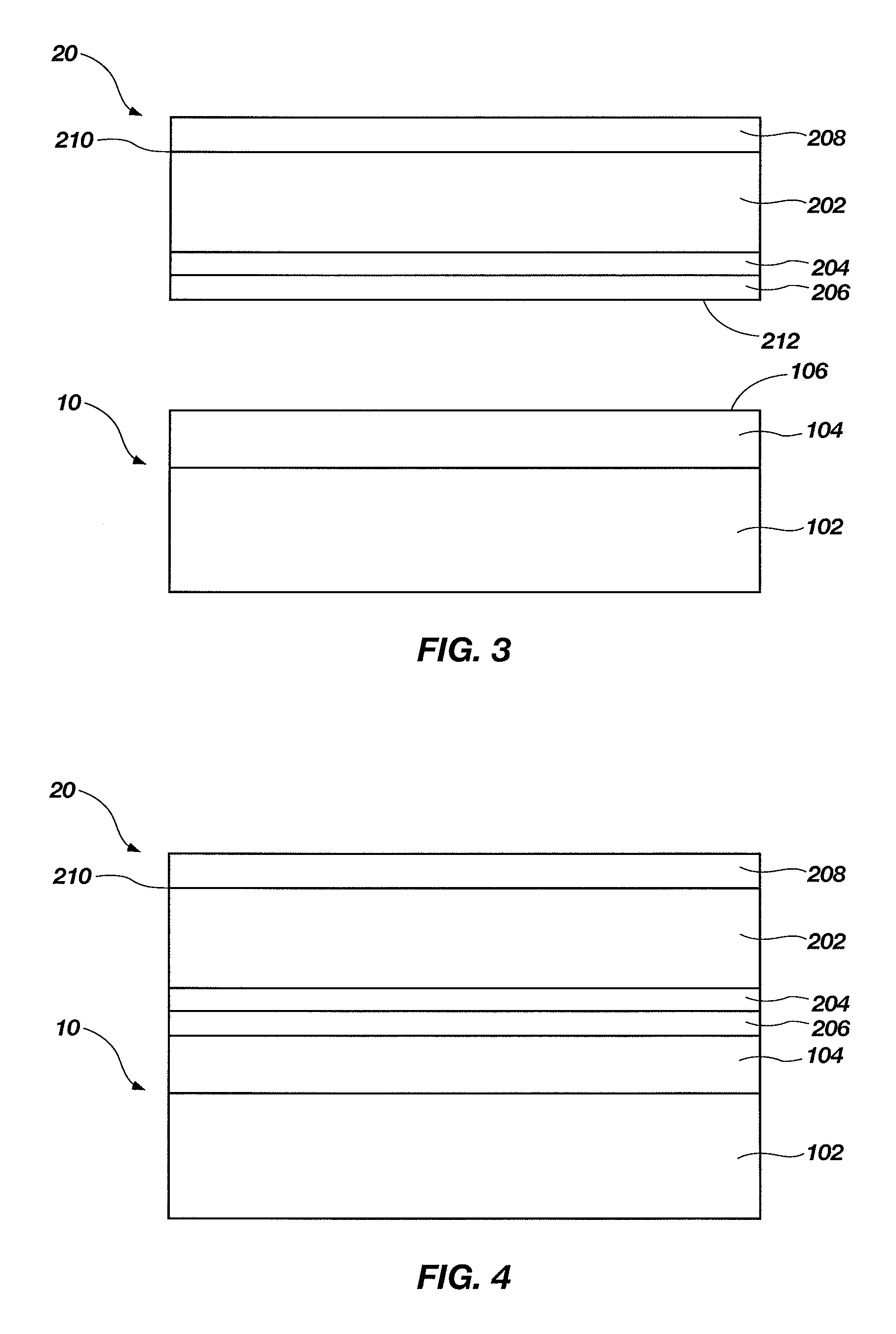
Referring now to the drawings, where like elements are designated by like reference numerals, FIGS. 1 through 6 are partial cross-sectional views of a method of forming an embodiment of an SMOI structure 30 (FIG. 6) including a conductive material 204, which is buried. The SMOI structure 30 is formed by bonding an acceptor wafer 10 (FIG. 1) and a donor wafer 20 (FIG. 2). FIG. 1 depicts the acceptor wafer 10. The acceptor wafer 10 may include a first semiconductor substrate 102 having an insulator material 104 formed thereon. The first semiconductor substrate 102 may include a fabrication substrate, such as a full or partial wafer of semiconductor material (e.g., silicon, gallium arsenide, indium phosphide, etc.), a full or partial silicon-metal-on-insulator (SMOI) type substrate, such as a silicon-on-glass (SOG), silicon-on-ceramic (SOC), or silicon-on-sapphire (SOS) substrate, or any other known, suitable fabrication substrate. As used herein, the term "wafer" includes conventional wafers as well as other bulk semiconductor substrates. The first semiconductor substrate 102 may be doped or undoped. An at least partially fabricated logic device (not shown), such as a CMOS device, may optionally be present on the first semiconductor substrate 102 and may be formed by conventional techniques. In one embodiment, the first semiconductor substrate 102 is bulk crystalline silicon.
The insulator material 104 may be a dielectric material including, by way of non-limiting example, silicon dioxide, borophosphosilicate glass (BPSG), borosilicate glass (BSG), phosphosilicate glass (PSG) or the like. In one embodiment, the insulator material 104 is a buried oxide. The insulator material 104 may be from about 500 .ANG. to about 2 .mu.m thick, such as from about 1000 .ANG. to about 2000 .ANG.. Techniques for deposition and in situ growth of such dielectric materials are known in the art and may include, for example, chemical vapor deposition (CVD), such as low pressure CVD or plasma enhanced CVD, atomic layer deposition (ALD), spin-on deposition, thermal decomposition, or thermal growth. The insulator material 104 includes an upper surface 106.
FIG. 2 is a partial cross-sectional view of one embodiment of the donor wafer 20 used to form the SMOI structure 30 (FIG. 6). The donor wafer 20 may include a precursor semiconductor substrate 202 having a conductive material 204 and an amorphous silicon material 206 formed thereon. In some embodiments, a polysilicon material or another amorphous material, such as amorphous germanium, may be substituted for the amorphous silicon material 206. The precursor semiconductor substrate 202 may be, for example, one of the fabrication substrates mentioned above for use as first semiconductor substrate 102. In one embodiment, the precursor semiconductor substrate 202 is a silicon substrate, such as a crystalline silicon substrate. The precursor semiconductor substrate 202 may be doped or undoped. The conductive material 204 may be a low resistivity material including, but not limited to, a phase change material, titanium, titanium silicide, titanium oxide, titanium nitride, tantalum, tantalum silicide, tantalum oxide, tantalum nitride, tungsten, tungsten silicide, tungsten oxide, tungsten nitride, other metal, metal silicide, metal oxide, or metal nitride materials, or combinations thereof, including multiple, different conductive materials. In one embodiment, the conductive material 204 may be formed from titanium nitride because titanium nitride has good adherence or adhesion to many materials, such as the material used as the precursor semiconductor substrate 202. Titanium nitride also has a high melting point (about 3000.degree. C.), which makes it unaffected by high processing temperatures. Titanium nitride also makes excellent ohmic contact with other conductive materials. Titanium nitride is also commonly used in semiconductor fabrication and, therefore, may easily be incorporated into conventional fabrication processes. In one embodiment, the conductive material 204 is a titanium-rich titanium nitride, such as metal mode titanium nitride (MMTiN). The conductive material 204 may also be formed from multiple conductive materials. In one embodiment, the conductive material 204 is a MMTiN material over the precursor semiconductor substrate 202 and a tungsten silicide material over the MMTiN material. In another embodiment, the conductive material 204 may be formed from a metal, such as titanium, tungsten or aluminum, with a layer of titanium material formed thereon. The thickness of the conductive material 204 may be optimized, depending on the material, to provide a low ohmic contact between the conductive material 204 and the precursor semiconductor substrate 202. For example, if the conductive material 204 is titanium nitride, such as MMTiN, the conductive material 204 may have a thickness of from about 10 nm to about 50 nm. The conductive material 204 may be formed by a deposition technique known in the art, such as, for example, atomic layer deposition (ALD), chemical vapor deposition (CVD), or plasma vapor deposition (PVD).
The amorphous silicon material 206 may be formed over the conductive material 204 by a deposition technique known in the art, such as, for example, ALD, CVD, or PVD. In one embodiment, the amorphous silicon material 206 may be formed on the conductive material 204 by PVD, followed by chemical mechanical planarization (CMP). The amorphous silicon material 206 may be of sufficient thickness to adhere to the insulator material 104 of the acceptor wafer 10 as described in greater detail below. For example, the thickness of the amorphous silicon material 206 may be from about 10 nm to about 50 nm. The amorphous silicon material 206 includes a surface 212.
As depicted in FIG. 2, the donor wafer 20 may also include a cleave portion 208 formed by implanting an atomic species into the precursor semiconductor substrate 202. The atomic species may be hydrogen ions, ions of rare gases, also termed inert or noble gases, or ions of fluorine. The atomic species may be implanted into the precursor semiconductor substrate 202 of the donor wafer 20 to form an implanted zone 210. The atomic species may be implanted into the precursor semiconductor substrate 202 prior to formation of the conductive material 204 thereon, after formation of the conductive material 204 thereon, or after formation of the amorphous silicon material 206 thereon. The implanted zone 210 may be formed at a desired depth in the precursor semiconductor substrate 202, which is dependent on parameters, such as implant dose and energy of the atomic species, as known in the art. The depth of the implanted zone 210 may correspond to the thickness of a second semiconductor substrate 202' of the SMOI structure 30 (FIG. 6). The implanted zone 210 may include microbubbles or microcavities including the implanted atomic species, which provide a weakened region within the precursor semiconductor substrate 202. The donor wafer 20 may be thermally treated at a temperature above that at which implantation is effected, but below the melting temperature of the conductive material 204, to effect crystalline rearrangement in the donor wafer 20 and coalescence of the microbubbles or microcavities. As described below, the donor wafer 20 may be cleaved at the implanted zone 210, forming the second semiconductor substrate 202' on the SMOI structure 30 (FIG. 6) and cleave portion 208. For clarity, the term "second semiconductor substrate" is used herein to refer to the semiconductor structure after removal of the cleave portion 208, while the term "precursor semiconductor substrate" is used herein to refer to the semiconductor structure before removal of the cleave portion 208.
As shown in FIGS. 3 and 4 the donor wafer 20 may be superposed onto the acceptor wafer 10 such that the amorphous silicon material 206 of the donor wafer 20 is in contact with the insulator material 104 of the acceptor wafer 10 (FIG. 4). The amorphous silicon material 206 of the donor wafer 20 may then be bonded to the insulator material 104 of the acceptor wafer 10 by exposure to heat. Prior to bonding the donor wafer 20 to the acceptor wafer 10, at least one of the surface 212 of the amorphous silicon material 206 and the upper surface 106 of the insulator material 104 may, optionally, be treated to improve the bond strength between the amorphous silicon material 206 and the insulator material 104. Such treatment techniques are known in the art and may include chemical, plasma, or implant activations. For example, the upper surface 106 of the insulator material 104 may be treated with a dilute ammonia hydroxide or hydrogen fluoride solution. The surface 212 of the amorphous silicon material 206 may also be exposed to a plasma of, for example, argon, to form a plasma-activated surface. Activating at least one of the surface 212 of the amorphous silicon material 206 and the upper surface 106 of the insulator material 104 may increase the kinetics of the subsequent bonding therebetween due to an increased mobility of ionic species (for example, hydrogen) created on the surface 212 of the amorphous silicon material 205 and the upper surface 106 of the insulator material 104.
As shown in FIG. 4, the amorphous silicon material 206 of the donor wafer 20 may be contacted and bonded with the insulator material 104 of the acceptor wafer 10 to form a precursor of the SMOI structure 30. The amorphous silicon material 206 may be bonded to the insulator material 104 by, for example, heating the SMOI structure 30 to a temperature of less than about 600.degree. C., such as from about 300.degree. C. to about 400.degree. C. If the insulator material 104 is formed from silicon dioxide, silicon-oxide bonds may form between the amorphous silicon material 206 and the insulator material 104. Because the conductive material 204 may be formed of a metal or other heat sensitive material, the temperature to which the SMOI structure 30 is exposed may be less than the melting point of the conductive material 204. The amorphous silicon material 206 and the insulator material 104 may also be bonded without heat, such as at ambient temperature (from about 20.degree. C. to about 25.degree. C.). Pressure may also be applied to the donor wafer 20 and the acceptor wafer 10 to bond the amorphous silicon material 206 to the insulator material 104. Once the donor wafer 20 is bonded to the acceptor wafer 10, the conductive material 204 from the donor wafer 20 may form a buried conductive material, which is disposed between the insulator material 104 and the precursor semiconductor substrate 202.
To form the SMOI structure 30 (FIG. 6), the cleave portion 208 may be removed from the precursor semiconductor substrate 202, as shown in FIG. 5. The cleave portion 208 may be removed by techniques known in the art, such as by applying a shear force to the implanted zone 210 or by applying heat or a jet gas stream at the implanted zone 210. The hydrogen or other ions implanted in the implanted zone 210 produce a weakened region in the precursor semiconductor substrate 202, which is susceptible to cleavage. The remaining portion of the second semiconductor substrate 202' may have a thickness, for example, of from about 50 nm to about 500 nm (from about 500 .ANG. to about 5000 .ANG.). A surface 302 of the SMOI structure 30, exposed after removing the cleave portion 208, may be rough and jagged. The exposed surface 302 of the SMOI structure 30 may be smoothed to a desired degree in order to facilitate further processing of the SMOI structure 30, as described below. The exposed surface 302 of the SMOI structure may be smoothed according to conventional techniques such as, for example, one or more of grinding, wet etching, chemical-mechanical polishing (CMP), and planar reactive ion etching (RIE).
The SMOI structure 30 and the other structures described below may be formed by modification of SMART-CUT.RTM. layer transfer technology. The SMART-CUT.RTM. layer transfer technology is described in detail in, for example, U.S. Pat. No. RE 39,484 to Bruel, U.S. Pat. No. 6,303,468 to Aspar et al., U.S. Pat. No. 6,335,258 to Aspar et al., U.S. Pat. No. 6,756,286 to Moriceau et al., U.S. Pat. No. 6,809,044 to Aspar et al., U.S. Pat. No. 6,946,365 to Aspar et al., and U.S. Patent Application Publication No. 2006/0099776 to Dupont. However, other processes suitable for manufacturing an SMOI substrate may also be used, if sufficiently low process temperatures are maintained. In conventional implementation of the SMART-CUT.RTM. layer transfer technology, donor wafers and acceptor wafers are bonded together using a high temperature anneal. The temperature used to bond the donor and acceptor wafers is from about 1000.degree. C. to about 1300.degree. C. However, due to the presence of the conductive material 204 in the SMOI structures described herein, the SMOI structures of the disclosure may, in some circumstances, be unable to withstand exposure to such temperatures without thermal damage. Accordingly, as described above, lower temperatures may be used to bond and acceptor wafer 10 and donor wafer 20.
FIG. 6 is an illustration of the SMOI structure 30 after the exposed surface 302 has been smoothed. Once the donor wafer 20 is bonded to the acceptor wafer 10 and the exposed surface 302 smoothed, then a semiconductor device, such as a memory cell, may be formed on and/or within the second semiconductor substrate 202' of the SMOI structure 30. As described below, the conductive material 204 of the SMOI structure 30 may function as, for example, an interconnect, such as a bit line or word line, as a gate, or as a metal strap.
FIGS. 7 through 10 are partial cross-sectional views of a method of forming an embodiment of an SMOI structure 50 (FIG. 10) including a conductive silicide material 410, which is buried. FIG. 7 illustrates an acceptor wafer 11 used to form the SMOI structure 50 (FIG. 10). The acceptor wafer 11 may be substantially similar to the acceptor wafer 10 described above and may be formed as described above regarding FIG. 1, with the exception that the amorphous silicon material 206 may be formed over the insulator material on the acceptor wafer 10. As shown in FIG. 7, the acceptor wafer 11 may include the amorphous silicon material 206 formed over the insulator material 104 and the insulator material 104 formed over the first semiconductor substrate 102.
FIG. 8 is a partial cross-sectional view of one embodiment of a donor wafer 40 used to form the SMOI structure 50 (FIG. 10). The donor wafer 40 may be substantially similar to the donor wafer 20 described above and may be formed as described above regarding FIG. 2, with the exception that the donor wafer 40 may include an optional non-reactive conductive material 402 and a reactive conductive material 404 instead of conductive material 204 (FIG. 2), and the amorphous silicon material 206 (FIG. 2) is not formed on the donor wafer 40. The non-reactive conductive material 402 may be formed of, for example, a metal nitride, such as titanium nitride. However, any conductive material that will not chemically react with the reactive conductive material 404 or a reaction product thereof may be used. The thickness of the non-reactive conductive material 402 may be relatively thin compared to the thickness of the reactive conductive material 404. For example, the non-reactive conductive material 402 may have a thickness of from about 20 .ANG. to about 200 .ANG.. The reactive conductive material 404 may be formed of a metal capable of reacting with the amorphous silicon material 206 or acts as a catalyst for crystallizing the amorphous silicon material 206. In one embodiment, the reactive conductive material 404 is titanium. The reactive conductive material 404 may have a thickness of from about 200 .ANG. to about 500 .ANG.. The non-reactive conductive material 402 and the reactive conductive material 404 may be formed by a deposition technique known in the art, such as, for example, ALD, CVD, or PVD.
As shown in FIG. 9, the donor wafer 40 may be superposed onto the acceptor wafer 11 and bonded thereto and the cleave portion 208 (FIG. 8) removed, as previously described regarding FIGS. 3-6. The resulting SMOI structure 50 may include the first semiconductor substrate 102, the insulator material 104, the amorphous silicon material 206, the reactive conductive material 404, the non-reactive conductive material 402, and the second semiconductor substrate 202'.
As shown in FIG. 10, the SMOI structure 50 may be annealed so that the reactive conductive material 404 chemically reacts with the amorphous silicon material 206, forming the conductive silicide material 410, which is buried beneath the non-reactive conductive material 402. The reactive conductive material 404 may be formed from titanium, which reacts with the amorphous silicon material 206 to form titanium silicide as the conductive silicide material 410. The reactive conductive material 404 and the non-reactive conductive material 402 may also be a single material, such as titanium-rich titanium nitride (MMTi). Excess titanium in the titanium-rich titanium nitride may react with the amorphous silicon material 206, forming the conductive silicide material 410. Annealing the SMOI structure 50 to form the conductive silicide material 410 may occur at a temperature of, for example, from about 600.degree. C. to about 800.degree. C. The bond strength between the conductive silicide material 410 and the insulator material 104 may be greater than that between the amorphous silicon material 206 and the insulator material 104. The conductive silicide material 410 may provide a lower resistance to the SMOI structure 50 than the reactive conductive material 404.
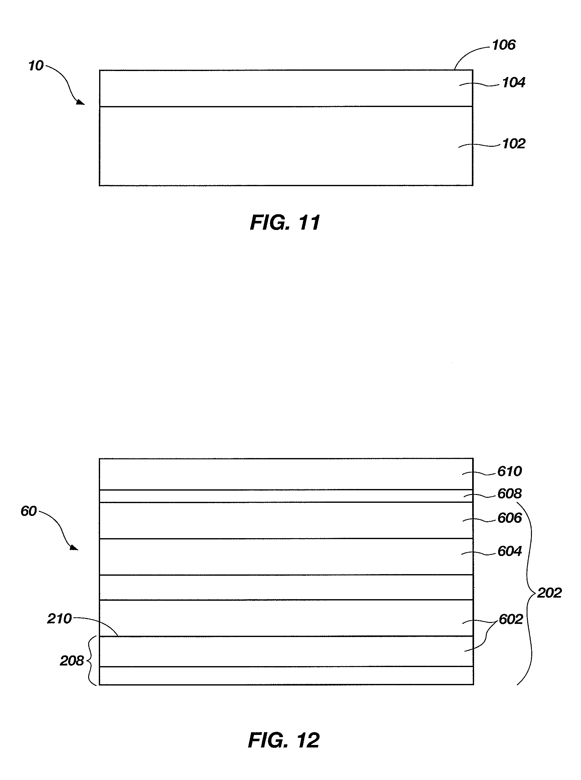
FIGS. 11 through 14 are partial cross-sectional views of a method of forming an embodiment of an SMOI structure 70 (FIG. 14) including a conductive material, which is buried beneath a doped semiconductor substrate. FIG. 11 illustrates an acceptor wafer 10, which is a substantial duplication of FIG. 1 and may be formed as described above regarding FIG. 1. As shown in FIG. 11, the acceptor wafer may include the insulator material 104 formed over the first semiconductor substrate 102.
FIG. 12 is a partial cross-sectional view of one embodiment of a donor wafer 60 used to form the SMOI structure 70 (FIG. 14). The donor wafer 60 may include a precursor semiconductive substrate 202 similar to the donor wafer 20 described above and may be formed as described above regarding FIG. 2. The precursor semiconductive substrate 202 may be doped and activated, as known in the art, to form a P+ doped region 602, an N- doped region 604, and an N+ doped region 606. In one embodiment, the precursor semiconductive substrate 202 may be doped using a high temperature process when the precursor semiconductive substrate does not yet include a MMTiN material 610 (FIG. 13) which may be damaged by such high temperature processes. In another embodiment, the P+ doped region 602 may be formed after the SMOI device 70 (FIG. 14) has been formed using a low temperature process for better dopant profile control. While FIG. 12 is depicted as including a particular order of the P+ doped region 602, the N- doped region 604, and the N+ doped region 606, it is understood that one of ordinary skill in the art may choose any combination of doped regions to achieve desired functions for the SMOI structure 70 (FIG. 14). Because the donor wafer 60 has two exposed surfaces from which the desired dopant may be implanted, the depth and concentration (i.e. highly doped or lightly doped) of the doped regions 602, 604, 606 may be more easily and accurately controlled than if the doped regions were formed after the donor wafer 60 is bonded to the acceptor wafer 10. As shown in FIG. 12, a silicide material 608 may be formed over the precursor semiconductor substrate 202, such as over the N+ doped region 606. The silicide material 608 may be formed by forming reactive conductive material over the precursor semiconductor substrate 202 so that the reactive conductive material reacts with the precursor semiconductor substrate 202 to form the silicide material 608. The silicide material 608 may have a low ohmic contact with the precursor semiconductor substrate 202. A metal mode titanium nitride (MMTiN) material may be formed over the silicide material 608. MMTiN material 610 and tungsten silicide material 612 may be formed by a deposition technique known in the art, such as, for example, ALD, CVD, or PVD. The thickness of the silicide material 608 may be relatively thin compared to the thickness of the MMTiN material 610. For example, the silicide material 608 may have a thickness of from about 50 .ANG. to about 500 .ANG.. The MMTiN material 610 may have a thickness of from about 500 .ANG. to about 1000 .ANG.. Also, as depicted in FIG. 12, the cleave portion 208 may be formed by implanting an atomic species into the precursor semiconductor substrate 202, forming the implanted zone 210 as previously described regarding FIG. 2. As shown in FIG. 12, the implanted zone 210 may be formed within the P+ doped region 602 of the precursor semiconductor substrate 202. The silicide material 608 and the MMTiN material 610 may have a substantially minimal impact on the implanting of the atomic species when forming the implanted zone 210
As shown in FIG. 13, a tungsten silicide material 612 and an amorphous silicon material 206 may be formed over the silicide material 608. The tungsten silicide material 612 may be formed by a deposition technique known in the art, such as, for example, ALD, CVD, or PVD. The tungsten silicide material 612 may be a better conductor than the MMTiN nitride material 610. In some embodiments, the tungsten silicide material 612 may be formed over the titanium silicide material 612 and MMTiN material 610 after the implanted zone 210 is formed.
As shown in FIG. 14, the donor wafer 60 may be superposed onto the acceptor wafer 10 and bonded thereto and the cleave portion 208 (FIG. 13) removed, as previously described regarding FIGS. 3-6. The resulting SMOI structure 70 may include the first semiconductor substrate 102, the insulator material 104, the amorphous silicon material 206, the tungsten silicide material 612, the MMTiN material 610, the silicide material 608, and the second semiconductor substrate 202' including the N+ doped region 606, the N- doped region 604, and the P+ doped region 602. In some embodiments, a second conductive material (not shown) may be formed over the P+ doped region 602 to form a top electrode which may be used to form a semiconductor device as described in greater detail below.
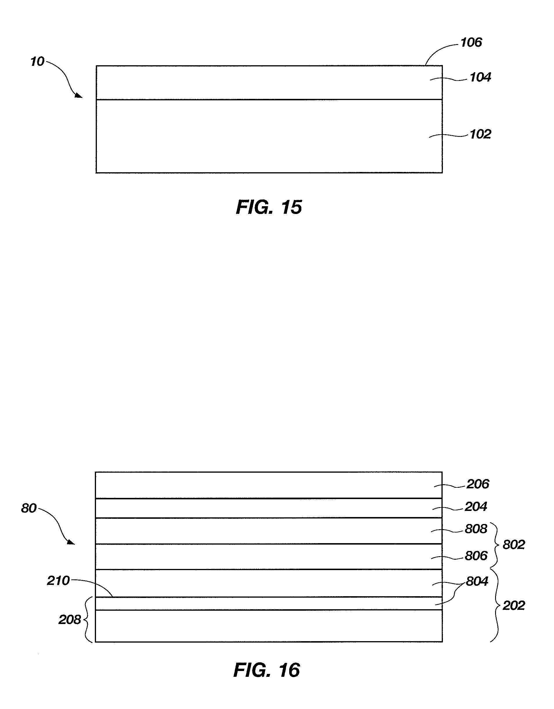
FIGS. 15 through 18 are partial cross-sectional views of another method of forming an embodiment of an SMOI structure 90 (FIG. 18) including a doped semiconductor material. FIG. 15 is a substantial duplication of FIG. 1 and may be formed as described above regarding FIG. 1. As shown in FIG. 15, the acceptor wafer 10 includes the insulator material 104 formed over the first semiconductor substrate 102.
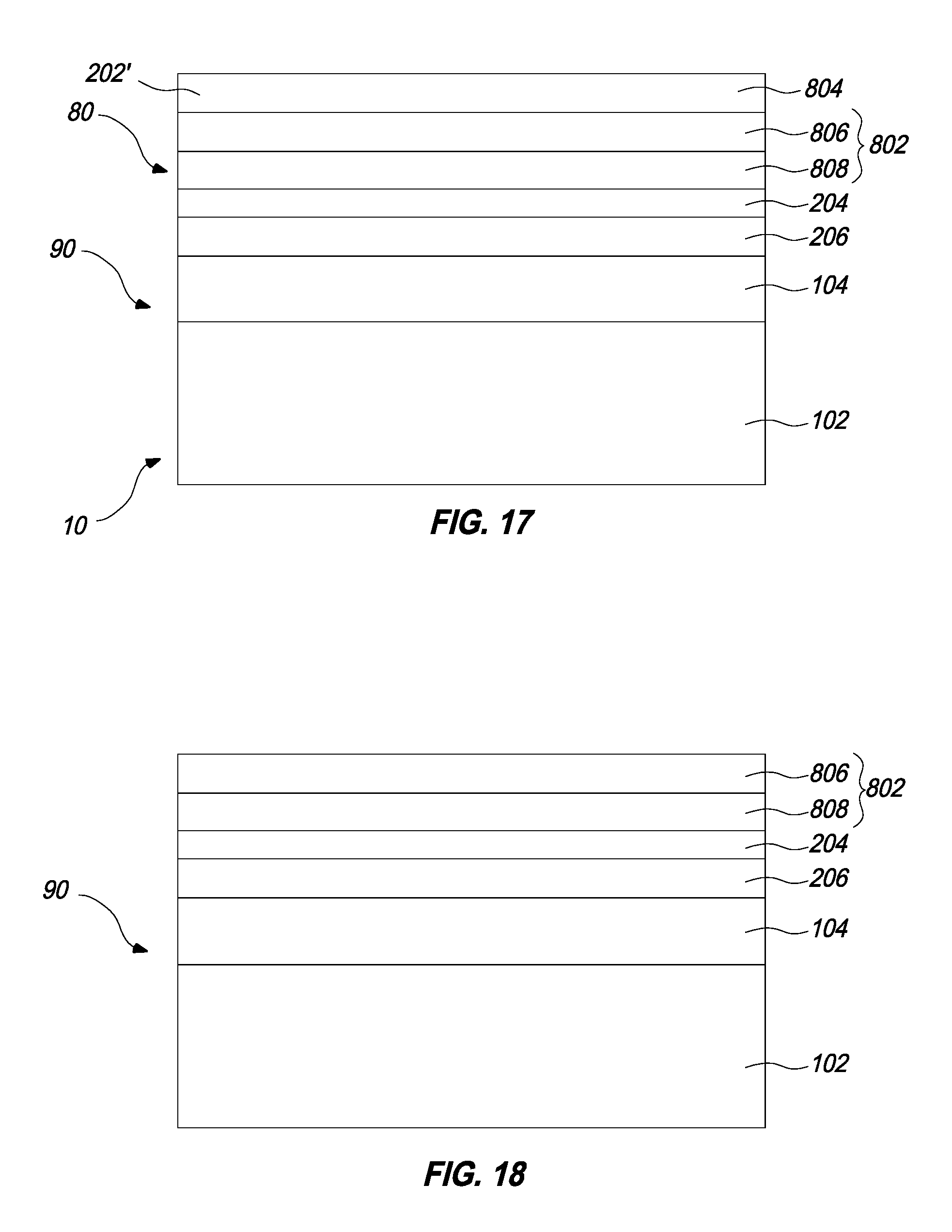
FIG. 16 is a partial cross-sectional view of one embodiment of a donor wafer 80 used to form the SMOI structure 90 (FIG. 18). The donor wafer 80 may be substantially similar to the donor wafer 20 described regarding FIG. 2 above and may be formed as described above regarding FIG. 2, with the exception that the donor wafer 80 may include a doped semiconductive material 802 disposed between the precursor semiconductor substrate 202 and the conductive material 204. The doped semiconductive material 802 may be formed of, for example, at least one of germanium (Ge), silicon carbide (SiC) and gallium nitride (GaN). The precursor semiconductor substrate 202 may be doped to form at least one P+ or N+ doped region 804. The doped semiconductive material 802 may also be doped to form a P doped region 806 and an N doped region 808. In one example, the P doped region 806 may include a P doped silicon carbide material adjacent the P+ or N+ doped region 804 of the precursor semiconductor substrate 202 and the N-doped region 808 may include an N doped silicon carbide material adjacent the P doped region 806. The doped semiconductive material 802 may be formed on the precursor semiconductor substrate 202 using conventional deposition or in situ growth techniques and may include, for example, chemical vapor deposition (CVD), such as low pressure CVD or plasma enhanced CVD, atomic layer deposition (ALD), spin-on deposition, thermal decomposition, or thermal growth. The conductive material 204 and the amorphous silicon material 206 may be deposited over the doped semiconductive material 802, and the precursor semiconductor substrate 202 may be implanted with an atomic species to form the implanted zone 210 and the cleave portion 208 as described above regarding FIG. 2.
As shown in FIG. 17, the donor wafer 80 may be superposed onto the acceptor wafer 10 and bonded thereto and the cleave portion 208 removed as previously described regarding FIGS. 3-6. The resulting SMOI structure 90 includes the first semiconductor substrate 102, the insulator material 104, the amorphous silicon material 206, the conductive material 204, the doped semiconductive material 802 including the N doped region 808 and the P doped region 806, and the second semiconductor substrate 202' including the P+ or N+ doped region 804. As shown in FIG. 18, the second semiconductor substrate 202' may be polished using techniques known in the art, such as CMP.
FIGS. 19 through 21 are partial cross-sectional views of another method of forming an embodiment of an SMOI structure 120 (FIG. 21) including the insulator material 104 and a high-k dielectric material 112. FIG. 19 is a substantial duplication of FIG. 1 and may be formed as described above regarding FIG. 1. As shown in FIG. 19, the acceptor wafer 10 includes the insulator material 104 formed over the first semiconductor substrate 102.
FIG. 20 is a partial cross-sectional view of one embodiment of a donor wafer 110 used to form the SMOI structure 120 (FIG. 21). The donor wafer 110 may be substantially similar to the donor wafer 20 described regarding FIG. 2 above and may be formed as described above regarding FIG. 2, with the exception that the donor wafer 110 includes a high-k dielectric material 112 disposed between the precursor semiconductor substrate 202 and the conductive material 204. The high-k dielectric material 112 may be formed of, for example, silicon dioxide, hafnium oxide, and other oxides, silicates, or aluminates of zirconium, aluminum, lanthanum, strontium, titanium, or combinations thereof including but not limited to Ta.sub.2O.sub.5, ZrO.sub.2, HfO.sub.2, TiO.sub.2, Al.sub.2O.sub.3, Y.sub.2O.sub.3, La.sub.2O.sub.3, HfSiO.sub.x, ZrSiO.sub.x, LaSiO.sub.x, YSiO.sub.x, ScSiO.sub.x, CeSiO.sub.x, HfLaSiO.sub.x, HfAlO.sub.x, ZrAlO.sub.x, and LaAlO.sub.x. In addition, multi-metallic oxides may be used, as may hafnium oxynitride, iridium oxynitride and other high-k dielectric materials in either single or composite layers. The high-k dielectric material 112 may be formed on the precursor semiconductor substrate 202 using conventional deposition or in situ growth techniques and may include, for example, chemical vapor deposition (CVD), such as low pressure CVD or plasma enhanced CVD, atomic layer deposition (ALD), spin-on deposition, thermal decomposition, or thermal growth. Optionally, the donor wafer 110 may also include a metal 113 and a doped region 115. The metal 113 may include, for example, a reactive conductor such as metal mode titanium (MMTi), titanium (Ti), tantalum (Ta), cobalt (Co), and nickel (Ni). The conductive material 204 and the amorphous silicon material 206 may be deposited over the high-k dielectric material 112 and the precursor semiconductor substrate 202 may be implanted with an atomic species to form the implanted zone 210 and the cleave portion 208 as described above regarding FIG. 2.
As shown in FIG. 21, the donor wafer 110 may be superposed onto the acceptor wafer 10 and bonded thereto and the cleave portion 208 (FIG. 20) removed as previously described regarding FIGS. 3-6. The resulting SMOI structure 120 includes the substrate 102, an insulator material 104, the amorphous silicon material 206, the conductive material 204, the high-k dielectric material 112 and the second semiconductor substrate 202'.
FIGS. 22 through 28 are cross-sectional views of a method of forming another embodiment of an SMOI structure 140 (FIG. 28) including a patterned conductive material 204'. FIG. 22 is a substantial duplication of FIG. 1 and may be formed as described above regarding FIG. 1. As shown in FIG. 22, the acceptor wafer 10 includes the insulator material 104 formed over the first semiconductor substrate 102.
FIG. 23 is a partial cross-sectional view of one embodiment of a donor wafer 130 used to form the SMOI structure 140 (FIG. 28). The donor wafer 130 includes the precursor semiconductor substrate 202 having the conductive material 204 and a cap material 132 formed thereon. The cap material 132 may be formed of a dielectric material, such as a nitride material or an oxide material. The cap material 132 may be formed by deposition techniques known in the art including, but not limited to, ALD, CVD, or PVD.
As shown in FIG. 24, the cap material 132 and the conductive material 204 may be patterned to form at least one structure 134 including the patterned cap material 132' and the patterned conductive material 204'. The cap material 132 and the conductive material 204 may be patterned using techniques known in the art, such as photoresist masking and anisotropic etching. Alternatively, in some embodiments, the patterned cap material 132' and the patterned conductive material 204' may be formed as at least one structure 134 using a damascene flow process, which is known in the art and is, therefore, not described in detail herein. As shown in FIG. 25, an interlevel dielectric material 136 may be deposited over the at least one structure 134 of the patterned cap material 132' and patterned conductive material 204'. The interlevel dielectric material 136 may be used to electrically isolate the at least one structure 134 from an adjacent structure 134. As shown in FIG. 26, the interlevel dielectric material 136 may be removed to expose an upper surface of the patterned cap material 132', such as by CMP, as known in the art. The patterned cap material 132' may act as a CMP stop.
As shown in FIG. 27, the amorphous silicon material 206 may be formed over the interlevel dielectric material 136 and the patterned cap material 132'. The donor wafer 130 may also be implanted with an atomic species forming the implanted zone 210 and the cleave portion 208 as previously described regarding FIG. 2. As shown in FIG. 28, the donor wafer 130 may be superposed onto the acceptor wafer 10 and bonded thereto and the cleave portion 208 removed as previously described regarding FIGS. 3-6. The resulting SMOI structure 140 includes the first semiconductor substrate 102, the insulator material 104, the amorphous silicon material 206, at least one structure 134 of the patterned cap material 132' and the conductive material 204', the at least one structure 134 being electrically isolated by the interlevel dielectric material 136, and the second semiconductor substrate 202'. Because the pillars 134 including the conductive material 204' are patterned and separated by the interlevel dielectric material 136, the conductive material 204' may be used as an interconnect, such as a word line or a bit line without further processing, as described in greater detail below.
In additional embodiments, the conductive material 204 may be formed on an acceptor wafer rather than a donor wafer. For example, FIGS. 29-31 illustrate partial cross-sectional views of another method of forming an embodiment of an SMOI structure 170 (FIG. 31) including the conductive material 204. As shown in FIG. 29, an acceptor wafer 150 includes the first semiconductor substrate 102, the insulator material 104, and the conductive material 204. The acceptor wafer 150 may, optionally, include a bonding material 152. The bonding material 152 (if present) may be either an amorphous silicon material, as previously described, or the bonding material 152 may be an oxide material, such as silicon dioxide. In some embodiments, the conductive material 204 may be patterned and filled with an interlevel dielectric material (not shown) as described above regarding FIGS. 22-28.
FIG. 30 is a partial cross-sectional view of one embodiment of a donor wafer 160 used to form the SMOI structure 170 (FIG. 31). The donor wafer 160 may include the precursor semiconductor substrate 202 and the amorphous silicon material 206. The donor wafer 160 may be implanted with an atomic species forming the implanted zone 210 and the cleave portion 208 as previously described regarding FIG. 2.
As shown in FIG. 31, the donor wafer 160 may be superposed onto the acceptor wafer 150 and bonded thereto, and the cleave portion 208 may be removed as previously described regarding FIGS. 3-6. The resulting SMOI structure 170 includes the first semiconductor substrate 102, the insulator material 104, the conductive material 204, the bonding material 152 (if present) bonded to the amorphous silicon material 206, and the second semiconductor substrate 202'.
In additional embodiments, multiple SMOI structures may be formed by creating multiple layers of silicon material on a donor wafer. For example, FIGS. 32-34 illustrate partial cross-sectional views of another method of forming an embodiment of an SMOI structure 200 (FIG. 32) including a conductive material 204. As shown in FIG. 32, an acceptor wafer 180 includes the first semiconductor substrate 102, the insulator material 104, and the conductive material 204.
FIG. 33 is a partial cross-sectional view of one embodiment of a donor wafer 190 used to form the SMOI structure 200 (FIG. 34). The donor wafer 190 may include the precursor semiconductor substrate 202, at least one portion of a silicon-germanium (SiGe) material 192, and at least one portion of an epitaxial (EPI) silicon material 194. The SiGe material 192 and EPI silicon material 194 may be formed by methods known in the art and at any desired thickness. Additionally, the SiGe material 192 and the EPI silicon material 194 may be doped or undoped. While FIG. 33 shows one portion of the SiGe material 192 and one portion of the EPI silicon material 194, multiple portions may be present by forming alternating portions of the SiGe material 192 and the EPI silicon material 194. In some embodiments, the amorphous silicon material 206, illustrated in dashed lines, may be optionally formed over the uppermost portion of the EPI silicon material 194 or the SiGe material 192. Alternatively, in some embodiments, the amorphous silicon material 206 may be omitted and the uppermost portion of the EPI silicon material 194 or the SiGe material 192 may be bonded to the acceptor wafer 180. The donor wafer 190 may also be implanted with an atomic species, forming the implanted zone 210 and the cleave portion 208 as previously described regarding FIG. 2.
As shown in FIG. 34, the donor wafer 190 may be superposed onto the acceptor wafer 180 and bonded thereto, and the cleave portion 208 may be removed as previously described regarding FIGS. 3-6. The resulting SMOI structure 200 includes the first semiconductor substrate 102, the insulator material 104, the conductive material 204, the amorphous silicon material 206 (if present), the at least one portion of the EPI silicon material 194, the at least one portion of the SiGe material 192, and the second semiconductor substrate 202'. While FIG. 33 is depicted as bonding the amorphous silicon material 206 to the conductive material 204, either of the EPI silicon material 194, the SiGe material 192, or the amorphous silicon material 206 (if present) may be used to bond the donor wafer 190 to the acceptor wafer 180. Once the SMOI structure 200 is formed, portions of the SiGe material 192 may be removed, such as, for example, utilizing a wet undercut etch. The portions of the SiGe material 192 that are removed may then be back filled with a dielectric material (not shown), such as an oxide material or the removed portions may be left unfilled, forming an air gap (not shown). Replacing portions of the SiGe material 192 with a dielectric material or an air gap may be used to form multiple SMOI structures on the substrate 102. In still further embodiments, the SMOI structure 200 may be formed without the conductive material 204, thus forming multiple SMOI structures on the substrate 102 without the conductive material 204.
In additional embodiments, the SMOI structure may be formed with a multi-portion buried dielectric material. For example, FIGS. 35-38 illustrate partial cross-sectional views of another method of forming an embodiment of an SMOI structure 250 (FIG. 38) including a multi-portion buried dielectric material. As shown in FIG. 35, an acceptor wafer 220 includes the first semiconductor substrate 102, the insulator material 104, at least one portion of an oxide material 222, and at least one portion of a nitride material 224. In some embodiments, the insulator material 104 may, optionally, be omitted. The oxide material 222 and the nitride material 224 may be formed in alternating portions. The oxide material 222 and the nitride material 224 may be formed by methods known in the art and at any desired thickness. While FIG. 35 is illustrated as including two portions of the oxide material 222 alternating with two portions of the nitride material 224, it is understood that any number of portions of oxide material 222 and nitride material 224 may be present.
FIG. 36 is a partial cross-sectional view of one embodiment of a donor wafer 230 used to form the SMOI structure 250 (FIG. 38). The donor wafer 230 may be substantially similar to the donor wafer 20 described above in FIG. 2 and may be formed as described above regarding FIG. 2. As shown in FIG. 36, the donor wafer 230 may include the precursor semiconductor substrate 202 and the amorphous silicon material 206. The donor wafer 230 may also be implanted with an atomic species forming the implanted zone 210 and the cleave portion 208.
As shown in FIG. 37, the donor wafer 230 may be superposed onto the acceptor wafer 220 and bonded thereto, and the cleave portion 208 may be removed as previously described regarding FIGS. 3-6. A resulting SMOI structure 240 includes the first semiconductor substrate 102, the insulator material 104, at least one portion of the oxide material 222, at least one portion of the nitride material 224, the amorphous silicon material 206, and the second semiconductor substrate 202'. While FIG. 37 is depicted as bonding the amorphous silicon material 206 to the at least one portion of the oxide material 222, any of the at least one portion of the nitride material 224, the at least one portion of the oxide material 222, or an additional amorphous silicon material (not shown) may be used to bond the donor wafer 230 to the acceptor wafer 220. Once the SMOI structure 240 is formed, portions of the nitride material 224 may be selectively removed, such as, for example, by a selective undercut utilizing a wet etch. The portions of the nitride material 224 that are removed may then be back filled with a conductive material 226, forming the SMOI structure 250 shown in FIG. 38. Replacing the nitride material 224 with the conductive material 226 may be used to form an SMOI structure 250 having multiple layers of the conductive material 226, which is buried. While the layers of the conductive material 226 are shown as having equal thicknesses, it is understood that different layers of the conductive material 226 may have varying thicknesses depending on the desired use of the SMOI structure 250. The multiple layers of the conductive material 226 may be used to form multiple interconnects, such as word lines and bit lines. In additional embodiments, when forming a semiconductor device on/in the second semiconductor substrate 202', only the uppermost portion of the conductive material 226 may be utilized to form a semiconductor device as described in greater detail below, and the lower portions of conductive material 226 may remain intact. The lower portions of conductive material 226 that remain intact may help improve the bond strength and stability of the SMOI structure 250.
The SMOI structures 30, 50, 70, 90, 120, 140, 170, 200, 250 described herein may be utilized to form numerous semiconductor devices as known in the art including those described in U.S. Pat. No. 7,589,995 to Tang et al. entitled One-transistor Memory Cell with Bias Gate, U.S. Patent Application Publication No. 2007/0264771 to Ananthan et al. entitled Dual Work Function Recessed Access Device and Methods of Forming, U.S. patent application Ser. No. 12/410,207 to Tang et al. entitled Methods, Devices, and Systems Relating to Memory Cells Having a Floating Body, U.S. patent application Ser. No. 12/419,658 to Tang entitled Methods, Devices, and Systems Relating to Memory Cells Having a Floating Body. The disclosure of each of the foregoing documents is incorporated herein in its entirety by this reference. The SMOI structures 30, 50, 70, 90, 120, 140, 170, 200, 250 may be used to form any semiconductor device with two or more terminals. For example, the SMOI structures 30, 50, 70, 90, 120, 140, 170, 200, 250 may be used to form dynamic random access memory (DRAM), resistive, non-volatile RAM (ReRAM), phase change RAM (PCRAM), one-time programmable read-only memory (OTP ROM), or cache memory devices.
FIG. 39 illustrates one example of an embodiment of a semiconductor device 300 including an SMOI structure 301 having a conductive material 304 buried beneath a second semiconductor substrate 312. The SMOI structure 301 may include, for example, a first semiconductor substrate 306, an insulator material 308, an amorphous silicon material 310, the conductive material 304, and the second semiconductor substrate 312. The SMOI structure 301 may be formed in a manner analogous to that described above in regard to FIG. 1-6, 7-10, 11-14, 15-18, 19-21, 22-28, 32-34, or 35-38.
The amorphous silicon material 310, the conductive material 304, and the second semiconductor substrate 312 may be patterned by conventional techniques in a first direction to form bit lines 314. Alternatively, if the SMOI structure 301 is formed in a manner analogous to that described above in regard to FIGS. 22-28, the conductive material 304 may already be patterned in the first direction. The second semiconductor substrate 312 may be patterned by conventional techniques in a second direction perpendicular to the first direction to form pillars 316 above the bit lines 314. The pillars 316 may be doped, as known in the art, to form a drain region 318, a source region 320, and a channel region 322. Alternatively, the second semiconductor substrate 312 may already be doped as previously described regarding FIGS. 11-14 and 15-18. Since the drain region 318, the source region 320, and the channel region 322 are formed vertically from the body of the pillars 316 and the pillar 316 is directly on top of the bit line 314, a higher device density may be achieved than with a conventional plan arrangement. A gate dielectric 324 may be formed on the sidewalls of the pillars 316 adjacent the channel regions 322. A gate 326 may also be formed on the sidewalls of the pillars 316 adjacent the gate dielectric 324. The gate dielectric 324 and the gate 326 may be formed using conventional techniques including conventional spacer etch techniques, which are not described in detail herein.
By utilizing the SMOI structure 301 to form the semiconductor device 300, the semiconductor device 300 may be formed in as few as three patterning acts. As previously described, the second semiconductor substrate 312 may be patterned in a first direction to form bit lines 314, the second semiconductor substrate 312 may be patterned in a second direction to form pillars 316 above the bit lines, and the gate 326 and the gate dielectric 324 may be patterned to form gate 326 and the gate dielectric 324 on the sidewalls of the pillars 316. Additionally, because the drain region 318, the source region 320, and the channel region 322 are formed from the pillar 316 above the bit line 314, no separate contact is needed to electrically connect the bit line 314 and the drain region 318. Furthermore, because a logic device (not shown) and back end of the line (BEOL) elements (not shown) may be formed on the first semiconductor substrate 306 prior to forming the semiconductor device 300, the semiconductor device 300 is not exposed to the processing conditions for forming the logic device and the BEOL elements. Avoiding exposure to such processing conditions may improve the reliability of the semiconductor device 300.
FIG. 40 illustrates another embodiment of a semiconductor device 400 including an SMOI structure 401 having a conductive material 403 buried beneath a second semiconductor substrate 412. The semiconductor device 400 may include a memory cell coupled to an access device, such as a diode 422. The SMOI structure 401 may include, for example, a first semiconductor substrate 406, a dielectric material 408, an amorphous silicon material 409, the conductive material 403, and the second semiconductor substrate 412. The SMOI structure 401 may be formed in a manner analogous to that described above in regard to FIG. 1-6, 7-10, 11-14, 15-18, 19-21, 22-28, 32-34, or 35-38.
The amorphous silicon material 409, the conductive material 403, and the second semiconductor substrate 412 may be patterned by conventional techniques in a first direction to form word lines 415. Alternatively, if the SMOI structure 401 is formed in a manner analogous to that described above in regard to FIGS. 22-28, the conductive material 403 may already be patterned in the first direction. A portion of the second semiconductor substrate 412 may be patterned in a second direction by conventional techniques to form a pillar 423. The second semiconductor substrate 412 may be doped by conventional techniques to form the diode 422 over the word lines 415. For example, the second semiconductor substrate 412 may be formed of a single crystalline silicon material and may be doped to form an N doped silicon material 414 and a P doped silicon material 416. The N doped silicon material 414 may include a portion of the second semiconductor substrate 412 extending over the word lines 415 which is not etched in the second direction. The P doped silicon material 416 may include the portion of the second semiconductor substrate 412 etched in the second direction to form the pillar 423. Alternatively, the second semiconductor substrate may already be doped as previously described regarding FIGS. 11-14 and 15-18. A bottom electrode 418 for the memory device 400 may be formed over the diode 412 using conventional techniques. For example, in one embodiment, the material of the bottom electrode 418 may be deposited over the second semiconductor substrate 412 prior to patterning the second semiconductor substrate 412. The material of the bottom electrode 418 may then be patterned and etched, using conventional techniques, simultaneously with the patterning and etching of the second semiconductor substrate 412. A memory medium 420, and a terminal electrode or bit line 424 may be formed over the diode 422 and in electrical communication therewith, using conventional techniques, which are not described in detail herein.
By utilizing the SMOI structure 401 to form the semiconductor device 400, the semiconductor device 400 may be formed in as few as three patterning acts. As previously described, the amorphous silicon material 409, the conductive material 403, and the second semiconductor substrate 412 may be patterned in a first direction to form word lines 415; the second semiconductor substrate 412 and the bottom electrode 418 may be patterned in a second direction to form the diode 422 and the bottom electrode 418; and the memory medium 420 and the bit line 424 may be patterned to form the memory medium 420 and the bit line 424 above the diodes 422. Because the memory medium 420 is one of the last materials to be deposited, phase change or resistant change materials may be used as the memory medium 420 since the memory medium 420 may not be exposed to, and altered by, high processing temperatures.
FIG. 41 illustrates another embodiment of a semiconductor device 500 including an SMOI structure 502 having a conductive material 504 buried beneath a second semiconductor substrate 514. The semiconductor device 500 may include a floating body memory cell 501 formed over and/or within the SMOI structure 502. The SMOI structure 502 may include, for example, a first semiconductor substrate 506, an insulator material 508, an amorphous silicon material 510, the conductive material 504, a high-k gate dielectric material 512, and the second semiconductor substrate 514. The SMOI structure 502 may be formed in a manner analogous to that described above in regard to FIGS. 29-31.
The floating body memory cell 501 includes an active region 516 surrounded on the sides by an additional insulator material 518. The active region 516 may be formed from the monocrystalline silicon of the second silicon substrate 514. The entire thickness of the second silicon substrate 514 may be used to form the floating body memory cell 501, the underlying high-k gate dielectric material 512 forming a back gate-dielectric and the conductive material 504 forming a metal back gate. Source and drain regions 526 may be formed by doping portions of the active region 516. The source and drain regions 526 will be doped differently than the active region 516. For example, the active region 516 may include P doped silicon while the source and drain regions 526 include N doped silicon.
As shown in FIG. 41, a second high-k material for a gate dielectric 520 is formed on the active region 516. The material for high-k gate dielectric 520 has a dielectric constant that is greater than that of silicon dioxide. Examples of a suitable material for high-k gate dielectric 520 include hafnium silicate, zirconium silicate, hafnium dioxide, or zirconium dioxide. A field-effect transistor (FET) gate 522 is formed on the high-k gate dielectric 520. The FET gate 522 and underlying high-k gate dielectric 520 may then be defined using conventional photolithographic techniques in combination with suitable etch processes, as known in the art. Spacers 524 may be formed flanking the sides of the FET gate 522 using conventional techniques, which are not described in detail herein.
By utilizing the SMOI structure 502 to form the semiconductor device 500, the floating body memory cell 501 may be formed in electrical communication with the conductive material 504, thus eliminating the need for an additional electrical contact between the floating body memory cell 501 and the conductive material 504. Additionally, because a logic device (not shown) and back end of the line (BEOL) elements (not shown) may be formed on the first semiconductor substrate 506 prior to forming floating body memory cell 501, the floating body memory cell 501 is not exposed to the processing conditions used to form the logic device and the BEOL elements. Avoiding exposure to such processing conditions may improve the reliability of the semiconductor device 500.
FIG. 42 illustrates another embodiment of a semiconductor device 600 including an SMOI structure 601 having a conductive material 603 buried beneath a second semiconductor substrate 614. The SMOI structure 601 may include, for example, a first semiconductor substrate 605, an insulator material 607, an amorphous silicon material 609, the conductive material 603, a dielectric material 611 and a second semiconductor substrate 614. The SMOI structure 601 may be formed in a manner analogous to that described above in regard to FIGS. 29-31.
The second semiconductor substrate 614 may be patterned and doped, as known in the art, to form a floating body region 616, a drain region 618 and a source region 619. The second semiconductor substrate 614 may be further patterned to form a recess in the floating body region 616 between the drain region 618 and the source region 619. A word line 620 may be formed in the recess. A dielectric material 622 may be formed between the word line 620 and the floating body region 616. The buried conductive material 603 acts as a buried gate for the memory cell. A contact 624 may be formed above the drain region 618 leading to a bit line 626. The contact 624 may comprise, for example, a N+ doped polysilicon plug or a metal plug. A common source 628 may be formed above the source region 619.
FIG. 43 illustrates a semiconductor device 700 including a plurality of the semiconductor devices 600 (FIG. 42). As illustrated in FIG. 43, the amorphous silicon material 609, the conductive material 603 and the dielectric material 611 may also be etched to form rows which are parallel to the bit lines 626. Similarly, in additional embodiments, the amorphous silicon material 609, the conductive material 603 and the dielectric material 611 may be etched to form rows (not shown) which are parallel to the bit lines 626.
By utilizing the SMOI structure 601 to form the semiconductor device 700, the floating body region 616 may be formed on top of the conductive material 603, thus eliminating the need for an additional electrical contact between the floating body region 616 and the conductive material 603. Additionally, because a logic device (not shown) and back end of the line (BEOL) elements (not shown) may be formed on the first semiconductor substrate 605 prior to forming floating body region 616, the floating body region 616 is not exposed to the processing conditions used for forming the logic device and the BEOL elements. Avoiding exposure of the floating body region 616 to such processing conditions may improve the reliability of the semiconductor device 600.
Semiconductor devices, such as those previously described herein, may be used in embodiments of electronic systems of the present invention. For example, FIG. 44 is a schematic block diagram of an illustrative electronic system 800 according to the present invention. The electronic system 800 may comprise, for example, a computer or computer hardware component, a server or other networking hardware component, a cellular telephone, a digital camera, a personal digital assistant (PDAs), portable media (e.g., music) player, etc. The electronic system 800 includes at least one memory device 801. The electronic system 800 further may include at least one electronic signal processor device 802 (often referred to as a "microprocessor"). At least one of the electronic signal processor device 802 and the at least one memory device 801 may comprise, for example, an embodiment of the semiconductor device 300, 400, 500, 600, 700 described above. In other words, at least one of the electronic signal processor device 802 and the at least one memory device 801 may comprise an embodiment of a semiconductor device including an SMOI structure having a buried conductive material as previously described in relation to the semiconductor devices 300, 400, 500, 600, 700 shown in FIGS. 39-43. The electronic system 800 may further include one or more input devices 804 for inputting information into the electronic system 800 by a user, such as, for example, a mouse or other pointing device, a keyboard, a touchpad, a button, or a control panel. The electronic system 800 may further include one or more output devices 806 for outputting information (e.g., visual or audio output) to a user such as, for example, a monitor, a display, a printer, an audio output jack, a speaker, etc. In some embodiments, the input device 804 and the output device 806 may comprise a single touchscreen device that can be used both to input information to the electronic system 800 and to output visual information to a user. The one or more input devices 804 and output devices 806 may communicate electrically with at least one of the memory device 801 and the electronic signal processor device 802.
CONCLUSION
In some embodiments, the present invention includes semiconductor-metal-on-insulator (SMOI) structures, devices including such structures and methods for forming such structures. The SMOI structures may include an insulator material on a first semiconductor substrate, an amorphous silicon material bonded to the insulator material, a conductive material over the amorphous silicon material and a second semiconductor substrate over the conductive material. A dielectric material may also be disposed between the conductive material and the second semiconductor substrate. In other embodiments, the conductive material may be patterned and adjacent portions of the patterned conductive material may be separated from one another by a dielectric material.
In additional embodiments, the present invention includes an SMOI that includes an insulator material on a first semiconductor substrate, an amorphous germanium material bonded to the insulator material, a conductive material over the amorphous germanium material and a second semiconductor substrate over the conductive material.
In additional embodiments, the present invention includes an SMOI structure that includes an insulator material on a first semiconductor substrate, a conductive material over the insulator material, at least one portion of an epitaxial silicon material and at least one portion of a silicon-germanium material, the at least one portion of the epitaxial silicon material or the at least one portion of the silicon-germanium material bonded to the insulator material, and a second semiconductor substrate over the conductive material. The insulator material may be formed of an oxide material having an amorphous silicon material formed thereon.
In additional embodiments, the present invention includes an SMOI structure including a first semiconductor substrate, at least one portion of an oxide material and at least one portion of a conductive material formed over the first semiconductor substrate, and a second semiconductor substrate formed over the conductive material.
In yet further embodiments, the present invention includes a semiconductor device that includes an insulator material on a first semiconductor substrate, an amorphous silicon material bonded to the insulator material, a conductive material over the amorphous silicon material, a second semiconductor substrate over the conductive material, and a memory cell on the second silicon substrate. The conductive material may form an interconnect. A logic device may also be formed on the first semiconductor substrate. In some embodiments, a dielectric material may be disposed between the conductive material and the second semiconductor substrate. The memory cell of the semiconductor device may include a floating body memory cell which includes an active area substantially physically isolated by an insulating material, a drain region and a source region formed within the active area, a high-k dielectric material formed on an active area between the drain region and the source region and a metal gate formed on the high-k dielectric.
In yet further embodiments, the present invention includes methods of forming an SMOI structure that include forming an acceptor wafer comprising an insulator material formed over a first semiconductor substrate, forming a donor wafer comprising a conductive material over a precursor semiconductor substrate, an amorphous silicon material over the conductive material, and an implanted zone within the precursor semiconductor substrate, bonding the amorphous silicon material of the donor wafer to the insulator material of the acceptor wafer, and removing a portion of the precursor semiconductor substrate proximate the implanted zone within the precursor semiconductor substrate. In some embodiments, at least one surface of the amorphous silicon material and a surface of the insulator material may be treated with a chemical, a plasma, or an implant activation before bonding the amorphous silicon material of the donor wafer to the insulator material.
In yet further embodiments, the present invention includes a method of fabricating a semiconductor device including forming an acceptor wafer comprising an insulator material formed over a first semiconductor substrate, forming a donor wafer comprising a conductive material over a precursor semiconductor substrate, an amorphous silicon material over the conductive material, and an implanted zone within the precursor semiconductor substrate, bonding the amorphous silicon material of the donor wafer to the insulator material of the acceptor wafer, removing a portion of the precursor semiconductor substrate proximate the implanted zone to form a second semiconductor substrate, and fabricating at least one memory cell on the second semiconductor substrate.
In yet further embodiments, the present invention includes methods of forming an SMOI structure that include forming an acceptor wafer comprising an insulator material formed over a first semiconductor substrate, forming a donor wafer comprising a conductive material over a precursor semiconductor substrate, an amorphous germanium material over the conductive material, and an implanted zone within the precursor semiconductor substrate, bonding the amorphous germanium material of the donor wafer to the insulator material of the acceptor wafer, and removing a portion of the precursor semiconductor substrate proximate the implanted zone within the precursor semiconductor substrate.
While the invention is susceptible to various modifications and alternative forms, specific embodiments have been shown by way of example in the drawings and have been described in detail herein. However, the invention is not intended to be limited to the particular forms disclosed. Rather, the invention is to cover all modifications, equivalents, and alternatives falling within the scope of the invention as defined by the following appended claims and their legal equivalents.
* * * * *
References
D00000
D00001
D00002
D00003
D00004
D00005
D00006
D00007
D00008
D00009
D00010
D00011
D00012

D00013

D00014
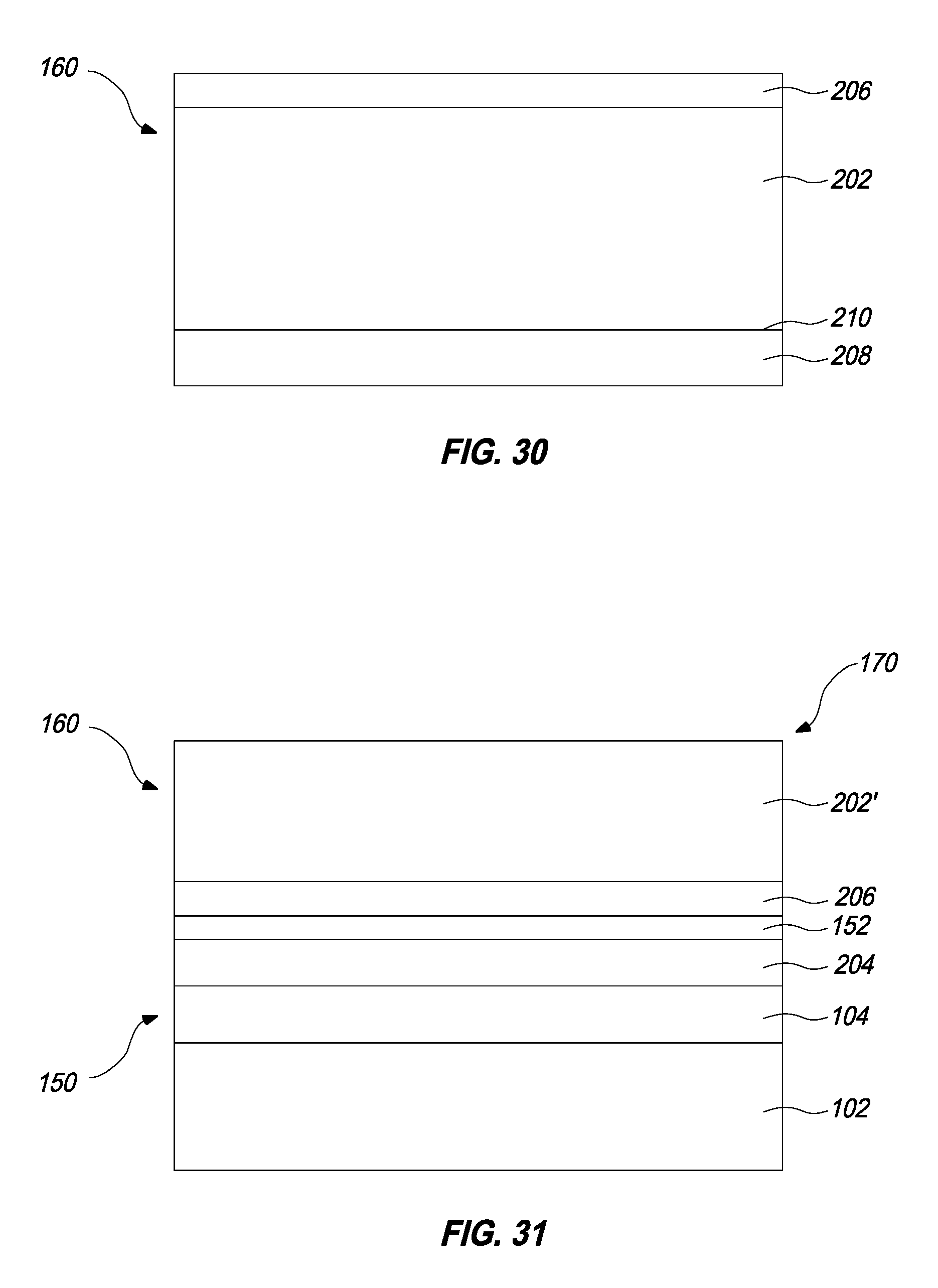
D00015

D00016
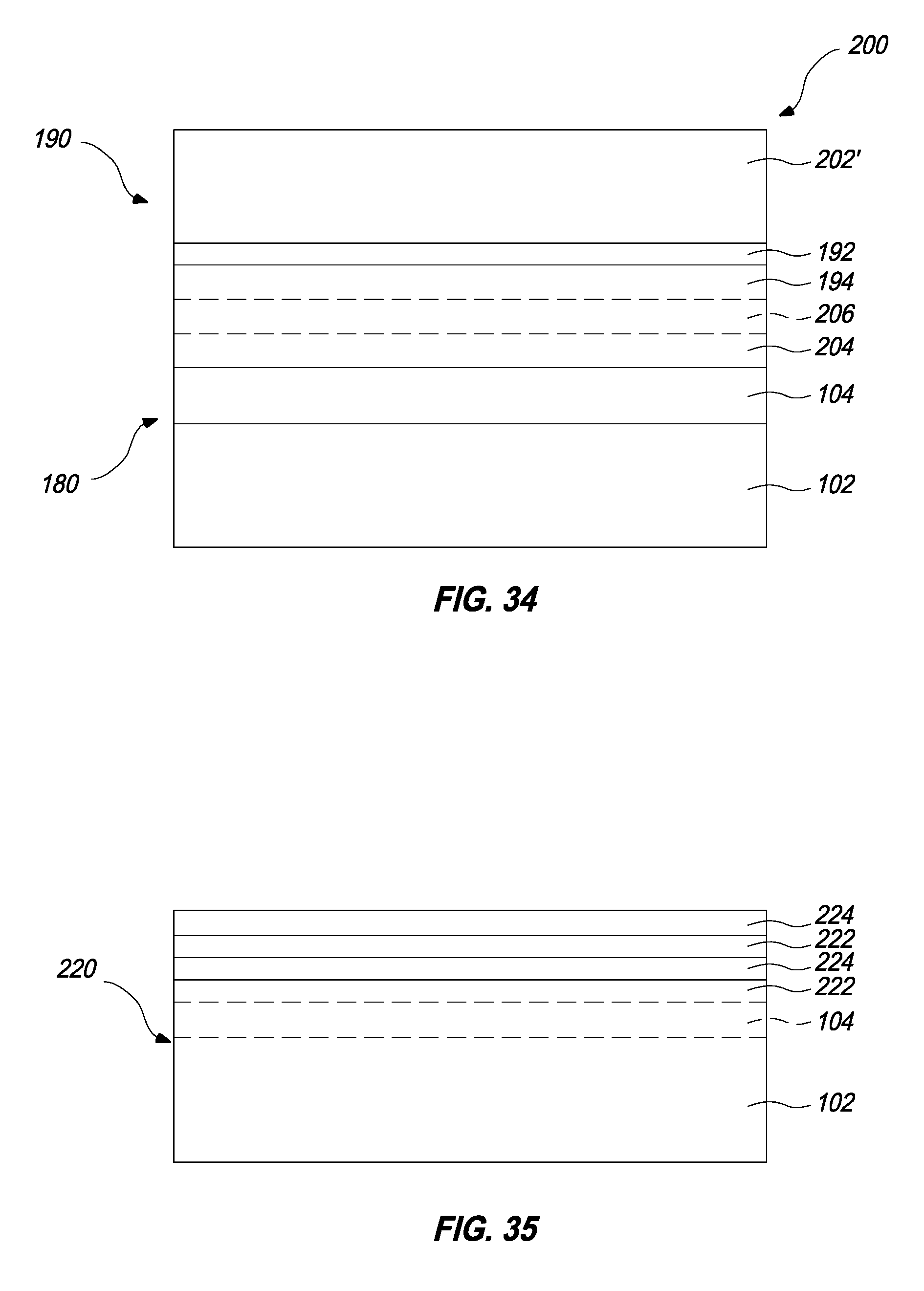
D00017

D00018

D00019

D00020

D00021

D00022

XML
uspto.report is an independent third-party trademark research tool that is not affiliated, endorsed, or sponsored by the United States Patent and Trademark Office (USPTO) or any other governmental organization. The information provided by uspto.report is based on publicly available data at the time of writing and is intended for informational purposes only.
While we strive to provide accurate and up-to-date information, we do not guarantee the accuracy, completeness, reliability, or suitability of the information displayed on this site. The use of this site is at your own risk. Any reliance you place on such information is therefore strictly at your own risk.
All official trademark data, including owner information, should be verified by visiting the official USPTO website at www.uspto.gov. This site is not intended to replace professional legal advice and should not be used as a substitute for consulting with a legal professional who is knowledgeable about trademark law.