Oxide-nitride-oxide stack having multiple oxynitride layers
Levy , et al. January 26, 2
U.S. patent number 10,903,068 [Application Number 15/099,025] was granted by the patent office on 2021-01-26 for oxide-nitride-oxide stack having multiple oxynitride layers. This patent grant is currently assigned to LONGITUDE FLASH MEMORY SOLUTIONS LTD.. The grantee listed for this patent is LONGITUDE FLASH MEMORY SOLUTIONS LTD.. Invention is credited to Sam G. Geha, Fredrick Jenne, Sagy Charel Levy, Krishnaswamy Ramkumar.


| United States Patent | 10,903,068 |
| Levy , et al. | January 26, 2021 |
Oxide-nitride-oxide stack having multiple oxynitride layers
Abstract
A semiconductor device including an oxide-nitride-oxide (ONO) structure having a multi-layer charge storing layer and methods of forming the same are provided. Generally, the method involves: (i) forming a first oxide layer of the ONO structure; (ii) forming a multi-layer charge storing layer comprising nitride on a surface of the first oxide layer; and (iii) forming a second oxide layer of the ONO structure on a surface of the multi-layer charge storing layer. Preferably, the charge storing layer comprises at least two silicon oxynitride layers having differing stochiometric compositions of Oxygen, Nitrogen and/or Silicon. More preferably, the ONO structure is part of a silicon-oxide-nitride-oxide-silicon (SONOS) structure and the semiconductor device is a SONOS memory transistor. Other embodiments are also disclosed.
| Inventors: | Levy; Sagy Charel (Zichron Yaakov, IL), Ramkumar; Krishnaswamy (San Jose, CA), Jenne; Fredrick (Mountain House, CA), Geha; Sam G. (Cupertino, CA) | ||||||||||
|---|---|---|---|---|---|---|---|---|---|---|---|
| Applicant: |
|
||||||||||
| Assignee: | LONGITUDE FLASH MEMORY SOLUTIONS
LTD. (Dublin, IE) |
||||||||||
| Appl. No.: | 15/099,025 | ||||||||||
| Filed: | April 14, 2016 |
Prior Publication Data
| Document Identifier | Publication Date | |
|---|---|---|
| US 20160300724 A1 | Oct 13, 2016 | |
Related U.S. Patent Documents
| Application Number | Filing Date | Patent Number | Issue Date | ||
|---|---|---|---|---|---|
| 13917500 | Jun 13, 2013 | 9355849 | |||
| 11811958 | Jun 13, 2007 | ||||
| 60931947 | May 25, 2007 | ||||
| Current U.S. Class: | 1/1 |
| Current CPC Class: | H01L 21/0214 (20130101); G11C 16/0466 (20130101); H01L 21/022 (20130101); H01L 27/11568 (20130101); H01L 29/518 (20130101); C23C 16/0272 (20130101); H01L 29/40117 (20190801); H01L 21/02148 (20130101); H01L 21/02271 (20130101); H01L 21/02211 (20130101); H01L 29/792 (20130101); C23C 16/308 (20130101); H01L 21/02164 (20130101); H01L 29/7833 (20130101); H01L 21/02238 (20130101); H01L 21/02255 (20130101) |
| Current International Class: | H01L 27/11573 (20170101); H01L 21/02 (20060101); H01L 21/28 (20060101); C23C 16/02 (20060101); H01L 29/792 (20060101); G11C 16/04 (20060101); H01L 21/314 (20060101); C23C 16/30 (20060101); H01L 29/51 (20060101); H01L 27/11568 (20170101); H01L 29/78 (20060101) |
References Cited [Referenced By]
U.S. Patent Documents
| 4257832 | March 1981 | Schwabe et al. |
| 4395438 | July 1983 | Chiang |
| 4490900 | January 1985 | Chiu |
| 4543707 | October 1985 | Ito et al. |
| 4667217 | May 1987 | Janning |
| 4843023 | June 1989 | Chiu et al. |
| 4870470 | September 1989 | Bass et al. |
| 5179038 | January 1993 | Kinney et al. |
| 5348903 | September 1994 | Pfiester et al. |
| 5404791 | April 1995 | Kervagoret |
| 5405791 | April 1995 | Ahmad et al. |
| 5408115 | April 1995 | Chang |
| 5464783 | November 1995 | Kim et al. |
| 5500816 | March 1996 | Kobayashi |
| 5543336 | August 1996 | Enami et al. |
| 5550078 | August 1996 | Sung |
| 5573963 | November 1996 | Sung |
| 5773343 | June 1998 | Lee et al. |
| 5793089 | August 1998 | Fulford et al. |
| 5817170 | October 1998 | Desu et al. |
| 5847411 | December 1998 | Morii |
| 5861347 | January 1999 | Maiti et al. |
| 5937323 | August 1999 | Orczyk et al. |
| 5939333 | August 1999 | Hurley et al. |
| 5972765 | October 1999 | Clark et al. |
| 5972804 | October 1999 | Tobin et al. |
| 6001713 | December 1999 | Ramsbey et al. |
| 6015739 | January 2000 | Gardner et al. |
| 6020606 | February 2000 | Liao |
| 6023093 | February 2000 | Gregor et al. |
| 6025267 | February 2000 | Pey et al. |
| 6074915 | June 2000 | Chen et al. |
| 6114734 | September 2000 | Eklund |
| 6127227 | October 2000 | Lin et al. |
| 6136654 | October 2000 | Kraft et al. |
| 6140187 | October 2000 | Debusk et al. |
| 6147014 | November 2000 | Lyding et al. |
| 6150286 | November 2000 | Sun et al. |
| 6153543 | November 2000 | Chesire et al. |
| 6157426 | December 2000 | Gu |
| 6162700 | December 2000 | Hwang et al. |
| 6174758 | January 2001 | Nachumovsky |
| 6174774 | January 2001 | Lee |
| 6214689 | April 2001 | Lim et al. |
| 6217658 | April 2001 | Orczyk et al. |
| 6218700 | April 2001 | Papadas |
| 6268299 | July 2001 | Jammy et al. |
| 6277683 | August 2001 | Pradeep et al. |
| 6287913 | September 2001 | Agnello et al. |
| 6297096 | October 2001 | Boaz |
| 6297173 | October 2001 | Tobin et al. |
| 6321134 | November 2001 | Henley et al. |
| 6335288 | January 2002 | Kwan et al. |
| 6348380 | February 2002 | Weimer et al. |
| 6365518 | April 2002 | Lee et al. |
| 6399484 | June 2002 | Yamasaki et al. |
| 6406960 | June 2002 | Hopper et al. |
| 6429081 | August 2002 | Doong et al. |
| 6433383 | August 2002 | Ramsbey et al. |
| 6440797 | August 2002 | Wu et al. |
| 6444521 | September 2002 | Chang et al. |
| 6445030 | September 2002 | Wu et al. |
| 6461899 | October 2002 | Kitakado et al. |
| 6462370 | October 2002 | Kuwazawa |
| 6468927 | October 2002 | Zhang et al. |
| 6469343 | October 2002 | Miura et al. |
| 6518113 | February 2003 | Buynoski |
| 6559026 | May 2003 | Rossman et al. |
| 6573149 | June 2003 | Kizilyalli et al. |
| 6586343 | July 2003 | Ho et al. |
| 6586349 | July 2003 | Jeon et al. |
| 6596590 | July 2003 | Miura et al. |
| 6599795 | July 2003 | Ogata |
| 6602771 | August 2003 | Inoue et al. |
| 6610614 | August 2003 | Niimi et al. |
| 6624090 | September 2003 | Yu et al. |
| 6661065 | December 2003 | Kunikiyo |
| 6670241 | December 2003 | Kamal et al. |
| 6677213 | January 2004 | Ramkumar et al. |
| 6709928 | March 2004 | Jenne et al. |
| 6713127 | March 2004 | Subramony et al. |
| 6717860 | April 2004 | Fujiwara |
| 6730566 | May 2004 | Niimi et al. |
| 6746968 | June 2004 | Tseng et al. |
| 6768160 | July 2004 | Li et al. |
| 6768856 | July 2004 | Akwani et al. |
| 6774433 | August 2004 | Lee et al. |
| 6787419 | September 2004 | Chen et al. |
| 6818558 | November 2004 | Rathor et al. |
| 6833582 | December 2004 | Mine et al. |
| 6835621 | December 2004 | Yoo et al. |
| 6867118 | March 2005 | Noro |
| 6884681 | April 2005 | Kamal et al. |
| 6903422 | June 2005 | Goda et al. |
| 6906390 | June 2005 | Nomoto et al. |
| 6912163 | June 2005 | Zheng et al. |
| 6913961 | July 2005 | Hwang |
| 6917072 | July 2005 | Noguchi et al. |
| 6946349 | September 2005 | Lee et al. |
| 6958511 | October 2005 | Halliyal |
| 7012299 | March 2006 | Mahajani et al. |
| 7015100 | March 2006 | Lee et al. |
| 7018868 | March 2006 | Yang et al. |
| 7033890 | April 2006 | Shone |
| 7033957 | April 2006 | Shiraiwa et al. |
| 7042054 | May 2006 | Ramkumar et al. |
| 7045424 | May 2006 | Kim et al. |
| 7060594 | June 2006 | Wang |
| 7084032 | August 2006 | Crivelli et al. |
| 7098154 | August 2006 | Yoneda |
| 7112486 | September 2006 | Cho et al. |
| 7115469 | October 2006 | Halliyal et al. |
| 7172940 | February 2007 | Chen et al. |
| 7189606 | March 2007 | Wang et al. |
| 7230294 | June 2007 | Lee et al. |
| 7238990 | July 2007 | Burnett et al. |
| 7250654 | July 2007 | Chen et al. |
| 7253046 | August 2007 | Higashi et al. |
| 7262457 | August 2007 | Hsu et al. |
| 7279740 | October 2007 | Bhattacharyya et al. |
| 7301185 | November 2007 | Chen et al. |
| 7312496 | December 2007 | Hazama |
| 7315474 | January 2008 | Lue |
| 7323742 | January 2008 | Georgescu |
| 7338869 | March 2008 | Fukada et al. |
| 7365389 | April 2008 | Jeon et al. |
| 7372113 | May 2008 | Tanaka et al. |
| 7390718 | June 2008 | Roizin et al. |
| 7410857 | August 2008 | Higashi et al. |
| 7425491 | September 2008 | Forbes |
| 7450423 | November 2008 | Lai et al. |
| 7463530 | December 2008 | Lue et al. |
| 7479425 | January 2009 | Ang et al. |
| 7482236 | January 2009 | Lee et al. |
| 7521751 | April 2009 | Fujiwara |
| 7535053 | May 2009 | Yamazaki |
| 7544565 | June 2009 | Kwak et al. |
| 7576386 | August 2009 | Lue et al. |
| 7588986 | September 2009 | Jung |
| 7601576 | October 2009 | Suzuki et al. |
| 7612403 | November 2009 | Bhattacharyya |
| 7636257 | December 2009 | Lue |
| 7642585 | January 2010 | Wang et al. |
| 7646041 | January 2010 | Chae et al. |
| 7646637 | January 2010 | Liao |
| 7670963 | March 2010 | Ramkumar et al. |
| 7688626 | March 2010 | Lue et al. |
| 7692246 | April 2010 | Dreeskornfeld et al. |
| 7713810 | May 2010 | Hagemeyer et al. |
| 7714379 | May 2010 | Lee |
| 7723789 | May 2010 | Lin et al. |
| 7737488 | June 2010 | Lai et al. |
| 7790516 | September 2010 | Willer et al. |
| 7811890 | October 2010 | Hsu et al. |
| 7879738 | February 2011 | Wang |
| 7910429 | March 2011 | Dong et al. |
| 7927951 | April 2011 | Kim et al. |
| 7948799 | May 2011 | Lue et al. |
| 7972930 | July 2011 | Jang et al. |
| 7999295 | August 2011 | Lai et al. |
| 8008713 | August 2011 | Dobuzinsky et al. |
| 8063434 | November 2011 | Polishchuk et al. |
| 8067284 | November 2011 | Levy |
| 8071453 | December 2011 | Ramkumar et al. |
| 8093128 | January 2012 | Koutny et al. |
| 8143129 | March 2012 | Ramkumar et al. |
| 8163660 | April 2012 | Puchner et al. |
| 8222688 | July 2012 | Jenne et al. |
| 8264028 | September 2012 | Lue et al. |
| 8283261 | October 2012 | Ramkumar |
| 8315095 | November 2012 | Lue et al. |
| 8318608 | November 2012 | Ramkumar et al. |
| 8482052 | July 2013 | Lue et al. |
| 8633537 | January 2014 | Polishchuk et al. |
| 8643124 | February 2014 | Levy et al. |
| 8710578 | April 2014 | Jenne et al. |
| 8859374 | October 2014 | Polishchuk et al. |
| 8860122 | October 2014 | Polishchuk et al. |
| 8940645 | January 2015 | Ramkumar et al. |
| 8993453 | March 2015 | Ramkumar et al. |
| 9093318 | July 2015 | Polishchuk et al. |
| 9306025 | April 2016 | Polishchuk et al. |
| 9349824 | May 2016 | Levy et al. |
| 9355849 | May 2016 | Levy et al. |
| 9449831 | September 2016 | Levy et al. |
| 9502543 | November 2016 | Polishchuk et al. |
| 9929240 | March 2018 | Polishchuk et al. |
| 10304968 | May 2019 | Ramkumar et al. |
| 10593812 | March 2020 | Ramkumar et al. |
| 2001/0052615 | December 2001 | Fujiwara |
| 2002/0020890 | February 2002 | Willer |
| 2002/0048200 | April 2002 | Kuwazawa |
| 2002/0048893 | April 2002 | Kizilyalli et al. |
| 2002/0109138 | August 2002 | Forbes |
| 2002/0141237 | October 2002 | Goda et al. |
| 2002/0154878 | October 2002 | Akwani et al. |
| 2003/0030100 | February 2003 | Lee et al. |
| 2003/0122204 | July 2003 | Nomoto et al. |
| 2003/0123307 | July 2003 | Lee et al. |
| 2003/0124873 | July 2003 | Xing et al. |
| 2003/0169629 | September 2003 | Goebel et al. |
| 2003/0183869 | October 2003 | Crivelli et al. |
| 2003/0222293 | December 2003 | Noro |
| 2003/0227049 | December 2003 | Sakakibara |
| 2003/0227056 | December 2003 | Wang et al. |
| 2004/0067619 | April 2004 | Niimi et al. |
| 2004/0071030 | April 2004 | Goda et al. |
| 2004/0094793 | May 2004 | Noguchi et al. |
| 2004/0104424 | June 2004 | Yamazaki |
| 2004/0129986 | July 2004 | Kobayashi et al. |
| 2004/0129988 | July 2004 | Rotondaro et al. |
| 2004/0173918 | September 2004 | Kamal et al. |
| 2004/0183091 | September 2004 | Hibino |
| 2004/0183122 | September 2004 | Mine et al. |
| 2004/0207002 | October 2004 | Ryu et al. |
| 2004/0227196 | November 2004 | Yoneda |
| 2004/0227198 | November 2004 | Mitani et al. |
| 2004/0251489 | December 2004 | Jeon et al. |
| 2005/0026637 | February 2005 | Fischer et al. |
| 2005/0056892 | March 2005 | Seliskar |
| 2005/0062098 | March 2005 | Mahajani et al. |
| 2005/0070126 | March 2005 | Senzaki |
| 2005/0079659 | April 2005 | Duan et al. |
| 2005/0088889 | April 2005 | Lee et al. |
| 2005/0093054 | May 2005 | Jung |
| 2005/0098839 | May 2005 | Lee et al. |
| 2005/0110064 | May 2005 | Duan et al. |
| 2005/0116279 | June 2005 | Koh |
| 2005/0141168 | June 2005 | Lee et al. |
| 2005/0186741 | August 2005 | Roizin et al. |
| 2005/0205920 | September 2005 | Jeon et al. |
| 2005/0224866 | October 2005 | Higashi et al. |
| 2005/0227501 | October 2005 | Tanabe et al. |
| 2005/0230766 | October 2005 | Nomoto et al. |
| 2005/0236679 | October 2005 | Hori et al. |
| 2005/0245034 | November 2005 | Fukuda et al. |
| 2005/0266637 | December 2005 | Wang |
| 2005/0275010 | December 2005 | Chen et al. |
| 2005/0275012 | December 2005 | Nara et al. |
| 2006/0008959 | January 2006 | Hagemeyer et al. |
| 2006/0017092 | January 2006 | Dong et al. |
| 2006/0022252 | February 2006 | Doh et al. |
| 2006/0051880 | March 2006 | Doczy et al. |
| 2006/0065919 | March 2006 | Fujiwara |
| 2006/0081331 | April 2006 | Campian |
| 2006/0111805 | May 2006 | Yokoyama et al. |
| 2006/0113586 | June 2006 | Wang |
| 2006/0113627 | June 2006 | Chen et al. |
| 2006/0131636 | June 2006 | Jeon et al. |
| 2006/0160303 | July 2006 | Ang et al. |
| 2006/0192248 | August 2006 | Wang |
| 2006/0202261 | September 2006 | Lue et al. |
| 2006/0202263 | September 2006 | Lee |
| 2006/0220106 | October 2006 | Choi et al. |
| 2006/0226490 | October 2006 | Burnett et al. |
| 2006/0228841 | October 2006 | Kim et al. |
| 2006/0228899 | October 2006 | Nansei et al. |
| 2006/0228907 | October 2006 | Cheng et al. |
| 2006/0237803 | October 2006 | Zhu et al. |
| 2006/0261401 | November 2006 | Bhattacharyya |
| 2006/0281331 | December 2006 | Wang |
| 2006/0284236 | December 2006 | Bhattacharyya |
| 2007/0012988 | January 2007 | Bhattacharyya |
| 2007/0022359 | January 2007 | Katoh et al. |
| 2007/0029625 | February 2007 | Lue et al. |
| 2007/0031999 | February 2007 | Ho et al. |
| 2007/0048916 | March 2007 | Suzuki et al. |
| 2007/0049048 | March 2007 | Rauf et al. |
| 2007/0051306 | March 2007 | Ivanov et al. |
| 2007/0066087 | March 2007 | Jung |
| 2007/0121380 | May 2007 | Thomas |
| 2007/0200168 | August 2007 | Ozawa et al. |
| 2007/0202708 | August 2007 | Luo |
| 2007/0210371 | August 2007 | Hisamoto et al. |
| 2007/0215940 | September 2007 | Ligon |
| 2007/0231991 | October 2007 | Willer et al. |
| 2007/0232007 | October 2007 | Forbes |
| 2007/0246753 | October 2007 | Chu et al. |
| 2007/0262451 | November 2007 | Rachmady et al. |
| 2007/0267687 | November 2007 | Lue |
| 2007/0268753 | November 2007 | Lue et al. |
| 2007/0272916 | November 2007 | Wang et al. |
| 2007/0272971 | November 2007 | Lee et al. |
| 2008/0009115 | January 2008 | Willer et al. |
| 2008/0029399 | February 2008 | Tomita et al. |
| 2008/0048237 | February 2008 | Iwata |
| 2008/0054346 | March 2008 | Saitoh et al. |
| 2008/0057644 | March 2008 | Kwak et al. |
| 2008/0087942 | April 2008 | Hsu et al. |
| 2008/0087946 | April 2008 | Hsu et al. |
| 2008/0121932 | May 2008 | Ranade |
| 2008/0135946 | June 2008 | Yan |
| 2008/0146042 | June 2008 | Kostamo et al. |
| 2008/0150003 | June 2008 | Chen et al. |
| 2008/0175053 | July 2008 | Lue et al. |
| 2008/0230853 | September 2008 | Jang et al. |
| 2008/0237684 | October 2008 | Specht et al. |
| 2008/0237694 | October 2008 | Specht et al. |
| 2008/0258203 | October 2008 | Happ et al. |
| 2008/0272424 | November 2008 | Kim et al. |
| 2008/0286927 | November 2008 | Kim et al. |
| 2008/0290398 | November 2008 | Polishchuk et al. |
| 2008/0290399 | November 2008 | Levy et al. |
| 2008/0290400 | November 2008 | Jenne et al. |
| 2008/0291726 | November 2008 | Lue et al. |
| 2008/0293207 | November 2008 | Koutny et al. |
| 2008/0293254 | November 2008 | Ramkumar et al. |
| 2008/0293255 | November 2008 | Ramkumar |
| 2008/0296664 | December 2008 | Ramkumar et al. |
| 2009/0011609 | January 2009 | Ramkumar et al. |
| 2009/0039414 | February 2009 | Lue et al. |
| 2009/0039416 | February 2009 | Lai et al. |
| 2009/0045452 | February 2009 | Lue et al. |
| 2009/0065849 | March 2009 | Noda |
| 2009/0152618 | June 2009 | Matsuo et al. |
| 2009/0152621 | June 2009 | Polishchuk et al. |
| 2009/0179253 | July 2009 | Levy et al. |
| 2009/0206385 | August 2009 | Kim et al. |
| 2009/0227116 | September 2009 | Joo et al. |
| 2009/0242969 | October 2009 | Tanaka |
| 2009/0294828 | December 2009 | Ozawa et al. |
| 2009/0294836 | December 2009 | Kiyotoshi |
| 2009/0294844 | December 2009 | Tanaka et al. |
| 2009/0302365 | December 2009 | Bhattacharyya |
| 2010/0006922 | January 2010 | Matsuoka et al. |
| 2010/0041222 | February 2010 | Puchner et al. |
| 2010/0096687 | April 2010 | Balseanu et al. |
| 2010/0117138 | May 2010 | Huerta et al. |
| 2010/0117139 | May 2010 | Lue |
| 2010/0155823 | June 2010 | Lue et al. |
| 2010/0178759 | July 2010 | Kim et al. |
| 2010/0252877 | October 2010 | Nakanishi et al. |
| 2010/0270609 | October 2010 | Olsen et al. |
| 2010/0283097 | November 2010 | Endoh et al. |
| 2010/0295118 | November 2010 | Bhattacharyya |
| 2011/0018053 | January 2011 | Lo et al. |
| 2011/0163371 | July 2011 | Song et al. |
| 2011/0233512 | September 2011 | Yang et al. |
| 2011/0237060 | September 2011 | Lee et al. |
| 2011/0248332 | October 2011 | Levy et al. |
| 2012/0007167 | January 2012 | Hung et al. |
| 2012/0061744 | March 2012 | Hwang et al. |
| 2012/0068159 | March 2012 | Fujiki et al. |
| 2012/0068250 | March 2012 | Ino et al. |
| 2013/0175604 | July 2013 | Polishchuk et al. |
| 2013/0309826 | November 2013 | Ramkumar et al. |
| 2014/0264551 | September 2014 | Polishchuk et al. |
| 2016/0300724 | October 2016 | Levy et al. |
| 1107254 | Aug 1995 | CN | |||
| 1801478 | Jul 2006 | CN | |||
| 1832201 | Sep 2006 | CN | |||
| 101859702 | Oct 2010 | CN | |||
| 102142454 | Aug 2011 | CN | |||
| 101558481 | May 2012 | CN | |||
| 101517714 | Sep 2012 | CN | |||
| 104254921 | Dec 2014 | CN | |||
| 2004172616 | Jun 2004 | JP | |||
| 2005183940 | Jul 2005 | JP | |||
| 2005347679 | Dec 2005 | JP | |||
| 2005347679 | Dec 2005 | JP | |||
| 2007515060 | Jun 2007 | JP | |||
| 2007318112 | Dec 2007 | JP | |||
| 2009535800 | Oct 2009 | JP | |||
| 2009260070 | Nov 2009 | JP | |||
| 2009272348 | Nov 2009 | JP | |||
| 2010182939 | Aug 2010 | JP | |||
| 2011507231 | Mar 2011 | JP | |||
| 2011527824 | Nov 2011 | JP | |||
| 2012004249 | Jan 2012 | JP | |||
| 20040070669 | Aug 2004 | KR | |||
| 20060100092 | Sep 2006 | KR | |||
| 20110093746 | Aug 2011 | KR | |||
| 200703671 | Jan 2007 | TW | |||
| 200847343 | Dec 2008 | TW | |||
| 2007064048 | Jun 2007 | WO | |||
| 2008129478 | Oct 2008 | WO | |||
| 2011162725 | Dec 2011 | WO | |||
| 2013148112 | Oct 2013 | WO | |||
| 2013148343 | Oct 2013 | WO | |||
Other References
|
SIPO Office Action for Application No. 201280000107.5 dated Nov. 29, 2016; 5 pages. cited by applicant . SIPO Office Action for Application No. 201380031840.8 dated Jan. 6, 2017; 8 pages. cited by applicant . SIPO Office Action for CN Application No. 201380031969.9 dated Aug. 19, 2016; 8 pages. cited by applicant . TIPO Office Action for Application No. 102110223 dated Nov. 18, 2016; 10 pages. cited by applicant . European Search Report for European Application No. 13767422.2 dated Oct. 20, 2015; 5 pages. cited by applicant . International Search Report for International Application No. PCT/US12/021583 dated May 8, 2012; 2 pages. cited by applicant . International Search Report for International Application No. PCT/US13/32339 dated May 30, 2013; 2 pages. cited by applicant . Japanese Office Action for Japanese Application No. 2013-549612 dated Aug. 4, 2015; 8 pages. cited by applicant . SIPO Office Action for Application No. 200910134374.1 dated Jan. 21, 2015; 5 pages. cited by applicant . SIPO Office Action for Application No. 200910134374.1 dated Feb. 3, 2016; 2 pages. cited by applicant . SIPO Office Action for Application No. 200910134374.1 dated Jul. 29, 2014; 5 pages. cited by applicant . SIPO Office Action for Application No. 200910134374.1 dated Jul. 30, 2015; 2 pages. cited by applicant . SIPO Office Action for Application No. 200910134374.1 dated Sep. 22, 2013; 4 pages. cited by applicant . SIPO Office Action for Application No. 20120000107.5 dated Apr. 1, 2015; 5 pages. cited by applicant . SIPO Office Action for Application No. 20120000107.5 dated Jul. 25, 2014; 4 pages. cited by applicant . SIPO Office Action for Application No. 20120000107.5 dated Oct. 9, 2015; 2 pages. cited by applicant . TIPO Office Action for Taiwan Application No. 101101220 dated Oct. 15, 2015; 4 pages. cited by applicant . USPTO Advisory Action for U.S. Appl. No. 11/811,958 dated Mar. 16, 2010; 4 pages. cited by applicant . USPTO Advisory Action for U.S. Appl. No. 11/811,958 dated Apr. 12, 2010; 6 pages. cited by applicant . USPTO Advisory Action for U.S. Appl. No. 11/811,958 dated May 11, 2013; 4 pages. cited by applicant . USPTO Advisory Action for U.S. Appl. No. 11/811,958 dated Jun. 2, 2011; 5 pages. cited by applicant . USPTO Advisory Action for U.S. Appl. No. 13/436,872 dated Aug. 4, 2015; 2 pages. cited by applicant . USPTO Final Rejection for U.S. Appl. No. 11/811,958 dated Jan. 6, 2010; 17 pages. cited by applicant . USPTO Final Rejection for U.S. Appl. No. 11/811,958 dated Mar. 13, 2013; 22 pages. cited by applicant . USPTO Final Rejection for U.S. Appl. No. 11/811,958 dated Mar. 15, 2011; 13 pages. cited by applicant . USPTO Final Rejection for U.S. Appl. No. 13/007,533 dated Sep. 24, 2012; 13 pages. cited by applicant . USPTO Final Rejection for U.S. Appl. No. 13/436,872 dated May 27, 2015; 14 pages. cited by applicant . USPTO Non Final Rejection for U.S. Appl. No. 11/811,958 dated Dec. 7, 2011; 13 pages. cited by applicant . USPTO Non Final Rejection for U.S. Appl. No. 13/007,533 dated Apr. 12, 2012; 9 pages. cited by applicant . USPTO Non-Final Rejection for U.S. Appl. No. 11/811,958 dated May 13, 2009; 14 pages. cited by applicant . USPTO Non-Final Rejection for U.S. Appl. No. 11/811,958 dated Oct. 1, 2012; 17 pages. cited by applicant . USPTO Non-Final Rejection for U.S. Appl. No. 11/811,958 dated Oct. 7, 2010; 12 pages. cited by applicant . USPTO Non-Final Rejection for U.S. Appl. No. 13/436,872 dated Dec. 19, 2014; 15 pages. cited by applicant . USPTO Non-Final Rejection for U.S. Appl. No. 13/917,500 dated Jan. 5, 2015; 13 pages. cited by applicant . USPTO Non-Final Rejection for U.S. Appl. No. 14/172,775 dated Jun. 22, 2015; 14 pages. cited by applicant . USPTO Notice of Allowance for U.S. Appl. No. 13/007,533 dated Mar. 7, 2013; 8 pages. cited by applicant . USPTO Notice of Allowance for U.S. Appl. No. 13/007,533 dated Jun. 18, 2013; 9 pages. cited by applicant . USPTO Notice of Allowance for U.S. Appl. No. 13/007,533 dated Sep. 6, 2013; 9 pages. cited by applicant . USPTO Notice of Allowance for U.S. Appl. No. 13/007,533 dated Nov. 27, 2012; 13 pages. cited by applicant . USPTO Notice of Allowance for U.S. Appl. No. 13/007,533 dated Dec. 6, 2013; 10 pages. cited by applicant . Notice of Allowance for U.S. Appl. No. 13/436,872 dated Jan. 15, 2016; 5 pages. cited by applicant . USPTO Notice of Allowance for U.S. Appl. No. 13/436,872 dated Sep. 15, 2015; 9 pages. cited by applicant . USPTO Notice of Allowance for U.S. Appl. No. 13/917,500 dated Jun. 1, 2015; 6 pages. cited by applicant . USPTO Notice of Allowance for U.S. Appl. No. 13/917,500 dated Sep. 14, 2015; 5 pages. cited by applicant . USPTO Notice of Allowance for U.S. Appl. No. 13/917,500 dated Dec. 31, 2015; 5 pages. cited by applicant . USPTO Notice of Allowance for U.S. Appl. No. 14/172,775 dated Sep. 4, 2015; 7 pages. cited by applicant . USPTO Notice of Allowance for U.S. Appl. No. 14/172,775 dated Dec. 18, 2015; 6 pages. cited by applicant . USPTO Notice of Allowance for U.S. Appl. No. 13/436,872 dated May 11, 2016; 5 pages. cited by applicant . Written Opinion of the International Searching Authority for International Application No. PCT/US13/32339 dated May 30, 2013; 7 pages. cited by applicant . Written Opinion of the International Searching Authority for International Application No. PCT/US2012/21583 dated May 8, 2012; 4 pages. cited by applicant . SIPO Office Action for International Application No. 2013800168932 dated Apr. 21, 2017; 7 pages. cited by applicant . USPTO Non-Final Rejection for U.S. Appl. No. 15/335,180 dated May 11, 2017; 20 pages. cited by applicant . SIPO Office Action for Application No. 20120000107.5 dated May 11, 2016; 5 pages. cited by applicant . SIPO Office Action for Chinese Application No. 2013800319699 dated May 31, 2017; 11 pages. cited by applicant . TIPO Office Action for Taiwan Application No. 106107213 dated Jul. 4, 2017; 6 pages. cited by applicant . USPTO Final Rejection for U.S. Appl. No. 14/605,231 dated Jul. 10, 2017; 7 pages. cited by applicant . USPTO Non-Final Rejection for U.S. Appl. No. 15/376,282 dated Jul. 11, 2017; 16 pages. cited by applicant . USPTO Advisory Action for U.S. Appl. No. 12/197,466 dated Jan. 31, 2012; 3 pages. cited by applicant . USPTO Advisory Action for U.S. Appl. No. 14/605,231 dated Mar. 9, 2016; 3 pages. cited by applicant . USPTO Final Rejection for U.S. Appl. No. 12/124,855 dated Jan. 31, 2012; 7 pages. cited by applicant . USPTO Final Rejection for U.S. Appl. No. 12/124,855 dated May 10, 2010; 11 pages. cited by applicant . USPTO Final Rejection for U.S. Appl. No. 12/197,466 dated Nov. 17, 2011; 13 pages. cited by applicant . USPTO Final Rejection for U.S. Appl. No. 14/307,858 dated Oct. 8, 2015; 6 pages. cited by applicant . USPTO Final Rejection for U.S. Appl. No. 14/605,231 dated Dec. 17, 2015; 15 pages. cited by applicant . USPTO Final Rejection for U.S. Appl. No. 13/539,458 dated Mar. 13, 2013; 5 pages. cited by applicant . USPTO Final Rejection for U.S. Appl. No. 13/539,458 dated Oct. 2, 2014; 5 pages. cited by applicant . USPTO Final Rejection for U.S. Appl. No. 13/620,071 dated Apr. 3, 2014; 12 pages. cited by applicant . USPTO Final Rejection for U.S. Appl. No. 13/620,071 dated Jul. 18, 2014; 5 pages. cited by applicant . USPTO Non-Final Rejection for U.S. Appl. No. 12/124,855 dated Jan. 18, 2011; 5 pages. cited by applicant . USPTO Non-Final Rejection for U.S. Appl. No. 12/124,855 dated Aug. 16, 2011; 9 pages. cited by applicant . USPTO Non-Final Rejection for U.S. Appl. No. 12/124,855 dated Oct. 29, 2009; 9 pages. cited by applicant . USPTO Non-Final Rejection for U.S. Appl. No. 12/152,518 dated Mar. 9, 2011; 4 pages. cited by applicant . USPTO Non-Final Rejection for U.S. Appl. No. 12/152,518 dated Sep. 29, 2010; 5 pages. cited by applicant . USPTO Non-Final Rejection for U.S. Appl. No. 12/197,466 dated Jun. 1, 2011; 11 pages. cited by applicant . USPTO Non-Final Rejection for U.S. Appl. No. 13/288,919 dated Jun. 19, 2014; 5 pages. cited by applicant . USPTO Non-Final Rejection for U.S. Appl. No. 13/288,919 dated Dec. 5, 2013; 4 pages. cited by applicant . USPTO Non-Final Rejection for U.S. Appl. No. 13/539,466 dated Sep. 28, 2012; 9 pages. cited by applicant . USPTO Non-Final Rejection for U.S. Appl. No. 14/159,315 dated Oct. 21, 2014; 12 pages. cited by applicant . USPTO Non-Final Rejection for U.S. Appl. No. 14/307/858 dated Jun. 29, 2015; 5 pages. cited by applicant . USPTO Non-Final Rejection for U.S. Appl. No. 14/605,231 dated Jul. 7, 2015; 13 pages. cited by applicant . USPTO Notice of Allowance for U.S. Appl. No. 12/124,855 dated May 1, 2012; 7 pages. cited by applicant . USPTO Notice of Allowance for U.S. Appl. No. 12/124,855 dated May 3, 2011; 7 pages. cited by applicant . USPTO Notice of Allowance for U.S. Appl. No. 12/124,855 dated Jul. 28, 2010; 6 pages. cited by applicant . USPTO Notice of Allowance for U.S. Appl. No. 12/124,855 dated Aug. 1, 2012; 7 pages. cited by applicant . USPTO Notice of Allowance for U.S. Appl. No. 12/152,518 dated Jul. 14, 2011; 6 pages. cited by applicant . USPTO Notice of Allowance for U.S. Appl. No. 12/197,466 dated Jun. 15, 2012; 4 pages. cited by applicant . USPTO Notice of Allowance for U.S. Appl. No. 12/197,466 dated Sep. 24, 2012; 8 pages. cited by applicant . USPTO Notice of Allowance for U.S. Appl. No. 13/288,919 dated Apr. 28, 2014; 5 pages. cited by applicant . USPTO Notice of Allowance for U.S. Appl. No. 13/288,919 dated Jul. 8, 2014; 5 pages. cited by applicant . USPTO Notice of Allowance for U.S. Appl. No. 13/288,919 dated Aug. 26, 2014; 7 pages. cited by applicant . USPTO Notice of Allowance for U.S. Appl. No. 13/539,458 dated May 24, 2013; 8 pages. cited by applicant . USPTO Notice of Allowance for U.S. Appl. No. 13/539,458 dated Aug. 4, 2014; 7 pages. cited by applicant . USPTO Notice of Allowance for U.S. Appl. No. 13/539,458 dated Nov. 3, 2014; 7 pages. cited by applicant . USPTO Notice of Allowance for U.S. Appl. No. 13/539,466 dated Sep. 4, 2013; 9 pages. cited by applicant . USPTO Notice of Allowance for U.S. Appl. No. 13/539,466 dated Nov. 13, 2013; 9 pages. cited by applicant . USPTO Notice of Allowance for U.S. Appl. No. 13/539,466 dated Nov. 27, 2012; 8 pages. cited by applicant . USPTO Notice of Allowance for U.S. Appl. No. 13/620,071 dated Jan. 23, 2015; 5 pages. cited by applicant . USPTO Notice of Allowance for U.S. Appl. No. 13/620,071 dated Oct. 27, 2014; 7 pages. cited by applicant . USPTO Notice of Allowance for U.S. Appl. No. 14/159,315 dated Feb. 18, 2015; 9 pages. cited by applicant . USPTO Notice of Allowance for U.S. Appl. No. 14/159,315 dated Mar. 23, 2015; 9 pages. cited by applicant . USPTO Notice of Allowance for U.S. Appl. No. 14/307,858 dated Nov. 27, 2015; 5 pages. cited by applicant . USPTO Requirement for Restriction for U.S. Appl. No. 12/152,518 dated Jun. 9, 2010; 5 pages. cited by applicant . USPTO Requirement for Restriction for U.S. Appl. No. 14/307,858 dated May 18, 2015; 7 pages. cited by applicant . USPTO Requirement Restriction for U.S. Appl. No. 12/197,466 dated Mar. 11, 2011; 5 pages. cited by applicant . "3.3V 64K .times. 18 Synchronous QuadPort Static RAM," Cypress Preliminary CY7C0430BV, Cypress Semiconductor Corporation, Mar. 27, 2001; 36 pages. cited by applicant . Hua-Ching Chien, Chin-Hsing Kao, Jui-Wen Chang and Tzung-Kuen Tsai_Two-bit SONOS type Flash using a band engineering in the nitride layer_Dated Jun. 17, 2005_4 pages. cited by applicant . Hung et al., High-performance gate-all-around polycrystalline silicon nanowire with silicon nanocrystals nonvolatile memory, Appl. Phys. Lett, 98 162108 (2011), pub date: Apr. 22, 2011. cited by applicant . Krishnaswamy Ramkumar_Cypress SONOS Technology_Dated Jul. 6, 2011_9 pages. cited by applicant . USPTO Requirement for Restriction for U.S. Appl. No. 13/007,533 dated Dec. 6, 2011; 7 pages. cited by applicant . "Max 9000 Programmable Logic Device Family," Altera, Jul. 1999, Version 6.01, pp. 1-40; 41 pages. cited by applicant . L. Richard Carley, "Trimming Analog Circuits Using Floating-Gate Analog MOS Memory," IEEE Journal of Solid-State circuits, vol. 24, No. 6, Dec. 1989, pp. 1569-1575; 7 pages. cited by applicant . "1.8V, 500-MHz, 10-Output JEDEC-Compliant Zero Delay Buffer," Cypress Advance Information, Feb. 12, 2004; 9 pages. cited by applicant . "10 Gigabit Ethernet Technology Overview White Paper", Revision 1.0, Retrieved from Internet: URL: http://www.10gea.org, May 2001. cited by applicant . "16K .times. 8/9 Dual-Port Static RAM with Sem, Int, Busy," Cypress Semiconductor Data Book, May 1995, CY7C006 and CY7C016, pp. 6:1-17; 10 pages. cited by applicant . "1K .times. 8 Dual-Port Static RAM," Cypress Semiconductor Data Book, May 1995, CY7C130/CY7C131 and CY7C140/CY7C141, pp. 6:37-6:49; 8 pages. cited by applicant . "1 kHz to 30MHz Resistor Set SOT-23 Oscillator", Initial Release Final Electrical Specifications LTC1799, Linear Technology Corporation, Jan. 2001, pp. 1-4. cited by applicant . "200-MBaud HOTLink Transceiver," Cypress Semiconductor Corporation, Revised Feb. 13, 2004, CY7C924ADX, Document #38-02008 Rev. *D; 62 pages. cited by applicant . "2K .times. 16 Dual-Port Static RAM," Cypress Semiconductor Data Book, May 1995, CY7C133 and CY7C143, pp. 6:63-73; 7 pages. cited by applicant . "2K .times. 8 Dual-Port Static RAM," Cypress Semiconductor Data Book, May 1995, CY7C132/CY7C136 and CY7C142/CY7C146, pp. 6:50-62; 8 pages. cited by applicant . "A Novel Integration Technology of EEPROM Embedded CMOS Logic VLSI Suitable for ASIC Applications", by Masataka Takebuchi et al., IEEE 1992 Custom Integrated Circuits Conference, pp. 9.6.1-9.6.4. cited by applicant . "A Novel Robust and Low Cost Stack Chips Package and Its Thermal Performance", by Soon-Jin Cho et al., IEEE Transaction on Advanced Packaging, vol. 23, No. 2, May 2000, pp. 257-265. cited by applicant . "A Planar Type EEPROM Cell Structure by Standard CMOS Process for Integration with Gate Array, Standard Cell, Microprocessor and for Neural Chips", by Katsuhiko Ohsaki et al., IEEE 1993 Custom Integrated Circuits Conference, pp. 23.6.1-23.6.4. cited by applicant . "A Single Chip Sensor & Image Processor for Fingerprint Verification" Anderson, S., et al., IEEE Custom Integrated circuits Conference, May 12-15, 1991. cited by applicant . "A Single Poly EPROM for Custom CMOS Logic Applications", by Reza Kazerounian et al., IEEE 1986 Custom Integrated Circuits Conference, pp. 59-62. cited by applicant . "A Wide-Bandwidth Low-Voltage PLL for PowerPC.TM. Microprocessors", by Jose Alvarez et al., IEEE Journal of Solid-State Circuits, vol. 30, No. 4, Apr. 1995, pp. 383-391. cited by applicant . "About SMaL Camera Technologies, Inc.", SMaL Camera Technologies, 2001, 1 page. cited by applicant . "Achieving Uniform nMOS Device Power Distribution for Sub-micron ESD Reliability;" Charvaka Duwuy, Carlos Diaz, and Tim Haddock; 1992; 92-131 through 92-134, no month. cited by applicant . "ADNS-2030 High Performance, Low Power Optical Mouse Sensor (Optimized for Cordless Mouse Applications)," Agilent Technologies, downloaded Oct. 10, 2005, <http://www.home.agilent.com/USeng/nav/-536893734,536883737/pd.h- tml; 2 pages. cited by applicant . "ADNS-2051 High-Performance Optical Mouse Sensor," Agilent Technologies, downloaded Oct. 10, 2005, <http://www.home.agilent.com/USeng/nav/-536893734,536883737/pd.html; 2 pages. cited by applicant . "Agilent ADNK-2030 Solid-State Optical Mouse Sensor," Agilent Technologies Inc., Sample Kit, 2003; 1 page. cited by applicant . "Agilent ADNS-2030 Low Power Optical Mouse Sensor," Agilent Technologies Inc., Data Sheet, 2005; 34 pages. cited by applicant . "Agilent ADNS-2051 Optical Mouse Sensor," Agilent Technologies Inc., Product Overview, 2003; 2 pages. cited by applicant . "Agilent Optical Mouse Sensors," Agilent Technologies Inc., Selection Guide, 2004; 3 pages. cited by applicant . "Algorithm for Managing Multiple First-In, First-Out Queues from a Single Shared Random-Access Memory," IBM Technical Disclosure Bulletin, Aug. 1989; 5 pages. cited by applicant . "Am99C10A 256.times.48 Content Addressable Memory", Advanced Micro Devices, Dec. 1992. cited by applicant . "An Analog PPL-Based Clock and Data Recovery Circuit with High Input Jitter Tolerance;" Sun, Reprinted from IEEE Journal of Solid-State Circuits, 1989; 4 pages. cited by applicant . "An EEPROM for Microprocessors and Custom Logic", by Roger Cuppens et al., IEEE Journal of Solid-State Circuits, vol. SC-20, No. 2, Apr. 1985, pp. 603-608. cited by applicant . "An EPROM Cell Structure foe EPLDs Compatible with Single Poly Gate Process", by Kuniyushi Yoshikawa et al., Extended Abstracts of the 18th (1986 International) Conference on Solid State Devices and Materials, Tokyo, 1986, pp. 323-326. cited by applicant . "An Experimental 5-V-Only 256-kbit CMOS EEPROM with a High-Performance Single-Polysilicon Cell", by Jun-Ichi Miyamoto et al., IEEE Journal of Solid State Circuits, vol. SC-21, No. 5, Oct. 1986, pp. 852-860. cited by applicant . Chen et al., "Performance Improvement of SONOS Memory by Bandgap Engineering of Charge-Trapping Layer," IEEE Electron Device Letters, Apr. 2004, vol. 25, No. 4, pp. 205-207; 3 pages. cited by applicant . Chinese Office Action for Application No. 200880000820.3 dated Jan. 26, 2011; 6 pages. cited by applicant . European Search Report for European Application No. 13767422.2 dated Mar. 30, 2017; 6 pages. cited by applicant . International Search Report for International Application No. PCT/US08/06627 dated Aug. 26, 2008; 2 pages. cited by applicant . International Search Report for International Application No. PCT/US13/48876 dated Jul. 26, 2013; 5 pages. cited by applicant . International Search Report for International Application No. PCT/US13/48885 dated Nov. 14, 2013; 2 pages. cited by applicant . Lue et al., "BE-SONOS: A Bandgap Engineered SONOS with Excellent Performance and Reliability," IEEE, 2005; 4 pages. cited by applicant . Lue, Hang-Ting et al., "Reliability Model of Bandgap Engineered SONOS (BE-SONOS)", IEEE, 2006, 4 pgs. cited by applicant . Milton Ohring, "The Materials Science of Thin Films: Deposition and Structure," 2nd Edition, Academic Press, 2002, pp. 336-337; 4 pages. cited by applicant . Wang, Szu-Yu et al., "Reliability and processing effects of bandgap engineered SONOS flash memory", 2007 IEEE, International Reliability Symposium, Apr. 18, 2007, 5 pgs. cited by applicant . Written Opinion of the International Searching Authority for International Application No. PCT/US08/06627 dated Aug. 26, 2008; 5 pages. cited by applicant . Written Opinion of the International Searching Authority for International Application No. PCT/US13/48876 dated Jul. 26, 2013; 3 pages. cited by applicant . Written Opinion of the International Searching Authority for International Application No. PCT/US2013/048885 dated Nov. 14, 2013; 7 pages. cited by applicant . Wu et al., "SONOS Device with Tapered Bandgap Nitride Layer," IEEE Transactions on Electron Devices, May 2005, vol. 52, No. 5, pp. 987-992; 6 pages. cited by applicant . Yang et al., "Reliability considerations in scaled SONOS nonvolatile memory devices, solid state Electronics", 43(1999) 2025-2032. cited by applicant . Japanese Office Action for Japanese Application No. 2015-503338 dated Feb. 21, 2017; 21 pages. cited by applicant . SIPO Office Action for Application No. 2013800168932 dated Sep. 1, 2016; 7 pages. cited by applicant . USPTO Advisory Action for U.S. Appl. No. 14/605,231 dated Jul. 5, 2016; 3 pages. cited by applicant . USPTO Notice of Allowance for U.S. Appl. No. 14/811,346 dated Jul. 19, 2016; 7 pages. cited by applicant . Japanese Office Action for Japanese Application No. 2015-503338 dated Dec. 5, 2017; 5 pages. cited by applicant . Japanese Office Action for Japanese Application No. 2016-123646 dated Jun. 13, 2017; 7 pages. cited by applicant . USPTO Final Rejection for Application No. 151376,282 dated Dec. 19, 2017; 19 pages. cited by applicant . KIPO Office Action for International Application No. 10-2012-7008106 dated Mar. 20, 2018; 7 pages. cited by applicant . SIPO Office Action for Chinese Application No. 2013800168932 dated Jan. 26, 2018; 11 pages. cited by applicant . SIPO Office Action for Chinese Application No. 2013800319699 dated Jan. 29, 2018; 7 pages. cited by applicant . SIPO Office Action for Application No. 20120000107.5 dated Sep. 20, 2017; 6 pages. cited by applicant . SIPO Office Action for Application No. 201380031840.8 dated Sep. 25, 2017; 6 pages. cited by applicant . USPTO Non-Final Rejection for U.S. Appl. No. 15/189,668 dated Sep. 22, 2017; 11 pages. cited by applicant . USPTO Notice of Allowance for U.S. Appl. No. 14/605,231 dated Oct. 18, 2017; 8 pages. cited by applicant . USPTO Notice of Allowance for U.S. Appl. No. 15/335,180 dated Oct. 4, 2017; 9 pages. cited by applicant . KIPO Office Action for International Application No. 10-2012-7008106 dated Oct. 5, 2018; 3 pages. cited by applicant . USPTO Final Rejection for U.S. Appl. No. 15/864,832 dated Nov. 1, 2018, 23 pages. cited by applicant . KIPO Office Action for International Application No. 10-2012-7008106 dated Jan. 29, 2019; 3 pages. cited by applicant . SIPO Office Action for Chinese Application No. 2013800168932 dated Apr. 16, 2019; 10 pages. cited by applicant . USPTO Final Rejection for U.S. Appl. No. 15/376,282 dated Dec. 5, 2018, 17 pages. cited by applicant . USPTO Notice of Allowance for U.S. Appl. No. 15/189,668 dated Mar. 21, 2019, 7 pages. cited by applicant . SIPO Office Action for International Application No. 2016109914026 dated Jan. 24, 2019, 4 pages. cited by applicant . USPTO Notice of Allowance for U.S. Appl. No. 14/605,231 dated Nov. 16, 2018, 7 pages. cited by applicant . USPTO Notice of Allowance for U.S. Appl. No. 15/864,832 dated Jan. 18, 2019, 8 pages. cited by applicant . Korean Intellectual Property Office Office Action for international application No. 10-2014-7025059 dated Mar. 29, 2019, 5 pages. cited by applicant . Japanese Office Action for Japanese Application No. 2015-503338 dated Jan. 15, 2019; 11 pages. cited by applicant . USPTO Notice of Allowance for U.S. Appl. No. 15/376,282 dated Apr. 30, 2019, 9 pages. cited by applicant . USPTO Non-Final Rejection for U.S. Appl. No. 15/864,832 dated May 15, 2018; 17 pages. cited by applicant . USPTO Non-Final Rejection for U.S. Appl. No. 15/376,282 dated Jun. 11, 2018; 17 pages. cited by applicant . SIPO Office Action for Chinese Application No. 2013800168932 dated Jul. 4, 2018; 7 pages. cited by applicant . European Summons Oral Proceedings for European Application No. 13767422.2 dated May 23, 2018; 10 pages. cited by applicant . TIPO Office Action for Taiwan Patent Application No. 106121057 dated Jun. 1, 2018; 3 pages. cited by applicant . SIPO Office Action for Chinese Application No. 2013800319699 dated Aug. 20, 2018; 7 pages. cited by applicant . USPTO Notice of Allowance for U.S. Appl. No. 15/189,668 dated Feb. 13, 2018; 8 pages. cited by applicant. |
Primary Examiner: Choudhry; Mohammad M
Attorney, Agent or Firm: Kunzler Bean & Adamson
Parent Case Text
CROSS-REFERENCE TO RELATED APPLICATIONS
This application s a continuation of U.S. application Ser. No. 13/917,500, filed Jun. 13, 2013, which is a continuation of U.S. patent application Ser. No. 11/811,958, filed Jun. 13, 2007, which claims priority to U.S. Provisional Patent Application 60/931,947, filed May 25, 2007, all of which are incorporated by reference herein in their entirety.
Claims
What is claimed is:
1. A method of forming a semiconductor device, the method comprising: forming a tunneling oxide layer; forming a first layer of a multi-layer charge storing layer over the tunneling oxide layer, wherein the first layer comprises at least silicon and oxygen; forming a second layer of the multi-layer charge storing layer over the first layer, wherein the second layer comprises an oxygen-lean and silicon rich oxynitride layer, and wherein a stoichiometric composition of the first layer is different from a stoichiometric composition of the second layer; forming a blocking oxide layer over the second layer of the multi-layer charge storing layer; and performing steam annealing on the blocking oxide layer, wherein the steam annealing reduces a number of traps formed near a top surface of the blocking oxide layer, and wherein the second layer of the multi-layer charge storing layer is in direct contact with the first layer of the multi-layer charge storing layer.
2. The method of claim 1, wherein the steam annealing is also performed on at least the second layer of the multi-layer charge layer.
3. The method of claim 2, wherein the steam annealing reduces a number of traps formed near a top surface of the second layer of the multi-layer charge.
4. The method of claim 1, wherein the first layer and the second layer of the multi-layer charge storing layer are formed sequentially without breaking vacuum in a deposition chamber.
5. The method of claim 4, wherein the first layer and the second layer of the multi-layer charge storing layer are formed at a same substrate temperature.
6. The method of claim 4, wherein each of the first layer and the second layer of the multi-layer charge storing layer are formed at between 700.degree. C. and 850.degree. C.
7. The method of claim 4, wherein forming the second layer comprises decrease a flow rate ratio of a nitrous oxide (N2O)/ammonia (NH3) gas mixture relative to dichlorosilane (SiH2Cl2)/ammonia (NH3) gas mixture.
8. The method of claim 1, wherein at least one of the first layer and the second layer of the multi-layer charge storing layer is formed using deuterated-ammonia (ND3).
9. The method of claim 1, wherein the first layer of the multi-layer charge storing layer includes a thickness of between 10 Angstroms and 80 Angstroms.
10. The method of claim 1, wherein a thickness ratio of the first layer relative to the second layer of the multi-layer charge storing layer is at least 1:4.
11. The method of claim 1, wherein a concentration of oxygen is greater in the first layer than in the second layer.
12. The method of claim 1, wherein each of the first layer and the second layer of the multi-layer charge storing layer comprises silicon, nitrogen, and oxygen.
13. The method of claim 1, wherein the second layer of the multi-layer charge storing layer comprises a silicon-rich nitride.
14. The method of claim 1, wherein the semiconductor device is a semiconductor memory device.
15. The method of claim 1, wherein the tunneling oxide layer comprises silicon dioxide (SiO.sub.2).
16. The method of claim 1, wherein the tunneling oxide layer includes a thickness of between 15 Angstroms and 22 Angstroms.
17. The method of claim 1, wherein forming the tunneling oxide layer comprises steam annealing.
18. The method of claim 1, wherein the blocking oxide layer includes a thickness of between 10 Angstroms and 80 Angstroms.
Description
TECHNICAL FIELD
This invention relates to semiconductor processing and, more particularly to an oxide-nitride-oxide stack having an improved oxide-nitride or oxynitride layer and methods of forming the same.
BACKGROUND OF THE INVENTION
Non-volatile semiconductor memories, such as a split gate flash memory, typically use a stacked floating gate type field effect transistors, in which electrons are induced into a floating gate of a memory cell to be programmed by biasing a control gate and grounding a body region of a substrate on which the memory cell is formed.
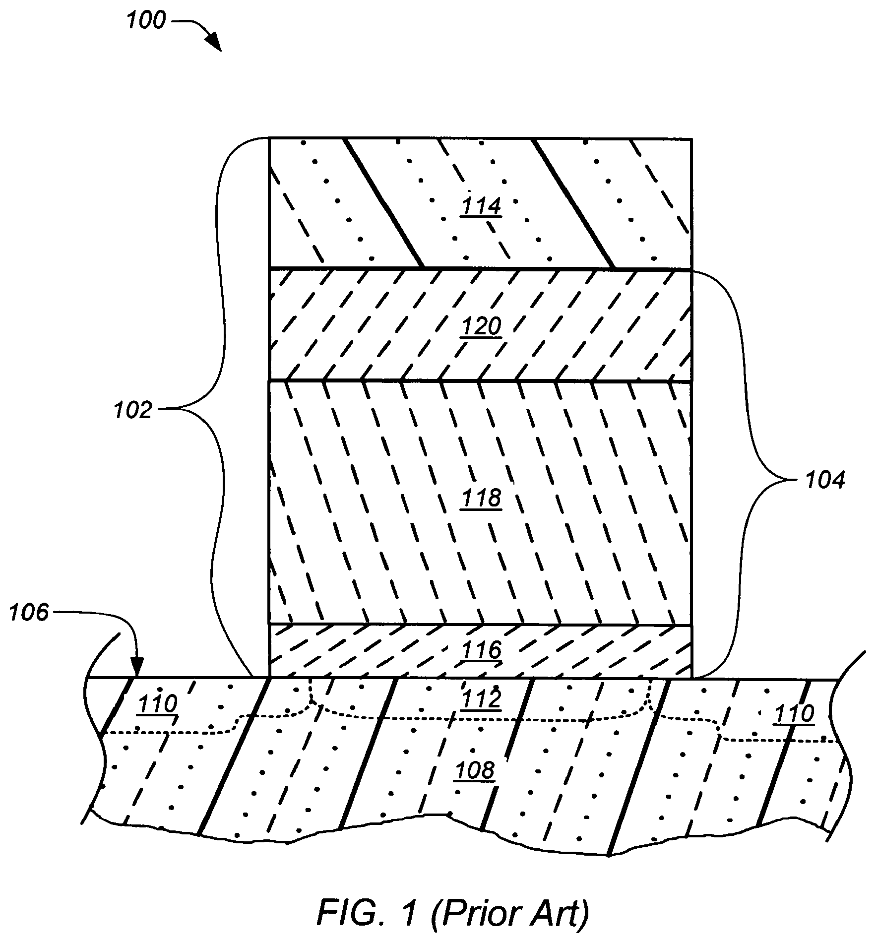
An oxide-nitride-oxide (ONO) stack is used as either a charge storing layer, as in silicon-oxide-nitride-oxide-silicon (SONOS) transistor, or as an isolation layer between the floating gate and control gate, as in a split gate flash memory.
FIG. 1 is a partial cross-sectional view of an intermediate structure for a semiconductor device 100 having a SONOS gate stack or structure 102 including a conventional ONO stack 104 formed over a surface 106 of a silicon substrate 108 according to a conventional method. In addition, the device 100 typically further includes one or more diffusion regions 110, such as source and drain regions, aligned to the gate stack and separated by a channel region 112. Briefly, the SONOS structure 102 includes a poly-silicon (poly) gate layer 114 formed upon and in contact with the ONO stack 104. The poly gate 114 is separated or electrically isolated from the substrate 108 by the ONO stack 104. The ONO stack 104 generally includes a lower oxide layer 116, a nitride or oxynitride layer 118 which serves as a charge storing or memory layer for the device 100, and a top, high-temperature oxide (HTO) layer 120 overlying the nitride or oxynitride layer.
One problem with conventional SONOS structures 102 and methods of forming the same is the poor data retention of the nitride or oxynitride layer 118 that limits the device 100 lifetime and/or its use in several applications due to leakage current through the layer.
Another problem with conventional SONOS structures 102 and methods of forming the same is the stochiometry of the oxynitride layer 118 is neither uniform nor optimized across the thickness of the layer. In particular, the oxynitride layer 118 is conventionally formed or deposited in a single step using a single process gas mixture and fixed or constant processing conditions in an attempt to provide a homogeneous layer having a high nitrogen and high oxygen concentration across the thickness of the relatively thick layer. However, due to top and bottom effects this results in nitrogen, oxygen and silicon concentrations, which can vary throughout the conventional oxynitride layer 118. The top effect is caused by the order in which process gases are shut off following deposition. In particular, the silicon containing process gas, such as silane, is typically shut off first resulting in a top portion of the oxynitride layer 118 that is high in oxygen and/or nitride and low in silicon. Similarly, the bottom effect is caused by the order in which process gases are introduced to initiate deposition. In particular, the deposition of the oxynitride layer 118 typically follows an annealing step, resulting in a peak or relatively high concentration (NH.sub.3) at the beginning of the deposition process and producing in a bottom portion of the oxynitride layer that is low in oxygen and silicon and high in nitrogen. The bottom effect is also due to surface nucleation phenomena in which that oxygen and silicon that is available in the initial process gas mixture preferentially reacts with silicon at the surface of the substrate and does not contribute to the formation of the oxynitride layer. Consequently, the charge storage characteristics, and in particular programming and erase speed and data retention of a memory device 100 made with the ONO stack 104, are adversely effected.
Accordingly, there is a need for a memory device having an ONO stack with an oxynitride layer as a memory layer that exhibits improved programming and erase speed and data retention. There is a further need for a method or process of forming an ONO stack having an oxynitride layer that exhibits improved oxynitride stochiometry.
The present invention provides a solution to these and other problems, and offers further advantages over conventional ONO stacks or memory layers and methods of forming the same.
BRIEF DESCRIPTION OF THE DRAWINGS
These and various other features and advantages of the present invention will be apparent upon reading of the following detailed description in conjunction with the accompanying drawings and the appended claims provided below, where:
FIG. 1 (prior art) is a block diagram illustrating a cross-sectional side view of an intermediate structure for a memory device for which a method having an oxide-nitride-oxide (ONO) stack formed according to conventional method;
FIG. 2 is a block diagram illustrating a cross-sectional side view of a portion of a semiconductor device having an ONO structure including a multi-layer charge storing layer according to an embodiment of the present invention;
FIG. 3 is flow chart of a method for forming an ONO structure including a multi-layer charge storing layer according to an embodiment of the present invention; and
FIG. 4 is a graph showing an improvement in data retention for a memory device using a memory layer formed according to the present invention as compared to a memory device using a conventional memory layer.
DETAILED DESCRIPTION
The present invention is directed generally to an oxide-nitride-oxide (ONO) structure including a multi-layer charge storing layer and methods for making the same. The ONO structure and method are particularly useful for forming a memory layer in a memory device, such as a silicon-oxide-nitride-oxide-silicon (SONOS) memory transistor.
In the following description, for purposes of explanation, numerous specific details are set forth in order to provide a thorough understanding of the present invention. It will be evident, however, to one skilled in the art that the present invention may be practiced without these specific details. In other instances, well-known structures, and techniques are not shown in detail or are shown in block diagram form in order to avoid unnecessarily obscuring an understanding of this description.
Reference in the description to "one embodiment" or "an embodiment" means that a particular feature, structure, or characteristic described in connection with the embodiment is included in at least one embodiment of the invention. The appearances of the phrase "in one embodiment" in various places in the specification do not necessarily all refer to the same embodiment. The term "to couple" as used herein may include both to directly connect and to indirectly connect through one or more intervening components.
Briefly, the method involves forming a multi-layer charge storing layer including multiple oxynitride layers, such as silicon oxynitride (Si.sub.2N.sub.2O) layers, having differing concentrations of Oxygen, Nitrogen and/or Silicon. Generally, the oxynitride layers are formed at higher temperatures than nitride or oxynitride layers in conventional ONO structures, and each of the layers are formed using differing process gases mixtures and/or at differing flow rates. Preferably, the oxynitride layers include at least a top oxynitride layer and a bottom oxynitride layer. More preferably, the stochiometric compositions of the layers is tailored or selected such that the lower or bottom oxynitride has a high oxygen and silicon content, and the top oxynitride layer has high silicon and a high nitrogen concentration with a low oxygen concentration to produce a silicon-rich nitride or oxynitride. The silicon-rich and oxygen-rich bottom oxynitride layer reduces stored charge loss without compromising device speed or an initial (beginning of life) difference between program and erase voltages. The silicon-rich, oxygen-lean top oxynitride layer increases a difference between programming and erase voltages of memory devices, thereby improving device speed, increasing data retention, and extending the operating life of the device.
Optionally, the ratio of thicknesses between the top oxynitride layer and the bottom oxynitride layer can be selected to facilitate forming of the oxynitride layers over a first oxide layer of an ONO structure following the step of forming the first oxide layer using a steam anneal.
An ONO structure and methods for fabricating the same according to various embodiments of the present invention will now be described in greater detail with reference to FIGS. 2 through 4.
FIG. 2 is a block diagram illustrating across-sectional side view of a portion of a semiconductor memory device 200 having an ONO structure including a multi-layer charge storing layer according to one embodiment of the present invention. Referring to FIG. 2, the memory device 200 includes a SONOS gate stack 202 including an ONO structure 204 formed over a surface 206 of silicon layer on a substrate or a silicon substrate 208. In addition, the device 200 further includes one or more diffusion regions 210, such as source and drain regions, aligned to the gate stack 202 and separated by a channel region 212. Generally, the SON structure 202 includes a poly-silicon or poly gate layer 214 formed upon and in contact with the ONO structure 204 and a portion of the silicon layer or substrate 208. The poly gate 214 is separated or electrically isolated from the substrate 208 by the ONO structure 204. The ONO structure 204 includes a thin, lower oxide layer or tunneling oxide layer 216 that separates or electrically isolates the gate stack 202 from the channel region 212, a top or blocking oxide layer 218, and a multi-layer charge storing layer including multiple nitride containing layers. Preferably, as noted above and as shown in FIG. 2, the multi-layer charge storing layer includes at least two oxynitride layers, including a top oxynitride layer 220A and a bottom oxynitride layer 220B.
Generally, the substrate 208 may include any known silicon-based semiconductor material including silicon, silicon-germanium, silicon-on-insulator, or silicon-on-sapphire substrate. Alternatively, the substrate 208 may include a silicon layer formed on a non-silicon-based semiconductor material, such as gallium-arsenide, germanium, gallium-nitride, or aluminum-phosphide. Preferably, the substrate 208 is a doped or undoped silicon substrate.
The lower oxide layer or tunneling oxide layer 216 of the ONO structure 204 generally includes a relatively thin layer of silicon dioxide (SiO.sub.2) of from about 15 angstrom (.ANG.) to about 22 .ANG., and more preferably about 18 .ANG.. The tunneling oxide layer 216 can be formed or deposited by any suitable means including, for example, being thermally grown or deposited using chemical vapor deposition (CVD). In a preferred embodiment, the tunnel oxide layer is formed or grown using a steam anneal. Generally, the process involves a wet-oxidizing method in which the substrate 208 is placed in a in a deposition or processing chamber, heated to a temperature from about 700.degree. C. to about 850.degree. C., and exposed to a wet vapor for a predetermined period of time selected based on a desired thickness of the finished tunneling oxide layer 216. Exemplary process times are from about 5 to about 20 minutes. The oxidation can be performed at atmospheric or at low pressure.
As noted above, the multi-layer charge storing layer generally includes at least two oxynitride layers having differing compositions of silicon, oxygen and nitrogen, and can have an overall thickness of from about 70 .ANG. to about 150 .ANG., and more preferably about 100 .ANG.. In a preferred embodiment the oxynitride layers are formed or deposited in a low pressure CVD process using a silicon source, such as slime (SiH.sub.4), chlorosilane (SiH.sub.3Cl), dichlorosilane (SiH.sub.2Cl.sub.2), tetrachlorosilane (SiCl.sub.4) or BisTertiaryButylAmino Silane (BTBAS), a nitrogen source, such as nitrogen ammonia (NH.sub.3), nitrogen trioxide (NO.sub.3) or nitrous oxide (N.sub.2O), and an oxygen-containing gas, such as oxygen (O.sub.2) or N.sub.2O. Alternatively, gases in which hydrogen has been replaced by deuterium can be used, including, for example, the substitution of deuterated-ammonia (ND.sub.3) for NH.sub.3. The substitution of deuterium for hydrogen advantageously passivates Si dangling bonds at the silicon-oxide interface, thereby increasing an NBTI (Negative Bias Temperature Instability) lifetime of the devices.
For example, the lower or bottom oxynitride layer 220B can be deposited over the tunneling oxide layer 216 by placing the substrate 208 in a deposition chamber and introducing a process gas including N.sub.2O, NH.sub.3 and DCS, while maintaining the chamber at a pressure of from about 5 millitorr (mT) to about 500 mT, and maintaining the substrate at a temperature of from about 700.degree. C. to about 850.degree. C. and more preferably at least about 780.degree. C., for a period of from about 2.5 minutes to about 20 minutes. In particular, the process gas can include a first gas mixture of N.sub.2O and NH.sub.3 mixed in a ratio of from about 8:1 to about 1:8 and a second gas mixture of DCS and NH.sub.3 mixed in a ratio of from about 1:7 to about 7:1, and can be introduced at a flow rate of from about 5 to about 200 standard cubic centimeters per minute (sccm). It has been found that an oxynitride layer produced or deposited under these condition yields a silicon-rich, oxygen-rich, bottom oxynitride layer 220B, that decrease the charge loss rate after programming and after erase, which is manifested in a small voltage shift in the retention mode.
The top oxynitride layer 220A can be deposited over the bottom oxynitride layer 220B in a CVD process using a process gas including N.sub.2O, NH.sub.3 and DCS, at a chamber pressure of from about 5 mT to about 500 mT, and at a substrate temperature of from about 700.degree. C. to about 850.degree. C. and more preferably at least about 780.degree. C., for a period of from about 2.5 minutes to about 20 minutes. In particular, the process gas can include a first gas mixture of N.sub.2O and NH.sub.3 mixed in a ratio of from about 8:1 to about 1:8 and a second gas mixture of DCS and NH.sub.3 mixed in a ratio of from about 1:7 to about 7:1, and can be introduced at a flow rate of from about 5 to about 20 sccm. It has been found that an oxynitride layer produced or deposited under these condition yields a silicon-rich, nitrogen-rich, and oxygen-lean top oxynitride layer 220A, which it proves the speed and increases of the initial difference between program and erase voltage without compromising a charge loss rate of memory devices made using an embodiment of the inventive ONO structure 204, thereby extending the operating life of the device.
Preferably, the top oxynitride layer 220A is deposited sequentially in the same tool used to form the bottom oxynitride layer 220B, substantially without breaking vacuum on the deposition chamber. More preferably, the top oxynitride layer 220A is deposited substantially without altering the temperature to which the substrate 208 was heated during deposition of the bottom oxynitride layer 220B. In one embodiment, the top oxynitride layer 220A is deposited sequentially and immediately following the deposition of the bottom oxynitride layer 220B by decreasing the flow rate of the N.sub.2O/NH.sub.3 gas mixture relative to the DCS/NH.sub.3 gas mixture to provide the desired ratio of the gas mixtures to yield the silicon-rich, nitrogen-rich, and oxygen-lean top oxynitride layer 220A.
In certain embodiments, another oxide or oxide layer (not shown in these figures) is formed after the formation of the ONO structure 204 in a different area on the substrate or in the device using a steam oxidation. In this embodiment, the top oxynitride layer 220A and top oxide layer 218 of the ONO structure 204 are beneficially steam annealed during the steam oxidation process. In particular, steam annealing improves the quality of the top oxide layer 218 reducing the number of traps formed near a top surface of the top oxide layer and near a top surface of the underlying top oxynitride layer 220A, thereby reducing or substantially eliminating an electric field that could otherwise form across the top oxide layer, which could result in back streaming of charge carriers therethrough and adversely affecting data or charge retention in the charge storing layer.
A suitable thickness for the bottom oxynitride layer 220B has been found to be from about 10 .ANG. to about 80 .ANG., and a ratio of thicknesses between the bottom layer and the top oxynitride layer has been found to be from about 1:6 to about 6:1, and more preferably at least about 1:4.
The top oxide layer 218 of the ONO structure 204 includes a relatively thick layer of SiO.sub.2 of from about 30 .ANG. to about 70 .ANG., and more preferably about 45 .ANG.. The top oxide layer 218 can be formed or deposited by any suitable means including, for example, being thermally grown or deposited using CVD. In a preferred embodiment, the top oxide layer 218 is a high-temperature-oxide (HTO) deposited using CVD process. Generally, the deposition process involves exposing the substrate 208 to a silicon source, such as silane, chlorosilane, or dichlorosilane, and an oxygen-containing gas, such as O.sub.2 or N.sub.2O in a deposition chamber at a pressure of from about 50 mT to about 1000 mT, for a period of from about 10 minutes to about 120 minutes while maintaining the substrate at a temperature of from about 650.degree. C. to about 850.degree. C.
Preferably, the top oxide layer 218 is deposited sequentially in the same tool used to form the oxynitride layers 220A, 220B. More preferably, the oxynitride layers 220A, 220B, and the top oxide layer 218 are formed or deposited in the same tool used to grow the tunneling oxide layer 216. Suitable tools include, for example, an ONO AVP, commercially available from AVIZA technology of Scotts Valley, Calif.
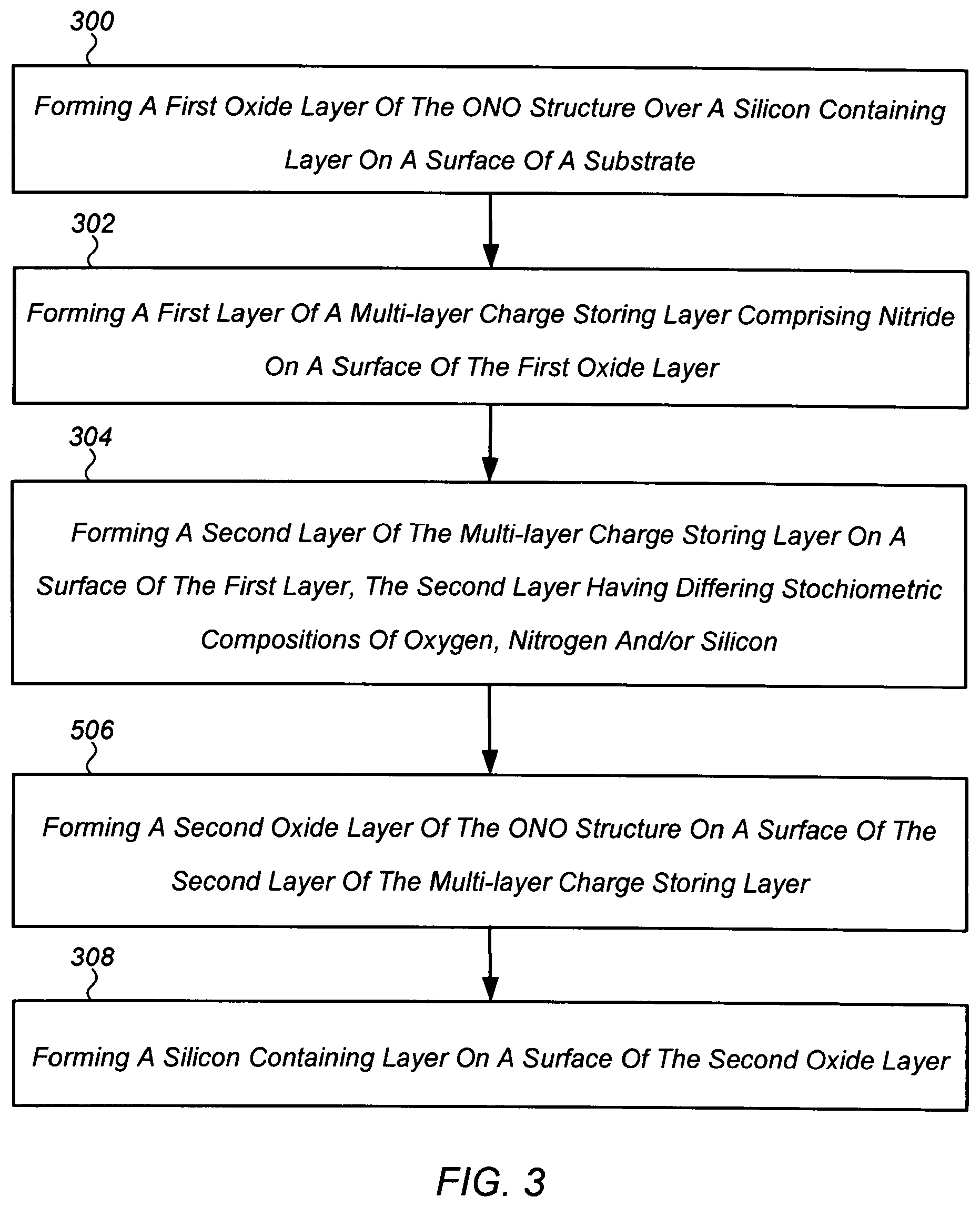
A method or forming or fabricating an ONO stack according to one embodiment of the present invention will now be described with reference to the flowchart of FIG. 3.
Referring to FIG. 3, the method begins with forming a first oxide layer, such as a tunneling oxide layer, of the ONO structure over a silicon containing layer on a surface of a substrate (step 300). Next, the first layer of a multi-layer charge storing layer including nitride is formed on a surface of the first oxide layer (step 302). As noted above, this first layer or bottom oxynitride layer can be formed or deposited by a CVD process using a process gas including N.sub.2O/NH.sub.3 and DCS/NH.sub.3 gas mixtures in ratios and at flow rates tailored to provide a silicon-rich and oxygen-rich oxynitride layer. The second layer of the multi-layer charge storing layer is then formed on a surface of the first layer (step 304). The second layer has a stochiometric composition of oxygen, nitrogen and/or silicon different from that of the first layer. In particular, and as noted above, the second or top oxynitride layer can be formed or deposited by a CVD process using a process gas including DCS/NH.sub.3 and N.sub.2O/NH.sub.3 gas mixtures in ratios and at flow rates tailored to provide a silicon-rich, oxygen-lean top oxynitride layer. Finally, a second oxide layer of the ONO structure is formed on a surface of the second layer of the multi-layer charge storing layer (step 306). As noted above, this top or blocking oxide layer can be formed or deposited by any suitable means, but is preferably deposited in a CVD process. In one embodiment the top or second oxide layer is a high temperature oxide deposited in a HTO CVD process. Alternatively, the top or blocking oxide layer can be thermally grown, however it will be appreciated that in this embodiment the oxynitride thickness must be adjusted or increased as some of the top oxynitride will be effectively consumed or oxidized during the process of thermally growing the blocking oxide layer.
Optionally, the method may further include the step of forming or depositing a silicon containing layer on a surface of the second oxide layer to form a SONOS stack or structure (step 308). The silicon containing layer can be, for example, a polysilicon layer deposited by a CVD process to form a control gate of a SONOS transistor or device.
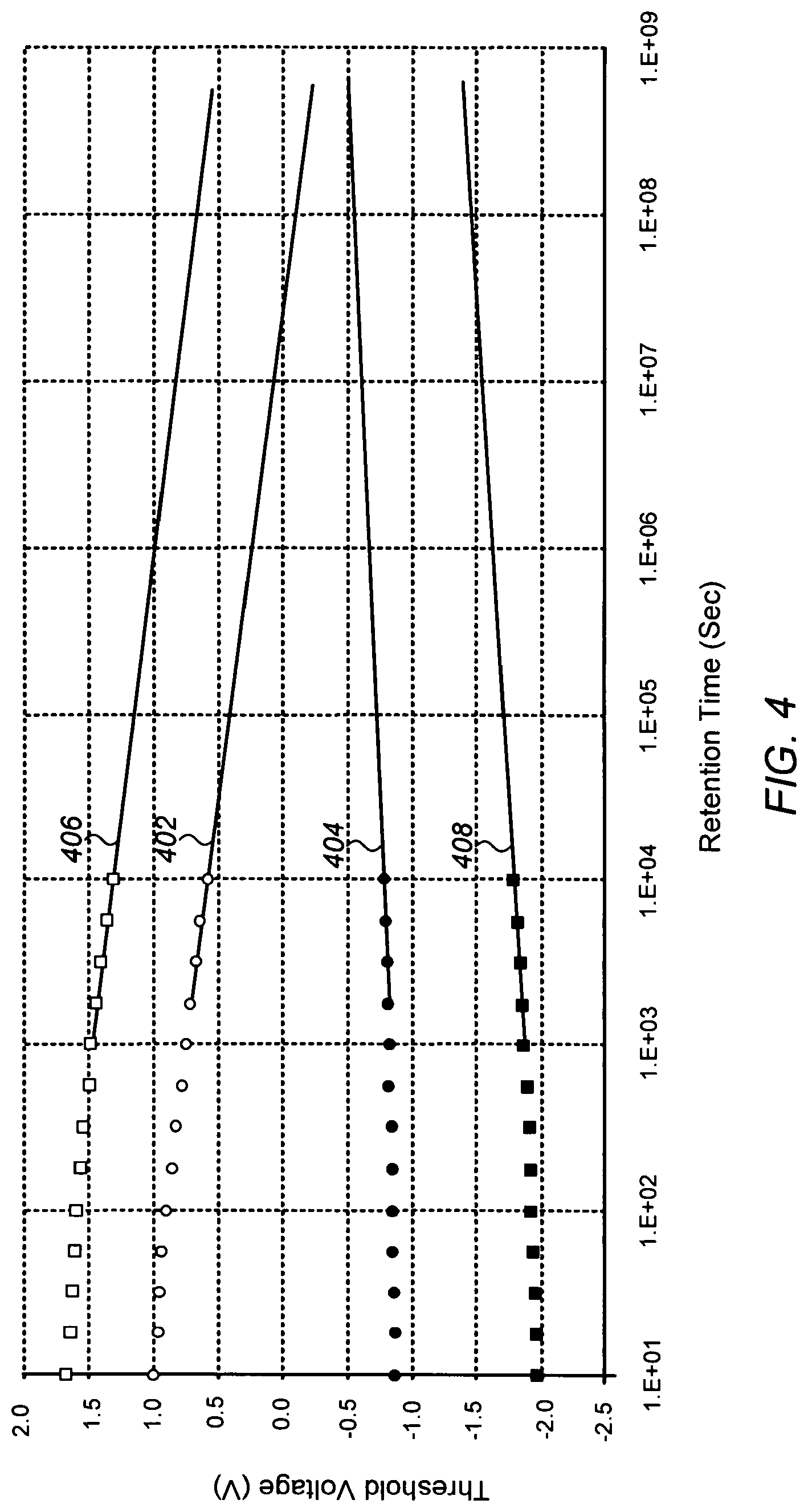
A comparison of data retention for a memory device using a memory layer formed according to an embodiment of the present invention as compared to a memory device using a conventional memory layer will now be made with reference to FIG. 4. In particular, FIG. 4 illustrates the change in threshold voltage of devices in an electronically erasable programmable read-only memory (EEPROM) during programming (VTP) during erase (VTE) over device life for an EEPROM made using a conventional ONO structure and an ONO structure having a multi-layer oxynitride layer. In gathering data for this figure both devices were pre-cycled for 100K cycles at an ambient temperature of 85.degree. C.
Referring to FIG. 4, the graph or line 402 illustrates the change over time of a VIP for an EEPROM made using a conventional ONO structure having a single oxynitride layer without refreshing the memory after the initial writing--program or erase. Actual data points on line 402 are shown by unfilled circles, the remainder of the line showing an extrapolation of VTP to a specified end-of-life (EOL) for the EEPROM. Graph or line 404 illustrates the change over time of a VTE for the EEPROM made using a conventional ONO structure. Actual data points on line 404 are shown by filled circles, and the remainder of the line shows an extrapolation of VTE to EOL for the EEPROM. Generally, the specified difference between the VTE and VTP for an EEPROM at EOL is at least 0.5 V to be able to identify or sense the difference between the program and erase state. As seen from this figure an EEPROM made using a conventional ONO structure has a difference between VTE and VTP of about 0.35V at a specified EOL of 20 years. Thus, an EEPROM made using a conventional ONO structure and operated under the conditions described above will fail to meet the specified operating life by at least about 17 years.
In contrast, the change in VTP and VTE over time for an EEPROM made using an ONO structure having a multi-layer oxynitride layer, illustrated by lines 406 and 408 respectively, shows a difference between VTE and VTP of at least about 1.96V at the specified EOL. Thus, an EEPROM made using an ONO structure according to an embodiment of the present invention will meet and exceed the specified operating life of 20 years. In particular, graph or line 406 illustrates the change over time VTP for an EEPROM using an ONO structure according to an embodiment of the present invention. Actual data points on line 406 are shown by unfilled squares, the remainder of the line showing an extrapolation of VTP to the specified EOL. Graph or line 408 illustrates the change over time of VTE for the EEPROM, and actual data points on line 408 are shown by filled squares, the remainder of the line showing an extrapolation of VTE to EOL.
Although shown and described above as having only two oxynitride layer, i.e., a top and a bottom layer, the present invention is not so limited, and the multi-layer charge storing layer can include any number, n, of oxynitride layers, any or all of which may have differing stochiometric compositions of oxygen, nitrogen and/or silicon. In particular, multi-layer charge storing layers having up to five oxynitride layers each with differing stochiometric compositions have been produced and tested. However, as will be appreciated by those skilled in the art it is generally desirable to utilize as few layers as possible to accomplish a desired result, reducing the process steps necessary to produce the device, and thereby providing a much simpler and more robust manufacturing process. Moreover, utilizing as few layers as possible also results in higher yields as it is simpler to control the stoichiometric composition and dimensions of the fewer layers.
It will further be appreciated that although shown and described as part of a SONOS stack in a SONOS memory device, the ONO structure and method of the present invention is not so limited, and the ONO structure can be used in or with any semiconductor technology or in any device requiring a charge storing or dielectric layer or stack including, for example, in a split gate flash memory, a TaNOS stack, in a 1T (transistor) SONOS cell, a 2T SONOS cell, a 3T SONOS cell, a localized 2-bit cell, and in a multilevel programming or cell, without departing from the scope of the invention.
The advantages of ONO structures and methods of forming the same according to an embodiment of the present invention over previous or conventional approaches include:(i) the ability to enhance data retention in memory devices using the structure by dividing the oxynitride layer into a plurality of films or layers and tailoring the oxygen, nitrogen and silicon profile across each layer; (ii) the ability to enhance speed of a memory device without compromising data retention; (iii) the ability to meet or exceed data retention and speed specifications for memory devices using an ONO structure of an embodiment of the present invention at a temperature of at least about 125.degree. C.; and (iv) provide heavy duty program erase cycles of 100,000 cycles or more.
The foregoing description of specific embodiments and examples of the invention have been presented for the purpose of illustration and description, and although the invention has been described and illustrated by certain of the preceding examples, it is not to be construed as being limited thereby. They are not intended to be exhaustive or to limit the invention to the precise forms disclosed, and many modifications, improvements and variations within the scope of the invention are possible in light of the above teaching. It is intended that the scope of the invention encompass the generic area as herein disclosed, and by the claims appended hereto and their equivalents. The scope of the present invention is defined by the claims, which includes known equivalents and unforeseeable equivalents at the time of filing of this application.
* * * * *
References
D00000
D00001
D00002
D00003
D00004
XML
uspto.report is an independent third-party trademark research tool that is not affiliated, endorsed, or sponsored by the United States Patent and Trademark Office (USPTO) or any other governmental organization. The information provided by uspto.report is based on publicly available data at the time of writing and is intended for informational purposes only.
While we strive to provide accurate and up-to-date information, we do not guarantee the accuracy, completeness, reliability, or suitability of the information displayed on this site. The use of this site is at your own risk. Any reliance you place on such information is therefore strictly at your own risk.
All official trademark data, including owner information, should be verified by visiting the official USPTO website at www.uspto.gov. This site is not intended to replace professional legal advice and should not be used as a substitute for consulting with a legal professional who is knowledgeable about trademark law.