Package structure
Lin , et al.
U.S. patent number 10,727,202 [Application Number 15/347,803] was granted by the patent office on 2020-07-28 for package structure. This patent grant is currently assigned to MediaTek Inc.. The grantee listed for this patent is MEDIATEK INC.. Invention is credited to Wei-Che Huang, Yu-Hua Huang, Tzu-Hung Lin, Ming-Tzong Yang.


| United States Patent | 10,727,202 |
| Lin , et al. | July 28, 2020 |
Package structure
Abstract
A package structure comprising: a substrate, having at least one conductive units provided at a first surface of the substrate; at least one first die, provided on a second surface of the substrate; a connecting layer, provided on the first die; a second die, provided on the connecting layer, wherein the connecting layer comprises at least one bump for connecting the first die; and at least one bonding wire. The connecting layer has a first touch side and a second touch side, the first touch side contacts a first surface of the first die and the second touch side contacts a second surface of the second die, an area of the first touch side is smaller than which for the first surface of the first die, and a size of the first die equals to which of the second die.
| Inventors: | Lin; Tzu-Hung (Hsinchu County, TW), Huang; Yu-Hua (Hsinchu, TW), Huang; Wei-Che (Hsinchu County, TW), Yang; Ming-Tzong (Hsinchu County, TW) | ||||||||||
|---|---|---|---|---|---|---|---|---|---|---|---|
| Applicant: |
|
||||||||||
| Assignee: | MediaTek Inc. (Hsin-Chu,
TW) |
||||||||||
| Family ID: | 52739302 | ||||||||||
| Appl. No.: | 15/347,803 | ||||||||||
| Filed: | November 10, 2016 |
Prior Publication Data
| Document Identifier | Publication Date | |
|---|---|---|
| US 20170062388 A1 | Mar 2, 2017 | |
Related U.S. Patent Documents
| Application Number | Filing Date | Patent Number | Issue Date | ||
|---|---|---|---|---|---|
| 14040732 | Sep 30, 2013 | 9524948 | |||
| Current U.S. Class: | 1/1 |
| Current CPC Class: | H01L 25/0657 (20130101); H01L 24/73 (20130101); H01L 24/16 (20130101); H01L 24/48 (20130101); H01L 24/32 (20130101); H01L 2225/06562 (20130101); H01L 2225/0651 (20130101); H01L 2224/32105 (20130101); H01L 2224/73215 (20130101); H01L 2924/00014 (20130101); H01L 2924/1431 (20130101); H01L 2224/32058 (20130101); H01L 2224/48227 (20130101); H01L 2924/15311 (20130101); H01L 2225/06568 (20130101); H01L 2224/32014 (20130101); H01L 2224/73207 (20130101); H01L 2225/06565 (20130101); H01L 2924/1434 (20130101); H01L 2224/16145 (20130101); H01L 2224/73204 (20130101); H01L 2224/32145 (20130101); H01L 2225/06513 (20130101); H01L 25/18 (20130101); H01L 2924/00014 (20130101); H01L 2224/45099 (20130101); H01L 2924/00014 (20130101); H01L 2224/45015 (20130101); H01L 2924/207 (20130101); H01L 2224/73204 (20130101); H01L 2224/16145 (20130101); H01L 2224/32145 (20130101); H01L 2924/00 (20130101); H01L 2924/00014 (20130101); H01L 2224/05599 (20130101); H01L 2924/00014 (20130101); H01L 2224/85399 (20130101) |
| Current International Class: | H01L 23/48 (20060101); H01L 25/065 (20060101); H01L 23/00 (20060101); H01L 25/18 (20060101) |
| Field of Search: | ;257/737,673,678,E23.021,E23.033,E23.068,E23.069,E21.508 |
References Cited [Referenced By]
U.S. Patent Documents
| 2003/0110625 | June 2003 | Fang |
| 2004/0251531 | December 2004 | Yang |
| 2005/0170600 | August 2005 | Fukuzo |
| 2007/0057357 | March 2007 | Chen |
| 2007/0228543 | October 2007 | Walter |
| 2011/0180913 | July 2011 | Liou |
| 2012/0187560 | July 2012 | Choi et al. |
| 2012/0276691 | November 2012 | Camacho |
| 2013/0147025 | June 2013 | Liou |
| 2013/0161788 | June 2013 | Chun |
| 2014/0042600 | February 2014 | Kim |
| 1391278 | Jan 2003 | CN | |||
| 1649149 | Aug 2005 | CN | |||
| 102136434 | Jul 2011 | CN | |||
| 103178054 | Jun 2013 | CN | |||
| 2007-207805 | Aug 2007 | JP | |||
| 2013105153 | Jul 2013 | WO | |||
| WO 2013/105153 | Jul 2013 | WO | |||
Attorney, Agent or Firm: Wolf, Greenfield & Sacks, P.C.
Parent Case Text
CROSS REFERENCE TO RELATED APPLICATION
This application is a continuation application of applicant's earlier application, Ser. No. 14/040,732, filed 2013 Sep. 30, and is included herein by reference.
Claims
What is claimed is:
1. A package structure, comprising: a substrate, having a plurality of conductive units provided at a first surface of the substrate; a first die, provided on a second surface of the substrate; a connecting layer, provided on the first die; a second die, provided on the connecting layer, wherein the connecting layer comprises a bump for connecting the first die to the second die such that the first die and the second die are electrically connected; and a bonding wire, for electrically connecting the first die to the plurality of conductive units or the substrate; wherein the connecting layer has a first touch side and a second touch side, wherein the first touch side contacts a first surface of the first die and the second touch side contacts a second surface of the second die, wherein an edge of the second touch side of the connecting layer is aligned with an edge of the second surface of the second die, and wherein an area of the first touch side is smaller than an area of the first surface of the first die, wherein a size of the first die equals to a size of the second die.
2. The package structure of claim 1, wherein the first die is a memory die and the second die is a logic die.
3. The package structure of claim 1, wherein the first die is a logic die and the second die is a memory die.
4. The package structure of claim 1, wherein an area of the second touch side equals to an area for the second surface of the second die.
5. The package structure of claim 1, wherein a projected image of the second die does not totally contain the first die.
6. The package structure of claim 5, wherein a location for the first die or the second die is shifted.
7. The package structure of claim 6, wherein the bonding wire is only provided at one side of the first die.
8. The package structure of claim 6, wherein the bonding wire is provided at two sides of the first die.
9. The package structure of claim 1, wherein the connecting layer is generated via a flip chip process.
10. A package structure, comprising: a substrate, having a plurality of conductive units provided at a first surface of the substrate; a first die, provided on a second surface of the substrate; a connecting layer, provided on the first die; a second die, provided on the connecting layer, wherein the connecting layer comprises a bump for connecting the first die to the second die such that the first die and the second die are electrically connected; and a bonding wire, for electrically connecting the first die to the plurality of conductive units or the substrate; wherein the connecting layer has a first touch side and a second touch side, wherein the first touch side contacts a first surface of the first die and the second touch side contacts a second surface of the second die, wherein an edge of the second touch side of the connecting layer is aligned with an edge of the second surface of the second die, and wherein a location for the first die or the second die is shifted.
11. The package structure of claim 10, wherein the first die is a memory die and the second die is a logic die.
12. The package structure of claim 10, wherein the first die is a logic die and the second die is a memory die.
13. The package structure of claim 10, wherein a size of the first die is larger than which of the second die.
14. The package structure of claim 10, wherein a size of the first die equals to a size of the second die.
15. The package structure of claim 10, wherein the connecting layer has a first touch side and a second touch side, wherein the first touch side contacts a first surface of the first die and the second touch side contacts a second surface of the second die, where an area of the first touch side is smaller than the first surface of the first die.
16. The package structure of claim 10, where an area of the second touch side equals to an area of the second surface of the second die.
17. The package structure of claim 10, where an area of the second touch side is smaller than an area of the second surface of the second die.
18. The package structure of claim 10, wherein a projected image of the second die does not totally contain the first die.
19. The package structure of claim 10, wherein the bonding wire is only provided at one side of the first die.
20. The package structure of claim 10, wherein the connecting layer comprises: a metal layer located between the first die and the second die, wherein part of the metal layer comprises metal: and at least one micro bump, for connecting the first die and the second die.
Description
BACKGROUND
A wide I/O memory device is a memory device having pins more than other kinds of memory devices. The wide I/O memory device can have a rapid data accessing speed, since it has large number of pins to access data.
FIG. 1 is a cross sectional diagram illustrating a semiconductor structure for a related art wide I/O memory device. As shown in FIG. 1, the wide I/O memory device 100 has a memory cube MC and a logic die LI provided on a substrate Su. The memory cube MC comprises a plurality of memory dies MI. Vias VA (only one is marked by the symbol) are generated via a TSV (Through-Silicon Via) process, such that the memory cube MC and a logic die LI can be electrically connected to the conductive units Cu (ex. solder ball) or the substrate Su. However, the I/O memory device needs plenty of vias since it has many pins, but the TSV process causes high cost. Therefore, the cost for the I/O memory device is extremely high.
SUMMARY
Therefore, one objective of the present application is to provide a package structure that can be generated without the TSV process.
One embodiment of the present application provides a package structure, which comprises: a substrate, having at least one conductive units provided at a first surface of the substrate; at least one first die, provided on a second surface of the substrate; a connecting layer, provided on the first die; a second die, provided on the connecting layer, wherein the connecting layer comprises at least one bump for connecting the first die to the second die such that the first die and the second die are electrically connected; and at least one bonding wire, for electrically connecting the first die to the conductive units or the substrate. The connecting layer has a first touch side and a second touch side, the first touch side contacts a first surface of the first die and the second touch side contacts a second surface of the second die, an area of the first touch side is smaller than which for the first surface of the first die, and a size of the first die equals to which of the second die.
Another embodiment of the present application provides a package structure, which comprises: a substrate, having at least one conductive units provided at a first surface of the substrate; at least one first die, provided on a second surface of the substrate; a connecting layer, provided on the first die; a second die, provided on the connecting layer, wherein the connecting layer comprises at least one bump for connecting the first die to the second die such that the first die and the second die are electrically connected; and at least one bonding wire, for electrically connecting the first die to the conductive units or the substrate. A location for the first die or the second die is shifted.
In view of above-mentioned embodiments, a package structure can be produced without performing TSV processes. Therefore, the cost can be largely reduced.
These and other objectives of the present invention will no doubt become obvious to those of ordinary skill in the art after reading the following detailed description of the preferred embodiment that is illustrated in the various figures and drawings.
BRIEF DESCRIPTION OF THE DRAWINGS
FIG. 1 is a cross sectional diagram illustrating a semiconductor structure for a related art wide I/O memory device.
FIG. 2 is a cross sectional diagram illustrating a package structure according to one embodiment of the present application.
FIG. 3 is a cross sectional diagram illustrating detail structures for the embodiment shown in FIG. 2 of the present application.
FIG. 4-FIG. 8 are cross sectional diagrams illustrating a package structure according to different embodiments of the present application.
DETAILED DESCRIPTION
The package structure according to the present application will be explained for detail below. Please note the package structure according to the present application is not only can be applied to the above-mentioned wide I/O memory device, but also can be applied to other electronic devices.
FIG. 2 is a cross sectional diagram illustrating a package structure 200 according to one embodiment of the present application.
As shown in FIG. 2, the package structure 200 comprises a substrate Su, a first die DI.sub.1, a connecting layer BL, a second die DI.sub.2 and at least one bonding wire WB. The substrate Su having at least one conductive unit Cu (only one of them is marked by a symbol) provided on a first surface S.sub.1 thereof. The first die DI.sub.1 is provided on a second surface S.sub.2 of the substrate Su. The connecting layer BL is provided on the first die DI.sub.1, and is for electrically bumping the first die DI.sub.1 to the second die DI.sub.2. In one embodiment, the connecting layer BL comprises at least one bump for electrically connecting the first die DI.sub.1 to the second die DI.sub.2. The at least one bonding wire WB is for connecting the first die DI.sub.1 and the conductive units Cu, or connecting the first die DI.sub.1 and the substrate Su. In one embodiment, the bonding wire WB is connected to via V formed in the substrate Su, which is electrically connected to the conductive unit Cu, but is not limited. Also, in the embodiment illustrated in FIG. 2, the size of the first die DI.sub.1 is larger than which of the second die DI.sub.2.
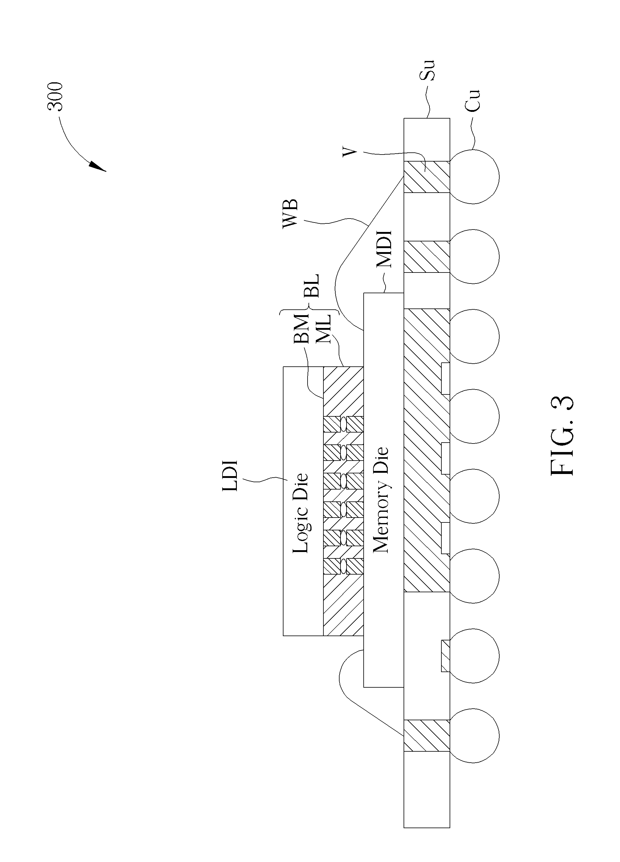
FIG. 3 is a cross sectional diagram illustrating detail structures for the embodiment shown in FIG. 2 of the present application. As shown in FIG. 3, the first die of the package structure 300 is a memory die MDI and the second die is a logic die LDI. Please note the kinds of dies can be swapped. That is, the first die can be a logic die LDI and the second die can be a memory die MDI. Additionally, in one embodiment the connecting layer BL is generated via a flip chip process. In another embodiment, the connecting layer BL comprises a metal layer ML located between the memory die MDI and the logic die LDI, and at least one micro bump BM for connecting the memory die MDI and the logic die LDI. Also, in such embodiment, the metal layer ML is a redistribution layer (RDL). Please note the package structure according to the present application can include only part of the structures described in FIG. 3. For example, the first die and the second die can be other kinds of dies besides the memory die and the logic die, but the connecting layer BL can still comprise a metal layer ML, and the micro bump BM.
FIG. 4-FIG. 8 are cross sectional diagrams illustrating a package structure according to different embodiments of the present application.
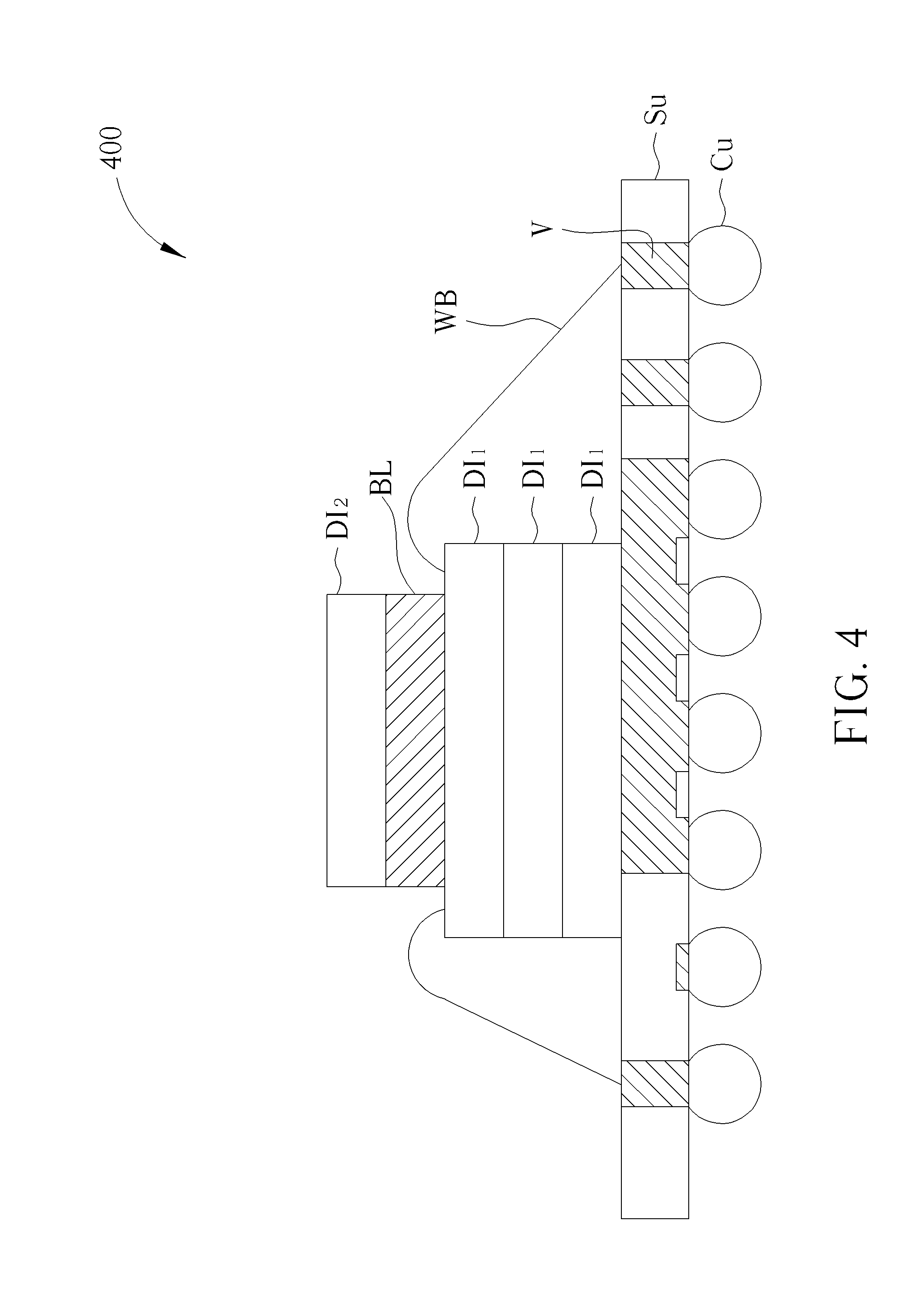
In FIG. 4, the package structure 400 comprises more than one first die DI.sub.1 located between the connecting layer BL and the substrate Su. If the package structure 400 is a wide I/O memory device, the first dies can be memory dies to form a memory cube.
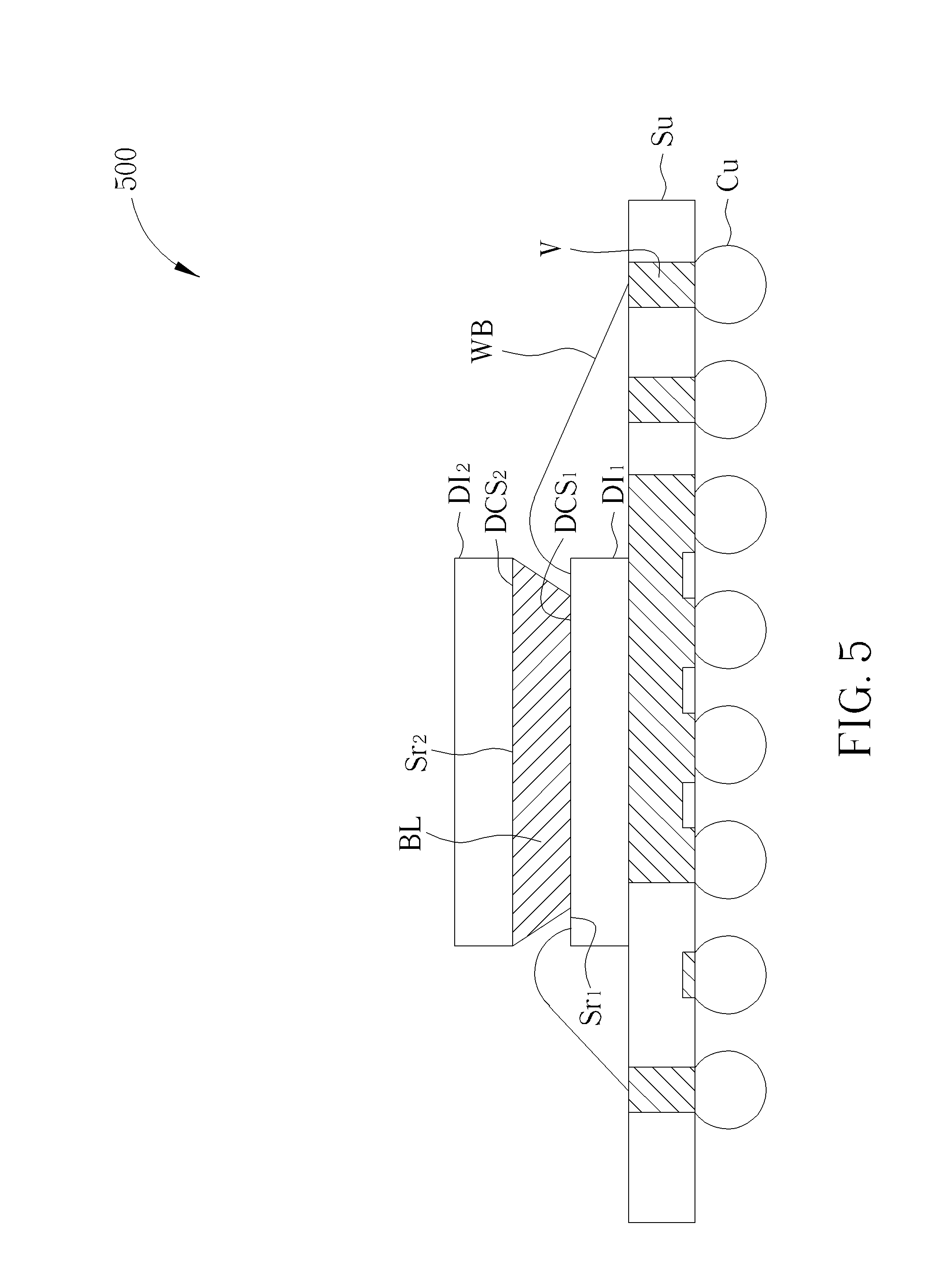
In the package structure 500 of FIG. 5, the sizes of the first die DI.sub.1 and the second die DI.sub.2 are the same, and the connecting layer BL has a first touch side DCS.sub.1 and a second touch side DCS.sub.2. The first touch side DCS.sub.1 contacts a first surface Sr.sub.1 of the first die DI.sub.1 and the second touch side DCS.sub.2 contacts a second surface Sr.sub.2 of the second die DI.sub.2. Also, in FIG. 5 an area of the first touch side DCS.sub.1 is smaller than which for the first surface Sr.sub.1 of the first die DI.sub.1, and an area of the second touch side DCS.sub.2 equals to which for the second surface Sr.sub.2 of the second die DI.sub.2.
The structure shown in FIG. 6 is almost the same as which of FIG. 5, one difference is that the area of the second touch side DCS.sub.2 equals to which for the second surface Sr.sub.2 of the second die DI.sub.2 for the package structure 500 in FIG. 5, but the area for the second touch side DCS.sub.2 is smaller than which for the second surface Sr.sub.2 of the second die DI.sub.2 for the package structure 600 in FIG. 6.
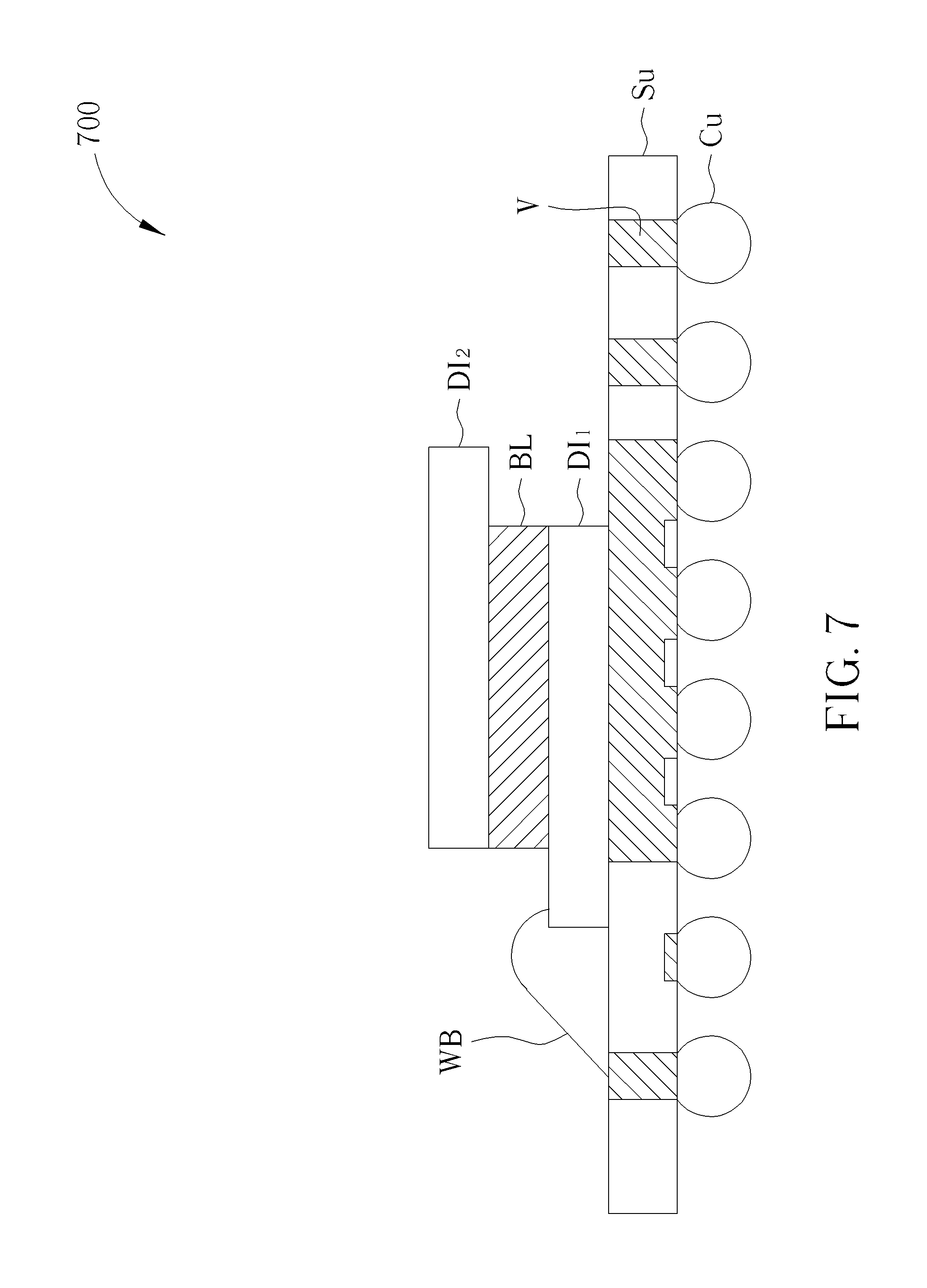
In the embodiments described in FIG. 7 and FIG. 8, the sizes of the first die DI.sub.1 and the second die DI.sub.2 are the same as well, but the location for the first die DI.sub.1 or the second die DI.sub.2 is shifted such that a projected image of the second die DI.sub.2 does not totally contain the first die DI.sub.1. In the embodiment described in FIG. 7, bonding wire WB is only provided to one side of the first die DI.sub.1. In the embodiment described in FIG. 8, bonding wires WB are provided to two sides of the first die DI.sub.1.
Please note the structure illustrated in FIG. 3 can also be applied the embodiments described in FIG. 4-FIG. 8.
In view of above-mentioned embodiments, a package structure can be produced without performing TSV processes. Therefore, the cost can be largely reduced.
Those skilled in the art will readily observe that numerous modifications and alterations of the device and method may be made while retaining the teachings of the invention. Accordingly, the above disclosure should be construed as limited only by the metes and bounds of the appended claims.
* * * * *
D00000
D00001
D00002
D00003
D00004
D00005
D00006
D00007
D00008
XML
uspto.report is an independent third-party trademark research tool that is not affiliated, endorsed, or sponsored by the United States Patent and Trademark Office (USPTO) or any other governmental organization. The information provided by uspto.report is based on publicly available data at the time of writing and is intended for informational purposes only.
While we strive to provide accurate and up-to-date information, we do not guarantee the accuracy, completeness, reliability, or suitability of the information displayed on this site. The use of this site is at your own risk. Any reliance you place on such information is therefore strictly at your own risk.
All official trademark data, including owner information, should be verified by visiting the official USPTO website at www.uspto.gov. This site is not intended to replace professional legal advice and should not be used as a substitute for consulting with a legal professional who is knowledgeable about trademark law.