Method of forming a fin field effect transistor comprising two etching steps to define a fin structure
Yuan , et al. July 16, 2
U.S. patent number 10,355,108 [Application Number 15/339,258] was granted by the patent office on 2019-07-16 for method of forming a fin field effect transistor comprising two etching steps to define a fin structure. This patent grant is currently assigned to Taiwan Semiconductor Manufacturing Company, Ltd.. The grantee listed for this patent is Taiwan Semiconductor Manufacturing Company, Ltd.. Invention is credited to Chang-Yun Chang, Hung-Ming Chen, Tsung-Lin Lee, Clement Hsingjen Wann, Feng Yuan.


View All Diagrams
| United States Patent | 10,355,108 |
| Yuan , et al. | July 16, 2019 |
Method of forming a fin field effect transistor comprising two etching steps to define a fin structure
Abstract
An exemplary method of forming a fin field effect transistor that includes first and second etching processes to form a fin structure. The fin structure includes an upper portion and a lower portion separated at a transition. The upper portion has sidewalls that are substantially perpendicular to the major surface of the substrate. The lower portion has tapered sidewalls on opposite sides of the upper portion and a base having a second width larger than the first width.
| Inventors: | Yuan; Feng (Hsinchu, TW), Chen; Hung-Ming (Hsinchu County, TW), Lee; Tsung-Lin (Hsinchu, TW), Chang; Chang-Yun (Taipei, TW), Wann; Clement Hsingjen (Carmel, NY) | ||||||||||
|---|---|---|---|---|---|---|---|---|---|---|---|
| Applicant: |
|
||||||||||
| Assignee: | Taiwan Semiconductor Manufacturing
Company, Ltd. (Hsin-Chu, TW) |
||||||||||
| Family ID: | 43755880 | ||||||||||
| Appl. No.: | 15/339,258 | ||||||||||
| Filed: | October 31, 2016 |
Prior Publication Data
| Document Identifier | Publication Date | |
|---|---|---|
| US 20170117388 A1 | Apr 27, 2017 | |
Related U.S. Patent Documents
| Application Number | Filing Date | Patent Number | Issue Date | ||
|---|---|---|---|---|---|
| 12766233 | Apr 23, 2010 | 9484462 | |||
| 61245485 | Sep 24, 2009 | ||||
| Current U.S. Class: | 1/1 |
| Current CPC Class: | H01L 21/308 (20130101); H01L 29/66795 (20130101); H01L 29/7851 (20130101); H01L 29/7853 (20130101); H01L 29/66621 (20130101); H01L 21/3065 (20130101) |
| Current International Class: | H01L 29/66 (20060101); H01L 29/78 (20060101); H01L 21/308 (20060101); H01L 21/3065 (20060101) |
| Field of Search: | ;438/268,296,424,589 |
References Cited [Referenced By]
U.S. Patent Documents
| 5177576 | January 1993 | Kimura |
| 5581202 | December 1996 | Yano et al. |
| 5658417 | August 1997 | Watanabe et al. |
| 5767732 | June 1998 | Lee et al. |
| 5963789 | October 1999 | Tsuchiaki |
| 6065481 | May 2000 | Fayfield et al. |
| 6121786 | September 2000 | Yamagami et al. |
| 6173365 | January 2001 | Chang |
| 6299724 | October 2001 | Fayfield et al. |
| 6503794 | January 2003 | Watanabe et al. |
| 6613634 | September 2003 | Ootsuka et al. |
| 6622738 | September 2003 | Scovell |
| 6642090 | November 2003 | Fried et al. |
| 6706571 | March 2004 | Yu et al. |
| 6727557 | April 2004 | Takao |
| 6740247 | May 2004 | Han et al. |
| 6743673 | June 2004 | Watanabe et al. |
| 6762448 | July 2004 | Lin et al. |
| 6791155 | September 2004 | Lo et al. |
| 6828646 | December 2004 | Marty et al. |
| 6830994 | December 2004 | Mitsuki et al. |
| 6858478 | February 2005 | Chau et al. |
| 6872647 | March 2005 | Yu et al. |
| 6940747 | September 2005 | Sharma et al. |
| 6949768 | September 2005 | Anderson et al. |
| 6964832 | November 2005 | Moniwa et al. |
| 7009273 | March 2006 | Inoh et al. |
| 7018901 | March 2006 | Thean et al. |
| 7026232 | April 2006 | Koontz et al. |
| 7067400 | June 2006 | Bedell et al. |
| 7078312 | July 2006 | Sutanto et al. |
| 7084079 | August 2006 | Conti et al. |
| 7084506 | August 2006 | Takao |
| 7112495 | September 2006 | Ko et al. |
| 7153744 | December 2006 | Chen et al. |
| 7157351 | January 2007 | Cheng et al. |
| 7190050 | March 2007 | King et al. |
| 7193399 | March 2007 | Aikawa |
| 7247887 | July 2007 | King et al. |
| 7265008 | September 2007 | King et al. |
| 7265418 | September 2007 | Yun et al. |
| 7298600 | November 2007 | Oh et al. |
| 7300837 | November 2007 | Chen et al. |
| 7315994 | January 2008 | Aller et al. |
| 7323375 | January 2008 | Yoon et al. |
| 7338614 | March 2008 | Martin et al. |
| 7351662 | April 2008 | Siddiqui et al. |
| 7358166 | April 2008 | Agnello et al. |
| 7361563 | April 2008 | Shin et al. |
| 7374986 | May 2008 | Kim et al. |
| 7394116 | July 2008 | Kim et al. |
| 7396710 | July 2008 | Okuno |
| 7407847 | August 2008 | Doyle et al. |
| 7410844 | August 2008 | Li et al. |
| 7425740 | September 2008 | Liu et al. |
| 7442956 | October 2008 | Ko et al. |
| 7456087 | November 2008 | Cheng |
| 7494862 | February 2009 | Doyle et al. |
| 7508031 | March 2009 | Liu et al. |
| 7528465 | May 2009 | King et al. |
| 7534689 | May 2009 | Pal et al. |
| 7538387 | May 2009 | Tsai |
| 7550332 | June 2009 | Yang |
| 7598145 | October 2009 | Damiencourt et al. |
| 7605449 | October 2009 | Liu et al. |
| 7682911 | March 2010 | Jang et al. |
| 7759228 | July 2010 | Sugiyama et al. |
| 7795097 | September 2010 | Pas |
| 7798332 | September 2010 | Brunet |
| 7820513 | October 2010 | Hareland et al. |
| 7851865 | December 2010 | Anderson et al. |
| 7868317 | January 2011 | Yu et al. |
| 7898041 | March 2011 | Radosavljevic et al. |
| 7923321 | April 2011 | Lai et al. |
| 7923339 | April 2011 | Meunier-Beillard et al. |
| 7960791 | June 2011 | Anderson et al. |
| 7985633 | July 2011 | Cai et al. |
| 7989846 | August 2011 | Furuta |
| 7989855 | August 2011 | Narihiro |
| 8003466 | August 2011 | Shi et al. |
| 8043920 | October 2011 | Chan et al. |
| 8076189 | December 2011 | Grant |
| 8101475 | January 2012 | Oh et al. |
| 2003/0080361 | May 2003 | Murthy et al. |
| 2003/0109086 | June 2003 | Arao |
| 2004/0075121 | April 2004 | Yu et al. |
| 2004/0119170 | June 2004 | Kim |
| 2004/0129998 | July 2004 | Inoh et al. |
| 2004/0192067 | September 2004 | Ghyselen et al. |
| 2004/0219722 | November 2004 | Pham et al. |
| 2004/0259315 | December 2004 | Sakaguchi et al. |
| 2005/0020020 | January 2005 | Collaert et al. |
| 2005/0035391 | February 2005 | Lee et al. |
| 2005/0051865 | March 2005 | Lee et al. |
| 2005/0082616 | April 2005 | Chen et al. |
| 2005/0153490 | July 2005 | Yoon et al. |
| 2005/0170593 | August 2005 | Kang et al. |
| 2005/0212080 | September 2005 | Wu et al. |
| 2005/0221591 | October 2005 | Bedell et al. |
| 2005/0224800 | October 2005 | Lindert et al. |
| 2005/0233598 | October 2005 | Jung et al. |
| 2005/0266698 | December 2005 | Coney et al. |
| 2005/0280102 | December 2005 | Oh et al. |
| 2006/0038230 | February 2006 | Ueno et al. |
| 2006/0068553 | March 2006 | Thean et al. |
| 2006/0073662 | April 2006 | Jang |
| 2006/0091481 | May 2006 | Li et al. |
| 2006/0091482 | May 2006 | Kim et al. |
| 2006/0105557 | May 2006 | Klee et al. |
| 2006/0919367 | May 2006 | Do |
| 2006/0128071 | June 2006 | Rankin et al. |
| 2006/0138572 | June 2006 | Arikado et al. |
| 2006/0151808 | July 2006 | Chen et al. |
| 2006/0153995 | July 2006 | Narwankar et al. |
| 2006/0166475 | July 2006 | Manti |
| 2006/0214212 | September 2006 | Horita et al. |
| 2006/0258156 | November 2006 | Kittl et al. |
| 2007/0001173 | January 2007 | Brask et al. |
| 2007/0004218 | January 2007 | Lee et al. |
| 2007/0015334 | January 2007 | Kittl et al. |
| 2007/0020827 | January 2007 | Buh et al. |
| 2007/0024349 | February 2007 | Tsukude |
| 2007/0029576 | February 2007 | Nowak et al. |
| 2007/0048907 | March 2007 | Lee et al. |
| 2007/0076477 | April 2007 | Hwang et al. |
| 2007/0093010 | April 2007 | Mathew et al. |
| 2007/0093036 | April 2007 | Cheng et al. |
| 2007/0096148 | May 2007 | Hoentschel et al. |
| 2007/0120156 | May 2007 | Liu et al. |
| 2007/0122953 | May 2007 | Liu et al. |
| 2007/0122954 | May 2007 | Liu et al. |
| 2007/0128782 | June 2007 | Liu et al. |
| 2007/0132053 | June 2007 | King et al. |
| 2007/0145487 | June 2007 | Kavalieros et al. |
| 2007/0152276 | July 2007 | Arnold et al. |
| 2007/0166929 | July 2007 | Matsumoto et al. |
| 2007/0178637 | August 2007 | Jung et al. |
| 2007/0221956 | September 2007 | Inaba |
| 2007/0236278 | October 2007 | Hur et al. |
| 2007/0241414 | October 2007 | Narihiro |
| 2007/0247906 | October 2007 | Watanabe et al. |
| 2007/0254440 | November 2007 | Daval |
| 2008/0001171 | January 2008 | Tezuka et al. |
| 2008/0023754 | January 2008 | Baek |
| 2008/0036001 | February 2008 | Yun et al. |
| 2008/0042209 | February 2008 | Tan et al. |
| 2008/0050882 | February 2008 | Bevan et al. |
| 2008/0085580 | April 2008 | Doyle et al. |
| 2008/0085590 | April 2008 | Yao et al. |
| 2008/0095954 | April 2008 | Gabelnick et al. |
| 2008/0102586 | May 2008 | Park |
| 2008/0124878 | May 2008 | Cook et al. |
| 2008/0157225 | July 2008 | Datta et al. |
| 2008/0227241 | September 2008 | Nakabayashi et al. |
| 2008/0265344 | October 2008 | Mehrad et al. |
| 2008/0290470 | November 2008 | King et al. |
| 2008/0296632 | December 2008 | Moroz et al. |
| 2008/0299734 | December 2008 | Lee et al. |
| 2008/0318392 | December 2008 | Hung et al. |
| 2009/0026540 | January 2009 | Sasaki et al. |
| 2009/0039388 | February 2009 | Teo et al. |
| 2009/0066763 | March 2009 | Fujii et al. |
| 2009/0087960 | April 2009 | Cho |
| 2009/0111239 | April 2009 | Kim |
| 2009/0155969 | June 2009 | Chakravarti et al. |
| 2009/0166625 | July 2009 | Ting et al. |
| 2009/0181477 | July 2009 | King et al. |
| 2009/0200612 | August 2009 | Koldiaev |
| 2009/0239347 | September 2009 | Ting et al. |
| 2009/0321836 | December 2009 | Wei et al. |
| 2010/0025806 | February 2010 | Cho |
| 2010/0155790 | June 2010 | Lin et al. |
| 2010/0163926 | July 2010 | Hudait et al. |
| 2010/0187613 | July 2010 | Colombo et al. |
| 2010/0207211 | August 2010 | Sasaki et al. |
| 2010/0308379 | December 2010 | Kuan et al. |
| 2011/0018065 | January 2011 | Curatola et al. |
| 2011/0108920 | May 2011 | Basker et al. |
| 2011/0129990 | June 2011 | Mandrekar et al. |
| 2011/0195555 | August 2011 | Tsai et al. |
| 2011/0195570 | August 2011 | Lin et al. |
| 2011/0256682 | October 2011 | Yu et al. |
| 2012/0086053 | April 2012 | Tseng et al. |
| 1945829 | Apr 2004 | CN | |||
| 101179046 | May 2005 | CN | |||
| 1011459116 | Jun 2009 | CN | |||
| 2005064500 | Mar 2005 | JP | |||
| 2005528810 | Sep 2005 | JP | |||
| 2007-194336 | Aug 2007 | JP | |||
| 2009054705 | Mar 2009 | JP | |||
| 1020070064231 | Jun 2007 | KR | |||
| 10-2005-0119424 | Dec 2008 | KR | |||
| 497253 | Aug 2002 | TW | |||
| WO2007/115585 | Oct 2007 | WO | |||
Other References
|
Anathan, Hari, et al., "FinFET SRAM--Device and Circuit Design Considerations", Quality Electronic Design, 2004, Proceedings 5.sup.th International Symposium (2004); pp. 511-516. cited by applicant . Jha, Niraj, Low-Power FinFET Circuit Design, Dept. of Electrical Engineering, Princeton University N.D. cited by applicant . Kedzierski, J., et al., "Extension and Source/Drain Design for High-Performance FinFET Devices", IEEE Transactions on Electron Devices, vol. 50, No. 4, Apr. 2003, pp. 952-958. cited by applicant . Liow, Tsung-Yang et al., "Strained N-Channel FinFETs With 25 nm Gate Length and Silicon-Carbon Source/Drain Regions for Performance Enhancement", VLSI Technology, 2006, Digest of Technical Papers, 2006 Symposium on VLSI Technology 2006; pp. 56-57. cited by applicant . Quirk et al., Semiconductor Manufacturing Technology, Oct. 2001, Prentice Hall, Chapter 16. cited by applicant . McVittie, James P., et al., "Speedie: A Profile Simulator for Etching and Deposition", Proc. SPIE 1392, 126 (1991). cited by applicant . 90 NM Technology retrieved from the internet <URL:http://tsmc.com/english/dedicatedFoundry/technology/90nm.htm. cited by applicant . Merriam Webster Definition of Substantially Retrieved from the internet URL:http://www.merriam-webster.com/. cited by applicant . Smith, Casey Eben, Advanced Technology for Source Drain Resistence, Diss. University of North Texas, 2008. cited by applicant . Liow, Tsung-Yang et al., "Strained N-Channel FinFETs Featuring in Situ Doped Silicon-Carbon Sl1-YCY Source Drain Stressors With High Carbon Content", IEEE Transactions on Electron Devices 55.9 (2008): 2175-483. cited by applicant . Office Action dated Mar. 28, 2012 from corresponding application No. CN 201010228334.6. cited by applicant . Notice of Decision on Patent dated Mar. 12, 2012 from corresponding application No. 10-2010-0072103. cited by applicant . OA dated Mar. 27, 2012 from corresponding application No. KR10-2010-0094454. cited by applicant . OA dated Mar. 29, 2012 from corresponding application No. KR10-2010-0090264. cited by applicant . Office Action dated May 2, 2012 from corresponding application No. CN 201010196345.0. cited by applicant . Office Action dated May 4, 2012 from corresponding application No. CN 201010243667.6. cited by applicant . Office Action dated English Translation Oct. 30, 2013 from corresponding application No. KR 10-2010-0090264 with English Translation. cited by applicant . Office Action dated Jan. 14, 2013 from corresponding application No. CN 201010288100.0. cited by applicant . Office Action dated Jan. 8, 2013 from corresponding application No. JP 2010-214031. cited by applicant. |
Primary Examiner: Chen; David
Attorney, Agent or Firm: Haynes and Boone, LLP
Parent Case Text
CROSS-REFERENCE TO RELATED APPLICATIONS
The present application is a continuation application of U.S. application Ser. No. 12/766,233, filed Apr. 23, 2010, issuing as U.S. Pat. No. 9,484,462, titled FIN STRUCTURE OF FIN FIELD EFFECT TRANSISTOR, which claims priority of U.S. Provisional Patent Application Ser. No. 61/245,485, filed on Sep. 24, 2009. The disclosures of each of which are incorporated by reference in their entirety.
In addition, this application is also related to U.S. patent application Ser. No. 12/707,788, filed on Feb. 18, 2010, titled MEMORY POWER GATING CIRCUIT AND METHODS; Ser. No. 12/758,426, filed on Apr. 12, 2010, titled FINFETS AND METHODS FOR FORMING THE SAME; Ser. No. 12/731,325, filed on Mar. 25, 2010, titled ELECTRICAL FUSE AND RELATED APPLICATIONS; Ser. No. 12/724,556, filed on Mar. 16, 2010, titled ELECTRICAL ANTI-FUSE AND RELATED APPLICATIONS; Ser. No. 12/757,203, filed on Apr. 9, 2010, titled STI STRUCTURE AND METHOD OF FORMING BOTTOM VOID IN SAME; Ser. No. 12/797,839, filed on Jun. 10, 2010, titled FIN STRUCTURE FOR HIGH MOBILITY MULTIPLE-GATE TRANSISTOR; Ser. No. 12/831,842, filed on Jul. 7, 2010, T5057-Y093U), titled METHOD FOR FORMING HIGH GERMANIUM CONCENTRATION SiGe STRESSOR; Ser. No. 12/761,686, filed on Apr. 16, 2010, titled FINFETS AND METHODS FOR FORMING THE SAME; Ser. No. 12/766,233, filed on Apr. 23, 2010, titled ACCUMULATION TYPE FINFET, CIRCUITS AND FABRICATION METHOD THEREOF; Ser. No. 12/694,846, filed on Jan. 27, 2010, titled INTEGRATED CIRCUITS AND METHODS FOR FORMING THE SAME; Ser. No. 12/638,958, filed on Dec. 14, 2009, titled METHOD OF CONTROLLING GATE THICKNESS IN FORMING FINFET DEVICES; Ser. No. 12/768,884, filed on Apr. 28, 2010, titled METHODS FOR DOPING FIN FIELD-EFFECT TRANSISTORS; Ser. No. 12/731,411, filed on Mar. 25, 2010, titled INTEGRATED CIRCUIT INCLUDING FINFETS AND METHODS FOR FORMING THE SAME; Ser. No. 12/775,006, filed on May 6, 2010, titled METHOD FOR FABRICATING A STRAINED STRUCTURE; Ser. No. 12/886,713, filed Sep. 21, 2010, titled METHOD OF FORMING INTEGRATED CIRCUITS; Ser. No. 12/941,509, filed Nov. 8, 2010, titled MECHANISMS FOR FORMING ULTRA SHALLOW JUNCTION; Ser. No. 12/900,626, filed Oct. 8, 2010, titled TRANSISTOR HAYING NOTCHED FIN STRUCTURE AND METHOD OF MAKING THE SAME; Ser. No. 12/903,712, filed Oct. 13, 2010, titled FINFET AND METHOD OF FABRICATING THE SAME; 61/412,846, filed Nov. 12, 2010, 61/394,418, filed Oct. 19, 2010, titled METHODS OF FORMING GATE DIELECTRIC MATERIAL and 61/405,858, filed Oct. 22, 2010, titled METHODS OF FORMING SEMICONDUCTOR DEVICES, which are incorporated herein by reference in their entirety.
Claims
What is claimed is:
1. A method of fabricating a semiconductor device comprising: forming a patterned hard mask layer over a substrate; using the patterned hard mask layer as a masking element during a first etch process of the substrate to form an upper portion of a fin structure, wherein the upper portion of the fin structure formed by the first etch process has a substantially vertical sidewall; thereafter, using the patterned hard mask layer as the masking element during a second etch process of the substrate, wherein the second etch process includes at least one parameter different than the first etch process, and wherein the second etch process forms a bottom portion of the fin structure having a sidewall contiguous with the vertical sidewall of the upper portion and the sidewall of the bottom portion has a slope that continually decreases from an interface with the vertical sidewall of the upper portion to a bottom of the fin structure; forming a dielectric layer adjacent the fin structure, wherein a region of the dielectric layer is laterally adjacent to the upper portion of the fin structure such that the dielectric layer extends above a top surface of the patterned hard mask layer; after forming the dielectric layer, performing a planarization process including a chemical mechanical polish process to provide a top surface of the dielectric layer substantially coplanar with the top surface of the patterned hard mask layer over the fin structure; after the planarization process, removing the patterned hard mask layer from the fin structure; after removing the patterned hard mask layer, etching the dielectric layer to expose a region of the vertical sidewall of the upper portion of the fin structure; and forming a gate structure on the exposed region of the vertical sidewall of the upper portion of the fin structure.
2. The method of claim 1, wherein the at least one parameter different is bias power.
3. The method of claim 2, wherein the first etch process has a first bias power lower than a second bias power of the second etch process.
4. The method of claim 1, wherein the at least one parameter different includes source power, wherein the second etch process has a greater source power than the first etch process.
5. The method of claim 1, wherein the at least one parameter different includes providing a different group of etching gases.
6. The method of claim 5, wherein the first etch process includes CH.sub.2F.sub.2, SF.sub.6, N.sub.2, and He as etching gases and the second etch process includes HBr, SF.sub.6 and He as etching gases.
7. The method of claim 5, wherein the first etch process includes CH.sub.2F.sub.2 as an etching gas and the second etch process includes HBr as an etching gas.
8. The method of claim 1, wherein the first etch process forms the upper portion of the fin structure having a substantially constant first width from a top surface of the fin structure to a transition location; wherein the second etch process forms the bottom portion of the fin structure having tapered sidewalls from the transition location to a surface of the substrate, wherein the tapered sidewalls of the bottom portion define a second width proximate the surface of the substrate, the second width greater than the first width.
9. A method of fabricating a semiconductor device, comprising: providing a substrate; performing a first etch process to etch the substrate to form an upper portion of each of a first fin and an adjacent second fin, wherein the upper portion has a substantially vertical sidewall; stopping the first etch process and performing a second etch process to etch the substrate to form a lower portion of each of the first and second fins, wherein after the second etch process, a sidewall of the lower portion is contiguous with the substantially vertical sidewall of the upper portion and the sidewall of the lower portion has a slope that continually decreases from an interface with the substantially vertical sidewall of the upper portion to a bottom of a respective one of the first fin and the second fin; filling a space between the first and second fins with a dielectric material, wherein the dielectric material disposed on the upper and lower portions of the first and second fins; and removing a portion of the dielectric material to expose a region of the upper portions of the first and second fins.
10. The method of claim 9, wherein the first etch process includes a first bias power and the second etch process includes a second bias power, the first bias power being lower than the second bias power.
11. The method of claim 9, wherein the first etch process includes a first source power and the second etch process includes a second source power, the first source power being less than the second source power.
12. The method of claim 9, wherein the slope that continually decreases from the interface with the upper portion to the substrate is disposed at an angle between approximately 60 and 85 degrees to a top surface of the substrate.
13. The method of claim 9, further comprising: forming a gate structure over the regions of the upper portions of the first and second fins.
14. The method of claim 9, further comprising: forming a hard mask layer over the substrate; and patterning the hard mask layer to define a pattern of the first and second fins.
15. The method of claim 14, wherein the patterned hard mask layer is disposed on the substrate during the first and second etch processes.
16. A method of fabricating a semiconductor device, comprising: forming a fin structure on a semiconductor substrate including a first sidewall and a second sidewall opposing the first sidewall, wherein the forming the fin structure includes: performing a first etch having a first source power, a first bias power, and a first etching gas composition; and after performing the first etch, performing a second etch having a second source power, a second bias power, and a second etching gas composition, wherein the second source power is different than the first source power, the second bias power is different than the first bias power, and the second etching gas composition is different than the first etching gas composition, wherein after the second etch, a first portion of the first sidewall is substantially vertical and a second portion of the first sidewall contiguous with the first portion of the first sidewall has a slope that continually decreases from an interface with the first portion to a bottom of the fin structure; and forming a gate structure over a top surface of the fin structure, on the first sidewall of the fin structure, and the second sidewall of the fin structure.
17. The method of claim 16, wherein the first etch forms a portion of the fin structure having substantially vertical sidewalls including the first portion of the first sidewall and the second etch forms a portion of the fin structure having tapered sidewalls including the second portion of the first sidewall, the vertical sidewalls and tapered sidewalls together forming the first and second sidewalls of the fin structure.
18. The method of claim 17, wherein the substantially vertical sidewalls and the tapered sidewalls interface at a point on fin structure.
19. The method of claim 16, further comprising: depositing an insulating material adjacent the fin structure after the first etch and second etch and prior to forming the gate structure.
20. The method of claim 16, wherein the second etching gas composition includes HBr and the first etching gas composition includes CH.sub.2F.sub.2.
Description
TECHNICAL FIELD
The present invention relates generally to transistors, and more particularly to a fin field effect transistor with an isolation structure.
BACKGROUND
Semiconductor devices are used in a large number of electronic devices, such as computers, cell phones, and others. Semiconductor devices comprise integrated circuits (ICs) that are formed on semiconductor wafers by depositing many types of thin films of material over the semiconductor wafers, and patterning the thin films of material to form the integrated circuits. The ICs include field-effect transistors (FETs), such as metal-oxide-semiconductor field-effect transistors (MOSFETs).
One of the goals of the semiconductor industry is to continue shrinking the size and increasing the speed of individual MOSFETs. To achieve these goals, three dimensional (3-D) or non-planar transistor structures such as fin FETs (FINFETs), multiple gate transistors, or gate-all-around transistors are being investigated for use in sub 22 nm transistor nodes. Such transistors not only improve area density, but also improve gate control of the channel.
However, fabrication of the FINFETs is complex and requires overcoming a number of challenging problems. One of the challenges is forming recess-free isolation structures. These recesses can be formed in a dielectric material in the early stages of forming the isolation structure. FIGS. 1A-C show cross-sectional views of a plurality of conventional isolation structures 120 for FINFETs 100 having recesses 126b present in the isolation structures 120 at various stages of fabrication. FIG. 1A illustrates the plurality of isolation structures 120 may be formed by etching a substrate 102 to form a plurality of trenches 122 separating a plurality of fin structures 110, then filling the plurality of trenches 122 with a dielectric material 124 (shown in FIG. 1B), such as high-density plasma (HDP) oxides, tetraethoxysilane (TEOS) oxides, or the like. The dielectric material 124 may comprise a plurality of deep slims/recesses 126a due to the high aspect ratio of the plurality of trenches 122. FIG. 1C shows a plurality of recesses 126b in the plurality of isolation structures 120 may be formed along the plurality of deep slims/recesses 126a during and after removing the upper portions of the dielectric material 124. The plurality of recesses 126b is problematic in various respects. For example, the plurality of recesses 126b present in the plurality of isolation structures 120 can become a receptacle of polysilicon and/or metals during subsequent processing thereby increasing the likelihood of device instability and/or device failure.
Accordingly, what is needed is an isolation structure for a FINFET having no recess.
BRIEF DESCRIPTION OF THE DRAWINGS
The present disclosure is best understood from the following detailed description when read with the accompanying figures. It is emphasized that, in accordance with the standard practice in the industry, various features are not drawn to scale and are used for illustration purposes only. In fact, the dimensions of the various features may be arbitrarily increased or reduced for clarity of discussion.
FIGS. 1A-C show cross-sectional views of a plurality of conventional isolation structures for FINFETs having recesses present in the isolation structures at various stages of fabrication;
FIGS. 2A-H show schematic cross-sectional views of a substrate being processed to fabricate a plurality of FINFETs according to an embodiment, showing various stages of fabrication;
FIG. 2I shows a perspective view of the plurality of the FINFETs fabricated using the steps shown in FIG. 2A-H; and
FIG. 3A-D shows a complete FINFET device having a plurality of isolation structures fabricated using the steps shown in FIG. 2A-H, wherein FIG. 3A shows a perspective view, and wherein FIGS. 3B-D show cross-section views taken along the respective lines of FIG. 3A.
DESCRIPTION
It is understood that the following disclosure provides many different embodiments, or examples, for implementing different features of the invention. Specific examples of components and arrangements are described below to simplify the present disclosure. These are, of course, merely examples and are not intended to be limiting. For example, the formation of a first feature over or on a second feature in the description that follows may include embodiments in which the first and second features are formed in direct contact, and may also include embodiments in which additional features may be formed between the first and second features, such that the first and second features may not be in direct contact. In addition, the present disclosure may repeat reference numerals and/or letters in the various examples. This repetition is for the purpose of simplicity and clarity and does not in itself dictate a relationship between the various embodiments and/or configurations discussed. Various features may be arbitrarily drawn in different scales for the purpose of simplicity and clarity.
FIGS. 2A-H show schematic cross-sectional views of a substrate being processed to fabricate a plurality of FINFETs according to an embodiment, showing various stages of fabrication, and FIG. 2I shows a perspective view of the plurality of the FINFETs fabricated using the steps shown in FIG. 2A-H. It is understood that part of the FINFETs 200 may be fabricated with normal complementary metal-oxide-semiconductor (CMOS) technology processes, and thus some processes are briefly described herein. Also, FIGS. 2A-H are simplified for a better understanding of the inventive concepts of the present disclosure. For example, although the figures illustrate the FINFET 200, it is understood the ICs may also include a number of various devices including resistors, capacitors, inductors, fuses, etc.
Referring to FIG. 2A, the FINFETs 200 may include a semiconductor substrate 202 such as a silicon substrate. In some embodiments, the substrate 202 may alternatively include silicon germanium, gallium arsenic, or other suitable semiconductor materials. The substrate 202 may further include other features such as various doped regions, a buried layer, and/or an epitaxy layer. Furthermore, the substrate 202 may be a semiconductor on insulator such as silicon on insulator (SOI). In other embodiments, the semiconductor substrate 202 may include a doped epi layer, a gradient semiconductor layer, and/or may further include a semiconductor layer overlying another semiconductor layer of a different type such as a silicon layer on a silicon germanium layer. In other examples, a compound semiconductor substrate 202 may include a multilayer silicon structure or a silicon substrate 202 may include a multilayer compound semiconductor structure.
Still referring to FIG. 2A, a pad oxide layer 204 is formed over the top surface of the substrate 202. In some embodiments, the pad oxide layer 204 is preferably formed of silicon oxide grown by a thermal oxidation process, having a thickness of about 80 to 150 .ANG.. For example, the pad oxide layer 204 can be grown by the rapid thermal oxidation (RTO) process or in an annealing process, which include oxygen. A hardmask layer 206, for example a silicon nitride or silicon oxynitride layer, is formed over the pad oxide layer 204. The hardmask layer 206 can be deposited by, for example, a chemical vapor deposition (CVD) process, or a low pressure CVD (LPCVD) process. Preferably, in some embodiments, the formed hardmask layer 206 has a thickness of about 600 to 1500 .ANG..
Referring to FIG. 2B, following formation of the hardmask layer 206, a patterned photo-sensitive layer (not shown) is formed on the hardmask layer 206. A reactive ion etching (ME) or a high density plasma (HDP) process may, for example, be used to anisotropically etch through the hardmask layer 206 and the pad oxide layer 204 to form openings 208 in the hardmask layer 206 and the pad oxide layer 204, exposing a portion of the substrate 202.
Referring to FIG. 2C, upper portions 210a of a plurality of fin structures 210 protruding from the major surface 202a of the substrate 202 may be formed by etching the substrate 202 using a first etch process. For example, the first etch process may be performed under a source power of about 550 to 650 W, a bias power of about 55 to 65 W, and a pressure of about 2 to 10 mTorr, using CH2F2, SF6, N2, and He as etching gases. The substrate 202 comprises a major surface 202a parallel to a substrate surface 202b. The upper portion 210a of each fin structure 210 has sidewalls that are substantially perpendicular to the major surface 202a of the substrate 202 and a top surface 210c.
Referring to FIG. 2D, lower portions 210b of the plurality of fin structures 210 protruding from the major surface 202a of the substrate 202 may be formed by further etching the substrate 202 using a second etch process. For example, the second etch process may be performed under a source power of about 1100 to 1250 W, a bias power of about 200 to 220 W, and a pressure of about 10 to 20 mTorr, using HBr, SF6, and He as etching gases. The upper portion 210a and the lower portion 210b of each fin structure 210 are separated at a transition location 210d at, in some embodiments, where the sidewall of the fin structure at an angle 212 of 85 degrees to the major surface 202a of the substrate 202. The lower portion 210b of each fin structure 210 has tapered sidewalls on opposite sides of the upper portion 210a and a base 210e. In some embodiments, the tapered regions of the lower portion 210b of each fin structure 210 is preferably at an angle 214 in the range of 60 degrees to 85 degrees to the major surface 202a of the substrate 202. In one embodiment, a plurality of trenches 222 formed between the tapered fin structures 210 have lower aspect ratio than the plurality of trenches 122 formed between the vertical fin structures 110. The lower aspect-ratio trenches 222 have better gap-fill performance than the higher aspect-ratio trenches 122.
Still referring to FIG. 2D, the top surface 210c of the upper portion 210a of each fin structure 210 having a first width 216a, the first width 216a is in the range of about 5 to 40 nanometers. In one embodiment, the base 210e of the lower portion 210b of each fin structure 210 having a second width 218a, the second width 218a is in the range of about 10 to 60 nanometers. In some embodiments, a ratio of the first width 216a to the second width 218a is preferably from 0.3 to 0.5.
Still referring to FIG. 2D, in some embodiments, a first offset distance 216b between the transition location 210d and the top surface 210c is in the range of about 40 to 100 nanometers. In some embodiments, a second offset distance 218b between the base 210e and the top surface 210c is in the range of about 100 to 300 nanometers. A ratio of the first offset distance 216b between the transition location 210d and the top surface 210c to the second offset distance 218b between the base 210e and the top surface 210c, in some embodiments, is preferably from 0.15 to 0.3.
Referring to FIG. 2E, following formation of the plurality of the fin structures 210, the plurality of the isolation structures 220 between the fin structures 210 may be formed in the plurality of the trenches 222. In some embodiments, a liner layer (not shown) may be formed substantially conformal over the substrate 202, including along the sidewalls of the plurality of the trenches 222. The liner layer is a dielectric layer (e.g., an oxide layer, nitride layer, oxynitride layer or combination thereof) formed by a thermal oxidation process or CVD process. Preferably, the liner layer may have a thickness of about 30 to 200 .ANG.. In some embodiments, the liner layer is provided for reducing damage on the surface of the fin structures 210 created by the trench-etch process as set forth above. In some embodiments, the liner layer is not used.
Still referring to FIG. 2E, following formation of the liner layer, a dielectric material 224 is formed over the liner layer to a sufficient thickness within and above the plurality of the trenches 222. For example, the dielectric material 224 is preferably deposited to a thickness from the base 210e of 4000 to 8000 .ANG.. In one embodiment, the dielectric material 224 can be formed using a CVD process, such as HDP CVD process or sub-atmospheric CVD (SACVD) process. For example, the dielectric material 224 comprises HDP-CVD oxide layer. The dielectric material 224 can be deposited under a low frequency power less than 5000 W, a high frequency power less than 3500 W, a pressure less than 10 mTorr and a temperature of about 500 to 1000.degree. C., using silane and oxygen as reacting precursors. For another example, the dielectric material 224 comprises a sub-atmospheric undoped-silicon glass (SAUSG) layer. The dielectric material 224 can be deposited under a pressure of about 500 to 700 torr and a temperature of about 500 to 600.degree. C., using tetraethoxysilane (TEOS) and O.sub.3 as reacting precursors. The dielectric material 224 may comprise a plurality of shallow slims/recesses 226a due to reduced aspect ratio of the plurality of trenches 222.
Still referring to FIG. 2E, following formation of the dielectric material 224 within and above the plurality of trenches 222, an annealing process is performed to increase the density of the dielectric material 224. This results in an interface between the liner layer and the dielectric material 224 that will disappear after the anneal process. The anneal process can be performed, for example, in a furnace, a rapid thermal process (RTP) system or other thermal system that is adapted to provide a thermal treatment for the dielectric material 224 to obtain a desired film quality. In some embodiments, the annealing process may be performed at about 1000.degree. C. for about 20 seconds in a RTP system in an environment containing nitrogen, an inert gas or other gas that will not substantially react with the dielectric material 224.
FIG. 2F shows the substrate 202 of FIG. 2E after a planarization process, such as a chemical mechanical polishing (CMP) process, is performed to remove portions of the dielectric material 224 above the hardmask layer 206 to expose the hardmask layer 206, thereby leaving the dielectric material 224 filling the trenches 222. The hardmask layer 206 also serves as a stop layer for stopping the planarization process on the hardmask layer 206. In some embodiments, a top surface of the dielectric material 224 is or substantially coplanar with the hardmask layer 206. The plurality of the shallow slims 226b of the dielectric material 224 after the planarization process may become even shallower in depth and broader in width than the plurality of shallow slims 226a of the dielectric material 224 before the planarization process.
Referring to FIG. 2G, after the planarization process, the hardmask layer 206 has been removed by a wet chemical etching process, for example, by dipping the substrate 202 in hot phosphoric acid (H.sub.3PO.sub.4), exposing a top surface of the pad oxide layer 204. Because the wet chemical etching process has higher etch selectivity for nitride than to oxide, the etch process removes the hardmask layer 206 faster than the dielectric material 224. Accordingly, the remaining dielectric material 224 extends over a top surface of the pad oxide layer 204. Subsequent to the hardmask layer 206 removal process, the pad oxide layer 204 has been removed by a wet etching process, for example, by dipping the substrate 202 in hydrofluoric (HF), exposing the top surface of the substrate 202. Since the wet chemical etching process has almost no selectivity for the pad oxide layer 204 and the dielectric material 224, the dielectric material 224 may lose almost the same thickness as the pad oxide layer 204 does. Accordingly, the dielectric material 224 still protrudes over the top surface 210c of each fin structure 210 and each shallow slim recess 226c in the dielectric material 224 almost disappear.
FIG. 2H shows the substrate 202 of FIG. 2G after a dry etching process, for example, by etching the substrate 202 in a plasma comprising tetrafluormethane (CF4) and trifluormethane (CHF3), is performed to remove upper portions of the dielectric material 224 to expose the upper portion 210a of each fin structure 210. The fin structure could also form part of other devices, such as resistors, capacitors, inductors, fuses, etc. Accordingly, at the end of the etching process, the dielectric material 224 made has almost no recess and serves as the isolation structures 220 between the semiconductor devices. Each isolation structure 220 extends from the substrate surface 202a to a point 224a above the transition location 201d. A third offset distance 216c between the point 224a of the isolation structure 220 and the top surface 210c should be well controlled. If the third offset distance 216c between the point 224a of the isolation structure 220 and the top surface 210c is too small, shallow slims/recesses may still remain on the point 224a of the isolation structure 220. If the third offset distance 216c between the point 224a of the isolation structure 220 and the top surface 210c is too large, short channel effects may degrade device performance. Accordingly, in some embodiments, the third offset distance 216c between the point 224a of the isolation structure 220 and the top surface 210c is preferably in the range of about 15 to 45 nanometers. In some embodiments, the ratio of the third offset distance 216c between the point 224a of the isolation structure 220 and the top surface 210c to the first offset distance 216b between the transition location 210d and the top surface 210c to is preferably from 0.3 to 0.6. FIG. 2I shows a perspective view of the FINFETs 200 fabricated using the steps shown in FIG. 2A-H. Each fin structure 210 extends in a longitudinal direction 210g. As previously described the isolation structure 220 in FIG. 2I has no recesses.
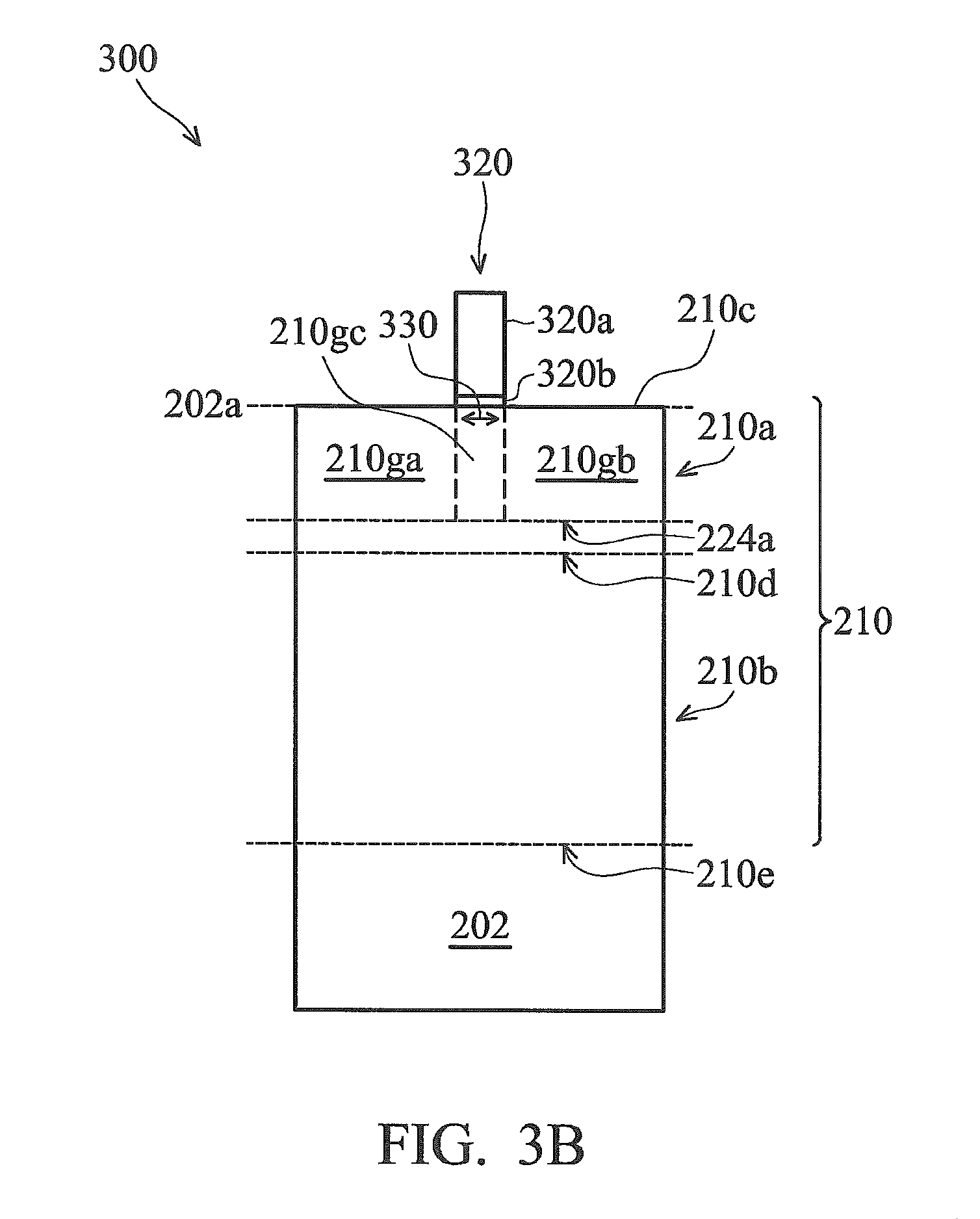
FIG. 3A-D shows a complete FINFET device 300 having a plurality of isolation structures 220 fabricated using the steps shown in FIG. 2A-H, wherein FIG. 3A shows a perspective view, and wherein FIGS. 3B-D show cross-section views taken along the respective lines of FIG. 3A. Similar features in FIGS. 2 and 3 are numbered the same for the sake of simplicity and clarity.
Referring to FIG. 3A, the FINFET 300 includes the plurality of fin structures 210 separated by the plurality of isolation structures 220. Each fin structure 210 extends in a longitudinal direction 210g. A gate structure 320 comprising a gate electrode 320a and a gate insulator 320b is disposed over the fin structures 210. FIG. 3A also illustrates the source/drain regions 330a, 330b, 329a and 329b of the FINFET 300.
FIG. 3B illustrates a cross-sectional view of the FINFET 300 taken along the line b-b of FIG. 3A. Each fin structure 210 extending in a longitudinal direction 210g comprises an upper portion 210a and a lower portion 210b separated at a transition location 210d at where the sidewall of the fin structure 210 at an angle of 85 degrees to the major surface 202a of the substrate 202, the upper portion 210a has sidewalls that are substantially perpendicular to the major surface 202a of the substrate 202 and a top surface 210c, the upper portion 210a comprises a first longitudinal portion 210ga, a second longitudinal portion 210gb, and a third longitudinal portion 210gc disposed between the first and the second longitudinal portions 210ga, 219gb. A channel region 330 is defined within the third longitudinal portion 210gc of the upper portion 210a. A gate structure 320 comprising a gate electrode 320a and a gate insulator 320b may be disposed over the channel region 330. A silicide layer (not shown) may be disposed within the first and the second longitudinal portions 210ga, 219gb form source/drain regions in the FINFET 300. The lower portion 210b under the upper portion 210a has a base 210e and bottom-up tapered sidewalls.
Referring to the cross sectional view of FIG. 3C taken along the line c-c of FIG. 3A, the gate structure 320 comprises the gate electrode 320a and the gate insulator 320b. The gate electrode 320a is disposed over the gate insulator 320b. If the thickness of the gate insulator 320b is uniform on all the surfaces of the fin structures 210, a triple gate transistor is formed. The channel 330 of the triple gate transistor is disposed under the gate structure 320 and within the top surface 210c and sidewalls of the third longitudinal portion 210gc of the upper portion 210a of the fin structures 210. However, in some embodiments, an additional dielectric layer (not shown) may be formed over the top surface 210c of the third longitudinal portion 210gc of the upper portion 210a before or after forming the gate insulator 310, the channel 330 of the FINFET 300 is formed only along the sidewalls of the third longitudinal portion 210gc, forming a double gate transistor.
FIG. 3D illustrates a cross-sectional view of the FINFET 300 taken along the line d-d of FIG. 3A. The fin structures 210 disposed between the isolation structures 220 are extending in a longitudinal direction 210g and continuous pieces of the underlying substrate 202. In some embodiments, the fin structures 210 may be separated from the substrate 202 by an insulation layer (not shown). In some embodiments, the first and the second longitudinal portions 210ga, 210gb of the upper portion 210a of the fin structures 210 comprise dopant-rich regions (not shown), and a silicide layer (not shown) may be disposed within the first and the second longitudinal portions 210ga, 210gb forming source/drain regions 329a and 329b in the FINFET 300. In various embodiments, the thickness of the dopant-rich regions is about 0.5 nm to about 10 nm. Then, subsequent processes, including interconnect processing, must be performed after forming the FINFET 300 to complete the IC fabrication.
While the invention has been described by way of example and in terms of the preferred embodiments, it is to be understood that the invention is not limited to the disclosed embodiments. To the contrary, it is intended to cover various modifications and similar arrangements (as would be apparent to those skilled in the art). Therefore, the scope of the appended claims should be accorded the broadest interpretation so as to encompass all such modifications and similar arrangements. The invention can be used to form or fabricate a fin structure for a FINFET having no isolation recess.
* * * * *
References
D00000
D00001
D00002
D00003
D00004
D00005
D00006
D00007
D00008
D00009
D00010
D00011
D00012

D00013

D00014
D00015

D00016

XML
uspto.report is an independent third-party trademark research tool that is not affiliated, endorsed, or sponsored by the United States Patent and Trademark Office (USPTO) or any other governmental organization. The information provided by uspto.report is based on publicly available data at the time of writing and is intended for informational purposes only.
While we strive to provide accurate and up-to-date information, we do not guarantee the accuracy, completeness, reliability, or suitability of the information displayed on this site. The use of this site is at your own risk. Any reliance you place on such information is therefore strictly at your own risk.
All official trademark data, including owner information, should be verified by visiting the official USPTO website at www.uspto.gov. This site is not intended to replace professional legal advice and should not be used as a substitute for consulting with a legal professional who is knowledgeable about trademark law.